Renesas Sh7781 Users Manual SH7785 Hardware
SH7781 to the manual 87234bda-05ed-fb94-49d4-cae2fef8fa49
2015-02-06
: Renesas Renesas-Sh7781-Users-Manual-523549 renesas-sh7781-users-manual-523549 renesas pdf
Open the PDF directly: View PDF ![]() .
.
Page Count: 1692 [warning: Documents this large are best viewed by clicking the View PDF Link!]
- Cover
- Notes regarding these materials
- General Precautions in the Handling of MPU/MCU Products
- Preface
- Contents
- Section 1 Overview
- Section 2 Programming Model
- Section 3 Instruction Set
- Section 4 Pipelining
- Section 5 Exception Handling
- Section 6 Floating-Point Unit (FPU)
- Section 7 Memory Management Unit (MMU)
- 7.1 Overview of MMU
- 7.2 Register Descriptions
- 7.2.1 Page Table Entry High Register (PTEH)
- 7.2.2 Page Table Entry Low Register (PTEL)
- 7.2.3 Translation Table Base Register (TTB)
- 7.2.4 TLB Exception Address Register (TEA)
- 7.2.5 MMU Control Register (MMUCR)
- 7.2.6 Page Table Entry Assistance Register (PTEA)
- 7.2.7 Physical Address Space Control Register (PASCR)
- 7.2.8 Instruction Re-Fetch Inhibit Control Register (IRMCR)
- 7.3 TLB Functions (TLB Compatible Mode; MMUCR.ME = 0)
- 7.4 TLB Functions (TLB Extended Mode; MMUCR.ME = 1)
- 7.5 MMU Functions
- 7.6 MMU Exceptions
- 7.7 Memory-Mapped TLB Configuration
- 7.8 32-Bit Address Extended Mode
- 7.9 32-Bit Boot Function
- 7.10 Usage Notes
- Section 8 Caches
- Section 9 On-Chip Memory
- Section 10 Interrupt Controller (INTC)
- Section 11 Local Bus State Controller (LBSC)
- 11.1 Features
- 11.2 Input/Output Pins
- 11.3 Overview of Areas
- 11.4 Register Descriptions
- 11.5 Operation
- 11.5.1 Endian/Access Size and Data Alignment
- 11.5.2 Areas
- 11.5.3 SRAM interface
- 11.5.4 Burst ROM Interface
- 11.5.5 PCMCIA Interface
- 11.5.6 MPX Interface
- 11.5.7 Byte Control SRAM Interface
- 11.5.8 Wait Cycles between Access Cycles
- 11.5.9 Bus Arbitration
- 11.5.10 Master Mode
- 11.5.11 Slave Mode
- 11.5.12 Cooperation between Master and Slave
- 11.5.13 Power-Down Mode and Bus Arbitration
- 11.5.14 Mode Pin Settings and General Input Output Port Settings about Data Bus Width
- 11.5.15 Pins Multiplexed with Other Modules Functions
- 11.5.16 Register Settings for Divided-Up DACKn Output
- Section 12 DDR2-SDRAM Interface (DBSC2)
- 12.1 Features
- 12.2 Input/Output Pins
- 12.3 Data Alignment
- 12.4 Register Descriptions
- 12.4.1 DBSC2 Status Register (DBSTATE)
- 12.4.2 SDRAM Operation Enable Register (DBEN)
- 12.4.3 SDRAM Command Control Register (DBCMDCNT)
- 12.4.4 SDRAM Configuration Setting Register (DBCONF)
- 12.4.5 SDRAM Timing Register 0 (DBTR0)
- 12.4.6 SDRAM Timing Register 1 (DBTR1)
- 12.4.7 SDRAM Timing Register 2 (DBTR2)
- 12.4.8 SDRAM Refresh Control Register 0 (DBRFCNT0)
- 12.4.9 SDRAM Refresh Control Register 1 (DBRFCNT1)
- 12.4.10 SDRAM Refresh Control Register 2 (DBRFCNT2)
- 12.4.11 SDRAM Refresh Status Register (DBRFSTS)
- 12.4.12 DDRPAD Frequency Setting Register (DBFREQ)
- 12.4.13 DDRPAD DIC, ODT, OCD Setting Register (DBDICODTOCD)
- 12.4.14 SDRAM Mode Setting Register (DBMRCNT)
- 12.5 DBSC2 Operation
- 12.5.1 Supported SDRAM Commands
- 12.5.2 SDRAM Command Issue
- 12.5.3 Initialization Sequence
- 12.5.4 Self-Refresh Operation
- 12.5.5 Auto-Refresh Operation
- 12.5.6 Regarding Address Multiplexing
- 12.5.7 Regarding SDRAM Access and Timing Constraints
- 12.5.8 Important Information Regarding Use of 8-Bank DDR2-SDRAM Products
- 12.5.9 Important Information Regarding ODT Control Signal Output to SDRAM
- 12.5.10 DDR2-SDRAM Power Supply Backup Function
- 12.5.11 Method for Securing Time Required for Initialization, Self-Refresh Cancellation, etc.
- 12.5.12 Regarding the Supported Clock Ratio
- 12.5.13 Regarding MCKE Signal Operation
- Section 13 PCI Controller (PCIC)
- Section 14 Direct Memory Access Controller (DMAC)
- 14.1 Features
- 14.2 Input/Output Pins
- 14.3 Register Descriptions
- 14.3.1 DMA Source Address Registers 0 to 11 (SAR0 to SAR11)
- 14.3.2 DMA Source Address Registers B0 to B3, B6 to B9 (SARB0 to SARB3, SARB6 to SARB9)
- 14.3.3 DMA Destination Address Registers 0 to 11 (DAR0 to DAR11)
- 14.3.4 DMA Destination Address Registers B0 to B3, B6 to B9 (DARB0 to DARB3, DARB6 to DARB9)
- 14.3.5 DMA Transfer Count Registers 0 to 11 (TCR0 to TCR11)
- 14.3.6 DMA Transfer Count Registers B0 to B3, B6 to B9 (TCRB0 to TCRB3, TCRB6 to TCRB9)
- 14.3.7 DMA Channel Control Registers 0 to 11 (CHCR0 to CHCR11)
- 14.3.8 DMA Operation Register 0, 1 (DMAOR0 and DMAOR1)
- 14.3.9 DMA Extended Resource Selectors 0 to 5 (DMARS0 to DMARS5)
- 14.4 Operation
- 14.5 DMAC Interrupt Sources
- 14.6 Usage Notes
- Section 15 Clock Pulse Generator (CPG)
- Section 16 Watchdog Timer and Reset (WDT)
- Section 17 Power-Down Mode
- Section 18 Timer Unit (TMU)
- Section 19 Display Unit (DU)
- 19.1 Features
- 19.2 Input/Output Pins
- 19.3 Register Descriptions
- 19.3.1 Display Unit System Control Register
- 19.3.2 Display Mode Register (DSMR)
- 19.3.3 Display Status Register (DSSR)
- 19.3.4 Display Unit Status Register Clear Register (DSRCR)
- 19.3.5 Display Unit Interrupt Enable Register (DIER)
- 19.3.6 Color Palette Control Register (CPCR)
- 19.3.7 Display Plane Priority Register (DPPR)
- 19.3.8 Display Unit Extensional Function Enable Register (DEFR)
- 19.3.9 Horizontal Display Start Register (HDSR)
- 19.3.10 Horizontal Display End Register (HDER)
- 19.3.11 Vertical Display Start Register (VDSR)
- 19.3.12 Vertical Display End Register (VDER)
- 19.3.13 Horizontal Cycle Register (HCR)
- 19.3.14 Horizontal Sync Width Register (HSWR)
- 19.3.15 Vertical Cycle Register (VCR)
- 19.3.16 Vertical Sync Point Register (VSPR)
- 19.3.17 Equal Pulse Width Register (EQWR)
- 19.3.18 Separation Width Register (SPWR)
- 19.3.19 CLAMP Signal Start Register (CLAMPSR)
- 19.3.20 CLAMP Signal Width Register (CLAMPWR)
- 19.3.21 DE Signal Start Register (DESR)
- 19.3.22 DE Signal Width Register (DEWR)
- 19.3.23 Color Palette 1 Transparent Color Register (CP1TR)
- 19.3.24 Color Palette 2 Transparent Color Register (CP2TR)
- 19.3.25 Color Palette 3 Transparent Color Register (CP3TR)
- 19.3.26 Color Palette 4 Transparent Color Register (CP4TR)
- 19.3.27 Display Off Mode Output Register (DOOR)
- 19.3.28 Color Detection Register (CDER)
- 19.3.29 Background Plane Output Register (BPOR)
- 19.3.30 Raster Interrupt Offset Register (RINTOFSR)
- 19.3.31 Plane n Mode Register (PnMR) (n = 1 to 6)
- 19.3.32 Plane n Memory Width Register (PnMWR) (n = 1 to 6)
- 19.3.33 Plane n Blending Ratio Register (PnALPHAR) (n = 1 to 6)
- 19.3.34 Plane n Display Size X Register (PnDSXR) (n = 1 to 6)
- 19.3.35 Plane n Display Size Y Register (PnDSYR) (n = 1 to 6)
- 19.3.36 Plane n Display Position X Register (PnDPXR) (n = 1 to 6)
- 19.3.37 Plane n Display Position Y Register (PnDPYR) (n = 1 to 6)
- 19.3.38 Plane n Display Area Start Address 0 Register (PnDSA0R) (n = 1 to 6)
- 19.3.39 Plane n Display Area Start Address 1 Register (PnDSA1R) (n = 1 to 6)
- 19.3.40 Plane n Start Position X Register (PnSPXR) (n = 1 to 6)
- 19.3.41 Plane n Start Position Y Register (PnSPYR) (n = 1 to 6)
- 19.3.42 Plane n Wrap Around Start Position Register (PnWASPR) (n = 1 to 6)
- 19.3.43 Plane n Wrap Around Memory Width Register (PnWAMWR) (n = 1 to 6)
- 19.3.44 Plane n Blinking Time Register (PnBTR) (n = 1 to 6)
- 19.3.45 Plane n Transparent Color 1 Register (PnTC1R) (n = 1 to 6)
- 19.3.46 Plane n Transparent Color 2 Register (PnTC2R) (n = 1 to 6)
- 19.3.47 Plane n Memory Length Register (PnMLR) (n = 1 to 6)
- 19.3.48 Color Palette 1 Register 000 to 255 (CP1_000R to CP1_255R)
- 19.3.49 Color Palette 2 Register 000 to 255 (CP2_000R to CP2_255R)
- 19.3.50 Color Palette 3 Register 000 to 255 (CP3_000R to CP3_255R)
- 19.3.51 Color Palette 4 Register 000 to 255 (CP4_000R to CP4_255R)
- 19.3.52 External Synchronization Control Register (ESCR)
- 19.3.53 Output Signal Timing Adjustment Register (OTAR)
- 19.4 Operation
- 19.4.1 Configuration of Output Screen
- 19.4.2 Display On/Off
- 19.4.3 Plane Parameter
- 19.4.4 Memory Allocation
- 19.4.5 Input Display Data Format
- 19.4.6 Output Data Format
- 19.4.7 Endian Conversion
- 19.4.8 Color Palettes
- 19.4.9 Superpositioning of Planes
- 19.4.10 Display Contention
- 19.4.11 Blinking
- 19.4.12 Scroll Display
- 19.4.13 Wraparound Display
- 19.4.14 Upper-Left Overflow Display
- 19.4.15 Double Buffer Control
- 19.4.16 Sync Mode
- 19.5 Display Control
- 19.6 Power-Down Sequence
- Section 20 Graphics Data Translation Accelerator (GDTA)
- 20.1 Features
- 20.2 GDTA Address Space
- 20.3 Register Descriptions
- 20.3.1 GA Mask Register (GACMR)
- 20.3.2 GA Enable Register (GACER)
- 20.3.3 GA Interrupt Source Indicating Register (GACISR)
- 20.3.4 GA Interrupt Source Indication Clear Register (GACICR)
- 20.3.5 GA Interrupt Enable Register (GACIER)
- 20.3.6 GA CL Input Data Alignment Register (DRCL_CTL)
- 20.3.7 GA CL Output Data Alignment Register (DWCL_CTL)
- 20.3.8 GA MC Input Data Alignment Register (DRMC_CTL)
- 20.3.9 GA MC Output Data Alignment Register (DWMC_CTL)
- 20.3.10 GA Buffer RAM 0 Data Alignment Register (DCP_CTL)
- 20.3.11 GA Buffer RAM 1 Data Alignment Register (DID_CTL)
- 20.3.12 CL Command FIFO (CLCF)
- 20.3.13 CL Control Register (CLCR)
- 20.3.14 CL Status Register (CLSR)
- 20.3.15 CL Frame Width Setting Register (CLWR)
- 20.3.16 CL Frame Height Setting Register (CLHR)
- 20.3.17 CL Input Y Padding Size Setting Register (CLIYPR)
- 20.3.18 CL Input UV Padding Size Setting Register (CLIUVPR)
- 20.3.19 CL Output Padding Size Setting Register (CLOPR)
- 20.3.20 CL Palette Pointer Register (CLPLPR)
- 20.3.21 MC Command FIFO (MCCF)
- 20.3.22 MC Status Register (MCSR)
- 20.3.23 MC Frame Width Setting Register (MCWR)
- 20.3.24 MC Frame Height Setting Register (MCHR)
- 20.3.25 MC Y Padding Size Setting Register (MCYPR)
- 20.3.26 MC UV Padding Size Setting Register (MCUVPR)
- 20.3.27 MC Output Frame Y Pointer Register (MCOYPR)
- 20.3.28 MC Output Frame U Pointer Register (MCOUPR)
- 20.3.29 MC Output Frame V Pointer Register (MCOVPR)
- 20.3.30 MC Past Frame Y Pointer Register (MCPYPR)
- 20.3.31 MC Past Frame U Pointer Register (MCPUPR)
- 20.3.32 MC Past Frame V Pointer Register (MCPVPR)
- 20.3.33 MC Future Frame Y Pointer Register (MCFYPR)
- 20.3.34 MC Future Frame U Pointer Register (MCFUPR)
- 20.3.35 MC Future Frame V Pointer Register (MCFVPR)
- 20.4 GDTA Operation
- 20.5 Interrupt Processing
- 20.6 Data Alignment
- 20.7 Usage Notes
- Section 21 Serial Communication Interface with FIFO (SCIF)
- 21.1 Features
- 21.2 Input/Output Pins
- 21.3 Register Descriptions
- 21.3.1 Receive Shift Register (SCRSR)
- 21.3.2 Receive FIFO Data Register (SCFRDR)
- 21.3.3 Transmit Shift Register (SCTSR)
- 21.3.4 Transmit FIFO Data Register (SCFTDR)
- 21.3.5 Serial Mode Register (SCSMR)
- 21.3.6 Serial Control Register (SCSCR)
- 21.3.7 Serial Status Register n (SCFSR)
- 21.3.8 Bit Rate Register n (SCBRR)
- 21.3.9 FIFO Control Register n (SCFCR)
- 21.3.10 Transmit FIFO Data Count Register n (SCTFDR)
- 21.3.11 Receive FIFO Data Count Register n (SCRFDR)
- 21.3.12 Serial Port Register n (SCSPTR)
- 21.3.13 Line Status Register n (SCLSR)
- 21.3.14 Serial Error Register n (SCRER)
- 21.4 Operation
- 21.5 SCIF Interrupt Sources and the DMAC
- 21.6 Usage Notes
- Section 22 Serial I/O with FIFO (SIOF)
- 22.1 Features
- 22.2 Input/Output Pins
- 22.3 Register Descriptions
- 22.3.1 Mode Register (SIMDR)
- 22.3.2 Control Register (SICTR)
- 22.3.3 Transmit Data Register (SITDR)
- 22.3.4 Receive Data Register (SIRDR)
- 22.3.5 Transmit Control Data Register (SITCR)
- 22.3.6 Receive Control Data Register (SIRCR)
- 22.3.7 Status Register (SISTR)
- 22.3.8 Interrupt Enable Register (SIIER)
- 22.3.9 FIFO Control Register (SIFCTR)
- 22.3.10 Clock Select Register (SISCR)
- 22.3.11 Transmit Data Assign Register (SITDAR)
- 22.3.12 Receive Data Assign Register (SIRDAR)
- 22.3.13 Control Data Assign Register (SICDAR)
- 22.4 Operation
- Section 23 Serial Peripheral Interface (HSPI)
- 23.1 Features
- 23.2 Input/Output Pins
- 23.3 Register Descriptions
- 23.4 Operation
- 23.4.1 Operation Overview with FIFO Mode Disabled
- 23.4.2 Operation with FIFO Mode Enabled
- 23.4.3 Timing Diagrams
- 23.4.4 HSPI Software Reset
- 23.4.5 Clock Polarity and Transmit Control
- 23.4.6 Transmit and Receive Routines
- 23.4.7 Flags and Interrupt Timing
- 23.4.8 Low-Power Consumption and Clock Synchronization
- Section 24 Multimedia Card Interface (MMCIF)
- 24.1 Features
- 24.2 Input/Output Pins
- 24.3 Register Descriptions
- 24.3.1 Command Registers 0 to 5 (CMDR0 to CMDR5)
- 24.3.2 Command Start Register (CMDSTRT)
- 24.3.3 Operation Control Register (OPCR)
- 24.3.4 Card Status Register (CSTR)
- 24.3.5 Interrupt Control Registers 0 to 2 (INTCR0 to INTCR2)
- 24.3.6 Interrupt Status Registers 0 to 2 (INTSTR0 to INTSTR2)
- 24.3.7 Transfer Clock Control Register (CLKON)
- 24.3.8 Command Timeout Control Register (CTOCR)
- 24.3.9 Transfer Byte Number Count Register (TBCR)
- 24.3.10 Mode Register (MODER)
- 24.3.11 Command Type Register (CMDTYR)
- 24.3.12 Response Type Register (RSPTYR)
- 24.3.13 Transfer Block Number Counter (TBNCR)
- 24.3.14 Response Registers 0 to 16, D (RSPR0 to RSPR16, RSPRD)
- 24.3.15 Data Timeout Register (DTOUTR)
- 24.3.16 Data Register (DR)
- 24.3.17 FIFO Pointer Clear Register (FIFOCLR)
- 24.3.18 DMA Control Register (DMACR)
- 24.4 Operation
- 24.5 MMCIF Interrupt Sources
- 24.6 Operations when Using DMA
- 24.7 Register Accesses with Little Endian Specification
- Section 25 Audio Codec Interface (HAC)
- 25.1 Features
- 25.2 Input/Output Pins
- 25.3 Register Descriptions
- 25.3.1 Control and Status Register (HACCR)
- 25.3.2 Command/Status Address Register (HACCSAR)
- 25.3.3 Command/Status Data Register (HACCSDR)
- 25.3.4 PCM Left Channel Register (HACPCML)
- 25.3.5 PCM Right Channel Register (HACPCMR)
- 25.3.6 TX Interrupt Enable Register (HACTIER)
- 25.3.7 TX Status Register (HACTSR)
- 25.3.8 RX Interrupt Enable Register (HACRIER)
- 25.3.9 RX Status Register (HACRSR)
- 25.3.10 HAC Control Register (HACACR)
- 25.4 AC 97 Frame Slot Structure
- 25.5 Operation
- Section 26 Serial Sound Interface (SSI) Module
- Section 27 NAND Flash Memory Controller (FLCTL)
- 27.1 Features
- 27.2 Input/Output Pins
- 27.3 Register Descriptions
- 27.3.1 Common Control Register (FLCMNCR)
- 27.3.2 Command Control Register (FLCMDCR)
- 27.3.3 Command Code Register (FLCMCDR)
- 27.3.4 Address Register (FLADR)
- 27.3.5 Address Register 2 (FLADR2)
- 27.3.6 Data Counter Register (FLDTCNTR)
- 27.3.7 Data Register (FLDATAR)
- 27.3.8 Interrupt DMA Control Register (FLINTDMACR)
- 27.3.9 Ready Busy Timeout Setting Register (FLBSYTMR)
- 27.3.10 Ready Busy Timeout Counter (FLBSYCNT)
- 27.3.11 Data FIFO Register (FLDTFIFO)
- 27.3.12 Control Code FIFO Register (FLECFIFO)
- 27.3.13 Transfer Control Register (FLTRCR)
- 27.4 Operation
- 27.5 Example of Register Setting
- 27.6 Interrupt Processing
- 27.7 DMA Transfer Settings
- Section 28 General Purpose I/O Ports (GPIO)
- 28.1 Features
- 28.2 Register Descriptions
- 28.2.1 Port A Control Register (PACR)
- 28.2.2 Port B Control Register (PBCR)
- 28.2.3 Port C Control Register (PCCR)
- 28.2.4 Port D Control Register (PDCR)
- 28.2.5 Port E Control Register (PECR)
- 28.2.6 Port F Control Register (PFCR)
- 28.2.7 Port G Control Register (PGCR)
- 28.2.8 Port H Control Register (PHCR)
- 28.2.9 Port J Control Register (PJCR)
- 28.2.10 Port K Control Register (PKCR)
- 28.2.11 Port L Control Register (PLCR)
- 28.2.12 Port M Control Register (PMCR)
- 28.2.13 Port N Control Register (PNCR)
- 28.2.14 Port P Control Register (PPCR)
- 28.2.15 Port Q Control Register (PQCR)
- 28.2.16 Port R Control Register (PRCR)
- 28.2.17 Port A Data Register (PADR)
- 28.2.18 Port B Data Register (PBDR)
- 28.2.19 Port C Data Register (PCDR)
- 28.2.20 Port D Data Register (PDDR)
- 28.2.21 Port E Data Register (PEDR)
- 28.2.22 Port F Data Register (PFDR)
- 28.2.23 Port G Data Register (PGDR)
- 28.2.24 Port H Data Register (PHDR)
- 28.2.25 Port J Data Register (PJDR)
- 28.2.26 Port K Data Register (PKDR)
- 28.2.27 Port L Data Register (PLDR)
- 28.2.28 Port M Data Register (PMDR)
- 28.2.29 Port N Data Register (PNDR)
- 28.2.30 Port P Data Register (PPDR)
- 28.2.31 Port Q Data Register (PQDR)
- 28.2.32 Port R Data Register (PRDR)
- 28.2.33 Port E Pull-Up Control Register (PEPUPR)
- 28.2.34 Port H Pull-Up Control Register (PHPUPR)
- 28.2.35 Port J Pull-Up Control Register (PJPUPR)
- 28.2.36 Port K Pull-Up Control Register (PKPUPR)
- 28.2.37 Port L Pull-Up Control Register (PLPUPR)
- 28.2.38 Port M Pull-Up Control Register (PMPUPR)
- 28.2.39 Port N Pull-Up Control Register (PNPUPR)
- 28.2.40 Input-Pin Pull-Up Control Register 1 (PPUPR1)
- 28.2.41 Input-Pin Pull-Up Control Register 2 (PPUPR2)
- 28.2.42 Peripheral Module Select Register 1 (P1MSELR)
- 28.2.43 Peripheral Module Select Register 2 (P2MSELR)
- 28.3 Usage Example
- Section 29 User Break Controller (UBC)
- 29.1 Features
- 29.2 Register Descriptions
- 29.2.1 Match Condition Setting Registers 0 and 1 (CBR0 and CBR1)
- 29.2.2 Match Operation Setting Registers 0 and 1 (CRR0 and CRR1)
- 29.2.3 Match Address Setting Registers 0 and 1 (CAR0 and CAR1)
- 29.2.4 Match Address Mask Setting Registers 0 and 1 (CAMR0 and CAMR1)
- 29.2.5 Match Data Setting Register 1 (CDR1)
- 29.2.6 Match Data Mask Setting Register 1 (CDMR1)
- 29.2.7 Execution Count Break Register 1 (CETR1)
- 29.2.8 Channel Match Flag Register (CCMFR)
- 29.2.9 Break Control Register (CBCR)
- 29.3 Operation Description
- 29.4 User Break Debugging Support Function
- 29.5 User Break Examples
- 29.6 Usage Notes
- Section 30 User Debugging Interface (H-UDI)
- Section 31 Register List
- Section 32 Electrical Characteristics
- 32.1 Absolute Maximum Ratings
- 32.2 DC Characteristics
- 32.3 AC Characteristics
- 32.3.1 Clock and Control Signal Timing
- 32.3.2 Control Signal Timing
- 32.3.3 Bus Timing
- 32.3.4 DBSC2 Signal Timing
- 32.3.5 INTC Module Signal Timing
- 32.3.6 PCIC Module Signal Timing
- 32.3.7 DMAC Module Signal Timing
- 32.3.8 TMU Module Signal Timing
- 32.3.9 SCIF Module Signal Timing
- 32.3.10 H-UDI Module Signal Timing
- 32.3.11 GPIO Signal Timing
- 32.3.12 HSPI Module Signal Timing
- 32.3.13 SIOF Module Signal Timing
- 32.3.14 MMCIF Module Signal Timing
- 32.3.15 HAC Interface Module Signal Timing
- 32.3.16 SSI Interface Module Signal Timing
- 32.3.17 FLCTL Module Signal Timing
- 32.3.18 Display Unit Signal Timing
- 32.4 AC Characteristic Test Conditions
- Appendix
- Colophon

Revision Date: Jan. 10
,
2008
32 Hardware Manual
Renesas 32-Bit RISC Microcomputer
SuperH™ RISC Engine Family
SH7780 Series
Rev.1.00
REJ09B0261-0100
SH7785

Rev.1.00 Jan. 10, 2008 Page ii of xxx
REJ09B0261-0100
1. This document is provided for reference purposes only so that Renesas customers may select the appropriate
Renesas products for their use. Renesas neither makes warranties or representations with respect to the
accuracy or completeness of the information contained in this document nor grants any license to any
intellectual property rights or any other rights of Renesas or any third party with respect to the information in
this document.
2. Renesas shall have no liability for damages or infringement of any intellectual property or other rights arising
out of the use of any information in this document, including, but not limited to, product data, diagrams, charts,
programs, algorithms, and application circuit examples.
3. You should not use the products or the technology described in this document for the purpose of military
applications such as the development of weapons of mass destruction or for the purpose of any other military
use. When exporting the products or technology described herein, you should follow the applicable export
control laws and regulations, and procedures required by such laws and regulations.
4. All information included in this document such as product data, diagrams, charts, programs, algorithms, and
application circuit examples, is current as of the date this document is issued. Such information, however, is
subject to change without any prior notice. Before purchasing or using any Renesas products listed in this
document, please confirm the latest product information with a Renesas sales office. Also, please pay regular
and careful attention to additional and different information to be disclosed by Renesas such as that disclosed
through our website. (http://www.renesas.com )
5. Renesas has used reasonable care in compiling the information included in this document, but Renesas
assumes no liability whatsoever for any damages incurred as a result of errors or omissions in the information
included in this document.
6. When using or otherwise relying on the information in this document, you should evaluate the information in
light of the total system before deciding about the applicability of such information to the intended application.
Renesas makes no representations, warranties or guaranties regarding the suitability of its products for any
particular application and specifically disclaims any liability arising out of the application and use of the
information in this document or Renesas products.
7. With the exception of products specified by Renesas as suitable for automobile applications, Renesas
products are not designed, manufactured or tested for applications or otherwise in systems the failure or
malfunction of which may cause a direct threat to human life or create a risk of human injury or which require
especially high quality and reliability such as safety systems, or equipment or systems for transportation and
traffic, healthcare, combustion control, aerospace and aeronautics, nuclear power, or undersea communication
transmission. If you are considering the use of our products for such purposes, please contact a Renesas
sales office beforehand. Renesas shall have no liability for damages arising out of the uses set forth above.
8. Notwithstanding the preceding paragraph, you should not use Renesas products for the purposes listed below:
(1) artificial life support devices or systems
(2) surgical implantations
(3) healthcare intervention (e.g., excision, administration of medication, etc.)
(4) any other purposes that pose a direct threat to human life
Renesas shall have no liability for damages arising out of the uses set forth in the above and purchasers who
elect to use Renesas products in any of the foregoing applications shall indemnify and hold harmless Renesas
Technology Corp., its affiliated companies and their officers, directors, and employees against any and all
damages arising out of such applications.
9. You should use the products described herein within the range specified by Renesas, especially with respect
to the maximum rating, operating supply voltage range, movement power voltage range, heat radiation
characteristics, installation and other product characteristics. Renesas shall have no liability for malfunctions or
damages arising out of the use of Renesas products beyond such specified ranges.
10. Although Renesas endeavors to improve the quality and reliability of its products, IC products have specific
characteristics such as the occurrence of failure at a certain rate and malfunctions under certain use
conditions. Please be sure to implement safety measures to guard against the possibility of physical injury, and
injury or damage caused by fire in the event of the failure of a Renesas product, such as safety design for
hardware and software including but not limited to redundancy, fire control and malfunction prevention,
appropriate treatment for aging degradation or any other applicable measures. Among others, since the
evaluation of microcomputer software alone is very difficult, please evaluate the safety of the final products or
system manufactured by you.
11. In case Renesas products listed in this document are detached from the products to which the Renesas
products are attached or affixed, the risk of accident such as swallowing by infants and small children is very
high. You should implement safety measures so that Renesas products may not be easily detached from your
products. Renesas shall have no liability for damages arising out of such detachment.
12. This document may not be reproduced or duplicated, in any form, in whole or in part, without prior written
approval from Renesas.
13. Please contact a Renesas sales office if you have any questions regarding the information contained in this
document, Renesas semiconductor products, or if you have any other inquiries.
Notes regarding these materials

Rev.1.00 Jan. 10, 2008 Page iii of xxx
REJ09B0261-0100
General Precautions in the Handling of MPU/MCU Products
The following usage notes are applicable to all MPU/MCU products from Renesas. For detailed usage notes
on the products covered by this manual, refer to the relevant sections of the manual. If the descriptions under
General Precautions in the Handling of MPU/MCU Products and in the body of the manual differ from each
other, the description in the body of the manual takes precedence.
1. Handling of Unused Pins
Handle unused pins in accord with the directions given under Handling of Unused Pins in
the manual.
The input pins of CMOS products are generally in the high-impedance state. In operation
with an unused pin in the open-circuit state, extra electromagnetic noise is induced in
the vicinity of LSI, an associated shoot-through current flows internally, and malfunctions
may occur due to the false recognition of the pin state as an input signal. Unused pins
should be handled as described under Handling of Unused Pins in the manual.
2. Processing at Power-on
The state of the product is undefined at the moment when power is supplied.
The states of internal circuits in the LSI are indeterminate and the states of register settings
and pins are undefined at the moment when power is supplied.
In a finished product where the reset signal is applied to the external reset pin, the
states of pins are not guaranteed from the moment when power is supplied until the
reset process is completed.
In a similar way, the states of pins in a product that is reset by an on-chip power-on
reset function are not guaranteed from the moment when power is supplied until the
power reaches the level at which resetting has been specified.
3. Prohibition of Access to Reserved Addresses
Access to reserved addresses is prohibited.
The reserved addresses are provided for the possible future expansion of functions. Do not
access these addresses; the correct operation of LSI is not guaranteed if they are
accessed.
4. Clock Signals
After applying a reset, only release the reset line after the operating clock signal has
become stable. When switching the clock signal during program execution, wait until the
target clock signal has stabilized.
When the clock signal is generated with an external resonator (or from an external
oscillator) during a reset, ensure that the reset line is only released after full stabilization
of the clock signal. Moreover, when switching to a clock signal produced with an
external resonator (or by an external oscillator) while program execution is in progress,
wait until the target clock signal is stable.
5. Differences between Products
Before changing from one product to another, i.e. to one with a different type number,
confirm that the change will not lead to problems.
The characteristics of MPU/MCU in the same group but having different type numbers may
differ because of the differences in internal memory capacity and layout pattern. When
changing to products of different type numbers, implement a system-evaluation test for
each of the products.

Rev.1.00 Jan. 10, 2008 Page iv of xxx
REJ09B0261-0100

Rev.1.00 Jan. 10, 2008 Page v of xxx
REJ09B0261-0100
Preface
This LSI is a RISC (Reduced Instruction Set Computer) microcomputer which includes a Renesas
Technology-original RISC CPU (SH-4A) and various peripheral functions required to configure a
system.
Target Users: This manual was written for users who will be using this LSI in the design of
application systems. Users of this manual are expected to understand the
fundamentals of electrical circuits, logical circuits, and microcomputers.
Objective: This manual was written to explain the hardware functions and electrical
characteristics of this LSI to the above users.
Notes on reading this manual:
• In order to understand the overall functions of the chip
Read the manual according to the contents. This manual consists of parts on the CPU, system
control functions, peripheral functions and electrical characteristics.
• In order to understand individual instructions in detail
Read the separate manuals SH-4A Extended Functions Software Manual and SH-4A Software
Manual.
Rules: Bit order: The MSB is on the left and the LSB is on the right.
Number notation: Binary is B'xxxx, hexadecimal is H'xxxx, decimal is xxxx.
Signal notation: An overbar is added to active-low signals: xxxx

Rev.1.00 Jan. 10, 2008 Page vi of xxx
REJ09B0261-0100
Abbreviations
ALU Arithmetic Logic Unit
ASID Address Space Identifier
BGA Ball Grid Array
CMT Timer/Counter (Compare Match Timer)
CPG Clock Pulse Generator
CPU Central Processing Unit
DDR Double Data Rate
DDRIF DDR-SDRAM Interface
DMA Direct Memory Access
DMAC Direct Memory Access Controller
FIFO First-In First-Out
FPU Floating-point Unit
HAC Audio Codec
H-UDI User Debugging Interface
INTC Interrupt Controller
JTAG Joint Test Action Group
LBSC Local Bus State Controller
LRAM L Memory
LRU Least Recently Used
LSB Least Significant Bit
MMCIF Multimedia Card Interface
MMU Memory Management Unit

Rev.1.00 Jan. 10, 2008 Page vii of xxx
REJ09B0261-0100
MSB Most Significant Bit
PC Program Counter
PCI Peripheral Component Interconnect
PCIC PCI (local bus) Controller
PFC Pin Function Controller
RISC Reduced Instruction Set Computer
RTC Realtime Clock
SCIF Serial Communication Interface with FIFO
SIOF Serial Interface with FIFO
SSI Serial Sound Interface
TAP Test Access Port
TLB Translation Lookaside Buffer
TMU Timer Unit
UART Universal Asynchronous Receiver/Transmitter
UBC User Break Controller
WDT Watchdog Timer

Rev.1.00 Jan. 10, 2008 Page viii of xxx
REJ09B0261-0100
All trademarks and registered trademarks are the property of their respective owners.

Rev.1.00 Jan. 10, 2008 Page ix of xxx
REJ09B0261-0100
Contents
Section 1 Overview.................................................................................................................. 1
1.1 Features of the SH7785..........................................................................................................1
1.2 Block Diagram..................................................................................................................... 13
1.3 Pin Arrangement Table ........................................................................................................ 14
1.4 Pin Arrangement .................................................................................................................. 22
1.5 Physical Memory Address Map........................................................................................... 24
Section 2 Programming Model........................................................................................... 25
2.1 Data Formats........................................................................................................................ 25
2.2 Register Descriptions ...........................................................................................................26
2.2.1 Privileged Mode and Banks.................................................................................. 26
2.2.2 General Registers.................................................................................................. 30
2.2.3 Floating-Point Registers ....................................................................................... 31
2.2.4 Control Registers .................................................................................................. 33
2.2.5 System Registers................................................................................................... 35
2.3 Memory-Mapped Registers.................................................................................................. 39
2.4 Data Formats in Registers.................................................................................................... 40
2.5 Data Formats in Memory ..................................................................................................... 40
2.6 Processing States.................................................................................................................. 41
2.7 Usage Notes ......................................................................................................................... 43
2.7.1 Notes on Self-Modifying Code............................................................................. 43
Section 3 Instruction Set....................................................................................................... 45
3.1 Execution Environment ....................................................................................................... 45
3.2 Addressing Modes ............................................................................................................... 47
3.3 Instruction Set...................................................................................................................... 52
Section 4 Pipelining............................................................................................................... 65
4.1 Pipelines............................................................................................................................... 65
4.2 Parallel-Executability........................................................................................................... 76
4.3 Issue Rates and Execution Cycles........................................................................................ 79
Section 5 Exception Handling ............................................................................................ 89
5.1 Summary of Exception Handling......................................................................................... 89
5.2 Register Descriptions ...........................................................................................................89
5.2.1 TRAPA Exception Register (TRA) ...................................................................... 90

Rev.1.00 Jan. 10, 2008 Page x of xxx
REJ09B0261-0100
5.2.2 Exception Event Register (EXPEVT)................................................................... 91
5.2.3 Interrupt Event Register (INTEVT)...................................................................... 92
5.2.4 Non-Support Detection Exception Register (EXPMASK) ................................... 93
5.3 Exception Handling Functions............................................................................................. 95
5.3.1 Exception Handling Flow ..................................................................................... 95
5.3.2 Exception Handling Vector Addresses ................................................................. 95
5.4 Exception Types and Priorities ............................................................................................ 96
5.5 Exception Flow.................................................................................................................... 98
5.5.1 Exception Flow..................................................................................................... 98
5.5.2 Exception Source Acceptance ............................................................................ 100
5.5.3 Exception Requests and BL Bit.......................................................................... 101
5.5.4 Return from Exception Handling........................................................................ 101
5.6 Description of Exceptions.................................................................................................. 102
5.6.1 Resets.................................................................................................................. 102
5.6.2 General Exceptions............................................................................................. 104
5.6.3 Interrupts............................................................................................................. 120
5.6.4 Priority Order with Multiple Exceptions ............................................................ 121
5.7 Usage Notes....................................................................................................................... 123
Section 6 Floating-Point Unit (FPU) .............................................................................. 125
6.1 Features.............................................................................................................................. 125
6.2 Data Formats...................................................................................................................... 126
6.2.1 Floating-Point Format......................................................................................... 126
6.2.2 Non-Numbers (NaN) .......................................................................................... 129
6.2.3 Denormalized Numbers ...................................................................................... 130
6.3 Register Descriptions......................................................................................................... 131
6.3.1 Floating-Point Registers ..................................................................................... 131
6.3.2 Floating-Point Status/Control Register (FPSCR) ............................................... 133
6.3.3 Floating-Point Communication Register (FPUL)............................................... 136
6.4 Rounding............................................................................................................................ 137
6.5 Floating-Point Exceptions.................................................................................................. 138
6.5.1 General FPU Disable Exceptions and Slot FPU Disable Exceptions ................. 138
6.5.2 FPU Exception Sources ...................................................................................... 138
6.5.3 FPU Exception Handling.................................................................................... 139
6.6 Graphics Support Functions............................................................................................... 140
6.6.1 Geometric Operation Instructions....................................................................... 140
6.6.2 Pair Single-Precision Data Transfer.................................................................... 141
Section 7 Memory Management Unit (MMU) ............................................................ 143
7.1 Overview of MMU ............................................................................................................ 144

Rev.1.00 Jan. 10, 2008 Page xi of xxx
REJ09B0261-0100
7.1.1 Address Spaces ................................................................................................... 146
7.2 Register Descriptions ......................................................................................................... 152
7.2.1 Page Table Entry High Register (PTEH)............................................................ 153
7.2.2 Page Table Entry Low Register (PTEL) ............................................................. 154
7.2.3 Translation Table Base Register (TTB).............................................................. 155
7.2.4 TLB Exception Address Register (TEA) ............................................................ 156
7.2.5 MMU Control Register (MMUCR) .................................................................... 156
7.2.6 Page Table Entry Assistance Register (PTEA)................................................... 159
7.2.7 Physical Address Space Control Register (PASCR)........................................... 160
7.2.8 Instruction Re-Fetch Inhibit Control Register (IRMCR) .................................... 162
7.3 TLB Functions (TLB Compatible Mode; MMUCR.ME = 0)............................................ 164
7.3.1 Unified TLB (UTLB) Configuration .................................................................. 164
7.3.2 Instruction TLB (ITLB) Configuration............................................................... 167
7.3.3 Address Translation Method............................................................................... 167
7.4 TLB Functions (TLB Extended Mode; MMUCR.ME = 1) ............................................... 170
7.4.1 Unified TLB (UTLB) Configuration .................................................................. 170
7.4.2 Instruction TLB (ITLB) Configuration............................................................... 173
7.4.3 Address Translation Method............................................................................... 174
7.5 MMU Functions................................................................................................................. 177
7.5.1 MMU Hardware Management............................................................................ 177
7.5.2 MMU Software Management ............................................................................. 177
7.5.3 MMU Instruction (LDTLB)................................................................................ 178
7.5.4 Hardware ITLB Miss Handling .......................................................................... 180
7.5.5 Avoiding Synonym Problems............................................................................. 181
7.6 MMU Exceptions............................................................................................................... 182
7.6.1 Instruction TLB Multiple Hit Exception............................................................. 182
7.6.2 Instruction TLB Miss Exception......................................................................... 183
7.6.3 Instruction TLB Protection Violation Exception ................................................ 184
7.6.4 Data TLB Multiple Hit Exception ...................................................................... 185
7.6.5 Data TLB Miss Exception .................................................................................. 185
7.6.6 Data TLB Protection Violation Exception.......................................................... 187
7.6.7 Initial Page Write Exception............................................................................... 188
7.7 Memory-Mapped TLB Configuration................................................................................ 190
7.7.1 ITLB Address Array ........................................................................................... 191
7.7.2 ITLB Data Array (TLB Compatible Mode)........................................................ 192
7.7.3 ITLB Data Array (TLB Extended Mode) ........................................................... 193
7.7.4 UTLB Address Array.......................................................................................... 195
7.7.5 UTLB Data Array (TLB Compatible Mode) ...................................................... 196
7.7.6 UTLB Data Array (TLB Extended Mode).......................................................... 197
7.8 32-Bit Address Extended Mode......................................................................................... 199

Rev.1.00 Jan. 10, 2008 Page xii of xxx
REJ09B0261-0100
7.8.1 Overview of 32-Bit Address Extended Mode..................................................... 199
7.8.2 Transition to 32-Bit Address Extended Mode .................................................... 200
7.8.3 Privileged Space Mapping Buffer (PMB) Configuration ................................... 200
7.8.4 PMB Function..................................................................................................... 202
7.8.5 Memory-Mapped PMB Configuration ............................................................... 203
7.8.6 Notes on Using 32-Bit Address Extended Mode................................................ 204
7.9 32-Bit Boot Function ......................................................................................................... 207
7.9.1 Initial Entries to PMB......................................................................................... 207
7.9.2 Notes on 32-Bit Boot.......................................................................................... 207
7.10 Usage Notes....................................................................................................................... 209
7.10.1 Note on Using LDTLB Instruction..................................................................... 209
Section 8 Caches................................................................................................................... 211
8.1 Features.............................................................................................................................. 211
8.2 Register Descriptions......................................................................................................... 215
8.2.1 Cache Control Register (CCR) ........................................................................... 216
8.2.2 Queue Address Control Register 0 (QACR0)..................................................... 218
8.2.3 Queue Address Control Register 1 (QACR1)..................................................... 219
8.2.4 On-Chip Memory Control Register (RAMCR) .................................................. 220
8.3 Operand Cache Operation.................................................................................................. 222
8.3.1 Read Operation ................................................................................................... 222
8.3.2 Prefetch Operation.............................................................................................. 223
8.3.3 Write Operation .................................................................................................. 224
8.3.4 Write-Back Buffer .............................................................................................. 225
8.3.5 Write-Through Buffer......................................................................................... 225
8.3.6 OC Two-Way Mode ........................................................................................... 226
8.4 Instruction Cache Operation .............................................................................................. 227
8.4.1 Read Operation ................................................................................................... 227
8.4.2 Prefetch Operation.............................................................................................. 227
8.4.3 IC Two-Way Mode............................................................................................. 228
8.4.4 Instruction Cache Way Prediction Operation ..................................................... 228
8.5 Cache Operation Instruction .............................................................................................. 229
8.5.1 Coherency between Cache and External Memory.............................................. 229
8.5.2 Prefetch Operation.............................................................................................. 231
8.6 Memory-Mapped Cache Configuration ............................................................................. 232
8.6.1 IC Address Array................................................................................................ 232
8.6.2 IC Data Array ..................................................................................................... 234
8.6.3 OC Address Array .............................................................................................. 234
8.6.4 OC Data Array.................................................................................................... 236
8.6.5 Memory-Mapped Cache Associative Write Operation....................................... 237

Rev.1.00 Jan. 10, 2008 Page xiii of xxx
REJ09B0261-0100
8.7 Store Queues ...................................................................................................................... 238
8.7.1 SQ Configuration................................................................................................ 238
8.7.2 Writing to SQ...................................................................................................... 238
8.7.3 Transfer to External Memory.............................................................................. 239
8.7.4 Determination of SQ Access Exception.............................................................. 240
8.7.5 Reading from SQ ................................................................................................ 240
8.8 Notes on Using 32-Bit Address Extended Mode ............................................................... 241
Section 9 On-Chip Memory .............................................................................................. 243
9.1 Features.............................................................................................................................. 243
9.2 Register Descriptions ......................................................................................................... 246
9.2.1 On-Chip Memory Control Register (RAMCR) .................................................. 247
9.2.2 OL memory Transfer Source Address Register 0 (LSA0).................................. 248
9.2.3 OL memory Transfer Source Address Register 1 (LSA1).................................. 250
9.2.4 OL memory Transfer Destination Address Register 0 (LDA0).......................... 252
9.2.5 OL memory Transfer Destination Address Register 1 (LDA1).......................... 254
9.3 Operation ........................................................................................................................... 256
9.3.1 Instruction Fetch Access from the CPU.............................................................. 256
9.3.2 Operand Access from the CPU and Access from the FPU ................................. 256
9.3.3 Access from the SuperHyway Bus Master Module ............................................ 257
9.3.4 OL Memory Block Transfer ............................................................................... 257
9.4 On-Chip Memory Protective Functions ............................................................................. 260
9.5 Usage Notes ....................................................................................................................... 261
9.5.1 Page Conflict ...................................................................................................... 261
9.5.2 Access Across Different Pages ........................................................................... 261
9.5.3 On-Chip Memory Coherency ............................................................................. 261
9.5.4 Sleep Mode ......................................................................................................... 262
9.6 Note on Using 32-Bit Address Extended Mode................................................................. 262
Section 10 Interrupt Controller (INTC) ......................................................................... 263
10.1 Features.............................................................................................................................. 263
10.1.1 Interrupt Method................................................................................................. 266
10.1.2 Interrupt Sources................................................................................................. 267
10.2 Input/Output Pins...............................................................................................................272
10.3 Register Descriptions ......................................................................................................... 273
10.3.1 External Interrupt Request Registers .................................................................. 277
10.3.2 User Mode Interrupt Disable Function ............................................................... 298
10.3.3 On-chip Module Interrupt Priority Registers ...................................................... 300
10.3.4 Individual On-Chip Module Interrupt Source Registers (INT2B0 to INT2B7).. 314
10.3.5 GPIO Interrupt Set Register (INT2GPIC) .......................................................... 322

Rev.1.00 Jan. 10, 2008 Page xiv of xxx
REJ09B0261-0100
10.4 Interrupt Sources................................................................................................................ 324
10.4.1 NMI Interrupts.................................................................................................... 324
10.4.2 IRQ Interrupts..................................................................................................... 324
10.4.3 IRL Interrupts ..................................................................................................... 325
10.4.4 On-Chip Peripheral Module Interrupts ............................................................... 327
10.4.5 Priority of On-Chip Peripheral Module Interrupts.............................................. 328
10.4.6 Interrupt Exception Handling and Priority ......................................................... 329
10.5 Operation ........................................................................................................................... 337
10.5.1 Interrupt Sequence.............................................................................................. 337
10.5.2 Multiple Interrupts.............................................................................................. 339
10.5.3 Interrupt Masking by MAI Bit............................................................................ 339
10.6 Interrupt Response Time.................................................................................................... 340
10.7 Usage Notes....................................................................................................................... 343
10.7.1 Example of Handing Routine of IRL Interrupts and Level Detection
IRQ Interrupts when ICR0.LVLMODE = 0 ....................................................... 343
10.7.2 Notes on Setting IRQ/IRL[7:0] Pin Function ..................................................... 344
10.7.3 Clearing IRQ and IRL Interrupt Requests .......................................................... 345
Section 11 Local Bus State Controller (LBSC)........................................................... 347
11.1 Features.............................................................................................................................. 347
11.2 Input/Output Pins...............................................................................................................350
11.3 Overview of Areas ............................................................................................................. 354
11.3.1 Space Divisions .................................................................................................. 354
11.3.2 Memory Bus Width ............................................................................................ 357
11.3.3 PCMCIA Support ............................................................................................... 358
11.4 Register Descriptions......................................................................................................... 362
11.4.1 Memory Address Map Select Register (MMSELR)........................................... 364
11.4.2 Bus Control Register (BCR) ............................................................................... 367
11.4.3 CSn Bus Control Register (CSnBCR) ................................................................ 371
11.4.4 CSn Wait Control Register (CSnWCR).............................................................. 377
11.4.5 CSn PCMCIA Control Register (CSnPCR)........................................................ 382
11.5 Operation ........................................................................................................................... 387
11.5.1 Endian/Access Size and Data Alignment ........................................................... 387
11.5.2 Areas................................................................................................................... 398
11.5.3 SRAM interface.................................................................................................. 403
11.5.4 Burst ROM Interface .......................................................................................... 412
11.5.5 PCMCIA Interface.............................................................................................. 416
11.5.6 MPX Interface .................................................................................................... 427
11.5.7 Byte Control SRAM Interface ............................................................................ 441
11.5.8 Wait Cycles between Access Cycles .................................................................. 446

Rev.1.00 Jan. 10, 2008 Page xv of xxx
REJ09B0261-0100
11.5.9 Bus Arbitration ................................................................................................... 448
11.5.10 Master Mode....................................................................................................... 450
11.5.11 Slave Mode ......................................................................................................... 451
11.5.12 Cooperation between Master and Slave.............................................................. 451
11.5.13 Power-Down Mode and Bus Arbitration ............................................................ 451
11.5.14 Mode Pin Settings and General Input Output Port Settings about
Data Bus Width................................................................................................... 452
11.5.15 Pins Multiplexed with Other Modules Functions ............................................... 452
11.5.16 Register Settings for Divided-Up DACKn Output ............................................. 452
Section 12 DDR2-SDRAM Interface (DBSC2).......................................................... 457
12.1 Features.............................................................................................................................. 457
12.2 Input/Output Pins...............................................................................................................460
12.3 Data Alignment..................................................................................................................465
12.4 Register Descriptions ......................................................................................................... 479
12.4.1 DBSC2 Status Register (DBSTATE) ................................................................. 482
12.4.2 SDRAM Operation Enable Register (DBEN)..................................................... 483
12.4.3 SDRAM Command Control Register (DBCMDCNT) ....................................... 484
12.4.4 SDRAM Configuration Setting Register (DBCONF)......................................... 486
12.4.5 SDRAM Timing Register 0 (DBTR0)................................................................ 488
12.4.6 SDRAM Timing Register 1 (DBTR1)................................................................ 492
12.4.7 SDRAM Timing Register 2 (DBTR2)................................................................ 495
12.4.8 SDRAM Refresh Control Register 0 (DBRFCNT0) .......................................... 499
12.4.9 SDRAM Refresh Control Register 1 (DBRFCNT1) .......................................... 500
12.4.10 SDRAM Refresh Control Register 2 (DBRFCNT2) .......................................... 502
12.4.11 SDRAM Refresh Status Register (DBRFSTS)................................................... 504
12.4.12 DDRPAD Frequency Setting Register (DBFREQ) ............................................ 505
12.4.13 DDRPAD DIC, ODT, OCD Setting Register (DBDICODTOCD)..................... 507
12.4.14 SDRAM Mode Setting Register (DBMRCNT) .................................................. 510
12.5 DBSC2 Operation .............................................................................................................. 512
12.5.1 Supported SDRAM Commands.......................................................................... 512
12.5.2 SDRAM Command Issue ................................................................................... 513
12.5.3 Initialization Sequence........................................................................................ 516
12.5.4 Self-Refresh Operation ....................................................................................... 517
12.5.5 Auto-Refresh Operation...................................................................................... 520
12.5.6 Regarding Address Multiplexing........................................................................ 521
12.5.7 Regarding SDRAM Access and Timing Constraints.......................................... 530
12.5.8 Important Information Regarding Use of 8-Bank DDR2-SDRAM Products ..... 544
12.5.9 Important Information Regarding ODT Control Signal Output to SDRAM ...... 544
12.5.10 DDR2-SDRAM Power Supply Backup Function............................................... 546

Rev.1.00 Jan. 10, 2008 Page xvi of xxx
REJ09B0261-0100
12.5.11 Method for Securing Time Required for Initialization, Self-Refresh
Cancellation, etc. ................................................................................................ 549
12.5.12 Regarding the Supported Clock Ratio ................................................................ 549
12.5.13 Regarding MCKE Signal Operation ................................................................... 550
Section 13 PCI Controller (PCIC)................................................................................... 551
13.1 Features.............................................................................................................................. 551
13.2 Input/Output Pins...............................................................................................................554
13.3 Register Descriptions......................................................................................................... 557
13.3.1 PCIC Enable Control Register (PCIECR) .......................................................... 562
13.3.2 Configuration Registers ...................................................................................... 563
13.3.3 PCI Local Registers ............................................................................................ 590
13.4 Operation ........................................................................................................................... 630
13.4.1 Supported PCI Commands ................................................................................. 630
13.4.2 PCIC Initialization.............................................................................................. 631
13.4.3 Master Access..................................................................................................... 632
13.4.4 Target Access ..................................................................................................... 640
13.4.5 Host Mode .......................................................................................................... 648
13.4.6 Normal Mode...................................................................................................... 651
13.4.7 Power Management ............................................................................................ 651
13.4.8 PCI Local Bus Basic Interface............................................................................ 653
Section 14 Direct Memory Access Controller (DMAC)........................................... 665
14.1 Features.............................................................................................................................. 665
14.2 Input/Output Pins...............................................................................................................667
14.3 Register Descriptions......................................................................................................... 668
14.3.1 DMA Source Address Registers 0 to 11 (SAR0 to SAR11)............................... 675
14.3.2 DMA Source Address Registers B0 to B3, B6 to B9
(SARB0 to SARB3, SARB6 to SARB9)............................................................ 676
14.3.3 DMA Destination Address Registers 0 to 11 (DAR0 to DAR11) ...................... 677
14.3.4 DMA Destination Address Registers B0 to B3, B6 to B9
(DARB0 to DARB3, DARB6 to DARB9) ......................................................... 678
14.3.5 DMA Transfer Count Registers 0 to 11 (TCR0 to TCR11)................................ 679
14.3.6 DMA Transfer Count Registers B0 to B3, B6 to B9
(TCRB0 to TCRB3, TCRB6 to TCRB9)............................................................ 680
14.3.7 DMA Channel Control Registers 0 to 11 (CHCR0 to CHCR11) ....................... 681
14.3.8 DMA Operation Register 0, 1 (DMAOR0 and DMAOR1)................................ 689
14.3.9 DMA Extended Resource Selectors 0 to 5 (DMARS0 to DMARS5)................. 693
14.4 Operation ........................................................................................................................... 701
14.4.1 DMA Transfer Requests ..................................................................................... 701

Rev.1.00 Jan. 10, 2008 Page xvii of xxx
REJ09B0261-0100
14.4.2 Channel Priority.................................................................................................. 706
14.4.3 DMA Transfer Types.......................................................................................... 709
14.4.4 DMA Transfer Flow ........................................................................................... 717
14.4.5 Repeat Mode Transfer ........................................................................................ 719
14.4.6 Reload Mode Transfer ........................................................................................ 720
14.4.7 DREQ Pin Sampling Timing .............................................................................. 721
14.5 DMAC Interrupt Sources................................................................................................... 729
14.6 Usage Notes ....................................................................................................................... 730
14.6.1 Stopping Modules and Changing Frequency ...................................................... 730
14.6.2 Address Error...................................................................................................... 730
14.6.3 NMI Interrupt...................................................................................................... 730
14.6.4 Burst Mode Transfer........................................................................................... 730
14.6.5 Divided-Up DACK Output................................................................................. 730
14.6.6 DACK/DREQ Setting......................................................................................... 731
Section 15 Clock Pulse Generator (CPG) ..................................................................... 733
15.1 Features.............................................................................................................................. 733
15.2 Input/Output Pins...............................................................................................................736
15.3 Clock Operating Modes ..................................................................................................... 737
15.4 Register Descriptions ......................................................................................................... 739
15.4.1 Frequency Control Register 0 (FRQCR0) .......................................................... 741
15.4.2 Frequency Control Register 1 (FRQCR1) .......................................................... 742
15.4.3 Frequency Display Register 1 (FRQMR1) ......................................................... 745
15.4.4 PLL Control Register (PLLCR).......................................................................... 747
15.5 Calculating the Frequency ................................................................................................. 748
15.6 How to Change the Frequency........................................................................................... 749
15.6.1 Changing the Frequency of Clocks Other than the Bus Clock ........................... 749
15.6.2 Changing the Bus Clock Frequency ................................................................... 749
15.7 Notes on Designing Board ................................................................................................. 756
Section 16 Watchdog Timer and Reset (WDT)........................................................... 759
16.1 Features.............................................................................................................................. 759
16.2 Input/Output Pins...............................................................................................................761
16.3 Register Descriptions ......................................................................................................... 762
16.3.1 Watchdog Timer Stop Time Register (WDTST)................................................ 763
16.3.2 Watchdog Timer Control/Status Register (WDTCSR)....................................... 764
16.3.3 Watchdog Timer Base Stop Time Register (WDTBST)..................................... 766
16.3.4 Watchdog Timer Counter (WDTCNT)............................................................... 767
16.3.5 Watchdog Timer Base Counter (WDTBCNT) ................................................... 768
16.4 Operation ........................................................................................................................... 769

Rev.1.00 Jan. 10, 2008 Page xviii of xxx
REJ09B0261-0100
16.4.1 Reset Request ..................................................................................................... 769
16.4.2 Using Watchdog Timer Mode ............................................................................ 771
16.4.3 Using Interval Timer Mode ................................................................................ 771
16.4.4 Time until WDT Counters Overflow.................................................................. 772
16.4.5 Clearing WDT Counters ..................................................................................... 773
16.5 Status Pin Change Timing during Reset ............................................................................ 774
16.5.1 Power-On Reset by PRESET Pin ....................................................................... 774
16.5.2 Power-On Reset by Watchdog Timer Overflow................................................. 777
16.5.3 Manual Reset by Watchdog Timer Overflow..................................................... 779
Section 17 Power-Down Mode ........................................................................................ 781
17.1 Features.............................................................................................................................. 781
17.1.1 Types of Power-Down Modes ............................................................................ 781
17.2 Input/Output Pins...............................................................................................................783
17.3 Register Descriptions......................................................................................................... 783
17.3.1 Sleep Control Register (SLPCR) ........................................................................ 785
17.3.2 Standby Control Register 0 (MSTPCR0) ........................................................... 786
17.3.3 Standby Control Register 1 (MSTPCR1) ........................................................... 789
17.3.4 Standby Display Register (MSTPMR) ............................................................... 791
17.4 Sleep Mode ........................................................................................................................ 793
17.4.1 Transition to Sleep Mode.................................................................................... 793
17.4.2 Releasing Sleep Mode ........................................................................................ 793
17.5 Deep Sleep Mode............................................................................................................... 794
17.5.1 Transition to Deep Sleep Mode .......................................................................... 794
17.5.2 Releasing Deep Sleep Mode............................................................................... 795
17.6 Module Standby Functions ................................................................................................ 796
17.6.1 Transition to Module Standby Mode .................................................................. 796
17.6.2 Releasing Module Standby Functions ................................................................ 796
17.7 Timing of the Changes on the STATUS Pins .................................................................... 797
17.7.1 Reset ................................................................................................................... 797
17.7.2 Releasing Sleep Mode ........................................................................................ 797
17.8 DDR-SDRAM Power Supply Backup............................................................................... 797
Section 18 Timer Unit (TMU).......................................................................................... 799
18.1 Features.............................................................................................................................. 799
18.2 Input/Output Pins...............................................................................................................801
18.3 Register Descriptions......................................................................................................... 802
18.3.1 Timer Start Registers (TSTRn) (n = 0, 1)........................................................... 804
18.3.2 Timer Constant Registers (TCORn) (n = 0 to 5) ................................................ 806
18.3.3 Timer Counters (TCNTn) (n = 0 to 5) ................................................................ 806

Rev.1.00 Jan. 10, 2008 Page xix of xxx
REJ09B0261-0100
18.3.4 Timer Control Registers (TCRn) (n = 0 to 5) ..................................................... 807
18.3.5 Input Capture Register 2 (TCPR2) ..................................................................... 809
18.4 Operation ........................................................................................................................... 810
18.4.1 Counter Operation .............................................................................................. 810
18.4.2 Input Capture Function ....................................................................................... 813
18.5 Interrupts............................................................................................................................ 814
18.6 Usage Notes ....................................................................................................................... 815
18.6.1 Register Writes ................................................................................................... 815
18.6.2 Reading from TCNT........................................................................................... 815
18.6.3 External Clock Frequency .................................................................................. 815
Section 19 Display Unit (DU) .......................................................................................... 817
19.1 Features.............................................................................................................................. 817
19.2 Input/Output Pins...............................................................................................................820
19.3 Register Descriptions ......................................................................................................... 821
19.3.1 Display Unit System Control Register................................................................ 841
19.3.2 Display Mode Register (DSMR) ........................................................................ 845
19.3.3 Display Status Register (DSSR) ......................................................................... 849
19.3.4 Display Unit Status Register Clear Register (DSRCR) ...................................... 853
19.3.5 Display Unit Interrupt Enable Register (DIER).................................................. 854
19.3.6 Color Palette Control Register (CPCR) .............................................................. 857
19.3.7 Display Plane Priority Register (DPPR) ............................................................. 859
19.3.8 Display Unit Extensional Function Enable Register (DEFR)............................. 862
19.3.9 Horizontal Display Start Register (HDSR)......................................................... 864
19.3.10 Horizontal Display End Register (HDER).......................................................... 865
19.3.11 Vertical Display Start Register (VDSR) ............................................................. 866
19.3.12 Vertical Display End Register (VDER).............................................................. 867
19.3.13 Horizontal Cycle Register (HCR)....................................................................... 868
19.3.14 Horizontal Sync Width Register (HSWR) .......................................................... 869
19.3.15 Vertical Cycle Register (VCR) ........................................................................... 870
19.3.16 Vertical Sync Point Register (VSPR) ................................................................. 871
19.3.17 Equal Pulse Width Register (EQWR)................................................................. 872
19.3.18 Separation Width Register (SPWR).................................................................... 873
19.3.19 CLAMP Signal Start Register (CLAMPSR) ...................................................... 874
19.3.20 CLAMP Signal Width Register (CLAMPWR)................................................... 875
19.3.21 DE Signal Start Register (DESR) ....................................................................... 876
19.3.22 DE Signal Width Register (DEWR) ................................................................... 877
19.3.23 Color Palette 1 Transparent Color Register (CP1TR)......................................... 878
19.3.24 Color Palette 2 Transparent Color Register (CP2TR)......................................... 881
19.3.25 Color Palette 3 Transparent Color Register (CP3TR)......................................... 884

Rev.1.00 Jan. 10, 2008 Page xx of xxx
REJ09B0261-0100
19.3.26 Color Palette 4 Transparent Color Register (CP4TR) ........................................ 887
19.3.27 Display Off Mode Output Register (DOOR)...................................................... 890
19.3.28 Color Detection Register (CDER) ...................................................................... 891
19.3.29 Background Plane Output Register (BPOR)....................................................... 892
19.3.30 Raster Interrupt Offset Register (RINTOFSR) ................................................... 894
19.3.31 Plane n Mode Register (PnMR) (n = 1 to 6)....................................................... 895
19.3.32 Plane n Memory Width Register (PnMWR) (n = 1 to 6).................................... 898
19.3.33 Plane n Blending Ratio Register (PnALPHAR) (n = 1 to 6) .............................. 899
19.3.34 Plane n Display Size X Register (PnDSXR) (n = 1 to 6).................................... 901
19.3.35 Plane n Display Size Y Register (PnDSYR) (n = 1 to 6).................................... 902
19.3.36 Plane n Display Position X Register (PnDPXR) (n = 1 to 6).............................. 903
19.3.37 Plane n Display Position Y Register (PnDPYR) (n = 1 to 6).............................. 904
19.3.38 Plane n Display Area Start Address 0 Register (PnDSA0R) (n = 1 to 6) ........... 905
19.3.39 Plane n Display Area Start Address 1 Register (PnDSA1R) (n = 1 to 6) ........... 906
19.3.40 Plane n Start Position X Register (PnSPXR) (n = 1 to 6) ................................... 907
19.3.41 Plane n Start Position Y Register (PnSPYR) (n = 1 to 6) ................................... 908
19.3.42 Plane n Wrap Around Start Position Register (PnWASPR) (n = 1 to 6) ............ 909
19.3.43 Plane n Wrap Around Memory Width Register (PnWAMWR) (n = 1 to 6) ...... 910
19.3.44 Plane n Blinking Time Register (PnBTR) (n = 1 to 6) ....................................... 911
19.3.45 Plane n Transparent Color 1 Register (PnTC1R) (n = 1 to 6)............................. 912
19.3.46 Plane n Transparent Color 2 Register (PnTC2R) (n = 1 to 6)............................. 913
19.3.47 Plane n Memory Length Register (PnMLR) (n = 1 to 6).................................... 914
19.3.48 Color Palette 1 Register 000 to 255 (CP1_000R to CP1_255R) ........................ 915
19.3.49 Color Palette 2 Register 000 to 255 (CP2_000R to CP2_255R) ........................ 916
19.3.50 Color Palette 3 Register 000 to 255 (CP3_000R to CP3_255R) ........................ 918
19.3.51 Color Palette 4 Register 000 to 255 (CP4_000R to CP4_255R) ........................ 919
19.3.52 External Synchronization Control Register (ESCR)........................................... 921
19.3.53 Output Signal Timing Adjustment Register (OTAR) ......................................... 923
19.4 Operation ........................................................................................................................... 930
19.4.1 Configuration of Output Screen.......................................................................... 930
19.4.2 Display On/Off ................................................................................................... 933
19.4.3 Plane Parameter .................................................................................................. 934
19.4.4 Memory Allocation............................................................................................. 936
19.4.5 Input Display Data Format ................................................................................. 937
19.4.6 Output Data Format ............................................................................................ 940
19.4.7 Endian Conversion.............................................................................................. 940
19.4.8 Color Palettes...................................................................................................... 942
19.4.9 Superpositioning of Planes ................................................................................. 943
19.4.10 Display Contention ............................................................................................. 947
19.4.11 Blinking .............................................................................................................. 949

Rev.1.00 Jan. 10, 2008 Page xxi of xxx
REJ09B0261-0100
19.4.12 Scroll Display ..................................................................................................... 950
19.4.13 Wraparound Display........................................................................................... 951
19.4.14 Upper-Left Overflow Display............................................................................. 952
19.4.15 Double Buffer Control........................................................................................ 953
19.4.16 Sync Mode.......................................................................................................... 954
19.5 Display Control.................................................................................................................. 956
19.5.1 Display Timing Generation ................................................................................ 956
19.5.2 CSYNC............................................................................................................... 959
19.5.3 Scan Method ....................................................................................................... 961
19.5.4 Color Detection................................................................................................... 965
19.5.5 Output Signal Timing Adjustment...................................................................... 966
19.5.6 CLAMP Signal and DE Signal ........................................................................... 967
19.6 Power-Down Sequence...................................................................................................... 968
19.6.1 Procedures before Executing the Power-Down Sequence .................................. 968
19.6.2 Resetting the Power-Down Sequence................................................................. 968
Section 20 Graphics Data Translation Accelerator (GDTA)................................... 969
20.1 Features.............................................................................................................................. 969
20.2 GDTA Address Space........................................................................................................ 973
20.3 Register Descriptions ......................................................................................................... 974
20.3.1 GA Mask Register (GACMR) ............................................................................ 979
20.3.2 GA Enable Register (GACER) ........................................................................... 980
20.3.3 GA Interrupt Source Indicating Register (GACISR) .......................................... 981
20.3.4 GA Interrupt Source Indication Clear Register (GACICR) ................................ 982
20.3.5 GA Interrupt Enable Register (GACIER)........................................................... 983
20.3.6 GA CL Input Data Alignment Register (DRCL_CTL)....................................... 984
20.3.7 GA CL Output Data Alignment Register (DWCL_CTL)................................... 985
20.3.8 GA MC Input Data Alignment Register (DRMC_CTL) .................................... 986
20.3.9 GA MC Output Data Alignment Register (DWMC_CTL)................................. 987
20.3.10 GA Buffer RAM 0 Data Alignment Register (DCP_CTL)................................. 988
20.3.11 GA Buffer RAM 1 Data Alignment Register (DID_CTL) ................................. 989
20.3.12 CL Command FIFO (CLCF) .............................................................................. 990
20.3.13 CL Control Register (CLCR).............................................................................. 991
20.3.14 CL Status Register (CLSR)................................................................................. 993
20.3.15 CL Frame Width Setting Register (CLWR) ....................................................... 994
20.3.16 CL Frame Height Setting Register (CLHR) ....................................................... 995
20.3.17 CL Input Y Padding Size Setting Register (CLIYPR)........................................ 996
20.3.18 CL Input UV Padding Size Setting Register (CLIUVPR) .................................. 997
20.3.19 CL Output Padding Size Setting Register (CLOPR) .......................................... 998
20.3.20 CL Palette Pointer Register (CLPLPR) .............................................................. 999

Rev.1.00 Jan. 10, 2008 Page xxii of xxx
REJ09B0261-0100
20.3.21 MC Command FIFO (MCCF) .......................................................................... 1000
20.3.22 MC Status Register (MCSR) ............................................................................ 1003
20.3.23 MC Frame Width Setting Register (MCWR) ................................................... 1004
20.3.24 MC Frame Height Setting Register (MCHR) ................................................... 1005
20.3.25 MC Y Padding Size Setting Register (MCYPR) .............................................. 1006
20.3.26 MC UV Padding Size Setting Register (MCUVPR) ........................................ 1007
20.3.27 MC Output Frame Y Pointer Register (MCOYPR).......................................... 1008
20.3.28 MC Output Frame U Pointer Register (MCOUPR).......................................... 1008
20.3.29 MC Output Frame V Pointer Register (MCOVPR).......................................... 1009
20.3.30 MC Past Frame Y Pointer Register (MCPYPR)............................................... 1009
20.3.31 MC Past Frame U Pointer Register (MCPUPR)............................................... 1010
20.3.32 MC Past Frame V Pointer Register (MCPVPR)............................................... 1010
20.3.33 MC Future Frame Y Pointer Register (MCFYPR) ........................................... 1011
20.3.34 MC Future Frame U Pointer Register (MCFUPR) ........................................... 1011
20.3.35 MC Future Frame V Pointer Register (MCFVPR) ........................................... 1012
20.4 GDTA Operation ............................................................................................................. 1013
20.4.1 Explanation of CL Operation............................................................................ 1013
20.4.2 Explanation of MC Operation........................................................................... 1019
20.5 Interrupt Processing ......................................................................................................... 1029
20.6 Data Alignment................................................................................................................ 1029
20.7 Usage Notes..................................................................................................................... 1031
20.7.1 Regarding Module Stoppage ............................................................................ 1031
20.7.2 Regarding Deep Sleep Modes........................................................................... 1031
20.7.3 Regarding Frequency Changes ......................................................................... 1032
Section 21 Serial Communication Interface with FIFO (SCIF) ........................... 1033
21.1 Features............................................................................................................................ 1033
21.2 Input/Output Pins............................................................................................................. 1039
21.3 Register Descriptions....................................................................................................... 1040
21.3.1 Receive Shift Register (SCRSR) ...................................................................... 1046
21.3.2 Receive FIFO Data Register (SCFRDR) .......................................................... 1046
21.3.3 Transmit Shift Register (SCTSR) ..................................................................... 1047
21.3.4 Transmit FIFO Data Register (SCFTDR)......................................................... 1047
21.3.5 Serial Mode Register (SCSMR) ....................................................................... 1048
21.3.6 Serial Control Register (SCSCR) ..................................................................... 1051
21.3.7 Serial Status Register n (SCFSR) ..................................................................... 1055
21.3.8 Bit Rate Register n (SCBRR) ........................................................................... 1061
21.3.9 FIFO Control Register n (SCFCR) ................................................................... 1062
21.3.10 Transmit FIFO Data Count Register n (SCTFDR) ........................................... 1064
21.3.11 Receive FIFO Data Count Register n (SCRFDR) ............................................ 1065

Rev.1.00 Jan. 10, 2008 Page xxiii of xxx
REJ09B0261-0100
21.3.12 Serial Port Register n (SCSPTR) ...................................................................... 1066
21.3.13 Line Status Register n (SCLSR) ....................................................................... 1069
21.3.14 Serial Error Register n (SCRER) ...................................................................... 1070
21.4 Operation ......................................................................................................................... 1071
21.4.1 Overview .......................................................................................................... 1071
21.4.2 Operation in Asynchronous Mode .................................................................... 1074
21.4.3 Operation in Clocked Synchronous Mode........................................................ 1085
21.5 SCIF Interrupt Sources and the DMAC........................................................................... 1094
21.6 Usage Notes ..................................................................................................................... 1096
Section 22 Serial I/O with FIFO (SIOF)...................................................................... 1099
22.1 Features............................................................................................................................ 1099
22.2 Input/Output Pins............................................................................................................. 1101
22.3 Register Descriptions ....................................................................................................... 1102
22.3.1 Mode Register (SIMDR) .................................................................................. 1104
22.3.2 Control Register (SICTR)................................................................................. 1106
22.3.3 Transmit Data Register (SITDR) ...................................................................... 1108
22.3.4 Receive Data Register (SIRDR) ....................................................................... 1109
22.3.5 Transmit Control Data Register (SITCR) ......................................................... 1110
22.3.6 Receive Control Data Register (SIRCR) .......................................................... 1111
22.3.7 Status Register (SISTR).................................................................................... 1112
22.3.8 Interrupt Enable Register (SIIER) .................................................................... 1118
22.3.9 FIFO Control Register (SIFCTR) ..................................................................... 1120
22.3.10 Clock Select Register (SISCR) ......................................................................... 1122
22.3.11 Transmit Data Assign Register (SITDAR) ....................................................... 1123
22.3.12 Receive Data Assign Register (SIRDAR) ........................................................ 1125
22.3.13 Control Data Assign Register (SICDAR) ......................................................... 1126
22.4 Operation ......................................................................................................................... 1128
22.4.1 Serial Clocks..................................................................................................... 1128
22.4.2 Serial Timing .................................................................................................... 1129
22.4.3 Transfer Data Format........................................................................................ 1131
22.4.4 Register Allocation of Transfer Data................................................................ 1133
22.4.5 Control Data Interface ...................................................................................... 1135
22.4.6 FIFO.................................................................................................................. 1137
22.4.7 Transmit and Receive Procedures..................................................................... 1139
22.4.8 Interrupts........................................................................................................... 1144
22.4.9 Transmit and Receive Timing........................................................................... 1146
Section 23 Serial Peripheral Interface (HSPI)............................................................ 1151
23.1 Features............................................................................................................................ 1151

Rev.1.00 Jan. 10, 2008 Page xxiv of xxx
REJ09B0261-0100
23.2 Input/Output Pins............................................................................................................. 1153
23.3 Register Descriptions....................................................................................................... 1153
23.3.1 Control Register (SPCR) .................................................................................. 1155
23.3.2 Status Register (SPSR) ..................................................................................... 1158
23.3.3 System Control Register (SPSCR) ................................................................... 1161
23.3.4 Transmit Buffer Register (SPTBR) .................................................................. 1163
23.3.5 Receive Buffer Register (SPRBR).................................................................... 1164
23.4 Operation ......................................................................................................................... 1165
23.4.1 Operation Overview with FIFO Mode Disabled............................................... 1165
23.4.2 Operation with FIFO Mode Enabled ................................................................ 1166
23.4.3 Timing Diagrams.............................................................................................. 1167
23.4.4 HSPI Software Reset ........................................................................................ 1169
23.4.5 Clock Polarity and Transmit Control................................................................ 1169
23.4.6 Transmit and Receive Routines ........................................................................ 1169
23.4.7 Flags and Interrupt Timing ............................................................................... 1170
23.4.8 Low-Power Consumption and Clock Synchronization..................................... 1170
Section 24 Multimedia Card Interface (MMCIF)..................................................... 1171
24.1 Features............................................................................................................................ 1171
24.2 Input/Output Pins............................................................................................................. 1172
24.3 Register Descriptions....................................................................................................... 1173
24.3.1 Command Registers 0 to 5 (CMDR0 to CMDR5)............................................ 1177
24.3.2 Command Start Register (CMDSTRT) ............................................................ 1178
24.3.3 Operation Control Register (OPCR)................................................................. 1179
24.3.4 Card Status Register (CSTR)............................................................................ 1181
24.3.5 Interrupt Control Registers 0 to 2 (INTCR0 to INTCR2)................................. 1183
24.3.6 Interrupt Status Registers 0 to 2 (INTSTR0 to INTSTR2) ............................... 1187
24.3.7 Transfer Clock Control Register (CLKON) ..................................................... 1193
24.3.8 Command Timeout Control Register (CTOCR)............................................... 1194
24.3.9 Transfer Byte Number Count Register (TBCR) ............................................... 1195
24.3.10 Mode Register (MODER)................................................................................. 1196
24.3.11 Command Type Register (CMDTYR).............................................................. 1197
24.3.12 Response Type Register (RSPTYR)................................................................. 1198
24.3.13 Transfer Block Number Counter (TBNCR) ..................................................... 1202
24.3.14 Response Registers 0 to 16, D (RSPR0 to RSPR16, RSPRD).......................... 1203
24.3.15 Data Timeout Register (DTOUTR) .................................................................. 1205
24.3.16 Data Register (DR) ........................................................................................... 1206
24.3.17 FIFO Pointer Clear Register (FIFOCLR) ......................................................... 1207
24.3.18 DMA Control Register (DMACR) ................................................................... 1208
24.4 Operation ......................................................................................................................... 1209

Rev.1.00 Jan. 10, 2008 Page xxv of xxx
REJ09B0261-0100
24.4.1 Operations in MMC Mode................................................................................ 1209
24.5 MMCIF Interrupt Sources................................................................................................ 1239
24.6 Operations when Using DMA.......................................................................................... 1240
24.6.1 Operation in Read Sequence............................................................................. 1240
24.6.2 Operation in Write Sequence............................................................................ 1250
24.7 Register Accesses with Little Endian Specification......................................................... 1261
Section 25 Audio Codec Interface (HAC) .................................................................. 1263
25.1 Features............................................................................................................................ 1263
25.2 Input/Output Pins............................................................................................................. 1265
25.3 Register Descriptions ....................................................................................................... 1266
25.3.1 Control and Status Register (HACCR) ............................................................. 1269
25.3.2 Command/Status Address Register (HACCSAR) ............................................ 1271
25.3.3 Command/Status Data Register (HACCSDR).................................................. 1273
25.3.4 PCM Left Channel Register (HACPCML)....................................................... 1275
25.3.5 PCM Right Channel Register (HACPCMR) .................................................... 1277
25.3.6 TX Interrupt Enable Register (HACTIER)....................................................... 1278
25.3.7 TX Status Register (HACTSR)......................................................................... 1279
25.3.8 RX Interrupt Enable Register (HACRIER) ...................................................... 1281
25.3.9 RX Status Register (HACRSR) ........................................................................ 1282
25.3.10 HAC Control Register (HACACR) .................................................................. 1284
25.4 AC 97 Frame Slot Structure............................................................................................. 1286
25.5 Operation ......................................................................................................................... 1288
25.5.1 Receiver ............................................................................................................ 1288
25.5.2 Transmitter........................................................................................................ 1288
25.5.3 DMA................................................................................................................. 1289
25.5.4 Interrupts........................................................................................................... 1289
25.5.5 Initialization Sequence...................................................................................... 1290
25.5.6 Power-Down Mode........................................................................................... 1295
25.5.7 Notes................................................................................................................. 1295
25.5.8 Reference .......................................................................................................... 1295
Section 26 Serial Sound Interface (SSI) Module ...................................................... 1297
26.1 Features............................................................................................................................ 1297
26.2 Input/Output Pins............................................................................................................. 1299
26.3 Register Descriptions ....................................................................................................... 1300
26.3.1 Control Register (SSICR) ................................................................................. 1301
26.3.2 Status Register (SSISR) .................................................................................... 1308
26.3.3 Transmit Data Register (SSITDR).................................................................... 1313
26.3.4 Receive Data Register (SSIRDR) ..................................................................... 1313

Rev.1.00 Jan. 10, 2008 Page xxvi of xxx
REJ09B0261-0100
26.4 Operation ......................................................................................................................... 1314
26.4.1 Bus Format ....................................................................................................... 1314
26.4.2 Non-Compressed Modes .................................................................................. 1315
26.4.3 Compressed Modes........................................................................................... 1324
26.4.4 Operation Modes .............................................................................................. 1327
26.4.5 Transmit Operation........................................................................................... 1328
26.4.6 Receive Operation ............................................................................................ 1331
26.4.7 Serial Clock Control ......................................................................................... 1334
26.5 Usage Note....................................................................................................................... 1335
26.5.1 Restrictions when an Overflow Occurs during Receive DMA Operation ........ 1335
26.5.2 Pin Function Setting for the SSI Module.......................................................... 1335
26.5.3 Usage Note in Slave Mode ............................................................................... 1335
Section 27 NAND Flash Memory Controller (FLCTL).......................................... 1337
27.1 Features............................................................................................................................ 1337
27.2 Input/Output Pins............................................................................................................. 1340
27.3 Register Descriptions....................................................................................................... 1342
27.3.1 Common Control Register (FLCMNCR) ......................................................... 1344
27.3.2 Command Control Register (FLCMDCR)........................................................ 1346
27.3.3 Command Code Register (FLCMCDR) ........................................................... 1348
27.3.4 Address Register (FLADR) .............................................................................. 1349
27.3.5 Address Register 2 (FLADR2) ......................................................................... 1351
27.3.6 Data Counter Register (FLDTCNTR) .............................................................. 1352
27.3.7 Data Register (FLDATAR) .............................................................................. 1353
27.3.8 Interrupt DMA Control Register (FLINTDMACR) ......................................... 1354
27.3.9 Ready Busy Timeout Setting Register (FLBSYTMR) ..................................... 1359
27.3.10 Ready Busy Timeout Counter (FLBSYCNT)................................................... 1360
27.3.11 Data FIFO Register (FLDTFIFO)..................................................................... 1361
27.3.12 Control Code FIFO Register (FLECFIFO)....................................................... 1362
27.3.13 Transfer Control Register (FLTRCR)............................................................... 1363
27.4 Operation ......................................................................................................................... 1364
27.4.1 Operating Modes .............................................................................................. 1364
27.4.2 Command Access Mode................................................................................... 1364
27.4.3 Sector Access Mode ......................................................................................... 1368
27.4.4 Status Read ....................................................................................................... 1371
27.5 Example of Register Setting ............................................................................................ 1373
27.6 Interrupt Processing ......................................................................................................... 1376
27.7 DMA Transfer Settings.................................................................................................... 1376

Rev.1.00 Jan. 10, 2008 Page xxvii of xxx
REJ09B0261-0100
Section 28 General Purpose I/O Ports (GPIO)........................................................... 1377
28.1 Features............................................................................................................................ 1377
28.2 Register Descriptions ....................................................................................................... 1382
28.2.1 Port A Control Register (PACR) ...................................................................... 1386
28.2.2 Port B Control Register (PBCR)....................................................................... 1389
28.2.3 Port C Control Register (PCCR)....................................................................... 1391
28.2.4 Port D Control Register (PDCR) ...................................................................... 1393
28.2.5 Port E Control Register (PECR) ....................................................................... 1395
28.2.6 Port F Control Register (PFCR)........................................................................ 1397
28.2.7 Port G Control Register (PGCR) ...................................................................... 1399
28.2.8 Port H Control Register (PHCR) ...................................................................... 1401
28.2.9 Port J Control Register (PJCR) ......................................................................... 1403
28.2.10 Port K Control Register (PKCR) ...................................................................... 1405
28.2.11 Port L Control Register (PLCR) ....................................................................... 1407
28.2.12 Port M Control Register (PMCR) ..................................................................... 1409
28.2.13 Port N Control Register (PNCR) ...................................................................... 1410
28.2.14 Port P Control Register (PPCR)........................................................................ 1412
28.2.15 Port Q Control Register (PQCR) ...................................................................... 1414
28.2.16 Port R Control Register (PRCR)....................................................................... 1416
28.2.17 Port A Data Register (PADR)........................................................................... 1418
28.2.18 Port B Data Register (PBDR) ........................................................................... 1419
28.2.19 Port C Data Register (PCDR) ........................................................................... 1420
28.2.20 Port D Data Register (PDDR)........................................................................... 1421
28.2.21 Port E Data Register (PEDR)............................................................................ 1422
28.2.22 Port F Data Register (PFDR) ............................................................................ 1423
28.2.23 Port G Data Register (PGDR)........................................................................... 1424
28.2.24 Port H Data Register (PHDR)........................................................................... 1425
28.2.25 Port J Data Register (PJDR) ............................................................................. 1426
28.2.26 Port K Data Register (PKDR)........................................................................... 1427
28.2.27 Port L Data Register (PLDR)............................................................................ 1428
28.2.28 Port M Data Register (PMDR) ......................................................................... 1429
28.2.29 Port N Data Register (PNDR)........................................................................... 1430
28.2.30 Port P Data Register (PPDR) ............................................................................ 1431
28.2.31 Port Q Data Register (PQDR)........................................................................... 1432
28.2.32 Port R Data Register (PRDR) ........................................................................... 1433
28.2.33 Port E Pull-Up Control Register (PEPUPR) ..................................................... 1434
28.2.34 Port H Pull-Up Control Register (PHPUPR) .................................................... 1435
28.2.35 Port J Pull-Up Control Register (PJPUPR)....................................................... 1436
28.2.36 Port K Pull-Up Control Register (PKPUPR) .................................................... 1437

Rev.1.00 Jan. 10, 2008 Page xxviii of xxx
REJ09B0261-0100
28.2.37 Port L Pull-Up Control Register (PLPUPR)..................................................... 1438
28.2.38 Port M Pull-Up Control Register (PMPUPR)................................................... 1439
28.2.39 Port N Pull-Up Control Register (PNPUPR) .................................................... 1440
28.2.40 Input-Pin Pull-Up Control Register 1 (PPUPR1) ............................................. 1441
28.2.41 Input-Pin Pull-Up Control Register 2 (PPUPR2) ............................................. 1441
28.2.42 Peripheral Module Select Register 1 (P1MSELR) ........................................... 1443
28.2.43 Peripheral Module Select Register 2 (P2MSELR) ........................................... 1447
28.3 Usage Example ................................................................................................................ 1449
28.3.1 Port Output Function ........................................................................................ 1449
28.3.2 Port Input function............................................................................................ 1450
28.3.3 Peripheral Module Function ............................................................................. 1451
Section 29 User Break Controller (UBC).................................................................... 1453
29.1 Features............................................................................................................................ 1453
29.2 Register Descriptions....................................................................................................... 1455
29.2.1 Match Condition Setting Registers 0 and 1 (CBR0 and CBR1) ....................... 1457
29.2.2 Match Operation Setting Registers 0 and 1 (CRR0 and CRR1) ....................... 1463
29.2.3 Match Address Setting Registers 0 and 1 (CAR0 and CAR1).......................... 1465
29.2.4 Match Address Mask Setting Registers 0 and 1 (CAMR0 and CAMR1)......... 1466
29.2.5 Match Data Setting Register 1 (CDR1) ............................................................ 1468
29.2.6 Match Data Mask Setting Register 1 (CDMR1)............................................... 1469
29.2.7 Execution Count Break Register 1 (CETR1).................................................... 1470
29.2.8 Channel Match Flag Register (CCMFR) .......................................................... 1471
29.2.9 Break Control Register (CBCR) ....................................................................... 1472
29.3 Operation Description...................................................................................................... 1473
29.3.1 Definition of Words Related to Accesses ......................................................... 1473
29.3.2 User Break Operation Sequence ....................................................................... 1474
29.3.3 Instruction Fetch Cycle Break .......................................................................... 1475
29.3.4 Operand Access Cycle Break ........................................................................... 1476
29.3.5 Sequential Break............................................................................................... 1477
29.3.6 Program Counter Value to be Saved................................................................. 1479
29.4 User Break Debugging Support Function........................................................................ 1480
29.5 User Break Examples....................................................................................................... 1481
29.6 Usage Notes..................................................................................................................... 1485
Section 30 User Debugging Interface (H-UDI)......................................................... 1487
30.1 Features............................................................................................................................ 1487
30.2 Input/Output Pins............................................................................................................. 1489
30.3 Register Description ........................................................................................................ 1491
30.3.1 Instruction Register (SDIR).............................................................................. 1492

Rev.1.00 Jan. 10, 2008 Page xxix of xxx
REJ09B0261-0100
30.3.2 Interrupt Source Register (SDINT)................................................................... 1492
30.3.3 Bypass Register (SDBPR) ................................................................................ 1493
30.3.4 Boundary Scan Register (SDBSR) ................................................................... 1493
30.4 Operation ......................................................................................................................... 1503
30.4.1 Boundary-Scan TAP Controller (IDCODE, EXTEST, SAMPLE/PRELOAD,
and BYPASS) ................................................................................................... 1503
30.4.2 TAP Control...................................................................................................... 1505
30.4.3 H-UDI Reset ..................................................................................................... 1506
30.4.4 H-UDI Interrupt................................................................................................ 1507
30.5 Usage Notes ..................................................................................................................... 1507
Section 31 Register List.................................................................................................... 1509
31.1 Register Address List....................................................................................................... 1509
31.2 States of the Registers in the Individual Operating Modes .............................................. 1533
Section 32 Electrical Characteristics ............................................................................ 1561
32.1 Absolute Maximum Ratings ............................................................................................ 1561
32.2 DC Characteristics ........................................................................................................... 1562
32.3 AC Characteristics ........................................................................................................... 1567
32.3.1 Clock and Control Signal Timing ..................................................................... 1568
32.3.2 Control Signal Timing ...................................................................................... 1572
32.3.3 Bus Timing ....................................................................................................... 1574
32.3.4 DBSC2 Signal Timing ...................................................................................... 1592
32.3.5 INTC Module Signal Timing............................................................................ 1597
32.3.6 PCIC Module Signal Timing ............................................................................ 1599
32.3.7 DMAC Module Signal Timing ......................................................................... 1601
32.3.8 TMU Module Signal Timing ............................................................................ 1602
32.3.9 SCIF Module Signal Timing............................................................................. 1603
32.3.10 H-UDI Module Signal Timing.......................................................................... 1605
32.3.11 GPIO Signal Timing ......................................................................................... 1607
32.3.12 HSPI Module Signal Timing ............................................................................ 1608
32.3.13 SIOF Module Signal Timing ............................................................................ 1609
32.3.14 MMCIF Module Signal Timing........................................................................ 1613
32.3.15 HAC Interface Module Signal Timing.............................................................. 1614
32.3.16 SSI Interface Module Signal Timing ................................................................ 1616
32.3.17 FLCTL Module Signal Timing......................................................................... 1618
32.3.18 Display Unit Signal Timing.............................................................................. 1622
32.4 AC Characteristic Test Conditions................................................................................... 1625

Rev.1.00 Jan. 10, 2008 Page xxx of xxx
REJ09B0261-0100
Appendix ............................................................................................................................ 1627
A. Package Dimensions ........................................................................................................ 1627
B. Mode Pin Settings............................................................................................................ 1628
C. Pin Functions ................................................................................................................... 1631
C.1 Pin States .......................................................................................................... 1631
C.2 Handling of Unused Pins .................................................................................. 1642
D. Turning On and Off Power Supply .................................................................................. 1653
D.1 Turning On and Off Between Each Power Supply Series ................................ 1653
D.2 Power-On and Power-Off Sequences for Power Supplies with Different
Potentials in DDR2-SDRAM Power Supply Backup Mode............................. 1654
D.3 Turning On and Off Between the Same Power Supply Series.......................... 1655
E. Version Registers (PVR, PRR) ........................................................................................ 1656
F. Product Lineup................................................................................................................. 1657

1. Overview
Rev.1.00 Jan. 10, 2008 Page 1 of 1658
REJ09B0261-0100
Section 1 Overview
The SH7785 incorporates a DDR2-SDRAM interface, a PCI controller, a DMA controller, timers,
serial interfaces, audio interfaces, a graphics data translation accelerator (GDTA) that supports
YUV data conversion and motion compensation processing, and a display unit (DU) that supports
digital RGB display. The DDR2 interface, PCI interface, and the local bus are independent,
providing dedicated external bus interfaces for the transfer of large amounts of data and of
streaming data.
The SH7785 contains an SH-4A (PVR.VER = H'30: Extended version), which is a 32-bit RISC
(reduced instruction set computer) multiprocessor including an FPU as well as a CPU, providing
upward compatibility (instruction set level) with the SH-1, SH-2, SH-3, and SH-4
microcomputers. The CPU and FPU run at 600 MHz. The processor also includes an instruction
cache, an operand cache for which copy-back or write-through mode is selectable, a four-entry
fully associative instruction TLB (translation look-aside buffer), and an MMU (memory
management unit) with a 64-entry fully associative unified TLB.
1.1 Features of the SH7785
The features of the SH7785 are listed in table 1.1
Table 1.1 SH7785 Features
Item Features
LSI • CPU Operating frequency: 600 MHz
• Voltage: 1.1 V (internal), 1.8 V (DDR2-SDRAM), 3.3 V (I/O)
• Package: 436-pin BGA (size: 19 × 19 mm, pin pitch: 0.8 mm)
• External bus (local bus)
⎯ Separate 26-bit address and 64-bit data buses (the PCI bus is not
available when the 64-bit data bus is in use)
⎯ External bus frequency: up to 100 MHz
• External bus (DDR2-SDRAM bus interface)
⎯ Separate 15-bit address and 32-bit data buses
⎯ External bus frequency: up to 300 MHz (600 Mbps)
• External bus (PCI bus):
⎯ 32-bit address/data multiplexed bus
⎯ External bus frequency: 33 MHz or 66 MHz

1. Overview
Rev.1.00 Jan. 10, 2008 Page 2 of 1658
REJ09B0261-0100
Item Features
CPU • Renesas Technology original architecture
• 32-bit internal data bus
• General-register files:
⎯ Sixteen 32-bit general registers (eight 32-bit shadow registers)
⎯ Seven 32-bit control registers
⎯ Four 32-bit system registers
• RISC-type instruction set (upward compatibility for the SH-1, SH-2, SH-3
and SH-4 processors)
⎯ Instruction length: 16-bit fixed length for improved code efficiency
⎯ Load/store architecture
⎯ Delayed branch instructions
⎯ Conditional instruction execution
⎯ Instruction-set design based on the C language
• Super-scalar architecture covering both the FPU and CPU provides for
the simultaneous execution of any two instructions
• Instruction-execution time: Two instructions per cycle (max.)
• Virtual address space: 4 Gbytes
• Address-space identifiers (ASID): 8 bits, for 256 virtual address spaces
• Internal multiplier
• Eight-stage pipeline
• PVR.VER = H'30: SH-4A extended version

1. Overview
Rev.1.00 Jan. 10, 2008 Page 3 of 1658
REJ09B0261-0100
Item Features
FPU • On-chip floating-point coprocessor
• Supports single (32-bit) and double (64-bit) precisions
• Supports IEEE754-compliant data types and exceptions
• Two rounding modes: Round to Nearest and Round to Zero
• Handling of denormalized numbers: Truncation to zero or interrupt-
generation for IEEE754 compliance
• Floating-point registers: 32 bits × 16 words × 2 banks
(single-precision × 16 words or double-precision × 8 words) × 2 banks
• 32-bit CPU-FPU floating-point communications register (FPUL)
• Supports FMAC (multiply-and-accumulate) instruction
• Supports FDIV (divide) and FSQRT (square root) instructions
• Supports FLDI0/FLDI1 (load constants 0 and 1) instructions
• Instruction-execution times
⎯ Latency (FADD/FSUB): 3 cycles (single-precision), 5 cycles (double-
precision)
⎯ Latency (FMAC/ FMUL): 5 cycles (single-precision), 7 cycles (double-
precision)
⎯ Pitch (FADD/FSUB): 1 cycle (single-precision/double-precision)
⎯ Pitch (FMAC/FMUL): 1 cycle (single-precision), 3 cycles (double-
precision)
Note: FMAC only supports single-precision operands.
• 3-D graphics instructions (single-precision only)
⎯ 4-dimensional vector-conversion and matrix operations (FTRV):
4 cycles (pitch), 8 cycles (latency)
⎯ 4-dimensional vector (FIPR) inner product: 1 cycle (pitch), 5 cycles
(latency)
• Ten-stage pipeline

1. Overview
Rev.1.00 Jan. 10, 2008 Page 4 of 1658
REJ09B0261-0100
Item Features
Memory
management
unit (MMU)
• 4-Gbyte address space, 256 address space identifiers (8-bit ASID)
• Supports single virtual memory mode and multiple virtual memory mode
• Multiple page sizes: 1, 4, 8, 64, or 256 Kbytes, or 1, 4, or 64 Mbytes
• 4-entry fully associative TLB for instructions
• 64-entry fully associative TLB for instructions and operands
• Selection of software-driven or random-counter replacement algorithms
• The TLB is address-mapped, making its contents directly accessible.
• 29-bit physical address mode/32-bit extended mode
Cache memory • Instruction cache (IC)
⎯ 32-Kbyte 4-way set associative
⎯ 256 entries/way, 32-byte block length
• Operand cache (OC)
⎯ 32-Kbyte 4-way set associative
⎯ 256 entries/way, 32-byte block length
• Selectable write method (copy-back or write-through)
• Store queue (32 bytes × 2 entries)
• One-stage copy-back buffer and one-stage write-through buffer
LRAM • ILRAM
⎯ 8-Kbyte high-speed memory
⎯ Three independent read/write ports
⎯ 8-/16-/32-/64-bit access from the CPU or FPU
⎯ 8-/16-/32-/64-bit access and 16-/32-byte access in response to
external requests
⎯ Support for protection of memory from CPU or FPU access
• OLRAM
⎯ 16-Kbyte high-speed memory
⎯ Three independent read/write ports
⎯ 8-/16-/32-/64-bit access by the CPU or the FPU
⎯ 8-/16-/32-/64-bit access and 16-/32-byte access in response to
external requests
⎯ Support for protection of memory from CPU or FPU access

1. Overview
Rev.1.00 Jan. 10, 2008 Page 5 of 1658
REJ09B0261-0100
Item Features
URAM • 128-Kbyte large-capacity memory
• Three independent read/write ports
• 8-/16-/32-bit access by the CPU or the FPU
• 8-/16-/32-bit access by the DMAC
Interrupt controller
(INTC)
• Nine independent external interrupts: NMI and IRQ7 to IRQ0
⎯ NMI: Falling/rising edge selectable
⎯ IRQ: Falling/rising edge or high level/low level selectable
• 15-level-encoded external interrupts: IRL3 to IRL0, or IRL7 to IRL4
• On-chip module interrupts: A priority level can be set for each module.
The following modules can issue on-chip module interrupts:
TMU, DU, GDTA, SCIF, WDT, H-UDI, DMAC, HAC, PCIC, SIOF, HSPI,
MMCIF, SSI, FLCTL, and GPIO.

1. Overview
Rev.1.00 Jan. 10, 2008 Page 6 of 1658
REJ09B0261-0100
Item Features
Local bus state
controller (LBSC)
• A dedicated Local-bus interface
⎯ Controls the external memory space divided into seven 64-Mbyte
(max.) areas
⎯ The interface type, bus width, and wait-cycle insertion can be set for
each area.
• SRAM interface
⎯ Wait-cycle insertion can be set by register values.
⎯ Wait-cycle insertion by the RDY pin
⎯ Connectable as area 0, 1, 2, 3, 4, 5, or 6
⎯ Selectable bus width: 64-/32-/16-/8-bit
• Burst ROM interface
⎯ Wait-cycle insertion can be set by register values.
⎯ Number of units in burst transfers can be set by register values.
⎯ Connectable as area 0, 1, 2, 3, 4, 5, or 6
⎯ Selectable bus width: 64-/32-/16-/8-bit
• MPX interface
⎯ Address/data multiplexing
⎯ Connectable as area 1 or 4
⎯ Selectable bus widths: 64-/32-bit
• SRAM interface with byte-control
⎯ Connectable as area 1 or 4
⎯ Selectable bus width: 64-/32-/16-bit
• PCMCIA interface (only for little-endian mode)
⎯ Wait-cycle insertion can be set by register values.
⎯ Bus-sizing function for adaptation to the I/O bus width
⎯ Connectable as area 5 or 6
⎯ Selectable bus width: 16-/8-bit
• Supports transfer to and from E-IDE/ATAPI devices (ATA3)
⎯ Supports PIO mode 4 type and multi-word DMA mode 2 type
⎯ Connectable as area 5 or 6
• Big or little endian is selectable

1. Overview
Rev.1.00 Jan. 10, 2008 Page 7 of 1658
REJ09B0261-0100
Item Features
DDR2-SDRAM bus
controller (DBSC)
• A dedicated DDR2-SDRAM bus interface
⎯ Multi-bank support: Supports multi-bank (four banks) operation
⎯ Number of banks: Supports four or eight banks (however, no more
than four banks can be opened concurrently)
⎯ Selectable bus width: 32-/16-bit
⎯ Supports preceding precharging and activation
⎯ Burst length: Four (fixed)
⎯ Burst type: Sequential (fixed)
⎯ CAS latency: 2, 3, 4, 5, 6 cycles
• Auto-refresh mode
⎯ An average interval is selectable by a register setting. Preceding
refresh operations are performed when there are no pending
requests.
• Self-refresh mode
• Connectable memory capacity: Up to 1 Gbyte
⎯ With a 32-bit bus width
16 M x 16 bits (256 Mbits) x 2, 32 M x 16 bits (512 Mbits) x 2, 64 M x
16 bits (1 Gbit) x 2, 128 M x 16 bits (2 Gbits) x 2, 32 M x 8 bits (256
Mbits) x 4, 64 M x 8 bits (512 Mbits) x 4, 128 M x 8 bits (1 Gbit) x 4,
256 M x 8 bits (2 Gbits) x 4
⎯ With a 16-bit bus width
16 M x 16 bits (256 Mbits) x 1, 32 M x 16 bits (512 Mbits) x 1, 64 M x
16 bits (1 Gbit) x 1, 128 M x 16 bits (2 Gbits) x 1, 32 M x 8 bits (256
Mbits) x 2, 64 M x 8 bits (512 Mbits) x 2, 128 M x 8 bits (1 Gbit) x 2,
256 M x 8 bits (2 Gbits) x 2
• Big or little endian is selectable

1. Overview
Rev.1.00 Jan. 10, 2008 Page 8 of 1658
REJ09B0261-0100
Item Features
PCI bus controller
(PCIC)
• PCI bus controller (supports a subset of revision 2.2)
⎯ 32-bit bus (33 MHz or 66 MHz)
• Operation as PCI master/target
• Operation in PCI host/normal mode
⎯ Built-in bus arbiter (host mode)
• Operates with up to four external bus-master devices
• Mode for operation with an external bus arbiter
• Supports burst transfers
• Supports parity checking and error reports
• Supports four individual external interrupt signals (INTA to INTD) in host
mode
• Supports a single external interrupt signal (INTA) in normal mode
• Up to 512 Mbytes of PCI memory space (32 bit address mode)
• Up to 64 Mbytes of PCI memory space (29 bit address mode)
Direct memory
access controller
(DMAC)
• Number of channels: 12
• 12-channel physical address DMA controller
• Four channels support external requests (channels 0 to 3)
• Address space: 4 Gbytes (Physical address)
• Units of data transfer: 8, 16, or 32 bits; 16 or 32 bytes
• Address modes:
⎯ Dual address mode
• Transfer requests: External request, on-chip peripheral module request,
or auto-request
• Choice of DACK or DRAK (four external pins)
• Bus modes: Cycle-stealing or burst mode
• Priority: Select either fixed mode or round-robin mode
Clock pulse
generator (CPG)
• CPU frequency: Up to 600 MHz
• Local bus frequency: Up to 100 MHz
• DDR2-SDRAM interface frequency: Up to 300 MHz
• On-chip peripheral bus frequency: Up to 50 MHz
• Power-down modes
⎯ Sleep mode
⎯ Module-standby mode
⎯ DDR back-up power function (power is supplied only to the DDR)

1. Overview
Rev.1.00 Jan. 10, 2008 Page 9 of 1658
REJ09B0261-0100
Item Features
Watchdog timer
(WDT)
• Number of channels: One
• Single-channel watchdog timer
(operation in watchdog-timer or interval-timer mode is selectable)
• Selectable reset function: Power-on or manual reset
Timer unit (TMU) • Number of channels: Six
• 6-channel auto-reloading 32-bit down-counter
• Input-capture function (only on channel 2)
• Choice of a maximum of six input clock signals to drive counting (external
and peripheral clock signals)
Graphics data
translation
accelerator (GDTA)
• YUV data translation
⎯ Translation mode: YUYV mode (YUV 4:2:0 → YUV 4:2:2), ARGB
mode (YUV 4:2:0 → ARGB8888)
• Motion Compensation processing
⎯ Generation of estimated images using motion vectors in macroblock
units (16 x 16 pixels)
⎯ Modes: Forward, reverse, bidirectional, and intra-macroblock
processing
• Dedicated DMAC for image-data transfer
• Embedded RAM for color-palette data
• Embedded RAM for IDCT data

1. Overview
Rev.1.00 Jan. 10, 2008 Page 10 of 1658
REJ09B0261-0100
Item Features
Display unit (DU) • Display plane
⎯ 6 planes (a maximum number at 480 dots x 234 dots)
⎯ 4 planes (a maximum number at 854 dots x 480 dots)
⎯ 3 planes (a maximum number at 800 dots x 600 dots)
• CRT scanning method: Non-interlaced, interlaced, interlaced sync & video
• Synchronization modes: Master mode (internal synchronization mode),
TV synchronization mode (external synchronization mode),
synchronization-mode switching mode
• Incorporates color palettes
⎯ Displays 256 colors from among 260 thousand possible colors
⎯ Four palettes (one can be set for each layer)
• Blending ratio setting
⎯ Number of color-palette planes with blending ratios: Four
⎯ α plane: (used in common with the display plane)
• Digital RGB output: 6-bit precision for each of R, G, and B
• Dot clock: Can be switched between external input and internal clock
(division ratio: from 1 to 32)
Serial
communications
interface with FIFO
(SCIF)
• Number of channels: Six (max.)
• On-chip 64-byte (8 bits x 64) FIFO for each of the six channels
• Two full-duplex channels
• Choice of asynchronous mode or synchronous mode
• Any bit rate that can be generated by the on-chip baud-rate generator is
selectable
• On-chip modem-control function (RTS and CTS) for channel 0
• Internal clock signal from the baud-rate generator or external clock signal
from the SCK pin is selectable

1. Overview
Rev.1.00 Jan. 10, 2008 Page 11 of 1658
REJ09B0261-0100
Item Features
Synchronized serial
I/O with FIFO
(SIOF)
• Number of channels: One (max.)
• Supports full-duplex operation
• Separate 64-byte (32 bits x 16) FIFOs for transmission and reception
• Supports the input and output of 8-/16-bit monaural and 16-bit
stereophonic audio data
• Method of synchronization selectable as frame synchronization pulses or
left/right channel switching
• Allows connection of linear, audio, A-law, or μ-Law CODEC chip
• Select an on-chip peripheral clock or input on an external pin as base for
the sampling-rate clock
• Maximum sampling rate: 48 kHz
• On-chip prescaler that uses the on-chip peripheral clock
Serial protocol
interface (HSPI)
• Number of channels: One (max.)
• Supports full-duplex operation
• Master/slave mode
• Selectable bit rate generated by the on-chip baud-rate generator
Multimedia card
interface (MMCIF)
• Number of channels: One (max.)
• Supports a subset of version 3.1 of the multimedia card system
specification
• Supports MMC-mode operation
• Interfaces with MMCCLK output (transfer clock output), MMCCMD I/O
(command output/response input), and MMCDAT I/O (data I/O) pins
Audio codec
interface (HAC)
• Number of channels: Two (max.)
• Digital interface for audio codecs
• Supports transfer via slots 1 to 4
• Choice of 16- or 20-bit DMA transfer rates for transmission/reception
• Supports various sampling rates by adjusting the allocation of data to
slots

1. Overview
Rev.1.00 Jan. 10, 2008 Page 12 of 1658
REJ09B0261-0100
Item Features
Serial sound
interface (SSI)
• Number of channels: Two (max.)
• Supports transfer of compressed and non-compressed data
• Selectable frame size
NAND flash
memory
controller (FLCTL)
• Number of channels: One (max.)
• Exclusively for NAND-type flash memory
• Operating modes: Command-access mode, sector-access mode
• Data transfer FIFOs
⎯ On-chip 224-byte FIFO for transfer of data to and from flash memory
⎯ On-chip 32-byte FIFO for transfer of control codes
⎯ Flag bit to indicate overruns and underruns during access from the
CPU or DMA
General purpose
I/O (GPIO)
• General purpose I/O port pins: 111
• Some GPIO pins are configurable as interrupts
User break
controller (UBC)
• Supports user-break interrupts as a facility for debugging
• Two break channels
• Addresses, data values, types of access, and widths of data are all
specifiable as break conditions
• Supports a sequential break function
User debug
interface (H-UDI)
• JTAG interface (TCK, TMS, TRST, TDI, TDO)
• Supports the E10A emulator
• Realtime branch tracing
Package • 436-pin flip-chip BGA (body: 19 x 19 mm, ball pitch: 0.8-mm)
Power supply
voltage
• Internal (VDD), PLL1 (VDD-PLL1, VDDA-PLL1), PLL2 (VDD-PLL2):
1.1 V
• DDR2 I/O (VDD-DDR): 1.8 V
• I/O (VDDQ), PLL1 (VDDQ-PLL1), PLL2 (VDDQ-PLL2): 3.3 V
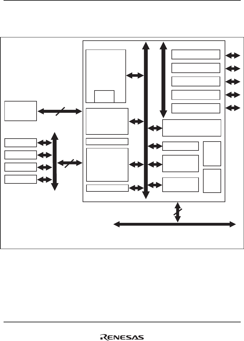
1. Overview
Rev.1.00 Jan. 10, 2008 Page 13 of 1658
REJ09B0261-0100
1.2 Block Diagram
A block diagram of the SH7785 is given as figure 1.1.
ROM
NOR Flash
PC Card/ATA3
DDR2-SDRAM
DDR2-400/600
1 GB max
SH-4A
Superscalar CPU
FPU
MMU
32 KB I-cache
32 KB O-cache
8 KB ILRAM
16 KB OLRAM
32 bit/16 bit
300 MHz
32 bit
33/66 MHz
PCI bus
64*/32/16
/8 bit
100 MHz Local Bus
Controller
SRAM, ROM,
PCMCIA
MPX
SCIF0/HSPI/FLCTL
Periperal busSuper Hyway
CPG
TMU, WDT
SRAM
PCI
Controller
HAC/SSI/SIOF
DMA
Controller
INTC
Debug
GDTA
SCIF2/MMCIF
Display Unit
Peripheral Bus Controller
DDR bus
Local bus
DDRII-SDRAM
Controller
(DBSC)
URAM
128 KB
HAC/SSI
Note: * The PCI bus and the display unit are not available when the local bus width is 64 bits.
The PCI controller and the display unit cannot be used when the local bus width is 64 bits.
Figure 1.1 SH7785 Block Diagram

1. Overview
Rev.1.00 Jan. 10, 2008 Page 14 of 1658
REJ09B0261-0100
1.3 Pin Arrangement Table
Table 1.2 Pin Function
No. Pin Name I/O Function No. Pin Name I/O Function
1 MDQ0 IO DDR data 0 28 MDQ27 IO DDR data 27
2 MDQ1 IO DDR data 1 29 MDQ28 IO DDR data 28
3 MDQ2 IO DDR data 2 30 MDQ29 IO DDR data 29
4 MDQ3 IO DDR data 3 31 MDQ30 IO DDR data 30
5 MDQ4 IO DDR data 4 32 MDQ31 IO DDR data 31
6 MDQ5 IO DDR data 5 33 MDM0 O DDR data mask 0
7 MDQ6 IO DDR data 6 34 MDM1 O DDR data mask 1
8 MDQ7 IO DDR data 7 35 MDM2 O DDR data mask 2
9 MDQ8 IO DDR data 8 36 MDM3 O DDR data mask 3
10 MDQ9 IO DDR data 9 37 MDQS0 IO DDR data strobe 0
11 MDQ10 IO DDR data 10 38 MDQS1 IO DDR data strobe 1
12 MDQ11 IO DDR data 11 39 MDQS2 IO DDR data strobe 2
13 MDQ12 IO DDR data 12 40 MDQS3 IO DDR data strobe 3
14 MDQ13 IO DDR data 13 41 MDQS0 IO DDR data strobe 0
(antiphase)
15 MDQ14 IO DDR data 14 42 MDQS1 IO DDR data strobe 1
(antiphase)
16 MDQ15 IO DDR data 15 43 MDQS2 IO DDR data strobe 2
(antiphase)
17 MDQ16 IO DDR data 16 44 MDQS3 IO DDR data strobe 3
(antiphase)
18 MDQ17 IO DDR data 17 45 MA0 O DDR address 0
19 MDQ18 IO DDR data 18 46 MA1 O DDR address 1
20 MDQ19 IO DDR data 19 47 MA2 O DDR address 2
21 MDQ20 IO DDR data 20 48 MA3 O DDR address 3
22 MDQ21 IO DDR data 21 49 MA4 O DDR address 4
23 MDQ22 IO DDR data 22 50 MA5 O DDR address 5
24 MDQ23 IO DDR data 23 51 MA6 O DDR address 6
25 MDQ24 IO DDR data 24 52 MA7 O DDR address 7
26 MDQ25 IO DDR data 25 53 MA8 O DDR address 8
27 MDQ26 IO DDR data 26 54 MA9 O DDR address 9

1. Overview
Rev.1.00 Jan. 10, 2008 Page 15 of 1658
REJ09B0261-0100
No. Pin Name I/O Function No. Pin Name I/O Function
55 MA10 O DDR address 10 87 D12 IO Local bus data 12
56 MA11 O DDR address 11 88 D13 IO Local bus data 13
57 MA12 O DDR address 12 89 D14 IO Local bus data 14
58 MA13 O DDR address 13 90 D15 IO Local bus data 15
59 MA14 O DDR address 14 91 D16 IO Local bus data 16
60 MBA0 O DDR bank address 0 92 D17 IO Local bus data 17
61 MBA1 O DDR bank address 1 93 D18 IO Local bus data 18
62 MBA2 O DDR bank address 2 94 D19 IO Local bus data 19
63 MCK0 O DDR clock 0 95 D20 IO Local bus data 20
64 MCK0 O DDR clock 0 (antiphase) 96 D21 IO Local bus data 21
65 MCK1 O DDR clock 1 97 D22 IO Local bus data 22
66 MCK1 O DDR clock 1 (antiphase) 98 D23 IO Local bus data 23
67 MCS O DDR chip select 99 D24 IO Local bus data 24
68 MRAS O DDR row address select 100 D25 IO Local bus data 25
69 MCAS O DDR column address select 101 D26 IO Local bus data 26
70 MWE O DDR write enable 102 D27 IO Local bus data 27
71 MODT O DDR on chip terminator 103 D28 IO Local bus data 28
72 MCKE O DDR clock enable 104 D29 IO Local bus data 29
73 MVREF I DDR reference voltage 105 D30 IO Local bus data 30
74 MBKPRST I DDR backup reset 106 D31 IO Local bus data 31
75 D0 IO Local bus data 0 107 A0 O Local bus address 0
76 D1 IO Local bus data 1 108 A1 O Local bus address 1
77 D2 IO Local bus data 2 109 A2 O Local bus address 2
78 D3 IO Local bus data 3 110 A3 O Local bus address 3
79 D4 IO Local bus data 4 111 A4 O Local bus address 4
80 D5 IO Local bus data 5 112 A5 O Local bus address 5
81 D6 IO Local bus data 6 113 A6 O Local bus address 6
82 D7 IO Local bus data 7 114 A7 O Local bus address 7
83 D8 IO Local bus data 8 115 A8 O Local bus address 8
84 D9 IO Local bus data 9 116 A9 O Local bus address 9
85 D10 IO Local bus data 10 117 A10 O Local bus address 10
86 D11 IO Local bus data 11 118 A11 O Local bus address 11

1. Overview
Rev.1.00 Jan. 10, 2008 Page 16 of 1658
REJ09B0261-0100
No. Pin Name I/O Function No. Pin Name I/O Function
119 A12 O Local bus address 12 140 RD/FRAME O/O Read strobe/MPX IF
FRAME
120 A13 O Local bus address 13 141 R/W O Read/Write
121 A14 O Local bus address 14 142 BS O Bus start
122 A15 O Local bus address 15 143 WE0/REG O/O Write enable 0/PCMCIA IF
REG
123 A16 O Local bus address 16 144 WE1 O Write enable 1
124 A17 O Local bus address 17 145 WE2/IORD O/O Write enable 2/PCMCIA IF
IORD
125 A18 O Local bus address 18 146 WE3/IOWR O/O Write enable 3/PCMCIA IF
IOWR
126 A19 O Local bus address 19 147 RDY I Bus ready
127 A20 O Local bus address 20 148 CLKOUT O Clock out
128 A21 O Local bus address 21 149 CLKOUTENB O Clock out enable
129 A22 O Local bus address 22 150 D32/AD0/DR0 IO/IO/O Local bus data 32/PCI
address data 0/Digital red 0
130 A23 O Local bus address 23 151 D33/AD1/DR1 IO/IO/O Local bus data 33/PCI
address data 1/Digital red 1
131 A24 O Local bus address 24 152 D34/AD2/DR2 IO/IO/O Local bus data 34/PCI
address data 2/Digital red 2
132 A25 O Local bus address 25 153 D35/AD3/DR3 IO/IO/O Local bus data 35/PCI
address data 3/Digital red 3
133 CS0 O Chip select 0 154 D36/AD4/DR4 IO/IO/O Local bus data 36/PCI
address data 4/Digital red 4
134 CS1 O Chip select 1 155 D37/AD5/DR5 IO/IO/O Local bus data 37/PCI
address data 5/Digital red 5
135 CS2 O Chip select 2 156 D38/AD6/DG0 IO/IO/O Local bus data 38/PCI
address data 6/Digital green
0
136 CS3 O Chip select 3 151 D33/AD1/DR1 IO/IO/O Local bus data 33/PCI
address data 1/Digital red 1
137 CS4 O Chip select 4 152 D34/AD2/DR2 IO/IO/O Local bus data 34/PCI
address data 2/Digital red 2
138 CS5 O Chip select 5 153 D35/AD3/DR3 IO/IO/O Local bus data 35/PCI
address data 3/Digital red 3
139 CS6 O Chip select 6 154 D36/AD4/DR4 IO/IO/O Local bus data 36/PCI
address data 4/Digital red 4

1. Overview
Rev.1.00 Jan. 10, 2008 Page 17 of 1658
REJ09B0261-0100
No. Pin Name I/O Function No. Pin Name I/O Function
155 D37/AD5/DR5 IO/IO/O Local bus data 37/PCI
address data 5/Digital red 5
168 D50/AD18 IO/IO Local bus data 50/PCI
address data 18
156 D38/AD6/DG0 IO/IO/O Local bus data 38/PCI
address data 6/Digital green
0
169 D51/AD19 IO/IO Local bus data 51/PCI
address data 19
157 D39/AD7/DG1 IO/IO/O Local bus data 39/PCI
address data 7/Digital green
1
170 D52/AD20 IO/IO Local bus data 52/PCI
address data 20
158 D40/AD8/DG2 IO/IO/O Local bus data 40/PCI
address data 8/Digital green
2
171 D53/AD21 IO/IO Local bus data 53/PCI
address data 21
159 D41/AD9/DG3 IO/IO/O Local bus data 41/PCI
address data 9/Digital green
3
172 D54/AD22 IO/IO Local bus data 54/PCI
address data 22
160 D42/AD10/DG4 IO/IO/O Local bus data 42/PCI
address data 10/Digital
green 4
173 D55/AD23 IO/IO Local bus data 55/PCI
address data 23
161 D43/AD11/DG5 IO/IO/O Local bus data 43/PCI
address data 11/Digital
green 5
174 D56/AD24 IO/IO Local bus data 56/PCI
address data 24
162 D44/AD12/DB0 IO/IO/O Local bus data 44/PCI
address data 12/Digital blue
0
175 D57/AD25 IO/IO Local bus data 57/PCI
address data 25
163 D45/AD13/DB1 IO/IO/O Local bus data 45/PCI
address data 13/Digital blue
1
176 D58/AD26 IO/IO Local bus data 58/PCI
address data 26
164 D46/AD14/DB2 IO/IO/O Local bus data 46/PCI
address data 14/Digital blue
2
177 D59/AD27 IO/IO Local bus data 59/PCI
address data 27
165 D47/AD15/DB3 IO/IO/O Local bus data 47/PCI
address data 15/Digital blue
3
178 D60/AD28 IO/IO Local bus data 60/PCI
address data 28
166 D48/AD16/DB4 IO/IO/O Local bus data 48/PCI
address data 16/Digital blue
4
179 D61/AD29 IO/IO Local bus data 61/PCI
address data 29
167 D49/AD17/DB5 IO/IO/O Local bus data 49/PCI
address data 17/Digital blue
5
180 D62/AD30 IO/IO Local bus data 62/PCI
address data 30

1. Overview
Rev.1.00 Jan. 10, 2008 Page 18 of 1658
REJ09B0261-0100
No. Pin Name I/O Function No. Pin Name I/O Function
181 D63/AD31 IO/IO Local bus data 63/PCI
address data 31
199 REQ2 I Bus request 2 (PCI host)
182 WE4/CBE0 O/IO Write enable 4/PCI
command/byte enable 0
200 REQ3 I Bus request 3 (PCI host)
183 WE5/CBE1 O/IO Write enable 5/PCI
command/byte enable 1
201 GNT1 O PCI bus grant 1
184 WE6/CBE2 O/IO Write enable 6/PCI
command/byte enable 2
202 GNT2 O PCI bus grant 2
185 WE7/CBE3 O/IO Write enable 7/PCI
command/byte enable 3
203 GNT3/MMCCLK O/O PCI bus grant 3/MMCIF card
clock output
186 PCIFRAME/
VSYNC
IO/IO PCI cycle frame/VSYNC
output
204 PCIRESET O PCI reset (RST)
187 IRDY/HSYNC IO/IO PCI initiator ready/HSYNC
output
205 PCICLK/
DCLKIN
I/I PCI input clock/DU dot clock
input
188 TRDY/DISP IO/O PCI target ready/display
period
206 INTA IO PCI interrupt A
189 IDSEL I PCI configuration device
select
207 EXTAL I External input clock/Crystal
resonator
190 LOCK/ODDF IO/IO PCI lock/even-odd field 208 XTAL O Crystal resonator
191 DEVSEL/
DCLKOUT
IO/O PCI device select/DU dot
clock output
209 PRESET I Power on reset
192 PAR IO PCI parity 210 NMI I Nonmaskable interrupt
193 STOP/CDE IO/O PCI transaction stop/color
detection
211 IRL0 I IRL interrupt request 0
194 SERR IO PCI system error 212 IRL1 I IRL interrupt request 1
195 PERR IO PCI parity error 213 IRL2 I IRL interrupt request 2
196 REQ0/REQOUT I/O Bus request 0 (PCI host)/
bus request output
214 IRL3 I IRL interrupt request 3
197 GNT0/GNTIN O/I PCI bus grant 0 215 STATUS0/
DRAK0
O/O Status 0/DMA channel 0
transfer request
acknowledge 0
198 REQ1 I PCI request 1 (PCI host) 216 STATUS1/
DRAK1
O/O Status 1/DMA channel 1
transfer request
acknowledge 1

1. Overview
Rev.1.00 Jan. 10, 2008 Page 19 of 1658
REJ09B0261-0100
No. Pin Name I/O Function No. Pin Name I/O Function
217 BREQ/BSACK I Bus request (Master mode)/
Bus acknowledgement
(Slave mode)
233 ASEBRK/
BRKACK
I H-UDI emulator
218 BACK/BSREQ O Bus acknowledgement
(Master mode)/Bus request
(Slave mode)
234 AUDCK O H-UDI emulator clock
219 DREQ0 I DMA channel 0 request 235 AUDSYNC O H-UDI emulator
220 DREQ1 I DMA channel 1 request 236 AUDATA0 O H-UDI emulator data 0
221 DREQ2/INTB I/I DMA channel 2 request/PCI
interrupt B
237 AUDATA1 O H-UDI emulator data 1
222 DREQ3/INTC I/I DMA channel 3 request/PCI
interrupt C
238 AUDATA2 O H-UDI emulator data 2
223 DACK0 O DMA channel 0 bus
acknowledgment
239 AUDATA3 O H-UDI emulator data 3
224 DACK1 O DMA channel 1 bus
acknowledgment
240 SCIF0_TXD/
HSPI_TX/FWE
O/O/O SCIF0 transmit data/HSPI
transmit data/NAND flash
write enable
225 DACK2/
SCIF2_TXD/
MMCCMD/
SIOF_TXD
O/O/O/I
O/O
DMA channel 2 bus
acknowledgment/SCIF2
transmit data/MMCIF
command response/SIOF
transmit data
241 SCIF0_RXD/
HSPI_RX/FRB
I/I/I SCIF0 receive data/HSPI
receive data/NAND flash
ready or busy
226 DACK3/
SCIF2_SCK/
MMCDAT/
SIOF_SCK
O/O/IO/
IO/IO
DMA channel 3 bus
acknowledgment/SCIF2
serial clock/MMCIF
data/SIOF serial clock
242 SCIF0_SCK/
HSPI_CLK/FRE
IO/IO/O SCIF0 serial clock/HSPI
serial clock/NAND flash read
enable
227 DRAK2/CE2A O/O DMA channel 2 transfer
request acknowledge
2/PCMCIA CE2A
243 SCIF0_RTS/
HSPI_CS/FSE
IO/IO/O SCIF0 modem control/HSPI
chip selection/NAND flash
spare area enable
228 TCK I H-UDI clock 244 SCIF0_CTS/
INTD/FCE
IO/I/O SCIF0 modem control/PCI
interrupt D/NAND flash chip
enable
229 TMS I H-UDI emulator 245 SCIF1_TXD O SCIF1 transmit data
230 TDI I H-UDI data 246 SCIF1_RXD I SCIF1 receive data
231 TDO O H-UDI data 247 SCIF1_SCK IO SCIF1 serial clock
232 TRST I H-UDI emulator 248 SCIF2_RXD/
SIOF_RXD
I/I SCIF2 receive data/SIOF
receive data

1. Overview
Rev.1.00 Jan. 10, 2008 Page 20 of 1658
REJ09B0261-0100
No. Pin Name I/O Function No. Pin Name I/O Function
249 SIOF_SCK/
HAC0_BITCLK/
SSI0_CLK
IO/I/IO SIOF serial clock/HAC0 bit
clock/SSI0 serial bit clock
256 SCIF5_RXD/
HAC1_SDIN/
SSI1_SCK
I/I/IO SCIF5 receive data/HAC1
serial data/SSI1 serial data
250 SIOF_MCLK/
HAC_RES
I/O SIOF master clock/HAC
reset
257 SCIF5_SCK/
HAC1_SDOUT/
SSI1_SDATA
IO/O/IO SCIF5 synchrounous/HAC1
serial data/SSI1 serial data
251 SIOF_SYNC/
HAC0_SYNC/
SSI0_WS
IO/O/IO SIOF flame
synchronous/HAC0 flame
synchronous/SSI0 word
select
258 MODE0/
IRL4/FD4
I/I/IO Mode control 0/IRL interrupt
request 4/NAND flash data 4
252 SIOF_RXD/
HAC0_SDIN/
SSI0_SCK
I/I/IO SIOF receive data/HAC0
serial data incoming to Rx
frame/SSI0 serial bit clock
259 MODE1/
IRL5/FD5
I/I/IO Mode control 1/IRL interrupt
request 5/NAND flash data 5
253 SIOF_TXD/
HAC0_SDOUT/
SSI0_SDATA
O/O/IO SIOF transmit data/HAC0
serial data/SSI0 serial data
260 MODE2/
IRL6/FD6
I/I/IO Mode control 2/IRL interrupt
request 6/NAND flash data 6
254 HAC1_BITCLK/
SSI1_CLK
I/IO HAC1 bit clock/SSI1 serial
bit clock
261 MODE3/
IRL7/FD7
I/I/IO Mode control 3/IRL interrupt
request 7/NAND flash data 7
255 SCIF5_TXD/
HAC1_SYNC/
SSI1_WS
O/O/IO SCIF5 transmit data/HAC1
synchronous/SSI1 serial bit
clock
262 MODE4/
SCIF3_TXD/
FCLE
I/O/O Mode control 4/SCIF3
transmit data/NAND flash
command latch enable
256 SCIF5_RXD/
HAC1_SDIN/
SSI1_SCK
I/I/IO SCIF5 receive data/HAC1
serial data/SSI1 serial data
263 MODE5/
SIOF_MCLK
I/I Mode control 5/SIOF master
clock
251 SIOF_SYNC/
HAC0_SYNC/
SSI0_WS
IO/O/IO SIOF flame
synchronous/HAC0 flame
synchronous/SSI0 word
select
264 MODE6/
SIOF_SYNC
I/IO Mode control 6/SIOF frame
synchronous
252 SIOF_RXD/
HAC0_SDIN/
SSI0_SCK
I/I/IO SIOF receive data/HAC0
serial data incoming to Rx
frame/SSI0 serial bit clock
265 MODE7/
SCIF3_RXD/
FALE
I/I/O Mode control 7/SCIF3
receive data/NAND flash
ALE
253 SIOF_TXD/
HAC0_SDOUT/
SSI0_SDATA
O/O/IO SIOF transmit data/HAC0
serial data/SSI0 serial data
266 MODE8/
SCIF3_SCK/
FD0
I/IO/IO Mode control 8/SCIF3 serial
clock/NAND flash data 0
254 HAC1_BITCLK/
SSI1_CLK
I/IO HAC1 bit clock/SSI1 serial
bit clock
267 MODE9/
SCIF4_TXD/
FD1
I/O/IO Mode control 9/SCIF4
transmit data/NAND flash
data 1
255 SCIF5_TXD/
HAC1_SYNC/
SSI1_WS
O/O/IO SCIF5 transmit data/HAC1
synchronous/SSI1 serial bit
clock
268 MODE10/
SCIF4_RXD/
FD2
I/I/IO Mode control 10/SCIF4
receive data/NAND flash
data 2

1. Overview
Rev.1.00 Jan. 10, 2008 Page 21 of 1658
REJ09B0261-0100
No. Pin Name I/O Function No. Pin Name I/O Function
269 MODE11/
SCIF4_SCK/
FD3
I/IO/IO Mode control 11/SCIF4
serial clock/NAND flash data
3
274 MRESETOUT/
IRQOUT
O/O Manual reset
output/Interrupt request
output
270 MODE12/
DRAK3/CE2B
I/O/O Mode control 12/DMA
channel 3 transfer request
acknowledge 3/PCMCIA
CE2B
275 THDAG ⎯ Thermal diode*
271 MODE13/
TCLK/IOIS16
I/IO/I TMU clock/PCMCIA IOIS16 276 THDAS ⎯ Thermal diode*
272 MPMD I H-UDI emulator mode 277 THDCD I Thermal diode*
273 MODE14 I Mode control 14 278 THDCTL I Thermal diode*
Note: * This pin must be pulled-down to GND.

1. Overview
Rev.1.00 Jan. 10, 2008 Page 22 of 1658
REJ09B0261-0100
1.4 Pin Arrangement
Package: 436-pin FC-BGA, 19 mm x 19 mm, ball pitch: 0.8 mm
A
B
C
D
E
F
G
H
J
K
L
M
N
P
R
T
U
V
W
Y
AA
A
B
C
D
E
F
G
H
J
K
L
M
N
P
R
T
U
V
W
Y
AA
AB AB
12345678910111213141516171819202122
12345678910111213141516171819202122
VSS
MCK1
VSS
MVREF
MA10
MA14
MDQ22
MDQ16
MDQ28
MDQ26
MDM3
VSS
PRESET
SCIF0_SCK
/HSPI_CLK
/FRE
SCIF1_
SCK
SCIF1_
TXD
SIOF_TXD/
HAC0_SDO
UT/SSI0_
SDATA
SIOF_MCLK
/HAC_RES
SCIF5_SCK
/HAC1_SD
OUT/SSI1_
SDATA
SCIF5_TXD
/HAC1_
SYNC/
SSI1_WS
A25
VSS
MCK0
VDD-
DDR
MCK1
VDD-
DDR
MCS
VSS
MDQ17
VDD-
DDR
MDQ23
VSS
MDQ31
VSS
VSS
SCIF0_TXD
/HSPI_TX/
FWE
VDDQ
SCIF1_
RXD
VSS
SIOF_SYNC
/HAC0_
SYNC/SSI0_
WS
VDDQ
SCIF5_RXD
/HAC1_
SDIN/SSI1_
SCK
VDDQ
A24
VSS
MCK0
MBKPRST
MBA1
MCAS
MA6
MDQ21
MDQ18
MDQS
2
MDQ25
MDQS
3
MODE0
/IRL4
/FD4
MODE1
/IRL5
/FD5
SCIF0_RXD
/HSPI_RX/
FRB
MODE5/
SIOF_MCLK
MODE6/SI
OF_SYNC
SIOF_SCK
/HAC0_BIT
CLK/SSI0_
CLK
HAC1_BI
TCLK/
SSI1_CLK
MODE11
/SCIF4_S
CK/FD3
A23
A22
A21
MCKE
VDD-
DDR
MODT
VSS
MRAS
VDD-
DDR
MA8
VSS
MDQS2
VDD-
DDR
MDQS3
VDDQ
MODE2
/IRL6
/FD6
SCIF0_CTS
/INTD/
FCE
VSS
SIOF_RXD
/HAC0_
SDIN/SSI0_
SCK
VDDQ
MODE9/
SCIF4_
TXD/FD1
VSS
A20
VDDQ
A19
MBA0
MA1
MBA2
MA2
MWE
MA0
MA4
MDQ19
MDM2
MDQ27
MDQ29
VDD-
DDR
MODE3
/IRL7
/FD7
SCIF0_RTS
/HSPI_CS
/FSE
MODE8/
SCIF3_
SCK/FD0
MODE10/
SCIF4_RXD
/FD2
CS6
CS5
A18
A17
A16
A15
MA9
VSS
MA11
VDD-
DDR
MA5
VSS
MA12
VDD-
DDR
MDQ20
VSS
MDQ30
MDQ24
VSS
MODE7/
SCIF3_
RXD/FALE
MODE4/
SCIF3_
TXD/FCLE
VDDQ
VSS
A14
VDDQ
A13
VSS
A12
MDQ1
MDQ2
MDQ4
MA13
MA3
MA7
VSS
VDD
VSS
VDD
VSS
VDD
VSS
VDD
VSS
VDD
CS4
A11
A10
A9
A8
A7
MDQ7
VDD-
DDR
MDQ0
VSS
MDQ3
VDD-
DDR
VDD
VSS
VDDQ
A6
VSS
A5
VDDQ
A4
MDQ13
MDQ6
MDQS
0
MDQS0
MDM0
MDQ5
VSS
VDD
R/W
CS3
A3
A2
A1
A0
MDQ12
VSS
MDQ10
VDD-
DDR
MDQ11
VSS
VDD
VSS
VSS
VSS
VSS
VSS
VSS
CS2
VDDQ
D1
VSS
D0
MDM1
MDQ14
MDQS
1
MDQS1
MDQ15
MDQ8
VSS
VSS
VSS
VSS
VSS
VDD
RD/F
RAME
CS1
CS0
D4
D3
D2
AUDSYNC
AUDAT
A2
AUDAT
A0
AUDAT
A1
VDD-
DDR
MDQ9
VDD
VSS
VSS
VSS
VSS
VSS
D12
D8
WE0/
REG
D7
D6
D5
AUDC
K
VSS
AUDAT
A3
VDDQ
TDO
VSS
VSS
VSS
VSS
VSS
VSS
VDD
VSS
D11
VDDQ
D10
VSS
D9
TCK
TDI
ASEBRK
/BRKACK
THDAG
THDAS
THDCD
VDD
VSS
MODE13
/TCLK/
IOIS16
D16
WE1
D15
D14
D13
VSSQ-
TD
VDDQ
TRST
VSS
TMS
VDDQ
VSS
VDD
VDDQ
BS
VSS
D18
VDDQ
D17
THDCTL
VDDQ-
TD
DACK0
DREQ1
DACK1
DRAK2
/CE2A
VDD
VSS
VDD
VSS
VDD
VSS
VDD
VSS
VDD
VSS
RDY
BACK/
BSREQ
D22
D21
D20
D19
STATU
S1/DRA
K1
VSS
DREQ0
VDDQ
DREQ2
/INTB
VSS
IRL3
VDDQ
IRL0
VSS
WE5/
CBE1
DEVSEL/
DCLKOUT
VSS
D52/A
D20
VDDQ
REQ0/
REQOUT
VSS
BREQ/
BSACK
VDDQ
WE2/
IORD
VSS
D23
XTAL
STATUS0/
DRAK0
MPMD
SCIF2_RXD
/SIOF_RXD
DACK2/
SCIF2_TXD/
MMCCMD/
SIOF_TXD
MRESETO
UT/
IRQOUT
IRL1
D35/AD3/
DR3
WE4/
CBE0
D42/AD
10/DG4
D47/AD
15/DB3
STOP
/CDE
PCIFRA
ME/VS
YNC
D51/A
D19
D55/A
D23
D58/A
D26
REQ1
REQ2
D27
D26
D25
D24
EXTAL
VDDQ
NMI
VSS
DACK3/
SCIF2_SCK/
MMCDAT/
SIOF_SCK
VDDQ
IRL2
VSS
D39/AD
7/DG1
VDDQ
D46/AD
14/DB2
LOCK
/ODDF
VDDQ
D50/A
D18
VSS
D57/A
D25
VDDQ
D63/A
D31
VSS
D29
VDDQ
D28
MODE14
VDDQ
-PLL1
VDDA-
PLL1
VDDQ
-PLL2
DREQ3
/INTC
CLKOU
TENB
MODE12/
DRAK3/
CE2B
D34/AD
2/DR2
D38/AD
6/DG0
D41/AD
9/DG3
D45/AD
13/DB1
PERR
IRDY/
HSYNC
D49/AD
17/DB5
D54/A
D22
D56/A
D24
D60/A
D28
D62/A
D30
GNT0/
GNTIN
GNT2
D31
D30
VSSQ-
PLL1
VDDQ
VDD-
PLL1
VDDQ
VDD-
PLL2
VSS
INTA
VDDQ
D37/AD
5/DR5
VSS
D44/AD
12/DB0
SERR
VSS
D48/AD
16/DB4
VDDQ
WE7/
CBE3
VSS
D61/A
D29
VDDQ
GNT1
VDDQ
WE3/I
OWR
VSS
VSSA-
PLL1
VSS-
PLL1
VSSQ-
PLL2
VSS-
PLL2
CLKO
UT
D32/AD
0/DR0
D33/AD
1/DR1
D36/AD
4/DR4
D40/AD
8/DG2
D43/AD
11/DG5
PAR
TRDY
/DISP
WE6/
CBE2
D53/A
D21
IDSEL
D59/A
D27
PCICLK
/DCLKIN
REQ3
PCIRES
ET
GNT3/
MMCCLK
VSS
PKG TOP VIEW
Figure 1.2 SH7785 Pin Arrangement (Top View)
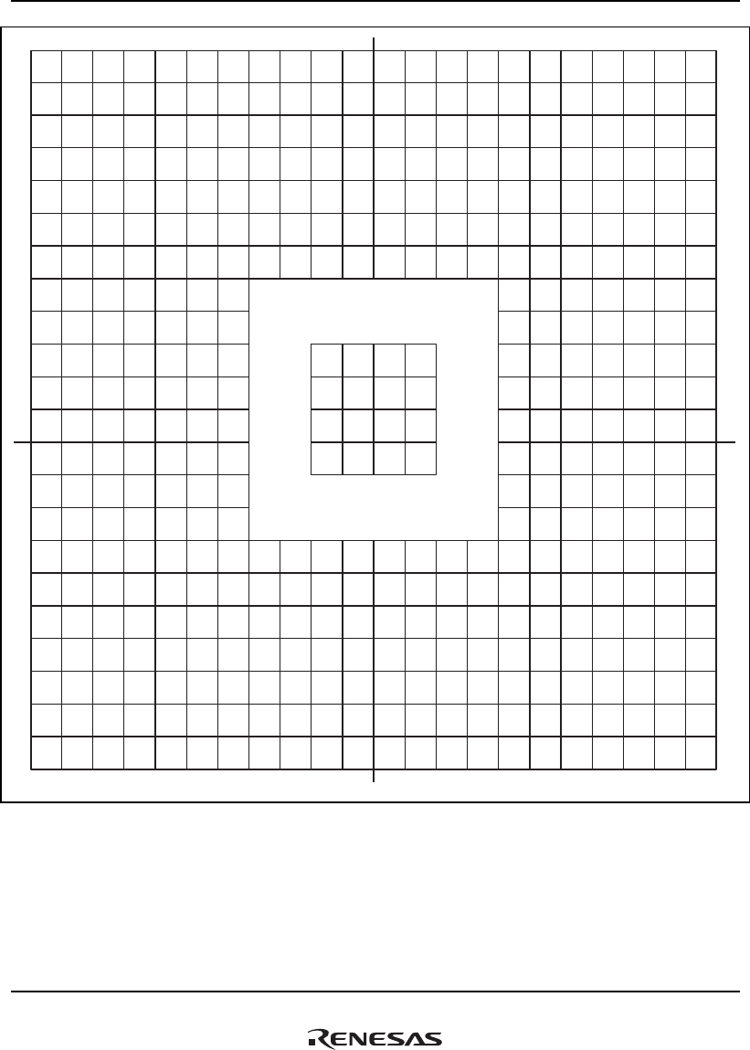
1. Overview
Rev.1.00 Jan. 10, 2008 Page 23 of 1658
REJ09B0261-0100
12345678910111213141516171819202122
12345678910111213141516171819202122
VSS
A25
SCIF5_TXD
/HAC1_
SYNC/SSI1_
WS
SCIF5_SCK
/HAC1_SD
OUT/SSI1_
SDATA
SIOF_MCLK
/HAC_RES
SIOF_TXD/
HAC0_SDO
UT/SSI0_
SDATA
SCIF1_
TXD
SCIF1_
SCK
SCIF0_SCK
/HSPI_CLK
/FRE
PRESET
VSS
MDM3
MDQ26
MDQ28
MDQ16
MDQ22
MA14
MA10
MVRE
F
VSS
MCK1
VSS
A24
VDDQ
SCIF5_RXD
/HAC1_
SDIN/SSI1_
SCK
VDDQ
SIOF_SYNC
/HAC0_
SYNC/
SSI0_WS
VSS
SCIF1_
RXD
VDDQ
SCIF0_TXD
/HSPI_TX/
FWE
VSS
VSS
MDQ31
VSS
MDQ23
VDD-
DDR
MDQ17
VSS
MCS
VDD-
DDR
MCK1
VDD-
DDR
MCK0
A21
A22
A23
MODE11/
SCIF4_SCK
/FD3
HAC1_BIT
CLK/SSI1_
CLK
SIOF_SCK
/HAC0_BIT
CLK/SSI0_
CLK
MODE6/
SIOF_SYNC
MODE5/
SIOF_MCLK
SCIF0_RXD
/HSPI_RX/
FRB
MODE1/
IRL5/FD5
MODE0
/IRL4/
FD4
MDQS
3
MDQ25
MDQS
2
MDQ18
MDQ21
MA6
MCAS
MBA1
MBKPRST
MCK0
VSS
A19
VDDQ
A20
VSS
MODE9/S
CIF4_TXD/
FD1
VDDQ
SIOF_RXD
/HAC0_SDI
N/SSI0_
SCK
VSS
SCIF0_CTS
/INTD/F
CE
MODE2/
IRL6/FD6
VDDQ
MDQS3
VDD-
DDR
MDQS2
VSS
MA8
VDD-
DDR
MRAS
VSS
MODT
VDD-
DDR
MCKE
A15
A16
A17
A18
CS5
CS6
MODE10/
SCIF4_RXD
/FD2
MODE8/
SCIF3_SCK/
FD0
SCIF0_RTS
/HSPI_CS
/FSE
MODE3/
IRL7/FD7
VDD-
DDR
MDQ29
MDQ27
MDM2
MDQ19
MA4
MA0
MWE
MA2
MBA2
MA1
MBA0
A12
VSS
A13
VDDQ
A14
VSS
VDDQ
MODE4/
SCIF3_TXD/
FCLE
MODE7/S
CIF3_RXD/
FALE
VSS
MDQ24
MDQ30
VSS
MDQ20
VDD-
DDR
MA12
VSS
MA5
VDD-
DDR
MA11
VSS
MA9
A7
A8
A9
A10
A11
CS4
VDD
VSS
VDD
VSS
VDD
VSS
VDD
VSS
VDD
VSS
MA7
MA3
MA13
MDQ4
MDQ2
MDQ1
A4
VDDQ
A5
VSS
A6
VDDQ
VSS
VDD
VDD-
DDR
MDQ3
VSS
MDQ0
VDD-
DDR
MDQ7
A0
A1
A2
A3
CS3
R/W
VDD
VSS
MDQ5
MDM0
MDQS0
MDQS
0
MDQ6
MDQ13
D0
VSS
D1
VDDQ
CS2
VSS
VSS
VSS
VSS
VSS
VSS
VDD
VSS
MDQ11
VDD-
DDR
MDQ10
VSS
MDQ12
D2
D3
D4
CS0
CS1
RD/
FRAME
VDD
VSS
VSS
VSS
VSS
VSS
MDQ8
MDQ15
MDQS1
MDQS
1
MDQ14
MDM1
D5
D6
D7
WE0/
REG
D8
D12
VSS
VSS
VSS
VSS
VSS
VDD
MDQ9
VDD-
DDR
AUDA
TA1
AUDA
TA0
AUDA
TA2
AUDSY
NC
D9
VSS
D10
VDDQ
D11
VSS
VDD
VSS
VSS
VSS
VSS
VSS
VSS
TDO
VDDQ
AUDA
TA3
VSS
AUDCK
D13
D14
D15
WE1
D16
MODE13
/TCLK/
IOIS16
VSS
VDD
THDCD
THDAS
THDAG
ASEBRK/
BRKACK
TDI
TCK
D17
VDDQ
D18
VSS
BS
VDDQ
VDD
VSS
VDDQ
TMS
VSS
TRST
VDDQ
VSSQ-
TD
D19
D20
D21
D22
BACK/
BSREQ
RDY
VSS
VDD
VSS
VDD
VSS
VDD
VSS
VDD
VSS
VDD
DRAK2
/CE2A
DACK1
DREQ1
DACK0
VDDQ-
TD
THDCTL
D23
VSS
WE2/
IORD
VDDQ
BREQ/
BSACK
VSS
REQ0/
REQOUT
VDDQ
D52/A
D20
VSS
DEVSE
L/DC
LKOUT
WE5/
CBE1
VSS
IRL0
VDDQ
IRL3
VSS
DREQ2
/INTB
VDDQ
DREQ0
VSS
STATUS1
/DRAK1
D24
D25
D26
D27
REQ2
REQ1
D58/A
D26
D55/A
D23
D51/A
D19
PCIFRA
ME/VS
YNC
STOP
/CDE
D47/AD
15/DB3
D42/AD
10/DG4
WE4/
CBE0
D35/AD
3/DR3
IRL1
MRESET
OUT/
IRQOUT
DACK2/S
CIF2_TXD/
MMCCMD/
SIOF_TXD
SCIF2_RXD
/SIOF_RXD
MPMD
STATUS0
/DRAK0
XTAL
D28
VDDQ
D29
VSS
D63/A
D31
VDDQ
D57/A
D25
VSS
D50/A
D18
VDDQ
LOCK
/ODDF
D46/AD
14/DB2
VDDQ
D39/AD
7/DG1
VSS
IRL2
VDDQ
DACK3/S
CIF2_SCK/
MMCDAT/
SIOF_SCK
VSS
NMI
VDDQ
EXTAL
D30
D31
GNT2
GNT0
/GNTIN
D62/A
D30
D60/A
D28
D56/A
D24
D54/A
D22
D49/A
D17/D
B5
IRDY/
HSYNC
PERR
D45/AD
13/DB1
D41/AD
9/DG3
D38/AD
6/DG0
D34/AD
2/DR2
MODE12
/DRAK3/
CE2B
CLKO
UTENB
DREQ3
/INTC
VDDQ
-PLL2
VDDA-
PLL1
VDDQ
-PLL1
MODE14
WE3/
IOWR
VDDQ
GNT1
VDDQ
D61/A
D29
VSS
WE7/
CBE3
VDDQ
D48/A
D16/D
B4
VSS
SERR
D44/AD
12/DB0
VSS
D37/AD
5/DR5
VDDQ
INTA
VSS
VDD-
PLL2
VDDQ
VDD-
PLL1
VDDQ
VSSQ-
PLL1
VSS
GNT3
/MMC
CLK
PCIRE
SET
REQ3
PCICLK
/DCLKIN
D59/A
D27
IDSEL
D53/A
D21
WE6/
CBE2
TRDY
/DISP
PAR
D43/AD
11/DG5
D40/AD
8/DG2
D36/AD
4/DR4
D33/AD
1/DR1
D32/AD
0/DR0
CLKOU
T
VSS-
PLL2
VSSQ-
PLL2
VSS-
PLL1
VSSA-
PLL1
VSS
PKG BTM VIEW
AB
AA
Y
W
V
U
T
R
P
N
M
L
K
J
H
G
F
E
D
C
B
AB
AA
Y
W
V
U
T
R
P
N
M
L
K
J
H
G
F
E
D
C
B
A A
Figure 1.3 SH7785 Pin Arrangement (Bottom View)
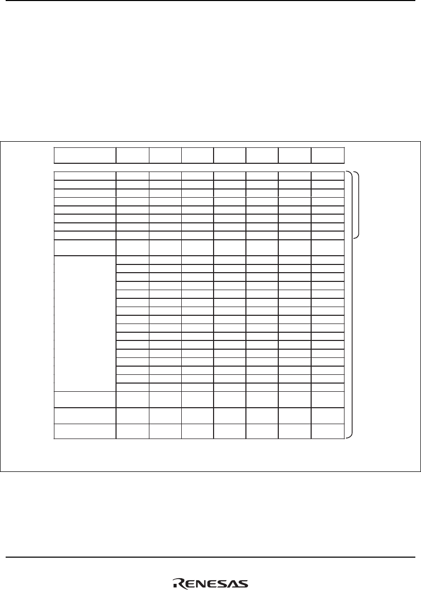
1. Overview
Rev.1.00 Jan. 10, 2008 Page 24 of 1658
REJ09B0261-0100
1.5 Physical Memory Address Map
The SH7785 supports 32-bit virtual address space, and supports both 29-bit and 32-bit physical
address spaces. For details of mappings from the virtual address space to the physical address
spaces, see section 7, Memory Management Unit (MMU).
Figure 1.4 shows the relationship between the AREASEL bits and the physical memory address
map. The 32-bit physical address space corresponds with the address space of the SuperHyway
bus.
MMSELR
AREASEL[2:0]* B'000 B'001 B'010 B'011 B'100 B'101 B'110
Area 0 LBSC LBSC LBSC LBSC LBSC LBSC LBSC
Area 1 LBSC LBSC LBSC LBSC LBSC LBSC LBSC
Area 2 LBSC LBSC DBSC2 DBSC2 DBSC2 LBSC LBSC
Area 3 DBSC3 DBSC3 DBSC3 DBSC3 DBSC3 LBSC LBSC
Area 4 LBSC PCIC LBSC PCIC DBSC4 LBSC PCIC
Area 5 LBSC LBSC LBSC LBSC DBSC5 LBSC LBSC
Area 6 LBSC LBSC LBSC LBSC LBSC LBSC LBSC
Area 7(Reserved)
(Undefined)
DBSC0 DBSC0 DBSC0 DBSC0 DBSC0 DBSC0 DBSC0
DBSC1
DBSC1
DBSC1
DBSC1
DBSC1
DBSC1
DBSC1
DBSC2
DBSC2
DBSC2
DBSC2
DBSC2
DBSC2
DBSC2
DBSC3
DBSC3
DBSC3
DBSC3
DBSC3
DBSC3
DBSC3
DBSC4
DBSC4
DBSC4
DBSC4
DBSC4
DBSC4
DBSC4
DBSC5
DBSC5
DBSC5
DBSC5
DBSC5
DBSC5
DBSC5
DBSC6
DBSC6
DBSC6
DBSC6
DBSC6
DBSC6
DBSC6
DBSC7
DBSC7
DBSC7
DBSC7
DBSC7
DBSC7
DBSC7
DBSC8
DBSC8
DBSC8
DBSC8
DBSC8
DBSC8
DBSC8
DBSC9
DBSC9
DBSC9
DBSC9
DBSC9
DBSC9
DBSC9
DBSC10
DBSC10 DBSC10 DBSC10 DBSC10 DBSC10 DBSC10
DBSC11
DBSC 11 DBSC11 DB SC11 DB SC11 DB SC11 DBSC11
DBSC12
DBSC12 DBSC12 DBSC12 DBSC12 DBSC12 DBSC12
DBSC13
DBSC13 DBSC13 DBSC13 DBSC13 DBSC13 DBSC13
DBSC14
DBSC14 DBSC14 DBSC14 DBSC14 DBSC14 DBSC14
DDR-SDRAM
DBSC15
DBSC15 DBSC15 DBSC15 DBSC15 DBSC15 DBSC15
(undefined)
PCI (PCIC) PCIC PCIC PCIC PCIC PCIC PCIC PCIC
(Internal resource)
H'0000 0000
H'0400 0000
H'0800 0000
H'0C00 0000
H'1000 0000
H'1400 0000
H'1800 0000
H'1C00 0000
H'2000 0000
H'4000 0000
H'4400 0000
H'4800 0000
H'4C00 0000
H'5000 0000
H'5400 0000
H'5800 0000
H'5C00 0000
H'6000 0000
H'6400 0000
H'6800 0000
H'6C00 0000
H'7000 0000
H'7400 0000
H'7800 0000
H'7C00 0000
H'8000 0000
H'C000 0000
H'E000 0000
H'FFFF FFFF
Note: Memory Address Map Select Register (MMSELR) Area Select Bit (AREASEL)
For details, refer to section 11.4.1, Memory Address Map Select Register (MMSELR).
32-bit physical
address space
(extended mode)
29-bit physical
address space
Figure 1.4 Relationship between AREASEL Bits and Physical Memory Address Map

2. Programming Model
Rev.1.00 Jan. 10, 2008 Page 25 of 1658
REJ09B0261-0100
Section 2 Programming Model
The programming model of this LSI is explained in this section. This LSI has registers and data
formats as shown below.
2.1 Data Formats
The data formats supported in this LSI are shown in figure 2.1.
Byte (8 bits)
Word (16 bits)
Longword (32 bits)
Single-precision floating-point (32 bits)
Double-precision floating-point (64 bits)
07
015
031
031 30 22
se f
063 62 51
se f
Legend:
s
e
f
:Sign field
:Exponent field
:Fraction field
Figure 2.1 Data Formats

2. Programming Model
Rev.1.00 Jan. 10, 2008 Page 26 of 1658
REJ09B0261-0100
2.2 Register Descriptions
2.2.1 Privileged Mode and Banks
(1) Processing Modes
This LSI has two processing modes, user mode and privileged mode. This LSI normally operates
in user mode, and switches to privileged mode when an exception occurs or an interrupt is
accepted. There are four kinds of registers—general registers, system registers, control registers,
and floating-point registers—and the registers that can be accessed differ in the two processing
modes.
(2) General Registers
There are 16 general registers, designated R0 to R15. General registers R0 to R7 are banked
registers which are switched by a processing mode change.
• Privileged mode
In privileged mode, the register bank bit (RB) in the status register (SR) defines which banked
register set is accessed as general registers, and which set is accessed only through the load
control register (LDC) and store control register (STC) instructions.
When the RB bit is 1 (that is, when bank 1 is selected), the 16 registers comprising bank 1
general registers R0_BANK1 to R7_BANK1 and non-banked general registers R8 to R15 can
be accessed as general registers R0 to R15. In this case, the eight registers comprising bank 0
general registers R0_BANK0 to R7_BANK0 are accessed by the LDC/STC instructions.
When the RB bit is 0 (that is, when bank 0 is selected), the 16 registers comprising bank 0
general registers R0_BANK0 to R7_BANK0 and non-banked general registers R8 to R15 can
be accessed as general registers R0 to R15. In this case, the eight registers comprising bank 1
general registers R0_BANK1 to R7_BANK1 are accessed by the LDC/STC instructions.
• User mode
In user mode, the 16 registers comprising bank 0 general registers R0_BANK0 to R7_BANK0
and non-banked general registers R8 to R15 can be accessed as general registers R0 to R15.
The eight registers comprising bank 1 general registers R0_BANK1 to R7_BANK1 cannot be
accessed.
(3) Control Registers
Control registers comprise the global base register (GBR) and status register (SR), which can be
accessed in both processing modes, and the saved status register (SSR), saved program counter
(SPC), vector base register (VBR), saved general register 15 (SGR), and debug base register

2. Programming Model
Rev.1.00 Jan. 10, 2008 Page 27 of 1658
REJ09B0261-0100
(DBR), which can only be accessed in privileged mode. Some bits of the status register (such as
the RB bit) can only be accessed in privileged mode.
(4) System Registers
System registers comprise the multiply-and-accumulate registers (MACH/MACL), the procedure
register (PR), and the program counter (PC). Access to these registers does not depend on the
processing mode.
(5) Floating-Point Registers and System Registers Related to FPU
There are thirty-two floating-point registers, FR0–FR15 and XF0–XF15. FR0–FR15 and XF0–
XF15 can be assigned to either of two banks (FPR0_BANK0–FPR15_BANK0 or FPR0_BANK1–
FPR15_BANK1).
FR0–FR15 can be used as the eight registers DR0/2/4/6/8/10/12/14 (double-precision floating-
point registers, or pair registers) or the four registers FV0/4/8/12 (register vectors), while XF0–
XF15 can be used as the eight registers XD0/2/4/6/8/10/12/14 (register pairs) or register matrix
XMTRX.
System registers related to the FPU comprise the floating-point communication register (FPUL)
and the floating-point status/control register (FPSCR). These registers are used for communication
between the FPU and the CPU, and the exception handling setting.
Register values after a reset are shown in table 2.1.

2. Programming Model
Rev.1.00 Jan. 10, 2008 Page 28 of 1658
REJ09B0261-0100
Table 2.1 Initial Register Values
Type Registers Initial Value*
General registers R0_BANK0 to R7_BANK0,
R0_BANK1 to R7_BANK1,
R8 to R15
Undefined
SR MD bit = 1, RB bit = 1, BL bit = 1, FD bit = 0,
IMASK = B'1111, reserved bits = 0,
others = undefined
GBR, SSR, SPC, SGR, DBR Undefined
Control registers
VBR H'00000000
MACH, MACL, PR Undefined System registers
PC H'A0000000
Floating-point
registers
FR0 to FR15, XF0 to XF15,
FPUL
Undefined
FPSCR H'00040001
Note: * Initialized by a power-on reset and manual reset.
The CPU register configuration in each processing mode is shown in figure 2.2.
User mode and privileged mode are switched by the processing mode bit (MD) in the status
register.
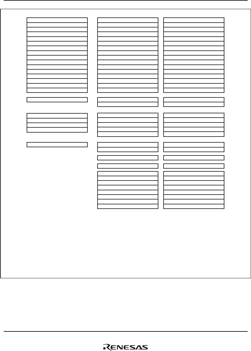
2. Programming Model
Rev.1.00 Jan. 10, 2008 Page 29 of 1658
REJ09B0261-0100
31 0
R0_BANK0*1,*2
R1_BANK0*2
R2_BANK0*2
R3_BANK0*2
R4_BANK0*2
R5_BANK0*2
R6_BANK0*2
R7_BANK0*2
R8
R9
R10
R11
R12
R13
R14
R15
SR
GBR
MACH
MACL
PR
PC
(a) Register configuration
in user mode
31 0
R0_BANK1*1,*3
R1_BANK1*3
R2_BANK1*3
R3_BANK1*3
R4_BANK1*3
R5_BANK1*3
R6_BANK1*3
R7_BANK1*3
R8
R9
R10
R11
R12
R13
R14
R15
R0_BANK0*1,*4
R1_BANK0*4
R2_BANK0*4
R3_BANK0*4
R4_BANK0*4
R5_BANK0*4
R6_BANK0*4
R7_BANK0*4
(b) Register configuration in
privileged mode (RB = 1)
GBR
MACH
MACL
VBR
PR
SR
SSR
PC
SPC
31 0
R0_BANK1*1,*3
R1_BANK1*3
R2_BANK1*3
R3_BANK1*3
R4_BANK1*3
R5_BANK1*3
R6_BANK1*3
R7_BANK1*3
R8
R9
R10
R11
R12
R13
R14
R15
R0_BANK0*1,*4
R1_BANK0*4
R2_BANK0*4
R3_BANK0*4
R4_BANK0*4
R5_BANK0*4
R6_BANK0*4
R7_BANK0*4
(c) Register configuration in
privileged mode (RB = 0)
GBR
MACH
MACL
VBR
PR
SR
SSR
PC
SPC
SGR
DBR
SGR
DBR
R0 is used as the index register in indexed register-indirect addressing mode and
indexed GBR indirect addressing mode.
Banked registers
Banked registers
Accessed as general registers when the RB bit is set to 1 in SR. Accessed only by
LDC/STC instructions when the RB bit is cleared to 0.
Banked registers
Accessed as general registers when the RB bit is cleared to 0 in SR. Accessed only
by LDC/STC instructions when the RB bit is set to 1.
Notes: 1.
2.
3.
4.
Figure 2.2 CPU Register Configuration in Each Processing Mode
2. Programming Model
Rev.1.00 Jan. 10, 2008 Page 30 of 1658
REJ09B0261-0100
2.2.2 General Registers
Figure 2.3 shows the relationship between the processing modes and general registers. This LSI
has twenty-four 32-bit general registers (R0_BANK0 to R7_BANK0, R0_BANK1 to
R7_BANK1, and R8 to R15). However, only 16 of these can be accessed as general registers R0
to R15 in one processing mode. This LSI has two processing modes, user mode and privileged
mode.
• R0_BANK0 to R7_BANK0
Allocated to R0 to R7 in user mode (SR.MD = 0)
Allocated to R0 to R7 when SR.RB = 0 in privileged mode (SR.MD = 1).
• R0_BANK1 to R7_BANK1
Cannot be accessed in user mode.
Allocated to R0 to R7 when SR.RB = 1 in privileged mode.
SR.MD = 0 or
(SR.MD = 1, SR.RB = 0)
R0_BANK0
R1_BANK0
R2_BANK0
R3_BANK0
R4_BANK0
R5_BANK0
R6_BANK0
R7_BANK0
R0_BANK0
R1_BANK0
R2_BANK0
R3_BANK0
R4_BANK0
R5_BANK0
R6_BANK0
R7_BANK0
R0_BANK1
R1_BANK1
R2_BANK1
R3_BANK1
R4_BANK1
R5_BANK1
R6_BANK1
R7_BANK1
R0_BANK1
R1_BANK1
R2_BANK1
R3_BANK1
R4_BANK1
R5_BANK1
R6_BANK1
R7_BANK1
R0
R1
R2
R3
R4
R5
R6
R7
R0
R1
R2
R3
R4
R5
R6
R7
R8
R9
R10
R11
R12
R13
R14
R15
R8
R9
R10
R11
R12
R13
R14
R15
R8
R9
R10
R11
R12
R13
R14
R15
(SR.MD = 1, SR.RB = 1)
Figure 2.3 General Registers

2. Programming Model
Rev.1.00 Jan. 10, 2008 Page 31 of 1658
REJ09B0261-0100
Note on Programming: As the user's R0 to R7 are assigned to R0_BANK0 to R7_BANK0, and
after an exception or interrupt R0 to R7 are assigned to R0_BANK1 to
R7_BANK1, it is not necessary for the interrupt handler to save and
restore the user's R0 to R7 (R0_BANK0 to R7_BANK0).
2.2.3 Floating-Point Registers
Figure 2.4 shows the floating-point register configuration. There are thirty-two 32-bit floating-
point registers, FPR0_BANK0 to FPR15_BANK0, AND FPR0_BANK1 to FPR15_BANK1,
comprising two banks. These registers are referenced as FR0 to FR15, DR0/2/4/6/8/10/12/14,
FV0/4/8/12, XF0 to XF15, XD0/2/4/6/8/10/12/14, or XMTRX. Reference names of each register
are defined depending on the state of the FR bit in FPSCR (see figure 2.4).
1. Floating-point registers, FPRn_BANKj (32 registers)
FPR0_BANK0 to FPR15_BANK0
FPR0_BANK1 to FPR15_BANK1
2. Single-precision floating-point registers, FRi (16 registers)
When FPSCR.FR = 0, FR0 to FR15 are assigned to FPR0_BANK0 to FPR15_BANK0;
when FPSCR.FR = 1, FR0 to FR15 are assigned to FPR0_BANK1 to FPR15_BANK1.
3. Double-precision floating-point registers or single-precision floating-point registers, DRi (8
registers): A DR register comprises two FR registers.
DR0 = {FR0, FR1}, DR2 = {FR2, FR3}, DR4 = {FR4, FR5}, DR6 = {FR6, FR7},
DR8 = {FR8, FR9}, DR10 = {FR10, FR11}, DR12 = {FR12, FR13}, DR14 = {FR14, FR15}
4. Single-precision floating-point vector registers, FVi (4 registers): An FV register comprises
four FR registers.
FV0 = {FR0, FR1, FR2, FR3}, FV4 = {FR4, FR5, FR6, FR7},
FV8 = {FR8, FR9, FR10, FR11}, FV12 = {FR12, FR13, FR14, FR15}
5. Single-precision floating-point extended registers, XFi (16 registers)
When FPSCR.FR = 0, XF0 to XF15 are assigned to FPR0_BANK1 to FPR15_BANK1;
when FPSCR.FR = 1, XF0 to XF15 are assigned to FPR0_BANK0 to FPR15_BANK0.
6. Double-precision floating-point extended registers, XDi (8 registers): An XD register
comprises two XF registers.
XD0 = {XF0, XF1}, XD2 = {XF2, XF3}, XD4 = {XF4, XF5}, XD6 = {XF6, XF7},
XD8 = {XF8, XF9}, XD10 = {XF10, XF11}, XD12 = {XF12, XF13}, XD14 = {XF14, XF15}
2. Programming Model
Rev.1.00 Jan. 10, 2008 Page 32 of 1658
REJ09B0261-0100
7. Single-precision floating-point extended register matrix, XMTRX: XMTRX comprises all 16
XF registers.
XMTRX = XF0 XF4 XF8 XF12
XF1 XF5 XF9 XF13
XF2 XF6 XF10 XF14
XF3 XF7 XF11 XF15
FPR0_BANK0
FPR1_BANK0
FPR2_BANK0
FPR3_BANK0
FPR4_BANK0
FPR5_BANK0
FPR6_BANK0
FPR7_BANK0
FPR8_BANK0
FPR9_BANK0
FPR10_BANK0
FPR11_BANK0
FPR12_BANK0
FPR13_BANK0
FPR14_BANK0
FPR15_BANK0
XF0
XF1
XF2
XF3
XF4
XF5
XF6
XF7
XF8
XF9
XF10
XF11
XF12
XF13
XF14
XF15
FR0
FR1
FR2
FR3
FR4
FR5
FR6
FR7
FR8
FR9
FR10
FR11
FR12
FR13
FR14
FR15
DR0
DR2
DR4
DR6
DR8
DR10
DR12
DR14
FV0
FV4
FV8
FV12
XD0 XMTRX
XD2
XD4
XD6
XD8
XD10
XD12
XD14
FPR0_BANK1
FPR1_BANK1
FPR2_BANK1
FPR3_BANK1
FPR4_BANK1
FPR5_BANK1
FPR6_BANK1
FPR7_BANK1
FPR8_BANK1
FPR9_BANK1
FPR10_BANK1
FPR11_BANK1
FPR12_BANK1
FPR13_BANK1
FPR14_BANK1
FPR15_BANK1
XF0
XF1
XF2
XF3
XF4
XF5
XF6
XF7
XF8
XF9
XF10
XF11
XF12
XF13
XF14
XF15
FR0
FR1
FR2
FR3
FR4
FR5
FR6
FR7
FR8
FR9
FR10
FR11
FR12
FR13
FR14
FR15
DR0
DR2
DR4
DR6
DR8
DR10
DR12
DR14
FV0
FV4
FV8
FV12
XD0XMTRX
XD2
XD4
XD6
XD8
XD10
XD12
XD14
FPSCR.FR = 0 FPSCR.FR = 1
Figure 2.4 Floating-Point Registers

2. Programming Model
Rev.1.00 Jan. 10, 2008 Page 33 of 1658
REJ09B0261-0100
2.2.4 Control Registers
(1) Status Register (SR)
31 30 29 28 27 26 25 24 23 22 21 20 19 18 17 16
BIt:
0111000000000000
MD RB BL
FD M Q IMASK S T
Initial value:
RR/WR/WR/WRRRRRRRRRRRR
R/W:
15 14 13 12 11 10 9 8 7 6 5 4 3 2 1 0
BIt:
0000000011110000
Initial value:
R/W R R R R R R/W R/W R/W R/W R/W R/W R R R/W R/W
R/W:
Bit Bit Name
Initial
Value R/W Description
31 — 0 R Reserved
For details on reading/writing this bit, see General
Precautions on Handling of Product.
30 MD 1 R/W Processing Mode
Selects the processing mode.
0: User mode (Some instructions cannot be executed
and some resources cannot be accessed.)
1: Privileged mode
This bit is set to 1 by an exception or interrupt.
29 RB 1 R/W Privileged Mode General Register Bank Specification
Bit
0: R0_BANK0 to R7_BANK0 are accessed as general
registers R0 to R7 and R0_BANK1 to R7_BANK1 can
be accessed using LDC/STC instructions
1: R0_BANK1 to R7_BANK1 are accessed as general
registers R0 to R7 and R0_BANK0–R7_BANK0 can
be accessed using LDC/STC instructions
This bit is set to 1 by an exception or interrupt.
28 BL 1 R/W Exception/Interrupt Block Bit
This bit is set to 1 by a reset, a general exception, or an
interrupt.
While this bit is set to 1, an interrupt request is masked.
In this case, this processor enters the reset state when
a general exception other than a user break occurs.

2. Programming Model
Rev.1.00 Jan. 10, 2008 Page 34 of 1658
REJ09B0261-0100
Bit Bit Name
Initial
Value R/W Description
27 to 16 — All 0 R Reserved
For details on reading/writing this bit, see General
Precautions on Handling of Product.
15 FD 0 R/W FPU Disable Bit
When this bit is set to 1 and an FPU instruction is not in
a delay slot, a general FPU disable exception occurs.
When this bit is set to 1 and an FPU instruction is in a
delay slot, a slot FPU disable exception occurs. (FPU
instructions: H'F*** instructions and LDS (.L)/STS(.L)
instructions using FPUL/FPSCR)
14 to 10 — All 0 R Reserved
For details on reading/writing this bit, see General
Precautions on Handling of Product.
9 M 0 R/W M Bit
Used by the DIV0S, DIV0U, and DIV1 instructions.
8 Q 0 R/W Q Bit
Used by the DIV0S, DIV0U, and DIV1 instructions.
7 to 4 IMASK 1111 R/W Interrupt Mask Level Bits
An interrupt whose priority is equal to or less than the
value of the IMASK bits is masked. It can be chosen by
CPU operation mode register (CPUOPM) whether the
level of IMASK is changed to accept an interrupt or not
when an interrupt is occurred. For details, see appendix
A, CPU Operation Mode Register (CPUOPM).
3, 2 — All 0 R Reserved
For details on reading/writing this bit, see General
Precautions on Handling of Product.
1 S 0 R/W S Bit
Used by the MAC instruction.
0 T 0 R/W T Bit
Indicates true/false condition, carry/borrow, or
overflow/underflow.
For details, see section 3, Instruction Set.

2. Programming Model
Rev.1.00 Jan. 10, 2008 Page 35 of 1658
REJ09B0261-0100
(2) Saved Status Register (SSR) (32 bits, Privileged Mode, Initial Value = Undefined)
The contents of SR are saved to SSR in the event of an exception or interrupt.
(3) Saved Program Counter (SPC) (32 bits, Privileged Mode, Initial Value = Undefined)
The address of an instruction at which an interrupt or exception occurs is saved to SPC.
(4) Global Base Register (GBR) (32 bits, Initial Value = Undefined)
GBR is referenced as the base address of addressing @(disp,GBR) and @(R0,GBR).
(5) Vector Base Register (VBR) (32 bits, Privileged Mode, Initial Value = H'00000000)
VBR is referenced as the branch destination base address in the event of an exception or interrupt.
For details, see section 5, Exception Handling.
(6) Saved General Register 15 (SGR) (32 bits, Privileged Mode, Initial Value = Undefined)
The contents of R15 are saved to SGR in the event of an exception or interrupt.
(7) Debug Base Register (DBR) (32 bits, Privileged Mode, Initial Value = Undefined)
When the user break debugging function is enabled (CBCR.UBDE = 1), DBR is referenced as the
branch destination address of the user break handler instead of VBR.
2.2.5 System Registers
(1) Multiply-and-Accumulate Registers (MACH and MACL) (32 bits, Initial Value =
Undefined)
MACH and MACL are used for the added value in a MAC instruction, and to store the operation
result of a MAC or MUL instruction.
(2) Procedure Register (PR) (32 bits, Initial Value = Undefined)
The return address is stored in PR in a subroutine call using a BSR, BSRF, or JSR instruction. PR
is referenced by the subroutine return instruction (RTS).
(3) Program Counter (PC) (32 bits, Initial Value = H'A0000000)
PC indicates the address of the instruction currently being executed.

2. Programming Model
Rev.1.00 Jan. 10, 2008 Page 36 of 1658
REJ09B0261-0100
(4) Floating-Point Status/Control Register (FPSCR)
31 30 29 28 27 26 25 24 23 22 21 20 19 18 17 16
0000000000000100
RRRRRRRRRRR/WR/WR/WR/WR/W
R/W
15 14 13 12 11 10 9 8 7 6 5 4 3 2 1 0
0000000000000001
R/W R/W R/W R/W R/W R/W R/W R/W R/W R/W R/W R/W R/W R/W R/W R/W
Enable (EN)
FR SZ PR DN
FlagRM
Cause
Cause
BIt:
Initial value:
R/W:
BIt:
Initial value:
R/W:
Bit Bit Name
Initial
Value R/W Description
31 to 22 — All 0 R Reserved
For details on reading/writing this bit, see General
Precautions on Handling of Product.
21 FR 0 R/W Floating-Point Register Bank
0: FPR0_BANK0 to FPR15_BANK0 are assigned to
FR0 to FR15 and FPR0_BANK1 to FPR15_BANK1
are assigned to XF0 to XF15
1: FPR0_BANK0 to FPR15_BANK0 are assigned to
XF0 to XF15 and FPR0_BANK1 to FPR15_BANK1
are assigned to FR0 to FR15
20 SZ 0 R/W Transfer Size Mode
0: Data size of FMOV instruction is 32-bits
1: Data size of FMOV instruction is a 32-bit register
pair (64 bits)
For relationship between the SZ bit, PR bit, and endian,
see figure 2.5.
19 PR 0 R/W Precision Mode
0: Floating-point instructions are executed as
single-precision operations
1: Floating-point instructions are executed as
double-precision operations (graphics support
instructions are undefined)
For relationship between the SZ bit, PR bit, and endian,
see figure 2.5
18 DN 1 R/W Denormalization Mode
0: Denormalized number is treated as such
1: Denormalized number is treated as zero

2. Programming Model
Rev.1.00 Jan. 10, 2008 Page 37 of 1658
REJ09B0261-0100
Bit Bit Name
Initial
Value R/W Description
17 to 12 Cause 000000 R/W
11 to 7 Enable (EN) 00000 R/W
6 to 2 Flag 00000 R/W
FPU Exception Cause Field
FPU Exception Enable Field
FPU Exception Flag Field
Each time an FPU operation instruction is executed, the
FPU exception cause field is cleared to 0. When an
FPU exception occurs, the bits corresponding to FPU
exception cause field and flag field are set to 1. The
FPU exception flag field remains set to 1 until it is
cleared to 0 by software.
For bit allocations of each field, see table 2.2.
1, 0 RM 01 R/W Rounding Mode
These bits select the rounding mode.
00: Round to Nearest
01: Round to Zero
10: Reserved
11: Reserved
2. Programming Model
Rev.1.00 Jan. 10, 2008 Page 38 of 1658
REJ09B0261-0100
<Big endian>
DR (2i)
FR (2i) FR (2i+1)
8n+4 8n+78n 8n+3
63 0
63 32 31 0
Floating-point register
Memory area
63 0
<Little endian>
Floating-point register
Memory area
DR (2i)
FR (2i) FR (2i+1)
4n 4m4n+3 4m+3
63 0
63 32 31 0
DR (2i)
FR (2i+1)FR (2i)
8n+48n+78n+3 8n
63 0
63 32 31 0
(1) SZ = 0 (2) SZ = 1, PR = 0
63 0 63 0
DR (2i)
FR (2i+1)FR (2i)
8n8n+38n+7 8n+4
63 0
63 32 31 0
(3) SZ = 1, PR = 1
63 0
*
1,
*
2
*
2
Notes: 1. In the case of SZ = 0 and PR = 0, DR register can not be used.
2. The bit-location of DR register is used for double precision format when PR = 1.
(In the case of (2), it is used when PR is changed from 0 to 1.)
Figure 2.5 Relationship between SZ bit and Endian
Table 2.2 Bit Allocation for FPU Exception Handling
Field Name
FPU
Error (E)
Invalid
Operation (V)
Division
by Zero (Z)
Overflow
(O)
Underflow
(U)
Inexact
(I)
Cause FPU exception
cause field
Bit 17 Bit 16 Bit 15 Bit 14 Bit 13 Bit 12
Enable FPU exception
enable field
None Bit 11 Bit 10 Bit 9 Bit 8 Bit 7
Flag FPU exception flag
field
None Bit 6 Bit 5 Bit 4 Bit 3 Bit 2
(5) Floating-Point Communication Register (FPUL) (32 bits, Initial Value = Undefined)
Information is transferred between the FPU and CPU via FPUL.

2. Programming Model
Rev.1.00 Jan. 10, 2008 Page 39 of 1658
REJ09B0261-0100
2.3 Memory-Mapped Registers
Some control registers are mapped to the following memory areas. Each of the mapped registers
has two addresses.
H'1C00 0000 to H'1FFF FFFF
H'FC00 0000 to H'FFFF FFFF
These two areas are used as follows.
• H'1C00 0000 to H'1FFF FFFF
This area must be accessed using the address translation function of the MMU.
Setting the page number of this area to the corresponding field of the TLB enables access to a
memory-mapped register.
The operation of an access to this area without using the address translation function of the
MMU is not guaranteed.
• H'FC00 0000 to H'FFFF FFFF
Access to area H'FC00 0000 to H'FFFF FFFF in user mode will cause an address error.
Memory-mapped registers can be referenced in user mode by means of access that involves
address translation.
Note: Do not access addresses to which registers are not mapped in either area. The operation of
an access to an address with no register mapped is undefined. Also, memory-mapped
registers must be accessed using a fixed data size. The operation of an access using an
invalid data size is undefined.
2. Programming Model
Rev.1.00 Jan. 10, 2008 Page 40 of 1658
REJ09B0261-0100
2.4 Data Formats in Registers
Register operands are always longwords (32 bits). When a memory operand is only a byte (8 bits)
or a word (16 bits), it is sign-extended into a longword when loaded into a register.
31
SS
S
067
67 0
31
SS
S
01415
1415 0
Figure 2.6 Formats of Byte Data and Word Data in Register
2.5 Data Formats in Memory
Memory data formats are classified into bytes, words, and longwords. Memory can be accessed in
an 8-bit byte, 16-bit word, or 32-bit longword form. A memory operand less than 32 bits in length
is sign-extended before being loaded into a register.
A word operand must be accessed starting from a word boundary (even address of a 2-byte unit:
address 2n), and a longword operand starting from a longword boundary (even address of a 4-byte
unit: address 4n). An address error will result if this rule is not observed. A byte operand can be
accessed from any address.
Big endian or little endian byte order can be selected for the data format. The endian should be set
with the external pin after a power-on reset. The endian cannot be changed dynamically. Bit
positions are numbered left to right from most-significant to least-significant. Thus, in a 32-bit
longword, the leftmost bit, bit 31, is the most significant bit and the rightmost bit, bit 0, is the least
significant bit.
The data format in memory is shown in figure 2.7.

2. Programming Model
Rev.1.00 Jan. 10, 2008 Page 41 of 1658
REJ09B0261-0100
Address A
A
70707070
31
15 0 15 0
31 0
15 0
31 0
23 15 7 0
A + 1 A + 2 A + 3
Byte 0
Word 0
Longword
Word 1
Byte 1 Byte 2 Byte 3
A + 11
70707070
31
15 0
23 15 7 0
A + 10 A + 9 A + 8
Byte 3
Word 1
Longword
Word 0
Byte 2 Byte 1 Byte 0
Address A + 4
Address A + 8
Address A + 8
Address A + 4
Address A
Big endian Little endian
Figure 2.7 Data Formats in Memory
For the 64-bit data format, see figure 2.5.
2.6 Processing States
This LSI has major three processing states: the reset state, instruction execution state, and power-
down state.
(1) Reset State
In this state the CPU is reset. The reset state is divided into the power-on reset state and the
manual reset.
In the power-on reset state, the internal state of the CPU and the on-chip peripheral module
registers are initialized. In the manual reset state, the internal state of the CPU and some registers
of on-chip peripheral modules are initialized. For details, see register descriptions for each section.
(2) Instruction Execution State
In this state, the CPU executes program instructions in sequence. The Instruction execution state
has the normal program execution state and the exception handling state.
(3) Power-Down State
In a power-down state, CPU halts operation and power consumption is reduced. The power-down
state is entered by executing a SLEEP instruction. There are two modes in the power-down state:
sleep mode and standby mode. For details, see section 17, Power-Down mode.

2. Programming Model
Rev.1.00 Jan. 10, 2008 Page 42 of 1658
REJ09B0261-0100
From any state
when reset/manual
reset input
Reset state
Instruction execution state Sleep instruction execution
Power-down state
Interrupt occurence
Reset/manual
reset clearance
Reset/manual
reset input
Reset/manual
reset input
Figure 2.8 Processing State Transitions

2. Programming Model
Rev.1.00 Jan. 10, 2008 Page 43 of 1658
REJ09B0261-0100
2.7 Usage Notes
2.7.1 Notes on Self-Modifying Code
To accelerate the processing speed, the instruction prefetching capability of this LSI has been
significantly enhanced from that of the SH-4. Therefore, in the case when a code in memory is
rewritten and attempted to be executed immediately, there is increased possibility that the code
before being modified, which has already been prefetched, is executed.
To ensure execution of the modified code, one of the following sequence of instructions should be
executed between the code rewriting instruction and execution of the modified code.
(1) When the Codes to be Modified are in Non-Cacheable Area
SYNCO
ICBI @Rn
The target for the ICBI instruction can be any address within the range where no address error
exception occurs.
(2) When the Codes to be Modified are in Cacheable Area (Write-Through)
SYNCO
ICBI @Rn
All instruction cache areas corresponding to the modified codes should be invalidated by the ICBI
instruction. The ICBI instruction should be issued to each cache line. One cache line is 32 bytes.
(3) When the Codes to be Modified are in Cacheable Area (Copy-Back)
OCBP @Rm or OCBWB @Rm
SYNCO
ICBI @Rn
All operand cache areas corresponding to the modified codes should be written back to the main
memory by the OCBP or OCBWB instruction. Then all instruction cache areas corresponding to
the modified codes should be invalidated by the ICBI instruction. The OCBP, OCBWB, and ICBI
instruction should be issued to each cache line. One cache line is 32 bytes.
Note: Self-modifying code is the processing which executes instructions while dynamically
rewriting the codes in memory.

2. Programming Model
Rev.1.00 Jan. 10, 2008 Page 44 of 1658
REJ09B0261-0100

3. Instruction Set
Rev.1.00 Jan. 10, 2008 Page 45 of 1658
REJ09B0261-0100
Section 3 Instruction Set
This LSI's instruction set is implemented with 16-bit fixed-length instructions. This LSI can use
byte (8-bit), word (16-bit), longword (32-bit), and quadword (64-bit) data sizes for memory
access. Single-precision floating-point data (32 bits) can be moved to and from memory using
longword or quadword size. Double-precision floating-point data (64 bits) can be moved to and
from memory using longword size. When this LSI moves byte-size or word-size data from
memory to a register, the data is sign-extended.
3.1 Execution Environment
(1) PC
At the start of instruction execution, the PC indicates the address of the instruction itself.
(2) Load-Store Architecture
This LSI has a load-store architecture in which operations are basically executed using registers.
Except for bit-manipulation operations such as logical AND that are executed directly in memory,
operands in an operation that requires memory access are loaded into registers and the operation is
executed between the registers.
(3) Delayed Branches
Except for the two branch instructions BF and BT, this LSI's branch instructions and RTE are
delayed branches. In a delayed branch, the instruction following the branch is executed before the
branch destination instruction.
(4) Delay Slot
This execution slot following a delayed branch is called a delay slot. For example, the BRA
execution sequence is as follows:

3. Instruction Set
Rev.1.00 Jan. 10, 2008 Page 46 of 1658
REJ09B0261-0100
Table 3.1 Execution Order of Delayed Branch Instructions
Instructions Execution Order
BRA TARGET (Delayed branch instruction) BRA
ADD (Delay slot) ↓
: ADD
: ↓
TARGET target-inst (Branch destination instruction) target-inst
A slot illegal instruction exception may occur when a specific instruction is executed in a delay
slot. For details, see section 5, Exception Handling. The instruction following BF/S or BT/S for
which the branch is not taken is also a delay slot instruction.
(5) T Bit
The T bit in SR is used to show the result of a compare operation, and is referenced by a
conditional branch instruction. An example of the use of a conditional branch instruction is shown
below.
ADD #1, R0 ; T bit is not changed by ADD operation
CMP/EQ R1, R0 ; If R0 = R1, T bit is set to 1
BT TARGET ; Branches to TARGET if T bit = 1 (R0 = R1)
In an RTE delay slot, the SR bits are referenced as follows. In instruction access, the MD bit is
used before modification, and in data access, the MD bit is accessed after modification. The other
bits—S, T, M, Q, FD, BL, and RB—after modification are used for delay slot instruction
execution. The STC and STC.L SR instructions access all SR bits after modification.
(6) Constant Values
An 8-bit constant value can be specified by the instruction code and an immediate value. 16-bit
and 32-bit constant values can be defined as literal constant values in memory, and can be
referenced by a PC-relative load instruction.
MOV.W @(disp, PC), Rn
MOV.L @(disp, PC), Rn
There are no PC-relative load instructions for floating-point operations. However, it is possible to
set 0.0 or 1.0 by using the FLDI0 or FLDI1 instruction on a single-precision floating-point
register.
3. Instruction Set
Rev.1.00 Jan. 10, 2008 Page 47 of 1658
REJ09B0261-0100
3.2 Addressing Modes
Addressing modes and effective address calculation methods are shown in table 3.2. When a
location in virtual memory space is accessed (AT in MMUCR = 1), the effective address is
translated into a physical memory address. If multiple virtual memory space systems are selected
(SV in MMUCR = 0), the least significant bit of PTEH is also referenced as the access ASID. For
details, see section 7, Memory Management Unit (MMU).
Table 3.2 Addressing Modes and Effective Addresses
Addressing
Mode
Instruction
Format Effective Address Calculation Method
Calculation
Formula
Register
direct
Rn Effective address is register Rn.
(Operand is register Rn contents.)
—
Register
indirect
@Rn Effective address is register Rn contents.
Rn Rn
Rn → EA
(EA: effective
address)
Register
indirect
with post-
increment
@Rn+ Effective address is register Rn contents.
A constant is added to Rn after instruction
execution: 1 for a byte operand, 2 for a word
operand, 4 for a longword operand, 8 for a
quadword operand.
Rn Rn
1/2/4
+
Rn + 1/2/4
Rn → EA
After instruction
execution
Byte:
Rn + 1 → Rn
Word:
Rn + 2 → Rn
Longword:
Rn + 4 → Rn
Quadword:
Rn + 8 → Rn
3. Instruction Set
Rev.1.00 Jan. 10, 2008 Page 48 of 1658
REJ09B0261-0100
Addressing
Mode
Instruction
Format Effective Address Calculation Method
Calculation
Formula
Register
indirect
with pre-
decrement
@–Rn Effective address is register Rn contents,
decremented by a constant beforehand:
1 for a byte operand, 2 for a word operand,
4 for a longword operand, 8 for a quadword
operand.
Rn
1/2/4
Rn – 1/2/4/8
–
Rn – 1/2/4
Byte:
Rn – 1 → Rn
Word:
Rn – 2 → Rn
Longword:
Rn – 4 → Rn
Quadword:
Rn – 8 → Rn
Rn → EA
(Instruction
executed
with Rn after
calculation)
Register
indirect with
displacement
@(disp:4, Rn) Effective address is register Rn contents with
4-bit displacement disp added. After disp is
zero-extended, it is multiplied by 1 (byte), 2
(word), or 4 (longword), according to the operand
size.
Rn
Rn + disp × 1/2/4
+
×
1/2/4
disp
(zero-extended)
Byte: Rn + disp
→ EA
Word: Rn + disp
× 2 → EA
Longword:
Rn + disp × 4 →
EA
Indexed
register
indirect
@(R0, Rn) Effective address is sum of register Rn and R0
contents.
Rn
R0
Rn + R0
+
Rn + R0 → EA
3. Instruction Set
Rev.1.00 Jan. 10, 2008 Page 49 of 1658
REJ09B0261-0100
Addressing
Mode
Instruction
Format Effective Address Calculation Method
Calculation
Formula
GBR indirect
with displace-
ment
@(disp:8,
GBR)
Effective address is register GBR contents with
8-bit displacement disp added. After disp is
zero-extended, it is multiplied by 1 (byte), 2 (word),
or 4 (longword), according to the operand size.
GBR
1/2/4
GBR
+ disp × 1/2/4
+
×
disp
(zero-extended)
Byte: GBR +
disp → EA
Word: GBR +
disp × 2 → EA
Longword:
GBR + disp ×
4 → EA
Indexed GBR
indirect
@(R0, GBR) Effective address is sum of register GBR and R0
contents.
GBR
R0
GBR + R0
+
GBR + R0 →
EA
PC-relative
with
displacement
@(disp:8, PC) Effective address is PC + 4 with 8-bit displacement
disp added. After disp is zero-extended, it is
multiplied by 2 (word), or 4 (longword), according
to the operand size. With a longword operand,
the lower 2 bits of PC are masked.
PC
H'FFFF FFFC
PC + 4 + disp
× 2
or PC &
H'FFFF FFFC
+ 4 + disp × 4
+
4
2/4
×
+
&*
disp
(zero-extended)
* With longword operand
Word: PC + 4
+ disp × 2 →
EA
Longword:
PC & H'FFFF
FFFC + 4 +
disp × 4 → EA
3. Instruction Set
Rev.1.00 Jan. 10, 2008 Page 50 of 1658
REJ09B0261-0100
Addressing
Mode
Instruction
Format Effective Address Calculation Method
Calculation
Formula
PC-relative disp:8 Effective address is PC + 4 with 8-bit displacement
disp added after being sign-extended and
multiplied by 2.
2
+
×
disp
(sign-extended)
4
+
PC
PC + 4 + disp × 2
PC + 4 + disp
× 2 → Branch-
Target
PC-relative disp:12 Effective address is PC + 4 with 12-bit displacement
disp added after being sign-extended and
multiplied by 2.
2
+
×
disp
(sign-extended)
4
+
PC
PC + 4 + disp × 2
PC + 4 + disp
× 2 → Branch-
Target
Rn Effective address is sum of PC + 4 and Rn.
PC
4
Rn
+
+PC + 4 + Rn
PC + 4 + Rn →
Branch-Target

3. Instruction Set
Rev.1.00 Jan. 10, 2008 Page 51 of 1658
REJ09B0261-0100
Addressing
Mode
Instruction
Format Effective Address Calculation Method
Calculation
Formula
Immediate #imm:8 8-bit immediate data imm of TST, AND, OR, or XOR
instruction is zero-extended.
—
#imm:8 8-bit immediate data imm of MOV, ADD, or CMP/EQ
instruction is sign-extended.
—
#imm:8 8-bit immediate data imm of TRAPA instruction is
zero-extended and multiplied by 4.
—
Note: For the addressing modes below that use a displacement (disp), the assembler descriptions
in this manual show the value before scaling (×1, ×2, or ×4) is performed according to the
operand size. This is done to clarify the operation of the LSI. Refer to the relevant
assembler notation rules for the actual assembler descriptions.
@ (disp:4, Rn) ; Register indirect with displacement
@ (disp:8, GBR) ; GBR indirect with displacement
@ (disp:8, PC) ; PC-relative with displacement
disp:8, disp:12 ; PC-relative

3. Instruction Set
Rev.1.00 Jan. 10, 2008 Page 52 of 1658
REJ09B0261-0100
3.3 Instruction Set
Table 3.3 shows the notation used in the SH instruction lists shown in tables 3.4 to 3.13.
Table 3.3 Notation Used in Instruction List
Item Format Description
Instruction
mnemonic
OP.Sz SRC, DEST OP: Operation code
Sz: Size
SRC: Source operand
DEST: Source and/or destination operand
Rm: Source register
Rn: Destination register
imm: Immediate data
disp: Displacement
Operation
notation
→, ← Transfer direction
(xx) Memory operand
M/Q/T SR flag bits
& Logical AND of individual bits
| Logical OR of individual bits
∧ Logical exclusive-OR of individual bits
~ Logical NOT of individual bits
<<n, >>n n-bit shift
Instruction code MSB ↔ LSB mmmm: Register number (Rm, FRm)
nnnn: Register number (Rn, FRn)
0000: R0, FR0
0001: R1, FR1
:
1111: R15, FR15
mmm: Register number (DRm, XDm, Rm_BANK)
nnn: Register number (DRn, XDn, Rn_BANK)
000: DR0, XD0, R0_BANK
001: DR2, XD2, R1_BANK
:
111: DR14, XD14, R7_BANK
mm: Register number (FVm)
nn: Register number (FVn)
00: FV0
01: FV4
10: FV8
11: FV12
iiii: Immediate data
dddd: Displacement

3. Instruction Set
Rev.1.00 Jan. 10, 2008 Page 53 of 1658
REJ09B0261-0100
Item Format Description
Privileged mode "Privileged" means the instruction can only be executed
in privileged mode.
T bit Value of T bit after
instruction execution
—: No change
New ⎯ "New" means the instruction which has been newly
added in the SH-4A with H’20-valued VER bits in the
processor version register (PVR).
Note: Scaling (×1, ×2, ×4, or ×8) is executed according to the size of the instruction operand.
Table 3.4 Fixed-Point Transfer Instructions
Instruction Operation Instruction Code Privileged T Bit New
MOV #imm,Rn imm → sign extension → Rn 1110nnnniiiiiiii — — —
MOV.W @(disp*,PC), Rn (disp × 2 + PC + 4) → sign
extension → Rn
1001nnnndddddddd — — —
MOV.L @(disp*,PC), Rn (disp × 4 + PC & H'FFFF FFFC
+ 4) → Rn
1101nnnndddddddd — — —
MOV Rm,Rn Rm → Rn 0110nnnnmmmm0011 — — —
MOV.B Rm,@Rn Rm → (Rn) 0010nnnnmmmm0000 — — —
MOV.W Rm,@Rn Rm → (Rn) 0010nnnnmmmm0001 — — —
MOV.L Rm,@Rn Rm → (Rn) 0010nnnnmmmm0010 — — —
MOV.B @Rm,Rn (Rm) → sign extension → Rn 0110nnnnmmmm0000 — — —
MOV.W @Rm,Rn (Rm) → sign extension → Rn 0110nnnnmmmm0001 — — —
MOV.L @Rm,Rn (Rm) → Rn 0110nnnnmmmm0010 — — —
MOV.B Rm,@-Rn Rn-1 → Rn, Rm → (Rn) 0010nnnnmmmm0100 — — —
MOV.W Rm,@-Rn Rn-2 → Rn, Rm → (Rn) 0010nnnnmmmm0101 — — —
MOV.L Rm,@-Rn Rn-4 → Rn, Rm → (Rn) 0010nnnnmmmm0110 — — —
MOV.B @Rm+,Rn (Rm)→ sign extension → Rn,
Rm + 1 → Rm
0110nnnnmmmm0100 — — —
MOV.W @Rm+,Rn (Rm) → sign extension → Rn,
Rm + 2 → Rm
0110nnnnmmmm0101 — — —
MOV.L @Rm+,Rn (Rm) → Rn, Rm + 4 → Rm 0110nnnnmmmm0110 — — —
MOV.B R0,@(disp*,Rn) R0 → (disp + Rn) 10000000nnnndddd — — —
MOV.W R0,@(disp*,Rn) R0 → (disp × 2 + Rn) 10000001nnnndddd — — —
MOV.L Rm,@(disp*,Rn) Rm → (disp × 4 + Rn) 0001nnnnmmmmdddd — — —

3. Instruction Set
Rev.1.00 Jan. 10, 2008 Page 54 of 1658
REJ09B0261-0100
Instruction Operation Instruction Code Privileged T Bit New
MOV.B @(disp*,Rm),R0 (disp + Rm) → sign
extension → R0
10000100mmmmdddd — — —
MOV.W @(disp*,Rm),R0 (disp × 2 + Rm) → sign
extension → R0
10000101mmmmdddd — — —
MOV.L @(disp*,Rm),Rn (disp × 4 + Rm) → Rn 0101nnnnmmmmdddd — — —
MOV.B Rm,@(R0,Rn) Rm → (R0 + Rn) 0000nnnnmmmm0100 — — —
MOV.W Rm,@(R0,Rn) Rm → (R0 + Rn) 0000nnnnmmmm0101 — — —
MOV.L Rm,@(R0,Rn) Rm → (R0 + Rn) 0000nnnnmmmm0110 — — —
MOV.B @(R0,Rm),Rn (R0 + Rm) →
sign extension → Rn
0000nnnnmmmm1100 — — —
MOV.W @(R0,Rm),Rn (R0 + Rm) →
sign extension → Rn
0000nnnnmmmm1101 — — —
MOV.L @(R0,Rm),Rn (R0 + Rm) → Rn 0000nnnnmmmm1110 — — —
MOV.B R0,@(disp*,GBR) R0 → (disp + GBR) 11000000dddddddd — — —
MOV.W R0,@(disp*,GBR) R0 → (disp × 2 + GBR) 11000001dddddddd — — —
MOV.L R0,@(disp*,GBR) R0 → (disp × 4 + GBR) 11000010dddddddd — — —
MOV.B @(disp*,GBR),R0 (disp + GBR) →
sign extension → R0
11000100dddddddd — — —
MOV.W @(disp*,GBR),R0 (disp × 2 + GBR) →
sign extension → R0
11000101dddddddd — — —
MOV.L @(disp*,GBR),R0 (disp × 4 + GBR) → R0 11000110dddddddd — — —
MOVA @(disp*,PC),R0 disp × 4 +
PC & H'FFFF FFFC
+ 4 → R0
11000111dddddddd — — —
MOVCO.L R0,@Rn LDST → T
If (T == 1) R0 → (Rn)
0 → LDST
0000nnnn01110011 ⎯ LDST New
MOVLI.L @Rm,R0 1 → LDST
(Rm) → R0
When interrupt/exception
occurred 0 → LDST
0000mmmm01100011 ⎯ ⎯ New
MOVUA.L @Rm,R0 (Rm) → R0
Load non-boundary
alignment data
0100mmmm10101001 ⎯ ⎯ New
MOVUA.L @Rm+,R0 (Rm) → R0, Rm + 4 →
Rm
Load non-boundary
alignment data
0100mmmm11101001 ⎯ ⎯ New

3. Instruction Set
Rev.1.00 Jan. 10, 2008 Page 55 of 1658
REJ09B0261-0100
Instruction Operation Instruction Code Privileged T Bit New
MOVT Rn T → Rn 0000nnnn00101001 — — —
SWAP.B Rm,Rn Rm → swap lower 2 bytes
→ Rn
0110nnnnmmmm1000 — — —
SWAP.W Rm,Rn Rm → swap upper/lower
words → Rn
0110nnnnmmmm1001 — — —
XTRCT Rm,Rn Rm:Rn middle 32 bits → Rn 0010nnnnmmmm1101 — — —
Note: * The assembler of Renesas uses the value after scaling (×1, ×2, or ×4) as the
displacement (disp).
Table 3.5 Arithmetic Operation Instructions
Instruction Operation Instruction Code Privileged T Bit New
ADD Rm,Rn Rn + Rm → Rn 0011nnnnmmmm1100 — — —
ADD #imm,Rn Rn + imm → Rn 0111nnnniiiiiiii — — —
ADDC Rm,Rn Rn + Rm + T → Rn,
carry → T
0011nnnnmmmm1110 — Carry —
ADDV Rm,Rn Rn + Rm → Rn,
overflow → T
0011nnnnmmmm1111 — Overflow —
CMP/EQ #imm,R0 When R0 = imm, 1 → T
Otherwise, 0 → T
10001000iiiiiiii — Comparison
result
—
CMP/EQ Rm,Rn When Rn = Rm, 1 → T
Otherwise, 0 → T
0011nnnnmmmm0000 — Comparison
result
—
CMP/HS Rm,Rn When Rn ≥ Rm (unsigned),
1 → T
Otherwise, 0 → T
0011nnnnmmmm0010 — Comparison
result
—
CMP/GE Rm,Rn When Rn ≥ Rm (signed),
1 → T
Otherwise, 0 → T
0011nnnnmmmm0011 — Comparison
result
—
CMP/HI Rm,Rn When Rn > Rm (unsigned),
1 → T
Otherwise, 0 → T
0011nnnnmmmm0110 — Comparison
result
—
CMP/GT Rm,Rn When Rn > Rm (signed),
1 → T
Otherwise, 0 → T
0011nnnnmmmm0111 — Comparison
result
—
CMP/PZ Rn When Rn ≥ 0, 1 → T
Otherwise, 0 → T
0100nnnn00010001 — Comparison
result
—
CMP/PL Rn When Rn > 0, 1 → T
Otherwise, 0 → T
0100nnnn00010101 — Comparison
result
—

3. Instruction Set
Rev.1.00 Jan. 10, 2008 Page 56 of 1658
REJ09B0261-0100
Instruction Operation Instruction Code Privileged T Bit New
CMP/STR Rm,Rn When any bytes are equal,
1 → T
Otherwise, 0 → T
0010nnnnmmmm1100 — Comparison
result
—
DIV1 Rm,Rn 1-step division (Rn ÷ Rm) 0011nnnnmmmm0100 — Calculation
result
—
DIV0S Rm,Rn MSB of Rn → Q,
MSB of Rm → M, M^Q →
T
0010nnnnmmmm0111 — Calculation
result
—
DIV0U 0 → M/Q/T 0000000000011001 — 0 —
DMULS.L Rm,Rn Signed,
Rn × Rm → MAC,
32 × 32 → 64 bits
0011nnnnmmmm1101 — — —
DMULU.L Rm,Rn Unsigned,
Rn × Rm → MAC,
32 × 32 → 64 bits
0011nnnnmmmm0101 — — —
DT Rn Rn – 1 → Rn;
when Rn = 0, 1 → T
When Rn ≠ 0, 0 → T
0100nnnn00010000 — Comparison
result
—
EXTS.B Rm,Rn Rm sign-extended from
byte → Rn
0110nnnnmmmm1110 — — —
EXTS.W Rm,Rn Rm sign-extended from
word → Rn
0110nnnnmmmm1111 — — —
EXTU.B Rm,Rn Rm zero-extended from
byte → Rn
0110nnnnmmmm1100 — — —
EXTU.W Rm,Rn Rm zero-extended from
word → Rn
0110nnnnmmmm1101 — — —
MAC.L @Rm+,@Rn+ Signed,
(Rn) × (Rm) + MAC →
MAC
Rn + 4 → Rn, Rm + 4 →
Rm
32 × 32 + 64 → 64 bits
0000nnnnmmmm1111 — — —
MAC.W @Rm+,@Rn+ Signed,
(Rn) × (Rm) + MAC →
MAC
Rn + 2 → Rn,
Rm + 2 → Rm
16 × 16 + 64 → 64 bits
0100nnnnmmmm1111 — — —
MUL.L Rm,Rn Rn × Rm → MACL
32 × 32 → 32 bits
0000nnnnmmmm0111 — — —
MULS.W Rm,Rn Signed,
Rn × Rm → MACL
16 × 16 → 32 bits
0010nnnnmmmm1111 — — —

3. Instruction Set
Rev.1.00 Jan. 10, 2008 Page 57 of 1658
REJ09B0261-0100
Instruction Operation Instruction Code Privileged T Bit New
MULU.W Rm,Rn Unsigned,
Rn × Rm → MACL
16 × 16 → 32 bits
0010nnnnmmmm1110 — — —
NEG Rm,Rn 0 – Rm → Rn 0110nnnnmmmm1011 — — —
NEGC Rm,Rn 0 – Rm – T → Rn,
borrow → T
0110nnnnmmmm1010 — Borrow —
SUB Rm,Rn Rn – Rm → Rn 0011nnnnmmmm1000 — — —
SUBC Rm,Rn Rn – Rm – T → Rn,
borrow → T
0011nnnnmmmm1010 — Borrow —
SUBV Rm,Rn Rn – Rm → Rn,
underflow → T
0011nnnnmmmm1011 — Underflow —
Table 3.6 Logic Operation Instructions
Instruction Operation Instruction Code Privileged T Bit New
AND Rm,Rn Rn & Rm → Rn 0010nnnnmmmm1001 — — —
AND #imm,R0 R0 & imm → R0 11001001iiiiiiii — — —
AND.B #imm, @(R0,GBR) (R0 + GBR) & imm
→ (R0 + GBR)
11001101iiiiiiii — — —
NOT Rm,Rn ~Rm → Rn 0110nnnnmmmm0111 — — —
OR Rm,Rn Rn | Rm → Rn 0010nnnnmmmm1011 — — —
OR #imm,R0 R0 | imm → R0 11001011iiiiiiii — — —
OR.B #imm, @(R0,GBR) (R0 + GBR) | imm
→ (R0 + GBR)
11001111iiiiiiii — — —
TAS.B @Rn When (Rn) = 0, 1 → T
Otherwise, 0 → T
In both cases,
1 → MSB of (Rn)
0100nnnn00011011 — Test
result
—
TST Rm,Rn Rn & Rm;
when result = 0, 1 → T
Otherwise, 0 → T
0010nnnnmmmm1000 — Test
result
—
TST #imm,R0 R0 & imm;
when result = 0, 1 → T
Otherwise, 0 → T
11001000iiiiiiii — Test
result
—
TST.B #imm, @(R0,GBR) (R0 + GBR) & imm;
when result = 0, 1 → T
Otherwise, 0 → T
11001100iiiiiiii — Test
result
—
XOR Rm,Rn Rn ∧ Rm → Rn 0010nnnnmmmm1010 — — —

3. Instruction Set
Rev.1.00 Jan. 10, 2008 Page 58 of 1658
REJ09B0261-0100
Instruction Operation Instruction Code Privileged T Bit New
XOR #imm,R0 R0 ∧ imm → R0 11001010iiiiiiii — — —
XOR.B #imm, @(R0,GBR) (R0 + GBR) ∧ imm →
(R0 + GBR)
11001110iiiiiiii — — —
Table 3.7 Shift Instructions
Instruction Operation Instruction Code Privileged T Bit New
ROTL Rn T ← Rn ← MSB 0100nnnn00000100 — MSB —
ROTR Rn LSB → Rn → T 0100nnnn00000101 — LSB —
ROTCL Rn T ← Rn ← T 0100nnnn00100100 — MSB —
ROTCR Rn T → Rn → T 0100nnnn00100101 — LSB —
SHAD Rm,Rn When Rm ≥ 0, Rn << Rm → Rn
When Rm < 0, Rn >> Rm →
[MSB → Rn]
0100nnnnmmmm1100 — — —
SHAL Rn T ← Rn ← 0 0100nnnn00100000 — MSB —
SHAR Rn MSB → Rn → T 0100nnnn00100001 — LSB —
SHLD Rm,Rn When Rm ≥ 0, Rn << Rm → Rn
When Rm < 0, Rn >> Rm →
[0 → Rn]
0100nnnnmmmm1101 — — —
SHLL Rn T ← Rn ← 0 0100nnnn00000000 — MSB —
SHLR Rn 0 → Rn → T 0100nnnn00000001 — LSB —
SHLL2 Rn Rn << 2 → Rn 0100nnnn00001000 — — —
SHLR2 Rn Rn >> 2 → Rn 0100nnnn00001001 — — —
SHLL8 Rn Rn << 8 → Rn 0100nnnn00011000 — — —
SHLR8 Rn Rn >> 8 → Rn 0100nnnn00011001 — — —
SHLL16 Rn Rn << 16 → Rn 0100nnnn00101000 — — —
SHLR16 Rn Rn >> 16 → Rn 0100nnnn00101001 — — —

3. Instruction Set
Rev.1.00 Jan. 10, 2008 Page 59 of 1658
REJ09B0261-0100
Table 3.8 Branch Instructions
Instruction Operation Instruction Code Privileged T Bit New
BF label When T = 0, disp × 2 + PC +
4 → PC
When T = 1, nop
10001011dddddddd — — —
BF/S label Delayed branch; when T = 0,
disp × 2 + PC + 4 → PC
When T = 1, nop
10001111dddddddd — — —
BT label When T = 1, disp × 2 + PC +
4 → PC
When T = 0, nop
10001001dddddddd — — —
BT/S label Delayed branch; when T = 1,
disp × 2 + PC + 4 → PC
When T = 0, nop
10001101dddddddd — — —
BRA label Delayed branch, disp × 2 +
PC + 4 → PC
1010dddddddddddd — — —
BRAF Rn Delayed branch, Rn + PC + 4 →
PC
0000nnnn00100011 — — —
BSR label Delayed branch, PC + 4 → PR,
disp × 2 + PC + 4 → PC
1011dddddddddddd — — —
BSRF Rn Delayed branch, PC + 4 → PR,
Rn + PC + 4 → PC
0000nnnn00000011 — — —
JMP @Rn Delayed branch, Rn → PC 0100nnnn00101011 — — —
JSR @Rn Delayed branch, PC + 4 → PR,
Rn → PC
0100nnnn00001011 — — —
RTS Delayed branch, PR → PC 0000000000001011 — — —
Table 3.9 System Control Instructions
Instruction Operation Instruction Code Privileged T Bit New
CLRMAC 0 → MACH, MACL 0000000000101000 — — —
CLRS 0 → S 0000000001001000 — — —
CLRT 0 → T 0000000000001000 — 0 —
ICBI @Rn Invalidates instruction cache block 0000nnnn11100011 ⎯ ⎯ New
LDC Rm,SR Rm → SR 0100mmmm00001110 Privileged LSB —
LDC Rm,GBR Rm → GBR 0100mmmm00011110 — — —
LDC Rm,VBR Rm → VBR 0100mmmm00101110 Privileged — —
LDC Rm,SGR Rm → SGR 0100mmmm00111010 Privileged — —

3. Instruction Set
Rev.1.00 Jan. 10, 2008 Page 60 of 1658
REJ09B0261-0100
Instruction Operation Instruction Code Privileged T Bit New
LDC Rm,SSR Rm → SSR 0100mmmm00111110 Privileged — —
LDC Rm,SPC Rm → SPC 0100mmmm01001110 Privileged — —
LDC Rm,DBR Rm → DBR 0100mmmm11111010 Privileged — —
LDC Rm,Rn_BANK Rm → Rn_BANK (n = 0 to 7) 0100mmmm1nnn1110 Privileged — —
LDC.L @Rm+,SR (Rm) → SR, Rm + 4 → Rm 0100mmmm00000111 Privileged LSB —
LDC.L @Rm+,GBR (Rm) → GBR, Rm + 4 → Rm 0100mmmm00010111 — — —
LDC.L @Rm+,VBR (Rm) → VBR, Rm + 4 → Rm 0100mmmm00100111 Privileged — —
LDC.L @Rm+,SGR (Rm) → SGR, Rm + 4 → Rm 0100mmmm00110110 Privileged — —
LDC.L @Rm+,SSR (Rm) → SSR, Rm + 4 → Rm 0100mmmm00110111 Privileged — —
LDC.L @Rm+,SPC (Rm) → SPC, Rm + 4 → Rm 0100mmmm01000111 Privileged — —
LDC.L @Rm+,DBR (Rm) → DBR, Rm + 4 → Rm 0100mmmm11110110 Privileged — —
LDC.L @Rm+,Rn_
BANK
(Rm) → Rn_BANK,
Rm + 4 → Rm
0100mmmm1nnn0111 Privileged — —
LDS Rm,MACH Rm → MACH 0100mmmm00001010 — — —
LDS Rm,MACL Rm → MACL 0100mmmm00011010 — — —
LDS Rm,PR Rm → PR 0100mmmm00101010 — — —
LDS.L @Rm+,MACH (Rm) → MACH, Rm + 4 →
Rm
0100mmmm00000110 — — —
LDS.L @Rm+,MACL (Rm) → MACL, Rm + 4 →
Rm
0100mmmm00010110 — — —
LDS.L @Rm+,PR (Rm) → PR, Rm + 4 → Rm 0100mmmm00100110 — — —
LDTLB PTEH/PTEL (/PTEA) → TLB 0000000000111000 Privileged — —
MOVCA.L R0,@Rn R0 → (Rn) (without fetching
cache block)
0000nnnn11000011 — — —
NOP No operation 0000000000001001 — — —
OCBI @Rn Invalidates operand cache
block
0000nnnn10010011 — — —
OCBP @Rn Writes back and invalidates
operand cache block
0000nnnn10100011 — — —
OCBWB @Rn Writes back operand cache
block
0000nnnn10110011 — — —
PREF @Rn (Rn) → operand cache 0000nnnn10000011 — — —
PREFI @Rn Reads 32-byte instruction
block into instruction cache
0000nnnn11010011 ⎯ ⎯ New
RTE Delayed branch, SSR/SPC
→ SR/PC
0000000000101011 Privileged — —

3. Instruction Set
Rev.1.00 Jan. 10, 2008 Page 61 of 1658
REJ09B0261-0100
Instruction Operation Instruction Code Privileged T Bit New
SETS 1 → S 0000000001011000 — — —
SETT 1 → T 0000000000011000 — 1 —
SLEEP Sleep or standby 0000000000011011 Privileged — —
STC SR,Rn SR → Rn 0000nnnn00000010 Privileged — —
STC GBR,Rn GBR → Rn 0000nnnn00010010 — — —
STC VBR,Rn VBR → Rn 0000nnnn00100010 Privileged — —
STC SSR,Rn SSR → Rn 0000nnnn00110010 Privileged — —
STC SPC,Rn SPC → Rn 0000nnnn01000010 Privileged — —
STC SGR,Rn SGR → Rn 0000nnnn00111010 Privileged — —
STC DBR,Rn DBR → Rn 0000nnnn11111010 Privileged — —
STC Rm_BANK,Rn Rm_BANK → Rn
(m = 0 to 7)
0000nnnn1mmm0010 Privileged — —
STC.L SR,@-Rn Rn – 4 → Rn, SR → (Rn) 0100nnnn00000011 Privileged — —
STC.L GBR,@-Rn Rn – 4 → Rn, GBR →
(Rn)
0100nnnn00010011 — — —
STC.L VBR,@-Rn Rn – 4 → Rn, VBR →
(Rn)
0100nnnn00100011 Privileged — —
STC.L SSR,@-Rn Rn – 4 → Rn, SSR →
(Rn)
0100nnnn00110011 Privileged — —
STC.L SPC,@-Rn Rn – 4 → Rn, SPC →
(Rn)
0100nnnn01000011 Privileged — —
STC.L SGR,@-Rn Rn – 4 → Rn, SGR →
(Rn)
0100nnnn00110010 Privileged — —
STC.L DBR,@-Rn Rn – 4 → Rn, DBR →
(Rn)
0100nnnn11110010 Privileged — —
STC.L Rm_BANK,@-
Rn
Rn – 4 → Rn,
Rm_BANK → (Rn)
(m = 0 to 7)
0100nnnn1mmm0011 Privileged — —
STS MACH,Rn MACH → Rn 0000nnnn00001010 — — —
STS MACL,Rn MACL → Rn 0000nnnn00011010 — — —
STS PR,Rn PR → Rn 0000nnnn00101010 — — —
STS.L MACH,@-Rn Rn – 4 → Rn, MACH →
(Rn)
0100nnnn00000010 — — —
STS.L MACL,@-Rn Rn – 4 → Rn, MACL →
(Rn)
0100nnnn00010010 — — —
STS.L PR,@-Rn Rn – 4 → Rn, PR → (Rn) 0100nnnn00100010 — — —

3. Instruction Set
Rev.1.00 Jan. 10, 2008 Page 62 of 1658
REJ09B0261-0100
Instruction Operation Instruction Code Privileged T Bit New
SYNCO Data accesses invoked
by the following
instructions are not
executed until execution
of data accesses which
precede this instruction
has been completed.
0000000010101011 ⎯ ⎯ New
TRAPA #imm PC + 2 → SPC,
SR → SSR, R15 → SGR,
1 → SR.MD/BL/RB, #imm
<< 2 → TRA,
H'160 → EXPEVT,
VBR + H'0100 → PC
11000011iiiiiiii — — —
Table 3.10 Floating-Point Single-Precision Instructions
Instruction Operation Instruction Code Privileged T Bit New
FLDI0 FRn H'0000 0000 → FRn 1111nnnn10001101 — — —
FLDI1 FRn H'3F80 0000 → FRn 1111nnnn10011101 — — —
FMOV FRm,FRn FRm → FRn 1111nnnnmmmm1100 — — —
FMOV.S @Rm,FRn (Rm) → FRn 1111nnnnmmmm1000 — — —
FMOV.S @(R0,Rm),FRn (R0 + Rm) → FRn 1111nnnnmmmm0110 — — —
FMOV.S @Rm+,FRn (Rm) → FRn, Rm + 4 → Rm 1111nnnnmmmm1001 — — —
FMOV.S FRm,@Rn FRm → (Rn) 1111nnnnmmmm1010 — — —
FMOV.S FRm,@-Rn Rn-4 → Rn, FRm → (Rn) 1111nnnnmmmm1011 — — —
FMOV.S FRm,@(R0,Rn) FRm → (R0 + Rn) 1111nnnnmmmm0111 — — —
FMOV DRm,DRn DRm → DRn 1111nnn0mmm01100 — — —
FMOV @Rm,DRn (Rm) → DRn 1111nnn0mmmm1000 — — —
FMOV @(R0,Rm),DRn (R0 + Rm) → DRn 1111nnn0mmmm0110 — — —
FMOV @Rm+,DRn (Rm) → DRn, Rm + 8 → Rm 1111nnn0mmmm1001 — — —
FMOV DRm,@Rn DRm → (Rn) 1111nnnnmmm01010 — — —
FMOV DRm,@-Rn Rn-8 → Rn, DRm → (Rn) 1111nnnnmmm01011 — — —
FMOV DRm,@(R0,Rn) DRm → (R0 + Rn) 1111nnnnmmm00111 — — —
FLDS FRm,FPUL FRm → FPUL 1111mmmm00011101 — — —
FSTS FPUL,FRn FPUL → FRn 1111nnnn00001101 — — —
FABS FRn FRn & H'7FFF FFFF → FRn 1111nnnn01011101 — — —

3. Instruction Set
Rev.1.00 Jan. 10, 2008 Page 63 of 1658
REJ09B0261-0100
Instruction Operation Instruction Code Privileged T Bit New
FADD FRm,FRn FRn + FRm → FRn 1111nnnnmmmm0000 — — —
FCMP/EQ FRm,FRn When FRn = FRm, 1 → T
Otherwise, 0 → T
1111nnnnmmmm0100 — Comparis
on result
—
FCMP/GT FRm,FRn When FRn > FRm, 1 → T
Otherwise, 0 → T
1111nnnnmmmm0101 — Comparis
on result
—
FDIV FRm,FRn FRn/FRm → FRn 1111nnnnmmmm0011 — — —
FLOAT FPUL,FRn (float) FPUL → FRn 1111nnnn00101101 — — —
FMAC FR0,FRm,FRn FR0*FRm + FRn → FRn 1111nnnnmmmm1110 — — —
FMUL FRm,FRn FRn*FRm → FRn 1111nnnnmmmm0010 — — —
FNEG FRn FRn ∧ H'8000 0000 → FRn 1111nnnn01001101 — — —
FSQRT FRn √FRn → FRn 1111nnnn01101101 — — —
FSUB FRm,FRn FRn – FRm → FRn 1111nnnnmmmm0001 — — —
FTRC FRm,FPUL (long) FRm → FPUL 1111mmmm00111101 — — —
Table 3.11 Floating-Point Double-Precision Instructions
Instruction Operation Instruction Code Privileged T Bit New
FABS DRn DRn & H'7FFF FFFF FFFF
FFFF → DRn
1111nnn001011101 — — —
FADD DRm,DRn DRn + DRm → DRn 1111nnn0mmm00000 — — —
FCMP/EQ DRm,DRn When DRn = DRm, 1 → T
Otherwise, 0 → T
1111nnn0mmm00100 — Comparison
result
—
FCMP/GT DRm,DRn When DRn > DRm, 1 → T
Otherwise, 0 → T
1111nnn0mmm00101 — Comparison
result
—
FDIV DRm,DRn DRn /DRm → DRn 1111nnn0mmm00011 — — —
FCNVDS DRm,FPUL double_to_ float(DRm) →
FPUL
1111mmm010111101 — — —
FCNVSD FPUL,DRn float_to_ double (FPUL) →
DRn
1111nnn010101101 — — —
FLOAT FPUL,DRn (float)FPUL → DRn 1111nnn000101101 — — —
FMUL DRm,DRn DRn *DRm → DRn 1111nnn0mmm00010 — — —
FNEG DRn DRn ^ H'8000 0000 0000
0000 → DRn
1111nnn001001101 — — —
FSQRT DRn √DRn → DRn 1111nnn001101101 — — —
FSUB DRm,DRn DRn – DRm → DRn 1111nnn0mmm00001 — — —
FTRC DRm,FPUL (long) DRm → FPUL 1111mmm000111101 — — —

3. Instruction Set
Rev.1.00 Jan. 10, 2008 Page 64 of 1658
REJ09B0261-0100
Table 3.12 Floating-Point Control Instructions
Instruction Operation Instruction Code Privileged T Bit New
LDS Rm,FPSCR Rm → FPSCR 0100mmmm01101010 — — —
LDS Rm,FPUL Rm → FPUL 0100mmmm01011010 — — —
LDS.L @Rm+,FPSCR (Rm) → FPSCR, Rm+4 → Rm 0100mmmm01100110 — — —
LDS.L @Rm+,FPUL (Rm) → FPUL, Rm+4 → Rm 0100mmmm01010110 — — —
STS FPSCR,Rn FPSCR → Rn 0000nnnn01101010 — — —
STS FPUL,Rn FPUL → Rn 0000nnnn01011010 — — —
STS.L FPSCR,@-Rn Rn – 4 → Rn, FPSCR → (Rn) 0100nnnn01100010 — — —
STS.L FPUL,@-Rn Rn – 4 → Rn, FPUL → (Rn) 0100nnnn01010010 — — —
Table 3.13 Floating-Point Graphics Acceleration Instructions
Instruction Operation Instruction Code Privileged T Bit New
FMOV DRm,XDn DRm → XDn 1111nnn1mmm01100 — — —
FMOV XDm,DRn XDm → DRn 1111nnn0mmm11100 — — —
FMOV XDm,XDn XDm → XDn 1111nnn1mmm11100 — — —
FMOV @Rm,XDn (Rm) → XDn 1111nnn1mmmm1000 — — —
FMOV @Rm+,XDn (Rm) → XDn, Rm + 8 → Rm 1111nnn1mmmm1001 — — —
FMOV @(R0,Rm),XDn (R0 + Rm) → XDn 1111nnn1mmmm0110 — — —
FMOV XDm,@Rn XDm → (Rn) 1111nnnnmmm11010 — — —
FMOV XDm,@-Rn Rn – 8 → Rn, XDm → (Rn) 1111nnnnmmm11011 — — —
FMOV XDm,@(R0,Rn) XDm → (R0 + Rn) 1111nnnnmmm10111 — — —
FIPR FVm,FVn inner_product (FVm, FVn) →
FR[n+3]
1111nnmm11101101 — — —
FTRV XMTRX,FVn transform_vector (XMTRX,
FVn) → FVn
1111nn0111111101 — — —
FRCHG ~FPSCR.FR → FPSCR.FR 1111101111111101 — — —
FSCHG ~FPSCR.SZ → FPSCR.SZ 1111001111111101 — — —
FPCHG ~FPSCR.PR → FPSCR.PR 1111011111111101 ⎯ ⎯ New
FSRRA FRn 1/sqrt(FRn) → FRn 1111nnnn01111101 ⎯ ⎯ New
FSCA FPUL,DRn sin(FPUL) → FRn*
cos(FPUL) → FR[n + 1]
1111nnn011111101 ⎯ ⎯ New
Note: * sqrt(FRn) is the square root of FRn.
4. Pipelining
Rev.1.00 Jan. 10, 2008 Page 65 of 1658
REJ09B0261-0100
Section 4 Pipelining
This LSI is a 2-ILP (instruction-level-parallelism) superscalar pipelining microprocessor.
Instruction execution is pipelined, and two instructions can be executed in parallel.
4.1 Pipelines
Figure 4.1 shows the basic pipelines. Normally, a pipeline consists of eight stages: instruction
fetch (I1/I2/I3), decode and register read (ID), execution (E1/E2/E3), and write-back (WB). An
instruction is executed as a combination of basic pipelines.
I1 I2 ID E1 E2 E3 WB
I1 I2 ID FS1 FS2 FS4FS3 FS
I1 I2 I3 ID FE1 FE2 FE3 FE4 FE5 FE6 FS
I1 I2 ID E1 E2 E3 WB
I1 I2 ID E1 E2 E3 WB
I1 I2
I3
I3
I3
I3
I3 ID E1 E2 E3 WB
1. General Pipeline
-
Instruction fetch
-
Instruction
decode
-
Issue
-
Register read
-
Write-back
-
Operation
-
Forwarding
-
Address
calculation
2. General Load/Store Pipeline
3. Special Pipeline
4. Special Load/Store Pipeline
5. Floating-Point Pipeline
6. Floating-Point Extended Pipeline
-
Instruction fetch
-
Instruction
decode
-
Issue
-
Operation
-
Write-back
-
Operation
-
Operation
-
Register read
-
Forwarding
-
Operation
-
Instruction fetch
-Instruction
decode
-Issue
-Register read
-Forwarding
-
Operation
-
Operation
-
Operation
-
Operation
-
Operation
-
Operation
-
Write-back
-
Instruction fetch
-
Instruction
decode
-
Issue
-
Register read
-
Write-back
-
Memory data access
-
Forwarding
-
Instruction fetch
-
Instruction
decode
-
Issue
-
Register read
-
Write-back
-
Operation
-
Instruction fetch
-
Instruction
decode
-
Issue
-
Register read
-
Predecode
-
Predecode
-
Predecode
-
Predecode
-
Predecode
-
Predecode
Figure 4.1 Basic Pipelines
4. Pipelining
Rev.1.00 Jan. 10, 2008 Page 66 of 1658
REJ09B0261-0100
Figure 4.2 shows the instruction execution patterns. Representations in figure 4.2 and their
descriptions are listed in table 4.1.
Table 4.1 Representations of Instruction Execution Patterns
Representation Description
E1 E2 E3 WB
CPU EX pipe is occupied
S1 S2 S3 WB
CPU LS pipe is occupied (with memory access)
s1 s2 s3 WB
CPU LS pipe is occupied (without memory access)
E1/S1
Either CPU EX pipe or CPU LS pipe is occupied
E1S1 E1s1
,
Both CPU EX pipe and CPU LS pipe are occupied
M2 M3 MS
CPU MULT operation unit is occupied
FE1 FE2 FE3 FE4 FE5 FE6 FS
FPU-EX pipe is occupied
FS1 FS2 FS3 FS4 FS
FPU-LS pipe is occupied
ID
ID stage is locked
Both CPU and FPU pipes are occupied
4. Pipelining
Rev.1.00 Jan. 10, 2008 Page 67 of 1658
REJ09B0261-0100
I1 I2 I3
(I1) (ID)
ID E1/S1 E2/s2 E3/s3 WB
I3
I3
I3
(I2) (I3)
I1 I2 ID E1/S1 E2/S2 E3/S3 WB
I1 I2 ID E1/S1 E2/S2 E3/S3 WB
I1 I2 ID s1 s2 s3 WB
E2s2
ID E3s3
ID
WB
ID
I1 I2 I3 ID S1 S2 S3 WB
E1s1 E3s3
E2s2
E1s1
E1s1
E1s1
E1s1
E2s2
E2s2
E2s2
E2s2
E3s3
E3s3
E3s3
E3s3
WB
WB
WB
WB
E2s2 E3s3 WB
E2s2 E3s3 WB
E1s1
E1s1
I1 I2 I3 ID S1 S2 S3 WB
E1s1
(I1) (ID)(I2) (I3)
(I1) (ID)(I2) (I3)
(I1) (ID)(I2) (I3)
(I1) (ID)(I2) (I3)
E2s2 E3s3 WB
E1s1
ID
ID
ID
ID
ID
ID ID
WB
ID
(1-1) BF, BF/S, BT, BT/S, BRA, BSR:1 issue cycle + 0 to 3 branch cycles
(1-2) JSR, JMP, BRAF, BSRF: 1 issue cycle + 4 branch cycles
(Branch destination instruction)
(1-3) RTS: 1 issue cycle + 0 to 4 branch cycles
(1-4) RTE: 4 issue cycles + 2 branch cycles
It is 15 cycles to the ID stage
in the first instruction of exception handler
(1-5) TRAPA: 8 issue cycles + 5 cycles + 2 branch cycle
It is not constant cycles to
the clock halted period.
(1-6) SLEEP: 2 issue cycles
(Branch destination instruction)
(Branch destination instruction)
(Branch destination instruction)
In branch instructions that are categorized
as (1-1), the number of branch cycles
may be reduced by prefetching.
Note:
Note:
Note:
Note: The number of branch cycles may be
0 by prefetching instruction.
Figure 4.2 Instruction Execution Patterns (1)
4. Pipelining
Rev.1.00 Jan. 10, 2008 Page 68 of 1658
REJ09B0261-0100
I3
I3
I3
I1 I2 ID s1 s2 s3 WB
I1 I2 ID WB
I1 I2 ID E1/S1 E2/s2 E3/s3
E1/s1 E2/s2 E3/S3
WB
I1 I2 I3 ID E1 E2 E3 WB
(2-1) 1-step operation (EX type): 1 issue cycle
(2-2) 1-step operation (LS type): 1 issue cycle
(2-3) 1-step operation (MT type): 1 issue cycle
(2-4) MOV (MT type): 1 issue cycle
EXT[SU].[BW], MOVT, SWAP, XTRCT, ADD*, CMP*, DIV*, DT, NEG*, SUB*, AND, AND#,
NOT, OR, OR#, TST, TST#, XOR, XOR#, ROT*, SHA*, SHL*, CLRS, CLRT, SETS, SETT
MOV#, NOP
MOVA
MOV
Note: Except for AND#, OR#, TST#, and XOR# instructions using GBR relative
addressing mode
Figure 4.2 Instruction Execution Patterns (2)
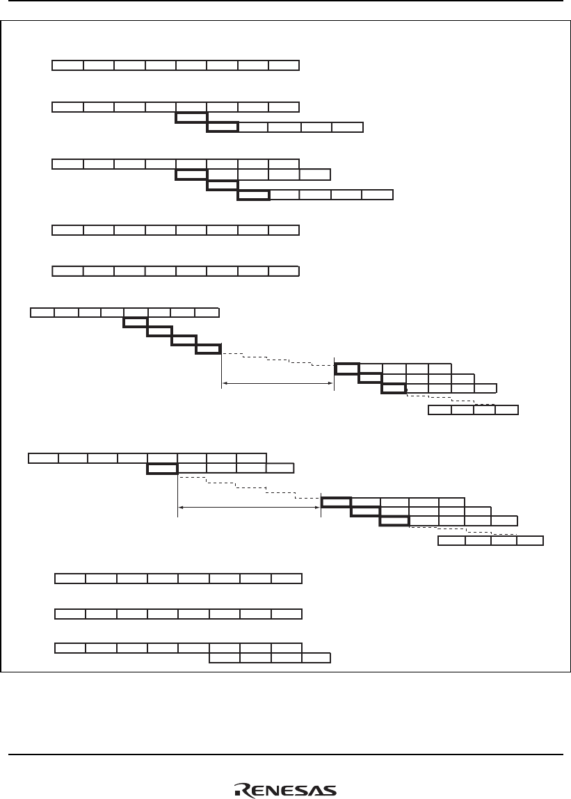
4. Pipelining
Rev.1.00 Jan. 10, 2008 Page 69 of 1658
REJ09B0261-0100
I1 I2 I3 ID S1 S2 S3 WB
I3
I3
I3
I3
I1 I2 ID S1 S2 S3 WB
I1 I2 ID S1 S2 S3 WB
E2S2 E3S3 WB
E1S1
I1 I2 ID S1 S2 S3 WB
E2S2 E3S3 WBE1S1
E2S2 E3S3 WB
E1S1
E2s2 E3s3
E1s1
I1 I2 ID WB
I1 I2 I3 ID s1 s2 s3 WB
I1 I2 I3 ID S1 S2 S3 WB
I3
I3
I1 I2 ID S1 S2 S3 WB
I1 I2 ID S1 S2 S3 WB
S1 S2 S3 WB
ID
ID
ID
ID
ID
E1s1 E2s2 E3s3 WB
ID
E1s1
E1s1
E1s1
E2s2
E2s2
E2s2
E3s3
E3s3
E3s3
WB
WB
WB
(I1) (ID)(I2) (I3)
I1 I2 I3 ID s1 s2 s3 WB
E1s1
E1s1
E1s1
E2s2
E2s2
E2s2
E3s3
E3s3
E3s3
WB
WB
WB
(I1) (ID)(I2) (I3)
ID
ID
ID
ID
ID
ID
ID
ID
ID
ID
(3-1) Load/store: 1 issue cycle
(3-2) AND.B, OR.B, XOR.B, TST.B: 3 issue cycles
(3-3) TAS.B: 4 issue cycles
(3-4) PREF, OCBI, OCBP, OCBWB, MOVCA.L, SYNCO: 1 issue cycle
MOV.[BWL], MOV.[BWL] @(d,GBR)
(3-5) LDTLB: 1 issue cycle
(3-6) ICBI: 8 issue cycles + 5 cycles + 4 branch cycle
(3-7) PREFI: 5 issue cycles + 5 cycles + 4 branch cycle
(3-8) MOVLI.L: 1 issue cycle
(3-9) MOVCO.L: 1 issue cycle
(3-10) MOVUA.L: 2 issue cycles
(Branch to the next instruction of ICBI.)
5 cycles (min.)
(Branch to the next instruction of PREFI.)
5 cycles (min.)
Figure 4.2 Instruction Execution Patterns (3)
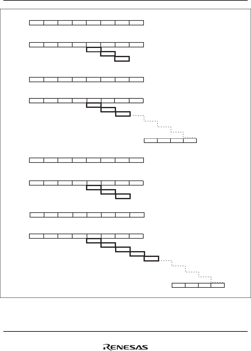
4. Pipelining
Rev.1.00 Jan. 10, 2008 Page 70 of 1658
REJ09B0261-0100
I1 I2 I3 ID s1 s2 s3 WB
I3
I3
I3
I3
I3
I3
I3
I1 I2 ID s1 s2 s3 WB
I1 I2 ID s1 s2 s3 WB
I1 I2 ID S1 S2 S3 WB
I1 I2 ID E1s1 E2s2 E3s3 WB
I1 I2 ID S1 S2 S3 WB
ID
ID
ID
I1 I2 ID E1S1 E2S2 E3S3 WB
ID
ID
ID
ID
ID
I1 I2 ID S1 S2 S3 WB
(I1) (ID)(I2) (I3)
(I1) (ID)(I2) (I3)
ID
ID
ID
ID
ID
ID
(4-1) LDC to Rp_BANK/SSR/SPC/VBR: 1 issue cycle
(4-2) LDC to DBR/SGR: 4 issue cycles
(4-3) LDC to GBR: 1 issue cycle
(4-4) LDC to SR: 4 issue cycles + 4 branch cycles
(4-5) LDC.L to Rp_BANK/SSR/SPC/VBR: 1 issue cycle
(4-6) LDC.L to DBR/SGR: 4 issue cycles
(4-7) LDC.L to GBR: 1 issue cycle
(4-8) LDC.L to SR: 6 issue cycles + 4 branch cycles
(Branch to the
next instruction.)
(Branch to the next instruction.)
Figure 4.2 Instruction Execution Patterns (4)
4. Pipelining
Rev.1.00 Jan. 10, 2008 Page 71 of 1658
REJ09B0261-0100
I1 I2 I3 ID s1 s2 s3 WB
I3
I3
I3
I3
I3
I3
I3
I1 I2 ID WB
I1 I2 ID S1 S2 S3
E1s1 E2s2 E3s3
WB
I1 I2 ID WB
I1 I2 ID S1 S2 S3
E1S1 E2S2 E3S3
WB
I1 I2 ID s1 s2 s3 WB
I1 I2 ID s1 s2 s3 WB
I1 I2 ID S1 S2 S3 WB
(I1) (I2) (I3) (ID) (??1) (??2) (??3) (WB)
(4-9) STC from DBR/GBR/Rp_BANK/SSR/SPC/VBR/SGR: 1 issue cycle
(4-10) STC from SR: 1 issue cycle
(4-11) STC.L from DBR/GBR/Rp_BANK/SSR/SPC/VBR/SGR: 1 issue cycle
(4-12) STC.L from SR: 1 issue cycle
(4-13) LDS to PR: 1 issue cycle
(4-14) LDS.L to PR: 1 issue cycle
(4-15) STS from PR: 1 issue cycle
(4-16) STS.L from PR: 1 issue cycle
(4-17) BSRF, BSR, JSR delay slot instructions (PR set): 0 issue cycle
The value of PR is changed in the E3 stage of delay slot instruction.
When the STS and STS.L instructions from PR are used as delay slot instructions,
changed PR value is used.
Notes:
Figure 4.2 Instruction Execution Patterns (5)
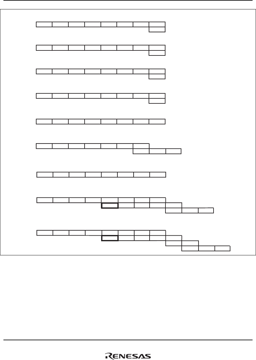
4. Pipelining
Rev.1.00 Jan. 10, 2008 Page 72 of 1658
REJ09B0261-0100
I1 I2 I3 ID s1 s2 s3 WB
MS
I3
I3
I3
I3
I3
I3
I3
I3
I1 I2 ID E1 M2 M3
E1 M2 M3
MS
E1 M2 M3 MS
M2 M3 MS
I1 I2 ID
I1 I2 ID S1 S2 S3 WB
S1 S2 S3 WB
I1 I2 ID
I1 I2 ID s1 s2 s3 WB
MS
I1 I2 ID S1 S2 S3 WB
MS
I1 I2 ID S1 S2 S3 WB
MS
M2 M3 MS
M2 M3 MS
M2 M3
I1 I2 ID S1 S2 S3 WB
S1 S2 S3 WB
ID
ID
(5-1) LDS to MACH/L: 1 issue cycle
(5-2) LDS.L to MACH/L: 1 issue cycle
(5-3) STS from MACH/L: 1 issue cycle
(5-4) STS.L from MACH/L: 1 issue cycle
(5-5) MULS.W, MULU.W: 1 issue cycle
(5-6) DMULS.L, DMULU.L, MUL.L: 1 issue cycle
(5-7) CLRMAC: 1 issue cycle
(5-8) MAC.W: 2 issue cycle
(5-9) MAC.L: 2 issue cycle
Figure 4.2 Instruction Execution Patterns (6)
4. Pipelining
Rev.1.00 Jan. 10, 2008 Page 73 of 1658
REJ09B0261-0100
I1 I2 I3 ID s1 s2 s3
s1 s2 s3 WB
s1 s2 s3 WB
FS1 FS2 FS3 FS4
FS1 FS2 FS3 FS4
FS
FS1 FS2 FS3 FS4
FS1 FS2 FS3 FS4
FS1 FS2 FS3 FS4
FS
FS1 FS2 FS3 FS4 FS
FS1 FS2 FS3 FS4
FS1 FS2 FS3 FS4
FS
FS1 FS2 FS3 FS4 FS
I3
I3
I3
I3
I3
I3
I3
I3
I3
I3
I1 I2 ID
I1 I2 ID S1 S2 S3 WB
S1 S2 S3
S1 S2 S3
WB
I1 I2 ID s1 s2 s3
I1 I2 ID WB
S1 S2 S3 WB
FS1 FS2 FS3 FS4
S1 S2 S3 WB
FS1 FS2 FS3 FS4 FS
s1 s2 s3 WB
I1 I2 ID
I1 I2 ID
I1 I2 ID
I1 I2 ID
I1 I2 ID
I1 I2 ID
s1 s2 s3
FS
(6-1) LDS to FPUL: 1 issue cycle
(6-2) STS from FPUL: 1 issue cycle
(6-3) LDS.L to FPUL: 1 issue cycle
(6-4) STS.L from FPUL: 1 issue cycle
(6-5) LDS to FPSCR: 1 issue cycle
(6-6) STS from FPSCR: 1 issue cycle
(6-7) LDS.L to FPSCR: 1 issue cycle
(6-8) STS.L from FPSCR: 1 issue cycle
(6-9) FPU load/store instruction FMOV: 1 issue cycle
(6-10) FLDS: 1 issue cycle
(6-11) FSTS: 1 issue cycle
Figure 4.2 Instruction Execution Patterns (7)
4. Pipelining
Rev.1.00 Jan. 10, 2008 Page 74 of 1658
REJ09B0261-0100
I1 I2 I3 ID s1 s2 s3
FS1 FS2 FS3 FS4 FS
I1 I2 I3 ID
I1 I2 I3 ID s1 s2 s3
FS1 FS2 FS3 FS4
FE1 FE2 FE3 FE4 FE5 FE6 FS
I1 I2 I3 ID FE1 FE2 FE3 FE4 FE5 FE6 FS
FE1 FE2 FE3 FE4 FE5 FE6
FE1 FE2 FE3 FE4 FE5 FE6
FS
FE1 FE2 FE3 FE4 FE5 FE6 FS
FE3 FE4 FE5 FE6 FS
FE3 FE4 FE5 FE6 FS
FE1 FE2 FE3 FE4 FE5 FE6 FS
I1 I2 I3 ID
I1 I2 I3 ID FE1 FE2 FE3 FE4 FE5 FE6 FS
FE3 FE4 FE5 FE6 FS
FS
I1 I2 I3 ID FS
(6-12) Single-precision FABS, FNEG/double-precision FABS, FNEG: 1 issue cycle
(6-13) FLDI0, FLDI1: 1 issue cycle
(6-14) Single-precision floating-point computation: 1 issue cycle
(6-15) Single-precision FDIV/FSQRT: 1 issue cycle
(6-16) Double-precision floating-point computation: 1 issue cycle
(6-17) Double-precision floating-point computation: 1 issue cycle
(6-18) Double-precision FDIV/FSQRT: 1 issue cycle
FEDS (Divider occupied cycle)
FCMP/EQ, FCMP/GT, FADD, FLOAT, FMAC, FMUL, FSUB, FTRC, FRCHG, FSCHG, FPCHG
FCMP/EQ, FCMP/GT, FADD, FLOAT, FSUB, FTRC, FCNVSD, FCNVDS
FMUL
FEDS (Divider occupied cycle)
Figure 4.2 Instruction Execution Patterns (8)
4. Pipelining
Rev.1.00 Jan. 10, 2008 Page 75 of 1658
REJ09B0261-0100
I1 I2 I3 ID FE1 FE2 FE3
FEPL
FEPL
FE4 FE5 FE6 FS
I1 I2 I3 ID FE1 FE2 FE3 FE4 FE5 FE6 FS
I1 I2 I3 ID FE1 FE2
FE1 FE2
FE3 FE4 FE5 FE6 FS
FE3 FE4 FE5 FE6 FS
FE1 FE2 FE3 FE4 FE5 FE6 FS
FE1 FE2 FE3 FE4 FE5 FE6
I1 I2 I3 ID FE1 FE2
FE1 FE2
FE3 FE4 FE5 FE6 FS
FE3 FE4 FE5 FE6 FS
FE1 FE2 FE3 FE4 FE5 FE6
FS
FS
(6-19) FIPR: 1 issue cycle
(6-20) FTRV: 1 issue cycle
(6-21) FSRRA: 1 issue cycle
(6-22) FSCA: 1 issue cycle
Function computing unit occupied cycle
Function computing unit occupied cycle
Figure 4.2 Instruction Execution Patterns (9)

4. Pipelining
Rev.1.00 Jan. 10, 2008 Page 76 of 1658
REJ09B0261-0100
4.2 Parallel-Executability
Instructions are categorized into six groups according to the internal function blocks used, as
shown in table 4.2. Table 4.3 shows the parallel-executability of pairs of instructions in terms of
groups. For example, ADD in the EX group and BRA in the BR group can be executed in parallel.
Table 4.2 Instruction Groups
Instruction
Group Instruction
EX ADD
ADDC
ADDV
AND #imm,R0
AND Rm,Rn
CLRMAC
CLRS
CLRT
CMP
DIV0S
DIV0U
DIV1
DMUS.L
DMULU.L
DT
EXTS
EXTU
MOVT
MUL.L
MULS.W
MULU.W
NEG
NEGC
NOT
OR #imm,R0
OR Rm,Rn
ROTCL
ROTCR
ROTL
ROTR
SETS
SETT
SHAD
SHAL
SHAR
SHLD
SHLL
SHLL2
SHLL8
SHLL16
SHLR
SHLR2
SHLR8
SHLR16
SUB
SUBC
SUBV
SWAP
TST #imm,R0
TST Rm,Rn
XOR #imm,R0
XOR Rm,Rn
XTRCT
MT MOV #imm,Rn MOV Rm,Rn NOP
BR BF
BF/S
BRA
BRAF
BSR
BSRF
BT
BT/S
JMP
JSR
RTS
LS FABS
FNEG
FLDI0
FLDI1
FLDS
FMOV @adr,FR
FMOV FR,@adr
FMOV FR,FR
FMOV.S @adr,FR
FMOV.S FR,@adr
FSTS
LDC Rm,CR1
LDC.L @Rm+,CR1
LDS Rm,SR1
LDS Rm,SR2
LDS.L @adr,SR2
LDS.L @Rm+,SR1
LDS.L @Rm+,SR2
MOV.[BWL] @adr,R
MOV.[BWL] R,@adr
MOVA
MOVCA.L
MOVUA
OCBI
OCBP
OCBWB
PREF
STC CR2,Rn
STC.L CR2,@-Rn
STS SR2,Rn
STS.L SR2,@-Rn
STS SR1,Rn
STS.L SR1,@-Rn

4. Pipelining
Rev.1.00 Jan. 10, 2008 Page 77 of 1658
REJ09B0261-0100
Instruction
Group Instruction
FE FADD
FSUB
FCMP (S/D)
FCNVDS
FCNVSD
FDIV
FIPR
FLOAT
FMAC
FMUL
FRCHG
FSCHG
FSQRT
FTRC
FTRV
FSCA
FSRRA
FPCHG
CO AND.B #imm,@(R0,GBR)
ICBI
LDC Rm,DBR
LDC Rm, SGR
LDC Rm,SR
LDC.L @Rm+,DBR
LDC.L @Rm+,SGR
LDC.L @Rm+,SR
LDTLB
MAC.L
MAC.W
MOVCO
MOVLI
OR.B #imm,@(R0,GBR)
PREFI
RTE
SLEEP
STC SR,Rn
STC.L SR,@-Rn
SYNCO
TAS.B
TRAPA
TST.B #imm,@(R0,GBR)
XOR.B #imm,@(R0,GBR)
Legend:
R: Rm/Rn
@adr: Address
SR1: MACH/MACL/PR
SR2: FPUL/FPSCR
CR1: GBR/Rp_BANK/SPC/SSR/VBR
CR2: CR1/DBR/SGR
FR: FRm/FRn/DRm/DRn/XDm/XDn
The parallel execution of two instructions can be carried out under following conditions.
1. Both addr (preceding instruction) and addr+2 (following instruction) are specified within the
minimum page size (1 Kbyte).
2. The execution of these two instructions is supported in table 4.3, Combination of Preceding
and Following Instructions.
3. Data used by an instruction of addr does not conflict with data used by a previous instruction
4. Data used by an instruction of addr+2 does not conflict with data used by a previous
instruction
5. Both instructions are valid

4. Pipelining
Rev.1.00 Jan. 10, 2008 Page 78 of 1658
REJ09B0261-0100
Table 4.3 Combination of Preceding and Following Instructions
Preceding Instruction (addr)
EX MT BR LS FE CO
EX No Yes Yes Yes Yes
MT Yes Yes Yes Yes Yes
Following
Instruction
(addr+2) BR Yes Yes No Yes Yes
LS Yes Yes Yes No Yes
FE Yes Yes Yes Yes No
CO No
4. Pipelining
Rev.1.00 Jan. 10, 2008 Page 79 of 1658
REJ09B0261-0100
4.3 Issue Rates and Execution Cycles
Instruction execution cycles are summarized in table 4.4. Instruction Group in the table 4.4
corresponds to the category in the table 4.2. Penalty cycles due to a pipeline stall are not
considered in the issue rates and execution cycles in this section.
I1 I2 I3 ID S1 S2 S3 WB
E2S2 E3S3 WB
E1S1
I1 I2 I3 ID S1 S2 S3 WB
MS
S2 S3 WB
S1
ID
ID
ID
(I1) (ID)(I2) (I3)
M3
M2
(I1) (I3) (ID)(I2)
I1 I2 I3 ID S1 S2 S3 WB
E2S2 E3S3 WB
E1S1
ID
ID
I1 I2 I3 ID S1 S2 S3 WB
MS
S2 S3 WB
S1
ID
M3
M2
FE1 FE2 FE3 FE4 FE5 FE6
FE1 FE2 FE3 FE4 FE5 FE6
FS
FE1 FE2 FE3 FE4 FE5 FE6 FS
FE1 FE2 FE3 FE4 FE5 FE6 FS
I1 I2 I3 ID
I1 I2 I3 ID FS
FE3 FE4 FE5 FE6 FS
1. Issue Rate
Issue rate: 3
Issue rates indicates the issue period between one instruction and next instruction.
E.g. AND.B instruction
Next instruction
Issue rate: 2
E.g. MAC.W instruction
Execution cycles indicates the cycle counts an instruction occupied the pipeline based on the next rules.
CPU instruction
E.g. AND.B instruction Execution Cycles: 3
E.g. MAC.W instruction Execution Cycles: 4
2. Execution Cycles
Next instruction
FPU instruction
E.g. FMUL instruction
Execution Cycles: 14
E.g. FDIV instruction
Execution Cycles: 3
Divider occupation cycle

4. Pipelining
Rev.1.00 Jan. 10, 2008 Page 80 of 1658
REJ09B0261-0100
Table 4.4 Issue Rates and Execution Cycles
Functional
Category No. Instruction
Instruction
Group Issue Rate
Execution
Cycles
Execution
Pattern
1 EXTS.B Rm,Rn EX 1 1 2-1
2 EXTS.W Rm,Rn EX 1 1 2-1
3 EXTU.B Rm,Rn EX 1 1 2-1
4 EXTU.W Rm,Rn EX 1 1 2-1
5 MOV Rm,Rn MT 1 1 2-4
6 MOV #imm,Rn MT 1 1 2-3
7 MOVA @(disp,PC),R0 LS 1 1 2-2
8 MOV.W @(disp,PC),Rn LS 1 1 3-1
9 MOV.L @(disp,PC),Rn LS 1 1 3-1
10 MOV.B @Rm,Rn LS 1 1 3-1
11 MOV.W @Rm,Rn LS 1 1 3-1
12 MOV.L @Rm,Rn LS 1 1 3-1
13 MOV.B @Rm+,Rn LS 1 1 3-1
14 MOV.W @Rm+,Rn LS 1 1 3-1
15 MOV.L @Rm+,Rn LS 1 1 3-1
16 MOV.B @(disp,Rm),R0 LS 1 1 3-1
17 MOV.W @(disp,Rm),R0 LS 1 1 3-1
18 MOV.L @(disp,Rm),Rn LS 1 1 3-1
19 MOV.B @(R0,Rm),Rn LS 1 1 3-1
20 MOV.W @(R0,Rm),Rn LS 1 1 3-1
21 MOV.L @(R0,Rm),Rn LS 1 1 3-1
22 MOV.B @(disp,GBR),R0 LS 1 1 3-1
23 MOV.W @(disp, GBR),R0 LS 1 1 3-1
24 MOV.L @(disp, GBR),R0 LS 1 1 3-1
25 MOV.B Rm,@Rn LS 1 1 3-1
26 MOV.W Rm,@Rn LS 1 1 3-1
27 MOV.L Rm,@Rn LS 1 1 3-1
28 MOV.B Rm,@-Rn LS 1 1 3-1
Data transfer
instructions
29 MOV.W Rm,@-Rn LS 1 1 3-1

4. Pipelining
Rev.1.00 Jan. 10, 2008 Page 81 of 1658
REJ09B0261-0100
Functional
Category No. Instruction
Instruction
Group Issue Rate
Execution
Cycles
Execution
Pattern
30 MOV.L Rm,@-Rn LS 1 1 3-1
31 MOV.B R0,@(disp,Rn) LS 1 1 3-1
32 MOV.W R0,@(disp,Rn) LS 1 1 3-1
33 MOV.L Rm,@(disp,Rn) LS 1 1 3-1
34 MOV.B Rm,@(R0,Rn) LS 1 1 3-1
35 MOV.W Rm,@(R0,Rn) LS 1 1 3-1
36 MOV.L Rm,@(R0,Rn) LS 1 1 3-1
37 MOV.B R0,@(disp,GBR) LS 1 1 3-1
38 MOV.W R0,@(disp,GBR) LS 1 1 3-1
39 MOV.L R0,@(disp,GBR) LS 1 1 3-1
40 MOVCA.L R0,@Rn LS 1 1 3-4
41 MOVCO.L R0,@Rn CO 1 1 3-9
42 MOVLI.L @Rm,R0 CO 1 1 3-8
43 MOVUA.L @Rm,R0 LS 2 2 3-10
44 MOVUA.L @Rm+,R0 LS 2 2 3-10
45 MOVT Rn EX 1 1 2-1
46 OCBI @Rn LS 1 1 3-4
47 OCBP @Rn LS 1 1 3-4
48 OCBWB @Rn LS 1 1 3-4
49 PREF @Rn LS 1 1 3-4
50 SWAP.B Rm,Rn EX 1 1 2-1
51 SWAP.W Rm,Rn EX 1 1 2-1
Data transfer
instructions
52 XTRCT Rm,Rn EX 1 1 2-1
53 ADD Rm,Rn EX 1 1 2-1
54 ADD #imm,Rn EX 1 1 2-1
55 ADDC Rm,Rn EX 1 1 2-1
56 ADDV Rm,Rn EX 1 1 2-1
57 CMP/EQ #imm,R0 EX 1 1 2-1
Fixed-point
arithmetic
instructions
58 CMP/EQ Rm,Rn EX 1 1 2-1
59 CMP/GE Rm,Rn EX 1 1 2-1

4. Pipelining
Rev.1.00 Jan. 10, 2008 Page 82 of 1658
REJ09B0261-0100
Functional
Category No. Instruction
Instruction
Group Issue Rate
Execution
Cycles
Execution
Pattern
60 CMP/GT Rm,Rn EX 1 1 2-1
61 CMP/HI Rm,Rn EX 1 1 2-1
62 CMP/HS Rm,Rn EX 1 1 2-1
63 CMP/PL Rn EX 1 1 2-1
64 CMP/PZ Rn EX 1 1 2-1
65 CMP/STR Rm,Rn EX 1 1 2-1
66 DIV0S Rm,Rn EX 1 1 2-1
67 DIV0U EX 1 1 2-1
68 DIV1 Rm,Rn EX 1 1 2-1
69 DMULS.L Rm,Rn EX 1 2 5-6
70 DMULU.L Rm,Rn EX 1 2 5-6
71 DT Rn EX 1 1 2-1
72 MAC.L @Rm+,@Rn+ CO 2 5 5-9
73 MAC.W @Rm+,@Rn+ CO 2 4 5-8
74 MUL.L Rm,Rn EX 1 2 5-6
75 MULS.W Rm,Rn EX 1 1 5-5
76 MULU.W Rm,Rn EX 1 1 5-5
77 NEG Rm,Rn EX 1 1 2-1
78 NEGC Rm,Rn EX 1 1 2-1
79 SUB Rm,Rn EX 1 1 2-1
80 SUBC Rm,Rn EX 1 1 2-1
Fixed-point
arithmetic
instructions
81 SUBV Rm,Rn EX 1 1 2-1
82 AND Rm,Rn EX 1 1 2-1
83 AND #imm,R0 EX 1 1 2-1
84 AND.B #imm,@(R0,GBR) CO 3 3 3-2
85 NOT Rm,Rn EX 1 1 2-1
86 OR Rm,Rn EX 1 1 2-1
87 OR #imm,R0 EX 1 1 2-1
Logical
instructions
88 OR.B #imm,@(R0,GBR) CO 3 3 3-2
89 TAS.B @Rn CO 4 4 3-3

4. Pipelining
Rev.1.00 Jan. 10, 2008 Page 83 of 1658
REJ09B0261-0100
Functional
Category No. Instruction
Instruction
Group Issue Rate
Execution
Cycles
Execution
Pattern
90 TST Rm,Rn EX 1 1 2-1
91 TST #imm,R0 EX 1 1 2-1
92 TST.B #imm,@(R0,GBR) CO 3 3 3-2
93 XOR Rm,Rn EX 1 1 2-1
94 XOR #imm,R0 EX 1 1 2-1
Logical
instructions
95 XOR.B #imm,@(R0,GBR) CO 3 3 3-2
96 ROTL Rn EX 1 1 2-1
97 ROTR Rn EX 1 1 2-1
98 ROTCL Rn EX 1 1 2-1
99 ROTCR Rn EX 1 1 2-1
100 SHAD Rm,Rn EX 1 1 2-1
101 SHAL Rn EX 1 1 2-1
102 SHAR Rn EX 1 1 2-1
103 SHLD Rm,Rn EX 1 1 2-1
104 SHLL Rn EX 1 1 2-1
105 SHLL2 Rn EX 1 1 2-1
106 SHLL8 Rn EX 1 1 2-1
107 SHLL16 Rn EX 1 1 2-1
108 SHLR Rn EX 1 1 2-1
109 SHLR2 Rn EX 1 1 2-1
110 SHLR8 Rn EX 1 1 2-1
Shift
instructions
111 SHLR16 Rn EX 1 1 2-1
112 BF disp BR 1+0 to 2 1 1-1
113 BF/S disp BR 1+0 to 2 1 1-1
114 BT disp BR 1+0 to 2 1 1-1
115 BT/S disp BR 1+0 to 2 1 1-1
116 BRA disp BR 1+0 to 2 1 1-1
117 BRAF Rm BR 1+3 1 1-2
Branch
instructions
118 BSR disp BR 1+0 to 2 1 1-1
119 BSRF Rm BR 1+3 1 1-2

4. Pipelining
Rev.1.00 Jan. 10, 2008 Page 84 of 1658
REJ09B0261-0100
Functional
Category No. Instruction
Instruction
Group Issue Rate
Execution
Cycles
Execution
Pattern
120 JMP @Rn BR 1+3 1 1-2
121 JSR @Rn BR 1+3 1 1-2
Branch
instructions
122 RTS BR 1+0 to 3 1 1-3
123 NOP MT 1 1 2-3
124 CLRMAC EX 1 1 5-7
125 CLRS EX 1 1 2-1
126 CLRT EX 1 1 2-1
127 ICBI @Rn CO 8+5+3 13 3-6
128 SETS EX 1 1 2-1
129 SETT EX 1 1 2-1
130 PREFI @Rn CO 5+5+3 10 3-7
131 SYNCO CO Undefined Undefined 3-4
132 TRAPA #imm CO 8+5+1 13 1-5
133 RTE CO 4+1 4 1-4
134 SLEEP CO Undefined Undefined 1-6
135 LDTLB CO 1 1 3-5
136 LDC Rm,DBR CO 4 4 4-2
137 LDC Rm,SGR CO 4 4 4-2
138 LDC Rm,GBR LS 1 1 4-3
139 LDC Rm,Rp_BANK LS 1 1 4-1
140 LDC Rm,SR CO 4+3 4 4-4
141 LDC Rm,SSR LS 1 1 4-1
142 LDC Rm,SPC LS 1 1 4-1
143 LDC Rm,VBR LS 1 1 4-1
144 LDC.L @Rm+,DBR CO 4 4 4-6
145 LDC.L @Rm+,SGR CO 4 4 4-6
146 LDC.L @Rm+,GBR LS 1 1 4-7
147 LDC.L @Rm+,Rp_BANK LS 1 1 4-5
System
control
instruction
148 LDC.L @Rm+,SR CO 6+3 4 4-8
149 LDC.L @Rm+,SSR LS 1 1 4-5

4. Pipelining
Rev.1.00 Jan. 10, 2008 Page 85 of 1658
REJ09B0261-0100
Functional
Category No. Instruction
Instruction
Group Issue Rate
Execution
Cycles
Execution
Pattern
150 LDC.L @Rm+,SPC LS 1 1 4-5
151 LDC.L @Rm+,VBR LS 1 1 4-5
152 LDS Rm,MACH LS 1 1 5-1
153 LDS Rm,MACL LS 1 1 5-1
154 LDS Rm,PR LS 1 1 4-13
155 LDS.L @Rm+,MACH LS 1 1 5-2
156 LDS.L @Rm+,MACL LS 1 1 5-2
157 LDS.L @Rm+,PR LS 1 1 4-14
158 STC DBR,Rn LS 1 1 4-9
159 STC SGR,Rn LS 1 1 4-9
160 STC GBR,Rn LS 1 1 4-9
161 STC Rp_BANK,Rn LS 1 1 4-9
162 STC SR,Rn CO 1 1 4-10
163 STC SSR,Rn LS 1 1 4-9
164 STC SPC,Rn LS 1 1 4-9
165 STC VBR,Rn LS 1 1 4-9
166 STC.L DBR,@-Rn LS 1 1 4-11
167 STC.L SGR,@-Rn LS 1 1 4-11
168 STC.L GBR,@-Rn LS 1 1 4-11
169 STC.L Rp_BANK,@-Rn LS 1 1 4-11
170 STC.L SR,@-Rn CO 1 1 4-12
171 STC.L SSR,@-Rn LS 1 1 4-11
172 STC.L SPC,@-Rn LS 1 1 4-11
173 STC.L VBR,@-Rn LS 1 1 4-11
174 STS MACH,Rn LS 1 1 5-3
175 STS MACL,Rn LS 1 1 5-3
176 STS PR,Rn LS 1 1 4-15
System
control
instructions
177 STS.L MACH,@-Rn LS 1 1 5-4
178 STS.L MACL,@-Rn LS 1 1 5-4
179 STS.L PR,@-Rn LS 1 1 4-16

4. Pipelining
Rev.1.00 Jan. 10, 2008 Page 86 of 1658
REJ09B0261-0100
Functional
Category No. Instruction
Instruction
Group Issue Rate
Execution
Cycles
Execution
Pattern
180 FLDI0 FRn LS 1 1 6-13
181 FLDI1 FRn LS 1 1 6-13
182 FMOV FRm,FRn LS 1 1 6-9
183 FMOV.S @Rm,FRn LS 1 1 6-9
184 FMOV.S @Rm+,FRn LS 1 1 6-9
185 FMOV.S @(R0,Rm),FRn LS 1 1 6-9
186 FMOV.S FRm,@Rn LS 1 1 6-9
187 FMOV.S FRm,@-Rn LS 1 1 6-9
188 FMOV.S FRm,@(R0,Rn) LS 1 1 6-9
189 FLDS FRm,FPUL LS 1 1 6-10
190 FSTS FPUL,FRn LS 1 1 6-11
191 FABS FRn LS 1 1 6-12
192 FADD FRm,FRn FE 1 1 6-14
193 FCMP/EQ FRm,FRn FE 1 1 6-14
194 FCMP/GT FRm,FRn FE 1 1 6-14
195 FDIV FRm,FRn FE 1 14 6-15
196 FLOAT FPUL,FRn FE 1 1 6-14
197 FMAC FR0,FRm,FRn FE 1 1 6-14
198 FMUL FRm,FRn FE 1 1 6-14
199 FNEG FRn LS 1 1 6-12
200 FSQRT FRn FE 1 30 6-15
201 FSUB FRm,FRn FE 1 1 6-14
202 FTRC FRm,FPUL FE 1 1 6-14
203 FMOV DRm,DRn LS 1 1 6-9
204 FMOV @Rm,DRn LS 1 1 6-9
205 FMOV @Rm+,DRn LS 1 1 6-9
206 FMOV @(R0,Rm),DRn LS 1 1 6-9
Single-
precision
floating-point
instructions
207 FMOV DRm,@Rn LS 1 1 6-9
208 FMOV DRm,@-Rn LS 1 1 6-9
209 FMOV DRm,@(R0,Rn) LS 1 1 6-9

4. Pipelining
Rev.1.00 Jan. 10, 2008 Page 87 of 1658
REJ09B0261-0100
Functional
Category No. Instruction
Instruction
Group Issue Rate
Execution
Cycles
Execution
Pattern
210 FABS DRn LS 1 1 6-12
211 FADD DRm,DRn FE 1 1 6-16
212 FCMP/EQ DRm,DRn FE 1 1 6-16
213 FCMP/GT DRm,DRn FE 1 1 6-16
214 FCNVDS DRm,FPUL FE 1 1 6-16
215 FCNVSD FPUL,DRn FE 1 1 6-16
216 FDIV DRm,DRn FE 1 14 6-18
217 FLOAT FPUL,DRn FE 1 1 6-16
218 FMUL DRm,DRn FE 1 3 6-17
219 FNEG DRn LS 1 1 6-12
220 FSQRT DRn FE 1 30 6-18
221 FSUB DRm,DRn FE 1 1 6-16
Double-
precision
floating-point
instructions
222 FTRC DRm,FPUL FE 1 1 6-16
223 LDS Rm,FPUL LS 1 1 6-1
224 LDS Rm,FPSCR LS 1 1 6-5
225 LDS.L @Rm+,FPUL LS 1 1 6-3
226 LDS.L @Rm+,FPSCR LS 1 1 6-7
227 STS FPUL,Rn LS 1 1 6-2
228 STS FPSCR,Rn LS 1 1 6-6
229 STS.L FPUL,@-Rn LS 1 1 6-4
FPU system
control
instructions
230 STS.L FPSCR,@-Rn LS 1 1 6-8
231 FMOV DRm,XDn LS 1 1 6-9
232 FMOV XDm,DRn LS 1 1 6-9
233 FMOV XDm,XDn LS 1 1 6-9
234 FMOV @Rm,XDn LS 1 1 6-9
235 FMOV @Rm+,XDn LS 1 1 6-9
236 FMOV @(R0,Rm),XDn LS 1 1 6-9
237 FMOV XDm,@Rn LS 1 1 6-9
238 FMOV XDm,@-Rn LS 1 1 6-9
Graphics
acceleration
instructions
239 FMOV XDm,@(R0,Rn) LS 1 1 6-9
240 FIPR FVm,FVn FE 1 1 6-19

4. Pipelining
Rev.1.00 Jan. 10, 2008 Page 88 of 1658
REJ09B0261-0100
Functional
Category No. Instruction
Instruction
Group Issue Rate
Execution
Cycles
Execution
Pattern
241 FRCHG FE 1 1 6-14
242 FSCHG FE 1 1 6-14
243 FPCHG FE 1 1 6-14
244 FSRRA FRn FE 1 1 6-21
Graphics
acceleration
instructions
245 FSCA FPUL,DRn FE 1 3 6-22
246 FTRV XMTRX,FVn FE 1 4 6-20

5. Exception Handling
Rev.1.00 Jan. 10, 2008 Page 89 of 1658
REJ09B0261-0100
Section 5 Exception Handling
5.1 Summary of Exception Handling
Exception handling processing is handled by a special routine which is executed by a reset,
general exception handling, or interrupt. For example, if the executing instruction ends
abnormally, appropriate action must be taken in order to return to the original program sequence,
or report the abnormality before terminating the processing. The process of generating an
exception handling request in response to abnormal termination, and passing control to a user-
written exception handling routine, in order to support such functions, is given the generic name of
exception handling.
The exception handling in this LSI is of three kinds: resets, general exceptions, and interrupts.
5.2 Register Descriptions
Table 5.1 lists the configuration of registers related exception handling.
Table 5.1 Register Configuration
Register Name Abbr. R/W P4 Address*
Area 7
Address* Access Size
TRAPA exception register TRA R/W H'FF00 0020 H'1F00 0020 32
Exception event register EXPEVT R/W H'FF00 0024 H'1F00 0024 32
Interrupt event register INTEVT R/W H'FF00 0028 H'1F00 0028 32
Non-support detection exception
register
EXPMASK R/W H'FF2F 0004 H'1F2F 0004 32
Note: * P4 is the address when virtual address space P4 area is used. Area 7 is the address
when physical address space area 7 is accessed by using the TLB.
5. Exception Handling
Rev.1.00 Jan. 10, 2008 Page 90 of 1658
REJ09B0261-0100
Table 5.2 States of Register in Each Operating Mode
Register Name Abbr.
Power-on
Reset Manual Reset Sleep Standby
TRAPA exception register TRA Undefined Undefined Retained Retained
Exception event register EXPEVT H'0000 0000 H'0000 0020 Retained Retained
Interrupt event register INTEVT Undefined Undefined Retained Retained
Non-support detection exception
register
EXPMASK H'0000 0013 H'0000 0013 Retained Retained
5.2.1 TRAPA Exception Register (TRA)
The TRAPA exception register (TRA) consists of 8-bit immediate data (imm) for the TRAPA
instruction. TRA is set automatically by hardware when a TRAPA instruction is executed. TRA
can also be modified by software.
31 30 29 28 27 26 25 24 23 22 21 20 19 18 17 16
Bit:
0000000000000000
00
Initial value:
RRRRRRRRRRRRRRRR
R/W R/W R/W
TRACODE
R/W R/W R/W R R
R/W:
Bit:
Initial value:
R/W:
1514131211109876543210
000000
RRRRRRR/W
R/W
Bit Bit Name Initial Value R/W Description
31 to 10 ⎯ All 0 R Reserved
For details on reading/writing this bit, see General
Precautions on Handling of Product.
9 to 2 TRACODE Undefined R/W TRAPA Code
8-bit immediate data of TRAPA instruction is set
1, 0 ⎯ All 0 R Reserved
For details on reading/writing this bit, see General
Precautions on Handling of Product.

5. Exception Handling
Rev.1.00 Jan. 10, 2008 Page 91 of 1658
REJ09B0261-0100
5.2.2 Exception Event Register (EXPEVT)
The exception event register (EXPEVT) consists of a 12-bit exception code. The exception code
set in EXPEVT is that for a reset or general exception event. The exception code is set
automatically by hardware when an exception occurs. EXPEVT can also be modified by software.
31 30 29 28 27 26 25 24 23 22 21 20 19 18 17 16
Bit:
0000000000000000
0000000/100000
Initial value:
RRRRRRRRRRRRRRRR
R/W R/W
EXPCODE
R/W R/W R/W R/W R/W R/W
R/W:
Bit:
Initial value:
R/W:
1514131211109876543210
0000
R R R R R/W R/W R/W R/W
Bit Bit Name
Initial
Value R/W Description
31 to 12 ⎯ All 0 R Reserved
For details on reading/writing this bit, see General
Precautions on Handling of Product.
11 to 0 EXPCODE H'000 or
H'020
R/W Exception Code
The exception code for a reset or general exception is
set. For details, see table 5.3.
5. Exception Handling
Rev.1.00 Jan. 10, 2008 Page 92 of 1658
REJ09B0261-0100
5.2.3 Interrupt Event Register (INTEVT)
The interrupt event register (INTEVT) consists of a 14-bit exception code. The exception code is
set automatically by hardware when an exception occurs. INTEVT can also be modified by
software.
31 30 29 28 27 26 25 24 23 22 21 20 19 18 17 16
Bit:
0000000000000000
Initial value:
RRRRRRRRRRRRRRRR
R/W
INTCODE
R/W R/W R/W R/W R/W R/W R/W
R/W:
Bit:
Initial value:
R/W:
1514131211109876543210
00
R R R/W R/W R/W R/W R/W R/W
Bit Bit Name
Initial
Value R/W Description
31 to 14 ⎯ All 0 R Reserved
For details on reading/writing this bit, see General
Precautions on Handling of Product.
13 to 0 INTCODE Undefined R/W Exception Code
The exception code for an interrupt is set. For details,
see table 5.3.

5. Exception Handling
Rev.1.00 Jan. 10, 2008 Page 93 of 1658
REJ09B0261-0100
5.2.4 Non-Support Detection Exception Register (EXPMASK)
The non-support detection exception register (EXPMASK) is used to enable or disable the
generation of exceptions in response to the use of any of functions 1 to 3 listed below. The
functions of 1 to 3 are planned not to be supported in the future SuperH-family products. The
exception generation functions of EXPMASK can be used in advance of execution; the detection
function then checks for the use of these functions in the software. This will ease the transfer of
software to the future SuperH-family products that do not support the respective functions.
1. Handling of an instruction other than the NOP instruction in the delay slot of the RTE
instruction.
2. Handling of the SLEEP instruction in the delay slot of the branch instruction.
3. Performance of IC/OC memory-mapped associative write operations.
According to the value of EXPMASK, functions 1 and 2 can generate a slot illegal instruction
exception, and 3 can generate a data address error exception.
Generation of each exception can be disabled by writing 1 to the corresponding bit in EXPMASK.
However, it is recommended that the above functions should not be used when making a program
to maintain the compatibility with the future products.
Use the store instruction of the CPU to update EXPMASK. After updating the register and then
reading the register once, execute either of the following instructions. Executing either instruction
guarantees the operation with the updated register value.
• Execute the RTE instruction.
• Execute the ICBI instruction for any address (including non-cacheable area).
31 30 29 28 27 26 25 24 23 22 21 20 19 18 17 16
Bit:
Initial value:
R/W:
Bit:
Initial value:
R/W:
1514131211109876543210
0000000000000000
RRRRRRRRRRRRRRRR
0000000000010011
RRRRRRRRRRRR/WRRR/WR/W
−−−−−−−−−−−−
−−−−−−−−−−−
MM
CAW −−
BRDS
SLP RTE
DS
−−−−

5. Exception Handling
Rev.1.00 Jan. 10, 2008 Page 94 of 1658
REJ09B0261-0100
Bit Bit Name
Initial
Value R/W Description
31 to 5 ⎯ All 0 R Reserved
For details on reading/writing these bits, see General
Precautions on Handling of Product.
4 MMCAW 1 R/W Memory-Mapped Cache Associative Write
0: Memory-mapped cache associative write is disabled.
(A data address error exception will occur.)
1: Memory-mapped cache associative write is enabled.
For further details, refer to section 8.6.5, Memory-
Mapped Cache Associative Write Operation.
3, 2 ⎯ All 0 R Reserved
For details on reading/writing these bits, see General
Precautions on Handling of Product.
1 BRDSSLP 1 R/W Delay Slot SLEEP Instruction
0: The SLEEP instruction in the delay slot is disabled.
(The SLEEP instruction is taken as a slot illegal
instruction.)
1: The SLEEP instruction in the delay slot is enabled.
0 RTEDS 1 R/W RTE Delay Slot
0: An instruction other than the NOP instruction in the
delay slot of the RTE instruction is disabled. (An
instruction other than the NOP instruction is taken as
a slot illegal instruction).
1: An instruction other than the NOP instruction in the
delay slot of the RTE instruction is enabled.

5. Exception Handling
Rev.1.00 Jan. 10, 2008 Page 95 of 1658
REJ09B0261-0100
5.3 Exception Handling Functions
5.3.1 Exception Handling Flow
In exception handling, the contents of the program counter (PC), status register (SR), and R15 are
saved in the saved program counter (SPC), saved status register (SSR), and saved general
register15 (SGR), and the CPU starts execution of the appropriate exception handling routine
according to the vector address. An exception handling routine is a program written by the user to
handle a specific exception. The exception handling routine is terminated and control returned to
the original program by executing a return-from-exception instruction (RTE). This instruction
restores the PC and SR contents and returns control to the normal processing routine at the point at
which the exception occurred. The SGR contents are not written back to R15 with an RTE
instruction.
The basic processing flow is as follows. For the meaning of the SR bits, see section 2,
Programming Model.
1. The PC, SR, and R15 contents are saved in SPC, SSR, and SGR, respectively.
2. The block bit (BL) in SR is set to 1.
3. The mode bit (MD) in SR is set to 1.
4. The register bank bit (RB) in SR is set to 1.
5. In a reset, the FPU disable bit (FD) in SR is cleared to 0.
6. The exception code is written to bits 11 to 0 of the exception event register (EXPEVT) or
interrupt event register (INTEVT).
7. When the interrupt mode switch bit (INTMU) in CPUOPM has been 1, the interrupt mask
level bit (IMASK) in SR is changed to accepted interrupt level.
8. The CPU branches to the determined exception handling vector address, and the exception
handling routine begins.
5.3.2 Exception Handling Vector Addresses
The reset vector address is fixed at H'A0000000. Exception and interrupt vector addresses are
determined by adding the offset for the specific event to the vector base address, which is set by
software in the vector base register (VBR). In the case of the TLB miss exception, for example,
the offset is H'00000400, so if H'9C080000 is set in VBR, the exception handling vector address
will be H'9C080400. If a further exception occurs at the exception handling vector address, a
duplicate exception will result, and recovery will be difficult; therefore, addresses that are not to
be converted (in P1 and P2 areas) should be specified for vector addresses.

5. Exception Handling
Rev.1.00 Jan. 10, 2008 Page 96 of 1658
REJ09B0261-0100
5.4 Exception Types and Priorities
Table 5.3 shows the types of exceptions, with their relative priorities, vector addresses, and
exception/interrupt codes.
Table 5.3 Exceptions
Exception Transition
Direction*3
Exception
Category
Execution
Mode
Exception
Priority
Level*2
Priority
Order*2
Vector
Address Offset
Exception
Code*4
Power-on reset 1 1 H'A000 0000 — H'000
Manual reset 1 2 H'A000 0000 — H'020
H-UDI reset 1 1 H'A000 0000 — H'000
Instruction TLB multiple-hit
exception
1 3 H'A000 0000 — H'140
Reset Abort type
Data TLB multiple-hit exception 1 4 H'A000 0000 — H'140
User break before instruction
execution*1
2 0 (VBR/DBR) H'100/— H'1E0
Instruction address error 2 1 (VBR) H'100 H'0E0
Instruction TLB miss exception 2 2 (VBR) H'400 H'040
Instruction TLB protection
violation exception
2 3 (VBR) H'100 H'0A0
General illegal instruction
exception
2 4 (VBR) H'100 H'180
Slot illegal instruction exception 2 4 (VBR) H'100 H'1A0
General FPU disable exception 2 4 (VBR) H'100 H'800
Slot FPU disable exception 2 4 (VBR) H'100 H'820
Data address error (read) 2 5 (VBR) H'100 H'0E0
Data address error (write) 2 5 (VBR) H'100 H'100
Data TLB miss exception (read) 2 6 (VBR) H'400 H'040
Data TLB miss exception (write) 2 6 (VBR) H'400 H'060
Data TLB protection
violation exception (read)
2 7 (VBR) H'100 H'0A0
Data TLB protection
violation exception (write)
2 7 (VBR) H'100 H'0C0
General
exception
Re-
execution
type
FPU exception 2 8 (VBR) H'100 H'120
Initial page write exception 2 9 (VBR) H'100 H'080

5. Exception Handling
Rev.1.00 Jan. 10, 2008 Page 97 of 1658
REJ09B0261-0100
Exception Transition
Direction*3
Exception
Category
Execution
Mode
Exception
Priority
Level*2
Priority
Order*2
Vector
Address Offset
Exception
Code*4
Unconditional trap (TRAPA) 2 4 (VBR) H'100 H'160 General
exception
Completion
type User break after instruction
execution*
2 10 (VBR/DBR) H'100/— H'1E0
Nonmaskable interrupt 3 — (VBR) H'600 H'1C0 Interrupt Completion
type General interrupt request 4 — (VBR) H'600 —
Notes: 1. When UBDE in CBCR = 1, PC = DBR. In other cases, PC = VBR + H'100.
2. Priority is first assigned by priority level, then by priority order within each level (the
lowest number represents the highest priority).
3. Control passes to H'A000 0000 in a reset, and to [VBR + offset] in other cases.
4. Stored in EXPEVT for a reset or general exception, and in INTEVT for an interrupt.

5. Exception Handling
Rev.1.00 Jan. 10, 2008 Page 98 of 1658
REJ09B0261-0100
5.5 Exception Flow
5.5.1 Exception Flow
Figure 5.1 shows an outline flowchart of the basic operations in instruction execution and
exception handling. For the sake of clarity, the following description assumes that instructions are
executed sequentially, one by one. Figure 5.1 shows the relative priority order of the different
kinds of exceptions (reset, general exception, and interrupt). Register settings in the event of an
exception are shown only for SSR, SPC, SGR, EXPEVT/INTEVT, SR, and PC. However, other
registers may be set automatically by hardware, depending on the exception. For details, see
section 5.6, Description of Exceptions. Also, see section 5.6.4, Priority Order with Multiple
Exceptions, for exception handling during execution of a delayed branch instruction and a delay
slot instruction, or in the case of instructions in which two data accesses are performed.
5. Exception Handling
Rev.1.00 Jan. 10, 2008 Page 99 of 1658
REJ09B0261-0100
Execute next instruction
Is highest-
priority exception
re-exception
type? Cancel instruction execution
result
Yes
Yes
Yes
No
No
No
No
Yes
SSR ← SR
SPC ← PC
SGR ← R15
EXPEVT/INTEVT ← exception code
SR.{MD,RB,BL} ← 111
SR.IMASK ← received interuupt level (*)
PC ← (CBCR.UBDE=1 && User_Break?
DBR: (VBR + Offset))
Interrupt
requested?
General
exception requested?
Reset
requested?
EXPEVT ← exception code
SR. {MD, RB, BL, FD, IMASK} ← 11101111
PC ← H'A000 0000
Note: *When the exception of the highest priority is an interrupt.
Whether IMASK is updated or not can be set by software.
"Accepted interrupt level" is B'1111 for NMI.
Figure 5.1 Instruction Execution and Exception Handling
5. Exception Handling
Rev.1.00 Jan. 10, 2008 Page 100 of 1658
REJ09B0261-0100
5.5.2 Exception Source Acceptance
A priority ranking is provided for all exceptions for use in determining which of two or more
simultaneously generated exceptions should be accepted. Five of the general exceptions—general
illegal instruction exception, slot illegal instruction exception, general FPU disable exception, slot
FPU disable exception, and unconditional trap exception—are detected in the process of
instruction decoding, and do not occur simultaneously in the instruction pipeline. These
exceptions therefore all have the same priority. General exceptions are detected in the order of
instruction execution. However, exception handling is performed in the order of instruction flow
(program order). Thus, an exception for an earlier instruction is accepted before that for a later
instruction. An example of the order of acceptance for general exceptions is shown in figure 5.2.
I1
I1
ID
ID
E3
WB
WB
TLB miss (data access)
Pipeline flow:
Order of detection:
Instruction n
Instruction n + 1
General illegal instruction exception (instruction n + 1) and
TLB miss (instruction n + 2) are detected simultaneously
Order of exception handling:
TLB miss (instruction n)
Program order
1
Instruction n + 2
General illegal instruction exception
I1 ID WB
WB
TLB miss (instruction access)
2
3
4
I1, I2, I3: Instruction fetch
ID : Instruction decode
E1, E2, E3: Instruction execution
(E2, E3 Memory access)
WB Write-back
Instruction n + 3
TLB miss (instruction n)
Re-execution of instruction n
General illegal instruction exception
(instruction n + 1)
Re-execution of instruction n + 1
TLB miss (instruction n + 2)
Re-execution of instruction n + 2
Execution of instruction n + 3
Legend:
E3
E3
E2
E2
E1
E1
I2
I2
I3
I3
E1
E1 E2
E2 E3I2 I3
I3 IDI2I1
Figure 5.2 Example of General Exception Acceptance Order

5. Exception Handling
Rev.1.00 Jan. 10, 2008 Page 101 of 1658
REJ09B0261-0100
5.5.3 Exception Requests and BL Bit
When the BL bit in SR is 0, general exceptions and interrupts are accepted.
When the BL bit in SR is 1 and an general exception other than a user break is generated, the
CPU's internal registers and the registers of the other modules are set to their states following a
manual reset, and the CPU branches to the same address as in a reset (H'A0000000). For the
operation in the event of a user break, see section 29, User Break Controller (UBC). If an ordinary
interrupt occurs, the interrupt request is held pending and is accepted after the BL bit has been
cleared to 0 by software. If a nonmaskable interrupt (NMI) occurs, it can be held pending or
accepted according to the setting made by software. For further details, refer to the hardware
manual of the product.
Thus, normally, SPC and SSR are saved and then the BL bit in SR is cleared to 0, to enable
multiple exception state acceptance.
5.5.4 Return from Exception Handling
The RTE instruction is used to return from exception handling. When the RTE instruction is
executed, the SPC contents are restored to PC and the SSR contents to SR, and the CPU returns
from the exception handling routine by branching to the SPC address. If SPC and SSR were saved
to external memory, set the BL bit in SR to 1 before restoring the SPC and SSR contents and
issuing the RTE instruction.

5. Exception Handling
Rev.1.00 Jan. 10, 2008 Page 102 of 1658
REJ09B0261-0100
5.6 Description of Exceptions
The various exception handling operations explained here are exception sources, transition address
on the occurrence of exception, and processor operation when a transition is made.
5.6.1 Resets
(1) Power-On Reset
• Condition:
Power-on reset request
• Operations:
Exception code H'000 is set in EXPEVT, initialization of the CPU and on-chip peripheral
module is carried out, and then a branch is made to the reset vector (H'A0000000). For details,
see the register descriptions in the relevant sections. A power-on reset should be executed
when power is supplied.
(2) Manual Reset
• Condition:
Manual reset request
• Operations:
Exception code H'020 is set in EXPEVT, initialization of the CPU and on-chip peripheral
module is carried out, and then a branch is made to the branch vector (H'A0000000). The
registers initialized by a power-on reset and manual reset are different. For details, see the
register descriptions in the relevant sections.
(3) H-UDI Reset
• Source: SDIR.TI[7:4] = B'0110 (negation) or B'0111 (assertion)
• Transition address: H'A0000000
• Transition operations:
Exception code H'000 is set in EXPEVT, initialization of VBR and SR is performed, and a
branch is made to PC = H'A0000000.
CPU and on-chip peripheral module initialization is performed. For details, see section 30,
User Debugging Interface (H-UDI), and the register descriptions in the relevant sections.

5. Exception Handling
Rev.1.00 Jan. 10, 2008 Page 103 of 1658
REJ09B0261-0100
(4) Instruction TLB Multiple Hit Exception
• Source: Multiple ITLB address matches
• Transition address: H'A0000000
• Transition operations:
The virtual address (32 bits) at which this exception occurred is set in TEA, and the
corresponding virtual page number (22 bits) is set in PTEH [31:10]. ASID in PTEH indicates
the ASID when this exception occurred.
Exception code H'140 is set in EXPEVT, initialization of VBR and SR is performed, and a
branch is made to PC = H'A0000000.
CPU and on-chip peripheral module initialization is performed in the same way as in a manual
reset. For details, see the register descriptions in the relevant sections.
(5) Data TLB Multiple-Hit Exception
• Source: Multiple UTLB address matches
• Transition address: H'A0000000
• Transition operations:
The virtual address (32 bits) at which this exception occurred is set in TEA, and the
corresponding virtual page number (22 bits) is set in PTEH [31:10]. ASID in PTEH indicates
the ASID when this exception occurred.
Exception code H'140 is set in EXPEVT, initialization of VBR and SR is performed, and a
branch is made to PC = H'A0000000.
CPU and on-chip peripheral module initialization is performed in the same way as in a manual
reset. For details, see the register descriptions in the relevant sections.

5. Exception Handling
Rev.1.00 Jan. 10, 2008 Page 104 of 1658
REJ09B0261-0100
5.6.2 General Exceptions
(1) Data TLB Miss Exception
• Source: Address mismatch in UTLB address comparison
• Transition address: VBR + H'00000400
• Transition operations:
The virtual address (32 bits) at which this exception occurred is set in TEA, and the
corresponding virtual page number (22 bits) is set in PTEH [31:10]. ASID in PTEH indicates
the ASID when this exception occurred.
The PC and SR contents for the instruction at which this exception occurred are saved in SPC
and SSR. The R15 contents at this time are saved in SGR.
Exception code H'040 (for a read access) or H'060 (for a write access) is set in EXPEVT. The
BL, MD, and RB bits are set to 1 in SR, and a branch is made to PC = VBR + H'0400.
To speed up TLB miss processing, the offset is separate from that of other exceptions.
Data_TLB_miss_exception()
{
TEA = EXCEPTION_ADDRESS;
PTEH.VPN = PAGE_NUMBER;
SPC = PC;
SSR = SR;
SGR = R15;
EXPEVT = read_access ? H'0000 0040 : H'0000 0060;
SR.MD = 1;
SR.RB = 1;
SR.BL = 1;
PC = VBR + H'0000 0400;
}

5. Exception Handling
Rev.1.00 Jan. 10, 2008 Page 105 of 1658
REJ09B0261-0100
(2) Instruction TLB Miss Exception
• Source: Address mismatch in ITLB address comparison
• Transition address: VBR + H'00000400
• Transition operations:
The virtual address (32 bits) at which this exception occurred is set in TEA, and the
corresponding virtual page number (22 bits) is set in PTEH [31:10]. ASID in PTEH indicates
the ASID when this exception occurred.
The PC and SR contents for the instruction at which this exception occurred are saved in SPC
and SSR. The R15 contents at this time are saved in SGR.
Exception code H'40 is set in EXPEVT. The BL, MD, and RB bits are set to 1 in SR, and a
branch is made to PC = VBR + H'0400.
To speed up TLB miss processing, the offset is separate from that of other exceptions.
ITLB_miss_exception()
{
TEA = EXCEPTION_ADDRESS;
PTEH.VPN = PAGE_NUMBER;
SPC = PC;
SSR = SR;
SGR = R15;
EXPEVT = H'0000 0040;
SR.MD = 1;
SR.RB = 1;
SR.BL = 1;
PC = VBR + H'0000 0400;
}

5. Exception Handling
Rev.1.00 Jan. 10, 2008 Page 106 of 1658
REJ09B0261-0100
(3) Initial Page Write Exception
• Source: TLB is hit in a store access, but dirty bit D = 0
• Transition address: VBR + H'00000100
• Transition operations:
The virtual address (32 bits) at which this exception occurred is set in TEA, and the
corresponding virtual page number (22 bits) is set in PTEH [31:10]. ASID in PTEH indicates
the ASID when this exception occurred.
The PC and SR contents for the instruction at which this exception occurred are saved in SPC
and SSR. The R15 contents at this time are saved in SGR.
Exception code H'080 is set in EXPEVT. The BL, MD, and RB bits are set to 1 in SR, and a
branch is made to PC = VBR + H'0100.
Initial_write_exception()
{
TEA = EXCEPTION_ADDRESS;
PTEH.VPN = PAGE_NUMBER;
SPC = PC;
SSR = SR;
SGR = R15;
EXPEVT = H'0000 0080;
SR.MD = 1;
SR.RB = 1;
SR.BL = 1;
PC = VBR + H'0000 0100;
}

5. Exception Handling
Rev.1.00 Jan. 10, 2008 Page 107 of 1658
REJ09B0261-0100
(4) Data TLB Protection Violation Exception
• Source: The access does not accord with the UTLB protection information (PR bits or EPR
bits) shown in table 5.4 and table 5.5.
Table 5.4 UTLB Protection Information (TLB Compatible Mode)
PR Privileged Mode User Mode
00 Only read access possible Access not possible
01 Read/write access possible Access not possible
10 Only read access possible Only read access possible
11 Read/write access possible Read/write access possible
Table 5.5 UTLB Protection Information (TLB Extended Mode)
EPR [5] Read Permission in Privileged Mode
0 Read access possible
1 Read access not possible
EPR [4] Write Permission in Privileged Mode
0 Write access possible
1 Write access not possible
EPR [2] Read Permission in User Mode
0 Read access possible
1 Read access not possible
EPR [1] Write Permission in User Mode
0 Write access possible
1 Write access not possible
• Transition address: VBR + H'00000100
• Transition operations:
The virtual address (32 bits) at which this exception occurred is set in TEA, and the
corresponding virtual page number (22 bits) is set in PTEH [31:10]. ASID in PTEH indicates
the ASID when this exception occurred.

5. Exception Handling
Rev.1.00 Jan. 10, 2008 Page 108 of 1658
REJ09B0261-0100
The PC and SR contents for the instruction at which this exception occurred are saved in SPC
and SSR. The R15 contents at this time are saved in SGR.
Exception code H'0A0 (for a read access) or H'0C0 (for a write access) is set in EXPEVT. The
BL, MD, and RB bits are set to 1 in SR, and a branch is made to PC = VBR + H'0100.
Data_TLB_protection_violation_exception()
{
TEA = EXCEPTION_ADDRESS;
PTEH.VPN = PAGE_NUMBER;
SPC = PC;
SSR = SR;
SGR = R15;
EXPEVT = read_access ? H'0000 00A0 : H'0000 00C0;
SR.MD = 1;
SR.RB = 1;
SR.BL = 1;
PC = VBR + H'0000 0100;
}

5. Exception Handling
Rev.1.00 Jan. 10, 2008 Page 109 of 1658
REJ09B0261-0100
(5) Instruction TLB Protection Violation Exception
• Source: The access does not accord with the ITLB protection information (PR bits or EPR bits)
shown in table 5.6 and table5.7.
Table 5.6 ITLB Protection Information (TLB Compatible Mode)
PR Privileged Mode User Mode
0 Access possible Access not possible
1 Access possible Access possible
Table 5.7 ITLB Protection Information (TLB Extended Mode)
EPR [5], EPR [3] Execution Permission in Privileged Mode
11 Execution of instructions possible
10 Instruction fetch not possible
Execution of Rn access by ICBI possible
00 Execution of instructions not possible
EPR [2], EPR [0] Execution Permission in User Mode
11, 01 Execution of instructions possible
10 Instruction fetch not possible
Execution of Rn access by ICBI possible
00 Execution of instructions not possible
• Transition address: VBR + H'00000100
• Transition operations:
The virtual address (32 bits) at which this exception occurred is set in TEA, and the
corresponding virtual page number (22 bits) is set in PTEH [31:10]. ASID in PTEH indicates
the ASID when this exception occurred.
The PC and SR contents for the instruction at which this exception occurred are saved in SPC
and SSR. The R15 contents at this time are saved in SGR.
Exception code H'0A0 is set in EXPEVT. The BL, MD, and RB bits are set to 1 in SR, and a
branch is made to PC = VBR + H'0100.

5. Exception Handling
Rev.1.00 Jan. 10, 2008 Page 110 of 1658
REJ09B0261-0100
ITLB_protection_violation_exception()
{
TEA = EXCEPTION_ADDRESS;
PTEH.VPN = PAGE_NUMBER;
SPC = PC;
SSR = SR;
SGR = R15;
EXPEVT = H'0000 00A0;
SR.MD = 1;
SR.RB = 1;
SR.BL = 1;
PC = VBR + H'0000 0100;
}
(6) Data Address Error
• Sources:
⎯ Word data access from other than a word boundary (2n +1)
⎯ Longword data access from other than a longword data boundary (4n +1, 4n + 2, or 4n +3)
(Except MOVLIA)
⎯ Quadword data access from other than a quadword data boundary (8n +1, 8n + 2, 8n +3, 8n
+ 4, 8n + 5, 8n + 6, or 8n + 7)
⎯ Access to area H'80000000 to H'FFFFFFFF in user mode
Areas H'E0000000 to H'E3FFFFFF and H'E5000000 to H'E5FFFFFF can be accessed in
user mode. For details, see section 7, Memory Management Unit (MMU) and section 9,
On-Chip Memory.
⎯ The MMCAW bit in EXPMASK is 0, and the IC/OC memory mapped associative write is
performed. For details of memory mapped associative write, see section 8.6.5, Memory-
Mapped Cache Associative Write Operation.
• Transition address: VBR + H'0000100

5. Exception Handling
Rev.1.00 Jan. 10, 2008 Page 111 of 1658
REJ09B0261-0100
• Transition operations:
The virtual address (32 bits) at which this exception occurred is set in TEA, and the
corresponding virtual page number (22 bits) is set in PTEH [31:10]. ASID in PTEH indicates
the ASID when this exception occurred.
The PC and SR contents for the instruction at which this exception occurred are saved in SPC
and SSR. The R15 contents at this time are saved in SGR.
Exception code H'0E0 (for a read access) or H'100 (for a write access) is set in EXPEVT. The
BL, MD, and RB bits are set to 1 in SR, and a branch is made to PC = VBR + H'0100. For
details, see section 7, Memory Management Unit (MMU).
Data_address_error()
{
TEA = EXCEPTION_ADDRESS;
PTEH.VPN = PAGE_NUMBER;
SPC = PC;
SSR = SR;
SGR = R15;
EXPEVT = read_access? H'0000 00E0: H'0000 0100;
SR.MD = 1;
SR.RB = 1;
SR.BL = 1;
PC = VBR + H'0000 0100;
}

5. Exception Handling
Rev.1.00 Jan. 10, 2008 Page 112 of 1658
REJ09B0261-0100
(7) Instruction Address Error
• Sources:
⎯ Instruction fetch from other than a word boundary (2n +1)
⎯ Instruction fetch from area H'80000000 to H'FFFFFFFF in user mode
Area H'E5000000 to H'E5FFFFFF can be accessed in user mode. For details, see section 9,
On-Chip Memory.
• Transition address: VBR + H'00000100
• Transition operations:
The virtual address (32 bits) at which this exception occurred is set in TEA, and the
corresponding virtual page number (22 bits) is set in PTEH [31:10]. ASID in PTEH indicates
the ASID when this exception occurred.
The PC and SR contents for the instruction at which this exception occurred are saved in the
SPC and SSR. The R15 contents at this time are saved in SGR.
Exception code H'0E0 is set in EXPEVT. The BL, MD, and RB bits are set to 1 in SR, and a
branch is made to PC = VBR + H'0100. For details, see section 7, Memory Management Unit
(MMU).
Instruction_address_error()
{
TEA = EXCEPTION_ADDRESS;
PTEH.VPN = PAGE_NUMBER;
SPC = PC;
SSR = SR;
SGR = R15;
EXPEVT = H'0000 00E0;
SR.MD = 1;
SR.RB = 1;
SR.BL = 1;
PC = VBR + H'0000 0100;
}

5. Exception Handling
Rev.1.00 Jan. 10, 2008 Page 113 of 1658
REJ09B0261-0100
(8) Unconditional Trap
• Source: Execution of TRAPA instruction
• Transition address: VBR + H'00000100
• Transition operations:
As this is a processing-completion-type exception, the PC contents for the instruction
following the TRAPA instruction are saved in SPC. The value of SR and R15 when the
TRAPA instruction is executed are saved in SSR and SGR. The 8-bit immediate value in the
TRAPA instruction is multiplied by 4, and the result is set in TRA [9:0]. Exception code H'160
is set in EXPEVT. The BL, MD, and RB bits are set to 1 in SR, and a branch is made to PC =
VBR + H'0100.
TRAPA_exception()
{
SPC = PC + 2;
SSR = SR;
SGR = R15;
TRA = imm << 2;
EXPEVT = H'0000 0160;
SR.MD = 1;
SR.RB = 1;
SR.BL = 1;
PC = VBR + H'0000 0100;
}

5. Exception Handling
Rev.1.00 Jan. 10, 2008 Page 114 of 1658
REJ09B0261-0100
(9) General Illegal Instruction Exception
• Sources:
⎯ Decoding of an undefined instruction not in a delay slot
Delayed branch instructions: JMP, JSR, BRA, BRAF, BSR, BSRF, RTS, RTE, BT/S, BF/S
Undefined instruction: H'FFFD
⎯ Decoding in user mode of a privileged instruction not in a delay slot
Privileged instructions: LDC, STC, RTE, LDTLB, SLEEP, but excluding LDC/STC
instructions that access GBR
• Transition address: VBR + H'00000100
• Transition operations:
The PC and SR contents for the instruction at which this exception occurred are saved in SPC
and SSR. The R15 contents at this time are saved in SGR.
Exception code H'180 is set in EXPEVT. The BL, MD, and RB bits are set to 1 in SR, and a
branch is made to PC = VBR + H'0100. Operation is not guaranteed if an undefined code other
than H'FFFD is decoded.
General_illegal_instruction_exception()
{
SPC = PC;
SSR = SR;
SGR = R15;
EXPEVT = H'0000 0180;
SR.MD = 1;
SR.RB = 1;
SR.BL = 1;
PC = VBR + H'0000 0100;
}

5. Exception Handling
Rev.1.00 Jan. 10, 2008 Page 115 of 1658
REJ09B0261-0100
(10) Slot Illegal Instruction Exception
• Sources:
⎯ Decoding of an undefined instruction in a delay slot
Delayed branch instructions: JMP, JSR, BRA, BRAF, BSR, BSRF, RTS, RTE, BT/S, BF/S
Undefined instruction: H'FFFD
⎯ Decoding of an instruction that modifies PC in a delay slot
Instructions that modify PC: JMP, JSR, BRA, BRAF, BSR, BSRF, RTS, RTE, BT, BF,
BT/S, BF/S, TRAPA, LDC Rm,SR, LDC.L @Rm+,SR, ICBI, PREFI
⎯ Decoding in user mode of a privileged instruction in a delay slot
Privileged instructions: LDC, STC, RTE, LDTLB, SLEEP, but excluding LDC/STC
instructions that access GBR
⎯ Decoding of a PC-relative MOV instruction or MOVA instruction in a delay slot
⎯ The BRDSSLP bit in EXPMASK is 0, and the SLEEP instruction in the delay slot is
executed.
⎯ The RTEDS bit in EXPMASK is 0, and an instruction other than the NOP instruction in the
delay slot is executed.
• Transition address: VBR + H'000 0100
• Transition operations:
The PC contents for the preceding delayed branch instruction are saved in SPC. The SR and
R15 contents when this exception occurred are saved in SSR and SGR.
Exception code H'1A0 is set in EXPEVT. The BL, MD, and RB bits are set to 1 in SR, and a
branch is made to PC = VBR + H'0100. Operation is not guaranteed if an undefined code other
than H'FFFD is decoded.
Slot_illegal_instruction_exception()
{
SPC = PC - 2;
SSR = SR;
SGR = R15;
EXPEVT = H'0000 01A0;
SR.MD = 1;
SR.RB = 1;
SR.BL = 1;
PC = VBR + H'0000 0100;
}

5. Exception Handling
Rev.1.00 Jan. 10, 2008 Page 116 of 1658
REJ09B0261-0100
(11) General FPU Disable Exception
• Source: Decoding of an FPU instruction* not in a delay slot with SR.FD = 1
• Transition address: VBR + H'00000100
• Transition operations:
The PC and SR contents for the instruction at which this exception occurred are saved in SPC
and SSR. The R15 contents at this time are saved in SGR.
Exception code H'800 is set in EXPEVT. The BL, MD, and RB bits are set to 1 in SR, and a
branch is made to PC = VBR + H'0100.
Note: * FPU instructions are instructions in which the first 4 bits of the instruction code are F
(but excluding undefined instruction H'FFFD), and the LDS, STS, LDS.L, and STS.L
instructions corresponding to FPUL and FPSCR.
General_fpu_disable_exception()
{
SPC = PC;
SSR = SR;
SGR = R15;
EXPEVT = H'0000 0800;
SR.MD = 1;
SR.RB = 1;
SR.BL = 1;
PC = VBR + H'0000 0100;
}

5. Exception Handling
Rev.1.00 Jan. 10, 2008 Page 117 of 1658
REJ09B0261-0100
(12) Slot FPU Disable Exception
• Source: Decoding of an FPU instruction in a delay slot with SR.FD =1
• Transition address: VBR + H'00000100
• Transition operations:
The PC contents for the preceding delayed branch instruction are saved in SPC. The SR and
R15 contents when this exception occurred are saved in SSR and SGR.
Exception code H'820 is set in EXPEVT. The BL, MD, and RB bits are set to 1 in SR, and a
branch is made to PC = VBR + H'0100.
Slot_fpu_disable_exception()
{
SPC = PC - 2;
SSR = SR;
SGR = R15;
EXPEVT = H'0000 0820;
SR.MD = 1;
SR.RB = 1;
SR.BL = 1;
PC = VBR + H'0000 0100;
}

5. Exception Handling
Rev.1.00 Jan. 10, 2008 Page 118 of 1658
REJ09B0261-0100
(13) Pre-Execution User Break/Post-Execution User Break
• Source: Fulfilling of a break condition set in the user break controller
• Transition address: VBR + H'00000100, or DBR
• Transition operations:
In the case of a post-execution break, the PC contents for the instruction following the
instruction at which the breakpoint is set are set in SPC. In the case of a pre-execution break,
the PC contents for the instruction at which the breakpoint is set are set in SPC.
The SR and R15 contents when the break occurred are saved in SSR and SGR. Exception code
H'1E0 is set in EXPEVT.
The BL, MD, and RB bits are set to 1 in SR, and a branch is made to PC = VBR + H'0100. It is
also possible to branch to PC = DBR.
For details of PC, etc., when a data break is set, see section 29, User Break Controller (UBC).
User_break_exception()
{
SPC = (pre_execution break? PC : PC + 2);
SSR = SR;
SGR = R15;
EXPEVT = H'0000 01E0;
SR.MD = 1;
SR.RB = 1;
SR.BL = 1;
PC = (BRCR.UBDE==1 ? DBR : VBR + H′0000 0100);
}

5. Exception Handling
Rev.1.00 Jan. 10, 2008 Page 119 of 1658
REJ09B0261-0100
(14) FPU Exception
• Source: Exception due to execution of a floating-point operation
• Transition address: VBR + H'00000100
• Transition operations:
The PC and SR contents for the instruction at which this exception occurred are saved in SPC
and SSR . The R15 contents at this time are saved in SGR. Exception code H'120 is set in
EXPEVT. The BL, MD, and RB bits are set to 1 in SR, and a branch is made to PC = VBR +
H'0100.
FPU_exception()
{
SPC = PC;
SSR = SR;
SGR = R15;
EXPEVT = H'0000 0120;
SR.MD = 1;
SR.RB = 1;
SR.BL = 1;
PC = VBR + H'0000 0100;
}

5. Exception Handling
Rev.1.00 Jan. 10, 2008 Page 120 of 1658
REJ09B0261-0100
5.6.3 Interrupts
(1) NMI (Nonmaskable Interrupt)
• Source: NMI pin edge detection
• Transition address: VBR + H'00000600
• Transition operations:
The PC and SR contents for the instruction immediately after this exception is accepted are
saved in SPC and SSR. The R15 contents at this time are saved in SGR.
Exception code H'1C0 is set in INTEVT. The BL, MD, and RB bits are set to 1 in SR, and a
branch is made to PC = VBR + H'0600. When the BL bit in SR is 0, this interrupt is not
masked by the interrupt mask bits in SR, and is accepted at the highest priority level. When the
BL bit in SR is 1, a software setting can specify whether this interrupt is to be masked or
accepted. When the INTMU bit in CPUOPM is 1 and the NMI interrupt is accessed, B'1111 is
set to IMASK bit in SR. For details, see section 10, Interrupt Controller (INTC).
NMI()
{
SPC = PC;
SSR = SR;
SGR = R15;
INTEVT = H'0000 01C0;
SR.MD = 1;
SR.RB = 1;
SR.BL = 1;
If (cond) SR.IMASK = B'1111;
PC = VBR + H'0000 0600;
}
(2) General Interrupt Request
• Source: The interrupt mask level bits setting in SR is smaller than the interrupt level of
interrupt request, and the BL bit in SR is 0 (accepted at instruction boundary).
• Transition address: VBR + H'00000600
• Transition operations:
The PC contents immediately after the instruction at which the interrupt is accepted are set in
SPC. The SR and R15 contents at the time of acceptance are set in SSR and SGR.

5. Exception Handling
Rev.1.00 Jan. 10, 2008 Page 121 of 1658
REJ09B0261-0100
The code corresponding to the each interrupt source is set in INTEVT. The BL, MD, and RB
bits are set to 1 in SR, and a branch is made to VBR + H'0600. When the INTMU bit in
CPUOPM is 1, IMASK bit in SR is changed to accepted interrupt level. For details, see section
10, Interrupt Controller (INTC).
Module_interruption()
{
SPC = PC;
SSR = SR;
SGR = R15;
INTEVT = H'0000 0400 ~ H'0000 3FE0;
SR.MD = 1;
SR.RB = 1;
SR.BL = 1;
if (cond) SR.IMASK = level_of accepted_interrupt ();
PC = VBR + H'0000 0600;
}
5.6.4 Priority Order with Multiple Exceptions
With some instructions, such as instructions that make two accesses to memory, and the
indivisible pair comprising a delayed branch instruction and delay slot instruction, multiple
exceptions occur. Care is required in these cases, as the exception priority order differs from the
normal order.
(1) Instructions that Make Two Accesses to Memory
With MAC instructions, memory-to-memory arithmetic/logic instructions, TAS instructions, and
MOVUA instructions, two data transfers are performed by a single instruction, and an exception
will be detected for each of these data transfers. In these cases, therefore, the following order is
used to determine priority.
1. Data address error in first data transfer
2. TLB miss in first data transfer
3. TLB protection violation in first data transfer
4. Initial page write exception in first data transfer
5. Data address error in second data transfer
6. TLB miss in second data transfer
7. TLB protection violation in second data transfer

5. Exception Handling
Rev.1.00 Jan. 10, 2008 Page 122 of 1658
REJ09B0261-0100
8. Initial page write exception in second data transfer
(2) Indivisible Delayed Branch Instruction and Delay Slot Instruction
As a delayed branch instruction and its associated delay slot instruction are indivisible, they are
treated as a single instruction. Consequently, the priority order for exceptions that occur in these
instructions differs from the usual priority order. The priority order shown below is for the case
where the delay slot instruction has only one data transfer.
1. A check is performed for the interrupt type and re-execution type exceptions of priority levels
1 and 2 in the delayed branch instruction.
2. A check is performed for the interrupt type and re-execution type exceptions of priority levels
1 and 2 in the delay slot instruction.
3. A check is performed for the completion type exception of priority level 2 in the delayed
branch instruction.
4. A check is performed for the completion type exception of priority level 2 in the delay slot
instruction.
5. A check is performed for priority level 3 in the delayed branch instruction and priority level 3
in the delay slot instruction. (There is no priority ranking between these two.)
6. A check is performed for priority level 4 in the delayed branch instruction and priority level 4
in the delay slot instruction. (There is no priority ranking between these two.)
If the delay slot instruction has a second data transfer, two checks are performed in step 2, as in
the above case (Instructions that make two accesses to memory).
If the accepted exception (the highest-priority exception) is a delay slot instruction re-execution
type exception, the branch instruction PR register write operation (PC → PR operation performed
in a BSR, BSRF, or JSR instruction) is not disabled. Note that in this case, the contents of PR
register are not guaranteed.

5. Exception Handling
Rev.1.00 Jan. 10, 2008 Page 123 of 1658
REJ09B0261-0100
5.7 Usage Notes
(1) Return from Exception Handling
A. Check the BL bit in SR with software. If SPC and SSR have been saved to memory, set
the BL bit in SR to 1 before restoring them.
B. Issue an RTE instruction. When RTE is executed, the SPC contents are saved in PC, the
SSR contents are saved in SR, and branch is made to the SPC address to return from the
exception handling routine.
(2) If a General Exception or Interrupt Occurs When BL Bit in SR = 1
A. General exception
When a general exception other than a user break occurs, the PC value for the instruction at
which the exception occurred in SPC, and a manual reset is executed. The value in
EXPEVT at this time is H'00000020; the SSR contents are undefined.
B. Interrupt
If an ordinary interrupt occurs, the interrupt request is held pending and is accepted after
the BL bit in SR has been cleared to 0 by software. If a nonmaskable interrupt (NMI)
occurs, it can be held pending or accepted according to the setting made by software.
In sleep or standby mode, however, an interrupt is accepted even if the BL bit in SR is set
to 1.
(3) SPC when an Exception Occurs
A. Re-execution type general exception
The PC value for the instruction at which the exception occurred is set in SPC, and the
instruction is re-executed after returning from the exception handling routine. If an
exception occurs in a delay slot instruction, however, the PC value for the delayed branch
instruction is saved in SPC regardless of whether or not the preceding delay slot instruction
condition is satisfied.
B. Completion type general exception or interrupt
The PC value for the instruction following that at which the exception occurred is set in
SPC. If an exception occurs in a branch instruction with delay slot, however, the PC value
for the branch destination is saved in SPC.
(4) RTE Instruction Delay Slot
A. The instruction in the delay slot of the RTE instruction is executed only after the value
saved in SSR has been restored to SR. The acceptance of the exception related to the
instruction access is determined depending on SR before restoring, while the acceptance of

5. Exception Handling
Rev.1.00 Jan. 10, 2008 Page 124 of 1658
REJ09B0261-0100
other exceptions is determined depending on the processing mode by SR after restoring or
the BL bit. The completion type exception is accepted before branching to the destination
of RTE instruction. However, if the re-execution type exception is occurred, the operation
cannot be guaranteed.
B. The user break is not accepted by the instruction in the delay slot of the RTE instruction.
(5) Changing the SR Register Value and Accepting Exception
A. When the MD or BL bit in the SR register is changed by the LDC instruction, the
acceptance of the exception is determined by the changed SR value, starting from the next
instruction.* In the completion type exception, an exception is accepted after the next
instruction has been executed. However, an interrupt of completion type exception is
accepted before the next instruction is executed.
Note: * When the LDC instruction for SR is executed, following instructions are fetched again
and the instruction fetch exception is evaluated again by the changed SR.

6. Floating-Point Unit (FPU)
Rev.1.00 Jan. 10, 2008 Page 125 of 1658
REJ09B0261-0100
Section 6 Floating-Point Unit (FPU)
6.1 Features
The FPU has the following features.
• Conforms to IEEE754 standard
• 32 single-precision floating-point registers (can also be referenced as 16 double-precision
registers)
• Two rounding modes: Round to Nearest and Round to Zero
• Two denormalization modes: Flush to Zero and Treat Denormalized Number
• Six exception sources: FPU Error, Invalid Operation, Divide By Zero, Overflow, Underflow,
and Inexact
• Comprehensive instructions: Single-precision, double-precision, graphics support, and system
control
• In the SH-4A, the following three instructions are added on to the instruction set of the SH-4
FSRRA, FSCA, and FPCHG
When the FD bit in SR is set to 1, the FPU cannot be used, and an attempt to execute an FPU
instruction will cause an FPU disable exception (general FPU disable exception or slot FPU
disable exception).
6. Floating-Point Unit (FPU)
Rev.1.00 Jan. 10, 2008 Page 126 of 1658
REJ09B0261-0100
6.2 Data Formats
6.2.1 Floating-Point Format
A floating-point number consists of the following three fields:
• Sign bit (s)
• Exponent field (e)
• Fraction field (f)
This LSI can handle single-precision and double-precision floating-point numbers, using the
formats shown in figures 6.1 and 6.2.
31
se f
30 23 22 0
Figure 6.1 Format of Single-Precision Floating-Point Number
63
se f
62 52 51 0
Figure 6.2 Format of Double-Precision Floating-Point Number
The exponent is expressed in biased form, as follows:
e = E + bias
The range of unbiased exponent E is Emin – 1 to Emax + 1. The two values Emin – 1 and Emax + 1 are
distinguished as follows. Emin – 1 indicates zero (both positive and negative sign) and a
denormalized number, and Emax + 1 indicates positive or negative infinity or a non-number (NaN).
Table 6.1 shows floating-point formats and parameters.

6. Floating-Point Unit (FPU)
Rev.1.00 Jan. 10, 2008 Page 127 of 1658
REJ09B0261-0100
Table 6.1 Floating-Point Number Formats and Parameters
Parameter Single-Precision Double-Precision
Total bit width 32 bits 64 bits
Sign bit 1 bit 1 bit
Exponent field 8 bits 11 bits
Fraction field 23 bits 52 bits
Precision 24 bits 53 bits
Bias +127 +1023
Emax +127 +1023
Emin –126 –1022
Floating-point number value v is determined as follows:
If E = Emax + 1 and f ≠ 0, v is a non-number (NaN) irrespective of sign s
If E = Emax + 1 and f = 0, v = (–1)s (infinity) [positive or negative infinity]
If Emin ≤ E ≤ Emax , v = (–1)s2E (1.f) [normalized number]
If E = Emin – 1 and f ≠ 0, v = (–1)s2Emin (0.f) [denormalized number]
If E = Emin – 1 and f = 0, v = (–1)s0 [positive or negative zero]
Table 6.2 shows the ranges of the various numbers in hexadecimal notation. For the signaling non-
number and quiet non-number, see section 6.2.2, Non-Numbers (NaN). For the denormalized
number, see section 6.2.3, Denormalized Numbers.

6. Floating-Point Unit (FPU)
Rev.1.00 Jan. 10, 2008 Page 128 of 1658
REJ09B0261-0100
Table 6.2 Floating-Point Ranges
Type Single-Precision Double-Precision
Signaling non-number H'7FFF FFFF to H'7FC0 0000 H'7FFF FFFF FFFF FFFF to
H'7FF8 0000 0000 0000
Quiet non-number H'7FBF FFFF to H'7F80 0001 H'7FF7 FFFF FFFF FFFF to
H'7FF0 0000 0000 0001
Positive infinity H'7F80 0000 H'7FF0 0000 0000 0000
Positive normalized
number
H'7F7F FFFF to H'0080 0000 H'7FEF FFFF FFFF FFFF to
H'0010 0000 0000 0000
Positive denormalized
number
H'007F FFFF to H'0000 0001 H'000F FFFF FFFF FFFF to
H'0000 0000 0000 0001
Positive zero H'0000 0000 H'0000 0000 0000 0000
Negative zero H'8000 0000 H'8000 0000 0000 0000
Negative denormalized
number
H'8000 0001 to H'807F FFFF H'8000 0000 0000 0001 to
H'800F FFFF FFFF FFFF
Negative normalized
number
H'8080 0000 to H'FF7F FFFF H'8010 0000 0000 0000 to
H'FFEF FFFF FFFF FFFF
Negative infinity H'FF80 0000 H'FFF0 0000 0000 0000
Quiet non-number H'FF80 0001 to H'FFBF FFFF H'FFF0 0000 0000 0001 to
H'FFF7 FFFF FFFF FFFF
Signaling non-number H'FFC0 0000 to H'FFFF FFFF H'FFF8 0000 0000 0000 to
H'FFFF FFFF FFFF FFFF
6. Floating-Point Unit (FPU)
Rev.1.00 Jan. 10, 2008 Page 129 of 1658
REJ09B0261-0100
6.2.2 Non-Numbers (NaN)
Figure 6.3 shows the bit pattern of a non-number (NaN). A value is NaN in the following case:
• Sign bit: Don't care
• Exponent field: All bits are 1
• Fraction field: At least one bit is 1
The NaN is a signaling NaN (sNaN) if the MSB of the fraction field is 1, and a quiet NaN (qNaN)
if the MSB is 0.
31 30 23 22 0
x
N = 1:sNaN
N = 0:qNaN
11111111 Nxxxxxxxxxxxxxxxxxxxxxx
Figure 6.3 Single-Precision NaN Bit Pattern
An sNaN is assumed to be the input data in an operation, except the transfer instructions between
registers, FABS, and FNEG, that generates a floating-point value.
• When the EN.V bit in FPSCR is 0, the operation result (output) is a qNaN.
• When the EN.V bit in FPSCR is 1, an invalid operation exception will be generated. In this
case, the contents of the operation destination register are unchanged.
Following three instructions are used as transfer instructions between registers.
• FMOV FRm,FRn
• FLDS FRm,FPUL
• FSTS FPUL,FRn
If a qNaN is input in an operation that generates a floating-point value, and an sNaN has not been
input in that operation, the output will always be a qNaN irrespective of the setting of the EN.V bit
in FPSCR. An exception will not be generated in this case.
The qNAN values as operation results are as follows:
• Single-precision qNaN: H'7FBF FFFF
• Double-precision qNaN: H'7FF7 FFFF FFFF FFFF

6. Floating-Point Unit (FPU)
Rev.1.00 Jan. 10, 2008 Page 130 of 1658
REJ09B0261-0100
See section 10, Instruction Descriptions of the SH-4A Extended Functions Software Manual for
details of floating-point operations when a non-number (NaN) is input.
6.2.3 Denormalized Numbers
For a denormalized number floating-point value, the exponent field is expressed as 0, and the
fraction field as a non-zero value.
When the DN bit in FPSCR of the FPU is 1, a denormalized number (source operand or operation
result) is always positive or negative zero in a floating-point operation that generates a value (an
operation other than transfer instructions between registers, FNEG, or FABS).
When the DN bit in FPSCR is 0, a denormalized number (source operand or operation result) is
processed as it is. See section 10, Instruction Descriptions of the SH-4A Extended Functions
Software Manual for details of floating-point operations when a denormalized number is input.

6. Floating-Point Unit (FPU)
Rev.1.00 Jan. 10, 2008 Page 131 of 1658
REJ09B0261-0100
6.3 Register Descriptions
6.3.1 Floating-Point Registers
Figure 6.4 shows the floating-point register configuration. There are thirty-two 32-bit floating-
point registers comprised with two banks: FPR0_BANK0 to FPR15_BANK0, and FPR0_BANK1
to FPR15_BANK1. These thirty-two registers are referenced as FR0 to FR15,
DR0/2/4/6/8/10/12/14, FV0/4/8/12, XF0 to XF15, XD0/2/4/6/8/10/12/14, and XMTRX.
Corresponding registers to FPR0_BANK0 to FPR15_BANK0, and FPR0_BANK1 to
FPR15_BANK1 are determined according to the FR bit of FPSCR.
1. Floating-point registers, FPRi_BANKj (32 registers)
FPR0_BANK0 to FPR15_BANK0
FPR0_BANK1 to FPR15_BANK1
2. Single-precision floating-point registers, FRi (16 registers)
When FPSCR.FR = 0, FR0 to FR15 are allocated to FPR0_BANK0 to FPR15_BANK0;
when FPSCR.FR = 1, FR0 to FR15 are allocated to FPR0_BANK1 to FPR15_BANK1.
3. Double-precision floating-point registers, DRi (8 registers): A DR register comprises two FR
registers.
DR0 = {FR0, FR1}, DR2 = {FR2, FR3}, DR4 = {FR4, FR5}, DR6 = {FR6, FR7},
DR8 = {FR8, FR9}, DR10 = {FR10, FR11}, DR12 = {FR12, FR13}, DR14 = {FR14, FR15}
4. Single-precision floating-point vector registers, FVi (4 registers): An FV register comprises
four FR registers.
FV0 = {FR0, FR1, FR2, FR3}, FV4 = {FR4, FR5, FR6, FR7},
FV8 = {FR8, FR9, FR10, FR11}, FV12 = {FR12, FR13, FR14, FR15}
5. Single-precision floating-point extended registers, XFi (16 registers)
When FPSCR.FR = 0, XF0 to XF15 are allocated to FPR0_BANK1 to FPR15_BANK1;
when FPSCR.FR = 1, XF0 to XF15 are allocated to FPR0_BANK0 to FPR15_BANK0.
6. Double-precision floating-point extended registers, XDi (8 registers): An XD register
comprises two XF registers.
XD0 = {XF0, XF1}, XD2 = {XF2, XF3}, XD4 = {XF4, XF5}, XD6 = {XF6, XF7},
XD8 = {XF8, XF9}, XD10 = {XF10, XF11}, XD12 = {XF12, XF13}, XD14 = {XF14, XF15}
6. Floating-Point Unit (FPU)
Rev.1.00 Jan. 10, 2008 Page 132 of 1658
REJ09B0261-0100
7. Single-precision floating-point extended register matrix, XMTRX: XMTRX comprises all 16
XF registers.
XMTRX = XF0 XF4 XF8 XF12
XF1 XF5 XF9 XF13
XF2 XF6 XF10 XF14
XF3 XF7 XF11 XF15
FPR0 BANK0
FPR1 BANK0
FPR2 BANK0
FPR3 BANK0
FPR4 BANK0
FPR5 BANK0
FPR6 BANK0
FPR7 BANK0
FPR8 BANK0
FPR9 BANK0
FPR10 BANK0
FPR11 BANK0
FPR12 BANK0
FPR13 BANK0
FPR14 BANK0
FPR15 BANK0
XF0
XF1
XF2
XF3
XF4
XF5
XF6
XF7
XF8
XF9
XF10
XF11
XF12
XF13
XF14
XF15
FR0
FR1
FR2
FR3
FR4
FR5
FR6
FR7
FR8
FR9
FR10
FR11
FR12
FR13
FR14
FR15
DR0
DR2
DR4
DR6
DR8
DR10
DR12
DR14
FV0
FV4
FV8
FV12
XD0 XMTRX
XD2
XD4
XD6
XD8
XD10
XD12
XD14
FPR0 BANK1
FPR1 BANK1
FPR2 BANK1
FPR3 BANK1
FPR4 BANK1
FPR5 BANK1
FPR6 BANK1
FPR7 BANK1
FPR8 BANK1
FPR9 BANK1
FPR10 BANK1
FPR11 BANK1
FPR12 BANK1
FPR13 BANK1
FPR14 BANK1
FPR15 BANK1
XF0
XF1
XF2
XF3
XF4
XF5
XF6
XF7
XF8
XF9
XF10
XF11
XF12
XF13
XF14
XF15
FR0
FR1
FR2
FR3
FR4
FR5
FR6
FR7
FR8
FR9
FR10
FR11
FR12
FR13
FR14
FR15
DR0
DR2
DR4
DR6
DR8
DR10
DR12
DR14
FV0
FV4
FV8
FV12
XD0XMTRX
XD2
XD4
XD6
XD8
XD10
XD12
XD14
FPSCR.FR = 0 FPSCR.FR = 1
Figure 6.4 Floating-Point Registers

6. Floating-Point Unit (FPU)
Rev.1.00 Jan. 10, 2008 Page 133 of 1658
REJ09B0261-0100
6.3.2 Floating-Point Status/Control Register (FPSCR)
31 30 29 28 27 26 25 24 23 22 21 20 19 18 17 16
bit:
0000000000000100
Initial value:
RRRRRRRRRRR/WR/WR/WR/WR/WR/W
R/W:
15 14 13 12 11 10 9 8 7 6 5 4 3 2 1 0
bit:
0000000000000001
Initial value:
R/W R/W R/W R/W R/W R/W R/W R/W R/W R/W R/W R/W R/W R/W R/W R/W
R/W:
Enable (EN)
FR SZ PR DN
FlagRM
Cause
Cause
Bit Bit Name
Initial
Value R/W Description
31 to 22 — All 0 R Reserved
These bits are always read as 0. The write value should
always be 0.
21 FR 0 R/W Floating-Point Register Bank
0: FPR0_BANK0 to FPR15_BANK0 are assigned to
FR0 to FR15 and FPR0_BANK1 to FPR15_BANK1
are assigned to XF0 to XF15
1: FPR0_BANK0 to FPR15_BANK0 are assigned to
XF0 to XF15 and FPR0_BANK1 to FPR15_BANK1
are assigned to FR0 to FR15
20 SZ 0 R/W Transfer Size Mode
0: Data size of FMOV instruction is 32-bits
1: Data size of FMOV instruction is a 32-bit register
pair (64 bits)
For relations between endian and the SZ and PR bits,
see figure 6.5.
19 PR 0 R/W Precision Mode
0: Floating-point instructions are executed as
single-precision operations
1: Floating-point instructions are executed as
double-precision operations (graphics support
instructions are undefined)
For relations between endian and the SZ and PR bits,
see figure 6.5.
18 DN 1 R/W Denormalization Mode
0: Denormalized number is treated as such
1: Denormalized number is treated as zero

6. Floating-Point Unit (FPU)
Rev.1.00 Jan. 10, 2008 Page 134 of 1658
REJ09B0261-0100
Bit Bit Name
Initial
Value R/W Description
17 to 12 Cause All 0 R/W
11 to 7 Enable All 0 R/W
6 to 2 Flag All 0 R/W
FPU Exception Cause Field
FPU Exception Enable Field
FPU Exception Flag Field
Each time an FPU operation instruction is executed, the
FPU exception cause field is cleared to 0. When an
FPU exception occurs, the bits corresponding to FPU
exception cause field and flag field are set to 1. The
FPU exception flag field remains set to 1 until it is
cleared to 0 by software.
For bit allocations of each field, see table 6.3.
1
0
RM1
RM0
0
1
R/W
R/W
Rounding Mode
These bits select the rounding mode.
00: Round to Nearest
01: Round to Zero
10: Reserved
11: Reserved
6. Floating-Point Unit (FPU)
Rev.1.00 Jan. 10, 2008 Page 135 of 1658
REJ09B0261-0100
<Big endian>
DR (2i)
FR (2i) FR (2i+1)
8n+4 8n+78n 8n+3
63 0
63 32 31 0
Floating-point register
Memory area
63 0
<Little endian>
Floating-point register
Memory area
DR (2i)
FR (2i) FR (2i+1)
4n 4m4n+3 4m+3
63 0
63 32 31 0
DR (2i)
FR (2i+1)FR (2i)
8n+48n+78n+3 8n
63 0
63 32 31 0
(1) SZ = 0 (2) SZ = 1, PR = 0
63 0 63 0
DR (2i)
FR (2i+1)FR (2i)
8n8n+38n+7 8n+4
63 0
63 32 31 0
(3) SZ = 1, PR = 1
63 0
*1, *2*2
Notes: 1. In the case of SZ = 0 and PR = 0, DR register can not be used.
2. The bit-location of DR register is used for double precision format when PR = 1.
(In the case of (2), it is used when PR is changed from 0 to 1.)
Figure 6.5 Relation between SZ Bit and Endian

6. Floating-Point Unit (FPU)
Rev.1.00 Jan. 10, 2008 Page 136 of 1658
REJ09B0261-0100
Table 6.3 Bit Allocation for FPU Exception Handling
Field Name
FPU
Error (E)
Invalid
Operation (V)
Division
by Zero (Z)
Overflow
(O)
Underflo
w (U)
Inexact
(I)
Cause FPU exception
cause field
Bit 17 Bit 16 Bit 15 Bit 14 Bit 13 Bit 12
Enable FPU exception
enable field
None Bit 11 Bit 10 Bit 9 Bit 8 Bit 7
Flag FPU exception
flag field
None Bit 6 Bit 5 Bit 4 Bit 3 Bit 2
6.3.3 Floating-Point Communication Register (FPUL)
Information is transferred between the FPU and CPU via FPUL. FPUL is a 32-bit system register
that is accessed from the CPU side by means of LDS and STS instructions. For example, to
convert the integer stored in general register R1 to a single-precision floating-point number, the
processing flow is as follows:
R1 → (LDS instruction) → FPUL → (single-precision FLOAT instruction) → FR1

6. Floating-Point Unit (FPU)
Rev.1.00 Jan. 10, 2008 Page 137 of 1658
REJ09B0261-0100
6.4 Rounding
In a floating-point instruction, rounding is performed when generating the final operation result
from the intermediate result. Therefore, the result of combination instructions such as FMAC,
FTRV, and FIPR will differ from the result when using a basic instruction such as FADD, FSUB,
or FMUL. Rounding is performed once in FMAC, but twice in FADD, FSUB, and FMUL.
Which of the two rounding methods is to be used is determined by the RM bits in FPSCR.
FPSCR.RM[1:0] = 00: Round to Nearest
FPSCR.RM[1:0] = 01: Round to Zero
(1) Round to Nearest
The operation result is rounded to the nearest expressible value. If there are two nearest
expressible values, the one with an LSB of 0 is selected.
If the unrounded value is 2Emax (2 – 2–P) or more, the result will be infinity with the same sign as the
unrounded value. The values of Emax and P, respectively, are 127 and 24 for single-precision, and
1023 and 53 for double-precision.
(2) Round to Zero
The digits below the round bit of the unrounded value are discarded.
If the unrounded value is larger than the maximum expressible absolute value, the value will
become the maximum expressible absolute value with the same sign as unrounded value.

6. Floating-Point Unit (FPU)
Rev.1.00 Jan. 10, 2008 Page 138 of 1658
REJ09B0261-0100
6.5 Floating-Point Exceptions
6.5.1 General FPU Disable Exceptions and Slot FPU Disable Exceptions
FPU-related exceptions are occurred when an FPU instruction is executed with SR.FD set to 1.
When the FPU instruction is in other than delayed slot, the general FPU disable exception is
occurred. When the FPU instruction is in the delay slot, the slot FPU disable exception is
occurred.
6.5.2 FPU Exception Sources
The exception sources are as follows:
• FPU error (E): When FPSCR.DN = 0 and a denormalized number is input
• Invalid operation (V): In case of an invalid operation, such as NaN input
• Division by zero (Z): Division with a zero divisor
• Overflow (O): When the operation result overflows
• Underflow (U): When the operation result underflows
• Inexact exception (I): When overflow, underflow, or rounding occurs
The FPU exception cause field in FPSCR contains bits corresponding to all of above sources E, V,
Z, O, U, and I, and the FPU exception flag and enable fields in FPSCR contain bits corresponding
to sources V, Z, O, U, and I, but not E. Thus, FPU errors cannot be disabled.
When an FPU exception occurs, the corresponding bit in the FPU exception cause field is set to 1,
and 1 is added to the corresponding bit in the FPU exception flag field. When an FPU exception
does not occur, the corresponding bit in the FPU exception cause field is cleared to 0, but the
corresponding bit in the FPU exception flag field remains unchanged.

6. Floating-Point Unit (FPU)
Rev.1.00 Jan. 10, 2008 Page 139 of 1658
REJ09B0261-0100
6.5.3 FPU Exception Handling
FPU exception handling is initiated in the following cases:
• FPU error (E): FPSCR.DN = 0 and a denormalized number is input
• Invalid operation (V): FPSCR.Enable.V = 1 and (instruction = FTRV or invalid operation)
• Division by zero (Z): FPSCR.Enable.Z = 1 and division with a zero divisor or the input of
FSRRA is zero
• Overflow (O): FPSCR.Enable.O = 1 and possibility of operation result overflow
• Underflow (U): FPSCR.Enable.U = 1 and possibility of operation result underflow
• Inexact exception (I): FPSCR.Enable.I = 1 and instruction with possibility of inexact operation
result
Please refer section 11, Instruction Descriptions of the SH-4A Extended Functions Software
Manual about the FPU exception case in detail.
All exception events that originate in the FPU are assigned as the same exception event. The
meaning of an exception is determined by software by reading from FPSCR and interpreting the
information it contains. Also, the destination register is not changed by any FPU exception
handling operation.
If the FPU exception sources except for above are generated, the bit corresponding to source V, Z,
O, U, or I is set to 1, and a default value is generated as the operation result.
• Invalid operation (V): qNaN is generated as the result.
• Division by zero (Z): Infinity with the same sign as the unrounded value is generated.
• Overflow (O):
When rounding mode = RZ, the maximum normalized number, with the same sign as the
unrounded value, is generated.
When rounding mode = RN, infinity with the same sign as the unrounded value is generated.
• Underflow (U):
When FPSCR.DN = 0, a denormalized number with the same sign as the unrounded value, or
zero with the same sign as the unrounded value, is generated.
When FPSCR.DN = 1, zero with the same sign as the unrounded value, is generated.
• Inexact exception (I): An inexact result is generated.

6. Floating-Point Unit (FPU)
Rev.1.00 Jan. 10, 2008 Page 140 of 1658
REJ09B0261-0100
6.6 Graphics Support Functions
This LSI supports two kinds of graphics functions: new instructions for geometric operations, and
pair single-precision transfer instructions that enable high-speed data transfer.
6.6.1 Geometric Operation Instructions
Geometric operation instructions perform approximate-value computations. To enable high-speed
computation with a minimum of hardware, this LSI ignores comparatively small values in the
partial computation results of four multiplications. Consequently, the error shown below is
produced in the result of the computation:
Maximum error = MAX (individual multiplication result ×
2
–MIN (number of multiplier significant digits–1, number of multiplicand significant digits–1)) + MAX (result value × 2–23, 2–149)
The number of significant digits is 24 for a normalized number and 23 for a denormalized number
(number of leading zeros in the fractional part).
In a future version of the SH Series, the above error is guaranteed, but the same result between
different processor cores is not guaranteed.
(1) FIPR FVm, FVn (m, n: 0, 4, 8, 12)
This instruction is basically used for the following purposes:
• Inner product (m ≠ n):
This operation is generally used for surface/rear surface determination for polygon surfaces.
• Sum of square of elements (m = n):
This operation is generally used to find the length of a vector.
Since an inexact exception is not detected by an FIPR instruction, the inexact exception (I) bit in
both the FPU exception cause field and flag field are always set to 1 when an FIPR instruction is
executed. Therefore, if the I bit is set in the FPU exception enable field, FPU exception handling
will be executed.

6. Floating-Point Unit (FPU)
Rev.1.00 Jan. 10, 2008 Page 141 of 1658
REJ09B0261-0100
(2) FTRV XMTRX, FVn (n: 0, 4, 8, 12)
This instruction is basically used for the following purposes:
• Matrix (4 × 4) ⋅ vector (4):
This operation is generally used for viewpoint changes, angle changes, or movements called
vector transformations (4-dimensional). Since affine transformation processing for angle +
parallel movement basically requires a 4 × 4 matrix, this LSI supports 4-dimensional
operations.
• Matrix (4 × 4) × matrix (4 × 4):
This operation requires the execution of four FTRV instructions.
Since an inexact exception is not detected by an FIRV instruction, the inexact exception (I) bit in
both the FPU exception cause field and flag field are always set to 1 when an FTRV instruction is
executed. Therefore, if the I bit is set in the FPU exception enable field, FPU exception handling
will be executed. It is not possible to check all data types in the registers beforehand when
executing an FTRV instruction. If the V bit is set in the FPU exception enable field, FPU
exception handling will be executed.
(3) FRCHG
This instruction modifies banked registers. For example, when the FTRV instruction is executed,
matrix elements must be set in an array in the background bank. However, to create the actual
elements of a translation matrix, it is easier to use registers in the foreground bank. When the LDS
instruction is used on FPSCR, this instruction takes four to five cycles in order to maintain the
FPU state. With the FRCHG instruction, the FR bit in FPSCR can be changed in one cycle.
6.6.2 Pair Single-Precision Data Transfer
In addition to the powerful new geometric operation instructions, this LSI also supports high-
speed data transfer instructions.
When the SZ bit is 1, this LSI can perform data transfer by means of pair single-precision data
transfer instructions.
• FMOV DRm/XDm, DRn/XDRn (m, n: 0, 2, 4, 6, 8, 10, 12, 14)
• FMOV DRm/XDm, @Rn (m: 0, 2, 4, 6, 8, 10, 12, 14; n: 0 to 15)
These instructions enable two single-precision (2 × 32-bit) data items to be transferred; that is, the
transfer performance of these instructions is doubled.
• FSCHG

6. Floating-Point Unit (FPU)
Rev.1.00 Jan. 10, 2008 Page 142 of 1658
REJ09B0261-0100
This instruction changes the value of the SZ bit in FPSCR, enabling fast switching between use
and non-use of pair single-precision data transfer.

7. Memory Management Unit (MMU)
Rev.1.00 Jan. 10, 2008 Page 143 of 1658
REJ09B0261-0100
Section 7 Memory Management Unit (MMU)
This LSI supports an 8-bit address space identifier, a 32-bit virtual address space, and a 29-bit or
32-bit physical address space. Address translation from virtual addresses to physical addresses is
enabled by the memory management unit (MMU) in this LSI. The MMU performs high-speed
address translation by caching user-created address translation table information in an address
translation buffer (translation lookaside buffer: TLB).
This LSI has four instruction TLB (ITLB) entries and 64 unified TLB (UTLB) entries. UTLB
copies are stored in the ITLB by hardware. A paging system is used for address translation. It is
possible to set the virtual address space access right and implement memory protection
independently for privileged mode and user mode.
The MMU of this LSI runs in several operating modes. In view of physical address mapping
ranges, 29-bit address mode and 32-bit address extended mode are provided. In view of flag
functions of the MMU, TLB compatible mode (four paging sizes with four protection bits) and
TLB extended mode (eight paging sizes with six protection bits) are provided.
Selection between 29-bit address mode and 32-bit address extended mode is made by setting the
relevant control register (bit SE in the PASCR register) by software. This LSI supports 32-bit boot
mode (the system starts up in 32-bit address extended mode at power-on reset), which is specified
through external pins.
Selection between TLB compatible mode and TLB extended mode is made by setting the relevant
control register (bit ME in the MMUCR register) by software. The range of physical address
mapping is explained through sections 7.1, Overview of MMU, to 7.7, Memory-Mapped TLB
Configuration, for the case of 29-bit address mode, which is followed by section 7.8, 32-Bit
Address Extended Mode, where differences from 29-bit address mode are explained.
The flag functions of the MMU are explained in parallel for both TLB compatible mode and TLB
extended mode.

7. Memory Management Unit (MMU)
Rev.1.00 Jan. 10, 2008 Page 144 of 1658
REJ09B0261-0100
7.1 Overview of MMU
The MMU was conceived as a means of making efficient use of physical memory. As shown in
(0) in figure 7.1, when a process is smaller in size than the physical memory, the entire process
can be mapped onto physical memory, but if the process increases in size to the point where it
does not fit into physical memory, it becomes necessary to divide the process into smaller parts,
and map the parts requiring execution onto physical memory as occasion arises ((1) in figure 7.1).
Having this mapping onto physical memory executed consciously by the process itself imposes a
heavy burden on the process. The virtual memory system was devised as a means of handling all
physical memory mapping to reduce this burden ((2) in figure 7.1). With a virtual memory system,
the size of the available virtual memory is much larger than the actual physical memory, and
processes are mapped onto this virtual memory. Thus processes only have to consider their
operation in virtual memory, and mapping from virtual memory to physical memory is handled by
the MMU. The MMU is normally managed by the OS, and physical memory switching is carried
out so as to enable the virtual memory required by a process to be mapped smoothly onto physical
memory. Physical memory switching is performed via secondary storage, etc.
The virtual memory system that came into being in this way works to best effect in a time sharing
system (TSS) that allows a number of processes to run simultaneously ((3) in figure 7.1). Running
a number of processes in a TSS did not increase efficiency since each process had to take account
of physical memory mapping. Efficiency is improved and the load on each process reduced by the
use of a virtual memory system ((4) in figure 7.1). In this virtual memory system, virtual memory
is allocated to each process. The task of the MMU is to map a number of virtual memory areas
onto physical memory in an efficient manner. It is also provided with memory protection functions
to prevent a process from inadvertently accessing another process's physical memory.
When address translation from virtual memory to physical memory is performed using the MMU,
it may happen that the translation information has not been recorded in the MMU, or the virtual
memory of a different process is accessed by mistake. In such cases, the MMU will generate an
exception, change the physical memory mapping, and record the new address translation
information.
Although the functions of the MMU could be implemented by software alone, having address
translation performed by software each time a process accessed physical memory would be very
inefficient. For this reason, a buffer for address translation (the translation lookaside buffer: TLB)
is provided by hardware, and frequently used address translation information is placed here. The
TLB can be described as a cache for address translation information. However, unlike a cache, if
address translation fails—that is, if an exception occurs—switching of the address translation
information is normally performed by software. Thus memory management can be performed in a
flexible manner by software.
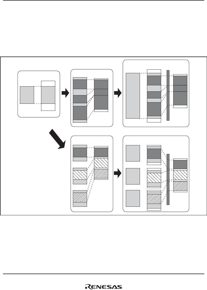
7. Memory Management Unit (MMU)
Rev.1.00 Jan. 10, 2008 Page 145 of 1658
REJ09B0261-0100
There are two methods by which the MMU can perform mapping from virtual memory to physical
memory: the paging method, using fixed-length address translation, and the segment method,
using variable-length address translation. With the paging method, the unit of translation is a
fixed-size address space called a page.
In the following descriptions, the address space in virtual memory in this LSI is referred to as
virtual address space, and the address space in physical memory as physical address space.
MMU
MMU
Process 1
Physical
Memory
(1)
(0)
(2)
(3) (4)
Physical
Memory
Physical
Memory
Physical
Memory
Virtual
Memory
Virtual
Memory
Physical
Memory
Process 1
Process 1
Process 2
Process 3
Process 1
Process 1
Process 2
Process 3
Figure 7.1 Role of MMU
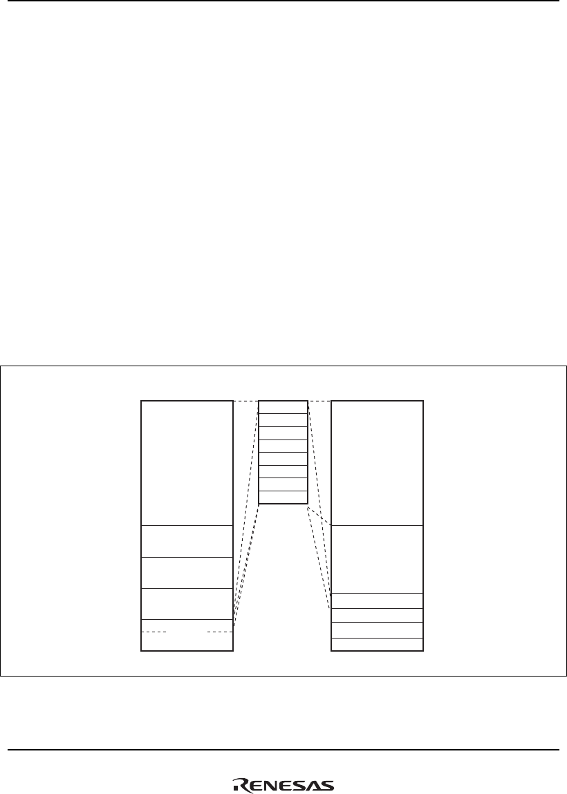
7. Memory Management Unit (MMU)
Rev.1.00 Jan. 10, 2008 Page 146 of 1658
REJ09B0261-0100
7.1.1 Address Spaces
(1) Virtual Address Space
This LSI supports a 32-bit virtual address space, and can access a 4-Gbyte address space. The
virtual address space is divided into a number of areas, as shown in figures 7.2 and 7.3. In
privileged mode, the 4-Gbyte space from the P0 area to the P4 area can be accessed. In user mode,
a 2-Gbyte space in the U0 area can be accessed. When the SQMD bit in the MMU control register
(MMUCR) is 0, a 64-Mbyte space in the store queue area can be accessed. When the RMD bit in
the on-chip memory control register (RAMCR) is 1, a 16-Mbyte space in on-chip memory area
can be accessed. Accessing areas other than the U0 area, store queue area, and on-chip memory
area in user mode will cause an address error.
When the AT bit in MMUCR is set to 1 and the MMU is enabled, the P0, P3, and U0 areas can be
mapped onto any physical address space in 1-, 4-, 64-Kbyte, or 1-Mbyte page units in TLB
compatible mode and in 1-, 4-, 8-, 64-, 256-Kbyte, 1-, 4-, or 64-Mbyte page units in TLB extended
mode. By using an 8-bit address space identifier, the P0, P3, and U0 areas can be increased to a
maximum of 256. Mapping from the virtual address space to the 29-bit physical address space is
carried out using the TLB.
H'0000 0000
H'8000 0000
H'E000 0000
H'E400 0000
H'E500 0000
H'E600 0000
H'FFFF FFFF
H'0000 0000
H'8000 0000
H'FFFF FFFF
H'A000 0000
H'C000 0000
H'E000 0000
Area 0
Area 1
Area 2
Area 3
Area 4
Area 5
Area 6
Area 7
Physical
address space
Address error
Address error
Address error
On-chip memory area
Store queue area
User modePrivileged mode
P1 area
Cacheable
P0 area
Cacheable
P2 area
Non-cacheable
P3 area
Cacheable
P4 area
Non-cacheable
U0 area
Cacheable
Figure 7.2 Virtual Address Space (AT in MMUCR = 0)
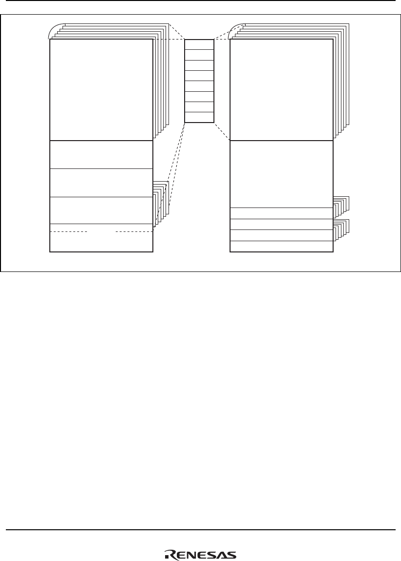
7. Memory Management Unit (MMU)
Rev.1.00 Jan. 10, 2008 Page 147 of 1658
REJ09B0261-0100
Area 0
Area 1
Area 2
Area 3
Area 4
Area 5
Area 6
Area 7
Physical
address space
256
256
U0 area
Cacheable
Address translation possible
Address error
Address error
On-chip memory area
Address error
Store queue area
P0 area
Cacheable
Address translation possible
User mode
Privileged mode
P1 area
Cacheable
Address translation not possible
P2 area
Non-cacheable
Address translation not possible
P3 area
Cacheable
Address translation possible
P4 area
Non-cacheable
Address translation not possible
H'0000 0000
H'8000 0000
H'E000 0000
H'E400 0000
H'E500 0000
H'E600 0000
H'FFFF FFFFH'FFFF FFFF
H'0000 0000
H'8000 0000
H'A000 0000
H'C000 0000
H'E000 0000
Figure 7.3 Virtual Address Space (AT in MMUCR = 1)
(a) P0, P3, and U0 Areas
The P0, P3, and U0 areas allow address translation using the TLB and access using the cache.
When the MMU is disabled, replacing the upper 3 bits of an address with 0s gives the
corresponding physical address. Whether or not the cache is used is determined by the CCR
setting. When the cache is used, switching between the copy-back method and the write-
through method for write accesses is specified by the WT bit in CCR.
When the MMU is enabled, these areas can be mapped onto any physical address space in 1-,
4-, 64-Kbyte, or 1-Mbyte page units in TLB compatible mode and in 1-, 4-, 8-, 64, 256-Kbyte,
1-, 4-, or 64-Mbyte page units in TLB extended mode using the TLB. When CCR is in the
cache enabled state and the C bit for the corresponding page of the TLB entry is 1, accesses
can be performed using the cache. When the cache is used, switching between the copy-back
method and the write-through method for write accesses is specified by the WT bit of the TLB
entry.
When the P0, P3, and U0 areas are mapped onto the control register area which is allocated in
the area 7 in physical address space by means of the TLB, the C bit for the corresponding page
must be cleared to 0.

7. Memory Management Unit (MMU)
Rev.1.00 Jan. 10, 2008 Page 148 of 1658
REJ09B0261-0100
(b) P1 Area
The P1 area does not allow address translation using the TLB but can be accessed using the
cache.
Regardless of whether the MMU is enabled or disabled, clearing the upper 3 bits of an address
to 0 gives the corresponding physical address. Whether or not the cache is used is determined
by the CCR setting. When the cache is used, switching between the copy-back method and the
write-through method for write accesses is specified by the CB bit in CCR.
(c) P2 Area
The P2 area does not allow address translation using the TLB and access using the cache.
Regardless of whether the MMU is enabled or disabled, clearing the upper 3 bits of an address
to 0 gives the corresponding physical address.
(d) P4 Area
The P4 area is mapped onto the internal resource of this LSI. This area except the store queue
and on-chip memory areas does not allow address translation using the TLB. This area cannot
be accessed using the cache. The P4 area is shown in detail in figure 7.4.
H'E000 0000
H'E400 0000
H'F000 0000
H'F100 0000
H'F200 0000
H'F300 0000
H'F400 0000
H'F500 0000
H'F600 0000
H'F700 0000
H'F800 0000
H'FC00 0000
H'FFFF FFFF
Store queue
Reserved area
Reserved area
On-chip memory area
Instruction cache address array
Instruction cache data array
Instruction TLB address array
Instruction TLB data array
Operand cache address array
Operand cache data array
Unified TLB and PMB address array
Unified TLB and PMB data array
Reserved area
Control register area
H'E500 0000
H'E600 0000
Figure 7.4 P4 Area

7. Memory Management Unit (MMU)
Rev.1.00 Jan. 10, 2008 Page 149 of 1658
REJ09B0261-0100
The area from H'E000 0000 to H'E3FF FFFF comprises addresses for accessing the store queues
(SQs). In user mode, the access right is specified by the SQMD bit in MMUCR. For details, see
section 8.7, Store Queues.
The area from H'E500 0000 to H'E5FF FFFF comprises addresses for accessing the on-chip
memory. In user mode, the access right is specified by the RMD bit in RAMCR. For details, see
section 9, On-Chip Memory.
The area from H'F000 0000 to H'F0FF FFFF is used for direct access to the instruction cache
address array. For details, see section 8.6.1, IC Address Array.
The area from H'F100 0000 to H'F1FF FFFF is used for direct access to the instruction cache data
array. For details, see section 8.6.2, IC Data Array.
The area from H'F200 0000 to H'F2FF FFFF is used for direct access to the instruction TLB
address array. For details, see section 7.7.1, ITLB Address Array.
The area from H'F300 0000 to H'F37F FFFF is used for direct access to instruction TLB data
array. For details, see section 7.7.2, ITLB Data Array (TLB Compatible Mode) and section 7.7.3,
ITLB Data Array (TLB Extended Mode).
The area from H'F400 0000 to H'F4FF FFFF is used for direct access to the operand cache address
array. For details, see section 8.6.3, OC Address Array.
The area from H'F500 0000 to H'F5FF FFFF is used for direct access to the operand cache data
array. For details, see section 8.6.4, OC Data Array.
The area from H'F600 0000 to H'F60F FFFF is used for direct access to the unified TLB address
array. For details, see section 7.7.4, UTLB Address Array.
The area from H'F610 0000 to H'F61F FFFF is used for direct access to the PMB address array.
For details, see section 7.8.5, Memory-Mapped PMB Configuration.
The area from H'F700 0000 to H'F70F FFFF is used for direct access to unified TLB data array.
For details, see section 7.7.5, UTLB Data Array (TLB Compatible Mode) and 7.7.6, UTLB Data
Array (TLB Extended Mode).
The area from H'F710 0000 to H'F71F FFFF is used for direct access to the PMB data array. For
details, see section 7.8.5, Memory-Mapped PMB Configuration.
The area from H'FC00 0000 to H'FFFF FFFF is the on-chip peripheral module control register
area. For details, see register descriptions in each section of the hardware manual of the product.

7. Memory Management Unit (MMU)
Rev.1.00 Jan. 10, 2008 Page 150 of 1658
REJ09B0261-0100
(2) Physical Address Space
This LSI supports a 29-bit physical address space. The physical address space is divided into eight
areas as shown in figure 7.5. Area 7 is a reserved area. For details, see section 11, Local Bus State
Controller (LBSC) section of the hardware manual of the product.
Only when area 7 in the physical address space is accessed using the TLB, addresses H'1C00 0000
to H'1FFF FFFF of area 7 are not designated as a reserved area, but are equivalent to the control
register area in the P4 area, in the virtual address space.
H'0000 0000
H'0400 0000
H'0800 0000
H'0C00 0000
H'1000 0000
H'1400 0000
H'1800 0000
H'1C00 0000
H'1FFF FFFF
Area 0
Area 1
Area 2
Area 3
Area 4
Area 5
Area 6
Area 7 (reserved area)
Figure 7.5 Physical Address Space
(3) Address Translation
When the MMU is used, the virtual address space is divided into units called pages, and
translation to physical addresses is carried out in these page units. The address translation table in
external memory contains the physical addresses corresponding to virtual addresses and additional
information such as memory protection codes. Fast address translation is achieved by caching the
contents of the address translation table located in external memory into the TLB. In this LSI,
basically, the ITLB is used for instruction accesses and the UTLB for data accesses. In the event
of an access to an area other than the P4 area, the accessed virtual address is translated to a
physical address. If the virtual address belongs to the P1 or P2 area, the physical address is
uniquely determined without accessing the TLB. If the virtual address belongs to the P0, U0, or P3
area, the TLB is searched using the virtual address, and if the virtual address is recorded in the
TLB, a TLB hit is made and the corresponding physical address is read from the TLB. If the
accessed virtual address is not recorded in the TLB, a TLB miss exception is generated and
processing switches to the TLB miss exception handling routine. In the TLB miss exception
handling routine, the address translation table in external memory is searched, and the
corresponding physical address and page management information are recorded in the TLB. After

7. Memory Management Unit (MMU)
Rev.1.00 Jan. 10, 2008 Page 151 of 1658
REJ09B0261-0100
the return from the exception handling routine, the instruction which caused the TLB miss
exception is re-executed.
(4) Single Virtual Memory Mode and Multiple Virtual Memory Mode
There are two virtual memory systems, single virtual memory and multiple virtual memory, either
of which can be selected with the SV bit in MMUCR. In the single virtual memory system, a
number of processes run simultaneously, using virtual address space on an exclusive basis, and the
physical address corresponding to a particular virtual address is uniquely determined. In the
multiple virtual memory system, a number of processes run while sharing the virtual address
space, and particular virtual addresses may be translated into different physical addresses
depending on the process. The only difference between the single virtual memory and multiple
virtual memory systems in terms of operation is in the TLB address comparison method (see
section 7.3.3, Address Translation Method).
(5) Address Space Identifier (ASID)
In multiple virtual memory mode, an 8-bit address space identifier (ASID) is used to distinguish
between multiple processes running simultaneously while sharing the virtual address space.
Software can set the 8-bit ASID of the currently executing process in PTEH in the MMU. The
TLB does not have to be purged when processes are switched by means of ASID.
In single virtual memory mode, ASID is used to provide memory protection for multiple processes
running simultaneously while using the virtual address space on an exclusive basis.
Note: Two or more entries with the same virtual page number (VPN) but different ASID must
not be set in the TLB simultaneously in single virtual memory mode.

7. Memory Management Unit (MMU)
Rev.1.00 Jan. 10, 2008 Page 152 of 1658
REJ09B0261-0100
7.2 Register Descriptions
The following registers are related to MMU processing.
Table 7.1 Register Configuration
Register Name Abbreviation R/W P4 Address*
Area 7
Address* Size
Page table entry high register PTEH R/W H'FF00 0000 H'1F00 0000 32
Page table entry low register PTEL R/W H'FF00 0004 H'1F00 0004 32
Translation table base register TTB R/W H'FF00 0008 H'1F00 0008 32
TLB exception address register TEA R/W H'FF00 000C H'1F00 000C 32
MMU control register MMUCR R/W H'FF00 0010 H'1F00 0010 32
Page table entry assistance
register
PTEA R/W H'FF00 0034 H'1F00 0034 32
Physical address space control
register
PASCR R/W H'FF00 0070 H'1F00 0070 32
Instruction re-fetch inhibit control
register
IRMCR R/W H'FF00 0078 H'1F00 0078 32
Note: * These P4 addresses are for the P4 area in the virtual address space. These area 7
addresses are accessed from area 7 in the physical address space by means of the
TLB.
Table 7.2 Register States in Each Processing State
Register Name Abbreviation
Power-on
Reset
Manual
Reset Sleep Standby
Page table entry high register PTEH Undefined Undefined Retained Retained
Page table entry low register PTEL Undefined Undefined Retained Retained
Translation table base register TTB Undefined Undefined Retained Retained
TLB exception address register TEA Undefined Retained Retained Retained
MMU control register MMUCR H'0000 0000 H'0000 0000 Retained Retained
Page table entry assistance
register
PTEA H'0000 xxx0 H'0000 xxx0 Retained Retained
Physical address space control
register
PASCR H'0000 0000 H'0000 0000 Retained Retained

7. Memory Management Unit (MMU)
Rev.1.00 Jan. 10, 2008 Page 153 of 1658
REJ09B0261-0100
Register Name Abbreviation
Power-on
Reset
Manual
Reset Sleep Standby
Instruction re-fetch inhibit control
register
IRMCR H'0000 0000 H'0000 0000 Retained Retained
7.2.1 Page Table Entry High Register (PTEH)
PTEH consists of the virtual page number (VPN) and address space identifier (ASID). When an
MMU exception or address error exception occurs, the VPN of the virtual address at which the
exception occurred is set in the VPN bit by hardware. VPN varies according to the page size, but
the VPN set by hardware when an exception occurs consists of the upper 22 bits of the virtual
address which caused the exception. VPN setting can also be carried out by software. The number
of the currently executing process is set in the ASID bit by software. ASID is not updated by
hardware. VPN and ASID are recorded in the UTLB by means of the LDTLB instruction.
After the ASID field in PTEH has been updated, execute one of the following three methods
before an access (including an instruction fetch) to the P0, P3, or U0 area that uses the updated
ASID value is performed.
1. Execute a branch using the RTE instruction. In this case, the branch destination may be the P0,
P3, or U0 area.
2. Execute the ICBI instruction for any address (including non-cacheable area).
3. If the R2 bit in IRMCR is 0 (initial value) before updating the ASID field, the specific
instruction does not need to be executed. However, note that the CPU processing performance
will be lowered because the instruction fetch is performed again for the next instruction after
the ASID field has been updated.
Note that the method 3 may not be guaranteed in the future SuperH Series. Therefore, it is
recommended that the method 1 or 2 should be used for being compatible with the future SuperH
Series.
31 30 29 28 27 26 25 24 23 22 21 20 19 18 17 16
ASIDVPN
VPN
Bit:
Initial value:
R/W:
Bit:
Initial value:
R/W:
1514131211109876543210
00
R/W R/W R/W R/W R/W R/W R R R/W R/W R/W R/W R/W R/W R/W R/W
R/W R/W R/W R/W R/W R/W R/W R/W R/W R/W R/W R/W R/W R/W R/W R/W
7. Memory Management Unit (MMU)
Rev.1.00 Jan. 10, 2008 Page 154 of 1658
REJ09B0261-0100
Bit Bit Name
Initial
Value R/W Description
31 to 10 VPN Undefined R/W Virtual Page Number
9, 8 ⎯ All 0 R Reserved
For details on reading from or writing to these bits, see
description in General Precautions on Handling of
Product.
7 to 0 ASID Undefined R/W Address Space Identifier
7.2.2 Page Table Entry Low Register (PTEL)
PTEL is used to hold the physical page number and page management information to be recorded
in the UTLB by means of the LDTLB instruction. The contents of this register are not changed
unless a software directive is issued.
31 30 29 28 27 26 25 24 23 22 21 20 19 18 17 16
Bit:
000
0
Initial value:
R R R R/W R/W R/W R/W R/W R/W R/W R/W R/W R/W R/W R/W R/W
R/W R/W R/W
PPN
PPN V SZ1 PR1 PR0 SZ0 C D SH WT
R/W R/W R/W R/W R/W
R/W:
Bit:
Initial value:
R/W:
15 14 13 12 11 10 9 8 7 6 5 4 3 2 1 0
R R/W
R/W R/W R/W R/W
R/W R/W
Bit Bit Name
Initial
Value R/W Description
31 to 29 ⎯ All 0 R Reserved
For details on reading from or writing to these bits, see
description in General Precautions on Handling of
Product.
28 to 10 PPN Undefined R/W Physical Page Number
9 ⎯ 0 R Reserved
For details on reading from or writing to this bit, see
description in General Precautions on Handling of
Product.
7. Memory Management Unit (MMU)
Rev.1.00 Jan. 10, 2008 Page 155 of 1658
REJ09B0261-0100
Bit Bit Name
Initial
Value R/W Description
8 V Undefined R/W
7 SZ1 Undefined R/W
6 PR1 Undefined R/W
5 PR0 Undefined R/W
4 SZ0 Undefined R/W
3 C Undefined R/W
2 D Undefined R/W
1 SH Undefined R/W
Page Management Information
The meaning of each bit is same as that of
corresponding bit in Common TLB (UTLB).
For details, see section 7.3, TLB Functions (TLB
Compatible Mode; MMUCR.ME = 0) and section 7.4,
TLB Functions (TLB Extended Mode; MMUCR.ME = 1).
Note: SZ1, PR1, SZ0, and PR0 bits are valid only in
TLB compatible mode.
0 WT Undefined R/W
7.2.3 Translation Table Base Register (TTB)
TTB is used to store the base address of the currently used page table, and so on. The contents of
TTB are not changed unless a software directive is issued. This register can be used freely by
software.
31 30 29 28 27 26 25 24 23 22 21 20 19 18 17 16
Bit:
Initial value:
R/W R/W R/W R/W R/W R/W R/W R/W R/W R/W R/W R/W R/W R/W R/W R/W
R/W R/W R/W
TTB
TTB
R/W R/W R/W R/W R/W
R/W:
Bit:
Initial value:
R/W:
1514131211109876543210
R/WR/W
R/W R/W R/W R/W
R/W R/W

7. Memory Management Unit (MMU)
Rev.1.00 Jan. 10, 2008 Page 156 of 1658
REJ09B0261-0100
7.2.4 TLB Exception Address Register (TEA)
After an MMU exception or address error exception occurs, the virtual address at which the
exception occurred is stored. The contents of this register can be changed by software.
31 30 29 28 27 26 25 24
Virtual address at which MMU exception or address error occurred
Virtual address at which MMU exception or address error occurred
23 22 21 20 19 18 17 16
Bit:
Initial value:
R/W R/W R/W R/W R/W R/W R/W R/W R/W R/W R/W R/W R/W R/W R/W R/W
R/W R/W R/W R/W R/W R/W R/W R/W
R/W:
Bit:
Initial value:
R/W:
1514131211109876543210
R/WR/W
R/W R/W R/W R/W
R/W R/W
TEA
TEA
7.2.5 MMU Control Register (MMUCR)
The individual bits perform MMU settings as shown below. Therefore, MMUCR rewriting should
be performed by a program in the P1 or P2 area.
After MMUCR has been updated, execute one of the following three methods before an access
(including an instruction fetch) to the P0, P3, U0, or store queue area is performed.
1. Execute a branch using the RTE instruction. In this case, the branch destination may be the P0,
P3, or U0 area.
2. Execute the ICBI instruction for any address (including non-cacheable area).
3. If the R2 bit in IRMCR is 0 (initial value) before updating MMUCR, the specific instruction
does not need to be executed. However, note that the CPU processing performance will be
lowered because the instruction fetch is performed again for the next instruction after
MMUCR has been updated.
Note that the method 3 may not be guaranteed in the future SuperH Series. Therefore, it is
recommended that the method 1 or 2 should be used for being compatible with the future SuperH
Series.
MMUCR contents can be changed by software. However, the LRUI and URC bits may also be
updated by hardware.

7. Memory Management Unit (MMU)
Rev.1.00 Jan. 10, 2008 Page 157 of 1658
REJ09B0261-0100
31 30 29 28 27 26 25 24 23 22 21 20 19 18 17 16
Bit:
0000000000000000
Initial value:
R/W R/W R/W R/W R/W R/W R R R/W R/W R/W R/W R/W R/W R R
R/W R R
TI
URBLRUI
URC SQMD SV AT
R R R/W R R/W
R/W:
Bit:
Initial value:
R/W:
15 14 13 12 11 10 9 8 7 6 5 4 3 2 1 0
0000000000000000
R/W R/W R/W R/W R/W R/W R/W R/W
ME
Bit Bit Name
Initial
Value R/W Description
31 to 26 LRUI 000000 R/W Least Recently Used ITLB
These bits indicate the ITLB entry to be replaced. The
LRU (least recently used) method is used to decide the
ITLB entry to be replaced in the event of an ITLB miss.
The entry to be purged from the ITLB can be confirmed
using the LRUI bits.
LRUI is updated by means of the algorithm shown below.
x means that updating is not performed.
000xxx: ITLB entry 0 is used
1xx00x: ITLB entry 1 is used
x1x1x0: ITLB entry 2 is used
xx1x11: ITLB entry 3 is used
xxxxxx: Other than above
When the LRUI bit settings are as shown below, the
corresponding ITLB entry is updated by an ITLB miss.
Ensure that values for which "Setting prohibited" is
indicated below are not set at the discretion of software.
After a power-on or manual reset, the LRUI bits are
initialized to 0, and therefore a prohibited setting is never
made by a hardware update.
x means "don't care".
111xxx: ITLB entry 0 is updated
0xx11x: ITLB entry 1 is updated
x0x0x1: ITLB entry 2 is updated
xx0x00: ITLB entry 3 is updated
Other than above: Setting prohibited

7. Memory Management Unit (MMU)
Rev.1.00 Jan. 10, 2008 Page 158 of 1658
REJ09B0261-0100
Bit Bit Name
Initial
Value R/W Description
25, 24 ⎯ All 0 R Reserved
For details on reading from or writing to these bits, see
description in General Precautions on Handling of
Product.
23 to 18 URB 000000 R/W UTLB Replace Boundary
These bits indicate the UTLB entry boundary at which
replacement is to be performed. Valid only when URB ≠
0.
17, 16 ⎯ All 0 R Reserved
For details on reading from or writing to these bits, see
description in General Precautions on Handling of
Product.
15 to 10 URC 000000 R/W UTLB Replace Counter
These bits serve as a random counter for indicating the
UTLB entry for which replacement is to be performed
with an LDTLB instruction. This bit is incremented each
time the UTLB is accessed. If URB > 0, URC is cleared
to 0 when the condition URC = URB is satisfied. Also
note that if a value is written to URC by software which
results in the condition of URC > URB, incrementing is
first performed in excess of URB until URC = H'3F.
URC is not incremented by an LDTLB instruction.
9 SQMD 0 R/W Store Queue Mode
Specifies the right of access to the store queues.
0: User/privileged access possible
1: Privileged access possible (address error exception
in case of user access)
8 SV 0 R/W Single Virtual Memory Mode/Multiple Virtual Memory
Mode Switching
When this bit is changed, ensure that 1 is also written
to the TI bit.
0: Multiple virtual memory mode
1: Single virtual memory mode

7. Memory Management Unit (MMU)
Rev.1.00 Jan. 10, 2008 Page 159 of 1658
REJ09B0261-0100
Bit Bit Name
Initial
Value R/W Description
7 ME 0 R/W TLB Extended Mode Switching
0: TLB compatible mode
1: TLB extended mode
For modifying the ME bit value, always set the TI bit to
1 to invalidate the contents of ITLB and UTLB. The
selection of TLB operating mode made by the ME bit
does not affect the functionality or operation of the
PMB.
6 to 3 ⎯ All 0 R Reserved
For details on reading from or writing to these bits, see
description in General Precautions on Handling of
Product.
2 TI 0 R/W TLB Invalidate Bit
Writing 1 to this bit invalidates (clears to 0) all valid
UTLB/ITLB bits. This bit is always read as 0.
1 ⎯ 0 R Reserved
For details on reading from or writing to this bit, see
description in General Precautions on Handling of
Product.
0 AT 0 R/W Address Translation Enable Bit
These bits enable or disable the MMU.
0: MMU disabled
1: MMU enabled
MMU exceptions are not generated when the AT bit is
0. In the case of software that does not use the MMU,
the AT bit should be cleared to 0.
7.2.6 Page Table Entry Assistance Register (PTEA)
31 30 29 28 27 26 25 24 23 22 21 20 19 18 17 16
15 14 13 12 11 10 9 8 7 6 5 4 3 2 1 0
0000000000000000
RRRRRRRRRRRRRRRR
00−−−−−−−−−−0000
R R R/W R/W R/W R/W R/W R/W R/W R/W R/W R/W R R R R
Bit:
Initial value:
R/W:
Bit:
Initial value:
R/W:
−−−−−−−−−−−−−−−−
−− EPR ESZ −−−−
7. Memory Management Unit (MMU)
Rev.1.00 Jan. 10, 2008 Page 160 of 1658
REJ09B0261-0100
Bit Bit Name
Initial
Value R/W Description
31 to 14 ⎯ All 0 R Reserved
For details on reading/writing these bits, see General
Precautions on Handling of Product.
13 to 8 EPR Undefined R/W
7 to 4 ESZ Undefined R/W
Page Control Information
Each bit has the same function as the corresponding
bit of the unified TLB (UTLB). For details, see section
7.4, TLB Functions (TLB Extended Mode; MMUCR.ME
= 1)
3 to 0 ⎯ All 0 R Reserved
For details on reading/writing these bits, see General
Precautions on Handling of Product.
7.2.7 Physical Address Space Control Register (PASCR)
PASCR controls the operation in the physical address space.
31 30 29 28 27 26 25 24 23 22 21 20 19 18 17 16
Bit:
00000000
000000
00000000
Initial value:
RRRRRRRRRRRRRRRR
R/W
UB
R/W R/W R/W R/W R/W R/W R/W
R/W:
Bit:
Initial value:
R/W:
1514131211109876543210
00 000000
00
RRRRRRRR

7. Memory Management Unit (MMU)
Rev.1.00 Jan. 10, 2008 Page 161 of 1658
REJ09B0261-0100
Bit Bit Name
Initial
Value R/W Description
31 to 8 ⎯ All 0 R Reserved
For details on reading from or writing to these bits, see
description in General Precautions on Handling of
Product.
7 to 0 UB H'00 R/W Buffered Write Control for Each Area (64 Mbytes)
When writing is performed without using the cache or in
the cache write-through mode, these bits specify
whether the next bus access from the CPU waits for the
end of writing for each area.
0 : Buffered write (The CPU does not wait for the end of
writing bus access and starts the next bus access)
1 : Unbuffered write (The CPU waits for the end of
writing bus access and starts the next bus access)
UB[7]: Corresponding to the control register area
UB[6]: Corresponding to area 6
UB[5]: Corresponding to area 5
UB[4]: Corresponding to area 4
UB[3]: Corresponding to area 3
UB[2]: Corresponding to area 2
UB[1]: Corresponding to area 1
UB[0]: Corresponding to area 0

7. Memory Management Unit (MMU)
Rev.1.00 Jan. 10, 2008 Page 162 of 1658
REJ09B0261-0100
7.2.8 Instruction Re-Fetch Inhibit Control Register (IRMCR)
When the specific resource is changed, IRMCR controls whether the instruction fetch is
performed again for the next instruction. The specific resource means the part of control registers,
TLB, and cache.
In the initial state, the instruction fetch is performed again for the next instruction after changing
the resource. However, the CPU processing performance will be lowered because the instruction
fetch is performed again for the next instruction every time the resource is changed. Therefore, it
is recommended that each bit in IRMCR is set to 1 and the specific instruction should be executed
after all necessary resources have been changed prior to execution of the program which uses
changed resources.
For details on the specific sequence, see descriptions in each resource.
31 30 29 28 27 26 25 24 23 22 21 20 19 18 17 16
Bit:
00000000
000000
00000000
Initial value:
RRRRRRRRRRRRRRRR
R
R2 R1 LT MT MC
R R R/W R/W R/W R/W R/W
R/W:
Bit:
Initial value:
R/W:
1514131211109876543210
00 000000
00
RRRRRRRR
Bit Bit Name
Initial
Value R/W Description
31 to 5 ⎯ All 0 R Reserved
For details on reading from or writing to these bits, see
description in General Precautions on Handling of
Product.
4 R2 0 R/W Re-Fetch Inhibit 2 after Register Change
When MMUCR, PASCR, CCR, PTEH, or RAMCR is
changed, this bit controls whether re-fetch is performed
for the next instruction.
0: Re-fetch is performed
1: Re-fetch is not performed

7. Memory Management Unit (MMU)
Rev.1.00 Jan. 10, 2008 Page 163 of 1658
REJ09B0261-0100
Bit Bit Name
Initial
Value R/W Description
3 R1 0 R/W Re-Fetch Inhibit 1 after Register Change
When a register allocated in addresses H'FF200000 to
H'FF2FFFFF is changed, this bit controls whether re-
fetch is performed for the next instruction.
0: Re-fetch is performed
1: Re-fetch is not performed
2 LT 0 R/W Re-Fetch Inhibit after LDTLB Execution
This bit controls whether re-fetch is performed for the
next instruction after the LDTLB instruction has been
executed.
0: Re-fetch is performed
1: Re-fetch is not performed
1 MT 0 R/W Re-Fetch Inhibit after Writing Memory-Mapped TLB
This bit controls whether re-fetch is performed for the
next instruction after writing memory-mapped
ITLB/UTLB while the AT bit in MMUCR is set to 1.
0: Re-fetch is performed
1: Re-fetch is not performed
0 MC 0 R/W Re-Fetch Inhibit after Writing Memory-Mapped IC
This bit controls whether re-fetch is performed for the
next instruction after writing memory-mapped IC while
the ICE bit in CCR is set to 1.
0: Re-fetch is performed
1: Re-fetch is not performed
7. Memory Management Unit (MMU)
Rev.1.00 Jan. 10, 2008 Page 164 of 1658
REJ09B0261-0100
7.3 TLB Functions (TLB Compatible Mode; MMUCR.ME = 0)
7.3.1 Unified TLB (UTLB) Configuration
The UTLB is used for the following two purposes:
1. To translate a virtual address to a physical address in a data access
2. As a table of address translation information to be recorded in the ITLB in the event of an
ITLB miss
The UTLB is so called because of its use for the above two purposes. Information in the address
translation table located in external memory is cached into the UTLB. The address translation
table contains virtual page numbers and address space identifiers, and corresponding physical page
numbers and page management information. Figure 7.6 shows the UTLB configuration. The
UTLB consists of 64 fully-associative type entries. Figure 7.7 shows the relationship between the
page size and address format.
PPN[28:10]
PPN[28:10]
PPN[28:10]
SZ[1:0]
SZ[1:0]
SZ[1:0]
SH
SH
SH
C
C
C
PR[1:0]
PR[1:0]
PR [1:0]
ASID[7:0]
ASID[7:0]
ASID[7:0]
VPN[31:10]
VPN[31:10]
VPN[31:10]
V
V
V
Entry 0
Entry 1
Entry 2
D
D
D
WT
WT
WT
PPN[28:10] SZ[1:0] SH C PR[1:0]ASID[7:0] VPN[31:10] VEntry 63 D WT
Figure 7.6 UTLB Configuration (TLB Compatible Mode)
Legend:
• VPN: Virtual page number
For 1-Kbyte page: Upper 22 bits of virtual address
For 4-Kbyte page: Upper 20 bits of virtual address
For 64-Kbyte page: Upper 16 bits of virtual address
For 1-Mbyte page: Upper 12 bits of virtual address
• ASID: Address space identifier
Indicates the process that can access a virtual page.
In single virtual memory mode and user mode, or in multiple virtual memory mode, if the SH
bit is 0, this identifier is compared with the ASID in PTEH when address comparison is
performed.

7. Memory Management Unit (MMU)
Rev.1.00 Jan. 10, 2008 Page 165 of 1658
REJ09B0261-0100
• SH: Share status bit
When 0, pages are not shared by processes.
When 1, pages are shared by processes.
• SZ[1:0]: Page size bits
Specify the page size.
00: 1-Kbyte page
01: 4-Kbyte page
10: 64-Kbyte page
11: 1-Mbyte page
• V: Validity bit
Indicates whether the entry is valid.
0: Invalid
1: Valid
Cleared to 0 by a power-on reset.
Not affected by a manual reset.
• PPN: Physical page number
Upper 22 bits of the physical address of the physical page number.
With a 1-Kbyte page, PPN[28:10] are valid.
With a 4-Kbyte page, PPN[28:12] are valid.
With a 64-Kbyte page, PPN[28:16] are valid.
With a 1-Mbyte page, PPN[28:20] are valid.
The synonym problem must be taken into account when setting the PPN (see section 7.5.5,
Avoiding Synonym Problems).
• PR[1:0]: Protection key data
2-bit data expressing the page access right as a code.
00: Can be read from only in privileged mode
01: Can be read from and written to in privileged mode
10: Can be read from only in privileged or user mode
11: Can be read from and written to in privileged mode or user mode
• C: Cacheability bit
Indicates whether a page is cacheable.
0: Not cacheable
7. Memory Management Unit (MMU)
Rev.1.00 Jan. 10, 2008 Page 166 of 1658
REJ09B0261-0100
1: Cacheable
When the control register area is mapped, this bit must be cleared to 0.
• D: Dirty bit
Indicates whether a write has been performed to a page.
0: Write has not been performed
1: Write has been performed
• WT: Write-through bit
Specifies the cache write mode.
0: Copy-back mode
1: Write-through mode
31
• 1-Kbyte page
10 9 0
Virtual address
31
• 4-Kbyte page
12 11 0
Virtual address
31
• 64-Kbyte page
16 15 0
Virtual address
31
• 1-Mbyte page
20 19 0
Virtual address
VPN
Offset
VPN Offset
VPN Offset
VPN Offset
28 10 9 0
Physical address
28 12 11 0
Physical address
28 16 15 0
Physical address
28 20 19 0
Physical address
PPN Offset
PPN Offset
PPN Offset
PPN Offset
Figure 7.7 Relationship between Page Size and Address Format (TLB Compatible Mode)
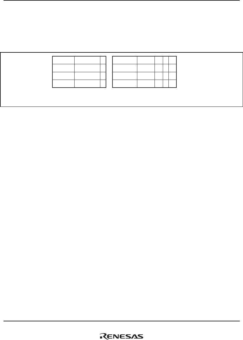
7. Memory Management Unit (MMU)
Rev.1.00 Jan. 10, 2008 Page 167 of 1658
REJ09B0261-0100
7.3.2 Instruction TLB (ITLB) Configuration
The ITLB is used to translate a virtual address to a physical address in an instruction access.
Information in the address translation table located in the UTLB is cached into the ITLB. Figure
7.8 shows the ITLB configuration. The ITLB consists of four fully-associative type entries.
PPN[28:10]
PPN[28:10]
PPN[28:10]
PPN[28:10]
SZ[1:0]
SZ[1:0]
SZ[1:0]
SZ[1:0]
SH
SH
SH
SH
C
C
C
C
PR
PR
PR
PR
ASID[7:0]
ASID[7:0]
ASID[7:0]
ASID[7:0]
VPN[31:10]
VPN[31:10]
VPN[31:10]
VPN[31:10]
V
V
V
V
Entry 0
Entry 1
Entry 2
Entry 3
Notes: 1. The D and WT bits are not supported.
2. There is only one PR bit, corresponding to the upper bit of the PR bits in the UTLB.
Figure 7.8 ITLB Configuration (TLB Compatible Mode)
7.3.3 Address Translation Method
Figure 7.9 shows a flowchart of a memory access using the UTLB.
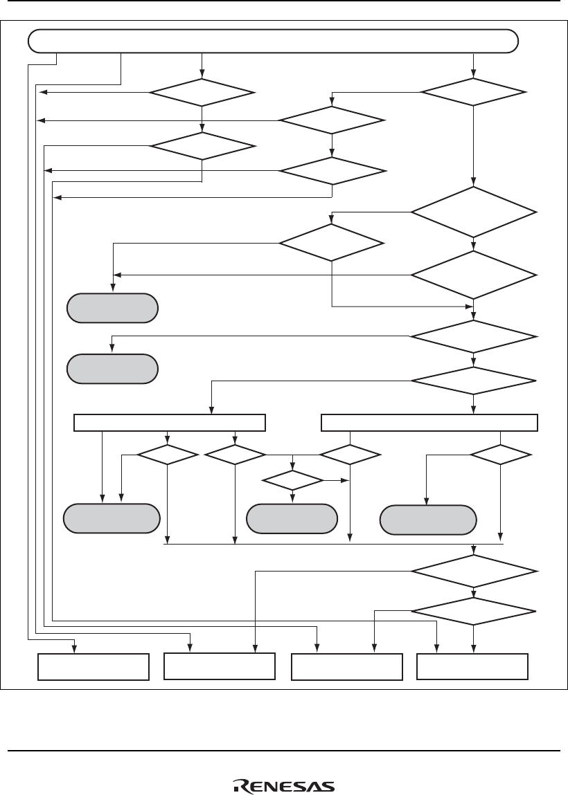
7. Memory Management Unit (MMU)
Rev.1.00 Jan. 10, 2008 Page 168 of 1658
REJ09B0261-0100
SR.MD?
R/W?
R/W?
Yes
Yes
No
No
No
Yes
Yes
Yes
No
PR? PR?
D?
R/W? WW
W
RRR R
W
R/W?
WT?
1
1
0
0
00 or
01
10 11 01 or 11 00 or 10
Yes
No
Internal resource access
1
0CCR.OCE?
1
0
CCR.CB?
0
1
CCR.WT?
1
0CCR.OCE?
No
Data access to virtual address (VA)
VA is
in P4 area
VA is
in P2 area
VA is
in P1 area
VA is in P0, U0,
or P3 area
MMUCR.AT = 1
SH = 0
and (MMUCR.SV = 0 or
SR.MD = 0)
VPNs match,
ASIDs match, and
V = 1
Only one
entry matches
1 (Privileged)
Data TLB multiple
hit exception
Data TLB protection
violation exception
Data TLB miss
exception
0 (User)
VPNs match
and V = 1
Data TLB protection
violation exception
Initial page write
exception
Cache access
in copy-back mode
Cache access
in write-through mode
Memory access
(Non-cacheable)
C = 1 and
CCR.OCE = 1
Figure 7.9 Flowchart of Memory Access Using UTLB (TLB Compatible Mode)
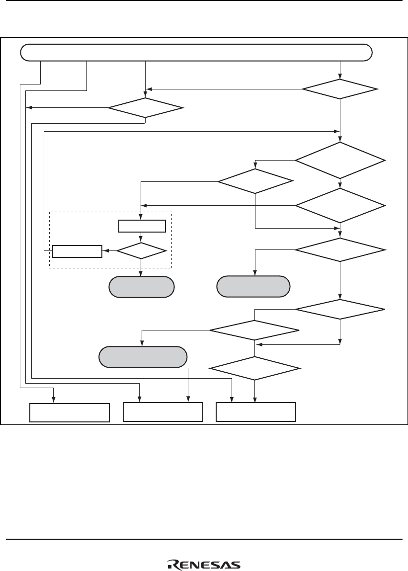
7. Memory Management Unit (MMU)
Rev.1.00 Jan. 10, 2008 Page 169 of 1658
REJ09B0261-0100
Figure 7.10 shows a flowchart of a memory access using the ITLB.
Yes
Yes
No
No
No
Yes
Yes
Yes
No
Internal resource access
1
0
1
0CCR.ICE?
Yes
No
No
Yes
No
Instruction access to virtual address (VA)
VA is
in P4 area VA is
in P2 area
VA is
in P1 area
VA is in P0, U0,
or P3 area
MMUCR.AT = 1
SH = 0
and (MMUCR.SV = 0 or
SR.MD = 0)
VPNs match
and V = 1
VPNs match,
ASIDs match, and
V = 1
Only one
entry matches
SR.MD?
Instruction TLB
multiple hit exception
0 (User)
1 (Privileged)
PR?
C = 1
and CCR.ICE = 1
Cache access
Memory access
(Non-cacheable)
Instruction TLB protection
violation exception
Instruction TLB
miss exception
Hardware ITLB
miss handlingSearch UTLB
Match?
Record in ITLB
Figure 7.10 Flowchart of Memory Access Using ITLB (TLB Compatible Mode)
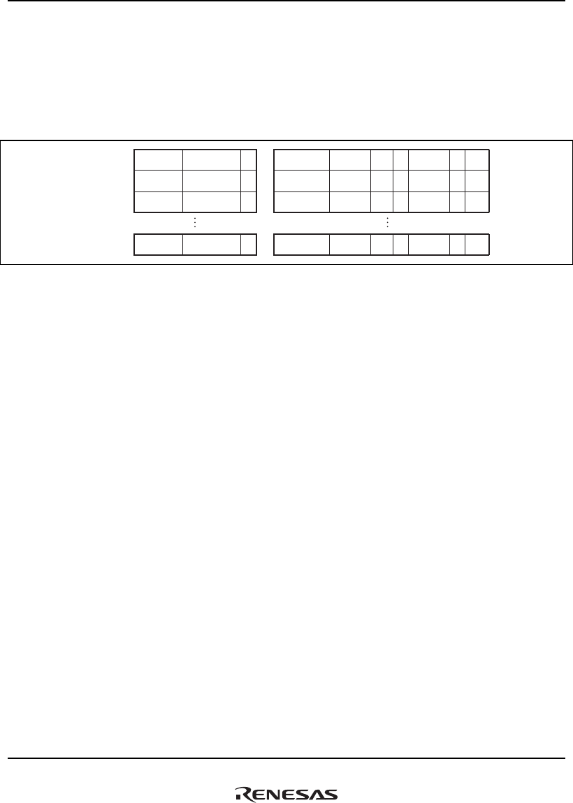
7. Memory Management Unit (MMU)
Rev.1.00 Jan. 10, 2008 Page 170 of 1658
REJ09B0261-0100
7.4 TLB Functions (TLB Extended Mode; MMUCR.ME = 1)
7.4.1 Unified TLB (UTLB) Configuration
Figure 7.11 shows the configuration of the UTLB in TLB extended mode. Figure 7.12 shows the
relationship between the page size and address format.
PPN[28:10]
PPN[28:10]
PPN[28:10]
ESZ[3:0]
ESZ[3:0]
ESZ[3:0]
SH
SH
SH
C
C
C
EPR[5:0]
EPR[5:0]
EPR[5:0]
ASID[7:0]
ASID[7:0]
ASID[7:0]
VPN[31:10]
VPN[31:10]
VPN[31:10]
V
V
V
Entry 0
Entry 1
Entry 2
D
D
D
WT
WT
WT
PPN[28:10]
ESZ[3:0]
SH C
EPR[5:0]
ASID[7:0]
VPN[31:10] VEntry 63 DWT
Figure 7.11 UTLB Configuration (TLB Extended Mode)
Legend:
• VPN: Virtual page number
For 1-Kbyte page: Upper 22 bits of virtual address
For 4-Kbyte page: Upper 20 bits of virtual address
For 8-Kbyte page: Upper 19 bits of virtual address
For 64-Kbyte page: Upper 16 bits of virtual address
For 256-Kbyte page: Upper 14 bits of virtual address
For 1-Mbyte page: Upper 12 bits of virtual address
For 4-Mbyte page: Upper 10 bits of virtual address
For 64-Mbyte page: Upper 6 bits of virtual address
• ASID: Address space identifier
Indicates the process that can access a virtual page.
In single virtual memory mode and user mode, or in multiple virtual memory mode, if the SH
bit is 0, this identifier is compared with the ASID in PTEH when address comparison is
performed.
• SH: Share status bit
When 0, pages are not shared by processes.
When 1, pages are shared by processes.
• ESZ: Page size bits
Specify the page size.
0000: 1-Kbyte page

7. Memory Management Unit (MMU)
Rev.1.00 Jan. 10, 2008 Page 171 of 1658
REJ09B0261-0100
0001: 4-Kbyte page
0010: 8-Kbyte page
0100: 64-Kbyte page
0101: 256-Kbyte page
0111: 1-Mbyte page
1000: 4-Mbyte page
1100: 64-Mbyte page
Note: When a value other than those listed above is recorded, operation is not guaranteed.
• V: Validity bit
Indicates whether the entry is valid.
0: Invalid
1: Valid
Cleared to 0 by a power-on reset.
Not affected by a manual reset.
• PPN: Physical page number
Upper 19 bits of the physical address.
With a 1-Kbyte page, PPN[28:10] are valid.
With a 4-Kbyte page, PPN[28:12] are valid.
With a 8-Kbyte page, PPN[28:13] are valid.
With a 64-Kbyte page, PPN[28:16] are valid.
With a 256-Kbyte page, PPN[28:18] are valid.
With a 1-Mbyte page, PPN[28:20] are valid.
With a 4-Mbyte page, PPN[28:22] are valid.
With a 64-Mbyte page, PPN[28:26] are valid.
The synonym problem must be taken into account when setting the PPN (see section 7.5.5,
Avoiding Synonym Problems).
• EPR: Protection key data
6-bit data expressing the page access right as a code.
Reading, writing, and execution (instruction fetch) in privileged mode and reading, writing,
and execution (instruction fetch) in user mode can be set independently. Each bit is disabled by
0 and enabled by 1.
EPR[5]: Reading in privileged mode
EPR[4]: Writing in privileged mode
EPR[3]: Execution in privileged mode (instruction fetch)
EPR[2]: Reading in user mode

7. Memory Management Unit (MMU)
Rev.1.00 Jan. 10, 2008 Page 172 of 1658
REJ09B0261-0100
EPR[1]: Writing in user mode
EPR[0]: Execution in user mode (instruction fetch)
• C: Cacheability bit
Indicates whether a page is cacheable.
0: Not cacheable
1: Cacheable
When the control register area is mapped, this bit must be cleared to 0.
• D: Dirty bit
Indicates whether a write has been performed to a page.
0: Write has not been performed.
1: Write has been performed.
• WT: Write-through bit
Specifies the cache write mode.
0: Copy-back mode
1: Write-through mode
7. Memory Management Unit (MMU)
Rev.1.00 Jan. 10, 2008 Page 173 of 1658
REJ09B0261-0100
Virtual address Physical address
31
1-Kbyte page
10 9 0
VPN Offset
28 10 9 0
PPN Offset
31
4-Kbyte page
12 11 0
VPN Offset
28 12 11 0
PPN Offset
31
64-Kbyte page
16 15 0
VPN Offset
28 16 15 0
PPN Offset
31
8-Kbyte page
13 12 0
VPN Offset
28 13 12 0
PPN Offset
31
1-Mbyte page
20 19 0
VPN Offset
28 20 19 0
PPN Offset
31
4-Mbyte page
22 21 0
VPN Offset
28 22 21 0
PPN Offset
31
64-Mbyte page
26 25 0
VPN Offset
28 26 25 0
PPN Offset
31
256-Kbyte page
18 17 0
VPN Offset
28 18 17 0
PPN Offset
Figure 7.12 Relationship between Page Size and Address Format (TLB Extended Mode)
7.4.2 Instruction TLB (ITLB) Configuration
Figure 7.13 shows the configuration of the ITLB in TLB extended mode.
PPN[28:10]
PPN[28:10]
PPN[28:10]
PPN[28:10]
ESZ[3:0]
ESZ[3:0]
ESZ[3:0]
ESZ[3:0]
SH
SH
SH
SH
C
C
C
C
EPR[5]
EPR[5]
EPR[5]
EPR[5]
EPR[3]
EPR[3]
EPR[3]
EPR[3]
EPR[2]
EPR[2]
EPR[2]
EPR[2]
EPR[0]
EPR[0]
EPR[0]
EPR[0]
ASID[7:0]
ASID[7:0]
ASID[7:0]
ASID[7:0]
VPN[31:10]
VPN[31:10]
VPN[31:10]
VPN[31:10]
V
V
V
V
Entry 0
Entry 1
Entry 2
Entry 3
Note: Bits EPR[4], EPR[1],
D, and WT are not supported.
Figure 7.13 ITLB Configuration (TLB Extended Mode)

7. Memory Management Unit (MMU)
Rev.1.00 Jan. 10, 2008 Page 174 of 1658
REJ09B0261-0100
7.4.3 Address Translation Method
Figure 7.14 is a flowchart of memory access using the UTLB in TLB extended mode.
7. Memory Management Unit (MMU)
Rev.1.00 Jan. 10, 2008 Page 175 of 1658
REJ09B0261-0100
SH = 0
and (MMUCR.SV = 0 or
SR.MD = 0)
VPNs match,
ASIDs match, and
V = 1
Only one
entry matches
SR.MD?
Cache access
in write-through mode
Data TLB protection
violation exception
Initial page write
exception
Data TLB protection
violation exception
Cache access
in copy-back mode
EPR[5]?
EPR[4]?
Data access to virtual address (VA)
VA is
in P4 area
VA is
in P2 area
VA is
in P1 area
VA is in P0, U0,
or P3 area
Yes
Yes
No
No
No
Yes
Yes
Yes
No
1 (Privileged)
R/W? R/W?
0 (User)
D?
EPR[1]?
00
11
0
11
0
EPR[2]?
WT?
C = 1 and
CCR.OCE = 1
0
1
1
0
RWW
R
MMUCR.AT = 1
Yes
No
Data TLB multiple
hit exception
Data TLB miss
exception
Memory access
(Non-cacheable)
Internal resource access
1
0CCR.OCE?
1
0
CCR.CB?
0
1
CCR.WT?
VPNs match
and V = 1
1
0CCR.OCE?
No
Figure 7.14 Flowchart of Memory Access Using UTLB (TLB Extended Mode)
7. Memory Management Unit (MMU)
Rev.1.00 Jan. 10, 2008 Page 176 of 1658
REJ09B0261-0100
Figure 7.15 is a flowchart of memory access using the ITLB in TLB extended mode.
SH = 0
and (MMUCR.SV = 0 or
SR.MD = 0)
VPNs match,
ASIDs match, and
V = 1
Only one
entry matches
SR.MD?
Instruction TLB protection
violation exception
Instruction TLB
multiple hit exception
Instruction access to virtual address (VA)
VA is
in P4 area
VA is
in P2 area VA is
in P1 area
VA is in P0, U0,
or P3 area
Yes
Yes
No
No
No
Yes
Yes
1 (Privileged)
Search UTLB
0 (User)
Hardware ITLB
miss handling
Match?
MMUCR.AT = 1
Yes
No
Instruction TLB
miss exception
Memory access
(Non-cacheable)
Internal resource access
VPNs match
and V = 1
1
0CCR.ICE?
Yes
No
C = 1 and
CCR.ICE = 1
EPR[2] = 0 and
EPR[0] = 0
EPR[0]?
No
Record in ITLB
Yes
No
Yes
No
Yes
11
00
No
ICBI or normal instruction access?
ICBI Normal instruction access ICBI Normal instruction access
ICBI or normal instruction access?
EPR[5] = 0 and
EPR[3] = 0
EPR[3]?
Cache access
Figure 7.15 Flowchart of Memory Access Using ITLB (TLB Extended Mode)

7. Memory Management Unit (MMU)
Rev.1.00 Jan. 10, 2008 Page 177 of 1658
REJ09B0261-0100
7.5 MMU Functions
7.5.1 MMU Hardware Management
This LSI supports the following MMU functions.
1. The MMU decodes the virtual address to be accessed by software, and performs address
translation by controlling the UTLB/ITLB in accordance with the MMUCR settings.
2. The MMU determines the cache access status on the basis of the page management
information read during address translation (C and WT bits).
3. If address translation cannot be performed normally in a data access or instruction access, the
MMU notifies software by means of an MMU exception.
4. If address translation information is not recorded in the ITLB in an instruction access, the
MMU searches the UTLB. If the necessary address translation information is recorded in the
UTLB, the MMU copies this information into the ITLB in accordance with the LRUI bit
setting in MMUCR.
7.5.2 MMU Software Management
Software processing for the MMU consists of the following:
1. Setting of MMU-related registers. Some registers are also partially updated by hardware
automatically.
2. Recording, deletion, and reading of TLB entries. There are two methods of recording UTLB
entries: by using the LDTLB instruction, or by writing directly to the memory-mapped UTLB.
ITLB entries can only be recorded by writing directly to the memory-mapped ITLB. Deleting
or reading UTLB/ITLB entries is enabled by accessing the memory-mapped UTLB/ITLB.
3. MMU exception handling. When an MMU exception occurs, processing is performed based on
information set by hardware.

7. Memory Management Unit (MMU)
Rev.1.00 Jan. 10, 2008 Page 178 of 1658
REJ09B0261-0100
7.5.3 MMU Instruction (LDTLB)
A TLB load instruction (LDTLB) is provided for recording UTLB entries. When an LDTLB
instruction is issued, this LSI copies the contents of PTEH and PTEL (also the contents of PTEA
in TLB extended mode) to the UTLB entry indicated by the URC bit in MMUCR. ITLB entries
are not updated by the LDTLB instruction, and therefore address translation information purged
from the UTLB entry may still remain in the ITLB entry. As the LDTLB instruction changes
address translation information, ensure that it is issued by a program in the P1 or P2 area.
After the LDTLB instruction has been executed, execute one of the following three methods
before an access (include an instruction fetch) the area where TLB is used to translate the address
is performed.
1. Execute a branch using the RTE instruction. In this case, the branch destination may be the
area where TLB is used to translate the address.
2. Execute the ICBI instruction for any address (including non-cacheable area).
3. If the LT bit in IRMCR is 0 (initial value) before executing the LDTLB instruction, the
specific instruction does not need to be executed. However, note that the CPU processing
performance will be lowered because the instruction fetch is performed again for the next
instruction after MMUCR has been updated.
Note that the method 3 may not be guaranteed in the future SuperH Series. Therefore, it is
recommended that the method 1 or 2 should be used for being compatible with the future SuperH
Series.
7. Memory Management Unit (MMU)
Rev.1.00 Jan. 10, 2008 Page 179 of 1658
REJ09B0261-0100
The operation of the LDTLB instruction is shown in figures 7.16 and 7.17.
PPN [28:10]
PPN [28:10]
PPN [28:10]
SZ [1:0]
SZ [1:0]
SZ [1:0]
SH
SH
SH
C
C
C
PR [1:0]
PR [1:0]
PR [1:0]
ASID [7:0]
ASID [7:0]
ASID [7:0]
VPN [31:10]
VPN [31:10]
VPN [31:10]
V
V
V
Entry 0
Entry 1
Entry 2
D
D
D
WT
WT
WT
PPN [28:10] SZ [1:0] SH C PR [1:0]ASID [7:0] VPN [31:10] VEntry 63 D WT
31 2928 9 8 765 4 3 2 1 0
——
V
SZ1 PR[1:0] SZ0
CDSH
WT
PTEL
Write
UTLB
31 10 9 87 0
— ASID
PTEH
31 26252423 18171615 10 9 87 3 2 1 0
LRUI — URB — URC SV — TI — AT
MMUCR
VPN
10
PPN
Entry specification SQMD
Figure 7.16 Operation of LDTLB Instruction (TLB Compatible Mode)
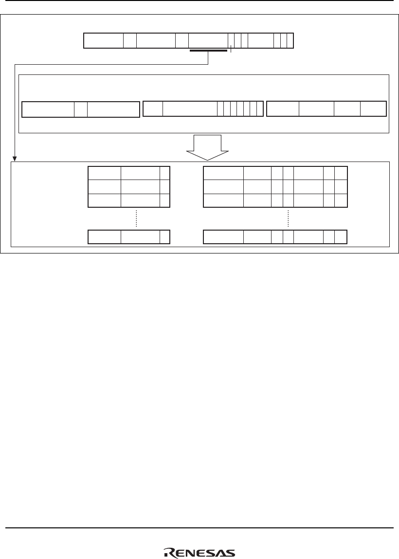
7. Memory Management Unit (MMU)
Rev.1.00 Jan. 10, 2008 Page 180 of 1658
REJ09B0261-0100
PPN[28:10]
PPN[28:10]
PPN[28:10]
ESZ
[
3:0
]
ESZ
[
3:0
]
ESZ
[
3:0
]
SH
SH
SH
C
C
C
EPR
[
5:0
]
EPR
[
5:0
]
EPR
[
5:0
]
ASID[7:0]
ASID[7:0]
ASID[7:0]
VPN
[
31:10
]
VPN
[
31:10
]
VPN
[
31:10
]
V
V
V
Entry 0
Entry 1
Entry 2
D
D
D
WT
WT
WT
PPN[28:10]
ESZ
[
3:0]
SH C
EPR
[
5:0]
ASID[7:0]
VPN
[
31:10
]
VEntry 63 D WT
−−−
VCD
SH
WT
Write
−ASID
PTEH PTEL
LRUI −URB −URC
SV ME
−−TI AT
MMUCR
VPN PPN −
PTEA
EPR ESZ −
Entry specification
SQMD
Figure 7.17 Operation of LDTLB Instruction (TLB Extended Mode)
7.5.4 Hardware ITLB Miss Handling
In an instruction access, this LSI searches the ITLB. If it cannot find the necessary address
translation information (ITLB miss occurred), the UTLB is searched by hardware, and if the
necessary address translation information is present, it is recorded in the ITLB. This procedure is
known as hardware ITLB miss handling. If the necessary address translation information is not
found in the UTLB search, an instruction TLB miss exception is generated and processing passes
to software.

7. Memory Management Unit (MMU)
Rev.1.00 Jan. 10, 2008 Page 181 of 1658
REJ09B0261-0100
7.5.5 Avoiding Synonym Problems
When information on 1- or 4-Kbyte pages is written as TLB entries, a synonym problem may
arise. The problem is that, when a number of virtual addresses are mapped onto a single physical
address, the same physical address data is written to a number of cache entries, and it becomes
impossible to guarantee data integrity. This problem does not occur with the instruction TLB and
instruction cache because only data is read in these cases. In this LSI, entry specification is
performed using bits 12 to 5 of the virtual address in order to achieve fast operand cache
operation. However, bits 12 to 10 of the virtual address in the case of a 1-Kbyte page, and bit 12 of
the virtual address in the case of a 4-Kbyte page, are subject to address translation. As a result, bits
12 to 10 of the physical address after translation may differ from bits 12 to 10 of the virtual
address.
Consequently, the following restrictions apply to the writing of address translation information as
UTLB entries.
• When address translation information whereby a number of 1-Kbyte page UTLB entries are
translated into the same physical address is written to the UTLB, ensure that the VPN[12:10]
values are the same.
• When address translation information whereby a number of 4-Kbyte page UTLB entries are
translated into the same physical address is written to the UTLB, ensure that the VPN[12]
value is the same.
• Do not use 1-Kbyte page UTLB entry physical addresses with UTLB entries of a different
page size.
• Do not use 4-Kbyte page UTLB entry physical addresses with UTLB entries of a different
page size.
The above restrictions apply only when performing accesses using the cache.

7. Memory Management Unit (MMU)
Rev.1.00 Jan. 10, 2008 Page 182 of 1658
REJ09B0261-0100
7.6 MMU Exceptions
There are seven MMU exceptions: instruction TLB multiple hit exception, instruction TLB miss
exception, instruction TLB protection violation exception, data TLB multiple hit exception, data
TLB miss exception, data TLB protection violation exception, and initial page write exception.
Refer to figures 7.9, 7.10, 7.14, 7.15, and section 5, Exception Handling for the conditions under
which each of these exceptions occurs.
7.6.1 Instruction TLB Multiple Hit Exception
An instruction TLB multiple hit exception occurs when more than one ITLB entry matches the
virtual address to which an instruction access has been made. If multiple hits occur when the
UTLB is searched by hardware in hardware ITLB miss handling, an instruction TLB multiple hit
exception will result.
When an instruction TLB multiple hit exception occurs, a reset is executed and cache coherency is
not guaranteed.
(1) Hardware Processing
In the event of an instruction TLB multiple hit exception, hardware carries out the following
processing:
1. Sets the virtual address at which the exception occurred in TEA.
2. Sets exception code H'140 in EXPEVT.
3. Branches to the reset handling routine (H'A000 0000).
(2) Software Processing (Reset Routine)
The ITLB entries which caused the multiple hit exception are checked in the reset handling
routine. This exception is intended for use in program debugging, and should not normally be
generated.

7. Memory Management Unit (MMU)
Rev.1.00 Jan. 10, 2008 Page 183 of 1658
REJ09B0261-0100
7.6.2 Instruction TLB Miss Exception
An instruction TLB miss exception occurs when address translation information for the virtual
address to which an instruction access is made is not found in the UTLB entries by the hardware
ITLB miss handling routine. The instruction TLB miss exception processing carried out by
hardware and software is shown below. This is the same as the processing for a data TLB miss
exception.
(1) Hardware Processing
In the event of an instruction TLB miss exception, hardware carries out the following processing:
1. Sets the VPN of the virtual address at which the exception occurred in PTEH.
2. Sets the virtual address at which the exception occurred in TEA.
3. Sets exception code H'040 in EXPEVT.
4. Sets the PC value indicating the address of the instruction at which the exception occurred in
SPC. If the exception occurred at a delay slot, sets the PC value indicating the address of the
delayed branch instruction in SPC.
5. Sets the SR contents at the time of the exception in SSR. The R15 contents at this time are
saved in SGR.
6. Sets the MD bit in SR to 1, and switches to privileged mode.
7. Sets the BL bit in SR to 1, and masks subsequent exception requests.
8. Sets the RB bit in SR to 1.
9. Branches to the address obtained by adding offset H'0000 0400 to the contents of VBR, and
starts the instruction TLB miss exception handling routine.
(2) Software Processing (Instruction TLB Miss Exception Handling Routine)
Software is responsible for searching the external memory page table and assigning the necessary
page table entry. Software should carry out the following processing in order to find and assign the
necessary page table entry.
1. In TLB compatible mode, write to PTEL the values of the PPN, PR, SZ, C, D, SH, V, and WT
bits in the page table entry stored in the address translation table for external memory.
In TLB extended mode, write to PTEL and PTEA the values of the PPN, EPR, ESZ, C, D, SH,
V, and WT bits in the page table entry stored in the address translation table for external
memory.
2. When the entry to be replaced in entry replacement is specified by software, write the value to
the URC bits in MMUCR. If URC is greater than URB at this time, the value should be
changed to an appropriate value after issuing an LDTLB instruction.

7. Memory Management Unit (MMU)
Rev.1.00 Jan. 10, 2008 Page 184 of 1658
REJ09B0261-0100
3. In TLB compatible mode, execute the LDTLB instruction and write the contents of PTEH and
PTEL to the TLB.
In TLB extended mode, execute the LDTLB instruction and write the contents of PTEH,
PTEL, PTEA to the UTLB.
4. Finally, execute the exception handling return instruction (RTE) to terminate the exception
handling routine and return control to the normal flow. The RTE instruction should be issued
at least one instruction after the LDTLB instruction.
For the execution of the LDTLB instruction, see section 7.10.1, Note on Using LDTLB
Instruction.
7.6.3 Instruction TLB Protection Violation Exception
An instruction TLB protection violation exception occurs when, even though an ITLB entry
contains address translation information matching the virtual address to which an instruction
access is made, the actual access type is not permitted by the access right specified by the PR or
EPR bit. The instruction TLB protection violation exception processing carried out by hardware
and software is shown below.
(1) Hardware Processing
In the event of an instruction TLB protection violation exception, hardware carries out the
following processing:
1. Sets the VPN of the virtual address at which the exception occurred in PTEH.
2. Sets the virtual address at which the exception occurred in TEA.
3. Sets exception code H'0A0 in EXPEVT.
4. Sets the PC value indicating the address of the instruction at which the exception occurred in
SPC. If the exception occurred at a delay slot, sets the PC value indicating the address of the
delayed branch instruction in SPC.
5. Sets the SR contents at the time of the exception in SSR. The R15 contents at this time are
saved in SGR.
6. Sets the MD bit in SR to 1, and switches to privileged mode.
7. Sets the BL bit in SR to 1, and masks subsequent exception requests.
8. Sets the RB bit in SR to 1.
9. Branches to the address obtained by adding offset H'0000 0100 to the contents of VBR, and
starts the instruction TLB protection violation exception handling routine.

7. Memory Management Unit (MMU)
Rev.1.00 Jan. 10, 2008 Page 185 of 1658
REJ09B0261-0100
(2) Software Processing (Instruction TLB Protection Violation Exception Handling
Routine)
Resolve the instruction TLB protection violation, execute the exception handling return instruction
(RTE), terminate the exception handling routine, and return control to the normal flow. The RTE
instruction should be issued at least one instruction after the LDTLB instruction.
7.6.4 Data TLB Multiple Hit Exception
A data TLB multiple hit exception occurs when more than one UTLB entry matches the virtual
address to which a data access has been made.
When a data TLB multiple hit exception occurs, a reset is executed, and cache coherency is not
guaranteed. The contents of PPN in the UTLB prior to the exception may also be corrupted.
(1) Hardware Processing
In the event of a data TLB multiple hit exception, hardware carries out the following processing:
1. Sets the virtual address at which the exception occurred in TEA.
2. Sets exception code H'140 in EXPEVT.
3. Branches to the reset handling routine (H'A000 0000).
(2) Software Processing (Reset Routine)
The UTLB entries which caused the multiple hit exception are checked in the reset handling
routine. This exception is intended for use in program debugging, and should not normally be
generated.
7.6.5 Data TLB Miss Exception
A data TLB miss exception occurs when address translation information for the virtual address to
which a data access is made is not found in the UTLB entries. The data TLB miss exception
processing carried out by hardware and software is shown below.
(1) Hardware Processing
In the event of a data TLB miss exception, hardware carries out the following processing:
1. Sets the VPN of the virtual address at which the exception occurred in PTEH.
2. Sets the virtual address at which the exception occurred in TEA.

7. Memory Management Unit (MMU)
Rev.1.00 Jan. 10, 2008 Page 186 of 1658
REJ09B0261-0100
3. Sets exception code H'040 in the case of a read, or H'060 in the case of a write in EXPEVT
(OCBP, OCBWB: read; OCBI, MOVCA.L: write).
4. Sets the PC value indicating the address of the instruction at which the exception occurred in
SPC. If the exception occurred at a delay slot, sets the PC value indicating the address of the
delayed branch instruction in SPC.
5. Sets the SR contents at the time of the exception in SSR. The R15 contents at this time are
saved in SGR.
6. Sets the MD bit in SR to 1, and switches to privileged mode.
7. Sets the BL bit in SR to 1, and masks subsequent exception requests.
8. Sets the RB bit in SR to 1.
9. Branches to the address obtained by adding offset H'0000 0400 to the contents of VBR, and
starts the data TLB miss exception handling routine.
(2) Software Processing (Data TLB Miss Exception Handling Routine)
Software is responsible for searching the external memory page table and assigning the necessary
page table entry. Software should carry out the following processing in order to find and assign the
necessary page table entry.
1. In TLB compatible mode, write to PTEL the values of the PPN, PR, SZ, C, D, SH, V, and WT
bits in the page table entry stored in the address translation table for external memory.
In TLB extended mode, write to PTEL and PTEA the values of the PPN, EPR, ESZ, C, D, SH,
V, and WT bits in the page table entry stored in the address translation table for external
memory.
2. When the entry to be replaced in entry replacement is specified by software, write the value to
the URC bits in MMUCR. If URC is greater than URB at this time, the value should be
changed to an appropriate value after issuing an LDTLB instruction.
3. In TLB compatible mode, execute the LDTLB instruction and write the contents of PTEH and
PTEL to the TLB.
In TLB extended mode, execute the LDTLB instruction and write the contents of PTEH,
PTEL, PTEA to the UTLB.
4. Finally, execute the exception handling return instruction (RTE), terminate the exception
handling routine, and return control to the normal flow. The RTE instruction should be issued
at least one instruction after the LDTLB instruction.
For the execution of the LDTLB instruction, see section 7.10.1, Note on Using LDTLB
Instruction.

7. Memory Management Unit (MMU)
Rev.1.00 Jan. 10, 2008 Page 187 of 1658
REJ09B0261-0100
7.6.6 Data TLB Protection Violation Exception
A data TLB protection violation exception occurs when, even though a UTLB entry contains
address translation information matching the virtual address to which a data access is made, the
actual access type is not permitted by the access right specified by the PR or EPR bit. The data
TLB protection violation exception processing carried out by hardware and software is shown
below.
(1) Hardware Processing
In the event of a data TLB protection violation exception, hardware carries out the following
processing:
1. Sets the VPN of the virtual address at which the exception occurred in PTEH.
2. Sets the virtual address at which the exception occurred in TEA.
3. Sets exception code H'0A0 in the case of a read, or H'0C0 in the case of a write in EXPEVT
(OCBP, OCBWB: read; OCBI, MOVCA.L: write).
4. Sets the PC value indicating the address of the instruction at which the exception occurred in
SPC. If the exception occurred at a delay slot, sets the PC value indicating the address of the
delayed branch instruction in SPC.
5. Sets the SR contents at the time of the exception in SSR. The R15 contents at this time are
saved in SGR.
6. Sets the MD bit in SR to 1, and switches to privileged mode.
7. Sets the BL bit in SR to 1, and masks subsequent exception requests.
8. Sets the RB bit in SR to 1.
9. Branches to the address obtained by adding offset H'0000 0100 to the contents of VBR, and
starts the data TLB protection violation exception handling routine.
(2) Software Processing (Data TLB Protection Violation Exception Handling Routine)
Resolve the data TLB protection violation, execute the exception handling return instruction
(RTE), terminate the exception handling routine, and return control to the normal flow. The RTE
instruction should be issued at least one instruction after the LDTLB instruction.

7. Memory Management Unit (MMU)
Rev.1.00 Jan. 10, 2008 Page 188 of 1658
REJ09B0261-0100
7.6.7 Initial Page Write Exception
An initial page write exception occurs when the D bit is 0 even though a UTLB entry contains
address translation information matching the virtual address to which a data access (write) is
made, and the access is permitted. The initial page write exception processing carried out by
hardware and software is shown below.
(1) Hardware Processing
In the event of an initial page write exception, hardware carries out the following processing:
1. Sets the VPN of the virtual address at which the exception occurred in PTEH.
2. Sets the virtual address at which the exception occurred in TEA.
3. Sets exception code H'080 in EXPEVT.
4. Sets the PC value indicating the address of the instruction at which the exception occurred in
SPC. If the exception occurred at a delay slot, sets the PC value indicating the address of the
delayed branch instruction in SPC.
5. Sets the SR contents at the time of the exception in SSR. The R15 contents at this time are
saved in SGR.
6. Sets the MD bit in SR to 1, and switches to privileged mode.
7. Sets the BL bit in SR to 1, and masks subsequent exception requests.
8. Sets the RB bit in SR to 1.
9. Branches to the address obtained by adding offset H'0000 0100 to the contents of VBR, and
starts the initial page write exception handling routine.
(2) Software Processing (Initial Page Write Exception Handling Routine)
Software is responsible for the following processing:
1. Retrieve the necessary page table entry from external memory.
2. Write 1 to the D bit in the external memory page table entry.
3. In TLB compatible mode, write to PTEL the values of the PPN, PR, SZ, C, D, SH, V, and WT
bits in the page table entry stored in the address translation table for external memory.
In TLB extended mode, write to PTEL and PTEA the values of the PPN, EPR, ESZ, C, D, SH,
V, and WT bits in the page table entry stored in the address translation table for external
memory.
4. When the entry to be replaced in entry replacement is specified by software, write that value to
the URC bits in MMUCR. If URC is greater than URB at this time, the value should be
changed to an appropriate value after issuing an LDTLB instruction.

7. Memory Management Unit (MMU)
Rev.1.00 Jan. 10, 2008 Page 189 of 1658
REJ09B0261-0100
5. In TLB compatible mode, execute the LDTLB instruction and write the contents of PTEH and
PTEL to the TLB.
In TLB extended mode, execute the LDTLB instruction and write the contents of PTEH,
PTEL, PTEA to the UTLB.
6. Finally, execute the exception handling return instruction (RTE), terminate the exception
handling routine, and return control to the normal flow. The RTE instruction should be issued
at least one instruction after the LDTLB instruction.

7. Memory Management Unit (MMU)
Rev.1.00 Jan. 10, 2008 Page 190 of 1658
REJ09B0261-0100
7.7 Memory-Mapped TLB Configuration
To enable the ITLB and UTLB to be managed by software, their contents are allowed to be read
from and written to by a program in the P1/P2 area with a MOV instruction in privileged mode.
Operation is not guaranteed if access is made from a program in another area.
After the memory-mapped TLB has been accessed, execute one of the following three methods
before an access (including an instruction fetch) to an area other than the P1/P2 area is performed.
1. Execute a branch using the RTE instruction. In this case, the branch destination may be an area
other than the P1/P2 area.
2. Execute the ICBI instruction for any address (including non-cacheable area).
3. If the MT bit in IRMCR is 0 (initial value) before accessing the memory-mapped TLB, the
specific instruction does not need to be executed. However, note that the CPU processing
performance will be lowered because the instruction fetch is performed again for the next
instruction after MMUCR has been updated.
Note that the method 3 may not be guaranteed in the future SuperH Series. Therefore, it is
recommended that the method 1 or 2 should be used for being compatible with the future SuperH
Series.
The ITLB and UTLB are allocated to the P4 area in the virtual address space.
In TLB compatible mode, VPN, V, and ASID in the ITLB can be accessed as an address array,
PPN, V, SZ, PR, C, and SH as a data array. VPN, D, V, and ASID in the UTLB can be accessed as
an address array, PPN, V, SZ, PR, C, D, WT, and SH as a data array. V and D can be accessed
from both the address array side and the data array side.
In TLB extended mode, VPN, V, and ASID in the ITLB can be accessed as an address array, PPN,
V, ESZ, EPR, C, and SH as a data array. VPN, D, V, and ASID in the UTLB can be accessed as
an address array, PPN, V, ESZ, EPR, C, D, WT, and SH as a data array. V and D can be accessed
from both the address array side and the data array side.
In both TLB compatible mode and TLB extended mode, only longword access is possible.
Instruction fetches cannot be performed in these areas. For reserved bits, a write value of 0 should
be specified; their read value is undefined.
7. Memory Management Unit (MMU)
Rev.1.00 Jan. 10, 2008 Page 191 of 1658
REJ09B0261-0100
7.7.1 ITLB Address Array
The ITLB address array is allocated to addresses H'F200 0000 to H'F2FF FFFF in the P4 area. An
address array access requires a 32-bit address field specification (when reading or writing) and a
32-bit data field specification (when writing). Information for selecting the entry to be accessed is
specified in the address field, and VPN, V, and ASID to be written to the address array are
specified in the data field.
In the address field, bits [31:24] have the value H'F2 indicating the ITLB address array and the
entry is specified by bits [9:8]. As only longword access is used, 0 should be specified for address
field bits [1:0].
In the data field, bits [31:10] indicate VPN, bit [8] indicates V, and bits [7:0] indicate ASID.
The following two kinds of operation can be used on the ITLB address array:
1. ITLB address array read
VPN, V, and ASID are read into the data field from the ITLB entry corresponding to the entry
set in the address field.
2. ITLB address array write
VPN, V, and ASID specified in the data field are written to the ITLB entry corresponding to
the entry set in the address field.
Address field
31 23 0
1111000010 E
Data field
31 10 9 0
V
VPN
VPN:
V:
E:
*:
24
Virtual page number
Validity bit
Entry
Don't care
10 9 8 7 2
1
987
ASID
ASID:
:
Address space identifier
Reserved bits (write value should be 0,
and read value is undefined )
* * * * * * * * * * * * ** * * * * *
Figure 7.18 Memory-Mapped ITLB Address Array
7. Memory Management Unit (MMU)
Rev.1.00 Jan. 10, 2008 Page 192 of 1658
REJ09B0261-0100
7.7.2 ITLB Data Array (TLB Compatible Mode)
The ITLB data array is allocated to addresses H'F300 0000 to H'F37F FFFF in the P4 area. A data
array access requires a 32-bit address field specification (when reading or writing) and a 32-bit
data field specification (when writing). Information for selecting the entry to be accessed is
specified in the address field, and PPN, V, SZ, PR, C, and SH to be written to the data array are
specified in the data field.
In the address field, bits [31:23] have the value H'F30 indicating ITLB data array and the entry is
specified by bits [9:8].
In the data field, bits [28:10] indicate PPN, bit [8] indicates V, bits [7] and [4] indicate SZ, bit [6]
indicates PR, bit [3] indicates C, and bit [1] indicates SH.
The following two kinds of operation can be used on ITLB data array:
1. ITLB data array read
PPN, V, SZ, PR, C, and SH are read into the data field from the ITLB entry corresponding to
the entry set in the address field.
2. ITLB data array write
PPN, V, SZ, PR, C, and SH specified in the data field are written to the ITLB entry
corresponding to the entry set in the address field.
Address field
31 23 0
11110000011 E
Data field
PPN:
V:
E:
SZ[1:0]:
*
:
24
Physical page number
Validity bit
Entry
Page size bits
Don't care
10 9 8 7 2 1
PR:
C:
SH:
:
Protection key data
Cacheability bit
Share status bit
Reserved bits
(write value should be 0,
and read value is undefined )
31 210
V
10 9 8 730 29 28 4 365
SZ1 SZ0
SHPR
C
PPN
* * * * * * * * * * * ** * * * * *
Figure 7.19 Memory-Mapped ITLB Data Array (TLB Compatible Mode)
7. Memory Management Unit (MMU)
Rev.1.00 Jan. 10, 2008 Page 193 of 1658
REJ09B0261-0100
7.7.3 ITLB Data Array (TLB Extended Mode)
In TLB extended mode the names of the data arrays have been changed from ITLB data array to
ITLB data array 1, ITLB data array 2 is added, and the EPR and ESZ bits are accessible. In TLB
extended mode, the PR and SZ bits of ITLB data array 1 are reserved and 0 should be specified as
the write value for these bits. In addition, when a write to ITLB data array 1 is performed, a write
to ITLB data array 2 of the same entry should always be performed.
In TLB compatible mode (MMUCR.ME = 0), ITLB data array 2 cannot be accessed. Operation if
they are accessed is not guaranteed.
(1) ITLB Data Array 1
In TLB extended mode, bits 7, 6, and 4 in the data field, which correspond to the PR and SZ bits
in compatible mode, are reserved. Specify 0 as the write value for these bits.
Address field
Data field
PPN:
V:
E:
*:
Legend:
Physical page number
Validity bit
Entry
Don't care
C:
SH:
:
Cacheability bit
Share status bit
Reserved bits
(write value should be 0,
and read value is undefined)
31 210
V
1098729 28
21
43
CPPN
31 0
00
111100110E
23 22 8 710 9
SH
******
***** * *******
Figure 7.20 Memory-Mapped ITLB Data Array 1 (TLB Extended Mode)

7. Memory Management Unit (MMU)
Rev.1.00 Jan. 10, 2008 Page 194 of 1658
REJ09B0261-0100
(2) ITLB Data Array 2
The ITLB data array is allocated to addresses H'F380 0000 to H'F3FF FFFF in the P4 area. Access
to data array 2 requires a 32-bit address field specification (when reading or writing) and a 32-bit
data field specification (when writing). Information for selecting the entry to be accessed is
specified in the address field, and EPR and ESZ to be written to data array 2 are specified in the
data field.
In the address field, bits [31:23] have the value H'F38 indicating ITLB data array 2 and the entry is
specified by bits [9:8].
In the data field, bits [13], [11], [10], and [8] indicate EPR[5], [3], [2], and [0], and bits [7:4]
indicate ESZ, respectively.
The following two kinds of operation can be applied to ITLB data array 2:
1. ITLB data array 2 read
EPR and ESZ are read into the data field from the ITLB entry corresponding to the entry set in
the address field.
2. ITLB data array 2 write
EPR and ESZ specified in the data field are written to the ITLB entry corresponding to the
entry set in the address field.
Legend:
E:
EPR:
ESZ:
*:
Entry
Protection key data
Page size bits
Don't care
EPR[5]
EPR[3] EPR[0]
EPR[2]
Address field
Data field
Reserved bits
(write value should be 0,
and read value is undefined)
31 0
ESZ
10 9 81314 1211 7
21
43
31 0
00
111100111E
23 22 8 710 9
******
***** * *******
:
Figure 7.21 Memory-Mapped ITLB Data Array 2 (TLB Extended Mode)

7. Memory Management Unit (MMU)
Rev.1.00 Jan. 10, 2008 Page 195 of 1658
REJ09B0261-0100
7.7.4 UTLB Address Array
The UTLB address array is allocated to addresses H'F600 0000 to H'F60F FFFF in the P4 area. An
address array access requires a 32-bit address field specification (when reading or writing) and a
32-bit data field specification (when writing). Information for selecting the entry to be accessed is
specified in the address field, and VPN, D, V, and ASID to be written to the address array are
specified in the data field.
In the address field, bits [31:20] have the value H'F60 indicating the UTLB address array and the
entry is specified by bits [13:8]. Bit [7] that is the association bit (A bit) in the address field
specifies whether address comparison is performed in a write to the UTLB address array.
In the data field, bits [31:10] indicate VPN, bit [9] indicates D, bit [8] indicates V, and bits [7:0]
indicate ASID.
The following three kinds of operation can be used on the UTLB address array:
1. UTLB address array read
VPN, D, V, and ASID are read into the data field from the UTLB entry corresponding to the
entry set in the address field. In a read, associative operation is not performed regardless of
whether the association bit specified in the address field is 1 or 0.
2. UTLB address array write (non-associative)
VPN, D, V, and ASID specified in the data field are written to the UTLB entry corresponding
to the entry set in the address field. The A bit in the address field should be cleared to 0.
3. UTLB address array write (associative)
When a write is performed with the A bit in the address field set to 1, comparison of all the
UTLB entries is carried out using the VPN specified in the data field and ASID in PTEH. The
usual address comparison rules are followed, but if a UTLB miss occurs, the result is no
operation, and an exception is not generated. If the comparison identifies a UTLB entry
corresponding to the VPN specified in the data field, D and V specified in the data field are
written to that entry. This associative operation is simultaneously carried out on the ITLB, and
if a matching entry is found in the ITLB, V is written to that entry. Even if the UTLB
comparison results in no operation, a write to the ITLB is performed as long as a matching
entry is found in the ITLB. If there is a match in both the UTLB and ITLB, the UTLB
information is also written to the ITLB.

7. Memory Management Unit (MMU)
Rev.1.00 Jan. 10, 2008 Page 196 of 1658
REJ09B0261-0100
Address field
Data field
VPN:
V:
E:
D:
*:
Virtual page number
Validity bit
Entry
Dirty bit
Don't care
ASID:
A:
:
Address space identifier
Association bit
Reserved bits (write value should be 0
and read value is undefined )
31 0
V
D
10
987
ASID
VPN
A
87 21
31 0
11110110000000E
19
20 14 13
***** ******
Figure 7.22 Memory-Mapped UTLB Address Array
7.7.5 UTLB Data Array (TLB Compatible Mode)
The UTLB data array is allocated to addresses H'F700 0000 to H'F70F FFFF in the P4 area. A
data array access requires a 32-bit address field specification (when reading or writing) and a 32-
bit data field specification (when writing). Information for selecting the entry to be accessed is
specified in the address field, and PPN, V, SZ, PR, C, D, SH, and WT to be written to data array
are specified in the data field.
In the address field, bits [31:20] have the value H'F70 indicating UTLB data array and the entry is
specified by bits [13:8].
In the data field, bits [28:10] indicate PPN, bit [8] indicates V, bits [7] and [4] indicate SZ, bits
[6:5] indicate PR, bit [3] indicates C, bit [2] indicates D, bit [1] indicates SH, and bit [0] indicates
WT.
The following two kinds of operation can be used on UTLB data array:
1. UTLB data array read
PPN, V, SZ, PR, C, D, SH, and WT are read into the data field from the UTLB entry
corresponding to the entry set in the address field.
2. UTLB data array write
PPN, V, SZ, PR, C, D, SH, and WT specified in the data field are written to the UTLB entry
corresponding to the entry set in the address field.
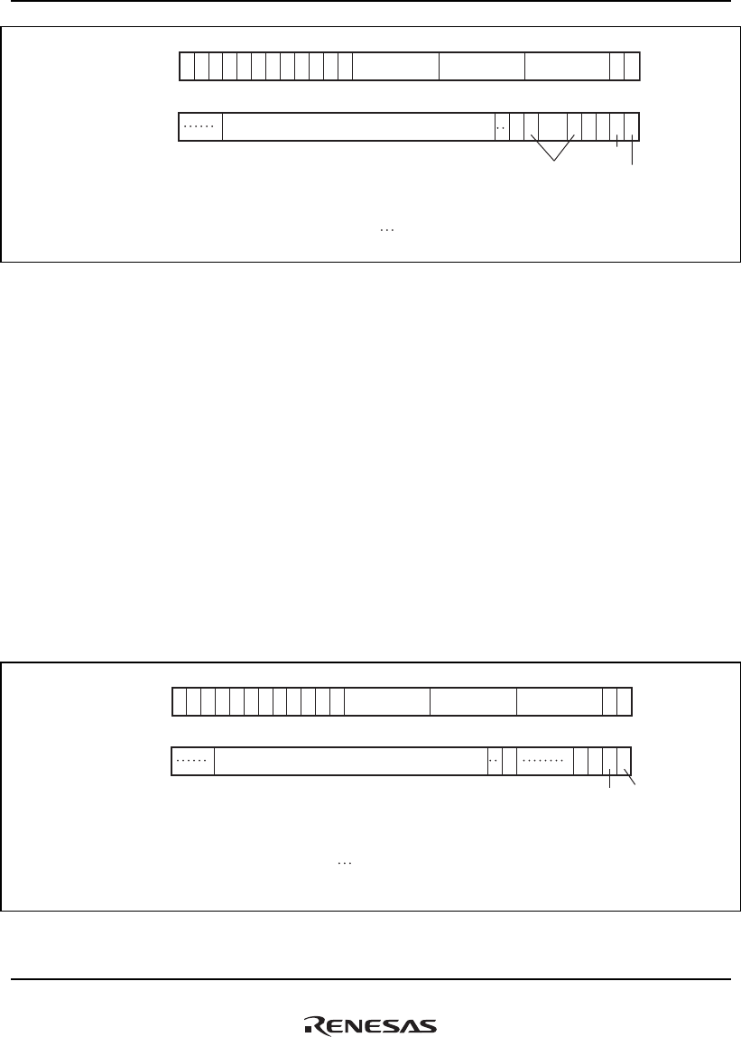
7. Memory Management Unit (MMU)
Rev.1.00 Jan. 10, 2008 Page 197 of 1658
REJ09B0261-0100
Address field
Data field
PPN:
V:
E:
SZ:
D:
*
:
Physical page number
Validity bit
Entry
Page size bits
Dirty bit
Don't care
PR:
C:
SH:
WT:
:
Protection key data
Cacheability bit
Share status bit
Write-through bit
Reserved bits
(write value should be 0
and read value is undefined )
31 21
21
0
V
1098729 28 4 365
PR CPPN D
SZ1
SH
WT
31 0
111101110000 00E
1920 8 714 13
******
** ****
Figure 7.23 Memory-Mapped UTLB Data Array (TLB Compatible Mode)
7.7.6 UTLB Data Array (TLB Extended Mode)
In TLB extended mode, the names of the data arrays have been changed from UTLB data array to
UTLB data array 1, UTLB data array 2 is added, and the EPR and ESZ bits are accessible. In TLB
extended mode, the PR and SZ bits of UTLB data array 1 are reserved and 0 should be specified
as the write value for these bits. In addition, when a write to UTLB data array 1 is performed, a
write to UTLB data array 2 of the same entry should always be performed after that.
In TLB compatible mode (MMUCR.ME = 0), UTLB data array 2 cannot be accessed. Operation if
they are accessed is not guaranteed.
(1) UTLB Data Array 1
In TLB extended mode, bits 7 to 4 in the data field, which correspond to the PR and SZ bits in
compatible mode, are reserved. Specify 0 as the write value for these bits.
Legend:
Address field
Data field
PPN:
V:
E:
D:
*:
Physical page number
Validity bit
Entry
Dirty bit
Don't care
C:
SH:
WT:
:
Cacheability bit
Share status bit
Write-through bit
Reserved bits
(write value should be 0,
and read value is undefined)
31 210
V
1098729 28
21
43
CDPPN
31 0
00
11110111
0
00
0
E
20 19 8 714 13
WTSH
******
*** ***
Figure 7.24 Memory-Mapped UTLB Data Array 1 (TLB Extended Mode)
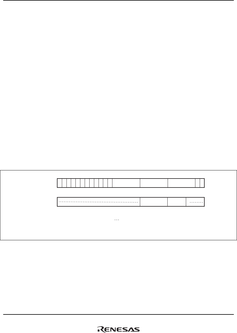
7. Memory Management Unit (MMU)
Rev.1.00 Jan. 10, 2008 Page 198 of 1658
REJ09B0261-0100
(2) UTLB Data Array 2
The UTLB data array is allocated to addresses H'F780 0000 to H'F78F FFFF in the P4 area.
Access to data array 2 requires a 32-bit address field specification (when reading or writing) and a
32-bit data field specification (when writing). Information for selecting the entry to be accessed is
specified in the address field, and EPR and ESZ to be written to data array 2 are specified in the
data field.
In the address field, bits [31:20] have the value H'F78 indicating UTLB data array 2 and the entry
is specified by bits [13:8].
In the data field, bits [13:8] indicate EPR, and bits [7:4] indicate ESZ, respectively.
The following two kinds of operation can be applied to UTLB data array 2:
1. UTLB data array 2 read
EPR and ESZ are read into the data field from the UTLB entry corresponding to the entry set
in the address field.
2. UTLB data array 2 write
EPR and ESZ specified in the data field are written to the UTLB entry corresponding to the
entry set in the address field.
Legend:
00
0
20 19
Address field
Data field
31 0
EPR ESZ
87
21
43
31 0
00
11110111
1
E
8714 13
13
******
*** ***
E:
EPR:
ESZ:
*:
Entry
Protection key data
Page size bits
Don't care
Reserved bits
(write value should be 0,
and read value is undefined)
:
Figure 7.25 Memory-Mapped UTLB Data Array 2 (TLB Extended Mode)
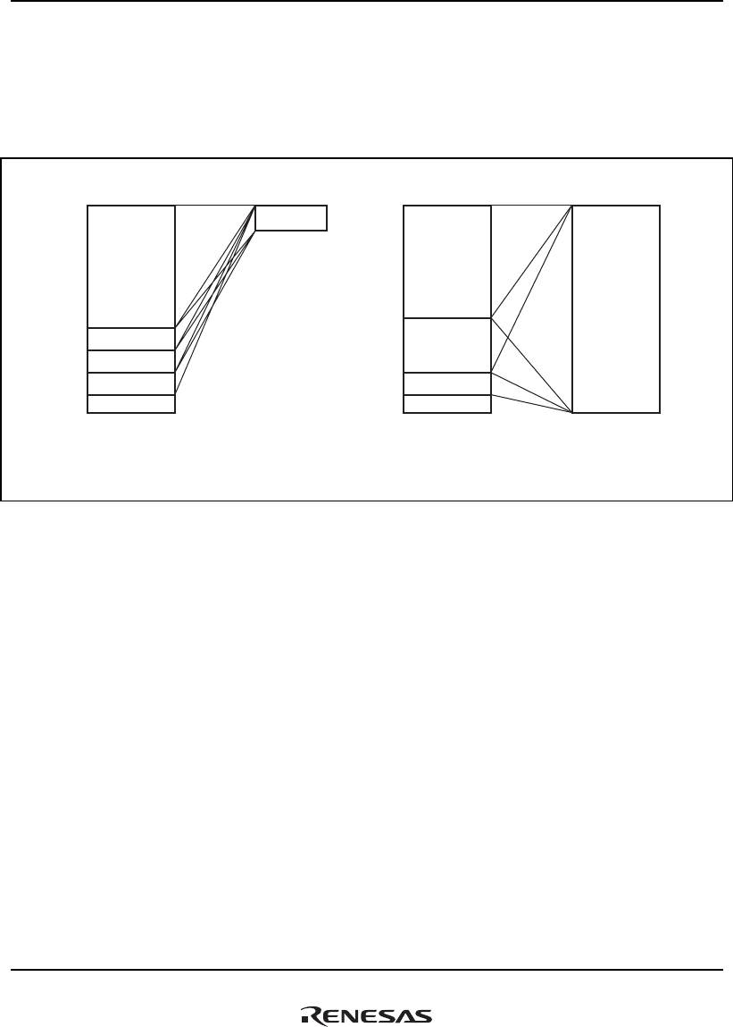
7. Memory Management Unit (MMU)
Rev.1.00 Jan. 10, 2008 Page 199 of 1658
REJ09B0261-0100
7.8 32-Bit Address Extended Mode
Setting the SE bit in PASCR to 1 changes mode from 29-bit address mode which handles the 29-
bit physical address space to 32-bit address extended mode which handles the 32-bit physical
address space.
P1 (0.5 Gbyte) P1/P2
(1 Gbyte)
0.5 Gbyte
4 Gbytes
U0/P0
(2 Gbytes)
U0/P0
(2 Gbytes)
P2 (0.5 Gbyte)
P3 (0.5 Gbyte) P3 (0.5 Gbyte)
P4 (0.5 Gbyte) P4 (0.5 Gbyte)
Virtual address space 29-bits
address space Virtual address space 32-bit
address space
29-bit Physical address space
(Normal mode)
32-bit Physical address space
(Extended mode)
Figure 7.26 Physical Address Space (32-Bit Address Extended Mode)
7.8.1 Overview of 32-Bit Address Extended Mode
In 32-bit address extended mode, the privileged space mapping buffer (PMB) is introduced. The
PMB maps virtual addresses in the P1 or P2 area which are not translated in 29-bit address mode
to the 32-bit physical address space. In areas which are target for address translation of the TLB
(UTLB/ITLB), upper three bits in the PPN field of the UTLB or ITLB are extended and then
addresses after the TLB translation can handle the 32-bit physical addresses.
As for the cache operation, P1 area is cacheable and P2 area is non-cacheable in the case of 29-bit
address mode, but the cache operation of both P1 and P2 area are determined by the C bit and WT
bit in the PMB in the case of 32-bit address mode.
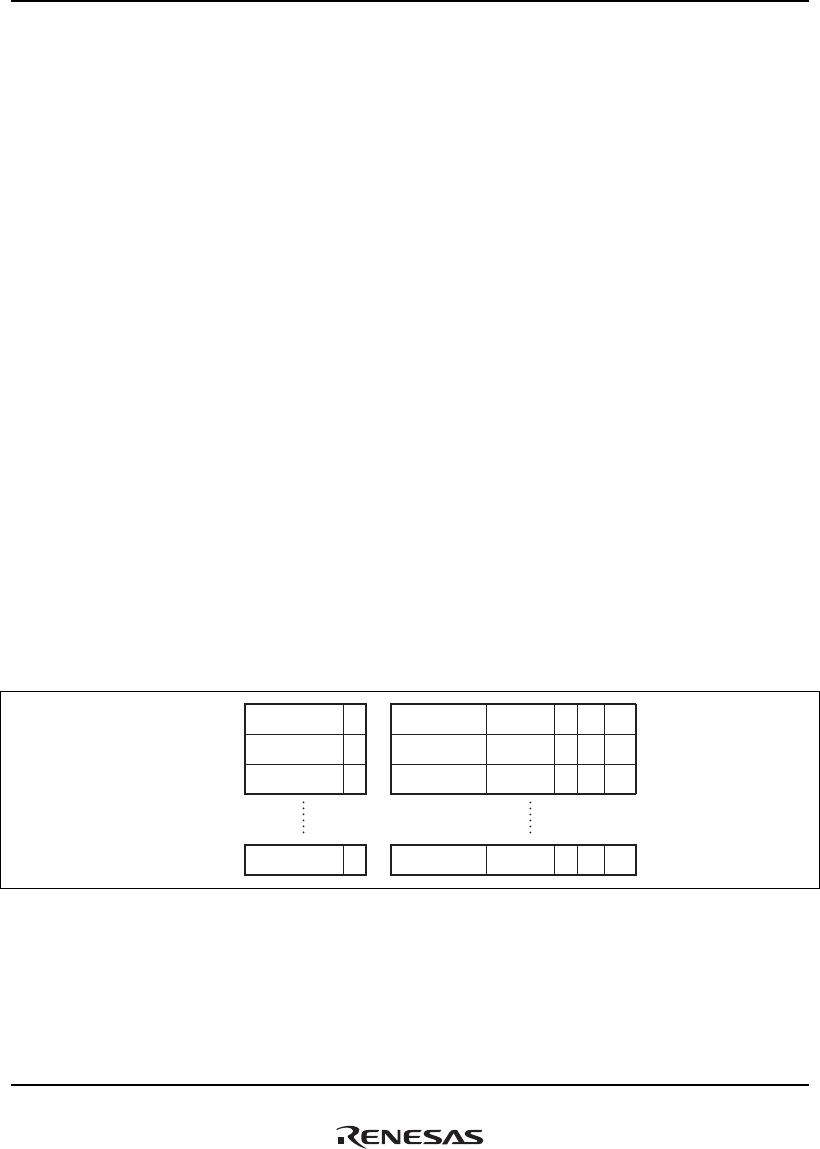
7. Memory Management Unit (MMU)
Rev.1.00 Jan. 10, 2008 Page 200 of 1658
REJ09B0261-0100
7.8.2 Transition to 32-Bit Address Extended Mode
This LSI enters 29-bit address mode after a power-on reset. Transition is made to 32-bit address
extended mode by setting the SE bit in PASCR to 1. In 32-bit address extended mode, the MMU
operates as follows.
1. When the AT bit in MMUCR is 0, virtual addresses in the U0, P0, or P3 area become 32-bit
physical addresses. Addresses in the P1 or P2 area are translated according to the PMB
mapping information. B'10 should be set to the upper 2 bits of virtual page number
(VPN[31:30]) in the PMB in order to indicate P1 or P2 area. The operation is not guaranteed
when the value except B'10 is set to these bits.
2. When the AT bit in MMUCR is 1, virtual addresses in the U0, P0, or P3 area are translated to
32-bit physical addresses according to the TLB conversion information. Addresses in the P1 or
P2 area are translated according to the PMB mapping information. B'10 should be set to the
upper 2 bits of virtual page number (VPN[31:30]) in the PMB in order to indicate P1 or P2
area. The operation is not guaranteed when the value except B'10 is set to these bits.
3. Regardless of the setting of the AT bit in MMUCR, bits 31 to 29 in physical addresses become
B'111 in the control register area (addresses H'FC00 0000 to H'FFFF FFFF). When the control
register area is recorded in the UTLB and accessed, B'111 should be set to PPN[31:29].
7.8.3 Privileged Space Mapping Buffer (PMB) Configuration
In 32-bit address extended mode, virtual addresses in the P1 or P2 area are translated according to
the PMB mapping information. The PMB has 16 entries and configuration of each entry is as
follows.
PPN[31:24]
PPN[31:24]
PPN[31:24]
SZ[1:0]
SZ[1:0]
SZ[1:0]
C
C
C
UB
UB
UB
VPN[31:24]
VPN[31:24]
VPN[31:24]
V
V
V
Entry 0
Entry 1
Entry 2
WT
WT
WT
PPN[31:24] SZ[1:0] C UBVPN[31:24] VEntry 15 WT
Figure 7.27 PMB Configuration

7. Memory Management Unit (MMU)
Rev.1.00 Jan. 10, 2008 Page 201 of 1658
REJ09B0261-0100
Legend:
• VPN: Virtual page number
For 16-Mbyte page: Upper 8 bits of virtual address
For 64-Mbyte page: Upper 6 bits of virtual address
For 128-Mbyte page: Upper 5 bits of virtual address
For 512-Mbyte page: Upper 3 bits of virtual address
Note: B'10 should be set to the upper 2 bits of VPN in order to indicate P1 or P2 area.
• SZ: Page size bits
Specify the page size.
00: 16-Mbyte page
01: 64-Mbyte page
10: 128-Mbyte page
11: 512-Mbyte page
• V: Validity bit
Indicates whether the entry is valid.
0: Invalid
1: Valid
Cleared to 0 by a power-on reset.
Not affected by a manual reset.
• PPN: Physical page number
Upper 8 bits of the physical address of the physical page number.
With a 16-Mbyte page, PPN[31:24] are valid.
With a 64-Mbyte page, PPN[31:26] are valid.
With a 128-Mbyte page, PPN[31:27] are valid.
With a 512-Mbyte page, PPN[31:29] are valid.
• C: Cacheability bit
Indicates whether a page is cacheable.
0: Not cacheable
1: Cacheable

7. Memory Management Unit (MMU)
Rev.1.00 Jan. 10, 2008 Page 202 of 1658
REJ09B0261-0100
• WT: Write-through bit
Specifies the cache write mode.
0: Copy-back mode
1: Write-through mode
• UB: Buffered write bit
Specifies whether a buffered write is performed.
0: Buffered write (Data access of subsequent processing proceeds without waiting for the write
to complete.)
1: Unbuffered write (Data access of subsequent processing is stalled until the write has
completed.)
7.8.4 PMB Function
This LSI supports the following PMB functions.
1. Only memory-mapped write can be used for writing to the PMB. The LDTLB instruction
cannot be used to write to the PMB.
2. Software must ensure that every accessed P1 or P2 address has a corresponding PMB entry
before the access occurs. When an access to an address in the P1 or P2 area which is not
recorded in the PMB is made, this LSI is reset by the TLB. In this case, the accessed address in
the P1 or P2 area which causes the TLB reset is stored in the TEA and code H′140 in the
EXPEVT.
3. The SH-4A does not guarantee the operation when multiple hit occurs in the PMB. Special
care should be taken when the PMB mapping information is recorded by software.
4. The PMB does not have an associative write function.
5. Since there is no PR field in the PMB, read/write protection cannot be preformed. The address
translation target of the PMB is the P1 or P2 address. In user mode access, an address error
exception occurs.
6. Both entries from the UTLB and PMB are mixed and recorded in the ITLB by means of the
hardware ITLB miss handling. However, these entries can be identified by checking whether
VPN[31:30] is 10 or not. When an entry from the PMB is recorded in the ITLB, H′00, 01, and
1 are recorded in the ASID, PR, and SH fields which do not exist in the PMB, respectively.

7. Memory Management Unit (MMU)
Rev.1.00 Jan. 10, 2008 Page 203 of 1658
REJ09B0261-0100
7.8.5 Memory-Mapped PMB Configuration
To enable the PMB to be managed by software, its contents are allowed to be read from and
written to by a P1 or P2 area program with a MOV instruction in privileged mode. The PMB
address array is allocated to addresses H'F610 0000 to H'F61F FFFF in the P4 area and the PMB
data array to addresses H'F710 0000 to H'F71F FFFF in the P4 area. VPN and V in the PMB can
be accessed as an address array, PPN, V, SZ, C, WT, and UB as a data array. V can be accessed
from both the address array side and the data array side. A program which executes a PMB
memory-mapped access should be placed in the page area at which the C bit in PMB is cleared to
0.
1. PMB address array read
When memory reading is performed while bits 31 to 20 in the address field are specified as
H'F61 which indicates the PMB address array and bits 11 to 8 in the address field as an entry,
bits 31 to 24 in the data field are read as VPN and bit 8 in the data field as V.
2. PMB address array write
When memory writing is performed while bits 31 to 20 in the address field are specified as
H'F61 which indicates the PMB address array and bits 11 to 8 in the address field as an entry,
and bits 31 to 24 in the data field are specified as VPN and bit 8 in the data field as V, data is
written to the specified entry.
3. PMB data array read
When memory reading is performed while bits 31 to 20 in the address field are specified as
H'F71 which indicates the PMB data array and bits 11 to 8 in the address field as an entry, bits
31 to 24 in the data field are read as PPN, bit 9 in the data field as UB, bit 8 in the data field as
V, bits 7 and 4 in the data field as SZ, bit 3 in the data field as C, and bit 0 in the data field as
WT.
4. PMB data array write
When memory writing is performed while bits 31 to 20 in the address field are specified as
H'F71 which indicates the PMB data array and bits 11 to 8 in the address field as an entry, and
bits 31 to 24 in the data field are specified as PPN, bit 9 in the data field as UB, bit 8 in the
data field as V, bits 7 and 4 in the data field as SZ, bit 3 in the data field as C, and bit 0 in the
data field as WT, data is written to the specified entry.
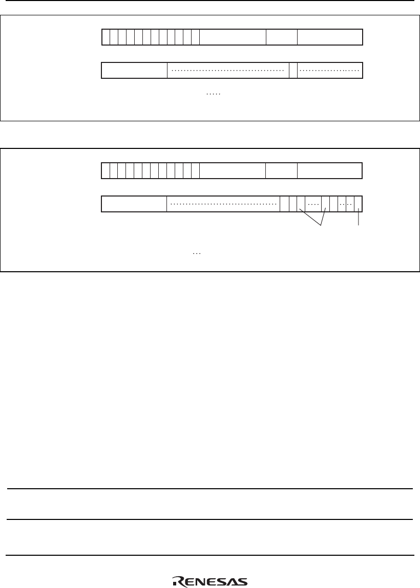
7. Memory Management Unit (MMU)
Rev.1.00 Jan. 10, 2008 Page 204 of 1658
REJ09B0261-0100
Address field
Data field
VPN:
V:
E:
Physical page number
Validity bit
Entry
: Reserved bits (write value should be 0
and read value is undefined )
31 0
V
8
87
VPN
31 1920 0
11110 0001101 00E
2324
12 11
00000 00000000 0
Figure 7.28 Memory-Mapped PMB Address Array
Address field
Data field
PPN:
V:
E:
SZ:
Physical page number
Validity bit
Entry
Page size bits
UB:
C:
WT:
:
Buffered write bit
Cacheability bit
Write-throu
gh bit
Reserved bits
(write value should be 0
and read value is undefined )
31 210
V
UB
10 9 8 74365
C
PPN
31 0
111101110001 E
2324
1920 8 712 11
SZ WT
00000000 00000000
Figure 7.29 Memory-Mapped PMB Data Array
7.8.6 Notes on Using 32-Bit Address Extended Mode
When using 32-bit address extended mode, note that the items described in this section are
extended or changed as follows.
(1) PASCR
The SE bit is added in bit 31 in the control register (PASCR). The bits 6 to 0 of the UB in the
PASCR are invalid (Note that the bit 7 of the UB is still valid). When writing to the P1 or P2 area,
the UB bit in the PMB controls whether a buffered write is performed or not. When the MMU is
enabled, the UB bit in the TLB controls writing to the P0, P3, or U0 area. When the MMU is
disabled, writing to the P0, P3, or U0 area is always performed as a buffered write.
Bit Bit Name
Initial
Value R/W Description
31 SE 0 R/W 0: 29-bit address mode
1: 32-bit address extended mode

7. Memory Management Unit (MMU)
Rev.1.00 Jan. 10, 2008 Page 205 of 1658
REJ09B0261-0100
Bit Bit Name
Initial
Value R/W Description
30 to 8 ⎯ All 0 R Reserved
For details on reading from or writing to these bits, see
description in General Precautions on Handling of
Product.
7 to 0 UB All 0 R/W Buffered Write Control for Each Area (64 Mbytes)
When writing is performed without using the cache or in
the cache write-through mode, these bits specify
whether the CPU waits for the end of writing for each
area.
0: The CPU does not wait for the end of writing
1: The CPU stalls and waits for the end of writing
UB[7]: Corresponding to the control register area
UB[6:0]: These bits are invalid in 32-bit address
extended mode.
(2) ITLB
The PPN field in the ITLB is extended to bits 31 to 10.
(3) UTLB
The PPN field in the UTLB is extended to bits 31 to 10. The same UB bit as that in the PMB is
added in each entry of the UTLB.
• UB: Buffered write bit
Specifies whether a buffered write is performed.
0: Buffered write (Subsequent processing proceeds without waiting for the write to complete.)
1: Unbuffered write (Subsequent processing is stalled until the write has completed.)
In a memory-mapped TLB access, the UB bit can be read from or written to by bit 9 in the data
array.
(4) PTEL
The same UB bit as that in the PMB is added in bit 9 in PTEL. This UB bit is written to the UB bit
in the UTLB by the LDTLB instruction. The PPN field is extended to bits 31 to 10.

7. Memory Management Unit (MMU)
Rev.1.00 Jan. 10, 2008 Page 206 of 1658
REJ09B0261-0100
(5) CCR.CB
The CB bit in CCR is invalid. Whether a cacheable write for the P1 area is performed in copy-
back mode or write-though mode is determined by the WT bit in the PMB.
(6) IRMCR.MT
The MT bit in IRMCR is valid for a memory-mapped PMB write.
(7) QACR0, QACR1
AREA0[4:2]/AREA1[4:2] fields of QACR0/QACR1 are extended to AREA0[7:2]/AREA1[7:2]
corresponding to physical address [31:26].
(8) LSA0, LSA1, LDA0, LDA1
L0SADR, L1SADR, L0DADR, and L1DADR fields are extended to bits 31 to 10.
When using 32-bit address mode, the following notes should be applied to software.
1. For the SE bit switching, switching from 0 to 1 is only supported in a boot routine which is
allocated in an area where caching and TLB-based address translation are not allowed and runs
after a power-on reset or manual reset.
2. After switching the SE bit, an area in which the program is allocated becomes the target of the
PMB address translation. Therefore, the area should be recorded in the PMB before switching
the SE bit. An address which may be accessed in the P1 or P2 area such as the exception
handler should also be recorded in the PMB.
3. When an external memory access occurs by an operand memory access located before the
MOV.L instruction which switches the SE bit, external memory space addresses accessed in
both address modes should be the same.
4. Note that the V bit is mapped to both address array and data array in PMB registration. That is,
first write 0 to the V bit in one of arrays and then write 1 to the V bit in another array.

7. Memory Management Unit (MMU)
Rev.1.00 Jan. 10, 2008 Page 207 of 1658
REJ09B0261-0100
7.9 32-Bit Boot Function
The address mode of this LSI after a power-on reset or manual reset can be switched between 29-
bit address mode and 32-bit address extended mode by specifying external pins. The following
changes apply when this LSI is booted up in 32-bit address extended mode.
7.9.1 Initial Entries to PMB
When 32-bit address extended mode is specified by external pins, the following initial entries are
recorded in the PMB after a power-on reset or manual reset, and the SE bit in the PASCR register
is initialized to 1. For entries 2 to 15, only the V bit is initialized to 0.
Entry VPN[31:24] PPN[31:24] V SZ[1:0] C UB WT
0 10000000 00000000 1 11 1 0 1
1 10100000 00000000 1 11 0 0 0
7.9.2 Notes on 32-Bit Boot
Immediately after a power-on or manual reset, the P1 or P2 area is mapped to the PMB. Therefore,
when an area other than that indicated by the initial entry needs to be mapped, follow the
procedures below to modify the PMB, taking care not to generate PMB misses and multiple PMB
hits. The procedure should be set up within the boot routine and should be executed before
activation of the caches and TLB (CCR.ICE = 1, CCR.OCE = 1, and MMUCR.AT = 1). Do not
use routines other than the boot routine to change the value recorded in the PMB.
(1) When the Program Modifying the PMB is in the P1 or P2 Area
1. Read the initial entry, change only the SZ bits to reduce the page size, and save the new value
over the previous entry. The program that changes the PMB should be allocated within 1
Mbyte of the top of the page with the reduced size.
2. Invalidate the entry remaining in the ITLB that corresponds to the PMB by writing 1 to the TI
bit in the MMUCR register.
3. In the memory-mapped PMB, record PMB entries to fill the P1 or P2 area in which the PMB
translation information is evicted by step 1.
4. Execute one of the following steps, A, B, and C. Do not execute a branch or operand access for
the P1 or P2 area in which the PMB translation information is evicted by step 1.
A. Perform a branch using the RTE instruction.
B. Execute the ICBI instruction for any address (including non-cacheable area).

7. Memory Management Unit (MMU)
Rev.1.00 Jan. 10, 2008 Page 208 of 1658
REJ09B0261-0100
C. If the MT bit in IRMCR is set to 0 (initial value) before accessing the memory-mapped
PMB, no specific sequence is required.
However, correct operation with method C may no longer be guaranteed in future SuperH-
family products. Selection of step A or B is recommended to ensure compatibility with future
SuperH-family products.
(2) When the Program Modifying the PMB is in Areas Other than the P1 or P2 Area
1. Invalidate the entry remaining in the ITLB by writing 1 to the TI bit in MMUCR.
2. In the memory-mapped PMB, change PMB entries.
3. Execute one of the following steps, A, B, and C. Do not execute a branch or operand access for
the P1 or P2 area before this execution.
A. Perform a branch using the RTE instruction.
B. Execute the ICBI instruction for any address (including non-cacheable area).
C. If the MT bit in IRMCR is set to 0 (initial value) before accessing the memory-mapped
PMB, no specific sequence is required.
However, correct operation with method C may no longer be guaranteed in future SuperH-
family products. Selection of step A or B is recommended to ensure compatibility with future
SuperH-family products.

7. Memory Management Unit (MMU)
Rev.1.00 Jan. 10, 2008 Page 209 of 1658
REJ09B0261-0100
7.10 Usage Notes
7.10.1 Note on Using LDTLB Instruction
When using an LDTLB instruction instead of software to a value to the MMUCR. URC, execute 1
or 2 below.
1. In 29-bit address mode, follow A. and B. below. In 32-bit address mode, follow A. through D.
below.
A. Place the TLB miss exception handling routine*1 only in the P1, P2 area ,or the on-chip
memory so that all the instruction accesses*3 in the TLB miss exception handling routine
should occur solely in the P1, P2 area, or the on-chip memory. Clear the RP bit in the
RAMCR register to 0 (initial value), when the TLB miss exception handling routine is
placed in the on-chip memory.
B. Use only one page of the PMB for instruction accesses*3 in the TLB miss exception
handling routine*1. In 32-bit address mode, do not place them in the last 64 bytes of a page
of the PMB.
C. In 32-bit address mode, obey 1 and 2 below when recording information in the UTLB in
the MMU-related exception*2 handling routine.
a. When thea TLB miss exception occurs, and recording the information of a page with
the access right in the UTLB, do not record the page, in which the exception has
occurred, in the UTLB using the following two operations.
⎯ Specifies the protection key data that causes a protection violation exception upon
re-execution of the instruction that has caused the TLB miss exception and records
the page, in which the TLB miss exception has occurred, in the UTLB.
⎯ Specifies the protection key data that does not cause a protection violation
exception in the protection violation exception handling routine to record the page
in the UTLB and re-executes the instruction that has caused the protection violation
exception.
b. When an initial page write exception occurs and the TLB entry in the UTLB of which
the dirty bit is 1 is replaced, before the write instruction for the page corresponding to
this replaced TLB entry is completed, register the TLB entry of which the dirty bit is 1.
D. Do not make an attempt to execute the FDIV or FSQRT instruction in the TLB miss
exception handling routine.
2. If a TLB miss exception occurs, add 1 to MMUCR.URC before executing an LDTLB
instruction.

7. Memory Management Unit (MMU)
Rev.1.00 Jan. 10, 2008 Page 210 of 1658
REJ09B0261-0100
Notes: 1. An exception handling routine is an entire set of instructions that are executed from the
address (VBR + offset) upon occurrence of an exception to the RTE for returning to the
original program or to the RTE delay slot.
2. MMU-related exceptions are: instruction TLB miss exception, instruction TLB miss
protection violation exception, data TLB miss exception, data TLB protection violation
exception, and initial page write exception.
3. Instruction accesses include the PREFI and ICBI instructions.

8. Caches
Rev.1.00 Jan. 10, 2008 Page 211 of 1658
REJ09B0261-0100
Section 8 Caches
This LSI has an on-chip 32-Kbyte instruction cache (IC) for instructions and an on-chip 32-Kbyte
operand cache (OC) for data.
8.1 Features
The features of the cache are given in table 8.1.
This LSI supports two 32-byte store queues (SQs) to perform high-speed writes to external
memory. The features of the store queues are given in table 8.2.
Table 8.1 Cache Features
Item Instruction Cache Operand Cache
Capacity 32-Kbyte cache 32-Kbyte cache
Type 4-way set-associative, virtual
address index/physical address tag
4-way set-associative, virtual
address index/physical address tag
Line size 32 bytes 32 bytes
Entries 256 entries/way 256 entries/way
Write method ⎯ Copy-back/write-through selectable
Replacement method LRU (least-recently-used) algorithm LRU (least-recently-used) algorithm
Table 8.2 Store Queue Features
Item Store Queues
Capacity 32 bytes × 2
Addresses H'E000 0000 to H'E3FF FFFF
Write Store instruction (1-cycle write)
Write-back Prefetch instruction (PREF instruction)
Access right When MMU is disabled: Determined by SQMD bit in MMUCR
When MMU is enabled: Determined by PR for each page
The operand cache of this LSI is 4-way set associative, each may comprising 256 cache lines.
Figure 8.1 shows the configuration of the operand cache.
The instruction cache is 4-way set-associative, each way comprising 256 cache lines. Figure 8.2
shows the configuration of the instruction cache.
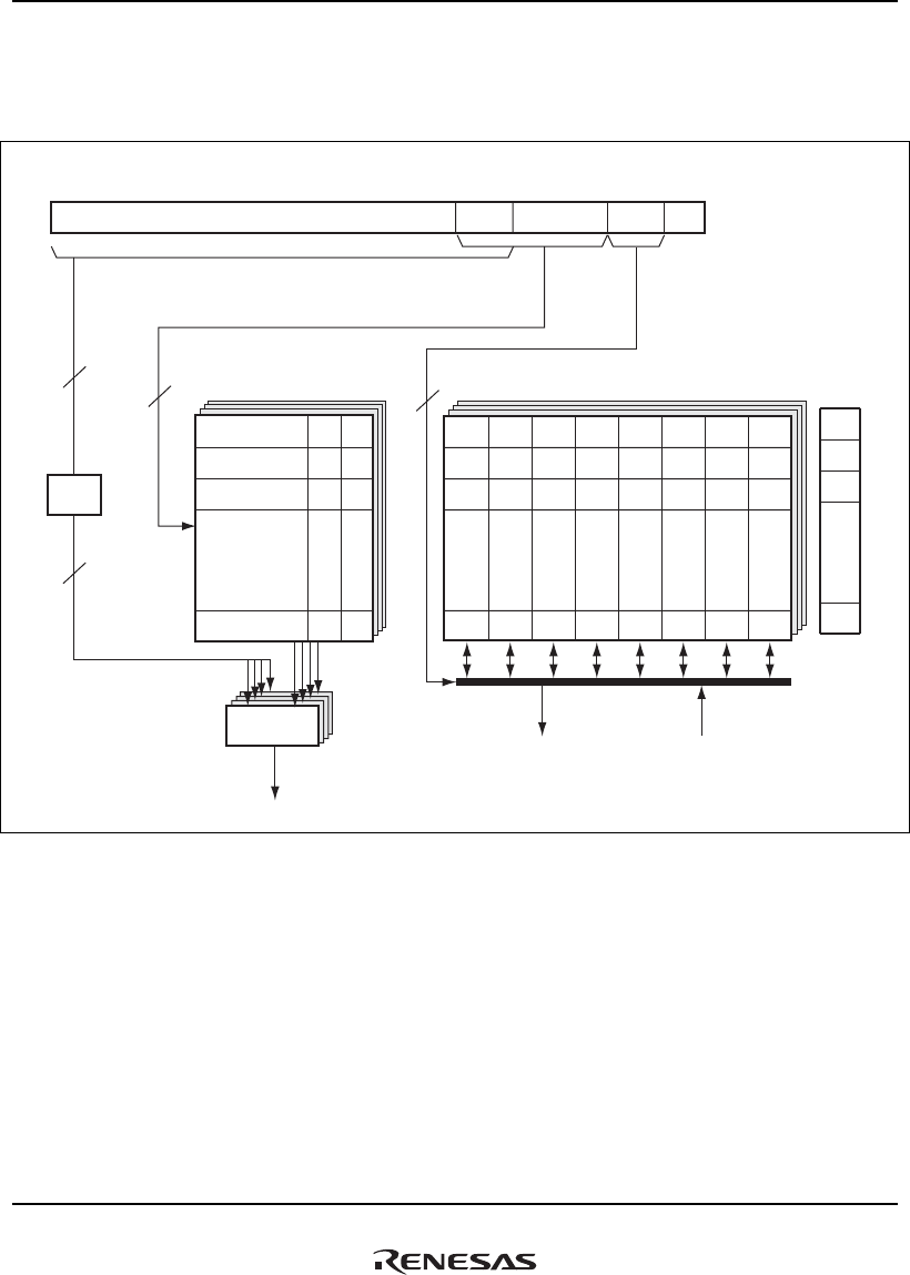
8. Caches
Rev.1.00 Jan. 10, 2008 Page 212 of 1658
REJ09B0261-0100
This LSI has an IC way prediction scheme to reduce power consumption. In addition, memory-
mapped associative writing, which is detectable as an exception, can be enabled by using the non-
support detection exception register (EXPMASK). For details, see section 5, Exception Handling.
31 54 2
LW0
32 bits
LW1
32 bits
LW2
32 bits
LW3
32 bits
LW4
32 bits
LW5
32 bits
LW6
32 bits
LW7
32 bits 6 bits
MMU
[12:5]
255 19 bits 1 bit 1 bit
TagUV
Address array
(way 0 to way 3)
Data array
(way 0 to way3) LRU
Entry selection Longword (LW) selection
Virtual address
3
8
22
19
0
Write data
Read data
Hit signal
(Way 0 to way 3)
12 10 0
Comparison
Figure 8.1 Configuration of Operand Cache (Cache size = 32 Kbytes)

8. Caches
Rev.1.00 Jan. 10, 2008 Page 213 of 1658
REJ09B0261-0100
31 54 2
LW0
32 bits
LW1
32 bits
LW2
32 bits
LW3
32 bits
LW4
32 bits
LW5
32 bits
LW6
32 bits
LW7
32 bits
MMU
[12:5]
255 19 bits 1 bit
TagV
Address array
(way 0 to way 3)
Data array
(way 0 to way3)
Entry selection
Longword (LW) selection
Virtual address
3
8
22
19
0
Read data
13 12 10 0
6 bits
LRU
Hit signal
(Way 0 to way 3)
Comparison
Figure 8.2 Configuration of Instruction Cache (Cache size = 32 Kbytes)
• Tag
Stores the upper 19 bits of the 29-bit physical address of the data line to be cached. The tag is
not initialized by a power-on or manual reset.
• V bit (validity bit)
Indicates that valid data is stored in the cache line. When this bit is 1, the cache line data is
valid. The V bit is initialized to 0 by a power-on reset, but retains its value in a manual reset.
• U bit (dirty bit)
The U bit is set to 1 if data is written to the cache line while the cache is being used in copy-
back mode. That is, the U bit indicates a mismatch between the data in the cache line and the
data in external memory. The U bit is never set to 1 while the cache is being used in write-
through mode, unless it is modified by accessing the memory-mapped cache (see section 8.6,
Memory-Mapped Cache Configuration). The U bit is initialized to 0 by a power-on reset, but
retains its value in a manual reset.

8. Caches
Rev.1.00 Jan. 10, 2008 Page 214 of 1658
REJ09B0261-0100
• Data array
The data field holds 32 bytes (256 bits) of data per cache line. The data array is not initialized
by a power-on or manual reset.
• LRU
In a 4-way set-associative method, up to 4 items of data can be registered in the cache at each
entry address. When an entry is registered, the LRU bit indicates which of the 4 ways it is to be
registered in. The LRU mechanism uses 6 bits of each entry, and its usage is controlled by
hardware. The LRU (least-recently-used) algorithm is used for way selection, and selects the
less recently accessed way. The LRU bits are initialized to 0 by a power-on reset but not by a
manual reset. The LRU bits cannot be read from or written to by software.

8. Caches
Rev.1.00 Jan. 10, 2008 Page 215 of 1658
REJ09B0261-0100
8.2 Register Descriptions
The following registers are related to cache.
Table 8.3 Register Configuration
Register Name Abbreviation R/W P4 Address* Area 7 Address* Size
Cache control register CCR R/W H'FF00 001C H'1F00 001C 32
Queue address control register 0 QACR0 R/W H'FF00 0038 H'1F00 0038 32
Queue address control register 1 QACR1 R/W H'FF00 003C H'1F00 003C 32
On-chip memory control register RAMCR R/W H'FF00 0074 H'1F00 0074 32
Note: * These P4 addresses are for the P4 area in the virtual address space. These area 7
addresses are accessed from area 7 in the physical address space by means of the
TLB.
Table 8.4 Register States in Each Processing State
Register Name Abbreviation Power-on Reset Manual Reset Sleep Standby
Cache control register CCR H'0000 0000 H'0000 0000 Retained Retained
Queue address control register 0 QACR0 Undefined Undefined Retained Retained
Queue address control register 1 QACR1 Undefined Undefined Retained Retained
On-chip memory control register RAMCR H'0000 0000 H'0000 0000 Retained Retained
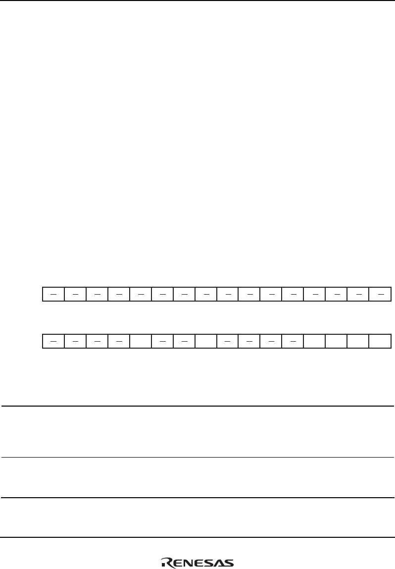
8. Caches
Rev.1.00 Jan. 10, 2008 Page 216 of 1658
REJ09B0261-0100
8.2.1 Cache Control Register (CCR)
CCR controls the cache operating mode, the cache write mode, and invalidation of all cache
entries.
CCR modifications must only be made by a program in the non-cacheable P2 area or IL memory.
After CCR has been updated, execute one of the following three methods before an access
(including an instruction fetch) to the cacheable area is performed.
1. Execute a branch using the RTE instruction. In this case, the branch destination may be the
cacheable area.
2. Execute the ICBI instruction for any address (including non-cacheable area).
3. If the R2 bit in IRMCR is 0 (initial value) before updating CCR, the specific instruction does
not need to be executed. However, note that the CPU processing performance will be lowered
because the instruction fetch is performed again for the next instruction after CCR has been
updated.
Note that the method 3 may not be guaranteed in the future SuperH Series. Therefore, it is
recommended that the method 1 or 2 should be used for being compatible with the future SuperH
Series.
31 30 29 28 27 26 25 24 23 22 21 20 19 18 17 16
Bit:
0000000000000000
Initial value:
RRRRRRRRRRRRRRRR
R R R R R/W R R R/W R R R R R/W R/W R/W R/W
R/W:
Bit:
Initial value:
R/W:
15 14 13 12 11 10 9 8 7 6 5 4 3 2 1 0
00000000 0000 000
ICI ICE OCEWTCBOCI
0
Bit Bit Name
Initial
Value R/W Description
31 to 12 ⎯ All 0 R Reserved
For details on reading from or writing to these bits, see
description in General Precautions on Handling of
Product.
11 ICI 0 R/W IC Invalidation Bit
When 1 is written to this bit, the V bits of all IC entries
are cleared to 0. This bit is always read as 0.

8. Caches
Rev.1.00 Jan. 10, 2008 Page 217 of 1658
REJ09B0261-0100
Bit Bit Name
Initial
Value R/W Description
10, 9 ⎯ All 0 R Reserved
For details on reading from or writing to these bits, see
description in General Precautions on Handling of
Product.
8 ICE 0 R/W IC Enable Bit
Selects whether the IC is used. Note however when
address translation is performed, the IC cannot be used
unless the C bit in the page management information is
also 1.
0: IC not used
1: IC used
7 to 4 ⎯ All 0 R Reserved
For details on reading from or writing to these bits, see
description in General Precautions on Handling of
Product.
3 OCI 0 R/W OC Invalidation Bit
When 1 is written to this bit, the V and U bits of all OC
entries are cleared to 0. This bit is always read as 0.
2 CB 0 R/W Copy-Back Bit
Indicates the P1 area cache write mode.
0: Write-through mode
1: Copy-back mode
1 WT 0 R/W Write-Through Mode
Indicates the P0, U0, and P3 area cache write mode.
When address translation is performed, the value of the
WT bit in the page management information has
priority.
0: Copy-back mode
1: Write-through mode
0 OCE 0 R/W OC Enable Bit
Selects whether the OC is used. Note however when
address translation is performed, the OC cannot be
used unless the C bit in the page management
information is also 1.
0: OC not used
1: OC used

8. Caches
Rev.1.00 Jan. 10, 2008 Page 218 of 1658
REJ09B0261-0100
8.2.2 Queue Address Control Register 0 (QACR0)
QACR0 specifies the area onto which store queue 0 (SQ0) is mapped when the MMU is disabled.
31 30 29 28 27 26 25 24 23 22 21 20 19 18 17 16
Bit:
Initial value:
RRRRRRRRRRRRRRRR
0000000000000000
00000000000 00
R R R R R R R R R R R R/W R/W R/W R R
R/W:
Bit:
Initial value:
R/W:
15 14 13 12 11 10 9 8 7 6 5 4 3 2 1 0
AREA0
Bit Bit Name
Initial
Value R/W Description
31 to 5 ⎯ All 0 R Reserved
For details on reading from or writing to these bits, see
description in General Precautions on Handling of
Product.
4 to 2 AREA0 Undefined R/W When the MMU is disabled, these bits generate
physical address bits [28:26] for SQ0.
1, 0 ⎯ All 0 R Reserved
For details on reading from or writing to these bits, see
description in General Precautions on Handling of
Product.

8. Caches
Rev.1.00 Jan. 10, 2008 Page 219 of 1658
REJ09B0261-0100
8.2.3 Queue Address Control Register 1 (QACR1)
QACR1 specifies the area onto which store queue 1 (SQ1) is mapped when the MMU is disabled.
31 30 29 28 27 26 25 24 23 22 21 20 19 18 17 16
Bit:
Initial value:
RRRRRRRRRRRRRRRR
0000000000000000
00000000000 00
R R R R R R R R R R R R/W R/W R/W R R
R/W:
Bit:
Initial value:
R/W:
15 14 13 12 11 10 9 8 7 6 5 4 3 2 1 0
AREA1
Bit Bit Name
Initial
Value R/W Description
31 to 5 ⎯ All 0 R Reserved
For details on reading from or writing to these bits, see
description in General Precautions on Handling of
Product.
4 to 2 AREA1 Undefined R/W When the MMU is disabled, these bits generate
physical address bits [28:26] for SQ1.
1, 0 ⎯ All 0 R Reserved
For details on reading from or writing to these bits, see
description in General Precautions on Handling of
Product.

8. Caches
Rev.1.00 Jan. 10, 2008 Page 220 of 1658
REJ09B0261-0100
8.2.4 On-Chip Memory Control Register (RAMCR)
RAMCR controls the number of ways in the IC and OC and prediction of the IC way.
RAMCR modifications must only be made by a program in the non-cacheable P2 area. After
RAMCR has been updated, execute one of the following three methods before an access
(including an instruction fetch) to the cacheable area, the IL memory area, the OL memory area, or
the U memory area is performed.
1. Execute a branch using the RTE instruction. In this case, the branch destination may be the
non-cacheable area, the IL memory area, the OL memory area, or the U memory area.
2. Execute the ICBI instruction for any address (including non-cacheable area).
3. If the R2 bit in IRMCR is 0 (initial value) before updating RAMCR, the specific instruction
does not need to be executed. However, note that the CPU processing performance will be
lowered because the instruction fetch is performed again for the next instruction after RAMCR
has been updated.
Note that the method 3 may not be guaranteed in the future SuperH Series. Therefore, it is
recommended that the method 1 or 2 should be used for being compatible with the future SuperH
Series.
31 30 29 28 27 26 25 24 23 22 21 20 19 18 17 16
Bit:
Initial value:
RRRRRRRRRR
RMD RP IC2W OC2W
RRRRRR
0000000000000000
0000000000000000
R R R R R R R/W R/W R/W R/W R/W R R R R R
R/W:
Bit:
Initial value:
R/W:
15 14 13 12 11 10 9 8 7 6 5 4 3 2 1 0
ICWPW
Bit Bit Name
Initial
Value R/W Description
31 to 10 ⎯ All 0 R Reserved
For details on reading from or writing to these bits, see
description in General Precautions on Handling of
Product.
9 RMD 0 R/W On-Chip Memory Access Mode Bit
For details, see section 9.4, On-Chip Memory
Protective Functions.

8. Caches
Rev.1.00 Jan. 10, 2008 Page 221 of 1658
REJ09B0261-0100
Bit Bit Name
Initial
Value R/W Description
8 RP 0 R/W On-Chip Memory Protection Enable Bit
For details, see section 9.4, On-Chip Memory
Protective Functions.
7 IC2W 0 R/W IC Two-Way Mode bit
0: IC is a four-way operation
1: IC is a two-way operation
For details, see section 8.4.3, IC Two-Way Mode.
6 OC2W 0 R/W OC Two-Way Mode bit
0: OC is a four-way operation
1: OC is a two-way operation
For details, see section 8.3.6, OC Two-Way Mode.
5 ICWPD 0 R/W IC Way Prediction Stop
Selects whether the IC way prediction is used.
0: Instruction cache performs way prediction.
1: Instruction cache does not perform way prediction.
4 to 0 ⎯ All 0 R Reserved
For details on reading from or writing to these bits, see
description in General Precautions on Handling of
Product.

8. Caches
Rev.1.00 Jan. 10, 2008 Page 222 of 1658
REJ09B0261-0100
8.3 Operand Cache Operation
8.3.1 Read Operation
When the Operand Cache (OC) is enabled (OCE = 1 in CCR) and data is read from a cacheable
area, the cache operates as follows:
1. The tag, V bit, U bit, and LRU bits on each way are read from the cache line indexed by virtual
address bits [12:5].
2. The tags read from the each way is compared with bits [28:10] of the physical address
resulting from virtual address translation by the MMU:
⎯ If there is a way whose tag matches and its V bit is 1, see No. 3.
⎯ If there is no way whose tag matches and its V bit is 1 and the U bit of the way which is
selected to replace using the LRU bits is 0, see No. 4.
⎯ If there is no way whose tag matches and its V bit is 1 and the U bit of the way which is
selected to replace using the LRU bits is 1, see No. 5.
3. Cache hit
The data indexed by virtual address bits [4:0] is read from the data field of the cache line on
the hitted way in accordance with the access size. Then the LRU bits are updated to indicate
the hitted way is the latest one.
4. Cache miss (no write-back)
Data is read into the cache line on the way, which is selected to replace, from the physical
address space corresponding to the virtual address. Data reading is performed, using the
wraparound method, in order from the quad-word data(8 bytes) including the cache-missed
data. When the corresponding data arrives in the cache, the read data is returned to the CPU.
While the remaining data on the cache line is being read, the CPU can execute the next
processing. When reading of one line of data is completed, the tag corresponding to the
physical address is recorded in the cache, 1 is written to the V bit and 0 is written to the U bit
on the way. Then the LRU bit is updated to indicate the way is latest one.
5. Cache miss (with write-back)
The tag and data field of the cache line on the way which is selected to replace are saved in the
write-back buffer. Then data is read into the cache line on the way which is selected to replace
from the physical address space corresponding to the virtual address. Data reading is
performed, using the wraparound method, in order from the quad-word data (8 bytes)
including the cache-missed data, and when the corresponding data arrives in the cache, the
read data is returned to the CPU. While the remaining one cache line of data is being read, the
CPU can execute the next processing. When reading of one line of data is completed, the tag
corresponding to the physical address is recorded in the cache, 1 is written to the V bit, and 0
to the U bit. And the LRU bits are updated to indicate the way is latest one. The data in the

8. Caches
Rev.1.00 Jan. 10, 2008 Page 223 of 1658
REJ09B0261-0100
write-back buffer is then written back to external memory.
8.3.2 Prefetch Operation
When the Operand Cache (OC) is enabled (OCE = 1 in CCR) and data is prefetched from a
cacheable area, the cache operates as follows:
1. The tag, V bit, U bit, and LRU bits on each way are read from the cache line indexed by virtual
address bits [12:5].
2. The tag, read from each way, is compared with bits [28:10] of the physical address resulting
from virtual address translation by the MMU:
⎯ If there is a way whose tag matches and its V bit is 1, see No. 3.
⎯ If there is no way whose tag matches and the V bit is 1, and the U bit of the way which is
selected to replace using the LRU bits is 0, see No. 4.
⎯ If there is no way whose tag matches and the V bit is 1, and the U bit of the way which is
selected to replace using the LRU bits is 1, see No. 5.
3. Cache hit
Then the LRU bits are updated to indicate the hitted way is the latest one.
4. Cache miss (no write-back)
Data is read into the cache line on the way, which is selected to replace, from the physical
address space corresponding to the virtual address. Data reading is performed, using the
wraparound method, in order from the quad-word data (8 bytes) including the cache-missed
data. In the prefetch operation the CPU doesn't wait the data arrives. While the one cache line
of data is being read, the CPU can execute the next processing. When reading of one line of
data is completed, the tag corresponding to the physical address is recorded in the cache, 1 is
written to the V bit and 0 is written to the U bit on the way. And the LRU bit is updated to
indicate the way is latest one.
5. Cache miss (with write-back)
The tag and data field of the cache line on the way which is selected to replace are saved in the
write-back buffer. Then data is read into the cache line on the way which is selected to replace
from the physical address space corresponding to the virtual address. Data reading is
performed, using the wraparound method, in order from the quad-word data (8 bytes)
including the cache-missed data. In the prefetch operation the CPU doesn't wait the data
arrives. While the one cache line of data is being read, the CPU can execute the next
processing. And the LRU bits are updated to indicate the way is latest one. The data in the
write-back buffer is then written back to external memory.

8. Caches
Rev.1.00 Jan. 10, 2008 Page 224 of 1658
REJ09B0261-0100
8.3.3 Write Operation
When the Operand Cache (OC) is enabled (OCE = 1 in CCR) and data is written to a cacheable
area, the cache operates as follows:
1. The tag, V bit, U bit, and LRU bits on each way are read from the cache line indexed by virtual
address bits [12:5].
2. The tag, read from each way, is compared with bits [28:10] of the physical address resulting
from virtual address translation by the MMU:
⎯ If there is a way whose tag matches and its V bit is 1, see No. 3 for copy-back and No. 4
for write-through.
⎯ I If there is no way whose tag matches and its V bit is 1 and the U bit of the way which is
selected to replace using the LRU bits is 0, see No. 5 for copy-back and No. 7 for write-
through.
⎯ If there is no way whose tag matches and its V bit is 1 and the U bit of the way which is
selected to replace using the LRU bits is 1, see No. 6 for copy-back and No. 7 for write-
through.
3. Cache hit (copy-back)
A data write in accordance with the access size is performed for the data field on the hit way
which is indexed by virtual address bits [4:0]. Then 1 is written to the U bit. The LRU bits are
updated to indicate the way is the latest one.
4. Cache hit (write-through)
A data write in accordance with the access size is performed for the data field on the hit way
which is indexed by virtual address bits [4:0]. A write is also performed to external memory
corresponding to the virtual address. Then the LRU bits are updated to indicate the way is the
latest one. In this case, the U bit isn't updated.
5. Cache miss (copy-back, no write-back)
A data write in accordance with the access size is performed for the data field on the hit way
which is indexed by virtual address bits [4:0]. Then, the data, excluding the cache-missed data
which is written already, is read into the cache line on the way which is selected to replace
from the physical address space corresponding to the virtual address.
Data reading is performed, using the wraparound method, in order from the quad-word data (8
bytes) including the cache-missed data. While the remaining data on the cache line is being
read, the CPU can execute the next processing. When reading of one line of data is completed,
the tag corresponding to the physical address is recorded in the cache, 1 is written to the V bit
and the U bit on the way. Then the LRU bit is updated to indicate the way is latest one.
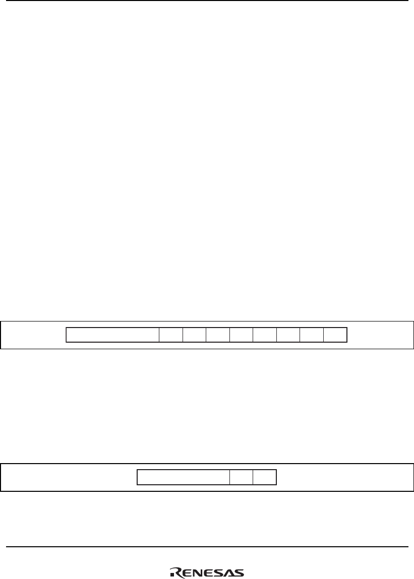
8. Caches
Rev.1.00 Jan. 10, 2008 Page 225 of 1658
REJ09B0261-0100
6. Cache miss (copy-back, with write-back)
The tag and data field of the cache line on the way which is selected to replace are saved in the
write-back buffer. Then a data write in accordance with the access size is performed for the
data field on the hit way which is indexed by virtual address bits [4:0]. Then, the data,
excluding the cache-missed data which is written already, is read into the cache line on the
way which is selected to replace from the physical address space corresponding to the virtual
address. Data reading is performed, using the wraparound method, in order from the quad-
word data (8 bytes) including the cache-missed data. While the remaining data on the cache
line is being read, the CPU can execute the next processing. When reading of one line of data
is completed, the tag corresponding to the physical address is recorded in the cache, 1 is
written to the V bit and the U bit on the way. Then the LRU bit is updated to indicate the way
is latest one. Then the data in the write-back buffer is then written back to external memory.
7. Cache miss (write-through)
A write of the specified access size is performed to the external memory corresponding to the
virtual address. In this case, a write to cache is not performed.
8.3.4 Write-Back Buffer
In order to give priority to data reads to the cache and improve performance, this LSI has a write-
back buffer which holds the relevant cache entry when it becomes necessary to purge a dirty cache
entry into external memory as the result of a cache miss. The write-back buffer contains one cache
line of data and the physical address of the purge destination.
LW7Physical address bits [28:5] LW6LW5LW4LW3LW2LW1LW0
Figure 8.3 Configuration of Write-Back Buffer
8.3.5 Write-Through Buffer
This LSI has a 64-bit buffer for holding write data when writing data in write-through mode or
writing to a non-cacheable area. This allows the CPU to proceed to the next operation as soon as
the write to the write-through buffer is completed, without waiting for completion of the write to
external memory.
Physical address bits[28:0] LW1LW0
Figure 8.4 Configuration of Write-Through Buffer

8. Caches
Rev.1.00 Jan. 10, 2008 Page 226 of 1658
REJ09B0261-0100
8.3.6 OC Two-Way Mode
When the OC2W bit in RAMCR is set to 1, OC two-way mode which only uses way 0 and way 1
in the OC is entered. Thus, power consumption can be reduced. In this mode, only way 0 and way
1 are used even if a memory-mapped OC access is made.
The OC2W bit should be modified by a program in the P2 area. At that time, if the valid line has
already been recorded in the OC, data should be written back by software, if necessary, 1 should
be written to the OCI bit in CCR, and all entries in the OC should be invalid before modifying the
OC2W bit.

8. Caches
Rev.1.00 Jan. 10, 2008 Page 227 of 1658
REJ09B0261-0100
8.4 Instruction Cache Operation
8.4.1 Read Operation
When the IC is enabled (ICE = 1 in CCR) and instruction fetches are performed from a cacheable
area, the instruction cache operates as follows:
1. The tag, V bit, U bit and LRU bits on each way are read from the cache line indexed by virtual
address bits [12:5].
2. The tag, read from each way, is compared with bits [28:10] of the physical address resulting
from virtual address translation by the MMU:
⎯ If there is a way whose tag matches and the V bit is 1, see No. 3.
⎯ If there is no way whose tag matches and the V bit is 1, see No. 4.
3. Cache hit
The data indexed by virtual address bits [4:2] is read as an instruction from the data field on
the hit way. The LRU bits are updated to indicate the way is the latest one.
4. Cache miss
Data is read into the cache line on the way which selected using LRU bits to replace from the
physical address space corresponding to the virtual address. Data reading is performed, using
the wraparound method, in order from the quad-word data (8 bytes) including the cache-
missed data, and when the corresponding data arrives in the cache, the read data is returned to
the CPU as an instruction. While the remaining one cache line of data is being read, the CPU
can execute the next processing. When reading of one line of data is completed, the tag
corresponding to the physical address is recorded in the cache, and 1 is written to the V bit, the
LRU bits are updated to indicate the way is the latest one.
8.4.2 Prefetch Operation
When the IC is enabled (ICE = 1 in CCR) and instruction prefetches are performed from a
cacheable area, the instruction cache operates as follows:
1. The tag, V bit, Ubit and LRU bits on each way are read from the cache line indexed by virtual
address bits [12:5].
2. The tag, read from each way, is compared with bits [28:10] of the physical address resulting
from virtual address translation by the MMU:
⎯ If there is a way whose tag matches and the V bit is 1, see No. 3.
⎯ If there is no way whose tag matches and the V bit is 1, see No. 4.

8. Caches
Rev.1.00 Jan. 10, 2008 Page 228 of 1658
REJ09B0261-0100
3. Cache hit
The LRU bits is updated to indicate the way is the latest one.
4. Cache miss
Data is read into the cache line on a way which selected using the LRU bits to replace from the
physical address space corresponding to the virtual address. Data reading is performed, using
the wraparound method, in order from the quad-word data (8 bytes) including the cache-
missed data. In the prefetch operation, the CPU doesn't wait the data arrived. While the one
cache line of data is being read, the CPU can execute the next processing. When reading of one
line of data is completed, the tag corresponding to the physical address is recorded in the
cache, and 1 is written to the V bit, the LRU bits is updated to indicate the way is the latest
one.
8.4.3 IC Two-Way Mode
When the IC2W bit in RAMCR is set to 1, IC two-way mode which only uses way 0 and way 1 in
the IC is entered. Thus, power consumption can be reduced. In this mode, only way 0 and way 1
are used even if a memory-mapped IC access is made.
The IC2W bit should be modified by a program in the P2 area. At that time, if the valid line has
already been recorded in the IC, 1 should be written to the ICI bit in CCR and all entries in the IC
should be invalid before modifying the IC2W bit.
8.4.4 Instruction Cache Way Prediction Operation
This LSI incorporates an instruction cache (IC) way prediction scheme to reduce power
consumption. This is achieved by activating only the data array that corresponds to a predicted
way. When way prediction misses occur, data must be re-read from the right way, which may lead
to lower performance in instruction fetching. Setting the ICWPD bit to 1 disables the IC way
prediction scheme. Since way prediction misses do not occur in this mode, there is no loss of
performance in instruction fetching but the IC consumes more power. The ICWPD bit should be
modified by a program in the non-cacheable P2 area. If a valid line has already been recorded in
the IC at this time, invalidate all entries in the IC by writing 1 to the ICI bit in CCR before
modifying the ICWPD bit.

8. Caches
Rev.1.00 Jan. 10, 2008 Page 229 of 1658
REJ09B0261-0100
8.5 Cache Operation Instruction
8.5.1 Coherency between Cache and External Memory
(1) Cache Operation Instruction
Coherency between cache and external memory should be assured by software. In this LSI, the
following six instructions are supported for cache operations. Details of these instructions are
given in section 11, Instruction Descriptions of the SH-4A Extended Functions Software Manual.
• Operand cache invalidate instruction: OCBI @Rn
Operand cache invalidation (no write-back)
• Operand cache purge instruction: OCBP @Rn
Operand cache invalidation (with write-back)
• Operand cache write-back instruction: OCBWB @Rn
Operand cache write-back
• Operand cache allocate instruction: MOVCA.L R0,@Rn
Operand cache allocation
• Instruction cache invalidate instruction: ICBI @Rn
Instruction cache invalidation
• Operand access synchronization instruction: SYNCO
Wait for data transfer completion
(2) Coherency Control
The operand cache can receive "PURGE" and "FLUSH" transaction from SuperHyway bus to
control the cache coherency. Since the address used by the PURGE and FLUSH transaction is a
physical address, do not use the 1 Kbyte page size to avoid cache synonym problem in MMU
enable mode.
• PURGE transaction
When the operand cache is enabled, the PURGE transaction checks the operand cache and
invalidates the hit entry. If the invalidated entry is dirty, the data is written back to the external
memory. If the transaction is not hit to the cache, it is no-operation.

8. Caches
Rev.1.00 Jan. 10, 2008 Page 230 of 1658
REJ09B0261-0100
• FLUSH transaction
When the operand cache is enabled, the FLUSH transaction checks the operand cache and if
the hit line is dirty, then the data is written back to the external memory. If the transaction is
not hit to the cache or the hit entry is not dirty, it is no-operation.
(3) Changes in Instruction Specifications Regarding Coherency Control
Of the operand cache operating instructions, the coherency control-related specifications of OCBI,
OCBP, and OCBWB have been changed from those of the SH-4A with H'20-valued VER bits in
the processor version register (PVR).
• Changes in the invalidate instruction OCBI@Rn
When Rn is designating an address in a non-cacheable area, this instruction is executed as
NOP in the SH-4A with H'20-valued VER bits in the processor version register (PVR). In this
LSI, this instruction invalidates the operand cache line designated by way = Rn[14:13] and
entry = Rn[12:5] provided that Rn[31:24] = H'F4 (OC address array area). In this process,
writing back of the line does not take place even if the line to be invalidated is dirty. This
operation is only executable in privileged mode, and an address error exception occurs in user
mode. TLB-related exceptions do not occur.
Do not execute this instruction to invalidate the memory-mapped array areas and control
register areas for which Rn[31:24] is not H'F4, and their reserved areas (H'F0 to H'F3, H'F5 to
H'FF).
• Changes in the purge instruction OCBP@Rn
When Rn is designating an address in a non-cacheable area, this instruction is executed as
NOP in the SH-4A with H'20-valued VER bits in the processor version register (PVR). In this
LSI, this instruction invalidates the operand cache line designated by way = Rn[14:13] and
entry = Rn[12:5] provided that Rn[31:24] = H'F4 (OC address array area). In this process,
writing back of the line takes place when the line to be invalidated is dirty. This operation is
only executable in privileged mode, and an address error exception occurs in user mode. TLB-
related exceptions do not occur.
Do not execute this instruction to invalidate the memory-mapped array areas and control
register areas for which Rn[31:24] is not H'F4, and their reserved areas (H'F0 to H'F3, H'F5 to
H'FF).
• Changes in the write-back instruction OCBWB@Rn
When Rn is designating an address in a non-cacheable area, this instruction is executed as
NOP in the SH-4A with H'20-valued VER bits in the processor version register (PVR). In this
LSI, provided that Rn[31:24] = H'F4 (OC address array area), this instruction writes back the
operand cache line designated by way = Rn[14:13] and entry = Rn[12:5] if it is dirty and clears

8. Caches
Rev.1.00 Jan. 10, 2008 Page 231 of 1658
REJ09B0261-0100
the dirty bit to 0. This operation is only executable in privileged mode, and an address error
exception occurs in user mode. TLB-related exceptions do not occur.
Do not execute this instruction to invalidate the memory-mapped array areas and control
register areas for which Rn[31:24] is not H'F4, and their reserved areas (H'F0 to H'F3, H'F5 to
H'FF).
8.5.2 Prefetch Operation
This LSI supports a prefetch instruction to reduce the cache fill penalty incurred as the result of a
cache miss. If it is known that a cache miss will result from a read or write operation, it is possible
to fill the cache with data beforehand by means of the prefetch instruction to prevent a cache miss
due to the read or write operation, and so improve software performance. If a prefetch instruction
is executed for data already held in the cache, or if the prefetch address results in a UTLB miss or
a protection violation, the result is no operation, and an exception is not generated. Details of the
prefetch instruction are given in section 11, Instruction Descriptions of the SH-4A Extended
Functions Software Manual.
• Prefetch instruction (OC) : PREF @Rn
• Prefetch instruction (IC) : PREFI @Rn

8. Caches
Rev.1.00 Jan. 10, 2008 Page 232 of 1658
REJ09B0261-0100
8.6 Memory-Mapped Cache Configuration
The IC and OC can be managed by software. The contents of IC data array can be read from or
written to by a program in the P2 area by means of a MOV instruction in privileged mode. The
contents of IC address array can also be read from or written to in privileged mode by a program
in the P2 area or the IL memory area by means of a MOV instruction. Operation is not guaranteed
if access is made from a program in another area. In this case, execute one of the following three
methods for executing a branch to the P0, U0, P1, or P3 area.
1. Execute a branch using the RTE instruction.
2. Execute a branch to the P0, U0, P1, or P3 area after executing the ICBI instruction for any
address (including non-cacheable area).
3. If the MC bit in IRMCR is 0 (initial value) before making an access to the memory-mapped
IC, the specific instruction does not need to be executed. However, note that the CPU
processing performance will be lowered because the instruction fetch is performed again for
the next instruction after making an access to the memory-mapped IC.
Note that the method 3 may not be guaranteed in the future SuperH Series. Therefore, it is
recommended that the method 1 or 2 should be used for being compatible with the future SuperH
Series.
In privileged mode, the OC contents can be read from or written to by a program in the P1 or P2
area by means of a MOV instruction. Operation is not guaranteed if access is made from a
program in another area. The IC and OC are allocated to the P4 area in the virtual address space.
Only data accesses can be used on both the IC address array and data array and the OC address
array and data array, and accesses are always longword-size. Instruction fetches cannot be
performed in these areas. For reserved bits, a write value of 0 should be specified and the read
value is undefined.
8.6.1 IC Address Array
The IC address array is allocated to addresses H'F000 0000 to H'F0FF FFFF in the P4 area. An
address array access requires a 32-bit address field specification (when reading or writing) and a
32-bit data field specification. The way and entry to be accessed are specified in the address field,
and the write tag and V bit are specified in the data field.
In the address field, bits [31:24] have the value H'F0 indicating the IC address array, and the way
is specified by bits [14:13] and the entry by bits [12:5]. The association bit (A bit) [3] in the
address field specifies whether or not association is performed when writing to the IC address
array. As only longword access is used, 0 should be specified for address field bits [1:0].
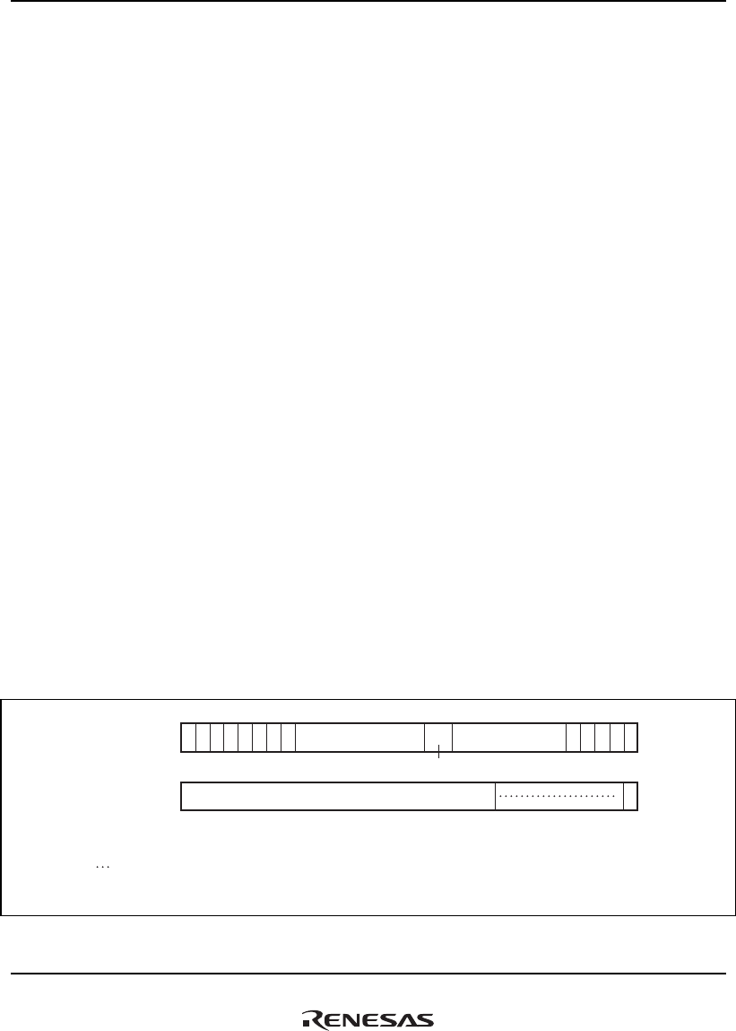
8. Caches
Rev.1.00 Jan. 10, 2008 Page 233 of 1658
REJ09B0261-0100
In the data field, the tag is indicated by bits [31:10], and the V bit by bit [0]. As the IC address
array tag is 19 bits in length, data field bits [31:29] are not used in the case of a write in which
association is not performed. Data field bits [31:29] are used for the virtual address specification
only in the case of a write in which association is performed.
The following three kinds of operation can be used on the IC address array:
1. IC address array read
The tag and V bit are read into the data field from the IC entry corresponding to the way and
entry set in the address field. In a read, associative operation is not performed regardless of
whether the association bit specified in the address field is 1 or 0.
2. IC address array write (non-associative)
The tag and V bit specified in the data field are written to the IC entry corresponding to the
way and entry set in the address field. The A bit in the address field should be cleared to 0.
3. IC address array write (associative)
When a write is performed with the A bit in the address field set to 1, the tag in each way
stored in the entry specified in the address field is compared with the tag specified in the data
field. The way numbers of bits [14:13] in the address field are not used. If the MMU is enabled
at this time, comparison is performed after the virtual address specified by data field bits
[31:10] has been translated to a physical address using the ITLB. If the addresses match and
the V bit in the way is 1, the V bit specified in the data field is written into the IC entry. In
other cases, no operation is performed. This operation is used to invalidate a specific IC entry.
If an ITLB miss occurs during address translation, or the comparison shows a mismatch, an
exception is not generated, no operation is performed, and the write is not executed.
Note: IC address array associative writing function may not be supported in the future SuperH
Series. Therefore, it is recommended that the ICBI instruction should be used to operate
the IC definitely by handling ITLB miss and reporting ITLB miss exception.
Address field
31 23 12 543210
11110000 0000
Entry
A
Data field
31 10 9 1 0
V
Tag
Way
V
A
24 1314
15
: Validity bit
: Association bit
:
Reserved bits
(write value should be 0 and read value is undefined )
: Don't care
*
*********
Figure 8.5 Memory-Mapped IC Address Array (Cache size = 32 Kbytes)
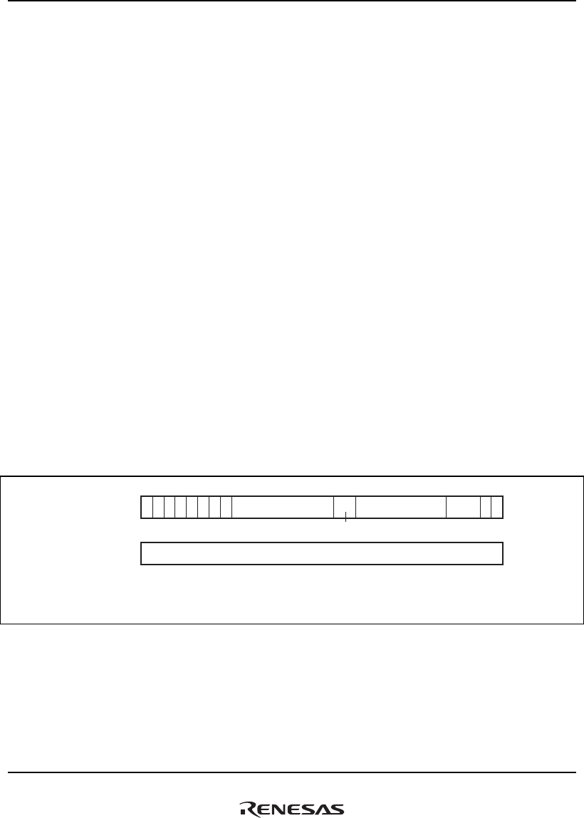
8. Caches
Rev.1.00 Jan. 10, 2008 Page 234 of 1658
REJ09B0261-0100
8.6.2 IC Data Array
The IC data array is allocated to addresses H'F100 0000 to H'F1FF FFFF in the P4 area. A data
array access requires a 32-bit address field specification (when reading or writing) and a 32-bit
data field specification. The way and entry to be accessed are specified in the address field, and
the longword data to be written is specified in the data field.
In the address field, bits [31:24] have the value H'F1 indicating the IC data array, and the way is
specified by bits [14:13] and the entry by bits [12:5]. Address field bits [4:2] are used for the
longword data specification in the entry. As only longword access is used, 0 should be specified
for address field bits [1:0].
The data field is used for the longword data specification.
The following two kinds of operation can be used on the IC data array:
1. IC data array read
Longword data is read into the data field from the data specified by the longword specification
bits in the address field in the IC entry corresponding to the way and entry set in the address
field.
2. IC data array write
The longword data specified in the data field is written for the data specified by the longword
specification bits in the address field in the IC entry corresponding to the way and entry set in
the address field.
Address field
31 23 12 5 4 2 1 0
11110001 Entry L
Data field
31 0
Longword data
L
*
24 131415
: Longword specification bits
: Don't care
Way
00
*********
Figure 8.6 Memory-Mapped IC Data Array (Cache size = 32 Kbytes)
8.6.3 OC Address Array
The OC address array is allocated to addresses H'F400 0000 to H'F4FF FFFF in the P4 area. An
address array access requires a 32-bit address field specification (when reading or writing) and a

8. Caches
Rev.1.00 Jan. 10, 2008 Page 235 of 1658
REJ09B0261-0100
32-bit data field specification. The way and entry to be accessed are specified in the address field,
and the write tag, U bit, and V bit are specified in the data field.
In the address field, bits [31:24] have the value H'F4 indicating the OC address array, and the way
is specified by bits [14:13] and the entry by bits [12:5]. The association bit (A bit) [3] in the
address field specifies whether or not association is performed when writing to the OC address
array. As only longword access is used, 0 should be specified for address field bits [1:0].
In the data field, the tag is indicated by bits [31:10], the U bit by bit [1], and the V bit by bit [0].
As the OC address array tag is 19 bits in length, data field bits [31:29] are not used in the case of a
write in which association is not performed. Data field bits [31:29] are used for the virtual address
specification only in the case of a write in which association is performed.
The following three kinds of operation can be used on the OC address array:
1. OC address array read
The tag, U bit, and V bit are read into the data field from the OC entry corresponding to the
way and entry set in the address field. In a read, associative operation is not performed
regardless of whether the association bit specified in the address field is 1 or 0.
2. OC address array write (non-associative)
The tag, U bit, and V bit specified in the data field are written to the OC entry corresponding to
the way and entry set in the address field. The A bit in the address field should be cleared to 0.
When a write is performed to a cache line for which the U bit and V bit are both 1, after write-
back of that cache line, the tag, U bit, and V bit specified in the data field are written.
3. OC address array write (associative)
When a write is performed with the A bit in the address field set to 1, the tag in each way
stored in the entry specified in the address field is compared with the tag specified in the data
field. The way numbers of bits [14:13] in the address field are not used. If the MMU is enabled
at this time, comparison is performed after the virtual address specified by data field bits
[31:10] has been translated to a physical address using the UTLB. If the addresses match and
the V bit in the way is 1, the U bit and V bit specified in the data field are written into the OC
entry. In other cases, no operation is performed. This operation is used to invalidate a specific
OC entry. If the OC entry U bit is 1, and 0 is written to the V bit or to the U bit, write-back is
performed. If a UTLB miss occurs during address translation, or the comparison shows a
mismatch, an exception is not generated, no operation is performed, and the write is not
executed.
Note: OC address array associative writing function may not be supported in the future SuperH
Series. Therefore, it is recommended that the OCBI, OCBP, or OCBWB instruction
should be used to operate the OC definitely by reporting data TLB miss exception.
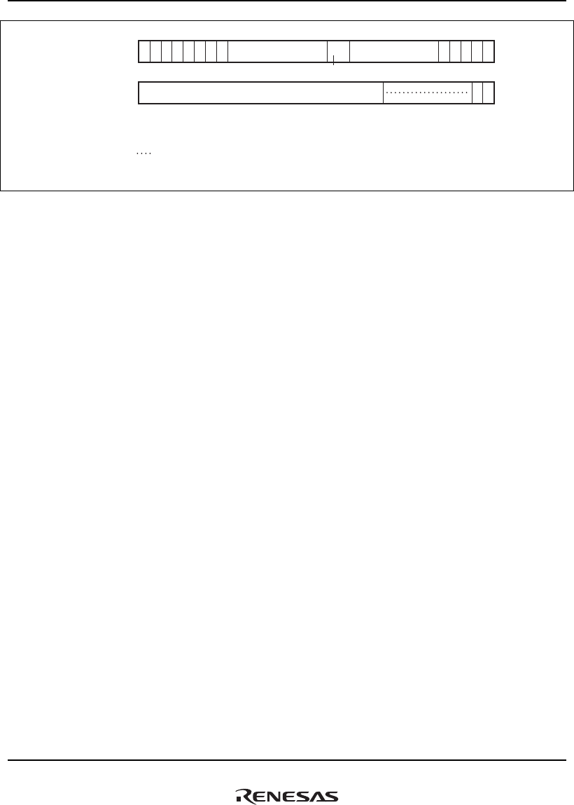
8. Caches
Rev.1.00 Jan. 10, 2008 Page 236 of 1658
REJ09B0261-0100
Address field
31 23 543210
1 1 1 1 0 1 0 0 Entry A
Data field
31 10 9 1 0
V
Tag
24 13121415
2
U
V
U
A
: Validity bit
: Dirty bit
: Association bit
:
Reserved bits
(write value should be 0 and read value is undefined )
: Don't care
Way
0000
*********
*
Figure 8.7 Memory-Mapped OC Address Array (Cache size = 32 Kbytes)
8.6.4 OC Data Array
The OC data array is allocated to addresses H'F500 0000 to H'F5FF FFFF in the P4 area. A data
array access requires a 32-bit address field specification (when reading or writing) and a 32-bit
data field specification. The way and entry to be accessed are specified in the address field, and
the longword data to be written is specified in the data field.
In the address field, bits [31:24] have the value H'F5 indicating the OC data array, and the way is
specified by bits [14:13] and the entry by bits [12:5]. Address field bits [4:2] are used for the
longword data specification in the entry. As only longword access is used, 0 should be specified
for address field bits [1:0].
The data field is used for the longword data specification.
The following two kinds of operation can be used on the OC data array:
1. OC data array read
Longword data is read into the data field from the data specified by the longword specification
bits in the address field in the OC entry corresponding to the way and entry set in the address
field.
2. OC data array write
The longword data specified in the data field is written for the data specified by the longword
specification bits in the address field in the OC entry corresponding to the way and entry set in
the address field. This write does not set the U bit to 1 on the address array side.

8. Caches
Rev.1.00 Jan. 10, 2008 Page 237 of 1658
REJ09B0261-0100
Address field
31 23 543210
11110101 Entry
Data field
31 0
Longword data
24 13121415
L
*
: Longword specification bits
: Don't care
Way
0L0
*********
Figure 8.8 Memory-Mapped OC Data Array (Cache size = 32 Kbytes)
8.6.5 Memory-Mapped Cache Associative Write Operation
Associative writing to the IC and OC address arrays may not be supported in future SuperH-
family products. The use of instructions ICBI, OCBI, OCBP, and OCBWB is recommended.
These instructions handle ITLB misses, and notify instruction TLB miss exceptions and data TLB
miss exceptions, thus providing a sure way of controlling the IC and OC. As a transitional
measure, this LSI generates address errors when this function is used. If compatibility with
previous products is a crucial consideration, on the other hand, the MMCAW bit in EXPMASK
(H'FF2F 0004) can be set to 1 to enable this function. However, instructions ICBI, OCBI, OCBP,
and OCBWB should be used to guarantee compatibility with future SuperH-family products.
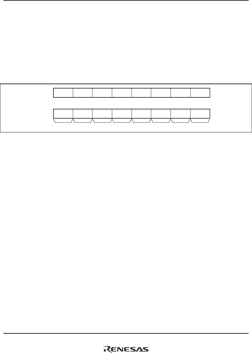
8. Caches
Rev.1.00 Jan. 10, 2008 Page 238 of 1658
REJ09B0261-0100
8.7 Store Queues
This LSI supports two 32-byte store queues (SQs) to perform high-speed writes to external
memory.
8.7.1 SQ Configuration
There are two 32-byte store queues, SQ0 and SQ1, as shown in figure 8.9. These two store queues
can be set independently.
SQ0 SQ0[0] SQ0[1] SQ0[2] SQ0[3] SQ0[4] SQ0[5] SQ0[6] SQ0[7]
SQ1 SQ1[0] SQ1[1] SQ1[2] SQ1[3] SQ1[4] SQ1[5] SQ1[6] SQ1[7]
4 byte 4 byte 4 byte 4 byte 4 byte 4 byte 4 byte 4 byte
Figure 8.9 Store Queue Configuration
8.7.2 Writing to SQ
A write to the SQs can be performed using a store instruction for addresses H'E000 0000 to
H'E3FF FFFC in the P4 area. A longword or quadword access size can be used. The meanings of
the address bits are as follows:
[31:26] : 111000 Store queue specification
[25:6] : Don't care Used for external memory transfer/access right
[5] : 0/1 0: SQ0 specification
1: SQ1 specification
[4:2] : LW specification Specifies longword position in SQ0/SQ1
[1:0] : 00 Fixed at 0

8. Caches
Rev.1.00 Jan. 10, 2008 Page 239 of 1658
REJ09B0261-0100
8.7.3 Transfer to External Memory
Transfer from the SQs to external memory can be performed with a prefetch instruction (PREF).
Issuing a PREF instruction for addresses H'E000 0000 to H'E3FF FFFC in the P4 area starts a
transfer from the SQs to external memory. The transfer length is fixed at 32 bytes, and the start
address is always at a 32-byte boundary. While the contents of one SQ are being transferred to
external memory, the other SQ can be written to without a penalty cycle. However, writing to the
SQ involved in the transfer to external memory is kept waiting until the transfer is completed.
The physical address bits [28:0] of the SQ transfer destination are specified as shown below,
according to whether the MMU is enabled or disabled.
• When MMU is enabled (AT = 1 in MMUCR)
The SQ area (H'E000 0000 to H'E3FF FFFF) is set in VPN of the UTLB, and the transfer
destination physical address in PPN. The ASID, V, SZ, SH, PR, and D bits have the same
meaning as for normal address translation, but the C and WT bits have no meaning with regard
to this page. When a prefetch instruction is issued for the SQ area, address translation is
performed and physical address bits [28:10] are generated in accordance with the SZ bit
specification. For physical address bits [9:5], the address prior to address translation is
generated in the same way as when the MMU is disabled. Physical address bits [4:0] are fixed
at 0. Transfer from the SQs to external memory is performed to this address.
• When MMU is disabled (AT = 0 in MMUCR)
The SQ area (H'E000 0000 to H'E3FF FFFF) is specified as the address at which a PREF
instruction is issued. The meanings of address bits [31:0] are as follows:
[31:26] : 111000 Store queue specification
[25:6] : Address Transfer destination physical address bits [25:6]
[5] : 0/1 0: SQ0 specification
1: SQ1 specification and transfer destination physical
address bit [5]
[4:2] : Don't care No meaning in a prefetch
[1:0] : 00 Fixed at 0
Physical address bits [28:26], which cannot be generated from the above address, are generated
from QACR0 and QACR1.
QACR0[4:2] : Physical address bits [28:26] corresponding to SQ0
QACR1[4:2] : Physical address bits [28:26] corresponding to SQ1

8. Caches
Rev.1.00 Jan. 10, 2008 Page 240 of 1658
REJ09B0261-0100
Physical address bits [4:0] are always fixed at 0 since burst transfer starts at a 32-byte
boundary.
8.7.4 Determination of SQ Access Exception
Determination of an exception in a write to an SQ or transfer to external memory (PREF
instruction) is performed as follows according to whether the MMU is enabled or disabled. If an
exception occurs during a write to an SQ, the SQ contents before the write are retained. If an
exception occurs in a data transfer from an SQ to external memory, the transfer to external
memory will be aborted.
• When MMU is enabled (AT = 1 in MMUCR)
Operation is in accordance with the address translation information recorded in the UTLB, and
the SQMD bit in MMUCR. Write type exception judgment is performed for writes to the SQs,
and read type exception judgment for transfer from the SQs to external memory (using a PREF
instruction). As a result, a TLB miss exception or protection violation exception is generated
as required. However, if SQ access is enabled in privileged mode only by the SQMD bit in
MMUCR, an address error will occur even if address translation is successful in user mode.
• When MMU is disabled (AT = 0 in MMUCR)
Operation is in accordance with the SQMD bit in MMUCR.
0: Privileged/user mode access possible
1: Privileged mode access possible
If the SQ area is accessed in user mode when the SQMD bit in MMUCR is set to 1, an address
error will occur.
8.7.5 Reading from SQ
In privileged mode in this LSI, reading the contents of the SQs may be performed by means of a
load instruction for addresses H'FF00 1000 to H'FF00 103C in the P4 area. Only longword access
is possible.
[31:6] : H'FF00 1000 Store queue specification
[5] : 0/1 0: SQ0 specification
1: SQ1 specification
[4:2] : LW specification Specifies longword position in SQ0/SQ1
[1:0] : 00 Fixed at 0

8. Caches
Rev.1.00 Jan. 10, 2008 Page 241 of 1658
REJ09B0261-0100
8.8 Notes on Using 32-Bit Address Extended Mode
In 32-bit address extended mode, the items described in this section are extended as follows.
1. The tag bits [28:10] (19 bits) in the IC and OC are extended to bits [31:10] (22 bits).
2. An instruction which operates the IC (a memory-mapped IC access and writing to the ICI bit
in CCR) should be located in the P1 or P2 area. The cacheable bit (C bit) in the corresponding
entry in the PMB should be 0.
3. Bits [4:2] (3 bits) for the AREA0 bit in QACR0 and the AREA1 bit in QACR1 are extended to
bits [7:2] (6 bits).

8. Caches
Rev.1.00 Jan. 10, 2008 Page 242 of 1658
REJ09B0261-0100

9. On-Chip Memory
Rev.1.00 Jan. 10, 2008 Page 243 of 1658
REJ09B0261-0100
Section 9 On-Chip Memory
This LSI includes three types of memory modules for storage of instructions and data: OL
memory, IL memory, and U memory. The OL memory is suitable for data storage while the IL
memory is suitable for instruction storage. The U memory can store instructions and/or data.
9.1 Features
(1) OL Memory
• Capacity
The OL memory in this LSI is 16 Kbytes.
• Page
The OL memory is divided into four pages (pages 0A, 0B, 1A and 1B).
• Memory map
The OL memory is allocated in the addresses shown in table 9.1 in both the virtual address
space and the physical address space.
Table 9.1 OL memory Addresses
Page 0A H'E500 E000 to H'E500 EFFF
Page 0B H'E500 F000 to H'E500 FFFF
Page 1A H'E501 0000 to H'E501 0FFF
Page 1B H'E501 1000 to H'E501 1FFF
• Ports
Each page has three independent read/write ports and is connected to the SuperHyway bus, the
cache/RAM internal bus, and operand bus. The operand bus is used when the OL memory is
accessed through operand access. The cache/RAM internal bus is used when the OL memory
is accessed through instruction fetch. The SuperHyway bus is used for OL memory access
from the SuperHyway bus master module.
• Priority
In the event of simultaneous accesses to the same page from different buses, the access
requests are processed according to priority. The priority order is: SuperHyway bus >
Cache/RAM internal bus > operand bus.

9. On-Chip Memory
Rev.1.00 Jan. 10, 2008 Page 244 of 1658
REJ09B0261-0100
(2) IL Memory
• Capacity
The IL memory in this LSI is 8 Kbytes.
• Page
The IL memory is divided into two pages (pages 0 and 1).
• Memory map
The IL memory is allocated to the addresses shown in table 9.2 in both the virtual address
space and the physical address space.
Table 9.2 IL Memory Addresses
Page Memory Address
Page 0 H'E520 0000 to H'E520 0FFF
Page 1 ⎯
• Ports
The page has three independent read/write ports and is connected to the SuperHyway bus, the
cache/RAM internal bus, and the instruction bus. The instruction bus is used when the IL
memory is accessed through instruction fetch. The cache/RAM internal bus is used when the
IL memory is accessed through operand access. The SuperHyway bus is used for IL memory
access from the SuperHyway bus master module.
• Priority
In the event of simultaneous accesses to the same page from different buses, the access
requests are processed according to priority. The priority order is: SuperHyway bus >
cache/RAM internal bus > instruction bus.
(3) U Memory
• Capacity
The U memory in this LSI is 128 Kbytes.
• Access method
Instruction fetch and operand write access are performed via the cache/RAM internal bus.
Operand read access is optimized for sequential operand access by using the read buffer.
• Memory map
The U memory is allocated to the addresses shown in table 9.3 in both the virtual address
space and the physical address space.

9. On-Chip Memory
Rev.1.00 Jan. 10, 2008 Page 245 of 1658
REJ09B0261-0100
The CPU can access the P4 area in the virtual address space (when SR.MD = 1) or on-chip
memory area (when SR.MD = 0 and RAMCR.RMD = 1). Access operations involving these
addresses are always non-cacheable.
Table 9.3 U Memory Addresses
Address Space Memory Address
Virtual address H'E55F 0000 to H'E560 FFFF
Physical address H'E55F 0000 to H'E560 FFFF
• Ports
The U memory has three independent read/write ports and is connected to the operand bus, the
cache/RAM internal bus, and the SuperHyway bus. The operand bus is used when the U
memory is accessed through operand read access. The cache/RAM internal bus is used when
the U memory is accessed through instruction fetch and operand write access. The
SuperHyway bus is used for U memory access from the SuperHyway bus master module.
• Priority
In the event of simultaneous accesses to the U memory from different buses, the access
requests are processed according to priority. The priority order is: SuperHyway bus >
cache/RAM internal bus > operand bus.

9. On-Chip Memory
Rev.1.00 Jan. 10, 2008 Page 246 of 1658
REJ09B0261-0100
9.2 Register Descriptions
The following registers are related to the on-chip memory.
Table 9.4 Register Configuration
Name Abbreviation R/W P4 Address*
Area 7
Address* Access Size
On-chip memory control
register
RAMCR R/W H'FF00 0074 H'1F00 0074 32
OL memory transfer source
address register 0
LSA0 R/W H'FF00 0050 H'1F00 0050 32
OL memory transfer source
address register 1
LSA1 R/W H'FF00 0054 H'1F00 0054 32
OL memory transfer
destination address register
0
LDA0 R/W H'FF00 0058 H'1F00 0058 32
OL memory transfer
destination address register
1
LDA1 R/W H'FF00 005C H'1F00 005C 32
Note: * The P4 address is the address used when using P4 area in the virtual address space.
The area 7 address is the address used when accessing from area 7 in the physical
address space using the TLB.
Table 9.5 Register States in Each Processing Mode
Name Abbreviation
Power-On
Reset Manual Reset Sleep Standby
On-chip memory control
register
RAMCR H'0000 0000 H'0000 0000 Retained Retained
OL memory transfer source
address register 0
LSA0 Undefined Undefined Retained Retained
OL memory transfer source
address register 1
LSA1 Undefined Undefined Retained Retained
OL memory transfer
destination address register
0
LDA0 Undefined Undefined Retained Retained
OL memory transfer
destination address register
1
LDA1 Undefined Undefined Retained Retained

9. On-Chip Memory
Rev.1.00 Jan. 10, 2008 Page 247 of 1658
REJ09B0261-0100
9.2.1 On-Chip Memory Control Register (RAMCR)
RAMCR controls the protective functions in the on-chip memory.
When updating RAMCR, please follow limitation described at section 8.2.4, On-Chip Memory
Control Register (RAMCR).
31 30 29 28 27 26 25 24 23 22 21 20 19 18 17 16
Bit :
0000000000000000
RMD RP IC2W
OC2W
Initial value :
RRRRRRRRRRRRRRRR
R/W:
15 14 13 12 11 10 9 8 7 6 5 4 3 2 1 0
Bit :
0000000000000000
Initial value :
R R R R R R R/W R/W R/W R/W R/W R R R R R
R/W:
ICWPD
Bit Bit Name
Initial
Value R/W Description
31to10 — All 0 R Reserved
For read/write in these bits, refer to General
Precautions on Handling of Product.
9 RMD 0 R/W On-Chip Memory Access Mode
Specifies the right of access to the on-chip memory
from the virtual address space.
0: An access in privileged mode is allowed.
(An address error exception occurs in user mode.)
1: An access in user/ privileged mode is allowed.
8 RP 0 R/W On-Chip Memory Protection Enable
Selects whether or not to use the protective functions
using ITLB and UTLB for accessing the on-chip
memory from the virtual address space.
0: Protective functions are not used.
1: Protective functions are used.
For further details, refer to section 9.4, On-Chip
Memory Protective Functions.
7 IC2W 0 R/W IC Two-Way Mode
For further details, refer to section 8.4.3, IC Two-Way
Mode.
9. On-Chip Memory
Rev.1.00 Jan. 10, 2008 Page 248 of 1658
REJ09B0261-0100
Bit Bit Name
Initial
Value R/W Description
6 OC2W 0 R/W OC Two-Way Mode
For further details, refer to section 8.3.6, OC Two-Way
Mode.
5 ICWPD 0 R/W IC Way Prediction Disable
For further details, refer to section 8.4.4, Instruction
Cache Way Prediction Operation.
4 to 0 — All 0 R Reserved
For read/write in these bits, refer to General
Precautions on Handling of Product.
9.2.2 OL memory Transfer Source Address Register 0 (LSA0)
When MMUCR.AT = 0 or RAMCR.RP = 0, the LSA0 specifies the transfer source physical
address for block transfer to page 0A or 0B of the OL memory.
31 30 29 28 27 26 25 24 23 22 21 20 19 18 17 16
Bit :
000
Initial value :
R R R R/W R/W R/W R/W R/W R/W R/W
L0DADR
L0DADR L0DSZ
R/W R/W R/W R/W R/W R/W
R/W:
1514131211109876543210
Bit :
0000
Initial value :
R/WR/WR/WR/WR/WR/WRRRRR/WR/WR/WR/WR/WR/W
R/W:
Bit Bit Name
Initial
Value R/W Description
31 to 29 — All 0 R Reserved
For read/write in these bits, refer General Precautions
on Handling of Product.
28 to 10 L0SADR Undefined R/W OL memory Page 0 Block Transfer Source Address
When MMUCR.AT = 0 or RAMCR.RP = 0, these bits
specify the transfer source physical address for block
transfer to page 0A or 0B in the OL memory.
9 to 6 — All 0 R Reserved
For read/write in these bits, refer to General
Precautions on Handling of Product.

9. On-Chip Memory
Rev.1.00 Jan. 10, 2008 Page 249 of 1658
REJ09B0261-0100
Bit Bit Name
Initial
Value R/W Description
5 to 0 L0SSZ Undefined R/W OL memory Page 0 Block Transfer Source Address
Select
When MMUCR.AT = 0 or RAMCR.RP = 0, these bits
select whether the operand addresses or L0SADR
values are used as bits 15 to 10 of the transfer source
physical address for block transfer to page 0A or 0B in
the OL memory. L0SSZ[5:0] correspond to the transfer
source physical addresses [15:10].
0: The operand address is used as the transfer source
physical address.
1: The L0SADR value is used as the transfer source
physical address.
Settable values:
111111: Transfer source physical address is specified
in 1-Kbyte units.
111110: Transfer source physical address is specified
in 2-Kbyte units.
111100: Transfer source physical address is specified
in 4-Kbyte units.
111000: Transfer source physical address is specified
in 8-Kbyte units.
110000: Transfer source physical address is specified
in 16-Kbyte units.
100000: Transfer source physical address is specified
in 32-Kbyte units.
000000: Transfer source physical address is specified
in 64-Kbyte units.
Settings other than the ones given above are
prohibited.

9. On-Chip Memory
Rev.1.00 Jan. 10, 2008 Page 250 of 1658
REJ09B0261-0100
9.2.3 OL memory Transfer Source Address Register 1 (LSA1)
When MMUCR.AT = 0 or RAMCR.RP = 0, the LSA1 specifies the transfer source physical
address for block transfer to page 1A or 1B in the OL memory.
31 30 29 28 27 26 25 24 23 22 21 20 19 18 17 16
Bit :
000
Initial value :
R R R R/W R/W R/W R/W R/W R/W R/W
L1SADR
L1SADR L1SSZ
R/W R/W R/W R/W R/W R/W
R/W:
15 14 13 12 11 10 9 8 7 6 5 4 3 2 1 0
Bit :
0000
Initial value :
R/W R/W R/W R/W R/W R/W R R R R R/W R/W R/W R/W R/W R/W
R/W:
Bit Bit Name
Initial
Value R/W Description
31 to 29 — All 0 R Reserved
For read/write in these bits, refer to General
Precautions on Handling of Product.
28 to 10 L1SADR Undefined R/W OL memory Page 1 Block Transfer Source Address
When MMUCR.AT = 0 or RAMCR.RP = 0, these bits
specify transfer source physical address for block
transfer to page 1A or 1B in the OL memory.
9 to 6 — All 0 R Reserved
For read/write in these bits, refer to General
Precautions on Handling of Product.

9. On-Chip Memory
Rev.1.00 Jan. 10, 2008 Page 251 of 1658
REJ09B0261-0100
Bit Bit Name
Initial
Value R/W Description
5 to 0 L1SSZ Undefined R/W OL memory Page 1 Block Transfer Source Address
Select
When MMUCR.AT = 0 or RAMCR.RP = 0, these bits
select whether the operand addresses or L1SADR
values are used as bits 15 to 10 of the transfer source
physical address for block transfer to page 1A or 1B in
the OL memory. L1SSZ bits [5:0] correspond to the
transfer source physical addresses [15:10].
0: The operand address is used as the transfer source
physical address.
1: The L1SADR value is used as the transfer source
physical address.
Settable values:
111111: Transfer source physical address is specified
in 1-Kbyte units.
111110: Transfer source physical address is specified
in 2-Kbyte units.
111100: Transfer source physical address is specified
in 4-Kbyte units.
111000: Transfer source physical address is specified
in 8-Kbyte units.
110000: Transfer source physical address is specified
in 16-Kbyte units.
100000: Transfer source physical address is specified
in 32-Kbyte units.
000000: Transfer source physical address is specified
in 64-Kbyte units.
Settings other than the ones given above are
prohibited.

9. On-Chip Memory
Rev.1.00 Jan. 10, 2008 Page 252 of 1658
REJ09B0261-0100
9.2.4 OL memory Transfer Destination Address Register 0 (LDA0)
When MMUCR.AT = 0 or RAMCR.RP = 0, LDA0 specifies the transfer destination physical
address for block transfer to page 0A or 0B of the OL memory.
31 30 29 28 27 26 25 24 23 22 21 20 19 18 17 16
Bit :
000
Initial value :
R R R R/W R/W R/W R/W R/W R/W R/W
L0DADR
L0DADR L0DSZ
R/W R/W R/W R/W R/W R/W
R/W:
1514131211109876543210
Bit :
0000
Initial value :
R/WR/WR/WR/WR/WR/WRRRRR/WR/WR/WR/WR/WR/W
R/W:
Bit Bit Name
Initial
Value R/W Description
31 to 29 — All 0 R Reserved
For read/write in these bits, refer to General
Precautions on Handling of Product.
28 to 10 L0DADR Undefined R/W OL memory Page 0 Block Transfer Destination Address
When MMUCR.AT = 0 or RAMCR.RP = 0, these bits
specify transfer destination physical address for block
transfer to page 0A or 0B in the OL memory.
9 to 6 — All 0 R Reserved
For read/write in these bits, refer to General
Precautions on Handling of Product.

9. On-Chip Memory
Rev.1.00 Jan. 10, 2008 Page 253 of 1658
REJ09B0261-0100
Bit Bit Name
Initial
Value R/W Description
5 to 0 L0DSZ Undefined R/W OL memory Page 0 Block Transfer Destination Address
Select
When MMUCR.AT = 0 or RAMCR.RP = 0, these bits
select whether the operand addresses or L0DADR
values are used as bits 15 to 10 of the transfer
destination physical address for block transfer to page
0A or 0B in the OL memory. L0DSZ bits [5:0]
correspond to the transfer destination physical address
bits [15:10].
0: The operand address is used as the transfer
destination physical address.
1: The L0DADR value is used as the transfer
destination physical address.
Settable values:
111111: Transfer destination physical address is
specified in 1-Kbyte units.
111110: Transfer destination physical address is
specified in 2-Kbyte units.
111100: Transfer destination physical address is
specified in 4-Kbyte units.
111000: Transfer destination physical address is
specified in 8-Kbyte units.
110000: Transfer destination physical address is
specified in 16-Kbyte units.
100000: Transfer destination physical address is
specified in 32-Kbyte units.
000000: Transfer destination physical address is
specified in 64-Kbyte units.
Settings other than the ones given above are
prohibited.

9. On-Chip Memory
Rev.1.00 Jan. 10, 2008 Page 254 of 1658
REJ09B0261-0100
9.2.5 OL memory Transfer Destination Address Register 1 (LDA1)
When MMUCR.AT = 0 or RAMCR.RP = 0, LDA1 specifies the transfer destination physical
address for block transfer to page 1A or 1B in the OL memory.
31 30 29 28 27 26 25 24 23 22 21 20 19 18 17 16
Bit :
000
Initial value :
R R R R/W R/W R/W R/W R/W R/W R/W
L1DADR
L1DADR L1DSZ
R/W R/W R/W R/W R/W R/W
R/W:
1514131211109876543210
Bit :
0000
Initial value :
R/W R/W R/W R/W R/W R/W R R R R R/W R/W R/W R/W R/W R/W
R/W:
Bit Bit Name
Initial
Value R/W Description
31 to 29 — All 0 R Reserved
For read/write in these bits, refer to General
Precautions on Handling of Product.
28 to 10 L1DADR Undefined R/W OL memory Page 1 Block Transfer Destination Address
When MMUCR.AT = 0 or RAMCR.RP = 0, these bits
specify transfer destination physical address for block
transfer to page 1A or 1B in the OL memory.
9 to 6 — All 0 R Reserved
For read/write in these bits, refer to General
Precautions on Handling of Product.

9. On-Chip Memory
Rev.1.00 Jan. 10, 2008 Page 255 of 1658
REJ09B0261-0100
Bit Bit Name
Initial
Value R/W Description
5 to 0 L1DSZ Undefined R/W OL memory Page 1 Block Transfer Destination Address
Select
When MMUCR.AT = 0 or RAMCR.RP = 0, these bits
select whether the operand addresses or L1DADR
values are used as bits 15 to 10 of the transfer
destination physical address for block transfer to page
1A or 1B in the OL memory. L1DSZ bits [5:0]
correspond to the transfer destination physical
addresses [15:10].
0: The operand address is used as the transfer
destination physical address.
1: The L1DADR value is used as the transfer
destination physical address.
Settable values:
111111: Transfer destination physical address is
specified in 1-Kbyte units.
111110: Transfer destination physical address is
specified in 2-Kbyte units.
111100: Transfer destination physical address is
specified in 4-Kbyte units.
111000: Transfer destination physical address is
specified in 8-Kbyte units.
110000: Transfer destination physical address is
specified in 16-Kbyte units.
100000: Transfer destination physical address is
specified in 32-Kbyte units.
000000: Transfer destination physical address is
specified in 64-Kbyte units.
Settings other than the ones given above are
prohibited.

9. On-Chip Memory
Rev.1.00 Jan. 10, 2008 Page 256 of 1658
REJ09B0261-0100
9.3 Operation
9.3.1 Instruction Fetch Access from the CPU
(1) OL Memory
Instruction fetch access from the CPU is performed via the cache/RAM internal bus. This access
takes more than one cycle.
(2) IL Memory
Instruction fetch access from the CPU is performed directly via the instruction bus for a given
virtual address. In the case of successive accesses to the same page of IL memory and as long as
no page conflict occurs, the access takes one cycle.
(3) U Memory
Instruction fetch access from the CPU is performed via the cache/RAM internal bus, and one
instruction fetch takes more than one cycle.
9.3.2 Operand Access from the CPU and Access from the FPU
Note: Operand access is applied for PC relative access (@(disp,pc)).
(1) OL Memory
Access from the CPU or FPU is performed via the operand bus for a given virtual address. Read
access from the operand bus by virtual address takes one cycle if the access is made successively
to the same page of OL memory and as long as no page conflict occurs. Write access from the
operand bus by virtual address takes one cycle as long as no page conflict occurs.
(2) IL Memory
Operand access from the CPU and access from the FPU are performed via the cache/RAM internal
bus. Access via the cache/RAM internal bus takes more than one cycle.

9. On-Chip Memory
Rev.1.00 Jan. 10, 2008 Page 257 of 1658
REJ09B0261-0100
(3) U Memory
Operand access from the CPU and read access from the FPU are performed via the read buffer.
The read buffer is configured with two sets of one-line 32-byte buffers, and holds up to two lines
which have been accessed through operand access by the CPU and accessed through read access
by the FPU. The U memory can be accessed in one cycle when the read buffer is hit. If the read
buffer is missed, 32-byte data including data required from the U memory is read out, and returned
to the CPU, and the read buffer is updated. Access in this case takes more than one cycle. The
LRU algorithm is used to determine which of the two read buffers to update. In write access, the U
memory is directly updated, and if the corresponding line is held in the read buffer, the read buffer
is invalidated. It is unnecessary to guarantee the coherency by software since the hardware
invalidates the read buffer even when the SuperHyway bus master module, such as DMAC,
rewrites the U memory.
9.3.3 Access from the SuperHyway Bus Master Module
On-chip memory is always accessed by the SuperHyway bus master module, such as DMAC, via
the SuperHyway bus which is a physical address bus. The same addresses as for the virtual
addresses must be used.
9.3.4 OL Memory Block Transfer
High-speed data transfer can be performed through block transfer between the OL memory and
external memory without cache utilization.
Data can be transferred from the external memory to the OL memory through a prefetch
instruction (PREF). Block transfer from the external memory to the OL memory begins when the
PREF instruction is issued to the address in the OL memory area in the virtual address space.
Data can be transferred from the OL memory to the external memory through a write-back
instruction (OCBWB). Block transfer from the OL memory to the external memory begins when
the OCBWB instruction is issued to the address in the OL memory area in the virtual address
space.
In either case, transfer rate is fixed to 32 bytes. Since the start address is always limited to a 32-
byte boundary, the lower five bits of the address indicated by Rn are ignored, and are always dealt
with as all 0s. In either case, other pages and cache can be accessed during block transfer, but the
CPU will stall if the page which is being transferred is accessed before data transfer ends.
The physical addresses [28:0] of the external memory performing data transfers with the OL
memory are specified as follows according to whether the MMU is enabled or disabled.

9. On-Chip Memory
Rev.1.00 Jan. 10, 2008 Page 258 of 1658
REJ09B0261-0100
(1) When MMU is Enabled (MMUCR.AT = 1) and RAMCR.RP = 1
An address of the OL memory area is specified to the UTLB VPN field, and to the physical
address of the transfer source (in the case of the PREF instruction) or the transfer destination (in
the case of the OCBWB instruction) to the PPN field. The ASID, V, SZ, SH, PR, and D bits have
the same meaning as normal address conversion; however, the C and WT bits have no meaning in
this page.
When the PREF instruction is issued to the OL memory area, address conversion is performed in
order to generate the physical address bits [28:10] in accordance with the SZ bit specification. The
physical address bits [9:5] are generated from the virtual address prior to address conversion. The
physical address bits [4:0] are fixed to 0. Block transfer is performed to the OL memory from the
external memory which is specified by these physical addresses.
When the OCBWB instruction is issued to the OL memory area, address conversion is performed
in order to generate the physical address bits [28:10] in accordance with the SZ bit specification.
The physical address bits [9:5] are generated from the virtual address prior to address conversion.
The physical address bits [4:0] are fixed to 0. Block transfer is performed from the OL memory to
the external memory specified by these physical addresses.
In PREF or OCBWB instruction execution, an MMU exception is checked as read type. After the
MMU execution check, a TLB miss exception or protection error exception occurs if necessary. If
an exception occurs, the block transfer is inhibited.
(2) When MMU is Disabled (MMUCR.AT = 0) or RAMCR.RP = 0
The transfer source physical address in block transfer to page 0A or 0B in the OL memory is set in
the L0SADR bits of the LSA0 register. And the L0SSZ bits in the LSA0 register choose either the
virtual addresses specified through the PRFF instruction or the L0SADR values as bits 15 to 10 of
the transfer source physical address. In other words, the transfer source area can be specified in
units of 1 Kbyte to 64 Kbytes.
The transfer destination physical address in block transfer from page 0A or 0B in the OL memory
is set in the L0DADR bits of the LDA0 register. And the L0DSZ bits in the LDA0 register choose
either the virtual addresses specified through the OCBWB instruction or the L0DADR values as
bits 15 to 10 of the transfer destination physical address. In other words, the transfer source area
can be specified in units of 1 Kbyte to 64 Kbytes.
Block transfer to page 1A or 1B in the OL memory is set to LSA1 and LDA1 as with page 0A or
0B in the OL memory.

9. On-Chip Memory
Rev.1.00 Jan. 10, 2008 Page 259 of 1658
REJ09B0261-0100
When the PREF instruction is issued to the OL memory area, the physical address bits [28:10] are
generated in accordance with the LSA0 or LSA1 specification. The physical address bits [9:5] are
generated from the virtual address. The physical address bits [4:0] are fixed to 0. Block transfer is
performed from the external memory specified by these physical addresses to the OL memory.
When the OCBWB instruction is issued to the OL memory area, the physical address bits [28:10]
are generated in accordance with the LDA0 or LDA1 specification. The physical address bits [9:5]
are generated from the virtual address. The physical address bits [4:0] are fixed to 0. Block
transfer is performed from the OL memory to the external memory specified by these physical
addresses.

9. On-Chip Memory
Rev.1.00 Jan. 10, 2008 Page 260 of 1658
REJ09B0261-0100
9.4 On-Chip Memory Protective Functions
This LSI implements the following protective functions to the on-chip memory by using the on-
chip memory access mode bit (RMD) and the on-chip memory protection enable bit (RP) in the
on-chip memory control register (RAMCR).
• Protective functions for access from the CPU and FPU
When RAMCR.RMD = 0, and the on-chip memory is accessed in user mode, it is determined
to be an address error exception.
When MMUCR.AT = 1 and RAMCR.RP = 1, MMU exception and address error exception are
checked in the on-chip memory area which is a part of area P4 as with the area P0/P3/U0.
The above descriptions are summarized in table 9.6.
Table 9.6 Protective Function Exceptions to Access On-Chip Memory
MMUCR.AT RAMCR.RP SR.MD RAMCR. RMD
Always Occurring
Exceptions
Possibly Occurring
Exceptions
0 Address error
exception
—
0
1 — —
0 x
1 x — —
0 Address error
exception
— 0
1 — —
0
1 x — —
0 Address error
exception
—
1
1 0
1 — MMU exception
1 x — MMU exception
Legend: x: Don't care

9. On-Chip Memory
Rev.1.00 Jan. 10, 2008 Page 261 of 1658
REJ09B0261-0100
9.5 Usage Notes
9.5.1 Page Conflict
In the event of simultaneous access to the same page from different buses, page conflict occurs.
Although each access is completed correctly, this kind of conflict tends to lower OL memory
accessibility. Therefore it is advisable to provide all possible preventative software measures. For
example, conflicts will not occur if each bus accesses different pages.
9.5.2 Access Across Different Pages
(1) OL Memory
Read access from the operand bus is performed in one cycle when the access is made successively
to the same page but takes multiple cycles (a maximum of two wait cycles may be required) when
the access is made across pages or the previous access was made to memory other than OL
memory. For this reason, from the viewpoint of performance optimization, it is recommended to
design the software such that the page corresponding to the address for read access from the
operand bus does not change so often.
(2) IL Memory
Access from the instruction bus is performed in one cycle when the access is made successively to
the same page but takes multiple cycles (a maximum of two wait cycles may be required) when
the access is made across pages or the previous access was made to memory other than IL
memory. For this reason, from the viewpoint of performance optimization, it is recommended to
design the software such that the target page does not change so often in access from the
instruction bus. For example, allocating a separate program for each page will deliver better
efficiency.
9.5.3 On-Chip Memory Coherency
(1) OL Memory
In order to allocate instructions in the OL memory, write an instruction to the OL memory,
execute the following sequence, then branch to the rewritten instruction.
• SYNCO
• ICBI @Rn
In this case, the target for the ICBI instruction can be any address (OL memory address may be
possible) within the range where no address error exception occurs, and cache hit/miss is possible.

9. On-Chip Memory
Rev.1.00 Jan. 10, 2008 Page 262 of 1658
REJ09B0261-0100
(2) IL Memory
In order to allocate instructions in the IL memory, write an instruction to the IL memory, execute
the following sequence, then branch to the rewritten instruction.
• SYNCO
• ICBI @Rn
In this case, the target for the ICBI instruction can be any address (IL memory address may be
possible) within the range where no address error exception occurs, and cache hit/miss is possible.
(3) U Memory
In order to allocate instructions in the U memory, write an instruction to the U memory, execute
the following sequence, then branch to the rewritten instruction.
• SYNCO
• ICBI @Rn
In this case, the target for the ICBI instruction can be any address (U memory address may be
possible) within the range where no address error exception occurs, and cache hit/miss is possible.
9.5.4 Sleep Mode
(1) OL Memory, IL Memory
The SuperHyway bus master module, such as DMAC, cannot access OL memory and IL memory
in sleep mode.
(2) U Memory
The SuperHyway bus master module, such as DMAC, can access U memory in sleep mode.
9.6 Note on Using 32-Bit Address Extended Mode
In 32-bit address extended mode, L0SADR fields in LSA0, L1SADR fields in LSA1, L0DADR
fields in LDA0, and L1DADR fields in LDA1 are extended from 19-bit [28:10] to 22-bit [31:10].

10. Interrupt Controller (INTC)
Rev.1.00 Jan. 10, 2008 Page 263 of 1658
REJ09B0261-0100
Section 10 Interrupt Controller (INTC)
The interrupt controller (INTC) determines the priority of interrupt sources and controls the flow
of interrupt requests to the CPU (SH-4A). The INTC has registers for setting the priority of each
of the interrupts and processing of interrupt requests follows the priority order set in these registers
by the user.
10.1 Features
The INTC has the following features:
• Fifteen levels of external interrupt priority can be set
By setting the interrupt priority registers, the priorities of external interrupts can be selected
from 15 levels for individual pins.
• NMI noise canceller function
An NMI input-level bit indicates the NMI pin state. The bit can be read within the interrupt
exception handling routine to confirm the pin state and thus achieve a form of noise
cancellation.
• NMI request masking when the block bit (BL) in the status register (SR) is set to 1
Masking or non-masking of NMI requests when the BL bit in SR is set to 1 can be selected.
• Automatically updates the IMASK bit in SR according to the accepted interrupt level
• Thirty priority levels for interrupts from on-chip peripheral modules
By setting the ten interrupt priority registers for the on-chip peripheral module interrupts, any
of 30 priority levels can be assigned to the individual requesting sources.
• User-mode interrupt disabling function
An interrupt mask level in the user interrupt mask level register (USERIMASK) can be
specified to disable interrupts which do not have higher priority than the specified mask level.
This setting can be made in user mode.
• Holding mode of the level-sense IRQ and IRL interrupt sources (ICR0.LVLMODE)
For the IRQ and IRL interrupts when the level sensing is set, the following two modes are
available:
(a) A mode in which the source of interrupt is temporarily held inside of the INTC even if the
input level of the external pin is not retained.
(b) A mode in which the source of interrupt is not held inside of the INTC.
(c) The initial value of ICR0.LVLMODE is 0; however, it is recommended to set
ICR0.LVLMODE to 1 by setting the interrupt control register 0 (ICR0) by the initialization
routine.
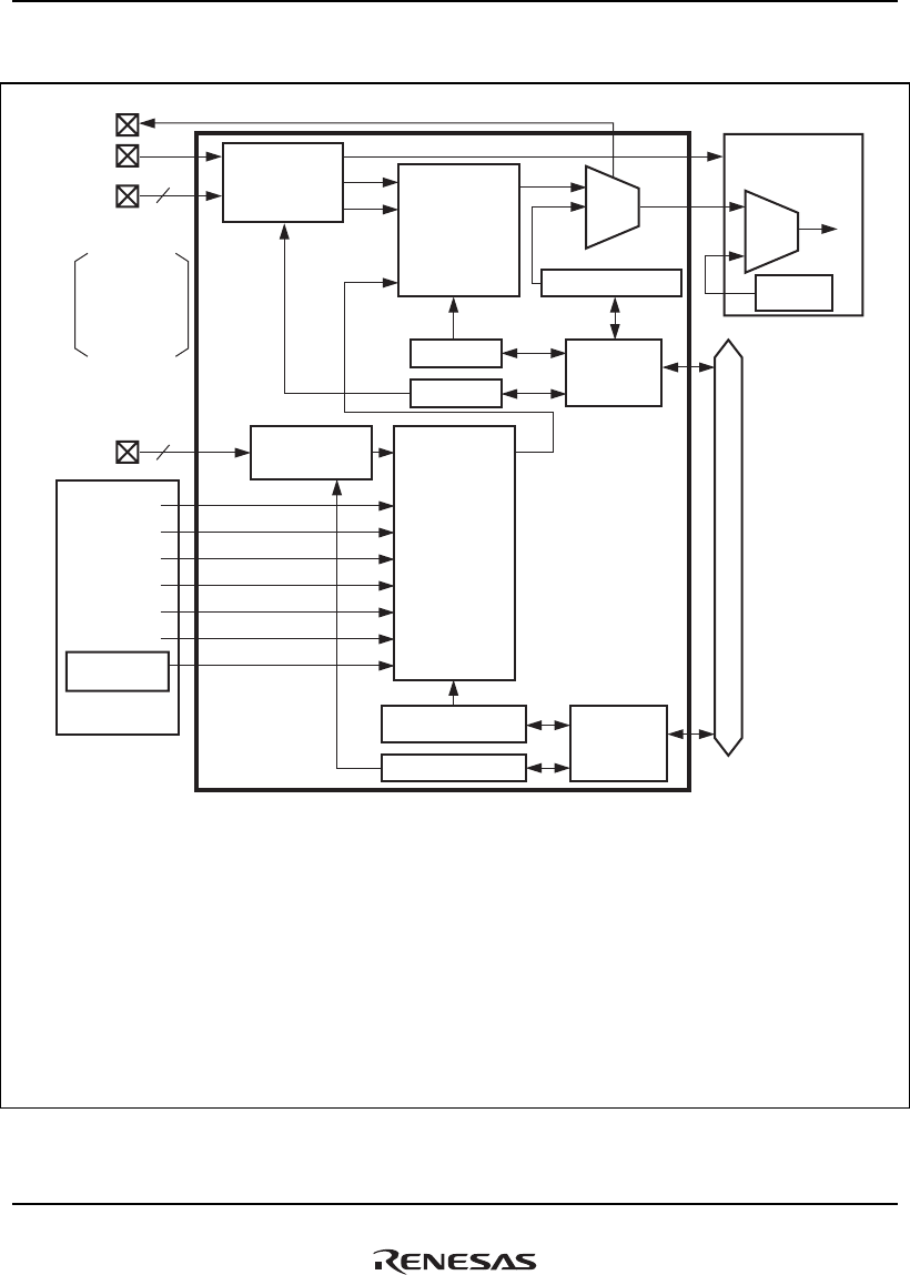
10. Interrupt Controller (INTC)
Rev.1.00 Jan. 10, 2008 Page 264 of 1658
REJ09B0261-0100
Figure 10.1 shows a block diagram of the INTC.
Input control Priority
determination
for external
interrupts
(levels 1 to 15)
Priority
determination
for on-chip
peripheral
module
interrupts
(levels 2 to 31)
Bus interface
WDT
H-UDI
DMAC
PCIC
DU
GDTA
GPIO interrupts
Interrupt request
USERIMASK.UIMASK
Comparator
Bus interface
Comparator
CPU
Interrupt
acceptance
INTPRI
SR.IMASK
ICR0, 1
INT2PRI0 to
INT2PRI9
INT2GPIC
Other peripheral
modules*
On-chip
modules
Interrupt request
Interrupt request
Interrupt request
Interrupt request
Interrupt request
Interrupt request
NMI
NMI
IRQOUT
IRQ/IRL7 to
IRQ/IRL4 and
GPIO port
L4 to L1 are
multiplexed
IRQ/IRL7 to
IRQ/IRL0
GPIO Port
E5 to E0
H4 to H1
L7, L6
IRL
IRQ
8
12
Peripheral bus
Note: * Other peripheral modules that can output interrupts are TMU, SCIF, HAC, SIOF, HSPI, MMCIF, SSI, and FLCTL.
Legend:
DMAC:
DU:
FLCTL:
GDTA:
HAC:
HSPI:
H-UDI:
ICR0, ICR1:
INTPRI:
INT2PRI0 to
INT2PRI9:
INT2GPIC:
Direct Memory Access Controller
Display Unit
NAND Flash Memory Controller
Graphics Data Translation Accelerator
Audio Codec Interface
Serial Peripheral Interface
User Debugging Interface
Interrupt Control Registers 0, 1
Interrupt Priority Level Register
Interrupt Priority Registers 0 to 9
GPIO Interrupt Set Register
MMCIF:
PCIC:
SCIF:
SIOF:
SR.IMASK:
SSI:
TMU:
USERIMASK.
UIMASK:
WDT:
Multimedia Card Interface
PCI Controller
Serial Communication Interface with FIFO
Synchronous Serial I/O with FIFO
IMASK bit in Status Register
Serial Sound Interface
Timer Unit
UIMASK bit in User Interrupt Mask Level Register
Watch Dog Timer
Figure 10.1 Block Diagram of INTC

10. Interrupt Controller (INTC)
Rev.1.00 Jan. 10, 2008 Page 265 of 1658
REJ09B0261-0100
The details of the input control circuit of figure 10.1 are shown in figure 10.2.
NMI
IRQ/IRL7 to
IRQ/IRL0
NMI
detector*4
Input control NMI interrupt
request
INTC
IRL
mask
controller
Noise
canceller
Noise
canceller
for level
detection
IRL
detector*2
Priority
determination
for external
interrupts
IRQ
detector*3
IRL/IRQ
pin mode
controller*1
ICR0
ICR1
INTMSK2
INTREQ
INTMSK1
INTMSK0
IRL
IRQ
Notes: 1. The internal signal for IRQ is fixed when ICR0.IRLMn (n = 0, 1) is cleared to 0, and the
internal signal for IRL is fixed when ICR0.IRLMn is set to 1 to prevent propagation of the state
transition on the pin to inside the LSI.
2. IRL detector includes a noise canceller.
When the interrupt source holding mode bit (ICR0.LVLMODE) is cleared to 0, the interrupt
source bits for the detected IRL interrupt request are retained in the INTC. When
ICR0.LVLMODE = 1, the interrupt source bits are not retained.
In the case of ICR0.LVLMODE = 0, if the IRL interrupt request masking is set by INTMSK2
after the interrupt source bit is retained, the IRL interrupt request of the source that has
already been retained will not be masked. To clear the retained interrupt request, refer to
section 10.7.1.
3. When the IRQ interrupt is configured for level-sense, the interrupt source bit of the IRQ
interrupt detected by this circuit is retained if ICR0.LVLMODE = 0. The interrupt source bits of
the level-sense IRQ are not retained if ICR0.LVLMODE = 1.
4. This circuit detects the NMI interrupt request.
Figure 10.2 Input Control Circuit for the Interrupt Requested from the External Pin

10. Interrupt Controller (INTC)
Rev.1.00 Jan. 10, 2008 Page 266 of 1658
REJ09B0261-0100
10.1.1 Interrupt Method
The basic flow of exception handling for interrupts is as follows.
In interrupt exception handling, the contents of the program counter (PC), status register (SR), and
general register 15 (R15) are saved in the saved program counter (SPC), saved status register
(SSR), and saved general register15 (SGR), and the CPU starts execution of the interrupt
exception handling routine at the corresponding vector address. An interrupt exception handling
routine is a program written by the user to handle a specific exception. The interrupt exception
handling routine is terminated and control returned to the original program by executing a return-
from-exception instruction (RTE). This instruction restores the contents of PC and SR and returns
control to the normal processing routine at the point at which the exception occurred. The contents
of SGR are not written back to R15 by the RTE instruction.
1. The contents of the PC, SR and R15 are saved in SPC, SSR and SGR, respectively.
2. The block (BL) bit in SR is set to 1.
3. The mode (MD) bit in SR is set to 1.
4. The register bank (RB) bit in SR is set to 1.
5. In a reset, the FPU disable (FD) bit in SR is cleared to 0.
6. The exception code is written to bits 13 to 0 of the interrupt event register (INTEVT).
7. Processing jumps to the start address of the interrupt exception handling routine, vector base
register (VBR) + H'600.
When the INTMU bit in CPOOPM is set to 1, the interrupt mask level (IMASK) in SR is
automatically modified to the level of the accepted interrupt.
8. The processing branches to the corresponding exception handling vector address and the
exception handling routine starts.

10. Interrupt Controller (INTC)
Rev.1.00 Jan. 10, 2008 Page 267 of 1658
REJ09B0261-0100
10.1.2 Interrupt Sources
Table 10.1 shows an example of the interrupt types. The INTC supports both external interrupts
and on-chip peripheral module interrupts.
External interrupts refer to the interrupts input through the external NMI, IRL, and IRQ pins.
The IRQ and IRL interrupts are assigned to the same pins in the SH7785. The pin functions are
selected to suit the system configuration.
Ether level-sense, or the rising or falling edge, can be selected for the detection of IRQ input.
Table 10.1 Interrupt Types
Source
Number of
Sources
(Max.) Priority INTEVT Remarks
NMI 1 16 H'1C0
H'200 IRL[3:0] = LLLL (H'0)
External
interrupts IRL 2
H'B00 IRL[7:4] = LLLL (H'0)
High
H'220 IRL[3:0] = LLLH (H'1)
H'B20 IRL[7:4] = LLLH (H'1)
H'240 IRL[3:0] = LLHL (H'2)
H'B40 IRL[7:4] = LLHL (H'2)
H'260 IRL[3:0] = LLHH (H'3)
H'B60 IRL[7:4] = LLHH (H'3)
H'280 IRL[3:0] = LHLL (H'4)
Inverse of values on the
input pins (because the
signals are active low)
Input level
H: high level
L: low level
(see table 10.11)
H'B80 IRL[7:4] = LHLL (H'4)
H'2A0 IRL[3:0] = LHLH (H'5)
H'BA0 IRL[7:4] = LHLH (H'5)
H'2C0 IRL[3:0] = LHHL (H'6)
H'BC0 IRL[7:4] = LHHL (H'6)
H'2E0 IRL[3:0] = LHHH (H'7)
H'BE0 IRL[7:4] = LHHH (H'7)
H'300 IRL[3:0] = HLLL (H'8)
H'C00 IRL[7:4] = HLLL (H'8) Low
10. Interrupt Controller (INTC)
Rev.1.00 Jan. 10, 2008 Page 268 of 1658
REJ09B0261-0100
Source
Number of
Sources
(Max.) Priority INTEVT Remarks
H'320 IRL[3:0] pin = HLLH (H'9)
H'C20 IRL[7:4] pin = HLLH (H'9)
H'340 IRL[3:0] pin = HLHL (H'A)
External
interrupts
IRL 2
H'C40 IRL[7:4] pin = HLHL (H'A)
High
H'360 IRL[3:0] pin = HLHH (H'B)
H'C60 IRL[7:4] pin = HLHH (H'B)
H'380 IRL[3:0] pin = HHLL (H'C)
H'C80 IRL[7:4] pin = HHLL (H'C)
H'3A0 IRL[3:0] pin = HHLH (H'D)
H'CA0 IRL[7:4] pin = HHLH (H'D)
H'3C0 IRL[3:0] pin = HHHL (H'E)
Inverse of values on
the input pins
(because the signals
are active low)
Input level
H: high level
L: low level
(see table 10.11)
H'CC0 IRL[7:4] pin = HHHL (H'E) Low
8 Values set in INTPRI H'240 IRQ[0] High
IRQ
interrupt H'280 IRQ[1]
H'2C0 IRQ[2]
H'300 IRQ[3]
H'340 IRQ[4]
H'380 IRQ[5]
H'3C0 IRQ[6]
H'200 IRQ[7] Low
WDT 1 H'560 ITI*
TMU-ch0 1
Values set in
INT2PRI0 to INT2PRI9 H'580 TUNI0*
TMU-ch1 1 H'5A0 TUNI1*
TMU-ch2 2 H'5C0 TUNI2*
On-chip
peripheral
module
interrupts*
H'5E0 TICPI2*
H-UDI 1 H'600 H-UDII
DMAC(0) 7 H'620 DMINT0*
H'640 DMINT1*
H'660 DMINT2*

10. Interrupt Controller (INTC)
Rev.1.00 Jan. 10, 2008 Page 269 of 1658
REJ09B0261-0100
Source
Number of
Sources
(Max.) Priority INTEVT Remarks
DMAC(0) 7 H'680 DMINT3*
H'6A0 DMINT4*
On-chip
module
interrupts*
Values set in INT2PRI0 to
INT2PRI9
H'6C0 DMINT5*
H'6E0 DMAE0 (channels 0 to 5)*
SCIF-ch0 4 H'700 ERI0*
H'720 RXI0*
H'740 BRI0*
H'760 TXI0*
SCIF-ch1 4 H'780 ERI1*
H'7A0 RXI1*
H'7C0 BRI1*
H'7E0 TXI1*
DMAC(1) 7 H'880 DMINT6*
H'8A0 DMINT7*
H'8C0 DMINT8*
H'8E0 DMINT9*
H'900 DMINT10*
H'920 DMINT11*
H'940 DMAE1 (channels 6 to 11)*
HSPI 1 H'960 SPII
SCIF-ch2 4 H'980 ERI2*, RXI2*, BRI2*, TXI2*
SCIF-ch3 4 H'9A0 ERI3*, RXI3*, BRI3*, TXI3*
SCIF-ch4 4 H'9C0 ERI4*, RXI4*, BRI4*, TXI4*
SCIF-ch5 4 H'9E0 ERI5*, RXI5*, BRI5*, TXI5*
PCIC(0) 4 H'A00 PCISERR
PCIC(1) 1 H'A20 PCIINTA
PCIC(2) 1 H'A40 PCIINTB
PCIC(3) 1 H'A60 PCIINTC
PCIC(4) 1 H'A80 PCIINTD
PCIC(5) 5 H'AA0 PCIERR
H'AC0 PCIPWD3, PCIPWD2,
PCIPWD1
H'AE0 PCIPWD0

10. Interrupt Controller (INTC)
Rev.1.00 Jan. 10, 2008 Page 270 of 1658
REJ09B0261-0100
Source
Number of
Sources
(Max.) Priority INTEVT Remarks
SIOF 1 H'CE0 SIOFI
MMCIF 4 H'D00 FSTAT
Values set in INT2PRI0 to
INT2PRI9
H'D20 TRAN
On-chip
module
interrupts*
H'D40 ERR
H'D60 FRDY
DU 1 H'D80 DUI
GDTA 3 H'DA0 GACLI
H'DC0 GAMCI
H'DE0 GAERI
TMU-ch3 1 H'E00 TUNI3*
TMU-ch4 1 H'E20 TUNI4*
TMU-ch5 1 H'E40 TUNI5*
SSI-ch0 1 H'E80 SSII0
SSI-ch1 1 H'EA0 SSII1
HAC-ch0 1 H'EC0 HACI0
HAC-ch1 1 H'EE0 HACI1
FLCTL 4 H'F00 FLSTE*
H'F20 FLTEND*
H'F40 FLTRQ0*
H'F60 FLTRQ1*
GPIO 4 H'F80 GPIOI0 (Port pins E0 to E2)
H'FA0 GPIOI1 (Port pins E3 to E5)
H'FC0 GPIOI2 (Port pins H1 to H4)
H'FE0 GPIOI3 (Port pins L6 and L7)
Legend:
ITI: WDT Interval timer interrupt
TUNI0 to TUNI5: TMU channels 0 to 5 underflow interrupt
TICPI2: TMU channel 2 input capture interrupt
DMINT0 to DMINT11: DMAC channels 0 to 11 transfer end interrupt
DMAE0 (ch0 to 5): DMAC address error interrupt (channels 0 to 5)
DMAE1 (ch6 to 11): DMAC address error interrupt (channels 6 to 11)
ERI0, ERI1, ERI2,
ERI3, ERI4, ERI5: SCIF channels 0 to 5 receive error interrupt
RXI0, RXI1, RXI2,
RXI3, RXI4, RXI5: SCIF channels 0 to 5 receive data full interrupt

10. Interrupt Controller (INTC)
Rev.1.00 Jan. 10, 2008 Page 271 of 1658
REJ09B0261-0100
BRI0, BRI1, BRI2,
BRI3, BRI4, BRI5: SCIF channels 0 to 5 break interrupt
TXI0, TXI1, TXI2, TXI3,
TXI4, TXI5: SCIF channels 0 to 5 transmission data empty interrupt
FLSTE: FLCTL error interrupt
FLTEND: FLCTL error interrupt
FLTRQ0: FLCTL data FIFO transfer request interrupt
FLTRQ1: FLCTL control code FIFO transfer request interrupt
Note: * Abbreviations used in the sources of the on-chip peripheral module interrupts.

10. Interrupt Controller (INTC)
Rev.1.00 Jan. 10, 2008 Page 272 of 1658
REJ09B0261-0100
10.2 Input/Output Pins
Table 10.2 shows the pin configuration.
Table 10.2 INTC Pin Configuration
Pin Name Function I/O Description
NMI Nonmaskable
interrupt
input pin
Input Nonmaskable interrupt request signal input
IRQ/IRL7 to
IRQ/IRL0
External
interrupt
input pins
Input Interrupt request signal input of IRQ7 to IRQ0 or IRL[7:4]
and IRL[3:0]
The IRQ/IRL7 pin is multiplexed with FD7 (FLCTL I/O),
MODE3 (mode control input), and port L1 (GPIO I/O) pin,
the IRQ/IRL6 pin is multiplexed with FD6 (FLCTL I/O),
MODE2 (mode control input), and port L2 (GPIO I/O) pin,
the IRQ/IRL5 pin is multiplexed with FD5 (FLCTL I/O),
MODE1 (mode control input), and port L3 (GPIO I/O) pin,
and the IRQ/IRL4 pin is multiplexed with FD4 (FLCTL I/O),
MODE3 (mode control input), and port L4 (GPIO I/O) pin.
IRQOUT Interrupt
request
output pin
Output Informs an external device of the generation of an interrupt
request.
The IRQOUT pin is multiplexed with MRESETOUT (reset,
watchdog timer (WDT) output pin).
IRQOUT outputs the low level even if the interrupt request is
not accepted by the CPU because of the priority of a
generated interrupt request being lower than SR.IMASK.
However, IRQOUT is not asserted in the following cases:
(1) IRL interrupt
• The IRL interrupt is masked by INTMASK1, or
• The IRQ interrupt is masked by INTMASK2.
(2) IRQ interrupt
• The interrupt is masked by INTMASK1, or
• The priority of the IRQ interrupt is set to H'0 by INTPRI
(3) On-chip module interrupt
• The on-chip module interrupt is masked by INT2MSKR,
or
• The priority is set to H'00 or H'01 by INT2PRI0 to
INT2PRI9.

10. Interrupt Controller (INTC)
Rev.1.00 Jan. 10, 2008 Page 273 of 1658
REJ09B0261-0100
10.3 Register Descriptions
Table 10.3 shows the INTC register configuration. Table 10.4 shows the register states in each
operating mode.
Table 10.3 INTC Register Configuration
Name Abbreviation R/W P4 Address Area 7 Address
Access
Size
Sync.
Clock
Interrupt control register 0 ICR0 R/W H'FFD0 0000 H'1FD0 0000 32 Pck
Interrupt control register 1 ICR1 R/W H'FFD0 001C H'1FD0 001C 32 Pck
Interrupt priority register INTPRI R/W H'FFD0 0010 H'1FD0 0010 32 Pck
Interrupt source register INTREQ R/(W)*1H'FFD0 0024 H'1FD0 0024 32 Pck
Interrupt mask register 0 INTMSK0 R/W H'FFD0 0044 H'1FD0 0044 32 Pck
Interrupt mask register 1 INTMSK1 R/W H'FFD0 0048 H'1FD0 0048 32 Pck
Interrupt mask register 2 INTMSK2 R/W H'FFD4 0080 H'1FD4 0080 32 Pck
Interrupt mask clear register 0 INTMSKCLR0 R/W H'FFD0 0064 H'1FD0 0064 32 Pck
Interrupt mask clear register 1 INTMSKCLR1 R/W H'FFD0 0068 H'1FD0 0068 32 Pck
Interrupt mask clear register 2 INTMSKCLR2 R/W H'FFD4 0084 H'1FD4 0084 32 Pck
NMI flag control register NMIFCR R/(W)*2H'FFD0 00C0 H'1FD0 00C0 32 Pck
User interrupt mask level
register
USERIMASK R/W H'FFD3 0000 H'1FD3 0000 32 Pck
INT2PRI0 R/W H'FFD4 0000 H'1FD4 0000 32 Pck
INT2PRI1 R/W H'FFD4 0004 H'1FD4 0004 32 Pck
Interrupt priority registers
INT2PRI2 R/W H'FFD4 0008 H'1FD4 0008 32 Pck
INT2PRI3 R/W H'FFD4 000C H'1FD4 000C 32 Pck
INT2PRI4 R/W H'FFD4 0010 H'1FD4 0010 32 Pck
INT2PRI5 R/W H'FFD4 0014 H'1FD4 0014 32 Pck
INT2PRI6 R/W H'FFD4 0018 H'1FD4 0018 32 Pck
INT2PRI7 R/W H'FFD4 001C H'1FD4 001C 32 Pck
INT2PRI8 R/W H'FFD4 0020 H'1FD4 0020 32 Pck
INT2PRI9 R/W H'FFD4 0024 H'1FD4 0024 32 Pck
Interrupt source register (not
affected by the mask state)
INT2A0 R H'FFD4 0030 H'1FD4 0030 32 Pck

10. Interrupt Controller (INTC)
Rev.1.00 Jan. 10, 2008 Page 274 of 1658
REJ09B0261-0100
Name Abbreviation R/W P4 Address Area 7 Address
Access
Size
Sync.
Clock
Interrupt source register
(affected by the mask state)
INT2A1 R H'FFD4 0034 H'1FD4 0034 32 Pck
Interrupt mask register INT2MSKR R/W H'FFD4 0038 H'1FD4 0038 32 Pck
Interrupt mask clear register INT2MSKCLR R/W H'FFD4 003C H'1FD4 003C 32 Pck
INT2B0 R H'FFD4 0040 H'1FD4 0040 32 Pck
INT2B1 R H'FFD4 0044 H'1FD4 0044 32 Pck
On-chip module interrupt
source registers
INT2B2 R H'FFD4 0048 H'1FD4 0048 32 Pck
INT2B3 R H'FFD4 004C H'1FD4 004C 32 Pck
INT2B4 R H'FFD4 0050 H'1FD4 0050 32 Pck
INT2B5 R H'FFD4 0054 H'1FD4 0054 32 Pck
INT2B6 R H'FFD4 0058 H'1FD4 0058 32 Pck
INT2B7 R H'FFD4 005C H'1FD4 005C 32 Pck
GPIO interrupt set register INT2GPIC R/W H'FFD4 0090 H'1FD4 0090 32 Pck
Notes: 1. The interrupt source registers (INTREQ) are readable and conditionally writable
registers. For details, refer to section 10.3.1, External Interrupt Request Registers.
2. The NMI flag control register (NMIFCR) is readable and conditionally writable register.
For details, refer to section 10.3.1, External Interrupt Request Registers.

10. Interrupt Controller (INTC)
Rev.1.00 Jan. 10, 2008 Page 275 of 1658
REJ09B0261-0100
Table 10.4 Register States in Each Operating Mode
Name Abbreviation
Power-on
Reset by
PRESET
Pin/WDT/H-UDI
Manual Reset
by
WDT/Multiple
Exception
Sleep by
SLEEP
Instruction
Deep Sleep by
SLEEP
Instruction
(DSLP = 1)
Interrupt control
register 0
ICR0 H'x000 0000* H'x000 0000* Retained Retained
Interrupt control
register 1
ICR1 H'0000 0000 H'0000 0000 Retained Retained
Interrupt priority
register
INTPRI H'0000 0000 H'0000 0000 Retained Retained
Interrupt source
register
INTREQ H'0000 0000 H'0000 0000 Retained Retained
Interrupt mask
register 0
INTMSK0 H'0000 0000 H'0000 0000 Retained Retained
Interrupt mask
register 1
INTMSK1 H'FF00 0000 H'FF00 0000 Retained Retained
Interrupt mask
register 2
INTMSK2 H'FF00 0000 H'FF00 0000 Retained Retained
Interrupt mask clear
register 0
INTMSKCLR0 H'xx00 0000 H'xx00 0000 Retained Retained
Interrupt mask clear
register 1
INTMSKCLR1 H'x000 0000 H'x000 0000 Retained Retained
Interrupt mask clear
register 2
INTMSKCLR2 H'xxxx xxxx H'xxxx xxxx Retained Retained
NMI flag control
register
NMIFCR H'x000 0000* H'x000 0000* Retained Retained
User interrupt mask
level register
USERIMASK H'0000 0000 H'0000 0000 Retained Retained
INT2PRI0 H'0000 0000 H'0000 0000 Retained Retained
INT2PRI1 H'0000 0000 H'0000 0000 Retained Retained
Interrupt priority
registers
INT2PRI2 H'0000 0000 H'0000 0000 Retained Retained
INT2PRI3 H'0000 0000 H'0000 0000 Retained Retained
INT2PRI4 H'0000 0000 H'0000 0000 Retained Retained
INT2PRI5 H'0000 0000 H'0000 0000 Retained Retained
INT2PRI6 H'0000 0000 H'0000 0000 Retained Retained

10. Interrupt Controller (INTC)
Rev.1.00 Jan. 10, 2008 Page 276 of 1658
REJ09B0261-0100
Name Abbreviation
Power-on
Reset by
PRESET
Pin/WDT/H-UDI
Manual Reset
by
WDT/Multiple
Exception
Sleep by
SLEEP
Instruction
Deep Sleep by
SLEEP
Instruction
(DSLP = 1)
INT2PRI7 H'0000 0000 H'0000 0000 Retained Retained
INT2PRI8 H'0000 0000 H'0000 0000 Retained Retained
Interrupt priority
registers
INT2PRI9 H'0000 0000 H'0000 0000 Retained Retained
Interrupt source
register (not affected
by the mask state)
INT2A0 H'xxxx xxxx H'xxxx xxxx Retained Retained
Interrupt source
register (affected by
the mask state)
INT2A1 H'0000 0000 H'0000 0000 Retained Retained
Interrupt mask
register
INT2MSKR H'FFFF FFFF H'FFFF FFFF Retained Retained
Interrupt mask clear
register
INT2MSKCR H'0000 0000 H'0000 0000 Retained Retained
INT2B0 H'xxxx xxxx H'xxxx xxxx Retained Retained
INT2B1 H'xxxx xxxx H'xxxx xxxx Retained Retained
Module interrupt
source registers
INT2B2 H'xxxx xxxx H'xxxx xxxx Retained Retained
INT2B3 H'xxxx xxxx H'xxxx xxxx Retained Retained
INT2B4 H'xxxx xxxx H'xxxx xxxx Retained Retained
INT2B5 H'xxxx xxxx H'xxxx xxxx Retained Retained
INT2B6 H'xxxx xxxx H'xxxx xxxx Retained Retained
INT2B7 H'xxxx xxxx H'xxxx xxxx Retained Retained
GPIO interrupt set
register
INT2GPIC H'0000 0000 H'0000 0000 Retained Retained
Note: * initial values of ICR0.NMIL and NMIFCR.NMIL depend on the level input to the NMI pin.

10. Interrupt Controller (INTC)
Rev.1.00 Jan. 10, 2008 Page 277 of 1658
REJ09B0261-0100
10.3.1 External Interrupt Request Registers
(1) Interrupt Control Register 0 (ICR0)
ICR0 is a 32-bit readable and partially writable register that sets the input signal detection mode
for the external interrupt input pins and NMI pin, and indicates the level being input on the NMI
pin.
161718192021222324252627282931 30
00000000000000—0
⎯⎯⎯⎯⎯
LVL
MODE
IRLM1IRLM0
NMIENMIB
⎯⎯⎯⎯
NMIL MAI
RRRRRR/WR/WR/WR/WR/WRRRRR R/W
Bit:
Initial value:
R/W:
01234567891011121315 14
0000000000000000
⎯⎯⎯⎯⎯⎯⎯⎯⎯⎯⎯⎯⎯⎯⎯⎯
RRRRRRRRRRRRRRRR
Bit:
Initial value:
R/W:
Bit Name
Initial
Value R/W Description
31 NMIL Undefined R NMI Input Level
Indicates the signal level being input on the NMI pin.
Reading this bit allows the user to know the NMI pin
level, and writing is invalid.
0: Low level is being input on the NMI pin
1: High level is being input on the NMI pin
30 MAI 0 R/W MAI (mask all interrupts) Interrupt Mask
Specifies whether all interrupts are masked while the
NMI pin is at the low level regardless of the setting of
the BL bit in SR of the CPU.
0: Interrupts remain enabled even when the NMI pin
goes low
1: Interrupts are disabled when the NMI pin goes low
29 to 26 ⎯ All 0 R Reserved
These bits are always read as 0. The write value
should always be 0.

10. Interrupt Controller (INTC)
Rev.1.00 Jan. 10, 2008 Page 278 of 1658
REJ09B0261-0100
Bit Name
Initial
Value R/W Description
25 NMIB 0 R/W NMI Block Mode
Selects whether an NMI interrupt is held until the BL bit
in SR is cleared to 0 or detected immediately when the
BL bit in SR of the CPU is set to 1.
0: An NMI interrupt is held when the BL bit in SR is set
to 1 (initial value)
1: An NMI interrupt is not held when the BL bit in SR is
set to 1
Note: If interrupts are accepted with the BL bit in SR
set to 1, information saved for any previous
exception (SSR, SPC, SGR, and INTEVT) is lost.
24 NMIE 0 R/W NMI Edge Select
Selects whether an interrupt request signal to the NMI
pin is detected at the rising edge or the falling edge.
0: An interrupt request is detected at the falling edge of
NMI input (initial value)
1: An interrupt request is detected at the rising edge of
NMI input
23 IRLM0*1*2 0 R/W IRL Pin Mode 0
Selects whether IRQ/IRL3 to IRQ/IRL0 are used as
encoded interrupt requests (IRL3 to IRL0) or as four
independent interrupts (IRQ3 to IRQ0 interrupts).
0: IRQ/IRL3 to IRQ/IRL0 are used as the encoded
interrupt requests (initial value)
1: IRQ/IRL3 to IRQ/IRL0 are used as four independent
interrupt requests
22 IRLM1*1*2 0 R/W IRL Pin Mode 1
Selects whether IRQ/IRL7 to IRQ/IRL4 are used as 4-
bit level-encoded interrupt requests (IRL7 to IRL4
interrupts) or as four independent interrupts (IRQ7 to
IRQ4 interrupts).
0: IRQ/IRL7 to IRQ/IRL4 are used as the 4-bit level-
encoded interrupt requests (initial value)
1: IRQ/IRL7 to IRQ/IRL4 are used as four independent
interrupt requests

10. Interrupt Controller (INTC)
Rev.1.00 Jan. 10, 2008 Page 279 of 1658
REJ09B0261-0100
Bit Name
Initial
Value R/W Description
21 LVLMODE 0 R/W Level-sense IRQ/IRL with holding function
Selects whether or not to use the holding function for
level-sense IRQ and IRL interrupts.
0: Level-sense IRQ and IRL interrupt requests are held
(initial value)
1: Level-sense IRQ and IRL interrupt requests are not
held
Rewriting to this bit should be performed by the
initialization routine before canceling the masking
(INTMASK0 and INTMASK1) for the IRQ interrupts and
IRL interrupt. After this, do not rewrite this bit until
power-on reset or manual reset is made. The initial
value is 0, however. it is recommended to use INTC
after this bit has been set to 1 by the initialization
routine.
For the details of the operation when this bit is set to 0,
refer to section 10.4.2, IRQ Interrupts, section 10.4.3,
IRL Interrupts, section 10.7.1, Example of Handing
Routine of IRL Interrupts and Level Detection IRQ
Interrupts when ICR0.LVLMODE = 0, and section
10.7.3, Clearing IRQ and IRL Interrupt Requests.
20 to 0 ⎯ All 0 R Reserved
These bits are always read as 0. The write value
should always be 0.
Notes: 1. When IRLM0 and IRLM1 are changed from 0 to 1, the IRL interrupt source that has
been detected or held is cleared. When IRLM0 and IRLM1 are changed from 1 to 0, the
IRL interrupt source that has been detected or held is not cleared.
2. When using the IRQ/IRL3 to IRQ/IRL0 pins or IRQ/IRL7 to IRQ/IRL4 pins as encoded
IRL interrupt inputs, set IM00 to IM03 or IM04 to IM07 of the interrupt mask register 0 to
1, respectively.
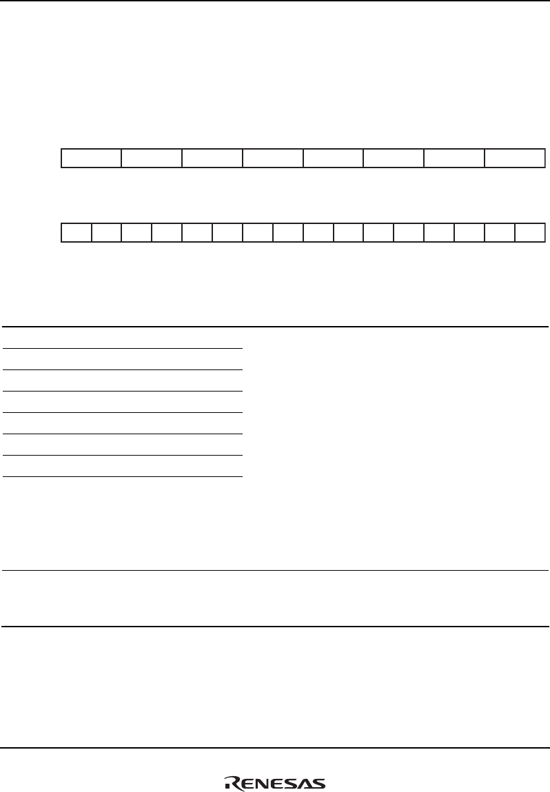
10. Interrupt Controller (INTC)
Rev.1.00 Jan. 10, 2008 Page 280 of 1658
REJ09B0261-0100
(2) Interrupt Control Register 1 (ICR1)
ICR1 is a 32-bit readable/writable register that specifies the individual input signal detection
modes for the respective external interrupt input pins IRQ/IRL7 to IRQ/IRL0. These settings are
only valid when IRLM0 or IRLM1 of ICR0 is set to 1 so that IRQ/IRL3 to IRQ/IRL0 or
IRQ/IRL7 to IRQ/IRL4 pins are used as individual interrupts (IRQ7 to IRQ0 interrupts) inputs.
161718192021222324252627282931 30
0000000000000000
IRQ7SIRQ6SIRQ5SIRQ4SIRQ3SIRQ2SIRQ0S IRQ1S
R/WR/WR/WR/WR/WR/WR/WR/WR/WR/WR/WR/WR/WR/WR/W R/W
Bit:
Initial value:
R/W:
01234567891011121315 14
0000000000000000
⎯⎯⎯⎯⎯⎯⎯⎯⎯⎯⎯⎯⎯⎯⎯⎯
RRRRRRRRRRRRRRRR
Bit:
Initial value:
R/W:
Bit Name
Initial
Value R/W Description
31, 30 IRQ0S 00 R/W
29, 28 IRQ1S 00 R/W
27, 26 IRQ2S 00 R/W
25, 24 IRQ3S 00 R/W
23, 22 IRQ4S 00 R/W
21, 20 IRQ5S 00 R/W
19, 18 IRQ6S 00 R/W
17, 16 IRQ7S 00 R/W
IRQn Sense Select
Selects whether the corresponding individual pin
interrupt signal on the IRQ/IRL7 to IRQ/IRL0 pins is
detected on rising or falling edges, or at the high or
low level.
00: The interrupt request is detected on falling edges
of the IRQn input.
01: The interrupt request is detected on rising edges
of the IRQn input.
10: The interrupt request is detected when the IRQn
input is at the low level.
11: The interrupt request is detected when the IRQn
input is at the high level.
Note: n = 0 to 7
15 to 0 ⎯ All 0 R Reserved
These bits are always read as 0. The write value
should always be 0.
Notes: 1. When an IRQ pin is set for level input (IRQnS1 = 1) and the source holding mode
(LVLMODE of ICR0) of the interrupt control register 0 (ICR0) is 0, the interrupt source is
held until the CPU accepts the interrupt (this is also true for other interrupts). Therefore,
even if an interrupt source is disabled before this LSI returns from sleep mode,
branching of processing to the interrupt handler when this LSI returns from sleep mode
is guaranteed. A held interrupt can be cleared by setting the corresponding interrupt
mask bit (the IM bit in the interrupt mask register) to 1 (refer to section 10.7.3, Clearing

10. Interrupt Controller (INTC)
Rev.1.00 Jan. 10, 2008 Page 281 of 1658
REJ09B0261-0100
IRQ and IRL Interrupt Requests).
2. When the IRQnS setting is changed from edge sense (IRQnS is 00 or 01) to level
sense (IRQnS is 10 or 11), the IRQ interrupt source that has been edge sensed is
cleared. When the IRQnS setting is changed from level sense (IRQnS is 10 or 11) to
edge sense (IRQnS is 00 or 01), the IRQ interrupt source that has been sensed or held
is cleared. When the IRQnS setting is changed form falling-edge sense (IRQnS is 00) to
rising edge sense (IRQnS is 01), or changed from rising edge sense (IRQnS is 01) to
the falling edge sense (IRQnSis 00), the IRQ interrupt source that has been sensed
before changing the setting is not cleared. Likewise, when IRQnS setting is changed
from low-level sense (IRQnS is 10) to high-level sense (IRQnS is 11), or changed from
high-level sense (IRQnS is 11) to the low-level sense (IRQnSis 10), the IRQ interrupt
source that has been sensed before changing the setting is not cleared.
10. Interrupt Controller (INTC)
Rev.1.00 Jan. 10, 2008 Page 282 of 1658
REJ09B0261-0100
(3) Interrupt Priority Register (INTPRI)
INTPRI is a 32-bit readable/writable register used to set the priorities of IRQ[7:0] (as levels from
15 to 0). These settings are only valid for IRQ/IRL7 to IRQ/IRL4 or IRQ/IRL3 to IRQ/IRL0 when
set up as individual IRQ interrupts (IRQ7 to IRQ0 interrupts) by setting the IRLM0 or IRLM1 bit
in ICR0 to 1.
161718192021222324252627282931 30
0000000000000000
IP3IP2IP1IP0
R/WR/WR/WR/WR/WR/WR/WR/WR/WR/WR/WR/WR/WR/WR/W R/W
R/WR/WR/WR/WR/WR/WR/WR/WR/WR/WR/WR/WR/WR/WR/W R/W
Bit:
Initial value:
R/W:
01234567891011121315 14
0000000000000000
IP7IP6IP5IP4
Bit:
Initial value:
R/W:
Bit Name
Initial
Value R/W Description
31 to 28 IP0 H'0 R/W Set the priority of IRQ0 as an individual pin interrupt request.
27 to 24 IP1 H'0 R/W Set the priority of IRQ1 as an individual pin interrupt request.
23 to 20 IP2 H'0 R/W Set the priority of IRQ2 as an individual pin interrupt request.
19 to 16 IP3 H'0 R/W Set the priority of IRQ3 as an individual pin interrupt request.
15 to 12 IP4 H'0 R/W Set the priority of IRQ4 as an individual pin interrupt request.
11 to 8 IP5 H'0 R/W Set the priority of IRQ5 as an individual pin interrupt request.
7 to 4 IP6 H'0 R/W Set the priority of IRQ6 as an individual pin interrupt request.
3 to 0 IP7 H'0 R/W Set the priority of IRQ7 as an individual pin interrupt request.
Note: Interrupt priorities are established by setting values from H'F to H'1 in each of the 4-bit
fields. A larger value corresponds to a higher priority. When the value H'0 is set in a field,
the corresponding interrupt request is masked (initial value).
10. Interrupt Controller (INTC)
Rev.1.00 Jan. 10, 2008 Page 283 of 1658
REJ09B0261-0100
(4) Interrupt Source Register (INTREQ)
INTREQ is a 32-bit readable and conditionally writable register that indicates which of the IRQ
[n] (n = 0 to 7) interrupts is currently asserting a request for the INTC.
Even if an interrupt is masked by the setting in INTPRI or INTMSK0, operation of the
corresponding INTREQ bit is not affected.
161718192021222324252627282931 30
0000000000000000
⎯⎯⎯⎯⎯⎯
⎯⎯IR7IR6
IR5IR4IR3IR2
IR0 IR1
RRRRRRRRR/(W)R/(W)R/(W)R/(W)R/(W)R/(W)R/(W) R/(W)
Bit:
Initial value:
R/W:
01234567891011121315 14
0000000000000000
⎯⎯⎯⎯⎯⎯⎯⎯⎯⎯⎯⎯⎯⎯⎯⎯
RRRRRRRRRRRRRRRR
Bit:
Initial value:
R/W:
Description
Bit Name
Initial
Value R/W
Edge Detection
(IRQnS = 00 or 01)*1
Level Detection
(IRQnS = 10 or 11)*1
31 IR0 0 R/(W)
30 IR1 0 R/(W)
29 IR2 0 R/(W)
28 IR3 0 R/(W)
27 IR4 0 R/(W)
26 IR5 0 R/(W)
25 IR6 0 R/(W)
24 IR7 0 R/(W)
[When read]
0: The corresponding IRQ
interrupt request has not
been detected.
1: The corresponding IRQ
interrupt request has been
detected.
[When written]*2
When clearing each bit, write a
0 after having read a 1 from it.
Writing 1 to the bit is ignored.
[When read]
(ICR0.LVLMODE = 0)
0: The corresponding interrupt
source has not been
detected.
1: The corresponding interrupt
source has been detected.
[When read]
(ICR0.LVLMODE = 1)
0: The corresponding IRQ
interrupt pin is not asserted.
1: The corresponding IRQ
interrupt pin is asserted, but
the CPU has not accepted
the interrupt request yet.
Writing have no effect.*3
23 to 0 ⎯ All 0 R Reserved
These bits are always read as 0. The write value should always
be 0.
Notes: 1. n = 0 to 7
2. Write 1 to the bit if it should not be cleared yet.
3. For the method of clearing the IRQ interrupt request that has been detected by level
sensing, refer to section 10.7.3, Clearing IRQ and IRL Interrupt Requests.

10. Interrupt Controller (INTC)
Rev.1.00 Jan. 10, 2008 Page 284 of 1658
REJ09B0261-0100
(5) Interrupt Mask Register 0 (INTMSK0)
INTMSK0 is a 32-bit readable and conditionally writable register that sets masking for each of the
interrupt requests IRQn (n = 0 to 7). To clear the mask setting for an interrupt, write 1 to the
corresponding bit in INTMSKCLR0. Writing 0 to the bits in INTMSK0 has no effect. By reading
this register once after writing to this register or after clearing the mask by setting
IMTMSKCLR0, the time length necessary for reflecting the register value can be assured (the
value read is reflected to the mask status).
When using IRQ/IRL3 to IRQ/IRL0 pins or IRQ/IRL7 to IRQ/IRL4 pins for encoded IRL
interrupt inputs, write 1 to IM00 to IM03 or IM04 to IM07, respectively.
161718192021222324252627282931 30
0000000011111111
⎯⎯⎯⎯⎯⎯
⎯⎯IM07IM06
IM05IM04IM03IM02
IM00 IM01
RRRRRRRRR/WR/WR/WR/WR/WR/WR/W R/W
Bit:
Initial value:
R/W:
01234567891011121315 14
0000000000000000
⎯⎯⎯⎯⎯⎯⎯⎯⎯⎯⎯⎯⎯⎯⎯⎯
RRRRRRRRRRRRRRRR
Bit:
Initial value:
R/W:
Bit Name
Initial
Value R/W Description
31 IM00 1 R/W Sets masking of individual
pin interrupt source on
IRQ0.
30 IM01 1 R/W Sets masking of individual
pin interrupt source on
IRQ1.
29 IM02 1 R/W Sets masking of individual
pin interrupt source on
IRQ2.
28 IM03 1 R/W Sets masking of individual
pin interrupt source on
IRQ3.
[When read]
0: The interrupts are
accepted.
1: The interrupts are
masked.
[When written]
0: No effect
1: Masks the interrupt
27 IM04 1 R/W Sets masking of individual
pin interrupt source on
IRQ4.

10. Interrupt Controller (INTC)
Rev.1.00 Jan. 10, 2008 Page 285 of 1658
REJ09B0261-0100
Bit Name
Initial
Value R/W Description
26 IM05 1 R/W Sets masking of individual
pin interrupt source on
IRQ5.
25 IM06 1 R/W Sets masking of individual
pin interrupt source on
IRQ6.
24 IM07 1 R/W Sets masking of individual
pin interrupt source on
IRQ7.
[When read]
0: The interrupts are
accepted.
1: The interrupts are
masked.
[When written]
0: No effect
1: Masks the interrupt
23 to 0 All 0 R Reserved
These bits are always read as 0. The write value
should always be 0.

10. Interrupt Controller (INTC)
Rev.1.00 Jan. 10, 2008 Page 286 of 1658
REJ09B0261-0100
(6) Interrupt Mask Register 1 (INTMSK1)
INTMSK1 is a 32-bit readable and conditionally writable register that sets masking for IRL
interrupt requests. To clear the mask setting for the interrupt, write 1 to the corresponding bit in
INTMSKCLR1. Writing 0 to the bits in INTMSK1 has no effect. By reading this register once
after writing to this register or after clearing the mask by setting IMTMSKCLR1, the time length
necessary for reflecting the register value can be assured (the value read is reflected to the mask
status).
161718192021222324252627282931 30
0000000011111111
⎯⎯⎯⎯⎯⎯
⎯⎯⎯⎯
⎯⎯⎯⎯
IM10 IM11
RRRRRRRRRRRRRRR/W R/W
Bit:
Initial value:
R/W:
01234567891011121315 14
0000000000000000
⎯⎯⎯⎯⎯⎯⎯⎯⎯⎯⎯⎯⎯⎯⎯⎯
RRRRRRRRRRRRRRRR
Bit:
Initial value:
R/W:
Bit Name
Initial
Value R/W Description
31 IM10 1 R/W Mask setting for all IRL3 to
IRL0 interrupt sources
when pins IRQ/IRL3 to
IRQ/IRL0 operate as an
encoded interrupt input.
30 IM11 1 R/W Mask setting for all IRL7 to
IRL4 interrupt sources
when pins IRQ/IRL7 to
IRQ/IRL4 operate as an
encoded interrupt input.
[When read]
0: The interrupt is
accepted.
1: The interrupt is
masked.
[When written]
0: No effect
1: Masks the interrupt
29 to 24 ⎯ All 1 R Reserved
These bits are always read as 1. The write value
should always be 1.
23 to 0 ⎯ All 0 R Reserved
These bits are always read as 0. The write value
should always be 0.

10. Interrupt Controller (INTC)
Rev.1.00 Jan. 10, 2008 Page 287 of 1658
REJ09B0261-0100
(7) Interrupt Mask Register 2 (INTMSK2)
INTMSK2 is a 32-bit readable and conditionally writable register that sets masking for IRL
interrupt requests for input level pattern on the IRL pins. To clear the mask setting for the
interrupt, write 1 to the corresponding bit in INTMSKCLR2. Writing 0 to the bits in INTMSK2
has no effect. By reading this register once after writing to this register or after clearing the mask
by setting IMTMSKCLR2, the time length necessary for reflecting the register value can be
assured (the value read is reflected to the mask status).
INTMSK2 settings are valid when the IRQ/IRL3 to IRQ/IRL0 pins or IRQ/IRL7 to IRQ/IRL4
pins are used for encoded IRL interrupt inputs, and the corresponding IRL interrupt is not masked
by INTMSK1.
161718192021222324252627282931 30
0000000000000000
⎯IM001IM002IM003IM004IM005
IM006IM007IM008IM009
IM010IM011IM012IM013
IM015 IM014
RR/WR/WR/WR/WR/WR/WR/WR/WR/WR/WR/WR/WR/WR/W R/W
RR/WR/WR/WR/WR/WR/WR/WR/WR/WR/WR/WR/WR/WR/W R/W
Bit:
Initial value:
R/W:
01234567891011121315 14
0000000000000000
⎯IM101IM102IM103IM104IM105IM106IM107IM108IM109IM110IM111IM112IM113IM115 IM114
Bit:
Initial value:
R/W:
Bit Name
Initial
Value R/W Description
31 IM015 0 R/W Masks the interrupt source
of IRL3 to IRL0 = LLLL
(H'0).
30 IM014 0 R/W Masks the interrupt source
of IRL3 to IRL0 = LLLH
(H'1).
29 IM013 0 R/W Masks the interrupt source
of IRL3 to IRL0 = LLHL
(H'2).
[When read]
0: The interrupt is
accepted.
1: The interrupt is
masked.
[When written]
0: No effect
1: Masks the interrupt
28 IM012 0 R/W Masks the interrupt source
of IRL3 to IRL0 = LLHH
(H'3).
27 IM011 0 R/W Masks the interrupt source
of IRL3 to IRL0 = LHLL
(H'4).

10. Interrupt Controller (INTC)
Rev.1.00 Jan. 10, 2008 Page 288 of 1658
REJ09B0261-0100
Bit Name
Initial
Value R/W Description
26 IM010 0 R/W Masks the interrupt source
of IRL3 to IRL0 = LHLH
(H'5).
25 IM009 0 R/W Masks the interrupt source
of IRL3 to IRL0 = LHHL
(H'6).
24 IM008 0 R/W Masks the interrupt source
of IRL3 to IRL0 = LHHH
(H'7).
23 IM007 0 R/W Masks the interrupt source
of IRL3 to IRL0 = HLLL
(H'8).
22 IM006 0 R/W Masks the interrupt source
of IRL3 to IRL0 = HLLH
(H'9).
21 IM005 0 R/W Masks the interrupt source
of IRL3 to IRL0 = HLHL
(H'A).
[When read]
0: The interrupt is
accepted.
1: The interrupt is
masked.
[When written]
0: No effect
1: Masks the interrupt
20 IM004 0 R/W Masks the interrupt source
of IRL3 to IRL0 = HLHH
(H'B).
19 IM003 0 R/W Masks the interrupt source
of IRL3 to IRL0 = HHLL
(H'C).
18 IM002 0 R/W Masks the interrupt source
of IRL3 to IRL0 = HHLH
(H'D).
17 IM001 0 R/W Masks the interrupt source
of IRL3 to IRL0 = HHHL
(H'E).
16 — 0 R Reserved
This bit is always read as 0. The write value should
always be 0.

10. Interrupt Controller (INTC)
Rev.1.00 Jan. 10, 2008 Page 289 of 1658
REJ09B0261-0100
Bit Name
Initial
Value R/W Description
15 IM115 0 R/W Masks the interrupt source
of IRL7 to IRL4 = LLLL
(H'0).
14 IM114 0 R/W Masks the interrupt source
of IRL7 to IRL4 = LLLH
(H'1).
13 IM113 0 R/W Masks the interrupt source
of IRL7 to IRL4 = LLHL
(H'2).
12 IM112 0 R/W Masks the interrupt source
of IRL7 to IRL4 = LLHH
(H'3).
[When read]
0: The interrupt is
accepted.
1: The interrupt is
masked.
[When written]
0: No effect
1: Masks the interrupt
11 IM111 0 R/W Masks the interrupt source
of IRL7 to IRL4 = LHLL
(H'4).
10 IM110 0 R/W Masks the interrupt source
of IRL7 to IRL4 = LHLH
(H'5).
9 IM109 0 R/W Masks the interrupt source
of IRL7 to IRL4 = LHHL
(H'6).
8 IM108 0 R/W Masks the interrupt source
of IRL7 to IRL4 = LHHH
(H'7).
7 IM107 0 R/W Masks the interrupt source
of IRL7 to IRL4 = HLLL
(H'8).
6 IM106 0 R/W Masks the interrupt source
of IRL7 to IRL4 = HLLH
(H'9).
5 IM105 0 R/W Masks the interrupt source
of IRL7 to IRL4 = HLHL
(H'A).
4 IM104 0 R/W Masks the interrupt source
of IRL7 to IRL4 = HLHH
(H'B).
3 IM103 0 R/W Masks the interrupt source
of IRL7 to IRL4 = HHLL
(H'C).

10. Interrupt Controller (INTC)
Rev.1.00 Jan. 10, 2008 Page 290 of 1658
REJ09B0261-0100
Bit Name
Initial
Value R/W Description
2 IM102 0 R/W Masks the interrupt source
of IRL7 to IRL4 = HHLH
(H'D).
1 IM101 0 R/W Masks the interrupt source
of IRL7 to IRL4 = HHHL
(H'E).
[When read]
0: The interrupt is
accepted.
1: The interrupt is
masked.
[When written]
0: No effect
1: Masks the interrupt
0 — 0 R Reserved
This bit is always read as 0. The write value should
always be 0.

10. Interrupt Controller (INTC)
Rev.1.00 Jan. 10, 2008 Page 291 of 1658
REJ09B0261-0100
(8) Interrupt Mask Clear Register 0 (INTMSKCLR0)
INTMSKCLR0 is a 32-bit write-only register that clears the mask settings for each of the interrupt
requests IRQn (n = 0 to 7). Undefined values are read from this register.
161718192021222324252627282931 30
0000000000000000
⎯⎯⎯⎯⎯⎯
⎯⎯IC07IC06
IC05IC04IC03IC02
IC00 IC01
RRRRRRRRR/WR/WR/WR/WR/WR/WR/W R/W
Bit:
Initial value:
R/W:
01234567891011121315 14
0000000000000000
⎯⎯⎯⎯⎯⎯⎯⎯⎯⎯⎯⎯⎯⎯⎯⎯
RRRRRRRRRRRRRRRR
Bit:
Initial value:
R/W:
Bit Name
Initial
Value R/W Description
31 IC00 0 R/W Clears masking of IRQ0
interrupt.
30 IC01 0 R/W Clears masking of IRQ1
interrupt.
29 IC02 0 R/W Clears masking of IRQ2
interrupt.
28 IC03 0 R/W Clears masking of IRQ3
interrupt.
27 IC04 0 R/W Clears masking of IRQ4
interrupt.
26 IC05 0 R/W Clears masking of IRQ5
interrupt.
25 IC06 0 R/W Clears masking of IRQ6
interrupt.
24 IC07 0 R/W Clears masking of IRQ7
interrupt.
[When read]
Undefined values are
read.
[When written]
0: No effect
1: Clears the
corresponding interrupt
mask (enables the
interrupt)
23 to 0 — All 0 R Reserved
These bits are always read as 0. The write value
should always be 0.

10. Interrupt Controller (INTC)
Rev.1.00 Jan. 10, 2008 Page 292 of 1658
REJ09B0261-0100
(9) Interrupt Mask Clear Register 1 (INTMSKCLR1)
INTMSKCLR1 is a 32-bit write-only register that clears the mask settings for the IRL interrupt
requests. Undefined values are read from this register.
161718192021222324252627282931 30
0000000000000000
⎯⎯⎯⎯⎯⎯
⎯⎯⎯⎯
⎯⎯⎯⎯
IC10 IC11
RRRRRRRRRRRRRRR/W R/W
Bit:
Initial value:
R/W:
01234567891011121315 14
0000000000000000
⎯⎯⎯⎯⎯⎯⎯⎯⎯⎯⎯⎯⎯⎯⎯⎯
RRRRRRRRRRRRRRRR
Bit:
Initial value:
R/W:
Bit Name
Initial
Value R/W Description
31 IC10 0 R/W Clears masking of IRL3 to
IRL0 interrupt sources
when IRL3 to IRL0 operate
as an encoded interrupt
input.
30 IC11 0 R/W Clears masking of IRL7 to
IRL4 interrupt sources
when IRL7 to IRL4 operate
as an encoded interrupt
input.
[When read]
Undefined values are read.
[When written]
0: No effect
1: Clears the
corresponding interrupt
mask (enables the
interrupt)
29 to 0 ⎯ All 0 R Reserved
These bits are always read as 0. The write value should
always be 0.

10. Interrupt Controller (INTC)
Rev.1.00 Jan. 10, 2008 Page 293 of 1658
REJ09B0261-0100
(10) Interrupt Mask Clear Register 2 (INTMSKCLR2)
INTMSKCLR2 is a 32-bit write-only register that clears the mask settings for the IRL interrupt
requests for each input level pattern on the IRL pins. Undefined values are read from this register.
161718192021222324252627282931 30
0000000000000000
⎯IC001IC002IC003IC004IC005
IC006IC007IC008IC009
IC010IC011IC012IC013
IC015 IC014
RR/WR/WR/WR/WR/WR/WR/WR/WR/WR/WR/WR/WR/WR/W R/W
Bit:
Initial value:
R/W:
01234567891011121315 14
0000000000000000
⎯IC101IC102IC103IC104IC105IC106IC107IC108IC109IC110IC111IC112IC113IC115 IC114
RR/WR/WR/WR/WR/WR/WR/WR/WR/WR/WR/WR/WR/WR/W R/W
Bit:
Initial value:
R/W:
Bit Name
Initial
Value R/W Description
31 IC015 0 R/W Clears masking of the
interrupt source of IRL3 to
IRL0 = LLLL (H'0).
30 IC014 0 R/W Clears masking of the
interrupt source of IRL3 to
IRL0 = LLLH (H'1).
29 IC013 0 R/W Clears masking of the
interrupt source of IRL3 to
IRL0 = LLHL (H'2).
28 IC012 0 R/W Clears masking of the
interrupt source of IRL3 to
IRL0 = LLHH (H'3).
[When read]
Undefined values are
read.
[When written]
0: No effect
1: Clears the
corresponding interrupt
mask (enables the
interrupt)
27 IC011 0 R/W Clears masking of the
interrupt source of IRL3 to
IRL0 = LHLL (H'4).
26 IC010 0 R/W Clears masking of the
interrupt source of IRL3 to
IRL0 = LHLH (H'5).
25 IC009 0 R/W Clears masking of the
interrupt source of IRL3 to
IRL0 = LHHL (H'6).
24 IC008 0 R/W Clears masking of the
interrupt source of IRL3 to
IRL0 = LHHH (H'7).

10. Interrupt Controller (INTC)
Rev.1.00 Jan. 10, 2008 Page 294 of 1658
REJ09B0261-0100
Bit Name
Initial
Value R/W Description
23 IC007 0 R/W Clears masking of the
interrupt source of IRL3 to
IRL0 = HLLL (H'8).
22 IC006 0 R/W Clears masking of the
interrupt source of IRL3 to
IRL0 = HLLH (H'9).
21 IC005 0 R/W Clears masking of the
interrupt source of IRL3 to
IRL0 = HLHL (H'A).
20 IC004 0 R/W Clears masking of the
interrupt source of IRL3 to
IRL0 = HLHH (H'B).
19 IC003 0 R/W Clears masking of the
interrupt source of IRL3 to
IRL0 = HHLL (H'C).
[When read]
Undefined values are
read.
[When written]
0: No effect
1: Clears the
corresponding interrupt
mask (enables the
interrupt)
18 IC002 0 R/W Clears masking of the
interrupt source of IRL3 to
IRL0 = HHLH (H'D).
17 IC001 0 R/W Clears masking of the
interrupt source of IRL3 to
IRL0 = HHHL (H'E).
16 — 0 R Reserved
This bit is always read as 0. The write value should
always be 0.
15 IC115 0 R/W Clears masking of the
interrupt source of IRL7 to
IRL4 = LLLL (H'0).
14 IC114 0 R/W Clears masking of the
interrupt source of IRL7 to
IRL4 = LLLH (H'1).
13 IC113 0 R/W Clears masking of the
interrupt source of IRL7 to
IRL4 = LLHL (H'2).
12 IC112 0 R/W Clears masking of the
interrupt source of IRL7 to
IRL4 = LLHH (H'3).
[When read]
Undefined values are
read.
[When written]
0: No effect
1: Clears the
corresponding interrupt
mask (enables the
interrupt)

10. Interrupt Controller (INTC)
Rev.1.00 Jan. 10, 2008 Page 295 of 1658
REJ09B0261-0100
Bit Name
Initial
Value R/W Description
11 IC111 0 R/W Clears masking of the
interrupt source of IRL7 to
IRL4 = LHLL (H'4).
10 IC110 0 R/W Clears masking of the
interrupt source of IRL7 to
IRL4 = LHLH (H'5).
9 IC109 0 R/W Clears masking of the
interrupt source of IRL7 to
IRL4 = LHHL (H'6).
8 IC108 0 R/W Clears masking of the
interrupt source of IRL7 to
IRL4 = LHHH (H'7).
7 IC107 0 R/W Clears masking of the
interrupt source of IRL7 to
IRL4 = HLLL (H'8).
[When read]
Undefined values are
read.
[When written]
0: No effect
1: Clears the
corresponding interrupt
mask (enables the
Interrupt)
6 IC106 0 R/W Clears masking of the
interrupt source of IRL7 to
IRL4 = HLLH (H'9).
5 IC105 0 R/W Clears masking of the
interrupt source of IRL7 to
IRL4 = HLHL (H'A).
4 IC104 0 R/W Clears masking of the
interrupt source of IRL7 to
IRL4 = HLHH (H'B).
3 IC103 0 R/W Clears masking of the
interrupt source of IRL7 to
IRL4 = HHLL (H'C).
2 IC102 0 R/W Clears masking of the
interrupt source of IRL7 to
IRL4 = HHLH (H'D).
1 IC101 0 R/W Clears masking of the
interrupt source of IRL7 to
IRL4 = HHHL (H'E).
0 — 0 R Reserved
This bit is always read as 0. The write value should
always be 0.

10. Interrupt Controller (INTC)
Rev.1.00 Jan. 10, 2008 Page 296 of 1658
REJ09B0261-0100
(11) NMI Flag Control Register (NMIFCR)
NMIFCR is a 32-bit readable and conditionally writable register that has an NMI flag (NMIFL
bit). The NMIFL bit is automatically set to 1 when an NMI interrupt is detected by the INTC.
Writing 0 to the NMIFL bit clears it.
The value of the NMIFL bit does not affect acceptance of the NMI by the CPU. Although an NMI
request detected by the INTC is cleared when the CPU accepts the NMI, the NMIFL bit is not
cleared automatically. Even if 0 is written to the NMIFL bit before the NMI request is accepted by
the CPU, the NMI request is not canceled.
161718192021222324252627282931 30
00000000000000x0
NMIFL
⎯⎯⎯⎯⎯⎯⎯⎯⎯⎯⎯⎯⎯NMIL ⎯
R/(W)RRRRRRRRRRRRRRR
Bit:
Initial value:
R/W:
01234567891011121315 14
0000000000000000
⎯⎯⎯⎯⎯⎯⎯⎯⎯⎯⎯⎯⎯⎯⎯⎯
RRRRRRRRRRRRRRRR
Bit:
Initial value:
R/W:
Bit Name
Initial
Value R/W Description
31 NMIL x R NMI Input Level
Indicates the level of the signal input to the NMI pin;
that is, this bit is read to determine the level on the NMI
pin. This bit cannot be modified.
0: The low level is being input to the NMI pin
1: The high level is being input to the NMI pin
30 to 17 — All 0 R Reserved
These bits are always read as 0. The write value
should always be 0.

10. Interrupt Controller (INTC)
Rev.1.00 Jan. 10, 2008 Page 297 of 1658
REJ09B0261-0100
Bit Name
Initial
Value R/W Description
16 NMIFL 0 R/(W) NMI Flag (NMI Interrupt Request Detection)
Indicates whether an NMI interrupt request signal has
been detected. This bit is automatically set to 1 when
the INTC detects an NMI interrupt request. Write 0 to
clear the bit. Writing 1 to this bit has no effect.
[When read]
1: NMI has been detected
0: NMI has not been detected
[When written]
0: Clears the NMI flag
1: No effect
15 to 0 — All 0 R Reserved
These bits are always read as 0. The write value
should always be 0.
10. Interrupt Controller (INTC)
Rev.1.00 Jan. 10, 2008 Page 298 of 1658
REJ09B0261-0100
10.3.2 User Mode Interrupt Disable Function
(1) User Interrupt Mask Level Setting Register (USERIMASK)
USERIMASK is a 32-bit readable and conditionally writable register that sets the acceptable
interrupt level. This register is allocated to the 64-Kbyte page that the other registers in the INTC
are not allocated. Therefore, only this register can be set to be accessible in user mode by changing
the address to area 7 address through the MMU.
The interrupts that the level is lower than the level set in the UIMASK bits are masked. When H'F
is set in the UIMASK bit, all interrupts other than the NMI are masked.
The interrupts that the level is higher than the level set in the UIMASK bits are accepted under the
following conditions. The corresponding interrupt mask bit in the interrupt mask register is cleared
to 0 (the interrupt is enabled). The IMASK bit in SR is set lower than its interrupt level.
The value of the UIMASK bit does not change even if an interrupt is accepted.
USERIMASK is initialized to H'0000 0000 (all interrupts are enabled) by a power-on reset or
manual reset.
To prevent incorrect writing, this register should not be written to unless bits 31 to 24 are set to
H'A5.
161718192021222324252627282931 30
0000000000000000
⎯⎯⎯⎯⎯⎯⎯⎯
RRRRRRRRR/WR/WR/WR/WR/WR/WR/W R/W
Bit:
Initial value:
R/W:
01234567891011121315 14
0000000000000000
⎯⎯⎯⎯UIMASK⎯⎯⎯⎯⎯⎯⎯⎯
RRRRR/WR/WR/WR/WRRRRRRRR
Bit:
Initial value:
R/W:
Code for writing (H'A5)

10. Interrupt Controller (INTC)
Rev.1.00 Jan. 10, 2008 Page 299 of 1658
REJ09B0261-0100
Bit Name
Initial
Value R/W Description
31 to 24 (Code for
writing)
H'00 R/W Code for writing (H'A5)
These bits are always read as 0. Set these bits to H'A5
when writing to the UIMASK bits (Write to the UIMASK
bits with these bits set to H'A5).
23 to 8 — All 0 R Reserved
These bits are always read as 0. The write value
should always be 0.
7 to 4 UIMASK 0 R/W Interrupt Mask Level
The interrupts whose level is equal to or lower than the
value set in the UIMASK bits are masked.
3 to 0 — All 0 R Reserved
These bits are always read as 0. The write value
should always be 0.
(2) Procedure for Using the User Interrupt Mask Level Register
By setting the interrupt mask level in USERIMASK, the interrupts whose level is equal to or
lower than the value set in USERIMASK are disabled. This function is used to disable less urgent
interrupts when more urgent processing is performed by the tasks such as device drivers operating
in user mode to reduce the processing time.
USERIMASK is allocated in a different 64-Kbyte space apart from the one where other INTC
registers are allocated. Access to this register in user mode involves address translation by the
MMU. In a multitasking OS, the memory-protection functions of the MMU should be used to
control the processes that can access USERIMASK. Clear USERIMASK to 0 before completing a
task or switching to another task. If a task is completed with the UIMASK bits set to a value other
than 0, the interrupts whose level is equal to or lower than UIMASK remain disabled. This can
lead to problems, for example, the OS may not be able to switch between tasks.
An example procedure for using USERIMASK is described below.
1. Classify interrupts into A and B, as described below. Then, set the interrupt level of A-type
interrupts higher than that of the B-priority interrupts.
A. Interrupts to be accepted by device drivers (interrupts used in the OS, such as a timer
interrupt)
B. Interrupts that should not be accepted by device drivers
2. Set the MMU so that the access to the address space containing USERIMASK is only allowed
for the device drivers that need to disable the interrupts.
10. Interrupt Controller (INTC)
Rev.1.00 Jan. 10, 2008 Page 300 of 1658
REJ09B0261-0100
3. Branch to the device driver.
4. In the device driver operating in user mode, set the UIMASK bits to mask the B-type
interrupts.
5. Process more urgent interrupts in the device driver.
6. Clear the UIMASK bit to 0 and return from the processing by the device driver.
10.3.3 On-chip Module Interrupt Priority Registers
(1) Interrupt Priority Registers (INT2PRI0 to INT2PRI9)
INT2PRI0 to INT2PRI9 are 32-bit readable/writable registers that set priority levels (31 to 0) of
the on-chip peripheral module interrupts. These registers are initialized to H'0000 0000 by a reset.
These registers can set the priority of each interrupt source in 30 levels (H'00 and H'01 mask the
interrupt request) by the 5-bit field.
161718192021222324252627282931 30
0000000000000000
⎯⎯⎯⎯⎯⎯
R/WR/WR/WR/WR/WRRRR/WR/WR/WR/WR/WRRR
Bit:
Initial value:
R/W:
01234567891011121315 14
0000000000000000
⎯⎯⎯⎯⎯⎯
R/WR/WR/WR/WR/WRRRR/WR/WR/WR/WR/WRRR
Bit:
Initial value:
R/W:
Table 10.5 shows the correspondence between interrupt request sources and bits in INT2PRI0 to
INT2PRI9.

10. Interrupt Controller (INTC)
Rev.1.00 Jan. 10, 2008 Page 301 of 1658
REJ09B0261-0100
Table 10.5 Interrupt Request Sources and INT2PRI0 to INT2PRI9
Bits
Register 28 to 24 20 to 16 12 to 8 4 to 0
INT2PRI0 TMU channel 0 TMU channel 1 TMU channel 2 TMU channel 2
input capture
INT2PRI1 TMU channel 3 TMU channel 4 TMU channel 5 Reserved*
INT2PRI2 SCIF channel 0 SCIF channel 1 SCIF channel 2 SCIF channel 3
INT2PRI3 SCIF channel 4 SCIF channel 5 WDT Reserved*
INT2PRI4 H-UDI DMAC (0) DMAC (1) Reserved*
INT2PRI5 HAC channel 0 HAC channel 1 PCIC (0) PCIC (1)
INT2PRI6 PCIC (2) PCIC (3) PCIC (4) PCIC (5)
INT2PRI7 SIOF HSPI MMCIF Reserved*
INT2PRI8 FLCTL GPIO SSI channel 0 SSI channel 1
INT2PRI9 DU GDTA Reserved* Reserved*
Notes: The larger the value is, the higher the priority is. If the value is set to H'00 or H'01, the
request is masked. For details, see table 10.1, Interrupt Sources.
* Reserved bits are always read as 0. The write value should always be 0.

10. Interrupt Controller (INTC)
Rev.1.00 Jan. 10, 2008 Page 302 of 1658
REJ09B0261-0100
(2) Interrupt Source Register (Not affected by Mask Setting) (INT2A0)
INT2A0 is a 32-bit read-only register that indicates the interrupt sources of on-chip peripheral
modules. Even if an interrupt is masked by the interrupt mask register, the corresponding bit in
INT2A0 is set (further interrupt operation is not performed for the corresponding bit). Use
INT2A1 instead if the bits for the interrupt sources masked by the interrupt mask registers should
not be set.
161718192021222324252627282931 30
—————————————000
———
RRRRRRRRRRRRRRRR
Bit:
Initial value:
R/W:
01234567891011121315 14
————————————————
RRRRRRRRRRRRRRRR
Bit:
Initial value:
R/W:
Table 10.6 shows the correspondence between bits in INT2A0 and the interrupt sources.
Table 10.6 Correspondence between Bits in INT2A0 and Interrupt Sources
Bit
Initial
Value R/W Source Function Description
31 to
29
All 0 R Reserved These bits are always read
as 0. The write value
should always be 0.
28 Undefined R GDTA GDTA interrupt source
indication
27 Undefined R DU DU interrupt source
indication
26 Undefined R SSI
channel 1
SSI channel 1 interrupt
source indication
25 Undefined R SSI
channel 0
SSI channel 0 interrupt
source indication
24 Undefined R GPIO GPIO interrupt source
indication
23 Undefined R FLCTL FLCTL interrupt source
indication
These bits indicate the
interrupt source of each
peripheral module that is
generating an interrupt.
(INT2A0 is not affected by the
setting of the interrupt mask
register).
0: No interrupt
1: An interrupt has occurred
Note: Interrupt sources can
also be identified by
directly reading the
INTEVT code. In this
case, reading from this
register is not required.
22 Undefined R MMCIF MMCIF interrupt source
indication

10. Interrupt Controller (INTC)
Rev.1.00 Jan. 10, 2008 Page 303 of 1658
REJ09B0261-0100
Bit
Initial
Value R/W Source Function Description
21 Undefined R HSPI HSPI interrupt source
indication
20 Undefined R SIOF SIOF interrupt source
indication
19 Undefined R PCIC (5) PCIERR and PCIPWD3 to
PCIPWD0 interrupt source
indication
18 Undefined R PCIC (4) PCIINTD interrupt source
indication
17 Undefined R PCIC (3) PCIINTC interrupt source
indication
16 Undefined R PCIC (2) PCIINTB interrupt source
indication
15 Undefined R PCIC (1) PCIINTA interrupt source
indication
These bits indicate the
interrupt source of each
peripheral module that is
generating an interrupt.
(INT2A0 is not affected by the
setting of the interrupt mask
register).
0: No interrupt
1: An interrupt has occurred
Note: Interrupt sources can
also be identified by
directly reading the
INTEVT code. In this
case, reading from this
register is not required.
14 Undefined R PCIC (0) PCISERR interrupt source
indication
13 Undefined R HAC
channel 1
HAC channel 1 interrupt
source indication
12 Undefined R HAC
channel 0
HAC channel 0 interrupt
source indication
11 Undefined R DMAC (1) DMAC channels 6 to 11
and address error interrupt
source indication
10 Undefined R DMAC (0) DMAC channels 0 to 5 and
address error interrupt
source indication
9 Undefined R H-UDI H-UDI interrupt source
indication
8 Undefined R WDT WDT interrupt source
indication
7 Undefined R SCIF
channel 5
SCIF channel 5 interrupt
source indication
6 Undefined R SCIF
channel 4
SCIF channel 4 interrupt
source indication

10. Interrupt Controller (INTC)
Rev.1.00 Jan. 10, 2008 Page 304 of 1658
REJ09B0261-0100
Bit
Initial
Value R/W Source Function Description
5 Undefined R SCIF
channel 3
SCIF channel 3 interrupt
source indication
4 Undefined R SCIF
channel 2
SCIF channel 2 interrupt
source indication
3 Undefined R SCIF
channel 1
SCIF channel 1 interrupt
source indication
2 Undefined R SCIF
channel 0
SCIF channel 0 interrupt
source indication
1 Undefined R TMU
channels 3
to 5
TMU channel 3 to 5
interrupt source indication
0 Undefined R TMU
channels 0
to 2
TMU channel 0 to 2
interrupt source indication
These bits indicate the
interrupt source of each
peripheral module that is
generating an interrupt.
(INT2A0 is not affected by the
setting of the interrupt mask
register).
0: No interrupt
1: An interrupt has occurred
Note: Interrupt sources can
also be identified by
directly reading the
INTEVT code. In this
case, reading from this
register is not required.
If the interrupt source in an individual module is set or cleared, the time required until the state is
reflected in INT2A0 is as shown in table 10.7.

10. Interrupt Controller (INTC)
Rev.1.00 Jan. 10, 2008 Page 305 of 1658
REJ09B0261-0100
Table 10.7 Reflection time for INT2A0 and INT2A1 when Interrupt Source Bit in
Peripheral Module Is Set/Cleared
Module
Relation between Setting/Clearing Interrupt Source of
Module and Indication by INT2A0 and INT2A1
WDT, TMU, SCIF, HSPI, SIOF,
MMCIF, DU, SSI, HAC, FLCTL
When an interrupt source bit is set in the register* in the
module that indicates generation of interrupt requests, the
same interrupt status information is read from that register and
INT2A0 or INT2A1. This means that the time required for
reflection in INT2A0 and INT2A1 is guaranteed by hardware.
When an interrupt source is cleared, the status after the source
is cleared can be read from INT2A0 or INT2A1 if read after
clearing the interrupt source flag in the module.
H-UDI, GDTA When an interrupt source bit is set in the register* in the
module that indicates generation of interrupt requests (SDINT
in the H-UDI, GACISR in the GDTA), the same interrupt status
information is read from that register and INT2A0 or INT2A1.
This means that the time required for reflection in INT2A0 and
INT2A1 is guaranteed by hardware.
When an interrupt source is cleared, the time required for
reflection in INT2A0 and INT2A1 can be guaranteed by
dummy-reading SDINT in the H-UDI or GACISR in the GDTA
once after clearing the interrupt source flag in the module.
PCIC (excluding the pin input-
related interrupt sources
PCIINTA, PCIINTB, PCIINTC,
and PCIINTD)
When a PCIC interrupt source bit is set in PCIIR, PCIAINT, or
PCIPINT that indicates generation of interrupt requests, the
time required for reflection in INT2A0 and INT2A1 is
guaranteed by dummy-reading an arbitrary register in the INTC
once and then reading from INT2A0 or INT2A1.
When a PCIC interrupt source is cleared, the time required for
reflection in INT2A0 and INT2A1 is guaranteed in this way:
after writing to PCIIR, PCIAINT, or PCIPINT, dummy-read
PCIIR, PCIAINT, or PCIPINT once and then dummy-read an
arbitrary register in the INTC.

10. Interrupt Controller (INTC)
Rev.1.00 Jan. 10, 2008 Page 306 of 1658
REJ09B0261-0100
Module
Relation between Setting/Clearing Interrupt Source of
Module and Indication by INT2A0 and INT2A1
DMAC Interrupt sources
DMAE0, DMAE1
When the DMAE0 or DMAE1 interrupt source bit (i.e. the AE bit
in DMAOR0 or DMAOR1) is set, the same interrupt status
information is read from registers DMAOR0 and DMAOR1 and
registers INT2A0 and INT2A1. This means that the time
required for reflection in INT2A0 and INT2A1 is guaranteed by
hardware.
When the DMAE0 or DMAE1 interrupt source is cleared, the
time required for reflection in INT2A0 and INT2A1 is
guaranteed by dummy reading DMAOR0 or DMAOR1 once
after writing to DMAOR0 or DMAOR1.
Interrupt sources
DMINT0 to
DMINT11
Setting of the HE and TE bits in CHCR0 to CHCR11 and output
of interrupt request to the INTC take place with different timing.
For details, see section 14, Direct Memory Access Controller
(DMAC).
When interrupt sources, DMINT0 to DMINT11 (corresponding
to bits HE and TE in CHCR0 to CHCR11) are cleared, the time
required for reflection in INT2A0 and INT2A1 is guaranteed by
dummy-reading CHCR0 to CHCR11 once after writing to
CHCR0 to CHCR11 that indicate generation of interrupt
requests.
Note: The registers in the modules that indicate generation of interrupt requests are as follows.
WDT: WDTCSR
TMU: TCR0 to TCR5
SCIF: SCFSR0 to SCFSR6, SCLSR0 to SCLSR6
HSPI: SPSR
SIOF: SISTR
MMCIF: INTSTR0 to INTSTR2
DU: DSSR
SSI: SSISR
HAC: HACTSR, HACRSR
FLCTL: FLINTDMACR, FLTRCR

10. Interrupt Controller (INTC)
Rev.1.00 Jan. 10, 2008 Page 307 of 1658
REJ09B0261-0100
(3) Interrupt Source Register (Affected by Mask States) (INT2A1)
INT2A1 is a 32-bit read-only register that indicates the interrupt sources of on-chip peripheral
modules. If an interrupt is masked by the interrupt mask register, the corresponding bit in INT2A1
is not set to 1. Use INT2A0 to check whether interrupts have been generated, regardless of the
state of the interrupt mask register.
161718192021222324252627282931 30
0000000000000000
⎯⎯⎯
RRRRRRRRRRRRRRRR
Bit:
Initial value:
R/W:
01234567891011121315 14
0000000000000000
RRRRRRRRRRRRRRRR
Bit:
Initial value:
R/W:
Table 10.8 shows the correspondence between bits in INT2A1 and the interrupt sources.
Table 10.8 Correspondence between Bits in INT2A1 and Interrupt Sources
Bit
Initial
Value R/W Source Function Description
31 to
29
0 R Reserved These bits are read as 0
and cannot be modified.
28 0 R GDTA GDTA interrupt source
indication
27 0 R DU DU interrupt source
indication
26 0 R SSI channel 1 SSI channel 1 interrupt
source indication
25 0 R SSI channel 0 SSI channel 0 interrupt
source indication
24 0 R GPIO GPIO interrupt source
indication
These bits indicate the interrupt
source of each peripheral module
that is generating an interrupt.
(INT2A1 is affected by the setting
of the interrupt mask register).
0: No interrupt
1: An interrupt has occurred
Note: Interrupt sources can also
be identified by directly
reading the INTEVT code.
In this case, reading from
this register is not required.
23 0 R FLCTL FLCTL interrupt source
indication
22 0 R MMCIF MMCIF interrupt source
indication
21 0 R HSPI HSPI interrupt source
indication

10. Interrupt Controller (INTC)
Rev.1.00 Jan. 10, 2008 Page 308 of 1658
REJ09B0261-0100
Bit
Initial
Value R/W Source Function Description
20 0 R SIOF SIOF interrupt source
indication
19 0 R PCIC (5) PCIERR and PCIPWD3 to
PCIPWD0 interrupt source
indication
18 0 R PCIC (4) PCIINTD interrupt source
indication
17 0 R PCIC (3) PCIINTC interrupt source
indication
16 0 R PCIC (2) PCIINTB interrupt source
indication
15 0 R PCIC (1) PCIINTA interrupt source
indication
14 0 R PCIC (0) PCISERR interrupt source
indication
13 0 R HAC channel
1
HAC channel 1 interrupt
source indication
12 0 R HAC channel
0
HAC channel 0 interrupt
source indication
11 0 R DMAC (1) DMAC channels 6 to 11 and
address error interrupt
source indication
10 0 R DMAC (0) DMAC channels 0 to 5 and
address error interrupt
source indication
9 0 R
H-UDI H-UDI interrupt source
indication
These bits indicate the interrupt
source of each peripheral module
that is generating an interrupt.
(INT2A1 is affected by the setting
of the interrupt mask register).
0: No interrupt
1: An interrupt has occurred
Note: Interrupt sources can also
be identified by directly
reading the INTEVT code.
In this case, reading from
this register is not required.
8 0 R
WDT WDT interrupt source
indication
7 0 R
SCIF
channel 5
SCIF channel 5 interrupt
source indication
6 0 R
SCIF
channel 4
SCIF channel 4 interrupt
source indication
5 0 R
SCIF
channel 3
SCIF channel 3 interrupt
source indication
4 0 R
SCIF
channel 2
SCIF channel 2 interrupt
source indication

10. Interrupt Controller (INTC)
Rev.1.00 Jan. 10, 2008 Page 309 of 1658
REJ09B0261-0100
Bit
Initial
Value R/W Source Function Description
3 0 R
SCIF
channel 1
SCIF channel 1 interrupt
source indication
2 0 R
SCIF
channel 0
SCIF channel 0 interrupt
source indication
1 0 R
TMU
channels
3 to 5
TMU channel 3 to 5 interrupt
source indication
0 0 R
TMU
channels
0 to 2
TMU channel 0 to 2 interrupt
source indication
These bits indicate the interrupt
source of each peripheral module
that is generating an interrupt.
(INT2A1 is affected by the setting
of the interrupt mask register).
0: No interrupt
1: An interrupt has occurred
Note: Interrupt sources can also
be identified by directly
reading the INTEVT code.
In this case, reading from
this register is not required.
If the interrupt source in an individual module is set or cleared, the time required until the state is
reflected in INT2A1 is as shown in table 10.7.
If the interrupt masking is set by INT2MSKR or the interrupt masking by INT2MSKR is cleared
by INT2MSKCLR, the reflection time required for INT2A1 is guaranteed by hardware. Therefore,
after the interrupt mask is set or cleared, the contents that reflect the setting of INT2MSKR can be
read.

10. Interrupt Controller (INTC)
Rev.1.00 Jan. 10, 2008 Page 310 of 1658
REJ09B0261-0100
(4) Interrupt Mask Register (INT2MSKR)
INT2MSKR is a 32-bit readable/writable register that can mask interrupts for sources indicated in
the interrupt source register. When a bit in this register is set to 1, the interrupt in the
corresponding bit is not notified. INT2MSKR is initialized to H'FFFF FFFF (all masked) by a
reset.
After this register is written to or the masking is cleared by writing to INT2MSKCLR, the timing
required to reflect the register value is guaranteed by reading from this register once.
161718192021222324252627282931 30
1111111111111111
⎯⎯⎯
R/WR/WR/WR/WR/WR/WR/WR/WR/WR/WR/WR/WR/WRRR
Bit:
Initial value:
R/W:
01234567891011121315 14
1111111111111111
R/WR/WR/WR/WR/WR/WR/WR/WR/WR/WR/WR/WR/WR/WR/W R/W
Bit:
Initial value:
R/W:
Table 10.9 shows the correspondence between bits in INT2MSKR and the interrupts that are
masked.
Table 10.9 Correspondence between Bits in INT2MSKR and Interrupts that Are Masked
Bit
Initial
Value R/W Source Function Description
31 to
29
All 1 R Reserved These bits are always read as 1.
The write value should always be 1.
28 1 R/W GDTA Masks GDTA interrupt
27 1 R/W DU Masks DU interrupt
26 1 R/W SSI channel 1 Masks the SSI channel 1 interrupt
25 1 R/W SSI channel 0 Masks the SSI channel 0 interrupt
24 1 R/W GPIO Masks the GPIO interrupt
23 1 R/W FLCTL Masks the FLCTL interrupt
22 1 R/W MMCIF Masks the MMCIF interrupt
21 1 R/W HSPI Masks the HSPI interrupt
Masks interrupt of each
on-chip peripheral
module
[When written]
0: Invalid
1: Interrupt is masked
[When read]
0: Not masked
1: Masked
20 1 R/W SIOF Masks the SIOF interrupt
19 1 R/W PCIC (5) Masks PCIERR and PCIPWD3 to
PCIPWD0 interrupt

10. Interrupt Controller (INTC)
Rev.1.00 Jan. 10, 2008 Page 311 of 1658
REJ09B0261-0100
Bit
Initial
Value R/W Source Function Description
18 1 R/W PCIC (4) Masks the PCIINTD interrupt
17 1 R/W PCIC (3) Masks the PCIINTC interrupt
16 1 R/W PCIC (2) Masks the PCIINTB interrupt
15 1 R/W PCIC (1) Masks the PCIINTA interrupt
14 1 R/W PCIC (0) Masks the PCISERR interrupt
13 1 R/W HAC channel 1 Masks the HAC channel 1 interrupt
12 1 R/W HAC channel 0 Masks the HAC channel 0 interrupt
11 1 R/W DMAC (1) Masks DMAC channels 6 to 11
interrupts and address error
interrupt
Masks interrupt to each
on-chip peripheral
module
[When written]
0: Invalid
1: Interrupts are masked
[When read]
0: Not masked
1: Masked
10 1 R/W DMAC (0) Masks DMAC channels 0 to 5
interrupts and address error
interrupt
9 1 R/W H-UDI Masks the H-UDI interrupt
8 1 R/W WDT Masks the WDT interrupt
7 1 R/W SCIF channel 5 Masks SCIF channel 5 interrupt
6 1 R/W SCIF channel 4 Masks SCIF channel 4 interrupt
5 1 R/W SCIF channel 3 Masks SCIF channel 3 interrupt
4 1 R/W SCIF channel 2 Masks SCIF channel 2 interrupt
3 1 R/W SCIF channel 1 Masks SCIF channel 1 interrupt
2 1 R/W SCIF channel 0 Masks SCIF channel 0 interrupt
1 1 R/W TMU channels
3 to 5
Masks TMU channels 3 to 5
interrupts
0 1 R/W TMU channels
0 to 2
Masks TMU channels 0 to 2
interrupts

10. Interrupt Controller (INTC)
Rev.1.00 Jan. 10, 2008 Page 312 of 1658
REJ09B0261-0100
(5) Interrupt Mask Clear Register (INT2MSKCR)
INT2MSKCR is a 32-bit write-only register that clears the masking set in the interrupt mask
register. When the corresponding bit in this register is set to 1, the interrupt source masking is
cleared. These bits are always read as 0.
161718192021222324252627282931 30
0000000000000000
⎯⎯⎯
R/WR/WR/WR/WR/WR/WR/WR/WR/WR/WR/WR/WR/WRRR
Bit:
Initial value:
R/W:
01234567891011121315 14
0000000000000000
R/WR/WR/WR/WR/WR/WR/WR/WR/WR/WR/WR/WR/WR/WR/W R/W
Bit:
Initial value:
R/W:
Table 10.10 shows the correspondence between bits in INT2MSKCR and interrupt masking that
are cleared.
Table 10.10 Correspondence between Bits in INT2MSKCR and Interrupt Masking that Are
Cleared
Bit
Initial
Value R/W Source Function Description
31 to
29
All 0 R Reserved These bits are always read as 0.
The write value should always be 0.
28 0 R/W GDTA Clears the GDTA interrupt masking
27 0 R/W DU Clears the DU interrupt masking
26 0 R/W SSI channel 1 Clears the SSI channel 1 interrupt
masking
25 0 R/W SSI channel 0 Clears the SSI channel 0 interrupt
masking
24 0 R/W GPIO Clears the GPIO interrupt masking
Clears interrupt
masking for each on-
chip peripheral module
[When written]
0: Invalid
1: Clears interrupt
masking
[When read]
Always 0
23 0 R/W FLCTL Clears the FLCTL interrupt masking
22 0 R/W MMCIF Clears the MMCIF interrupt
masking
21 0 R/W HSPI Clears the HSPI interrupt masking
20 0 R/W SIOF Clears the SIOF interrupt masking
19 0 R/W PCIC (5) Clears the PCIERR and PCIPWD3
to PCIPWD0 interrupts masking

10. Interrupt Controller (INTC)
Rev.1.00 Jan. 10, 2008 Page 313 of 1658
REJ09B0261-0100
Bit
Initial
Value R/W Source Function Description
18 0 R/W PCIC (4) Clears the PCIINTD interrupt
masking
17 0 R/W PCIC (3) Clears the PCIINTC interrupt
masking
16 0 R/W PCIC (2) Clears the PCIINTB interrupt
masking
15 0 R/W PCIC (1) Clears the PCIINTA interrupt
masking
14 0 R/W PCIC (0) Clears the PCISERR interrupt
masking
13 0 R/W HAC channel 1 Clears the HAC channel 1 interrupt
masking
12 0 R/W HAC channel 0 Clears the HAC channel 0 interrupt
masking
11 0 R/W DMAC (1) Clears DMAC channels 6 to 11
interrupt masking and address
error interrupt
10 0 R/W DMAC (0) Clears DMAC channels 0 to 5
interrupt masking and address
error interrupt
9 0 R/W H-UDI Clears H-UDI interrupt masking
8 0 R/W WDT Clears the WDT interrupt masking
Clears interrupt
masking for each on-
chip peripheral module
[When written]
0: Invalid
1: Clears interrupt
masking
[When read]
Always 0
7 0 R/W SCIF channel 5 Clears SCIF channel 5 interrupt
masking
6 0 R/W SCIF channel 4 Clears SCIF channel 4 interrupt
masking
5 0 R/W SCIF channel 3 Clears SCIF channel 3 interrupt
masking
4 0 R/W SCIF channel 2 Clears SCIF channel 2 interrupt
masking
3 0 R/W SCIF channel 1 Clears SCIF channel 1 interrupt
masking
2 0 R/W SCIF channel 0 Clears SCIF channel 0 interrupt
masking
1 0 R/W TMU channels
3 to 5
Clears TMU channel 3 to 5
interrupt masking
0 0 R/W TMU channels
0 to 2
Clears TMU channel 0 to 2
interrupt masking

10. Interrupt Controller (INTC)
Rev.1.00 Jan. 10, 2008 Page 314 of 1658
REJ09B0261-0100
10.3.4 Individual On-Chip Module Interrupt Source Registers (INT2B0 to INT2B7)
INT2B0 to INT2B7 are registers that indicate more details on each interrupt source, in addition to
the interrupt source that is corresponding to each module and is indicated in the interrupt source
register. INT2B0 to INT2B7 are 32-bit read-only registers that are not affected by the masked
state in the interrupt mask register. To mask each detailed source independently, set the interrupt
mask register of the corresponding module, or the interrupt enable register.
161718192021222324252627282931 30
————————————————
RRRRRRRRRRRRRRRR
Bit:
Initial value:
R/W:
01234567891011121315 14
————————————————
RRRRRRRRRRRRRRRR
Bit:
Initial value:
R/W:
(1) INT2B0: Detailed Interrupt Sources for the TMU
Module Bit Name Detailed Source Description
TMU 31 to 7 ⎯ Reserved
These bits are read as 0
and cannot be modified.
6 TUNI5 TMU channel 5 underflow
interrupt
5 TUNI4 TMU channel 4 underflow
interrupt
4 TUNI3 TMU channel 3 underflow
interrupt
3 TICPI2 TMU channel 2 input
capture interrupt
2 TUNI2 TMU channel 2 underflow
interrupt
1 TUNI1 TMU channel 1 underflow
interrupt
TMU interrupt sources are
indicated. This register indicates
the TMU interrupt sources even if
the mask setting for TMU is made
in the interrupt mask register.
0 TUNI0 TMU channel 0 underflow
interrupt

10. Interrupt Controller (INTC)
Rev.1.00 Jan. 10, 2008 Page 315 of 1658
REJ09B0261-0100
(2) INT2B1: Detailed Interrupt Sources for the SCIF
Module Bit Name Detailed Source Description
SCIF 31 to 24 ⎯ Reserved
These bits are read as 0
and cannot be modified.
23 TXI5 SCIF channel 5 transmit
FIFO data empty interrupt
22 BRI5 SCIF channel 5 break
interrupt or overrun error
interrupt
SCIF interrupt sources are
indicated. This register indicates
the SCIF interrupt sources even if
the mask setting for SCIF is made
in the interrupt mask register.
21 RXI5 SCIF channel 5 receive
FIFO data full interrupt or
receive data ready
interrupt
20 ERI5 SCIF channel 5 receive
error interrupt
19 TXI4 SCIF channel 4 transmit
FIFO data empty interrupt
18 BRI4 SCIF channel 4 break
interrupt or overrun error
interrupt
17 RXI4 SCIF channel 4 receive
FIFO data full interrupt or
receive data ready
interrupt
16 ERI4 SCIF channel 4 receive
error interrupt
15 TXI3 SCIF channel 3 transmit
FIFO data empty interrupt
14 BRI3 SCIF channel 3 break
interrupt or overrun error
interrupt
13 RXI3 SCIF channel 3 receive
FIFO data full interrupt or
receive data ready
interrupt
12 ERI3 SCIF channel 3 receive
error interrupt

10. Interrupt Controller (INTC)
Rev.1.00 Jan. 10, 2008 Page 316 of 1658
REJ09B0261-0100
Module Bit Name Detailed Source Description
SCIF 11 TXI2 SCIF channel 2 transmit
FIFO data empty interrupt
10 BRI2 SCIF channel 2 break
interrupt or overrun error
interrupt
9 RXI2 SCIF channel 2 receive
FIFO data full interrupt or
receive data ready
interrupt
SCIF interrupt sources are
indicated. This register indicates
the SCIF interrupt sources even if
the mask setting for SCIF is made
in the interrupt mask register.
8 ERI2 SCIF channel 2 receive
error interrupt
7 TXI1 SCIF channel 1 transmit
FIFO data empty interrupt
6 BRI1 SCIF channel 1 break
interrupt or overrun error
interrupt
5 RXI1 SCIF channel 1 receive
FIFO data full interrupt or
receive data ready
interrupt
4 ERI1 SCIF channel 1 receive
error interrupt
3 TXI0 SCIF channel 0 transmit
FIFO data empty interrupt
2 BRI0 SCIF channel 0 break
interrupt or overrun error
interrupt
1 RXI0 SCIF channel 0 receive
FIFO data full interrupt or
receive data ready
interrupt
0 ERI0 SCIF channel 0 receive
error interrupt

10. Interrupt Controller (INTC)
Rev.1.00 Jan. 10, 2008 Page 317 of 1658
REJ09B0261-0100
(3) INT2B2: Detailed Interrupt Sources for the DMAC
Module Bit Name Detailed Source Description
DMAC 31 to 14 ⎯ Reserved
These bits are read as 0
and cannot be modified.
13 DMAE1 Channels 6 to 11 DMA
address error interrupt
12 DMINT11 Channel 11 DMA transfer
end or half-end interrupt
11 DMINT10 Channel 10 DMA transfer
end or half-end interrupt
DMAC interrupt sources are
indicated. This register indicates
the DMAC interrupt sources
even if the mask setting for
DMAC is made in the interrupt
mask register.
10 DMINT9 Channel 9 DMA transfer
end or half-end interrupt
9 DMINT8 Channel 8 DMA transfer
end or half-end interrupt
8 DMINT7 Channel 7 DMA transfer
end or half-end interrupt
7 DMINT6 Channel 6 DMA transfer
end or half-end interrupt
6 DMAE0 Channels 0 to 5 DMA
address error interrupt
5 DMINT5 Channel 5 DMA transfer
end or half-end interrupt
4 DMINT4 Channel 4 DMA transfer
end or half-end interrupt
3 DMINT3 Channel 3 DMA transfer
end or half-end interrupt
2 DMINT2 Channel 2 DMA transfer
end or half-end interrupt
1 DMINT1 Channel 1 DMA transfer
end or half-end interrupt
0 DMINT0 Channel 0 DMA transfer
end or half-end interrupt

10. Interrupt Controller (INTC)
Rev.1.00 Jan. 10, 2008 Page 318 of 1658
REJ09B0261-0100
(4) INT2B3: Detailed Interrupt Sources for the PCIC
Module Bit Name Detailed Source Description
PCIC 31 to 10 ⎯ Reserved
These bits are read as
0 and cannot be
modified.
9 PCIPWD0 PCIC power state D0
state interrupt
8 PCIPWD1 PCIC power state D1
state interrupt
7 PCIPWD2 PCIC power state D2
state interrupt
PCIC interrupt sources are indicated.
This register indicates the PCIC
interrupt sources even if the mask
setting for PCIC is made in the
interrupt mask register.
6 PCIPWD3 PCIC power state D3
state interrupt
5 PCIERR PCIC error interrupt
4 PCIINTD PCIC INTD interrupt
3 PCIINTC PCIC INTC interrupt
2 PCIINTB PCIC INTB interrupt
1 PCIINTA PCIC INTA interrupt
0 PCISERR PCIC SERR interrupt

10. Interrupt Controller (INTC)
Rev.1.00 Jan. 10, 2008 Page 319 of 1658
REJ09B0261-0100
(5) INT2B4: Detailed Interrupt Sources for the MMCIF
Module Bit Name Detailed Source Description
MMCIF 31 to 4 ⎯ Reserved
These bits are read as 0
and cannot be modified.
3 FRDY FIFO ready end interrupt
2 ERR CRC error interrupt, data
timeout error interrupt,
or command timeout
error interrupt
MMCIF interrupt sources are
indicated. This register indicates the
MMCIF interrupt sources even if the
mask setting for MMCIF is made in
the interrupt mask register.
1 TRAN Data response interrupt,
data transfer end
interrupt, command
response receive end
interrupt, command
transmit end interrupt, or
data busy end interrupt
0 FSTAT FIFO empty interrupt or
FIFO full interrupt
(6) INT2B5: Detailed Interrupt Sources for the FLCTL
Module Bit Name Detailed Source Description
FLCTL 31 to 4 ⎯ Reserved
These bits are read as
0 and cannot be
modified.
3 FLTRQ1 FLCTL FLECFIFO
transfer request
interrupt
2 FLTRQ0 FLCTL TLDTFIFO
transfer request
interrupt
FLCTL interrupt sources are
indicated. This register indicates the
FLCTL interrupt sources even if the
mask setting for FLCTL is made in
the interrupt mask register.
1 FLTEND FLCTL transfer end
interrupt
0 FLSTE FLCTL status error
interrupt or ready/busy
timeout error interrupt

10. Interrupt Controller (INTC)
Rev.1.00 Jan. 10, 2008 Page 320 of 1658
REJ09B0261-0100
(7) INT2B6: Detailed Interrupt Sources for the GPIO
Module Bit Name Detailed Source Description
GPIO 31 to 26 ⎯ Reserved
These bits are read as 0
and cannot be modified.
25 PORTL7I
GPIO interrupt from port L
pin 7
24 PORTL6I
GPIO interrupt from port L
pin 6
GPIO interrupt sources are
indicated. This register indicates the
GPIO interrupt sources even if the
mask setting for GPIO is made in
the interrupt mask register.
23 to 20 ⎯ Reserved
These bits are read as 0
and cannot be modified.
19 PORTH4I
GPIO interrupt from port H
pin 4
18 PORTH3I
GPIO interrupt from port H
pin 3
17 PORTH2I
GPIO interrupt from port H
pin 2
16 PORTH1I
GPIO interrupt from port H
pin 1
15 to 11 ⎯ Reserved
These bits are read as 0
and cannot be modified.
10 PORTE5I
GPIO interrupt from port E
pin 5
9 PORTE4I
GPIO interrupt from port E
pin 4
8 PORTE3I
GPIO interrupt from port E
pin 3
7 to 3 ⎯ Reserved
These bits are read as 0
and cannot be modified.
2 PORTE2I
GPIO interrupt from port E
pin 2
1 PORTE1I
GPIO interrupt from port E
pin 1
0 PORTE0I
GPIO interrupt from port E
pin 0

10. Interrupt Controller (INTC)
Rev.1.00 Jan. 10, 2008 Page 321 of 1658
REJ09B0261-0100
(8) INT2B7: Detailed Interrupt Sources for the GDTA
Module Bit Name Detailed Source Description
GDTA 31 to 3 ⎯ Reserved
These bits are read as 0
and cannot be modified.
2 GAERI GDTA error interrupt
1 GAMCI MC transfer end interrupt
GDTA interrupt sources are
indicated. This register indicates
the GDTA interrupt sources even
if the mask setting for GDTA is
made in the interrupt mask
register.
0 GACLI CL transfer end interrupt

10. Interrupt Controller (INTC)
Rev.1.00 Jan. 10, 2008 Page 322 of 1658
REJ09B0261-0100
10.3.5 GPIO Interrupt Set Register (INT2GPIC)
INT2GPIC enables interrupt requests input from the pins 0 to 5 of port E, pins 1 to 4 of port H,
pins 6 and 7 of port L, as GPIO interrupts.
A GPIO interrupt is a low-active interrupt. Enable interrupt requests after setting the pins
corresponding to the port control register (E, H, and L) used for GPIO interrupts to be input pins
from ports For the port control registers, see section 28, General Purpose I/O Ports (GPIO).
The timing required to reflect the register value is guaranteed by writing to this register, and then,
reading from this register once (the interrupt request is reflected).
161718192021222324252627282931 30
0000000000000000
⎯⎯⎯⎯⎯⎯⎯⎯⎯⎯
R/WR/WR/WR/WRRRRR/WR/WRRRRRR
Bit:
Initial value:
R/W:
01234567891011121315 14
0000000000000000
⎯⎯⎯⎯⎯⎯⎯⎯⎯⎯
R/WR/WR/WRRRRRR/WR/WR/WRRRRR
Bit:
Initial value:
R/W:
Table 10.11 shows the correspondence between bits in INT2GPIC and the functions.
Table 10.11 Correspondence between Bits in INT2GPIC and GPIO Interrupts
Bit Name
Initial
Value R/W Function Description
31 to
26
⎯ All 0 R/W Reserved
These bits are always read as 0.
The write value should always be 0.
25 PORTL7E 0 R/W Enables interrupt request from pin 7
of port L.
24 PORTL6E 0 R/W Enables interrupt request from pin 6
of port L.
23 to
20
⎯ All 0 R/W Reserved
These bits are always read as 0.
The write value should always be 0.
Enables GPIO interrupt
request for each pin.
0: Disable the
corresponding interrupt
request
1: Enable the
corresponding interrupt
request
19 PORTH4E 0 R/W Enables interrupt request from pin 4
of port H.

10. Interrupt Controller (INTC)
Rev.1.00 Jan. 10, 2008 Page 323 of 1658
REJ09B0261-0100
Bit Name
Initial
Value R/W Function Description
18 PORTH3E 0 R/W Enables interrupt request from pin 3
of port H.
17 PORTH2E 0 R/W Enables interrupt request from pin 2
of port H.
16 PORTH1E 0 R/W Enables interrupt request from pin 1
of port H.
15 to
11
⎯ All 0 R/W Reserved
These bits are always read as 0.
The write value should always be 0.
Enables a GPIO interrupt
request for each pin.
0: Disable the
corresponding interrupt
request
1: Enable the
corresponding interrupt
request
10 PORTE5E 0 R/W Enables interrupt request from pin 5
of port E.
9 PORTE4E 0 R/W Enables interrupt request from pin 4
of port E.
8 PORTE3E 0 R/W Enables interrupt request from pin 3
of port E.
7 to
3
⎯ All 0 R/W Reserved
These bits are always read as 0.
The write value should always be 0.
2 PORTE2E 0 R/W Enables interrupt request from pin 2
of port E.
1 PORTE1E 0 R/W Enables interrupt request from pin 1
of port E.
0 PORTE0E 0 R/W Enables interrupt request from pin 0
of port E.
When a GPIO port pin is used as an interrupt pin, the GPIO notifies the INTC of the interrupt
when the GPIO detects an interrupt. The INTC indicates the interrupt as a 1-bit source in INT2A0
or INT2A1. In this case, the port and the pin number which interrupts are generated from can be
identified by referring to INT2B6. Also, the ports can be specified by referring to the INTEVT
code.

10. Interrupt Controller (INTC)
Rev.1.00 Jan. 10, 2008 Page 324 of 1658
REJ09B0261-0100
10.4 Interrupt Sources
There are four types of interrupt sources, NMI, IRQ, IRL, and on-chip module interrupts. Each
interrupt has a priority level (16 to 0). Level 16 is the highest and level 1 is the lowest. When the
level is set to 0, the interrupt is masked and interrupt requests are ignored.
10.4.1 NMI Interrupts
The NMI interrupt has the highest priority of level 16. The interrupt is always accepted unless the
BL bit in SR of the CPU is set to 1. In sleep mode, the interrupt is accepted even if the BL bit is
set to 1.
According to a setting, the NMI interrupt can be accepted even if the BL bit is set to 1.
Input from the NMI pin is detected at the edge. The NMI edge select bit (NMIE) in ICR0 is used
to select from the rising or falling edge. After the NMIE bit in ICR0 is modified, the NMI
interrupt is not detected for up to six bus clock cycles.
When the INTMU bit in the CPUOPM is set to 1, the interrupt mask level (IMASK) in SR is
automatically set to level 15. When the INTMU bit in CPUOPM is cleared to 0, the IMASK value
in SR is not affected by accepting an NMI interrupt.
10.4.2 IRQ Interrupts
(1) Independence from ICR0.LVLMODE Setting
The IRQ interrupt is valid when 1 is written to the IRLM0 and IRLM1 bits in ICR0 and pins
IRQ/IRL7 to IRQ/IRL0 are used for independent interrupts. The rising edge, falling edge, low
level, and high level detections are enabled by setting the IRQnS1 and IRQnS0 bits (n = 0 to 7).
The priority of interrupts is set by INTPR1.
If an IRQ interrupt request is detected by the low level or high level detection, the pin state of IRQ
interrupt state should be retained until interrupt handling starts after interrupts are accepted.
When the INTMU bit in CPUOPM is set to 1, the interrupt mask level (IMASK) in SR is
automatically set to the level of the accepted interrupt. When the INTMU bit in CPUOPM is set to
0, the IMASK value in SR is not affected by accepting an IRQ interrupt.

10. Interrupt Controller (INTC)
Rev.1.00 Jan. 10, 2008 Page 325 of 1658
REJ09B0261-0100
(2) Dependence on ICR0.LVLMODE Setting
For the IRQ interrupt at level detection, there are the following features according to the setting of
ICR0.LVLMODE. The initial value of the ICR0 bit in LVLMODE is 0. It is recommended to set
the bit to 1 before using the INTC.
(a) ICR0.LVLMODE = 0
After an IRQ interrupt request is detected at the level detection, the source is retained in INTREQ
even if the pin state of IRQ interrupts is changed and the request is turned down before the request
is accepted by the CPU. The source is retained until the CPU accepts an interrupt (including other
interrupts), or the correspondence interrupt mask bit is set to 1.
To clear the IRQ interrupt source retained in the INTC, change the pin state of IRQ interrupts by
interrupt routine and withdraw the request. Then, clear the source retained in INTREQ to 0. For
details of clearing, see section 10.7.3, Clearing IRQ and IRL Interrupt Requests.
(b) ICR0.LVLMODE = 1
The INTC does not retain the IRQ interrupt source detected at the level detection.
10.4.3 IRL Interrupts
(1) Independence from ICR0.LVLMODE Setting
The IRL interrupt is an interrupt input as level from pins IRQ/IRL7 to IRQ/IRL4 or pins
IRQ/IRL3 to IRQ/IRL0.
The priority level is indicated by pins IRQ/IRL7 to IRQ/IRL4 or pins IRQ/IRL3 to IRQ/IRL0.
Pins IRQ/IRL7 to IRQ/IRL4 or pins IRQ/IRL3 to IRQ/IRL0 indicate the interrupt request with the
highest priority (level 15) when these pins are all low. When these pins are all high, these pins
indicate no interrupt requests (level 0). Figure 10.3 shows an example of IRL interrupt connection,
and table 10.12 shows the correspondence between the levels on the IRL pins and interrupt
priority.
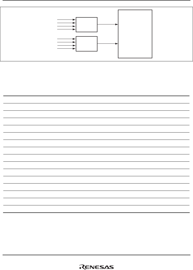
10. Interrupt Controller (INTC)
Rev.1.00 Jan. 10, 2008 Page 326 of 1658
REJ09B0261-0100
Priority
encoder
Interrupt
requests
SH7785
IRQ/IRL3 to
IRQ/IRL0
IRQ/IRL7 to
IRQ/IRL4
IRL7 to IRL4
IRL3 to IRL0
Interrupt
requests
Priority
encoder
Figure 10.3 Example of IRL Interrupt Connection
Table 10.12 IRL Interrupt Pins (IRL[3:0], IRL[7:4]) and Interrupt Levels
IRL3 or
IRL7
IRL2 or
IRL6
IRL1 or
IRL5
IRL0 or
IRL4
Interrupt
Priority Level Interrupt Request
Low Low Low Low 15 Level 15 interrupt request
Low Low Low High 14 Level 14 interrupt request
Low Low High Low 13 Level 13 interrupt request
Low Low High High 12 Level 12 interrupt request
Low High Low Low 11 Level 11 interrupt request
Low High Low High 10 Level 10 interrupt request
Low High High Low 9 Level 9 interrupt request
Low High High High 8 Level 8 interrupt request
High Low Low Low 7 Level 7 interrupt request
High Low Low High 6 Level 6 interrupt request
High Low High Low 5 Level 5 interrupt request
High Low High High 4 Level 4 interrupt request
High High Low Low 3 Level 3 interrupt request
High High Low High 2 Level 2 interrupt request
High High High Low 1 Level 1 interrupt request
High High High High 0 No interrupt request
IRL interrupt detection requires an on-chip noise-cancellation feature. This detection is performed
when the level sampled at every bus clock is the same for three consecutive cycles. This detection
can prevent the incorrect level from being taking in when the IRL interrupt pin state changes.

10. Interrupt Controller (INTC)
Rev.1.00 Jan. 10, 2008 Page 327 of 1658
REJ09B0261-0100
The priority of IRL interrupts should be retained from when an interrupt is accepted to when
interrupt handling starts. The level can be changed to a higher level.
When the INTMU bit in CPUOPM is set to 1, the interrupt mask level (IMASK) bit in SR is
automatically set to the level of the accepted interrupt. When the INTMU bit in CPUOPM is
cleared to 0, the IMASK bit in SR is not affected.
When 1 is written to the IRLM0 and IRLM1 bits in ICR0, pins IRQ/IRL0 to IRQ/IRL3 or
IRQ/IRL7 to IRQ/IRL4 can be used for independent IRQ interrupts. For details, see section
10.4.2, IRQ Interrupts.
(2) Dependence on ICR0.LVLMODE Setting
(a) ICR0.LVLMODE = 0
After an IRL interrupt request is detected, the IRL interrupt with the highest priority is retained in
the following cases until the CPU accepts an interrupt (including other interrupts). The cases are
where the interrupt request is withdrawn or where the priority is set lower.
To clear the retained IRL interrupt source, change the pin state of IRL interrupts by interrupt
routine and withdraw the interrupt request. The, clear the corresponding interrupt mask bit to 1
(To clear the IRL interrupt request by pins IRQ/IRL3 to IRQ/IRL0, write 1 to the IM10 bit in
INTMSK1. To clear the IRL interrupt request by pins IRQ/IRL7 to IRQ/IRL4, write 1 to the IM11
bit in INTMSK1. The IRL interrupt source being detected cannot be cleared even if the masking is
performed in INTMSK2 by the level.).
(b) ICR0.LVLMODE = 1
The INTC does not retain the IRL interrupt source.
10.4.4 On-Chip Peripheral Module Interrupts
On-chip module interrupts are interrupts generated in the on-chip modules.
The interrupt vectors are not allocated to each source, but the source is reflected on INTEVT.
Therefore, the source can be easily identified by branching the value of INTEVT as offset during
exception handling routine.
A priority ranging from 31 to 0 can be set for each module by INT2PRI0 to INT2PRI9. To notify
the CPU of the priority, round down the least 1-bit and change to 4 bits. For details, see section
10.4.5, Priority of On-Chip Peripheral Module Interrupts.

10. Interrupt Controller (INTC)
Rev.1.00 Jan. 10, 2008 Page 328 of 1658
REJ09B0261-0100
An on-chip peripheral module interrupt source flag or an interrupt enable flag should be updated
when the BL bit in SR is set to 1 or when the corresponding interrupt is not generated by the
setting of interrupt masking occurs. To prevent the acceptance of incorrect interrupts by the
updated interrupt source, read from the on-chip peripheral module register that has the
corresponding flag. Then, clear the BL bit to 0 or update the interrupt masking setting so that the
corresponding interrupt can be accepted, after waiting for the on-chip peripheral module priority
determination time specified by table 10.14, Interrupt Response Time (for example, read from a
register operating with the peripheral module clock in the INTC). These procedures can guarantee
the required timing. To update multiple flag, read from the register that has the last flag after
updating the flag.
If a flag is updated when the BL bit is 0, the processing may skip to interrupt processing routine
with the INTEVT value cleared to 0. This is because interrupt processing starts, relative to the
timing that the flag is updated and the interrupt request is identified in this LSI. The processing
can be continued successfully by executing the RTE instruction.
Note that the GPIO interrupt is a low-active interrupts. Unlike the IRL interrupt and the IRQ
interrupt that is detected by the level detection, the GPIO interrupt source cannot be retained by
hardware if the pin state is changed and the interrupt request is withdrawn.
10.4.5 Priority of On-Chip Peripheral Module Interrupts
When any interrupt is generated, the on-chip peripheral module interrupt outputs the exception
code specific to the source to SH-4A. Accepting the interrupt, Sh-4A indicates the corresponding
INTEVT code in INTEVT. An interrupt handler can identify the source by reading from INTEVT
in SH-4A, without reading the source indicate register in the INTC. For the correspondence
between on-chip peripheral module interrupt sources and exception codes, see table 10.1.
As shown in figure 10.4, an on-chip module interrupt source can be set to 30 levels (H'00 and H'01
mask interrupt requests) by the 5-bit field. The interrupt level receive interface in SH-4A can be
set to 15 levels (H'0 masks interrupt requests) by the 4-bit field. The priority of on-chip peripheral
module interrupts is determined by selecting each interrupt source with 5 bits that are extended 1
bit. Then, change 4 bits that round down the least 1 bit and notifies. For example, two interrupt
sources with priority levels set to H'1A and H'1B will both be output to the CPU as the 4-bit
priority level H'D. The two interrupt sources have the same priority value. However, although the
rounded codes are the same for both interrupt sources, the interrupt with priority level H'1B
clearly has priority when we consider the 5-bit data in the priority setting. That is, the 5-bit values
in the fields give INTC a way to differentiate between interrupts with the same four-bit priority
level. If the interrupts of the same priority coinside, the INTEVT code is notified according to the
priority shown in table 10.13.
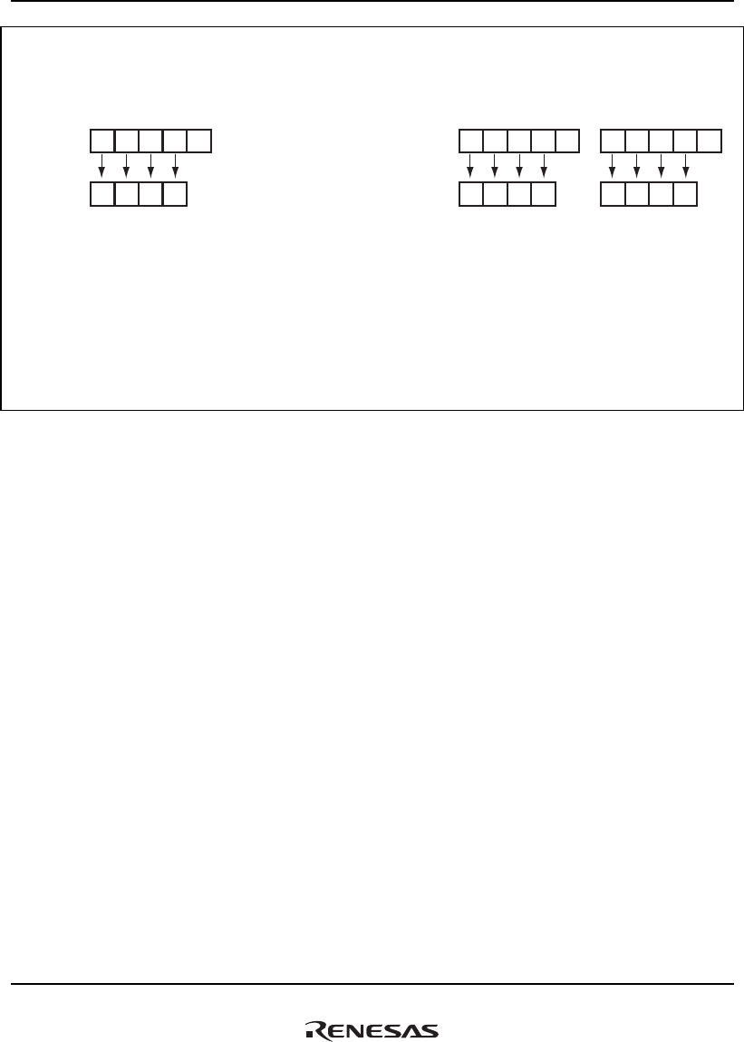
10. Interrupt Controller (INTC)
Rev.1.00 Jan. 10, 2008 Page 329 of 1658
REJ09B0261-0100
An interrupt request is masked if priority level H'01 is set. INTC distinguishes between priority levels H'1A and H'1B,
although both become the same level after truncating the
least significant bit for the CPU.
INTC
Priority level: higher (H'1B) lower (H'1A)
CPU
Priority level: Regarded as the same level (H'D)
If multiple interrupt requests from on-chip modules
occur simultaneously, the INTC processes the interrupt with
the higher priority level (H'1B in the above case).
However, if an external interrupt request is also generated
at the same time the external interrupt request will have
higher priority in the following cases:
- an NMI interrupt request
- an IRQ or IRL interrupt request that has the same or
higher priority level (H'D or greater in the above case).
INTC
Priority level: H'01
CPU
Priority level: H'0 (interrupt is masked)
Priority level H'01 becomes H'00 after the least significant
bit is truncated, so the CPU is not notified of the
corresponding interrupt. The range of priority levels in
the interrupt priority register thus H'02 to H'1F
(30 priority levels).
1101
1101
1 1101
1101
00 0 0 0
0 0 0 0
1
Figure 10.4 Priority of On-Chip Peripheral Module Interrupts
10.4.6 Interrupt Exception Handling and Priority
Table 10.13 shows the interrupt source, codes for INTEVT, and the order of interrupt priority.
A unique INTEVT code is allocated to each interrupt source. The start address of the exception
handling routine is the same for all of the interrupt sources. Therefore, the INTEVT value is used
to control branching at the start of the exception handling routine. For instance, the INTEVT
values are used to branch to offsets.
The priority of the on-chip modules is arbitrarily specified by setting values from 31 to 2 in
INT2PRI0 to INT2PRI7. The priority values for the on-chip modules are set to 0 by a reset.
When interrupt sources share the same priority level and are generated simultaneously, they are
handled according to the default priority order given in table 10.13.
Values of INTPRI and INT2PRI0 to INT2PRI7 should only be updated when the BL bit in SR is
set to 1. To prevent erroneous interrupt acceptance, only clear the BL bit to 0 after having read one
of the interrupt priority level-setting registers. This guarantees the necessary timing internally.

10. Interrupt Controller (INTC)
Rev.1.00 Jan. 10, 2008 Page 330 of 1658
REJ09B0261-0100
Table 10.13 Interrupt Exception Handling and Priority
Interrupt Source
INTEVT
Code
Interrupt
Priority
Mask/Clear
Register & Bit
Interrupt
Source
Register
Detail
Source
Register
Priority
within
Sets of
Sources
Default
Priority
NMI ⎯ H'1C0 16 ⎯ ⎯ ⎯ High
IRL[3:0] = LLLL (H'0) H'200 15 INTMSK2[31]
INTMSKCLR2[31]
⎯ ⎯ High
IRL[7:4] = LLLL (H'0) H'B00 INTMSK2[15]
INTMSKCLR2[15]
⎯ ⎯ Low
IRL[3:0] = LLLH (H'1) H'220 14 INTMSK2[14]
INTMSKCLR2[14]
⎯ ⎯ High
IRL[7:4] = LLLH (H'1) H'B20 INTMSK2[30]
INTMSKCLR2[30]
⎯ ⎯ Low
IRL[3:0] = LLHL (H'2) H'240 13 INTMSK2[13]
INTMSKCLR2[13]
⎯ ⎯ High
IRL[7:4] = LLHL (H'2) H'B40 INTMSK2[29]
INTMSKCLR2[29]
⎯ ⎯ Low
IRL
L: Low
level
input
H: High
level
input
(See
table
10.11)
IRL[3:0] = LLHH (H'3) H'260 12 INTMSK2[12]
INTMSKCLR2[12]
⎯ ⎯ High
IRL[7:4] = LLHH (H'3) H'B60 INTMSK2[28]
INTMSKCLR2[28]
⎯ ⎯ Low
IRL[3:0] = LHLL (H'4) H'280 11 INTMSK2[11]
INTMSKCLR2[11]
⎯ ⎯ High
IRL[7:4] = LHLL (H'4) H'B80 INTMSK2[27]
INTMSKCLR2[27]
⎯ ⎯ Low
IRL[3:0] = LHLH (H'5) H'2A0 10 INTMSK2[10]
INTMSKCLR2[10]
⎯ ⎯ High
IRL[7:4] = LHLH (H'5) H'BA0 INTMSK2[26]
INTMSKCLR2[26]
⎯ ⎯ Low
IRL[3:0] = LHHL (H'6) H'2C0 9 INTMSK2[9]
INTMSKCLR2[9]
⎯ ⎯ High
IRL[7:4] = LHHL (H'6) H'BC0 INTMSK2[25]
INTMSKCLR2[25]
⎯ ⎯ Low
IRL[3:0] = LHHH (H'7) H'2E0 8 INTMSK2[8]
INTMSKCLR2[8]
⎯ ⎯ High
IRL[7:4] = LHHH (H'7) H'BE0 INTMSK2[24]
INTMSKCLR2[24]
⎯ ⎯ Low
Low

10. Interrupt Controller (INTC)
Rev.1.00 Jan. 10, 2008 Page 331 of 1658
REJ09B0261-0100
Interrupt Source
INTEVT
Code
Interrupt
Priority
Mask/Clear
Register & Bit
Interrupt
Source
Register
Detail
Source
Register
Priority
within
Sets of
Sources
Default
Priority
IRL[3:0] = HLLL (H'8) H'300 7 INTMSK2[7]
INTMSKCLR2[7]
⎯ ⎯ High
High
IRL[7:4] = HLLL (H'8) H'C00 INTMSK2[23]
INTMSKCLR2[23]
⎯ ⎯ Low
IRL[3:0] = HLLH (H'9) H'320 6 INTMSK2[6]
INTMSKCLR2[6]
⎯ ⎯ High
IRL[7:4] = HLLH (H'9) H'C20 INTMSK2[22]
INTMSKCLR2[22]
⎯ ⎯ Low
IRL
L: Low
level
input
H: High
level
input
(See
table
10.11) IRL [3:0] = HLHL (H'A) H'340 5 INTMSK2[5]
INTMSKCLR2[5]
⎯ ⎯ High
IRL[7:4] = HLHL (H'A) H'C40 INTMSK2[21]
INTMSKCLR2[21]
⎯ ⎯ Low
IRL[3:0] = HLHH (H'B) H'360 4 INTMSK2[4]
INTMSKCLR2[4]
⎯ ⎯ High
IRL[7:4] = HLHH (H'B) H'C60 INTMSK2[20]
INTMSKCLR2[20]
⎯ ⎯ Low
IRL[3:0] = HHLL (H'C) H'380 3 INTMSK2[3]
INTMSKCLR2[3]
⎯ ⎯ High
IRL[7:4] = HHLL (H'C) H'C80 INTMSK2[19]
INTMSKCLR2[19]
⎯ ⎯ Low
IRL[3:0] = HHLH (H'D) H'3A0 2 INTMSK2[2]
INTMSKCLR2[2]
⎯ ⎯ High
IRL[7:4] = HHLH (H'D) H'CA0 INTMSK2[18]
INTMSKCLR2[18]
⎯ ⎯ Low
IRL[3:0] = HHHL (H'E) H'3C0 1 INTMSK2[1]
INTMSKCLR2[1]
⎯ ⎯ High
IRL[7:4] = HHHL (H'E) H'CC0 INTMSK2[17]
INTMSKCLR2[17]
⎯ ⎯ Low
Low

10. Interrupt Controller (INTC)
Rev.1.00 Jan. 10, 2008 Page 332 of 1658
REJ09B0261-0100
Interrupt Source
INTEVT
Code
Interrupt
Priority
Mask/Clear
Register & Bit
Interrupt
Source
Register
Detail
Source
Register
Priority
within
Sets of
Sources
Default
Priority
IRQ IRQ[0] H'240 INTPRI
[31:28]
INTMSK0[31]
INTMSKCLR0
[31]
INTREQ
[31]
⎯ High
IRQ[1] H'280 INTPRI
[27:24]
INTMSK0[30]
INTMSKCLR0
[30]
INTREQ
[30]
⎯
IRQ[2] H'2C0 INTPRI
[23:20]
INTMSK0[29]
INTMSKCLR0
[29]
INTREQ
[29]
⎯
IRQ[3] H'300 INTPRI
[19:16]
INTMSK0[28]
INTMSKCLR0
[28]
INTREQ
[28]
⎯
IRQ[4] H'340 INTPRI
[15:12]
INTMSK0[27]
INTMSKCLR0
[27]
INTREQ
[27]
⎯
IRQ[5] H'380 INTPRI
[11:8]
INTMSK0[26]
INTMSKCLR0
[26]
INTREQ
[26]
⎯
IRQ[6] H'3C0 INTPRI
[7:4]
INTMSK0[25]
INTMSKCLR0
[25]
INTREQ
[25]
⎯
IRQ[7] H'200 INTPRI
[3:0]
INTMSK0[24]
INTMSKCLR0
[24]
INTREQ
[24]
⎯
WDT ITI* H'560 INT2PRI3
[12:8]
INT2MSKR[8]
INT2MSKCR[8]
INT2A0[8]
INT2A1[8]
⎯
TMU-ch0 TUNI0* H'580 INT2PRI0
[28:24]
INT2B0[0]
TMU-ch1 TUNI1* H'5A0 INT2PRI0
[20:16]
INT2B0[1]
TMU-ch2 TUNI2* H'5C0 INT2PRI0
[12:8]
INT2B0[2]
TICPI2* H'5E0 INT2PRI0
[4:0]
INT2MSKR[0]
INT2MSKCLR
[0]
INT2A0[0]
INT2A1[0]
INT2B0[3]
H-UDI H-UDII H'600 INT2PRI4
[28:24]
INT2MSKR[9]
INT2MSKCLR
[9]
INT2A0[9]
INT2A1[9]
⎯
Low
10. Interrupt Controller (INTC)
Rev.1.00 Jan. 10, 2008 Page 333 of 1658
REJ09B0261-0100
Interrupt Source
INTEVT
Code
Interrupt
Priority
Mask/Clear
Register & Bit
Interrupt
Source
Register
Detail
Source
Register
Priority
within
Sets of
Sources
Default
Priority
DMAC(0) DMINT0* H'620 INT2B3[0]
High High
DMINT1* H'640 INT2B3[1]
DMINT2* H'660
INT2PRI4
[20:16]
INT2MSKR[10]
INT2MSKCLR
[10]
INT2A0[10]
INT2A1[10]
INT2B3[2]
DMINT3* H'680 INT2B3[3]
DMINT4* H'6A0 INT2B3[4]
DMINT5* H'6C0 INT2B3[5]
DMAE (ch0 to ch5)* H'6E0 INT2B3[6] Low
SCIF-ch0 ERI0* H'700 INT2B2[0]
High
RXI0* H'720
INT2PRI2
[28:24]
INT2MSKR[2]
INT2MSKCLR[2]
INT2A0[2]
INT2A1[2] INT2B2[1]
BRI0* H'740 INT2B2[2]
TXI0* H'760 INT2B2[3] Low
SCIF-ch1 ERI1* H'780 INT2B3[4]
High
RXI1* H'7A0
INT2PRI2
[20:16]
INT2MSKR[3]
INT2MSKCLR[3]
INT2A0[3]
INT2A1[3] INT2B3[5]
BRI1* H'7C0 INT2B3[6]
TXI1* H'7E0
INT2B3[7] Low
DMAC(1) DMINT6* H'880 INT2B2[7]
DMINT7* H'8A0 INT2B2[8]
DMINT8* H'8C0
INT2PRI4
[12:8]
INT2MSKR[11]
INT2MSKCLR
[11]
INT2A0[11]
INT2A1[11]
INT2B2[9]
DMINT9* H'8E0 INT2B2[10]
DMINT10* H'900 INT2B3[11]
DMINT11* H'920 INT2B3[12]
DMAE (ch6 to
ch11)*
H'940 INT2B3[13]
HSPI SPII H'960 INT2PRI7
[20:16]
INT2MSKR[21]
INT2MSKCLR
[21]
INT2A0[21]
INT2A1[21]
⎯
Low
10. Interrupt Controller (INTC)
Rev.1.00 Jan. 10, 2008 Page 334 of 1658
REJ09B0261-0100
Interrupt Source
INTEVT
Code
Interrupt
Priority
Mask/Clear
Register & Bit
Interrupt
Source
Register
Detail
Source
Register
Priority
within
Sets of
Sources
Default
Priority
SCIF-ch2 ERI2* INT2B1[8] High
RXI2*
H'980 INT2PRI2
[12:8]
INT2MSKR[4]
INT2MSKCLR[4]
INT2A0[4]
INT2A1[4] INT2B1[9]
BRI2* INT2B1[10]
TXI2* INT2B1[11]
SCIF-ch3 ERI3* INT2B1[12]
RXI3*
H'9A0 INT2PRI2
[4:0]
INT2MSKR[5]
INT2MSKCLR[5]
INT2A0[5]
INT2A1[5] INT2B1[12]
BRI3* INT2B1[14]
TXI3* INT2B1[15]
SCIF-ch4 ERI4* INT2B1[16]
RXI4*
H'9C0 INT2PRI3
[28:24]
INT2MSKR[6]
INT2MSKCLR[6]
INT2A0[6]
INT2A1[6] INT2B1[17]
BRI4* INT2B1[18]
TXI4* INT2B1[19]
SCIF-ch5 ERI5* INT2B1[20]
RXI5*
H'9E0 INT2PRI2
[20:16]
INT2MSKR[7]
INT2MSKCLR[7]
INT2A0[7]
INT2A1[7] INT2B1[21]
BRI5* INT2B1[22]
TXI5* INT2B1[23]
PCIC(0) PCISERR H'A00 INT2PRI5
[12:8]
INT2MSKR[14]
INT2MSKCLR
[14]
INT2A0[14]
INT2A1[14]
INT2B3[0]
PCIC(1) PCIINTA H'A20 INT2PRI5
[4:0]
INT2MSKR[15]
INT2MSKCLR
[15]
INT2A0[15]
INT2A1[15]
INT2B3[1]
PCIC(2) PCIINTB H'A40 INT2PRI6
[28:24]
INT2MSKR[16]
INT2MSKCLR
[16]
INT2A0[16]
INT2A1[16]
INT2B3[2]
PCIC(3) PCIINTC H'A60 INT2PRI6
[20:16]
INT2MSKR[17]
INT2MSKCLR
[17]
INT2A0[17]
INT2A1[17]
INT2B3[3]
PCIC(4) PCIINTD H'A80 INT2PRI6
[12:8]
INT2MSKR[18]
INT2MSKCLR
[18]
INT2A0[18]
INT2A1[18]
INT2B3[4]
Low

10. Interrupt Controller (INTC)
Rev.1.00 Jan. 10, 2008 Page 335 of 1658
REJ09B0261-0100
Interrupt Source
INTEVT
Code
Interrupt
Priority
Mask/Clear
Register & Bit
Interrupt
Source
Register
Detail
Source
Register
Priority
within
Sets of
Sources
Default
Priority
PCIC(5) PCIERR H'AA0 INT2B4[5]
High High
PCIPWD3 H'AC0 INT2B4[6]
PCIPWD2 H'AC0
INT2PRI6
[4:0]
INT2MSKR[19]
INT2MSKCLR
[19]
INT2A0[19]
INT2A1[19]
INT2B4[7]
PCIPWD1 H'AC0 INT2B4[8]
PCIPWD0 H'AE0 INT2B4[9] Low
SIOF SIOFI H'CE0
INT2PRI6
[28:24]
INT2MSKR[20]
INT2MSKCR[20]
INT2A0[20]
INT2A1[20]
⎯
MMCIF FSTAT H'D00 INT2B4[0]
High
TRAN H'D20 INT2B4[1]
ERR H'D40
INT2PRI6
[12:8]
INT2MSKR[22]
INT2MSKCLR
[22]
INT2A0[22]
INT2A1[22]
INT2B4[2]
FRDY H'D60 INT2B4[3] Low
DU DUI H'D80
INT2PRI9
[28:24]
INT2MSKR[27]
INT2MSKCLR
[27]
INT2A0[27]
INT2A1[27]
GDTA GACLI H'DA0 INT2B7[0] High
GAMCI H'DC0 INT2B7[1]
GAERI H'DE0
INT2PRI9
[20:16]
INT2MSKR[28]
INT2MSKCLR
[28]
INT2A0[28]
INT2A1[28]
INT2B7[2] Low
TMU-ch3 TUNI3* H'E00
INT2PRI1
[28:24]
INT2MSKR[1]
INT2MSKCLR[1]
INT2A0[1]
INT2A1[1]
INT2B0[4]
TMU-ch4 TUNI4* H'E20
INT2PRI1
[20:16]
INT2B0[5]
TMU-ch5 TUNI5* H'E40
INT2PRI1
[12:8]
INT2B0[6]
SSI-ch0 SSII0 H'E80 INT2PRI8
[12:8]
INT2MSKR[25]
INT2MSKCLR
[25]
INT2A0[25]
INT2A1[25]
⎯
SSI-ch1 SSII1 H'EA0 INT2PRI6
[4:0]
INT2MSKR[26]
INT2MSKCLR
[26]
INT2A0[26]
INT2A1[26]
⎯
HAC-ch0 HACI0 H'EC0 INT2PRI6
[28:24]
INT2MSKR[12]
INT2MSKCLR
[12]
INT2A0[12]
INT2A1[12]
⎯
Low
10. Interrupt Controller (INTC)
Rev.1.00 Jan. 10, 2008 Page 336 of 1658
REJ09B0261-0100
Interrupt Source
INTEVT
Code
Interrupt
Priority
Mask/Clear
Register & Bit
Interrupt
Source
Register
Detail
Source
Register
Priority
within
Sets of
Sources
Default
Priority
HAC-ch1 HACI1 H'EE0 INT2PRI6
[20:16]
INT2MSKR[13]
INT2MSKCLR
[13]
INT2A0[13]
INT2A1[13]
⎯
FLCTL FLSTE* H'F00 INT2B5[0]
High
High
FLTEND* H'F20
INT2PRI8
[28:24]
INT2MSKR[23]
INT2MSKCR[23]
INT2A0[23]
INT2A1[23] INT2B5[1]
FLTRQ0* H'F40 INT2B5[2]
FLTRQ1* H'F60 INT2B5[3] Low
GPIO GPIOI0 (Port E0) H'F80 INT2B6[0]
High
GPIOI0 (Port E1)
INT2MSKR[24]
INT2MSKCR[24]
INT2A0[24]
INT2A1[24] INT2B6[1]
GPIOI0 (Port E2)
INT2PRI8
[20:16]
INT2B6[2]
GPIOI1 (Port E3) H'FA0 INT2B6[8]
GPIOI1 (Port E4) INT2B6[9]
GPIOI1 (Port E5) INT2B6[10]
GPIOI2 (Port H1) H'FC0 INT2B6[16]
GPIOI2 (Port H2) INT2B6[17]
GPIOI2 (Port H3) INT2B6[18]
GPIOI2 (Port H4) INT2B6[19]
GPIOI3 (Port L6) H'FE0 INT2B6[24]
GPIOI3 (Port L7) INT2B6[25] Low Low
Note: * ITI: Interval timer interrupt
TUNI0 to TUNI5: TMU channels 0 to 5 under flow interrupt
TICPI2: TMU channel 2 input capture interrupt
DMINT0 to DMINT11: Transfer end or half-end interrupts for DMAC channel 0 to 11
DMAE0: DMAC address error interrupt (channels 0 to 5)
DMAE1: DMAC address error interrupt (channels 6 to 11)
ERI0, ERI1, ERI2, ERI3, ERI4, ERI5: SCIF channels 0 to 5 receive error interrupts
RXI0, RXI1, RXI2, RXI3, RXI4, RXI5: SCIF channels 0 to 5 receive data full interrupts
BRI0, BRI1, BRI2, BRI3, BRI4, BRI5: SCIF channels 0 to 5 break interrupts
TXI0, TXI1, TXI2, TXI3, TXI4, TXI5: SCIF channels 0 to 5 transmission data empty
interrupts
FLSTE: FLCTL error interrupt
FLTEND: FLCTL error interrupt
FLTRQ0: FLCTL data FIFO transfer request interrupt
FLTRQ1: FLCTL control code FIFO transfer request interrupt

10. Interrupt Controller (INTC)
Rev.1.00 Jan. 10, 2008 Page 337 of 1658
REJ09B0261-0100
10.5 Operation
10.5.1 Interrupt Sequence
The sequence of interrupt operations is described below. Figure 10.4 shows a flowchart of the
operations.
1. Interrupt request sources send interrupt request signals to the INTC.
2. The INTC selects the interrupt with the highest priority among the interrupts that have been
sent, according to the priority set in INTPRI and INT2PRI0 to INT2PRI9. Lower priority
interrupts are held as pending interrupts. If two of the interrupts have the same priority level or
multiple interrupts are generated by a single module, the interrupt with the highest priority is
selected according to table 10.13.
3. The priority level of the interrupt selected by the INTC is compared with the interrupt mask
level (IMASK) set in SR of the CPU. Only the interrupt with a higher priority than the IMASK
bit is accepted, and an interrupt request signal is sent to the CPU.
4. The CPU accepts an interrupt at the next break between instructions.
5. The interrupt source code is set in the interrupt event register (INTEVT).
6. The SR and program counter (PC) are saved in SSR and SPC, respectively. At that time, R15
is saved in SGR.
7. The BL, MD, and RB bits in SR are set to 1.
8. Execution jumps to the start address of the interrupt exception handling routine (the sum of the
value set in the vector base register (VBR) and H'0000 0600).
In the exception handling routine, the value of INTEVT is branched as an offset. This easily
enables to branch the exception handling routine to handling routine for each interrupt source.
Notes: 1. When the INTMU bit in CPUOPM is set to 1, the interrupt mask level (IMASK) in SR
is automatically set to the level of the accepted interrupt. When the INTMU bit in
CPUOPM is cleared to 0, the value of the IMASK in SR is not affected by the accepted
interrupt.
2. The interrupt source flag should be cleared during exception handling routine. To
ensure that an interrupt source which should have been cleared is not erroneously
accepted again, read the interrupt source flag after it has been cleared, and wait for the
time shown in table 10.14. Then, clear the BL bit or execute an RTE instruction.
3. The IRQ interrupts, IRL interrupts, on-chip peripheral module interrupts are initialized
to the interrupt masking state by a power-on reset. Therefore, clear the interrupt
masking for each interrupt , INTMSK0, INTMSK1, and INT2MSKR by using
INTMSKCLR0, INTMSKCLR1, and INT2MSKCLR.
10. Interrupt Controller (INTC)
Rev.1.00 Jan. 10, 2008 Page 338 of 1658
REJ09B0261-0100
Program execution state
Interrupt
generated?
ICR0.MAI = 1?
SR.BL = 0 or
sleep mode?
Yes
Yes
Yes
Yes
Yes Yes
Yes
Yes
Yes
Yes
Yes
Yes
No
No
No
No
No
No
No
No
NMI?
No
Yes
No
No
Yes
Is NMI input low?
Level 15
interrupt?
No
No
No
Set interrupt source
code in INTEVT
Save SR in SSR;
save PC in SPC;
save R15 in SGR
Set SR.IMASK to
accepted interrupt level
Branch to
exception handling routine
Is SR.IMASK level
14 or less?
Level 14
interrupt?
Level 1
interrupt?
NMI?
Is SR.IMASK level
13 or less?
Is SR.IMASK level
0?
ICR0.NMIB = 1?
CPUOPM.INTMU = 1?
Figure 10.5 Flowchart of Interrupt Operation

10. Interrupt Controller (INTC)
Rev.1.00 Jan. 10, 2008 Page 339 of 1658
REJ09B0261-0100
10.5.2 Multiple Interrupts
To handle multiple interrupts, the procedure for the interrupt handling routine should be as
follows.
1. To identify the interrupt source, set the value of INTEVT to an offset and branch it to the
interrupt handling routine for each interrupt source.
2. Clear the corresponding interrupt source in the interrupt handling routine.
3. Save SSR and SPC on the stack.
4. Clear the BL bit in SR. When the INTMU bit in CPUOPM is set to 1, the interrupt mask level
(IMASK) in SR is automatically set to the level of the accepted interrupt. When the INTMU
bit in CPUOPM is cleared to 0, software should be used to set the IMASK bit in SR to the
priority level of the accepted interrupt.
5. Execute processing as required in response to the interrupt.
6. Set the BL bit in SR to 1.
7. Release SSR and SPC from the stack.
8. Execute the RTE instruction.
By following the above procedure, if further interrupts are generated right after step 4, an interrupt
with higher priority than the one currently being handled can be accepted after step 4. This reduces
the interrupt response time for urgent processing.
10.5.3 Interrupt Masking by MAI Bit
When the MAI bit in ICR0 is set to 1, interrupts can be masked whole the NMI pin is low
regardless of the settings of the BL and IMASK bits in and SR.
• Normal operation or sleep mode
All other interrupts are masked while the NMI signal is low. Note that only NMI interrupts due to
the change of the NMI pin are generated.

10. Interrupt Controller (INTC)
Rev.1.00 Jan. 10, 2008 Page 340 of 1658
REJ09B0261-0100
10.6 Interrupt Response Time
Table 10.14 shows response time. The response time is the interval from generation of an interrupt
request until the start of interrupt exception handling and until fetching of the first instruction of
the exception handling routine.
Table 10.14 Interrupt Response Time
Number of States
Peripheral Modules
Item NMI IRL IRQ
Other than
GPIO/PCIC GPIO/PCIC Remarks
Priority
determination time
6Bcyc +
2Pcyc
8Bcyc +
2Pcyc
4Bcyc +
2Pcyc
5Pcyc 7Pcyc
Wait time until the
CPU finishes the
current sequence
S-1 (≥ 0)
× Icyc
Interval from the
start of interrupt
exception handling
(saving SR and PC)
until a SuperHyway
bus request is issued
to fetch the first
instruction of the
exception handling
routine
11Icyc
+ 1Scyc
Response
time
Total (S + 10) Icyc
+ 1Scyc
+ 5Bcyc
+ 2Pcyc
(S + 10) Icyc
+ 1Scyc
+ 8Bcyc
+ 2Pcyc
(S + 10) Icyc
+ 1Scyc
+ 4Bcyc
+ 2Pcyc
(S + 10) Icyc
+ 1Scyc
+ 5Pcyc
(S + 10) Icyc
+ 1Scyc
+ 7Pcyc
Legend:
Icyc: Period of one CPU clock cycle
Scyc: Period of one SuperHyway clock cycle
Bcyc: Period of one bus clock cycle
Pcyc: Period of one peripheral clock cycle
S: Number of instruction execution states

10. Interrupt Controller (INTC)
Rev.1.00 Jan. 10, 2008 Page 341 of 1658
REJ09B0261-0100
Table 10.15 shows response time. The response time is from the interrupt exception handling to
the start of fetching the first instruction in exception handling routine. In this case, suppose that
the setting values of the following registers that enable or disable interrupt, INTMSK0,
INTMSK1, INTMSK2, INT2MSKR, and INT2GPIC, are changed from the interrupt disable state
to the interrupt enable state.
Table 10.15 Response Time after Changing the Value of Interrupt Enable/Disable Registers
(Interrupt Disabled → Interrupt Enabled)
Number of States
IRL IRQ
Peripheral
Modules Remarks
Item INTMSK1 INTMSK2 INTMSK0
INT2MSKR,
INT2GPIC
Registers that
enable/disable
interrupts
Priority determination time* 1Pcyc 8Bcyc +
2Pcyc
1Pcyc 4Pcyc
Wait time until the CPU
finishes the current sequence
S-1 (≥ 0) × Icyc
Interval from the start of
interrupt exception handling
(saving SR and PC) until a
SuperHyway bus request is
issued to fetch the first
instruction of the exception
handling routine
11Icyc + 1Scyc
Response
time
Total (S + 10) Icyc
+ 1Scyc
+ 1Pcyc
(S + 10) Icyc
+ 1Scyc
+ 8Bcyc
+ 2Pcyc
(S + 10) Icyc
+ 1Scyc
+ 1Pcyc
(S + 10) Icyc
+ 1Scyc
+ 4Pcyc
Legend:
Icyc: Period of one CPU clock cycle
Scyc: Period of one SuperHyway clock cycle
Bcyc: Period of one bus clock cycle
Pcyc: Period of one peripheral clock cycle
S: Number of instruction execution states
Note: * When INTMSKCLR0, INTMSKCLR1, INTMSKCLR2, and INT2MSKCLR are written to,
INTMSK0, INTMSK1, INTMSK2, and INTMSKR enable an interrupt by clearing the
mask bits in INTMSK0, INTMSK1, INTMSK2, and INTMSKR. The priority determination
times in table 10.15 are the values after the values of INTMSK0, INTMSK1, INTMSK2,
and INT2MSKR are changed.

10. Interrupt Controller (INTC)
Rev.1.00 Jan. 10, 2008 Page 342 of 1658
REJ09B0261-0100
Table 10.16 shows response time. The response time is the time until when the interrupt request
signal from the INTC to the CPU is negated. In this case, suppose that the setting values of the
following registers, INTMSK0, INTMSK1, INTMSK2, INT2MSKR, and INT2GPIC, are changed
from the interrupt enable state to the interrupt disable state.
Table 10.16 Response Time after Changing the Value of Interrupt Enable/Disable Registers
(Interrupt Enabled → Interrupt Disabled)
Number of States
IRL IRQ
Peripheral
Modules Remarks
Item INTMSK1 INTMSK2 INTMSK0
INT2MSKR,
INT2GPIC
Registers that
enable/disable
interrupts
Priority
determination
time
1Pcyc 8Bcyc +
2Pcyc*
1Pcyc 4Pcyc
Note: * The IRL interrupt source that has been already retained inside cannot cancel the
interrupt request signal to the CPU even if the IRL interrupt source is masked.
10. Interrupt Controller (INTC)
Rev.1.00 Jan. 10, 2008 Page 343 of 1658
REJ09B0261-0100
10.7 Usage Notes
10.7.1 Example of Handing Routine of IRL Interrupts and Level Detection IRQ
Interrupts when ICR0.LVLMODE = 0
When ICR0.LVLMODE is 0, IRL interrupt requests and level detection IRQ interrupt requests
that the INTC retains should be cleared in the interrupt handling routine because the CPU detects
after accepting interrupts. The IRQ interrupt sources (INTREQ) should also be cleared.
Interrupt handling
Instruct the external device to cancel
the IRQ/IRL level interrupt request by
using the GPIO output or writing to an
address in the local bus
Clear the IRQ/IRL level interrupt
request holding in the detection circuit
and clear the IRQ interrupt source
End of IRQ/IRL level
interrupt handling
1) Write to the GPIO register or local
bus space.
2) Read from the address that has been
written to.
1) Set the corresponding bit in
INTMSK0/1 to 1.
2) Set the corresponding bit in
INTMSKCLR0/1 to 1.
3) Read INTMSK0/1.
Start of IRQ level-sense or IRL
level-encoded interrupt handling
Wait until the interrupt request signal
input on the IRL/IRQ pin is negated
and the INTC detects the negation
(at least 8 bus-clock cycles are
required)
Figure 10.6 Example of Interrupt Handling Routine
Canceling the IRL interrupt request and level detection IRQ interrupt request that the CPU accepts
should be notified to the external device in the interrupt handling routine. For example, output the
data that can identify the accepted level and pins to the GPIO pin, or read the specific address. In
this case, write to the GPIO register and the local bus space, and read the same address
continuously.
To clear an interrupt request that is retained in the INTC, the wait time that the CPU detects the
cleared interrupt request is required. To guarantee the wait time, write to INTMSK0, INTMSK1,
INTMSKCLR0, and INTMSKCLR1, and read from INTMSK0 continuously.

10. Interrupt Controller (INTC)
Rev.1.00 Jan. 10, 2008 Page 344 of 1658
REJ09B0261-0100
10.7.2 Notes on Setting IRQ/IRL[7:0] Pin Function
When the IRQ/IRL[7:0] pin functions are switched, the INTC may retain an incorrectly detected
interrupt request. Therefore, mask the IRL and IRQ interrupt requests before switching the
IRQ/IRL[7:0] pin functions.
Table 10.17 Switching Sequence of IRQ/IRL[7:0] Pin Function
Sequence Item Procedure
1 IRL interrupt request and IRQ interrupt
request masking
Write 1 to all bits in INTMSK0 and
INTMSK1 except reserved bits
2 Setting IRL/IRQ[7:4] pins to IRL7 to IRL4 Write 0 to the PMSEL14 bit in PMSELR
Write 0 to the PL4MD1, PL4MD0,
PL3MD1, PL3MD0, PL2MD1, PL2MD0,
PL1MD1, PL1MD0 bits in PLCR
3 Setting IRQ/IRL[7:0] pins to IRL or IRQ Set bits IRLM1 to IRLM0 in ICR0
4 Start of IRL and IRQ interrupt detection Write 1 to the corresponding bit in
INTMSKCLR0 and INTMSKCLR1

10. Interrupt Controller (INTC)
Rev.1.00 Jan. 10, 2008 Page 345 of 1658
REJ09B0261-0100
10.7.3 Clearing IRQ and IRL Interrupt Requests
To clear the interrupt request retained in the INTC, follow the procedure below.
(1) Clearing Interrupt Request Independent from ICR0.LVLMODE Setting
⎯ Clearing IRQ interrupt requests at edge detection
To clear the interrupt requests IRQ7 to IRQ0 setting edge detection, read the IR7 to IR0
bits corresponding to INTREQ as 1 and write 0 to the bits. The IRQ interrupt request
being detected cannot be cleared even if 1 is written to the corresponding bit in
INTMSK0.
(2) Clearing Interrupt Request Dependent on ICR0.LVLMODE Setting
(a) ICR0.LVLMODE = 0
⎯ Clearing IRL interrupt requests
To clear the IRL interrupt requests from the IRQ/IRL[3:0] pins, write 1 to the IM10 bit
in INTMSK1. To clear the IRL interrupt requests from the IRQ/IRL[7:4] pins, write 1 to
the IM11 bit in INTMSK1. The IRL interrupt request being detected cannot be cleared
even if masking is performed on INTMSK2 by the level.
⎯ Clearing IRQ interrupt requests at level detection
To clear the IRQ7 to IRQ0 interrupt request setting level detection, write 1 to the
corresponding IM07 to IM00 bits in INTMSK0. The IRQ interrupt request being
detected cannot be cleared even if 0 is written to the corresponding bit in INTPRI. The
IRQ interrupt request being detected can be checked by reading from INTREQ.
(b) ICR0.LVLMODE = 1
The INTC does not retain the interrupt source even if IRQ interrupts are detected at level detection
or IRL interrupt requests are detected.

10. Interrupt Controller (INTC)
Rev.1.00 Jan. 10, 2008 Page 346 of 1658
REJ09B0261-0100

11. Local Bus State Controller (LBSC)
Rev.1.00 Jan. 10, 2008 Page 347 of 1658
REJ09B0261-0100
Section 11 Local Bus State Controller (LBSC)
The local bus state controller (LBSC) divides the external memory space and outputs control
signals according to the specification of each memory and bus interface. The LBSC function
enables connection of the SRAM or ROM, etc. to this LSI. The LBSC also supports the PCMCIA
interface protocol, which implements simple system design and high-speed data transfers in a
compact system.
11.1 Features
The LBSC has the following features.
• Manages areas 0 to 6 of the external memory space divided into seven
⎯ Maximum 64 Mbytes for each of areas 0 to 6
⎯ Bus width of each area can be set by a register (Only the area-0 bus width is set by an
external pin.)
⎯ Wait cycle insertion by the RDY pin
⎯ Wait cycle insertion can be controlled by a program
⎯ Type of memory to be connected is specifiable for each area
⎯ Control signals are output for memory connected to each area
⎯ Automatic wait cycle insertion to prevent data bus collision in consecutive memory
accesses
⎯ The write strobe setup and hold time periods can be inserted in a write cycle to connect to
low-speed memory
• SRAM interface
⎯ Wait cycle insertion can be controlled by a program
Connectable area: 0 to 6
Settable bus width: 64, 32, 16 and 8 bits
• Burst ROM interface
⎯ Wait cycle insertion can be controlled by a program
⎯ Burst transfers for the number of times specified by the register
Connectable area: 0 to 6
Settable bus width: 64, 32, 16 and 8 bits

11. Local Bus State Controller (LBSC)
Rev.1.00 Jan. 10, 2008 Page 348 of 1658
REJ09B0261-0100
• MPX interface
⎯ Address/data multiplexing
Connectable area: 0 to 6
Settable bus width: 64 and 32 bits
• Byte control SRAM interface
⎯ SRAM interface with byte control
Connectable area: 1 and 4
Settable bus width: 64, 32 and 16 bits
• PCMCIA interface (Little endian only)
⎯ Wait cycle insertion can be controlled by a program
⎯ Bus sizing function for I/O bus width
⎯ Supports the little endian
Connectable area: 5 and 6
Settable bus width: 16 and 8 bits
⎯ Prepared only for ATA device accesses
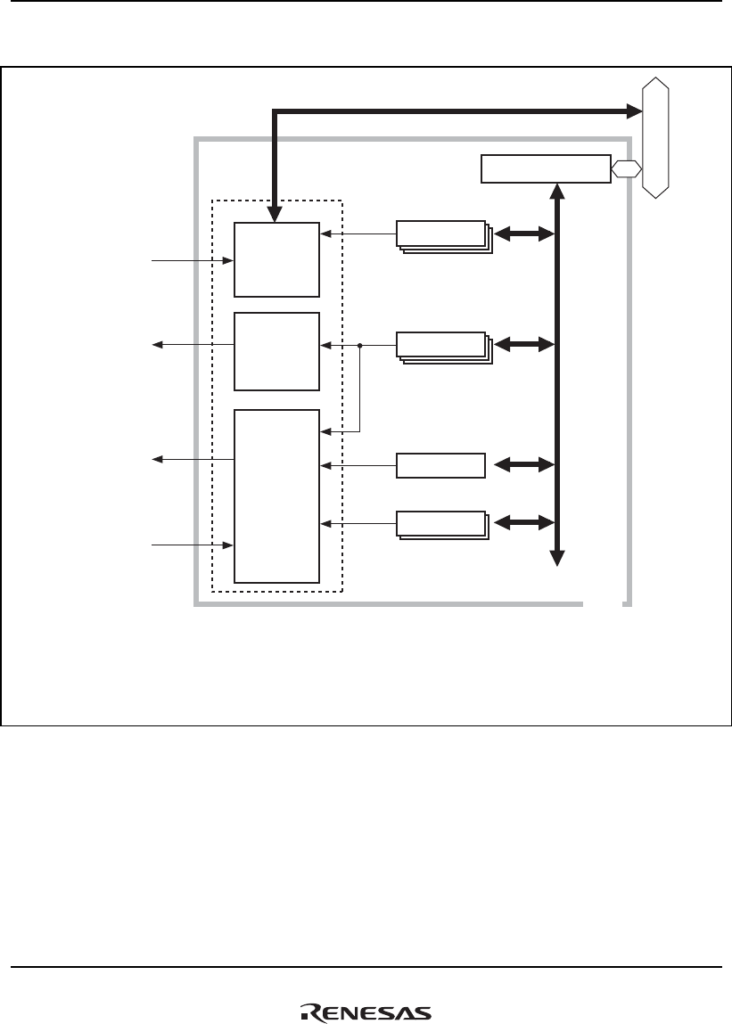
11. Local Bus State Controller (LBSC)
Rev.1.00 Jan. 10, 2008 Page 349 of 1658
REJ09B0261-0100
Figure 11.1 shows a block diagram of the LBSC.
Bus interface
CSnWCR
CSnBCR
BCR
CSnPCR
Memory
controller
Area controller
Wait controller
LBSC
SuperHyway bus
Module bus
RDY
CS0 to CS6
CE2A to CE2B
BS
RD
R/W
WE7 to WE0
IORD, IOWR
REG
IOIS16
Legend:
CSnWCR: CSn wait control register (n = 0 to 6)
CSnBCR: CSn bus control register (n = 0 to 6)
BCR: Bus control register
CSnPCR: CSn PCMCIA control register (n = 5 and 6)
... ...
Figure 11.1 Block Diagram of LBSC

11. Local Bus State Controller (LBSC)
Rev.1.00 Jan. 10, 2008 Page 350 of 1658
REJ09B0261-0100
11.2 Input/Output Pins
Table 11.1 shows the LBSC pin configuration.
Table 11.1 Pin Configuration
Pin Name Function I/O Description
A25 to A0 Address Bus O Address output
D63 to D0 Data Bus I/O Data input/output
These pins are multiplexed as follows:
D63 to D56: PCI, DU and ports A7 to A0 (GPIO
input/output)
D55 to D48: PCI, DU and ports B7 to B0 (GPIO
input/output)
D47 to D40: PCI, DU and ports C7 to C0 (GPIO
input/output)
D39 to D32: PCI, DU and ports D7 to D0 (GPIO
input/output)
D31 to D24: ports F7 to F0 (GPIO input/output)
D23 to D16: ports G7 to G0 (GPIO input/output)
BS Bus Cycle Start O Signal that indicates the start of a bus cycle
Asserted once for a burst transfer when the MPX
interface is set
Asserted in every data cycle in other burst
transfers
CS6 to CS0 Chip Select 6 to
0
O Chip select signals that indicates the area being
accessed. CS5 and CS6 can also be used as
CE1A and CE1B of the PCMCIA respectively.
R/W Read/Write O Data bus input/output direction designation
signal. Also used as the PCMCIA interface write
designation signal
RD/FRAME Read/Cycle
Frame
O Strobe signal indicating a read cycle.
Used for FRAME signal when the MPX bus is
used

11. Local Bus State Controller (LBSC)
Rev.1.00 Jan. 10, 2008 Page 351 of 1658
REJ09B0261-0100
Pin Name Function I/O Description
WE0/REG Data Enable 0 O Write strobe signal for D7 to D0 in SRAM
interface setting
REG signal in PCMCIA interface setting
WE1 Data Enable 1 O Write strobe signal for D15 to D8 in SRAM
interface setting
Write strobe signal in PCMCIA interface setting
WE2/IORD Data Enable 2 O Write strobe signal for D23 to D16 in SRAM
interface setting
IORD signal in PCMCIA interface setting
WE3/IOWR Data Enable 3 O Write strobe signal for D31 to D24 in SRAM
interface setting
IOWR signal in PCMCIA interface setting
WE4 Data Enable 4 O Write strobe signal for D39 to D32 in SRAM
interface setting
Multiplexed with PCI/Port R0 (GPIO
input/output).
WE5 Data Enable 5 O Write strobe signal for D47 to D40 in SRAM
interface setting
Multiplexed with PCI/Port R1 (GPIO
input/output).
WE6 Data Enable 6 O Write strobe signal for D55 to D48 in SRAM
interface setting
Multiplexed with PCI/Port R2 (GPIO
input/output).
WE7 Data Enable 7 O Write strobe signal for D63 to D56 in SRAM
interface setting
Multiplexed with PCI/Port R3 (GPIO
input/output).
RDY Ready I Wait cycle request signal
IOIS16 16-Bit I/O I 16-bit I/O designation signal in PCMCIA
interface setting
Valid only in little endian mode
Multiplexed with MODE13, TCLK (TMU
input/output), and Port J0 (GPIO input/output)
BREQ Bus Release
Request
I Bus release request signal
Multiplexed with Port M1 (GPIO input/output).

11. Local Bus State Controller (LBSC)
Rev.1.00 Jan. 10, 2008 Page 352 of 1658
REJ09B0261-0100
Pin Name Function I/O Description
BACK Bus Request
Acknowledge
O Bus request acknowledge signal
Multiplexed with Port M0 (GPIO input/output).
CE2A*1,
CE2B*2
PCMCIA Card
Select
O CE2A , CE2B in PCMCIA interface setting
Only valid in little endian mode
CE2A: Multiplexed with DACK2 (DMAC output),
Port L5 (GPIO input/output)
CE2B: Multiplexed with MODE12, DACK3
(DMAC output) and Port L0 (GPIO
input/output)
MODE5,
MODE6,
MODE7
Bus Width and
Memory Type
for Area 0
I Signals for setting area 0 bus width (MODE5,
MODE6) and MPX interface (MODE7: high level
selects SRAM and low level selects MPX) at a
power-on reset by the PRESET pin
MODE5: Multiplexed with SIOF_MCLK (SIOF
input)
MODE6: Multiplexed with SIOF_SYNC (SIOF
input/output)
MODE7: Multiplexed with SCIF3_RXD (SCIF
input) and FALE (FLCTL output)
MODE8 Endian
Switching
I Signal for setting endian at a power-on reset by
the PRESET pin
Multiplexed with SCIF3_SCK (SCIF
input/output), FD0 (FLCTL input/output) and Port
N3 (GPIO output)
MODE9 Master/Slave
Switching
I Signal indicating master/slave at a power-on
reset by the PRESET pin
Multiplexed with SCIF4_TXD (SCIF output), FD1
(FLCTL input/output) and Port N2 (GPIO output).

11. Local Bus State Controller (LBSC)
Rev.1.00 Jan. 10, 2008 Page 353 of 1658
REJ09B0261-0100
Pin Name Function I/O Description
MODE11,
MODE12
Bus Mode
Switching
I Signals for switching buses: local bus, PCI bus
or DU bus
Bus modes for D63 to D32 and WE7 to WE4 are
switched at a power-on reset by the PRESET
pin
MODE11: Multiplexed with SCIF4_SCK (SCIF
input/output), FD3 (FLCTL
input/output), Port N0 (GPIO output)
MODE12: Multiplexed with DACK3 (DMAC0
output), CE2B (LBSC output), Port L0
(GPIO output)
DACK0*3 DMAC0
Acknowledge
Signal
O Data acknowledge in DMAC channel 0
Multiplexed with Port K1 (GPIO input/output)
DACK1*3 DMAC1
Acknowledge
Signal
O Data acknowledge in DMAC channel 1
Multiplexed with Port K0 (GPIO input/output)
DACK2*3 DMAC2
Acknowledge
Signal
O Data acknowledge in DMAC channel 2
Multiplexed with SCIF2_TXD (SCIF output),
MMCCMD (MMCIF input/output), SIOF_TXD
(SIOF output) and Port K5 (GPIO input/output)
DACK3*3 DMAC3
Acknowledge
Signal
O Data acknowledge in DMAC channel 3
Multiplexed with SCIF2_SCK (SCIF
input/output), MMCDAT (MMCIF input/output),
SIOF_SCK (SIOF input/output) and Port K4
(GPIO input/output)
Notes: 1. CE2A is an output pin when the TYPE bits in CS5BCR are set to B'100.
2. CE2B is an output pin when the TYPE bits in CS6BCR are set to B'100.
3. The polarity of DACK0 to DACK3 can be selected by the AL bit in CHCR0 to CHCR3
(the initial value selects active-low). For details, see section 14, Direct Memory Access
Controller (DMAC).

11. Local Bus State Controller (LBSC)
Rev.1.00 Jan. 10, 2008 Page 354 of 1658
REJ09B0261-0100
11.3 Overview of Areas
11.3.1 Space Divisions
The LSI has a 32-bit virtual address space as the architecture. The virtual address space is divided
into five areas according to the upper address value. Also, the memory space of the local bus has a
29-bit address space, and it is divided into eight areas.
A virtual address can be allocated to any external address by the address changing unit (MMU).
For details, see section 7, Memory Management Unit (MMU). This section describes the local bus
address area division.
Various types of memory or PC cards can be connected to the external address seven areas as
shown in table 11.2 and the chip select signals (CS0 to CS6, CE2A, and CE2B) are output for each
area. CS0 is asserted when area 0 is accessed, and CS6 is asserted when areas 6 is accessed. When
the PCMCIA interface is selected for area 5 or 6, CE2A or CE2B is asserted along with CS5 or
CS6, according to the accessed bytes.
H'0000 0000
H'8000 0000
H'A000 0000
H'C000 0000
H'E000 0000
H'FFFF FFFF
H'E400 0000
H'0000 0000
H'0400 0000
H'0800 0000
H'0C00 0000
H'1000 0000
H'1400 0000
H'1800 0000
H'1FFF FFFF
H'1C00 0000
Area 0 (CS0)
Area 1 (CS1)
Area 2 (CS2)
Area 3 (CS3)
Area 4 (CS4)
Area 5 (CS5)
Area 6 (CS6)
Area 7 (Reserved)
P0 and U0 areas
P1 area
P2 area
P3 area
P4 area
P0 and U0 areas
256
P1 area
P2 area
P3 area
Store-queue area
P4 area
Notes 1. When the MMU is turned off (AT in MMUCR = 0), the upper 3 bits of the 32-bit address
are ignored and other bits are mapped in the 29-bit external addresses.
2. When the MMU is turned on (AT in MMUCR = 1), the P0, U0, P3 and store-queue areas
can be mapped in any external address using the TLB. For details, see section 7,
Memory Management Unit (MMU).
Store-queue area
Figure 11.2 Correspondence between Virtual Address Space and Local Bus Memory Space

11. Local Bus State Controller (LBSC)
Rev.1.00 Jan. 10, 2008 Page 355 of 1658
REJ09B0261-0100
Table 11.2 LBSC External Memory Space Map
Area
External
addresses Size
Connectable
Memory
Specifiable Bus
Width (bits) Access Size*7
SRAM 8, 16, 32, 64*1
Burst ROM 8, 16, 32, 64*1
0 H'0000 0000 to
H'03FF FFFF
64 Mbytes
MPX 32, 64*1
8/16/32 bits,
32 bytes
SRAM 8, 16, 32, 64*2
Burst ROM 8, 16, 32, 64*2
MPX 32, 64*2
1 H'0400 0000 to
H'07FF FFFF
64 Mbytes
Byte control SRAM 16, 32, 64*2
8/16/32 bits,
32 bytes
SRAM 8, 16, 32, 64*2
Burst ROM 8, 16, 32, 64*2
MPX 32, 64*2
8/16/32 bits,
32 bytes
2 H'0800 0000 to
H'0BFF FFFF
64 Mbytes
(DDR2-SDRAM)*3 16, 32 8/16/32 bits,
32 bytes
SRAM 8, 16, 32, 64*2
Burst ROM 8, 16, 32, 64*2
MPX 32, 64*2
8/16/32 bits,
32 bytes
3 H'0C00 0000 to
H'0FFF FFFF
64 Mbytes
(DDR2-SDRAM)*3 16, 32 8/16/32 bits,
32 bytes
SRAM 8, 16, 32, 64*2
Burst ROM 8, 16, 32, 64*2
MPX 32, 64*2
Byte control SRAM 16, 32, 64*2
8/16/32 bits,
32 bytes
(DDR2-SDRAM)*3 16, 32 8/16/32 bits,
32 bytes
4 H'1000 0000 to
H'13FF FFFF
64 Mbytes
(PCI)*4 32 8/16/32 bits,
32 bytes
5 64 Mbytes SRAM 8, 16, 32, 64*2
H'1400 0000 to
H'17FF FFFF MPX 32, 64*2
Burst ROM 8, 16, 32, 64*2
PCMCIA 8, 16*2, 6
8/16/32 bits,
32 bytes
(DDR2-SDRAM)*3 16, 32 8/16/32 bits,
32 bytes
11. Local Bus State Controller (LBSC)
Rev.1.00 Jan. 10, 2008 Page 356 of 1658
REJ09B0261-0100
Area
External
addresses Size
Connectable
Memory
Specifiable Bus
Width (bits) Access Size*7
SRAM 8, 16, 32, 64*2
MPX 32, 64*2
Burst ROM 8, 16, 32, 64*2
6 H'1800 0000 to
H'1BFF FFFF
64 Mbytes
PCMCIA 8, 16*2, 5
8/16/32 bits,
32 bytes
7*7 H'1C00 0000 to
H'1FFF FFFF
64 Mbytes ⎯ ⎯ —
Notes: 1. The memory bus width is specified by the external pins.
2. The memory bus width is specified by the register.
3. These areas can be allocated to DDR2-SDRAM by setting MMSELR. For details, see
section 12, DDR2-SDRAM Interface (DBSC2).
4. This area can be allocated to PCI memory by setting MMSELR. For details, see section
13, PCI Controller (PCIC).
5. When the PCMCIA interface is used, the bus width should be 8 or 16 bits.
6. Do not access the reserved area. If the reserved area is accessed, correct operation is
not be guaranteed.
7. If the LBSC is requested to perform 8- or 16-byte access by the bus master, the LBSC
performs accesses two or four times respectively with 32-bit access size.
Area 0: H'0000 0000
Area 1: H'0400 0000
Area 2: H'0800 0000
Area 3: H'0C00 0000
Area 4: H'1000 0000
Area 5: (1st half) H'1400 0000
(2nd half) H'1600 0000
Area 6: (1st half) H'1800 0000
(2nd half) H'1A00 0000
SRAM/Burst ROM/MPX
SRAM/Burst ROM/MPX/Byte control SRAM
SRAM/Burst ROM/MPX
(DDR2-SDRAM)
SRAM/Burst ROM/MPX
(DDR2-SDRAM)
SRAM/Burst ROM/MPX/ Byte control SRAM
(DDR2-SDRAM/PCI)
SRAM/Burst ROM/MPX/PCMCIA *
(DDR2-SDRAM)
SRAM/Burst ROM/MPX/PCMCIA *
The PCMCIA interface is
also used for memory I/O
cards.
Note: * Any of these memory devices can be connected to each of the 1st and 2nd halves of the area.
Figure 11.3 Local Bus Memory Space Allocation

11. Local Bus State Controller (LBSC)
Rev.1.00 Jan. 10, 2008 Page 357 of 1658
REJ09B0261-0100
11.3.2 Memory Bus Width
The memory bus width of the LBSC can be set independently for each area. In area 0, a bus width
of 8, 16, 32, or 64 bits is selected according to the external pin settings at a power-on reset by the
PRESET pin. The relation between the external pins (MODE 6 and MODE 5) and the bus width at
a power-on reset is shown below.
MODE6 MODE5 Bus Width
0 0 64 bits
0 1 8 bits
1 0 16 bits
1 1 32 bits
Note: When using 64 bits bus width, the MODE 12 and MODE11 must be set to 1 and 0
respectively.
By setting MODE12 and MODE11 to 1 and 0 respectively, D63 to D32 and WE7 and WE4 can be
used in the LBSC. When 64-bit bus is used, set MODE12 and MODE11 to 1 and 0 respectively.
The relationship between MODE12 and MODE11 and bus mode is shown below.
MODE12 MODE11 Bus Mode (D[63:32] and WE[7:4])
0 0 PCI (host)
0 1 PCI (normal)
1 0 LBSC
1 1 DU
When the SRAM or ROM interface is used in areas 0 to 6, a bus width of 8, 16, 32, or 64 bits can
be selected by the CSn bus control register (CSnBCR). When the burst ROM interface is used, a
bus width of 8, 16, 32, or 64 bits can be selected. When the byte control SRAM interface is used, a
bus width of 16, 32, or 64 bits can be selected. When the MPX interface is used, the bus width
should be set to 32 or 64 bits.
When the PCMCIA interface is used, the bus width should be set to 8 or 16 bits. For details, see
section 11.5.5, PCMCIA Interface.
For details of memory bus width, see section 11.4.3, CSn Bus Control Register (CSnBCR).
The address range of area 7, from H'1C00 0000 to H'1FFFF FFFF, is reserved and must not be
used.

11. Local Bus State Controller (LBSC)
Rev.1.00 Jan. 10, 2008 Page 358 of 1658
REJ09B0261-0100
11.3.3 PCMCIA Support
This LSI supports the PCMCIA interface specifications for areas 5 and 6 in the external memory
space.
The IC memory card interface and I/O card interface specified in JEIDA specifications version 4.2
(PCMCIA2.1) are supported.
Both the IC memory card interface and the I/O card interface are supported in areas 5 and 6 in the
external memory space.
The PCMCIA interface is supported only in little endian mode.
Table 11.3 PCMCIA Interface Features
Item Features
Access Random access
Data bus 8/16 bits
Memory type Masked ROM, OTPROM, EPROM, flash memory, SRAM, ATA
device
Common memory capacity Max. 64 Mbytes
Attribute memory capacity Max. 64 Mbytes
Others Dynamic bus sizing for I/O bus width, access to the ATA device
control register

11. Local Bus State Controller (LBSC)
Rev.1.00 Jan. 10, 2008 Page 359 of 1658
REJ09B0261-0100
Table 11.4 PCMCIA Support Interface
IC Memory Card Interface I/O Card Interface
Pin
Signal
Name I/O Function
Signal
Name I/O Function
Corresponding
Pin of SH7785
1 GND Ground GND Ground ⎯
2 D3 I/O Data D3 I/O Data D3
3 D4 I/O Data D4 I/O Data D4
4 D5 I/O Data D5 I/O Data D5
5 D6 I/O Data D6 I/O Data D6
6 D7 I/O Data D7 I/O Data D7
7 CE1 I Card enable CE1 I Card enable CS5 or CS6
8 A10 I Address A10 I Address A10
9 OE I Output enable OE I Output enable RD
10 A11 I Address A11 I Address A11
11 A9 I Address A9 I Address A9
12 A8 I Address A8 I Address A8
13 A13 I Address A13 I Address A13
14 A14 I Address A14 I Address A14
15 WE I Write enable WE I Write enable WE1
16 READY O Ready IREQ O Interrupt request Sensed on port
17 VCC Operating
power supply
VCC Operating power
supply
⎯
18 VPP1
(VPP)
Programming
power supply
VPP1
(VPP)
Programming/
peripheral power
supply
⎯
19 A16 I Address A16 I Address A16
20 A15 I Address A15 I Address A15
21 A12 I Address A12 I Address A12
22 A7 I Address A7 I Address A7
23 A6 I Address A6 I Address A6
24 A5 I Address A5 I Address A5
25 A4 I Address A4 I Address A4
26 A3 I Address A3 I Address A3
27 A2 I Address A2 I Address A2
28 A1 I Address A1 I Address A1
29 A0 I Address A0 I Address A0

11. Local Bus State Controller (LBSC)
Rev.1.00 Jan. 10, 2008 Page 360 of 1658
REJ09B0261-0100
IC Memory Card Interface I/O Card Interface
Pin
Signal
Name I/O Function
Signal
Name I/O Function
Corresponding
Pin of SH7785
30 D0 I/O Data D0 I/O Data D0
31 D1 I/O Data D1 I/O Data D1
32 D2 I/O Data D2 I/O Data D2
33 WP*1 O Write protect IOIS16 O 16-bit I/O port IOIS16
34 GND Ground GND Ground ⎯
35 GND Ground GND Ground ⎯
36 CD1 O Card detection CD1 O Card detection Sensed on port
37 D11 I/O Data D11 I/O Data D11
38 D12 I/O Data D12 I/O Data D12
39 D13 I/O Data D13 I/O Data D13
40 D14 I/O Data D14 I/O Data D14
41 D15 I/O Data D15 I/O Data D15
42 CE2 I Card enable CE2 I Card enable CE2A or CE2B
43 RFSH
(VS1)
I Refresh request RFSH
(VS1)
I Refresh request Output from port
44 RSRVD Reserved IORD I I/O read IORD
45 RSRVD Reserved IOWR I I/O write IOWR
46 A17 I Address A17 I Address A17
47 A18 I Address A18 I Address A18
48 A19 I Address A19 I Address A19
49 A20 I Address A20 I Address A20
50 A21 I Address A21 I Address A21
51 VCC Power supply VCC Power supply ⎯
52 VPP2
(VPP)
Programming
power supply
VPP2
(VPP)
Programming/
peripheral power
supply
⎯
53 A22 I Address A22 I Address A22
54 A23 I Address A23 I Address A23
55 A24 I Address A24 I Address A24
56 A25 I Address A25 I Address A25
57 RSRVD Reserved RSRVD Reserved ⎯
58 RESET I Reset RESET I Reset Output from port
59 WAIT O Wait request WAIT O Wait request RDY*2

11. Local Bus State Controller (LBSC)
Rev.1.00 Jan. 10, 2008 Page 361 of 1658
REJ09B0261-0100
IC Memory Card Interface I/O Card Interface
Pin
Signal
Name I/O Function
Signal
Name I/O Function
Corresponding
Pin of SH7785
60 RSRVD Reserved INPACK O Input acknowledge ⎯
61 REG I Attribute
memory space
select
REG I Attribute memory
space select
REG
62 BVD2 O Battery voltage
detection
SPKR O Digital voice signal Sensed on port
63 BVD1 O Battery voltage
detection
STSCHG O Card status change Sensed on port
64 D8 I/O Data D8 I/O Data D8
65 D9 I/O Data D9 I/O Data D9
66 D10 I/O Data D10 I/O Data D10
67 CD2 O Card detection CD2 O Card detection Sensed on port
68 GND Ground GND Ground ⎯
Notes: 1. WP is not supported.
2. Be careful of the polarity.
I/O means input/output in PCMCIA card.
The polarity of the PCMCIA card interface indicates that on the card side, and the
polarity of the corresponding pin of the SH7785 indicates that on this LSI side.

11. Local Bus State Controller (LBSC)
Rev.1.00 Jan. 10, 2008 Page 362 of 1658
REJ09B0261-0100
11.4 Register Descriptions
Table 11.5 shows registers for the LBSC. These registers control the interface with each memory,
wait state, etc.
Table 11.5 Register Configuration (1)
Register Name Abbrev. R/W P4 Address
Area 7
Address
Access
Size*
Sync
Clock
Memory Address Map Select
Register
MMSELR R/W H'FC40 0020 H'1C40 0020 32 SHck
Bus Control Register BCR R/W H'FF80 1000 H'1F80 1000 32 Bck
CS0 Bus Control Register CS0BCR R/W H'FF80 2000 H'1F80 2000 32 Bck
CS1 Bus Control Register CS1BCR R/W H'FF80 2010 H'1F80 2010 32 Bck
CS2 Bus Control Register CS2BCR R/W H'FF80 2020 H'1F80 2020 32 Bck
CS4 Bus Control Register CS4BCR R/W H'FF80 2040 H'1F80 2040 32 Bck
CS5 Bus Control Register CS5BCR R/W H'FF80 2050 H'1F80 2050 32 Bck
CS6 Bus Control Register CS6BCR R/W H'FF80 2060 H'1F80 2060 32 Bck
CS0 Wait Control Register CS0WCR R/W H'FF80 2008 H'1F80 2008 32 Bck
CS1 Wait Control Register CS1WCR R/W H'FF80 2018 H'1F80 2018 32 Bck
CS2 Wait Control Register CS2WCR R/W H'FF80 2028 H'1F80 2028 32 Bck
CS4 Wait Control Register CS4WCR R/W H'FF80 2048 H'1F80 2048 32 Bck
CS5 Wait Control Register CS5WCR R/W H'FF80 2058 H'1F80 2058 32 Bck
CS6 Wait Control Register CS6WCR R/W H'FF80 2068 H'1F80 2068 32 Bck
CS5 PCMCIA Control Register CS5PCR R/W H'FF80 2070 H'1F80 2070 32 Bck
CS6 PCMCIA Control Register CS6PCR R/W H'FF80 2080 H'1F80 2080 32 Bck
Note: Do not access with except the specified access size.

11. Local Bus State Controller (LBSC)
Rev.1.00 Jan. 10, 2008 Page 363 of 1658
REJ09B0261-0100
Table 11.5 Register Configuration (2)
Register Name Abbrev.
Power-on Reset
by PRESET
Pin/WDT/H-UDI
Manual Reset by
WDT/Multiple
Exception
Sleep by
SLEEP
Command
Deep Sleep by
SLEEP Command
(DSLP = 1)
Memory Address Map
Select Register
MMSELR H'0000 0000 H'0000 0000 Retained Retained
Bus Control Register BCR H'00 0000 Retained Retained Retained
CS0 Bus Control Register CS0BCR H'7777 77F0 Retained Retained Retained
CS1 Bus Control Register CS1BCR H'7777 77F0 Retained Retained Retained
CS2 Bus Control Register CS2BCR H'7777 77F0 Retained Retained Retained
CS3 Bus Control Register CS3BCR H'7777 77F0 Retained Retained Retained
CS4 Bus Control Register CS4BCR H'7777 77F0 Retained Retained Retained
CS5 Bus Control Register CS5BCR H'7777 77F0 Retained Retained Retained
CS6 Bus Control Register CS6BCR H'7777 77F0 Retained Retained Retained
CS0 Wait Control
Register
CS0WCR H'7777 770F Retained Retained Retained
CS1 Wait Control
Register
CS1WCR H'7777 770F Retained Retained Retained
CS2 Wait Control
Register
CS2WCR H'7777 770F Retained Retained Retained
CS3 Wait Control
Register
CS3WCR H'7777 770F Retained Retained Retained
CS4 Wait Control
Register
CS4WCR H'7777 770F Retained Retained Retained
CS5 Wait Control
Register
CS5WCR H'7777 770F Retained Retained Retained
CS6 Wait Control
Register
CS6WCR H'7777 770F Retained Retained Retained
CS5 PCMCIA Control
Register
CS5PCR H'7700 0000 Retained Retained Retained
CS6 PCMCIA Control
Register
CS6PCR H'7700 0000 Retained Retained Retained
11. Local Bus State Controller (LBSC)
Rev.1.00 Jan. 10, 2008 Page 364 of 1658
REJ09B0261-0100
11.4.1 Memory Address Map Select Register (MMSELR)
MMSELR is a 32-bit register that selects memory address maps for areas 2 to 5. This register
should be accessed at the address H'FC40 0020 in longword. To prevent incorrect writing, writing
is accepted only when the upper 16-bit data is H'A5A5. The upper 29 bits are always read as 0.
This register is initialized to H'0000 0000 by a power-on reset or a manual reset.
161718192021222324252627282931 30
0000000000000000
R/WR/WR/WR/WR/WR/WR/WR/WR/WR/WR/WR/WR/WR/WR/W R/W
BIt:
Initial value:
R/W:
01234567891011121315 14
0000000000000000
AREASEL⎯⎯⎯⎯⎯⎯⎯⎯⎯⎯⎯⎯⎯
R/WR/WR/WRRRRRRRRRRRRR
BIt:
Initial value:
R/W:
Code for writing (H'A5A5)
Bit Bit Name
Initial
Value R/W Description
31 to 16 (Code for
writing)
All 0 R/W Code for writing
Set these bits to H'A5A5 (write H'A5A5 to these bits)
when writing to AREASEL (bits 2 to 0) in this register.
These bits are always read as 0.
15 to 3 ⎯ All 0 R Reserved
These bits are always read as 0. The write value should
always be 0.

11. Local Bus State Controller (LBSC)
Rev.1.00 Jan. 10, 2008 Page 365 of 1658
REJ09B0261-0100
Bit Bit Name
Initial
Value R/W Description
2 to 0 AREASEL 000 R/W DDR2-SDRAM/PCI Memory Space Select
000: Sets area 3 (H'0C00 0000 to H'0FFF FFFF) as the
DDR2-SDRAM space and the other areas as the
local bus space
001: Sets area 3 (H'0C00 0000 to H'0FFF FFFF) as the
DDR2-SDRAM space, area 4 (H'1000 0000 to
H'13FF FFFF) as the PCI space, and the other
areas as the local bus space
010: Sets areas 2 and 3 (H'0800 0000 to H'0FFF FFFF)
as the DDR2-SDRAM space and the other areas
as the local bus space
011: Sets areas 2 and 3 (H'0800 0000 to H'0FFF FFFF)
as the DDR2-SDRAM space, area 4 (H'1000 0000
to H'13FF FFFF) as the PCI space, and the other
areas as the local bus space
100: Sets areas 2 to 5 (H'0800 0000 to H'17FF FFFF)
as the DDR-SDRAM space
101: Sets areas 2 to 5 (H'0800 0000 to H'17FF FFFF)
as the local bus space
110: Sets area 4 (H'1000 0000 to H'13FF FFFF) as the
PCI space, and the other areas as the local bus
space
111: Setting prohibited
This register should be written by the CPU. Before writing to this register, set that no access will
be generated from the DMAC, GDTA, DU or PCIC and execute the SYNCO instruction
immediately before the MOV instruction to write this register, etc. to prevent remaining
unprocessed access.
Also, execute following instructions immediately after the MOV instruction to write to this
register.
1. MOV instruction to read this register
2. MOV instruction to read this register
3. SYNCO instruction

11. Local Bus State Controller (LBSC)
Rev.1.00 Jan. 10, 2008 Page 366 of 1658
REJ09B0261-0100
Example:
-----------------------------------------------------------------------
MOV.L #H'FC400020, R0 ;
MOV.L #MMSELR_DATA, R1 ; MMSELR_DATA=Writing value of MMSELR
SYNCO ; (upper word=H'A5A5)
MOV.L R1, @R0 ; Writing to MMSELR
MOV.L @R0, R2
MOV.L @R0, R2
SYNCO
-----------------------------------------------------------------------
The instruction to write to this register should be allocated to the uncacheable area P2 and to the
area that is not affected by writing to this register.
This register should be written before enabling the instruction cache, operand cache, and MMU
address translation and should not be rewritten until after a power-on reset or manual reset is
executed.

11. Local Bus State Controller (LBSC)
Rev.1.00 Jan. 10, 2008 Page 367 of 1658
REJ09B0261-0100
11.4.2 Bus Control Register (BCR)
BCR is a 32-bit readable/writable register that specifies the function, bus cycle state, etc for each
area. BCR is initialized to H'0000 0000 in big endian mode and to H'8000 0000 in little endian
mode by a power-on reset, however, not initialized by a manual reset.
161718192021222324252627282931 30
00000000000000x*x*
DMA
BST
BREQ
EN
——DACKBST[3:0]OPUP—DPUP———
END
IAN MAS
TER
R/WR/WRRR/WR/WR/WR/WR/WRR/WRRRRR
BIt:
Initial value:
R/W:
01234567891011121315 14
0000000000000000
ASYNC[6:0]———————— HIZ
CNT
R/WR/WR/WR/WR/WR/WR/WRRRRRRRR R/W
BIt:
Initial value:
R/W:
Note: * The initial values of bits 31 and 30 depend on the states of the external pins MODE8 and MODE9, respectively.
Bit Bit Name
Initial
Value R/W Description
31 ENDIAN x R Endian Flag
The value on the external pin (MODE8) that sets the
endian mode is sampled and reflected in this bit at a
power-on reset by the PRESET pin. This bit determines
the endian for all spaces.
0: Indicates that a low level is on the MODE8 pin at a
power-on reset and the LSI has been configured for
big endian.
1: Indicates that a high level is on the MODE8 pin at a
power-on reset and the LSI has been configured for
little endian.
30 MASTER x R Master/Slave Flag
The value on the external pin (MODE9) that sets
master/slave is sampled and reflected in this bit at a
power-on reset by the PRESET pin. This bit specifies
master/slave for all spaces.
0: Indicates that a high level is on the MODE9 and the
LSI has been configured as master.
1: Indicates that a high level is on the MODE9 and the
LSI has been configured as slave.
29 to 27 ⎯ All 0 R Reserved
These bits are always read as 0. The write value should
always be 0.

11. Local Bus State Controller (LBSC)
Rev.1.00 Jan. 10, 2008 Page 368 of 1658
REJ09B0261-0100
Bit Bit Name
Initial
Value R/W Description
26 DPUP 0 R/W Data Pin Pull-Up Resistor Control
Specifies the pull-up resistor state of the data pins (D63
to D0). This bit is initialized at a power-on reset. The
pins are not pulled up when access is performed or
when the bus is released, even if the pull-up resistor is
on.
0: Some cycles of the pull-up resistors of the data pins
(D63 to D0) are turned on before and after a
memory access.*
1: Pull-up resistors of the data pins (D63 to D0) are off.
Note: * When data pin pull-up is necessary, it is
recommended to connect a pull-up resistor
externally.
25 ⎯ 0 R Reserved
This bit is always read as 0. The write value should
always be 0.
24 OPUP 0 R/W Control Output Pin Pull-Up Resistor Control
Specifies the pull-up resistor state (A25 to A0, BS, CSn,
RD, WE, R/W, CE2A, and CE2B) when the control
output pins are high-impedance. This bit is initialized at
a power-on reset.
0: Pull-up resistors for control output pins (A25 to A0,
BS, CSn, RD, WE, R/W, CE2A, and CE2B) are on
1: Pull-up resistors for control output pins (A25 to A0,
BS, CSn, RD, WE, R/W, CE2A, and CE2B) are off
23 to 20 DACKBST
[3:0]
All 0 R/W DACKBST3 to DACKBST0
0: DACKn signals asserted in synchronization with the
bus cycle (n = 0 to 3)
1: DACKn signals remain asserted from the start to the
end of burst transfer when DMA transfer is performed
in burst mode
These bits can be set to 1 only when the memory type
of the DACK output area in the corresponding DMA
transfer channel is set to PCMCIA interface. In other
cases, these bits should be cleared to 0.
The pins corresponding to each bits are as follows.
DACKBST[3]: DACK3
DACKBST[2]: DACK2
DACKBST[1]: DACK1
DACKBST[0]: DACK0

11. Local Bus State Controller (LBSC)
Rev.1.00 Jan. 10, 2008 Page 369 of 1658
REJ09B0261-0100
Bit Bit Name
Initial
Value R/W Description
19, 18 ⎯ All 0 R Reserved
These bits are always read as 0. The write value should
always be 0.
17 BREQEN 0 R/W BREQ Enable
Specifies whether an external request can be accepted
or not. In the initialized state at a power-on reset, an
external request is not accepted. When this LSI is
booted up in slave mode, an external request is
accepted regardless of the BREQEN value.
0: An external request is not accepted
1: An external request is accepted
16 DMABST 0 R/W DMAC Burst Mode Transfer Priority Setting
Specifies the priority of burst mode transfers by DMA
channels 0 to 5. When this bit is cleared to 0, the
priority is as follows: bus release, DMAC (burst mode),
CPU, DMAC, PCIC. When this bit is set to 1, the bus is
not released until completion of the DMAC burst
transfer. This bit is initialized at a power-on reset.
0: DMAC burst mode transfer priority setting is off
1: DMAC burst mode transfer priority setting is on
15 ⎯ 0 R Reserved
This bit is always read as 0. The write value should
always be 0.
14 HIZCNT 0 R/W High Impedance (Hi-Z) Control
Specifies the state of signals WEn and RD/FRAME in
the bus-released state.
0: Signals WEn and RD/FRAME are high-impedance in
the bus-released state
1: Signals WEn and RD/FRAME are driven in the bus-
released state
13 to 7 ⎯ All 0 R Reserved
These bits are always read as 0. The write value should
always be 0.
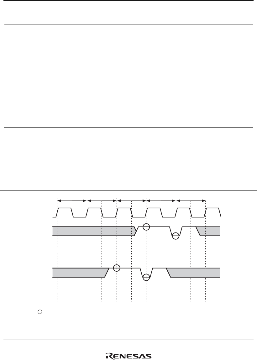
11. Local Bus State Controller (LBSC)
Rev.1.00 Jan. 10, 2008 Page 370 of 1658
REJ09B0261-0100
Bit Bit Name
Initial
Value R/W Description
6 to 0 ASYNC[6:0] All 0 R/W Asynchronous Input
These bits enable asynchronous inputs of the
corresponding pins.
0: CLKOUT-synchronous inputs to the corresponding
pins
1: CLKOUT-asynchronous inputs to the corresponding
pins
ASYNC[6]: DREQ3
ASYNC[5]: DREQ2
ASYNC[4]: DREQ1
ASYNC[3]: DREQ0
ASYNC[2]: IOIS16
ASYNC[1]: BREQ
ASYNC[0]: RDY
When asynchronous input is set (ASYNCn = 1), the sampling timing is one cycle before the
synchronous input setting (see figure 11.4).
The timing shown in this section, other sections and section 32 Electrical Characteristics is that
with synchronous input setting (ASYNCn = 0). Note that the setup/hold time must be satisfied
when synchronous input is set.
T1
CLKOUT
Tw TweTw T2
RDY
(BCR.ASYNC0 = 0)
RDY
(BCR.ASYNC0 = 1)
: Sampling Timing
Figure 11.4 RDY Sampling Timings with ASYNCn Settings
(Two Wait Cycles Inserted by CSnWCR.)

11. Local Bus State Controller (LBSC)
Rev.1.00 Jan. 10, 2008 Page 371 of 1658
REJ09B0261-0100
11.4.3 CSn Bus Control Register (CSnBCR)
CSnBCR are 32-bit readable/writable registers that specify the bus width for area n (n = 0 to 6),
idle mode between cycles, burst ROM setting and memory types.
Some types of memory continue to drive the data bus immediately after the read signal is turned
off. Therefore, data buses may collide with each other when different memory areas are accessed
consecutively or memory writing is performed immediately after it is read. This LSI automatically
inserts idle cycles as specified with CSnBCR when the data buses may collide. In the idle cycles,
CSn, RD, WEn, CE2A, CE2B, BS and R/W are set to high, and the data bus is not driven.
CSnBCR is initialized to H'7777 77F0 at a power-on reset, but is not initialized by a manual reset.
161718192021222324252627282931 30
1110111011101101
IWRRD⎯IWRWS⎯IWRWD⎯IWW⎯
R/WR/WR/WRR/WR/WR/WRR/WR/WR/WRR/WR/WR R/W
BIt:
Initial value:
R/W:
01234567891011121315 14
0000111111101101
TYPEMPX*BW
RDSPLSZ*BSTIWRRS⎯
R/WR/WR/WR/W*R/WR/WR/WR/WR/W*R/W*R/WR/WR/WR/WR
Note: * Bits SZ and MPX in CS0BCR are read-only.
R/W
BIt:
Initial value:
R/W:
Bit Bit Name
Initial
Value R/W Description
31 ⎯ 0 R Reserved
This bit is always read as 0. The write value should
always be 0.

11. Local Bus State Controller (LBSC)
Rev.1.00 Jan. 10, 2008 Page 372 of 1658
REJ09B0261-0100
Bit Bit Name
Initial
Value R/W Description
30 to 28 IWW 111 R/W Idle Cycles between Write-Read/Write-Write
These bits specify the number of idle cycles to be
inserted after the access of the memory connected to
the space. The target cycles are write-read and write-
write cycles. For details, see section 11.5.8, Wait
Cycles between Access Cycles.
000: No idle cycle inserted
001: 1 idle cycle inserted
010: 2 idle cycles inserted
011: 3 idle cycles inserted
100: 4 idle cycles inserted
101: 5 idle cycles inserted
110: 6 idle cycles inserted
111: 7 idle cycles inserted
27 ⎯ 0 R Reserved
This bit is always read as 0. The write value should
always be 0.
26 to 24 IWRWD 111 R/W Idle Cycles between Read-Write in Different Spaces
These bits specify the number of idle cycles to be
inserted after the access of the memory connected to
the space. The target cycles are read-write cycles in
which consecutive accesses are performed to different
spaces. For details, see section 11.5.8, Wait Cycles
between Access Cycles.
000: No idle cycle inserted
001: 1 idle cycle inserted
010: 2 idle cycles inserted
011: 3 idle cycles inserted
100: 4 idle cycles inserted
101: 5 idle cycles inserted
110: 6 idle cycles inserted
111: 7 idle cycles inserted

11. Local Bus State Controller (LBSC)
Rev.1.00 Jan. 10, 2008 Page 373 of 1658
REJ09B0261-0100
Bit Bit Name
Initial
Value R/W Description
23 ⎯ 0 R Reserved
This bit is always read as 0. The write value should
always be 0.
22 to 20 IWRWS 111 R/W Idle Cycles between Read-Write in Same Space
These bits specify the number of idle cycles to be
inserted after the access to the memory connected to
the space. The target cycles are read-write cycles in
which consecutive accesses are performed to the same
space. For details, see section 11.5.8, Wait Cycles
between Access Cycles.
000: No idle cycle inserted
001: 1 idle cycle inserted
010: 2 idle cycles inserted
011: 3 idle cycles inserted
100: 4 idle cycles inserted
101: 5 idle cycles inserted
110: 6 idle cycles inserted
111: 7 idle cycles inserted
19 ⎯ 0 R Reserved
This bit is always read as 0. The write value should
always be 0.
18 to 16 IWRRD 111 R/W Idle Cycles between Read-Read in Different Spaces
These bits specify the number of idle cycles to be
inserted after the memory connected to the space is
accessed. The target cycles are read-read cycles in
which consecutive accesses are performed to different
spaces. For details, see section 11.5.8, Wait Cycles
between Access Cycles.
000: No idle cycle inserted
001: 1 idle cycle inserted
010: 2 idle cycles inserted
011: 3 idle cycles inserted
100: 4 idle cycles inserted
101: 5 idle cycles inserted
110: 6 idle cycles inserted
111: 7 idle cycles inserted

11. Local Bus State Controller (LBSC)
Rev.1.00 Jan. 10, 2008 Page 374 of 1658
REJ09B0261-0100
Bit Bit Name
Initial
Value R/W Description
15 ⎯ 0 R Reserved
This bit is always read as 0. The write value should
always be 0.
14 to 12 IWRRS 111 R/W Idle Cycles between Read-Read in Same Space
These bits specify the number of idle cycles to be
inserted after the memory connected to the space is
accessed. The target cycles are read-read cycles in
which consecutive accesses are performed to the same
space. For details, see section 11.5.8, Wait Cycles
between Access Cycles.
000: No idle cycle inserted
001: 1 idle cycle inserted
010: 2 idle cycles inserted
011: 3 idle cycles inserted
100: 4 idle cycles inserted
101: 5 idle cycles inserted
110: 6 idle cycles inserted
111: 7 idle cycles inserted
11, 10 BST 01 R/W Burst Number
These bits specify the number of bursts when the burst
ROM interface is used. The MPX interface is not
affected.
00: 4 consecutive accesses (Can be used with 8-, 16-,
or 32-bit bus width)
01: 8 consecutive accesses (Can be used with 8-, 16-,
or 32-bit bus width)
10: 16 consecutive accesses (Can be used with 8-, or
16-bit bus width)
11: 32 consecutive accesses (Can be used with 8-bit
bus width)

11. Local Bus State Controller (LBSC)
Rev.1.00 Jan. 10, 2008 Page 375 of 1658
REJ09B0261-0100
Bit Bit Name
Initial
Value R/W Description
9, 8 SZ 11 R/W* Bus Width
In CS0BCR, the external pins (MODE5 and MODE6) to
specify the bus size are sampled at a power-on reset.
When using the MPX interface, set these bits to 00 or
11. When using the byte control SRAM interface, set
these bits to 00, 10 or 11.
00: 64 bits (can be specified when the MODE 12 and
MODE 11 pins are set to 1 and 0 respectively.)
01: 8 bits
10: 16 bits
11: 32 bits
Note: * The SZ bits in CS0BCR are read-only. When
area 0 is set to the MPX interface by the
MODE7 pin, the SZ bits in CS0BCR should be
set to 00 or 11.
7 RDSPL 1 R/W RD Hold Cycle
Specifies the number of cycles to be inserted in the
hold time for the read data sample timing of RD. When
setting this bit to 1, specify the number of RD negation-
CSn negation delay cycles set by the RDH bit in
CSnWCR as 1 or more. Also the RD negation-CSn
negation delay cycle is reduced 1 cycle when this bit is
set to 1 (valid only when the SRAM interface, burst
ROM interface, or byte control SRAM interface is
selected).
0: No hold cycle inserted
1: 1 hold cycle inserted

11. Local Bus State Controller (LBSC)
Rev.1.00 Jan. 10, 2008 Page 376 of 1658
REJ09B0261-0100
Bit Bit Name
Initial
Value R/W Description
6 to 4 BW 111 R/W Burst Pitch
When the burst ROM interface is used, these bits
specify the number of wait cycles to be inserted after
the second data access in a burst transfer.
000: No idle cycle inserted, RDY pin disabled
001: 1 idle cycle inserted, RDY pin enabled
010: 2 idle cycles inserted, RDY pin enabled
011: 3 idle cycles inserted, RDY pin enabled
100: 4 idle cycles inserted, RDY pin enabled
101: 5 idle cycles inserted, RDY pin enabled
110: 6 idle cycles inserted, RDY pin enabled
111: 7 idle cycles inserted, RDY pin enabled
3 MPX 0 R/W* MPX Interface Setting
Selects the type of the MPX interface
0: Memory type set by bits TYPE2 to TYPE0 is selected
1: MPX interface is selected
Note: * The MPX bit in CS0BCR is read-only.
2 to 0 TYPE 000 R/W Memory Type Setting
These bits specify the type of memory connected to the
space.
000: SRAM (Initial value)
001: SRAM with byte-control*1
010: Burst ROM (burst at read/SRAM at write)
011: Reserved (Setting prohibited)
100: PCMCIA *2
101: Reserved (Setting prohibited)
110: Reserved (Setting prohibited)
111: Reserved (Setting prohibited)
Notes: 1. Setting enabled only in CS1BCR and
CS4BCR
2. Setting enabled only in CS5BCR and
CS6BCR

11. Local Bus State Controller (LBSC)
Rev.1.00 Jan. 10, 2008 Page 377 of 1658
REJ09B0261-0100
11.4.4 CSn Wait Control Register (CSnWCR)
CSnWCR (n = 0 to 6) are 32-bit readable/writable registers that specify the number of wait cycles
to be inserted for areas 0 to 6, the number of wait cycles to be inserted preceding the first data in
burst memory access, the address setup time, which is the time from the point at which the output
of address for access is started until assertion of the read/write strobe signal, and the number of
cycles to be inserted as the data hold time from negation of the write strobe signal.
CSnWCR is initialized to H'7777 770F by a power-on reset, but it is not initialized by a manual
reset.
161718192021222324252627282931 30
1110111011101101
RDH⎯RDS⎯ADH⎯ADS⎯
R/WR/WR/WRR/WR/WR/WRR/WR/WR/WRR/WR/WR R/W
BIt:
Initial value:
R/W:
⎯⎯
01234567891011121315 14
1111000011101101
IW[3:0]BSHWTHWTS⎯
R/WR/WR/WR/WR/WR/WR/WRR/WR/WR/WR/WR/WR/WR R/W
BIt:
Initial value:
R/W:
Bit Bit Name
Initial
Value R/W Description
31 ⎯ 0 R Reserved
This bit is always read as 0. The write value should
always be 0.
30 to 28 ADS 111 R/W Address Setup Cycle
These bits specify the number of cycles to be inserted
as the address setup time with respect to CSn
assertion. (Only valid when the SRAM interface, byte
control SRAM interface, or burst ROM interface is
selected.)
000: No cycle inserted
001: 1 cycle inserted
010: 2 cycles inserted
011: 3 cycles inserted
100: 4 cycles inserted
101: 5 cycles inserted
110: 6 cycles inserted
111: 7 cycles inserted

11. Local Bus State Controller (LBSC)
Rev.1.00 Jan. 10, 2008 Page 378 of 1658
REJ09B0261-0100
Bit Bit Name
Initial
Value R/W Description
27 ⎯ 0 R Reserved
This bit is always read as 0. The write value should
always be 0.
26 to 24 ADH 111 R/W Address Hold Cycle
These bits specify the number of cycles to be inserted
as the address hold time with respect to CSn negation.
(Only valid when the SRAM interface, byte control
SRAM interface, or burst ROM interface is selected.)
000: No cycle inserted
001: 1 cycle inserted
010: 2 cycles inserted
011: 3 cycles inserted
100: 4 cycles inserted
101: 5 cycles inserted
110: 6 cycles inserted
111: 7 cycles inserted
23 ⎯ 0 R Reserved
This bit is always read as 0. The write value should
always be 0.
22 to 20 RDS 111 R/W RD Setup Cycle (CSn Assertion–RD Assertion Delay
Cycle)
These bits specify the number of cycles to be inserted
as the time from CSn assertion to RD assertion. (Only
valid only when the SRAM interface, byte control SRAM
interface, or burst ROM interface is selected.)
000: No cycle inserted (1 cycle delayed)
001: 1 cycle inserted (2 cycles delayed)
010: 2 cycles inserted (3 cycles delayed)
011: 3 cycles inserted (4 cycles delayed)
100: 4 cycles inserted (5 cycles delayed)
101: 5 cycles inserted (6 cycles delayed)
110: 6 cycles inserted (7 cycles delayed)
111: 7 cycles inserted (8 cycles delayed)

11. Local Bus State Controller (LBSC)
Rev.1.00 Jan. 10, 2008 Page 379 of 1658
REJ09B0261-0100
Bit Bit Name
Initial
Value R/W Description
19 ⎯ 0 R Reserved
This bit is always read as 0. The write value should
always be 0.
18 to 16 RDH 111 R/W RD Hold Cycle (RD Negation–CSn Negation Delay
Cycle)
These bits specify the number of cycles to be inserted
as the time from RD negation to CSn negation. (Only
valid when the SRAM interface, byte control SRAM
interface, or burst ROM interface is selected.)
000: No cycle inserted (0 cycle delayed)
001: 1 cycle inserted (1 cycle delayed)
010: 2 cycles inserted (2 cycles delayed)
011: 3 cycles inserted (3 cycles delayed)
100: 4 cycles inserted (4 cycles delayed)
101: 5 cycles inserted (5 cycles delayed)
110: 6 cycles inserted (6 cycles delayed)
111: 7 cycles inserted (7 cycles delayed)
15 ⎯ 0 R Reserved
This bit is always read as 0. The write value should
always be 0.
14 to 12 WTS 111 R/W WE Setup Cycle (CSn Assertion–WE Assertion Delay
Cycle)
These bits specify the number of cycles to be inserted
as the time from CSn assertion to WE assertion. (Only
valid when the SRAM interface, byte control SRAM
interface, or burst ROM interface is selected.)
000: No cycle inserted (0.5 cycle delayed)
001: 1 cycle inserted (1.5 cycles delayed)
010: 2 cycles inserted (2.5 cycles delayed)
011: 3 cycles inserted (3.5 cycles delayed)
100: 4 cycles inserted (4.5 cycles delayed)
101: 5 cycles inserted (5.5 cycles delayed)
110: 6 cycles inserted (6.5 cycles delayed)
111: 7 cycles inserted (7.5 cycles delayed)

11. Local Bus State Controller (LBSC)
Rev.1.00 Jan. 10, 2008 Page 380 of 1658
REJ09B0261-0100
Bit Bit Name
Initial
Value R/W Description
11 ⎯ 0 R Reserved
This bit is always read as 0. The write value should
always be 0.
10 to 8 WTH 111 R/W WE Hold Cycle (WE Negation–CSn Negation Delay
Cycle)
These bits specify the number of cycles to be inserted
as the time from WE negation to CSn negation. (Only
valid when the SRAM interface, byte control SRAM
interface, or burst ROM interface is selected.)
000: No cycle inserted (0.5 cycle delayed)
001: 1 cycle inserted (1.5 cycles delayed)
010: 2 cycles inserted (2.5 cycles delayed)
011: 3 cycles inserted (3.5 cycles delayed)
100: 4 cycles inserted (4.5 cycles delayed)
101: 5 cycles inserted (5.5 cycles delayed)
110: 6 cycles inserted (6.5 cycles delayed)
111: 7 cycles inserted (7.5 cycles delayed)
7 ⎯ 0 R Reserved
This bit is always read as 0. The write value should
always be 0.
6 to 4 BSH 000 R/W BS Hold Cycle
These bits specify the number of cycles to extend BS
assertion. The extension of the assertion is valid when
the RDS bits in CSnWCR are not set to 000 in reading
and when the WTS bits in CSnWCR are not set to 000
in writing. The total access cycle count is not changed
by setting these bits.
000: BS assertion is 1 cycle
001: BS assertion is 2 cycles
010: Setting prohibited
011: Setting prohibited
100: Setting prohibited
101: Setting prohibited
110: Setting prohibited
111: Setting prohibited

11. Local Bus State Controller (LBSC)
Rev.1.00 Jan. 10, 2008 Page 381 of 1658
REJ09B0261-0100
Bit Bit Name
Initial
Value R/W Description
3 to 0 IW[3:0] 1111 R/W Insert Wait Cycle
These bits specify the number of wait cycles to be
inserted. The wait cycles are as follows when the
SRAM interface, byte control SRAM interface, burst
ROM interface (first data cycle only), or PCMCIA
interface is selected. Insertion of external wait cycles by
the RDY pin is not possible when "no cycle inserted" is
selected.
0000: No cycle inserted 1000: 8 cycles inserted
0001: 1 cycle inserted 1001: 9 cycles inserted
0010: 2 cycles inserted 1010: 11 cycles inserted
0011: 3 cycles inserted 1011: 13 cycles inserted
0100: 4 cycles inserted 1100: 15 cycles inserted
0101: 5 cycles inserted 1101: 17 cycles inserted
0110: 6 cycles inserted 1110: 21 cycles inserted
0111: 7 cycles inserted 1111: 25 cycles inserted
When MPX interface is selected, the wait cycles are
inserted as follows according to the IW[2:0] setting. The
IW[3] setting is invalid. The external wait cycles can be
inserted by the RDY pin in any settings.
IW[2] specifies wait cycle insertion for the second and
subsequent data:
0: No cycle inserted
1: 1 cycle inserted
IW[1:0] specifies wait cycle insertion for the first data:
00: 1 cycle inserted in reading and no cycle inserted in
writing
01: 1 cycle inserted in reading and 1 cycle inserted in
writing
10: 2 cycles inserted in reading and 2 cycles inserted in
writing
11: 3 cycles inserted in reading and 3 cycles inserted in
writing

11. Local Bus State Controller (LBSC)
Rev.1.00 Jan. 10, 2008 Page 382 of 1658
REJ09B0261-0100
11.4.5 CSn PCMCIA Control Register (CSnPCR)
CSnPCR is a 32-bit readable/writable register that specifies the timing for the PCMCIA interface
connected to area n (CSnPCR, n = 5 or 6), the space property, and the assert/negate timing for the
OE and WE signals. Also, areas 5 and 6 in CSnPCR can be set for the first half and second half
individually. The first half of area 5 is allocated from H'1400 0000 to H'15FF FFFF, and the
second half of area 5 is allocated from H'1600 0000 to H'17FF FFFF. The first half of area 6 is
allocated from H'1800 0000 to H'19FF FFFF, and the second half of area 6 is allocated from
H'1A00 0000 to H'1BFF FFFF (these addresses are the local bus address). The pulse widths of OE
and WE assertion for the first half of area 5 and 6 are set by the IW bits in CSnWCR.
CSnPCR is initialized to H'7700 0000 by a power-on reset, but it is not initialized by a manual
reset.
161718192021222324252627282931 30
0000000011101101
PCIWPCWA PCWBSAB⎯SAA⎯
R/WR/WR/WR/WR/WR/WR/WR/WR/WR/WR/WRR/WR/WR R/W
BIt:
Initial value:
R/W:
⎯⎯⎯
01234567891011121315 14
0000000000000000
TEHBTEHATEDBTEDA⎯
R/WR/WR/WRR/WR/WR/WRR/WR/WR/WRR/WR/WR R/W
BIt:
Initial value:
R/W:
Bit Bit Name
Initial
Value R/W Description
31 ⎯ 0 R Reserved
This bit is always read as 0. The write value should
always be 0.
30 to 28 SAA 111 R/W Space Property A
These bits specify the space property of PCMCIA
connected to the first half of the area.
000: ATA complement mode
001: Dynamic I/O bus sizing
010: 8-bit I/O space
011: 16-bit I/O space
100: 8-bit common memory
101: 16-bit common memory
110: 8-bit attribute memory
111: 16-bit attribute memory

11. Local Bus State Controller (LBSC)
Rev.1.00 Jan. 10, 2008 Page 383 of 1658
REJ09B0261-0100
Bit Bit Name
Initial
Value R/W Description
27 ⎯ 0 R Reserved
This bit is always read as 0. The write value should
always be 0.
26 to 24 SAB 111 R/W Space Property B
These bits specify the space property of PCMCIA
connected to the second half of the area.
000: ATA complement mode
001: Dynamic I/O bus sizing
010: 8-bit I/O space
011: 16-bit I/O space
100: 8-bit common memory
101: 16-bit common memory
110: 8-bit attribute memory
111: 16-bit attribute memory
23, 22 PCWA 00 R/W PCMCIA Wait A
These bits specify the number of wait cycles for low-
speed PCMCIA, which is added to the number set by
the IW bits in CSnWCR.
The bit settings are selected when the access area of
PCMCIA interface is the first half.
00: No wait cycle inserted
01: 15 wait cycles inserted
10: 30 wait cycles inserted
11: 50 wait cycles inserted
21, 20 PCWB 00 R/W PCMCIA Wait B
These bits specify the number of wait cycles for low-
speed PCMCIA, which is added to the number set by
the PCIW bits.
The bit settings are selected when the access area of
PCMCIA interface is the second half.
00: No wait cycle inserted
01: 15 wait cycles inserted
10: 30 wait cycles inserted
11: 50 wait cycles inserted

11. Local Bus State Controller (LBSC)
Rev.1.00 Jan. 10, 2008 Page 384 of 1658
REJ09B0261-0100
Bit Bit Name
Initial
Value R/W Description
19 to 16 PCIW 0000 R/W PCMCIA Insert Wait Cycle B
These bits specify the number of wait cycles to be
inserted. The bit settings are selected when the access
area of PCMCIA interface is the second half. When the
access area of PCMCIA interface is the first half, the
number of wait cycles set by the IW bit in CSnWCR is
selected.
0000: No cycle inserted
0001: 1 cycle inserted
0010: 2 cycles inserted
0011: 3 cycles inserted
0100: 4 cycles inserted
0101: 5 cycles inserted
0110: 6 cycles inserted
0111: 7 cycles inserted
1000: 8 cycles inserted
1001: 9 cycles inserted
1010: 11 cycles inserted
1011: 13 cycles inserted
1100: 15 cycles inserted
1101: 17 cycles inserted
1110: 21 cycles inserted
1111: 25 cycles inserted
15 ⎯ 0 R Reserved
This bit is always read as 0. The write value should
always be 0.

11. Local Bus State Controller (LBSC)
Rev.1.00 Jan. 10, 2008 Page 385 of 1658
REJ09B0261-0100
Bit Bit Name
Initial
Value R/W Description
14 to 12 TEDA 000 R/W OE/WE Assert Delay A
These bits set the delay time from address output to
OE/WE assertion when the first half area is accessed
with the connected PCMCIA interface.
000: No wait cycle inserted
001: 1 wait cycle inserted
010: 2 wait cycles inserted
011: 3 wait cycles inserted
100: 6 wait cycles inserted
101: 9 wait cycles inserted
110: 12 wait cycles inserted
111: 15 wait cycles inserted
11 ⎯ 0 R Reserved
This bit is always read as 0. The write value should
always be 0.
10 to 8 TEDB 000 R/W OE/WE Assert Delay B
These bits set the delay time from address output to
OE/WE assertion when the second half area is
accessed with the connected PCMCIA interface.
000: No wait cycle inserted
001: 1 wait cycle inserted
010: 2 wait cycles inserted
011: 3 wait cycles inserted
100: 6 wait cycles inserted
101: 9 wait cycles inserted
110: 12 wait cycles inserted
111: 15 wait cycles inserted
7 ⎯ 0 R Reserved
This bit is always read as 0. The write value should
always be 0.

11. Local Bus State Controller (LBSC)
Rev.1.00 Jan. 10, 2008 Page 386 of 1658
REJ09B0261-0100
Bit Bit Name
Initial
Value R/W Description
6 to 4 TEHA 000 R/W OE/WE Negation-Address Delay A
These bits set the delay time from OE/WE negation to
address hold when the first half area is accessed with
the connected PCMCIA interface.
000: No wait cycle inserted
001: 1 wait cycle inserted
010: 2 wait cycles inserted
011: 3 wait cycles inserted
100: 6 wait cycles inserted
101: 9 wait cycles inserted
110: 12 wait cycles inserted
111: 15 wait cycles inserted
3 ⎯ 0 R Reserved
This bit is always read as 0. The write value should
always be 0.
2 to 0 TEHB 000 R/W OE/WE Negation-Address Delay B
These bits set the delay time from OE/WE negation to
address hold when the second half area is accessed
with the connected PCMCIA interface.
000: No wait cycle inserted
001: 1 wait cycle inserted
010: 2 wait cycles inserted
011: 3 wait cycles inserted
100: 6 wait cycles inserted
101: 9 wait cycles inserted
110: 12 wait cycles inserted
111: 15 wait cycles inserted

11. Local Bus State Controller (LBSC)
Rev.1.00 Jan. 10, 2008 Page 387 of 1658
REJ09B0261-0100
11.5 Operation
11.5.1 Endian/Access Size and Data Alignment
This LSI supports both big and little endian modes. In big endian mode, the most significant byte
(MSByte) in a string of byte data is stored at address 0, and in little endian mode, the least
significant byte (LSByte) in a string of byte data is stored at address 0. The mode is specified by
the external pin (MODE8 pin) at a power-on reset by the PRESET pin. At a power-on reset by the
PRESET pin, big endian mode is specified when the MODE8 pin is low, and little endian mode is
specified when the MODE8 pin is high.
The data bus width can be selected from 8, 16 and 32 bits for the normal memory interface. For
the PCMCIA interface, a data bus width of 8 or 16 bits can be selected. Data is aligned according
to the data bus width and endian mode of each device. Therefore, when the data bus width is
smaller than the access size, multiple bus cycles are automatically generated to reach the access
size. In this case, access is performed by incrementing the addresses corresponding to the bus
width. For example, when a longword access is performed in the area with an 8-bit width with the
SRAM interface, each address is incremented by one, and accesses are performed four times. In
the 32-byte transfer, a total of 32-byte data is continuously transferred according to the specified
bus width. The first access is performed on the data for which there was an access request, and the
remaining accesses are performed on the subsequent data up to the nearest 32-byte boundary in a
wraparound manner. The bus is not released during these transfers. This LSI automatically aligns
data and changes the data length between interfaces.
In an 8- or 16-byte transfer, the LBSC executes the 4-byte accesses twice and four times
respectively.
Tables 11.6 to 11.15 show the relationship between the device data width, endian mode and access
size.
Data structure
Data 7 to 0
Data 15 to 8 Data 7 to 0
Data 31 to 24 Data 23 to 16 Data 15 to 8 Data 7 to 0
MSB LSB
MSB LSB LSB
MSB LSB
Byte
Word
Longword

11. Local Bus State Controller (LBSC)
Rev.1.00 Jan. 10, 2008 Page 388 of 1658
REJ09B0261-0100
Table 11.6 64-Bit External Device/Big Endian Access and Data Alignment (1)
Operation Data Bus
Access
Size Address No.
D63 to
D56
D55 to
D48
D47 to
D40
D39 to
D32
D31 to
D24
D23 to
D16 D15 to D8 D7 to D0
8n 1 Data 7 to 0 ⎯ ⎯ ⎯ ⎯ ⎯ ⎯ ⎯
8n + 1 1 ⎯ Data 7 to 0 ⎯ ⎯ ⎯ ⎯ ⎯ ⎯
8n + 2 1 ⎯ ⎯ Data 7 to 0 ⎯ ⎯ ⎯ ⎯ ⎯
8n + 3 1 ⎯ ⎯ ⎯ Data 7 to 0 ⎯ ⎯ ⎯ ⎯
8n + 4 1 ⎯ ⎯ ⎯ ⎯ Data 7 to 0 ⎯ ⎯ ⎯
8n + 5 1 ⎯ ⎯ ⎯ ⎯ ⎯ Data 7 to 0 ⎯ ⎯
8n + 6 1 ⎯ ⎯ ⎯ ⎯ ⎯ ⎯ Data 7 to 0 ⎯
Byte
8n + 7 1 ⎯ ⎯ ⎯ ⎯ ⎯ ⎯ ⎯ Data 7 to 0
8n 1 Data
15 to 8
Data
7 to 0
⎯ ⎯ ⎯ ⎯ ⎯ ⎯
8n + 2 1 ⎯ ⎯ Data
15 to 8
Data
7 to 0
⎯ ⎯ ⎯ ⎯
8n + 4 1 ⎯ ⎯ ⎯ ⎯ Data
15 to 8
Data
7 to 0
⎯ ⎯
Word
8n + 6 1 ⎯ ⎯ ⎯ ⎯ ⎯ ⎯ Data
15 to 8
Data
7 to 0
8n 1 Data
31 to 24
Data
23 to 16
Data
15 to 8
Data
7 to 0
⎯ ⎯ ⎯ ⎯ Longword
8n + 4 1 ⎯ ⎯ ⎯ ⎯ Data
31 to 24
Data
23 to 16
Data
15 to 8
Data
7 to 0
32 Bytes* 8n 1 Data
63 to 56
Data
55 to 48
Data
47 to 40
Data
39 to 32
Data
31 to 24
Data
23 to 16
Data
15 to 8
Data
7 to 0
8n + 8 2 Data 127
to 120
Data 119
to 112
Data 111
to 104
Data 103
to 96
Data 95 to
88
Data 87 to
80
Data 79 to
72
Data 71 to
64
8n + 16 3 Data 191
to 184
Data 183
to 176
Data 175
to 168
Data 167
to 160
Data 159
to 152
Data 151
to 144
Data 143
to 136
Data 135
to 128
8n + 24 4 Data 255
to 248
Data 247
to 240
Data 239
to 232
Data 231
to 224
Data 223
to 216
Data 215
to 208
Data 207
to 200
Data 199
to 192
Note: * This table shows an example when the access start address is on the 32-byte
boundary. When the start address is not on the 32-byte boundary, accesses are
performed up to immediately before the 32-byte boundary and the address is wrapped
around to the previous 32-byte boundary.

11. Local Bus State Controller (LBSC)
Rev.1.00 Jan. 10, 2008 Page 389 of 1658
REJ09B0261-0100
Table 11.7 64-Bit External Device/Big Endian Access and Data Alignment (2)
Operation Strobe Signal
Access
Size Address No. WE7 WE6 WE5 WE4 WE3 WE2 WE1 WE0
8n 1 Asserted ⎯ ⎯ ⎯ ⎯ ⎯ ⎯ ⎯
8n + 1 1 ⎯ Asserted ⎯ ⎯ ⎯ ⎯ ⎯ ⎯
8n + 2 1 ⎯ ⎯ Asserted ⎯ ⎯ ⎯ ⎯ ⎯
8n + 3 1 ⎯ ⎯ ⎯ Asserted ⎯ ⎯ ⎯ ⎯
8n + 4 1 ⎯ ⎯ ⎯ ⎯ Asserted ⎯ ⎯ ⎯
8n + 5 1 ⎯ ⎯ ⎯ ⎯ ⎯ Asserted ⎯ ⎯
8n + 6 1 ⎯ ⎯ ⎯ ⎯ ⎯ ⎯ Asserted ⎯
Byte
8n + 7 1 ⎯ ⎯ ⎯ ⎯ ⎯ ⎯ ⎯ Asserted
8n 1 Asserted Asserted ⎯ ⎯ ⎯ ⎯ ⎯ ⎯
8n + 2 1 ⎯ ⎯ Asserted Asserted ⎯ ⎯ ⎯ ⎯
8n + 4 1 ⎯ ⎯ ⎯ ⎯ Asserted Asserted ⎯ ⎯
Word
8n + 6 1 ⎯ ⎯ ⎯ ⎯ ⎯ ⎯ Asserted Asserted
8n 1 Asserted Asserted Asserted Asserted ⎯ ⎯ ⎯ ⎯ Longword
8n + 4 1 ⎯ ⎯ ⎯ ⎯ Asserted Asserted Asserted Asserted
32 Bytes* 8n 1 Asserted Asserted Asserted Asserted Asserted Asserted Asserted Asserted
8n + 8 2 Asserted Asserted Asserted Asserted Asserted Asserted Asserted Asserted
8n + 16 3 Asserted Asserted Asserted Asserted Asserted Asserted Asserted Asserted
8n + 24 4 Asserted Asserted Asserted Asserted Asserted Asserted Asserted Asserted
Note: * This table shows an example when the access start address is on the 32-byte
boundary. When the start address is not on the 32-byte boundary, accesses are
performed up to immediately before the 32-byte boundary and the address is wrapped
around to the previous 32-byte boundary.

11. Local Bus State Controller (LBSC)
Rev.1.00 Jan. 10, 2008 Page 390 of 1658
REJ09B0261-0100
Table 11.8 32-Bit External Device/Big-Endian Access and Data Alignment
Operation Data Bus Strobe Signals
Access
Size Address No.
D31 to
D24
D23 to
D16
D15 to
D8
D7 to
D0 WE3 WE2 WE1 WE0
4n 1 Data
7 to 0
⎯ ⎯ ⎯ Asserted
4n + 1 1 ⎯ Data
7 to 0
⎯ ⎯ Asserted
4n + 2 1 ⎯ ⎯ Data
7 to 0
⎯ Asserted
Byte
4n + 3 1 ⎯ ⎯ ⎯ Data
7 to 0
Asserted
4n 1 Data
15 to 8
Data
7 to 0
⎯ ⎯ Asserted Asserted Word
4n + 2 1 ⎯ ⎯ Data
15 to 8
Data
7 to 0
Asserted Asserted
Longword 4n 1 Data
31 to 24
Data
23 to 16
Data
15 to 8
Data
7 to 0
Asserted Asserted Asserted Asserted
32 Bytes* 8n 1 Data
31 to 24
Data
23 to 16
Data
15 to 8
Data
7 to 0
Asserted Asserted Asserted Asserted
8n + 4 2 Data
63 to 56
Data
55 to 48
Data
47 to 40
Data
39 to 32
Asserted Asserted Asserted Asserted
8n + 8 3 Data
95 to 88
Data
87 to 80
Data
79 to 72
Data
71 to 64
Asserted Asserted Asserted Asserted
… … … … … … … … … …
8n + 28 8 Data
255 to
248
Data
247 to
240
Data
239 to
232
Data
231 to
224
Asserted Asserted Asserted Asserted
Note: * This table shows an example when the access start address is on the 32-byte
boundary. When the start address is not on the 32-byte boundary, accesses are
performed up to immediately before the 32-byte boundary and the address is wrapped
around to the previous 32-byte boundary.

11. Local Bus State Controller (LBSC)
Rev.1.00 Jan. 10, 2008 Page 391 of 1658
REJ09B0261-0100
Table 11.9 16-Bit External Device/Big-Endian Access and Data Alignment
Operation Data Bus Strobe Signals
Access
Size Address No.
D31 to
D24
D23 to
D16
D15 to
D8
D7 to
D0 WE3 WE2 WE1 WE0
2n 1 ⎯ ⎯ Data
7 to 0
⎯ Asserted Byte
2n + 1 1 ⎯ ⎯ ⎯ Data
7 to 0
Asserted
Word 2n 1 ⎯ ⎯ Data
15 to 8
Data
7 to 0
Asserted Asserted
4n 1 ⎯ ⎯ Data
31 to 24
Data
23 to 16
Asserted AssertedLongword
4n + 2 2 ⎯ ⎯ Data
15 to 8
Data
7 to 0
Asserted Asserted
32 Bytes 8n 1 ⎯ ⎯ Data
15 to 8
Data
7 to 0
Asserted Asserted
8n + 2 2 ⎯ ⎯ Data
31 to 24
Data
23 to 16
Asserted Asserted
8n + 4 3 ⎯ ⎯ Data
47 to 40
Data
39 to 32
Asserted Asserted
… … … … … … … … … …
8n + 30 16 ⎯ ⎯ Data
255 to
248
Data
247 to
240
Asserted Asserted
Note: * This table shows an example when the access start address is on the 32-byte
boundary. When the start address is not on the 32-byte boundary, accesses are
performed up to immediately before the 32-byte boundary and the address is wrapped
around to the previous 32-byte boundary.

11. Local Bus State Controller (LBSC)
Rev.1.00 Jan. 10, 2008 Page 392 of 1658
REJ09B0261-0100
Table 11.10 8-Bit External Device/Big-Endian Access and Data Alignment
Operation Data Bus Strobe Signals
Access
Size Address No.
D31 to
D24
D23 to
D16
D15 to
D8
D7 to
D0 WE3 WE2 WE1 WE0
Byte n 1 ⎯ ⎯ ⎯ Data
7 to 0
Asserted
2n 1 ⎯ ⎯ ⎯ Data
15 to 8
AssertedWord
2n + 1 2 ⎯ ⎯ ⎯ Data
7 to 0
Asserted
4n 1 ⎯ ⎯ Data
31 to 24
Asserted
4n + 1 2 ⎯ ⎯ ⎯ Data
23 to 16
Asserted
4n + 2 3 ⎯ ⎯ ⎯ Data
15 to 8
Asserted
Longword
4n + 3 4 ⎯ ⎯ ⎯ Data
7 to 0
Asserted
32 Bytes* 8n 1 ⎯ ⎯ ⎯ Data 7
to 0
Asserted
8n + 1 2 ⎯ ⎯ ⎯ Data 15
to 8
Asserted
8n + 2 3 ⎯ ⎯ ⎯ Data 23
to 16
Asserted
… … … … … … … … … …
8n + 31 32 ⎯ ⎯ ⎯ Data
255 to
248
Asserted
Note: * This table shows an example when the access start address is on the 32-byte
boundary. When the start address is not on the 32-byte boundary, accesses are
performed up to immediately before the 32-byte boundary and the address is wrapped
around to the previous 32-byte boundary.

11. Local Bus State Controller (LBSC)
Rev.1.00 Jan. 10, 2008 Page 393 of 1658
REJ09B0261-0100
Table 11.11 64-Bit External Device/Little Endian Access and Data Alignment (1)
Operation Data Bus
Access
Size Address No.
D63 to
D56
D55 to
D48
D47 to
D40
D39 to
D32
D31 to
D24
D23 to
D16 D15 to D8 D7 to D0
8n 1 ⎯ ⎯ ⎯ ⎯ ⎯ ⎯ ⎯ Data 7 to 0
8n + 1 1 ⎯ ⎯ ⎯ ⎯ ⎯ ⎯ Data 7 to 0 ⎯
8n + 2 1 ⎯ ⎯ ⎯ ⎯ ⎯ Data 7 to 0 ⎯ ⎯
8n + 3 1 ⎯ ⎯ ⎯ ⎯ Data 7 to 0 ⎯ ⎯ ⎯
8n + 4 1 ⎯ ⎯ ⎯ Data 7 to 0 ⎯ ⎯ ⎯ ⎯
8n + 5 1 ⎯ ⎯ Data 7 to 0 ⎯ ⎯ ⎯ ⎯ ⎯
8n + 6 1 ⎯ Data 7 to 0 ⎯ ⎯ ⎯ ⎯ ⎯ ⎯
Byte
8n + 7 1 Data 7 to 0 ⎯ ⎯ ⎯ ⎯ ⎯ ⎯ ⎯
8n 1 ⎯ ⎯ ⎯ ⎯ ⎯ ⎯ Data 15 to
8
Data 7 to 0
8n + 2 1 ⎯ ⎯ ⎯ ⎯ Data 15 to
8
Data 7 to 0 ⎯ ⎯
8n + 4 1 ⎯ ⎯ Data 15 to
8
Data 7 to 0 ⎯ ⎯ ⎯ ⎯
Word
8n + 6 1 Data 15 to
8
Data 7 to 0 ⎯ ⎯ ⎯ ⎯ ⎯ ⎯
8n 1 ⎯ ⎯ ⎯ ⎯ Data 31 to
24
Data 23 to
16
Data 15 to
8
Data 7 to 0Longword
8n + 4 1 Data 31 to
24
Data 23 to
16
Data 15 to
8
Data 7 to 0 ⎯ ⎯ ⎯ ⎯
32 Bytes* 8n 1 Data 63 to
56
Data 55 to
48
Data 47 to
40
Data 39 to
32
Data 31 to
24
Data 23 to
16
Data 15 to
8
Data 7 to 0
8n + 8 2 Data 127
to 120
Data 119
to 112
Data 111
to 104
Data 103
to 96
Data 95 to
88
Data 87 to
80
Data 79 to
72
Data 71 to
64
8n + 16 3 Data 191
to 184
Data 183
to 176
Data 175
to 168
Data 167
to 160
Data 159
to 152
Data 151
to 144
Data 143
to 136
Data 135
to 128
8n + 24 4 Data 255
to 248
Data 247
to 240
Data 239
to 232
Data 231
to 224
Data 223
to 216
Data 215
to 208
Data 207
to 200
Data 199
to 192
Note: * This table shows an example when the access start address is on the 32-byte
boundary. When the start address is not on the 32-byte boundary, accesses are
performed up to immediately before the 32-byte boundary and the address is wrapped
around to the previous 32-byte boundary.

11. Local Bus State Controller (LBSC)
Rev.1.00 Jan. 10, 2008 Page 394 of 1658
REJ09B0261-0100
Table 11.12 64-Bit External Device/Little Endian Access and Data Alignment (2)
Operation Strobe Signal
Access
Size Address No. WE7 WE6 WE5 WE4 WE3 WE2 WE1 WE0
8n 1 ⎯ ⎯ ⎯ ⎯ ⎯ ⎯ ⎯ Asserted
8n + 1 1 ⎯ ⎯ ⎯ ⎯ ⎯ ⎯ Asserted ⎯
8n + 2 1 ⎯ ⎯ ⎯ ⎯ ⎯ Asserted ⎯ ⎯
8n + 3 1 ⎯ ⎯ ⎯ ⎯ Asserted ⎯ ⎯ ⎯
8n + 4 1 ⎯ ⎯ ⎯ Asserted ⎯ ⎯ ⎯ ⎯
8n + 5 1 ⎯ ⎯ Asserted ⎯ ⎯ ⎯ ⎯ ⎯
8n + 6 1 ⎯ Asserted ⎯ ⎯ ⎯ ⎯ ⎯ ⎯
Byte
8n + 7 1 Asserted ⎯ ⎯ ⎯ ⎯ ⎯ ⎯ ⎯
8n 1 ⎯ ⎯ ⎯ ⎯ ⎯ ⎯ Asserted Asserted
8n + 2 1 ⎯ ⎯ ⎯ ⎯ Asserted Asserted ⎯ ⎯
8n + 4 1 ⎯ ⎯ Asserted Asserted ⎯ ⎯ ⎯ ⎯
Word
8n + 6 1 Asserted Asserted ⎯ ⎯ ⎯ ⎯ ⎯ ⎯
8n 1 ⎯ ⎯ ⎯ ⎯ Asserted Asserted Asserted Asserted Longword
8n + 4 1 Asserted Asserted Asserted Asserted ⎯ ⎯ ⎯ ⎯
32 Bytes* 8n 1 Asserted Asserted Asserted Asserted Asserted Asserted Asserted Asserted
8n + 8 2 Asserted Asserted Asserted Asserted Asserted Asserted Asserted Asserted
8n + 16 3 Asserted Asserted Asserted Asserted Asserted Asserted Asserted Asserted
8n + 24 4 Asserted Asserted Asserted Asserted Asserted Asserted Asserted Asserted
Note: * This table shows an example when the access start address is on the 32-byte
boundary. When the start address is not on the 32-byte boundary, accesses are
performed up to immediately before the 32-byte boundary and the address is wrapped
around to the previous 32-byte boundary.

11. Local Bus State Controller (LBSC)
Rev.1.00 Jan. 10, 2008 Page 395 of 1658
REJ09B0261-0100
Table 11.13 32-Bit External Device/Little-Endian Access and Data Alignment
Operation Data Bus Strobe Signals
Access
Size Address No.
D31 to
D24
D23 to
D16
D15 to
D8
D7 to
D0 WE3 WE2 WE1 WE0
4n 1 ⎯ ⎯ ⎯ Data
7 to 0
Asserted
4n + 1 1 ⎯ ⎯ Data
7 to 0
⎯ Asserted
4n + 2 1 ⎯ Data
7 to 0
⎯ ⎯ Asserted
Byte
4n + 3 1 Data
7 to 0
⎯ ⎯ ⎯ Asserted
4n 1 ⎯ ⎯ Data
15 to 8
Data
7 to 0
Asserted AssertedWord
4n + 2 1 Data
15 to 8
Data
7 to 0
⎯ ⎯ Asserted Asserted
Longword 4n 1 Data
31 to 24
Data
23 to 16
Data
15 to 8
Data
7 to 0
Asserted Asserted Asserted Asserted
32 Bytes* 8n 1 Data 31
to 24
Data 23
to 16
Data 15
to 8
Data 7
to 0
Asserted Asserted Asserted Asserted
8n + 4 2 Data 63
to 56
Data 55
to 48
Data 47
to 40
Data 39
to 32
Asserted Asserted Asserted Asserted
8n + 8 3 Data 95
to 88
Data 87
to 80
Data 79
to 72
Data 71
to 64
Asserted Asserted Asserted Asserted
… … … … … … … … … …
8n + 28 8 Data
255 to
248
Data
247 to
240
Data
239 to
232
Data
231 to
224
Asserted Asserted Asserted Asserted
Note: * This table shows an example when the access start address is on the 32-byte
boundary. When the start address is not on the 32-byte boundary, accesses are
performed up to immediately before the 32-byte boundary and the address is wrapped
around to the previous 32-byte boundary.

11. Local Bus State Controller (LBSC)
Rev.1.00 Jan. 10, 2008 Page 396 of 1658
REJ09B0261-0100
Table 11.14 16-Bit External Device/Little-Endian Access and Data Alignment
Operation Data Bus Strobe Signals
Access
Size Address No.
D31 to
D24
D23 to
D16
D15 to
D8
D7 to
D0 WE3 WE2 WE1 WE0
2n 1 ⎯ ⎯ ⎯ Data
7 to 0
AssertedByte
2n + 1 1 ⎯ ⎯ Data
7 to 0
⎯ Asserted
Word 2n 1 ⎯ ⎯ Data
15 to 8
Data
7 to 0
Asserted Asserted
4n 1 ⎯ ⎯ Data
15 to 8
Data
7 to 0
Asserted AssertedLongword
4n + 2 2 ⎯ ⎯ Data
31 to 24
Data
23 to 16
Asserted Asserted
32 Bytes* 8n 1 ⎯ ⎯ Data 15
to 8
Data 7
to 0
Asserted Asserted
8n + 2 2 ⎯ ⎯ Data 31
to 24
Data 23
to 16
Asserted Asserted
8n + 4 3 ⎯ ⎯ Data 47
to 40
Data 39
to 32
Asserted Asserted
… … … … … … … … … …
8n + 30 16 ⎯ ⎯ Data
255 to
248
Data
247 to
240
Asserted Asserted
Note: * This table shows an example when the access start address is on the 32-byte
boundary. When the start address is not on the 32-byte boundary, accesses are
performed up to immediately before the 32-byte boundary and the address is wrapped
around to the previous 32-byte boundary.

11. Local Bus State Controller (LBSC)
Rev.1.00 Jan. 10, 2008 Page 397 of 1658
REJ09B0261-0100
Table 11.15 8-Bit External Device/Little-Endian Access and Data Alignment
Operation Data Bus Strobe Signals
Access
Size Address No.
D31 to
D24
D23 to
D16
D15 to
D8
D7 to
D0 WE3 WE2 WE1 WE0
Byte n 1 ⎯ ⎯ ⎯ Data
7 to 0
Asserted
2n 1 ⎯ ⎯ ⎯ Data
7 to 0
AssertedWord
2n + 1 2 ⎯ ⎯ ⎯ Data
15 to 8
Asserted
4n 1 ⎯ ⎯ ⎯ Data
7 to 0
Asserted
4n + 1 2 ⎯ ⎯ ⎯ Data
15 to 8
Asserted
4n + 2 3 ⎯ ⎯ ⎯ Data
23 to 16
Asserted
Longword
4n + 3 4 ⎯ ⎯ ⎯ Data
31 to 24
Asserted
32 Bytes* 8n 1 ⎯ ⎯ ⎯ Data 7
to 0
Asserted
8n + 1 2 ⎯ ⎯ ⎯ Data 15
to 8
Asserted
8n + 2 3 ⎯ ⎯ ⎯ Data 23
to 16
Asserted
… … … … … … … … … …
8n + 31 32 Data
255 to
248
Asserted
Note: * This table shows an example when the access start address is on the 32-byte
boundary. When the start address is not on the 32-byte boundary, accesses are
performed up to immediately before the 32-byte boundary and the address is wrapped
around to the previous 32-byte boundary.

11. Local Bus State Controller (LBSC)
Rev.1.00 Jan. 10, 2008 Page 398 of 1658
REJ09B0261-0100
11.5.2 Areas
(1) Area 0
Area 0 is an area where bits 28 to 26 in the local bus address are 000.
The interface that can be set for this area is the SRAM, burst ROM or MPX interface.
A bus width of 8, 16, 32, or 64 bits is selectable by external pins MODE6 and MODE5 at a power-
on reset. For details, see section 11.3.2, Memory Bus Width.
When area 0 is accessed, the CS0 signal is asserted. In addition, the RD signal, which can be used
as OE, and write control signals WE0 to WE7 are asserted.
For the number of bus cycles, 0 to 25 wait cycles to be inserted can be selected with CS0WCR.
When the burst ROM interface is used, the number of a burst pitch is selectable in the range from
0 to 7 with the BW bits in CS0BCR.
Any number of wait cycles can be inserted in each bus cycle through the external wait pin (RDY).
(when the number of inserted cycles is set to 0, the RDY signal is ignored.)
When the burst ROM interface is used, the number of transfer cycles for a burst cycle is selected
in the range from 2 to 9 according to the number of wait cycles.
The setup/hold cycle of the address, the assert delay cycle of the read/write strobe signals for CS0
assertion and the CS0 negate delay cycle for the read/write strobe signals negation can be set in
the range from 0 to 7 cycles by CS0WCR. The BS hold cycles can be set to 1 or 2 when the RDS
bits in CS0WCR are not 000 in reading and the WTS bits in CS0WCR are not 000 in writing.
(2) Area 1
Area 1 is an area where bits 28 to 26 in the local bus address are 001.
The interface that can be set for this area is the SRAM, burst ROM, MPX and byte-control SRAM
interface.
The bus width can be selected from 8, 16, 32 and 64 bits by bits SZ in CS1BCR. When the MPX
interface is used, the bus width should be set to 32 or 64 bits with bits SZ in CS1BCR. When the
byte control SRAM interface is used, the bus width should be set to 16 or 32 bits.
When area 1 is accessed, the CS1 signal is asserted. The RD signal, that can be used as OE, and
write control signals WE0 to WE7 are also asserted.

11. Local Bus State Controller (LBSC)
Rev.1.00 Jan. 10, 2008 Page 399 of 1658
REJ09B0261-0100
For the number of bus cycles, 0 to 25 wait cycles to be inserted can be selected by CS1WCR.
When the burst ROM interface is used, the number of a burst pitch is selectable in the range from
0 to 7 with the BW bits in CS1BCR.
Any number of wait cycles can be inserted in each bus cycle through the external wait pin (RDY).
(when no cycles are inserted, the RDY signal is ignored.)
The setup/hold time of the address, the assert delay cycle of the read/write strobe signals for CS1
assertion and the CS1 negate delay cycle for the read/write strobe signals negation can be set in
the range from 0 to 7 cycles by CS1WCR. The BS hold cycles can be set to 1 or 2 when the RDS
bits in CS1WCR are not 000 in reading and the WTS bits in CS1WCR are not 000 in writing.
(3) Area 2
Area 2 is an area where bits 28 to 26 in the local bus address are 010.
The interface that can be set for this area is the SRAM, MPX, or burst ROM interface.
When the SRAM interface is used, a bus width of 8, 16, 32, 64 bits is selectable by bits SZ in
CS2BCR. When the MPX interface is used, a bus width of 32 or 64 bits should be selected by bits
SZ in CS2BCR.
When area 2 is accessed, the CS2 signal is asserted.
In the case where the SRAM interface is set, the RD signal, which can be used as OE, and write
control signals WE0 to WE7 are asserted.
For the number of bus cycles, 0 to 25 wait cycles inserted can be selected by CS2WCR.
When the burst ROM interface is used, the number of a burst pitch is selectable in the range from
0 to 7 with the BW bits in CS2WCR.
Any number of wait cycles can be inserted in each bus cycle through the external wait pin (RDY).
(when no cycles are inserted, the RDY signal is ignored.)
The setup/hold time of the address, the assert delay cycle of the read/write strobe signals for CS2
assertion and the CS2 negate delay cycle for the read/write strobe signals negation can be set in
the range from 0 to 7 cycles by CS2WCR. The BS hold cycles can be set to 1 or 2 when the RDS
bits in CS2WCR are not 000 in reading and the WTS bits in CS2WCR are not 000 in writing.

11. Local Bus State Controller (LBSC)
Rev.1.00 Jan. 10, 2008 Page 400 of 1658
REJ09B0261-0100
(4) Area 3
Area 3 is an area where bits 28 to 26 in the local bus address are 011.
The interface that can be set for this area is the SRAM, MPX, or burst ROM interface.
A bus width of 8, 16, 32, or 64 bits is selectable by bits SZ in CS3BCR. When the MPX interface
is used, a bus width of 32 or 64 bits should be selected by the SZ bits in CS3BCR.
When area 3 is accessed, the CS3 signal is asserted. When the SRAM interface is set, the RD
signal, which can be used as OE, and write control signals WE0 to WE7 are asserted.
For the number of bus cycles, 0 to 25 wait cycles inserted can be selected by CS3WCR.
When the burst ROM interface is used, the number of a burst pitch is selectable in the range from
0 to 7 with the BW bits in CS3BCR.
Any number of wait cycles can be inserted in each bus cycle through the external wait pin (RDY).
(when no cycles are inserted, the RDY signal is ignored.)
The setup/hold time of the address, the assert delay cycle of the read/write strobe signals for CS3
assertion and the CS3 negate delay cycle for the read/write strobe signals negation can be set in
the range from 0 to 7 cycles by CS3WCR. The BS hold cycles can be set to 1 or 2 when the RDS
bits in CS3WCR are not 000 in reading and the WTS bits in CS3WCR are not 000 in writing.
(5) Area 4
Area 4 is an area where bits 28 to 26 in the local bus address are 100.
The interface that can be set for this area is the SRAM, MPX, byte control RAM, and burst ROM
interface.
A bus width of 8, 16, 32, or 64 bits is selectable by bits SZ in CS4BCR. When the MPX interface
is used, a bus width of 32 bits should be selected through bits SZ in CS4BCR. When the byte
control SRAM interface is used, select a bus width of 16, 32, or 64 bits. For details, see section
11.3.2, Memory Bus Width.
When area 4 is accessed, the CS4 signal is asserted.
When the SRAM interface is set, the RD signal, which can be used as OE, and write control
signals WE0 to WE7 are asserted. For details, see section 11.5.8, Wait Cycles between Access
Cycles.

11. Local Bus State Controller (LBSC)
Rev.1.00 Jan. 10, 2008 Page 401 of 1658
REJ09B0261-0100
For the number of bus cycles, 0 to 25 wait cycles inserted can be selected by CS4WCR.
When the burst ROM interface is used, the number of a burst pitch is selectable in the range from
0 to 7 with the BW bits in CS4BCR.
Any number of wait cycles can be inserted in each bus cycle through the external wait pin (RDY).
(when no cycles are inserted, the RDY signal is ignored.)
The setup/hold time of the address, the assert delay cycle of the read/write strobe signals for CS4
assertion and the CS4 negate delay cycle for the read/write strobe signals negation can be set in
the range from 0 to 7 cycles by CS4WCR. The BS hold cycles can be set to 1 or 2 when the RDS
bits in CS4WCR are not 000 in reading and the WTS bits in CS4WCR are not 000 in writing.
(6) Area 5
Area 5 is an area where bits 28 to 26 in the local bus address are 101.
When the SRAM or burst ROM interface is used, a bus width of 8, 16, 32, or 64 bits is selectable
by bits SZ in CS5BCR. When the MPX interface is used, a bus width of 32 bits should be selected
by bits SZ in CS5BCR. When the PCMCIA interface is used, select a bus width of 8 or 16 bits
with SZ in CS5BCR. For details, see section 11.3.2, Memory Bus Width.
While the SRAM interface is used, the CS5 signal is asserted when area 5 is accessed. The RD
signal, which can be used as OE, and write control signals WE0 to WE7 are also asserted. While
the PCMCIA interface is used, the CE1A and CE2A signals, the RD signal, (which can be used as
OE), the WE0, WE1, WE2, and WE3 signals, (which can be used as, REG, WE, IORD, and
IOWR, respectively) are asserted.
For the number of bus cycles, 0 to 25 wait cycles inserted by CS5WCR can be selected.
When the burst ROM interface is used, the number of a burst pitch is selectable the range from 0
to 7 with the BW bits in CS5BCR.
Any number of wait cycles can be inserted in each bus cycle through the external wait pin (RDY).
(when no cycles are inserted, the RDY signal is ignored.)
The setup/hold time of the address, the assert delay cycle of the read/write strobe signals for CS5
assertion and the CS5 negate delay cycle for the read/write strobe signals negation can be set in
the range from 0 to 7 cycles by CS5WCR. The BS hold cycles can be set to 1 or 2 when the RDS
bits in CS5WCR are not 000 in reading and the WTS bits in CS5WCR are not 000 in writing.
For the PCMCIA interface, the setup/hold time of the address, CE1A and CE2A to the read/write
strobe signal can be specified in the range from 0 to 15 cycles by bits TEDA/B and TEHA/B in

11. Local Bus State Controller (LBSC)
Rev.1.00 Jan. 10, 2008 Page 402 of 1658
REJ09B0261-0100
CS5PCR. In addition, the number of wait cycles can be specified in the range from 0 to 50 cycles
by the PCWA/B bit. The number of wait cycles specified by CS5PCR is added to the value
specified by bits IW3 to IW0 in CS5WCR or bits PCIW3 to PCIW0 in CS5PCR.
(7) Area 6
Area 6 is an area where bits 28 to 26 in the local bus address are 110.
The interface is that can be set for this area is the SRAM, MPX, burst ROM, and PCMCIA
interface.
When the SRAM interface is used, a bus width of 8, 16, 32, or 64 bits is selectable by bits SZ in
CS6BCR. When the MPX interface is used, a bus width of 32 bits should be selected by bits SZ in
CS6BCR. When the PCMCIA interface is used, select a bus width of 8 or 16 bits with SZ in
CS6BCR. For details, see section 11.3.2, Memory Bus Width.
When the SRAM interface is used, the CS6 signal is asserted when area 6 is accessed. The RD
signal, which can be used as OE, and write control signals WE0 to WE7 are also asserted. When
the PCMCIA interface is used, the CE1B and CE2B signals, the RD signal (which can be used as
OE), and the WE0, WE1, WE2, and WE3 signals which can be used as REG, WE, IORD, and
IOWR, respectively are asserted.
For the number of bus cycles, 0 to 25 wait cycles inserted by CS6WCR can be selected.
When the burst ROM interface is used, the number of a burst pitch is selectable in the range from
0 to 7 with the BW bits in CS6BCR.
Any number of wait cycles can be inserted in each bus cycle through the external wait pin (RDY).
(when no cycles are inserted, the RDY signal is ignored.)
The setup/hold time of the address, the assert delay cycle of the read/write strobe signals for CS6
assertion and the CS6 negate delay cycle for the read/write strobe signals negation can be set in
the range from 0 to 7 cycles by CS6WCR. The BS hold cycles can be set to 1 or 2 when the RDS
bits in CS6WCR are not 000 in reading and the WTS bits in CS6WCR are not 000 in writing.
For the PCMCIA interface, the setup/hold time of the address, CE1B and CE2B to the read/write
strobe signal can be specified within a range from 0 to 15 cycles by bits TEDA/B and TEHA/B in
CS6PCR. In addition, the number of wait cycles can be specified in the range from 0 to 50 cycles
by the PCWA/B bit. The number of wait cycles specified by CS6PCR is added to the value
specified by bits IW3 to IW0 in CS6WCR or bits PCIW3 to PCIW0 in CS6PCR.

11. Local Bus State Controller (LBSC)
Rev.1.00 Jan. 10, 2008 Page 403 of 1658
REJ09B0261-0100
11.5.3 SRAM interface
(1) Basic Timing
The strobe signals for the SRAM interface in this LSI are output primarily based on the SRAM
connection. Figure 11.5 shows the basic timing of the SRAM interface. Normal access without
wait cycles is completed in two cycles. The BS signal is asserted for one or two cycles to indicate
the start of a bus cycle. The CSn signal is asserted at the rising edge of the clock in the T1 state,
and negated at the next rising edge of the clock in the T2 state. Therefore, there is no negation
period in accesses at minimum pitch.
In reading, an access size is not specified. The output of an access address on the address pins
(A25 to A0) is correct, however, since the access size is not specified, 32-bit data is always output
when a 32-bit device is in use, and 16-bit data is output when a 16-bit device is in use. During
writing, only the WE signal corresponding to the byte to be written is asserted. For details, see
section 11.5.1, Endian/Access Size and Data Alignment.
In 32-byte transfer, a total of 32 bytes are transferred continuously according to the bus width set.
The first access is performed on the data for which an access request is issued, and the remaining
accesses are performed in wraparound method according to the set bus width. The bus is not
released during this transfer.
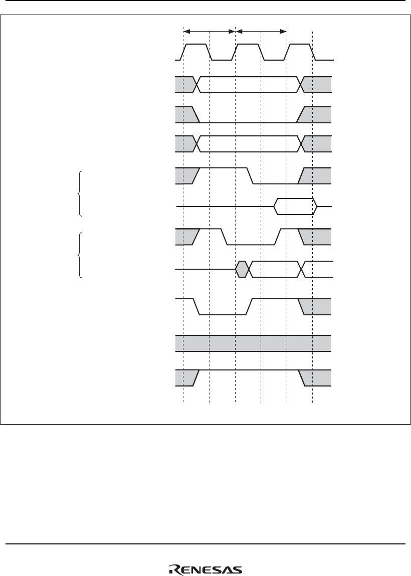
11. Local Bus State Controller (LBSC)
Rev.1.00 Jan. 10, 2008 Page 404 of 1658
REJ09B0261-0100
T1
CLKOUT
A25 to A0
CSn
R/W
RD
D31 to D0
(In reading)
WEn
D31 to D0
(In writing)
BS
T2
RDY
DACKn
In this example, DACKn is high-active.
Figure 11.5 Basic Timing of SRAM Interface
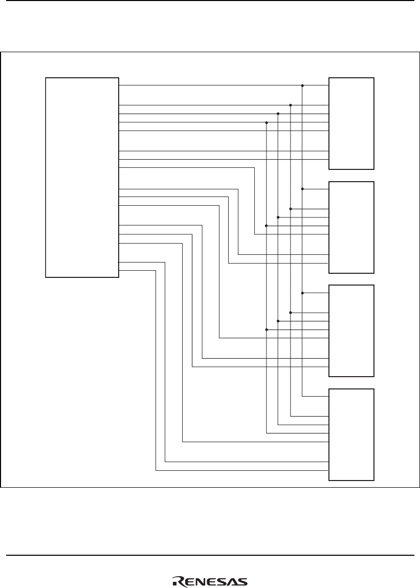
11. Local Bus State Controller (LBSC)
Rev.1.00 Jan. 10, 2008 Page 405 of 1658
REJ09B0261-0100
Figures 11.6 to 11.8 show examples of connections to SRAM with 32-, 16- and 8-bit data width,
respectively.
••••••••••••••••••••
A16
A0
CS
OE
I/O7
I/O0
WE
••••••••
••••
••••
A18
A2
CSn
RD
D31
D24
WE3
D23
D16
WE2
D15
D8
WE1
D7
D0
WE0
SH7785
128K × 8 bits
SRAM
••••
A16
A0
CS
OE
I/O7
I/O0
WE
••••
••••••••
••••
••••
••••
A16
A0
CS
OE
I/O7
I/O0
WE
••••••••
••••
••••
A16
A0
CS
OE
I/O7
I/O0
WE
••••
••••
••••
••••
••••••••
Figure 11.6 Example of 32-Bit Data Width SRAM Connection
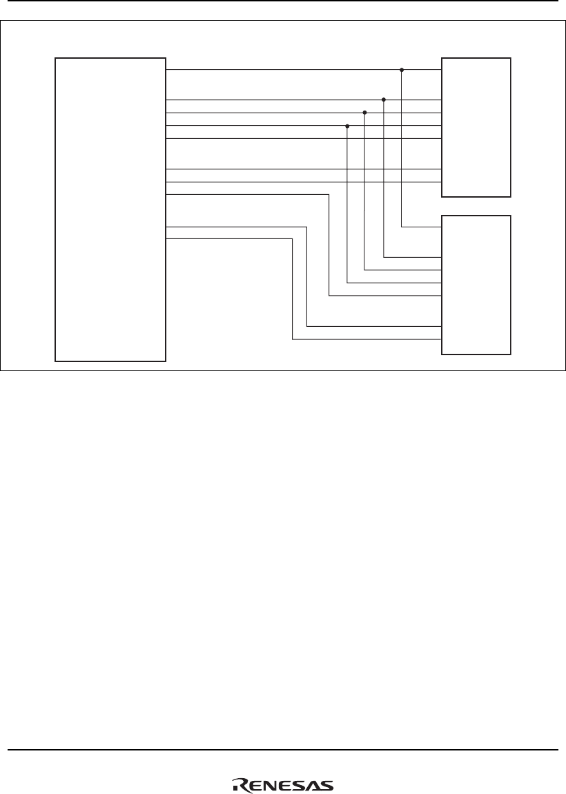
11. Local Bus State Controller (LBSC)
Rev.1.00 Jan. 10, 2008 Page 406 of 1658
REJ09B0261-0100
A16
A0
CS
OE
I/O7
I/O0
WE
A17
A1
CSn
RD
D15
D8
WE1
D7
D0
WE0
SH7785
128K × 8 bits
SRAM
A16
A0
CS
OE
I/O7
I/O0
WE
••••
••••
••••
•••• ••••
••••••••
••••
••••
•••••••• ••••
Figure 11.7 Example of 16-Bit Data Width SRAM Connection

11. Local Bus State Controller (LBSC)
Rev.1.00 Jan. 10, 2008 Page 407 of 1658
REJ09B0261-0100
A16
A0
CSn
RD
D7
D0
WE0
SH7785
128K × 8 bits
SRAM
A16
A0
CS
OE
I/O7
I/O0
WE
••••
••••
••••
••••
••••
••••
••••
••••
Figure 11.8 Example of 8-Bit Data Width SRAM Connection
(2) Wait Cycle Control
Wait cycle insertion for the SRAM interface can be controlled by CSnWCR. If the IW bits in
CSnWCR are set to a value other than 0, a software wait is inserted in accordance with the wait
control bits. For details, see section 11.4.4, CSn Wait Control Register (CSnWCR).
The specified number of Tw cycles is inserted as wait cycles in accordance with the CSnWCR
setting. The wait cycle insertion timing is shown in figure 11.9.
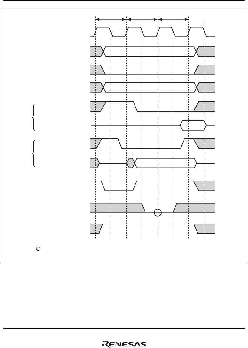
11. Local Bus State Controller (LBSC)
Rev.1.00 Jan. 10, 2008 Page 408 of 1658
REJ09B0261-0100
T1
CLKOUT
A25 to A0
CSn
R/W
RD
D31 to D0
(In reading)
WEn
D31 to D0
(In writing)
BS
Tw T2
RDY
DACKn
In this example, DACKn is active-high. (The circle indicates the sampling timing.)
: Sampling Timing
Figure 11.9 SRAM Interface Wait Timing (Software Wait Only)
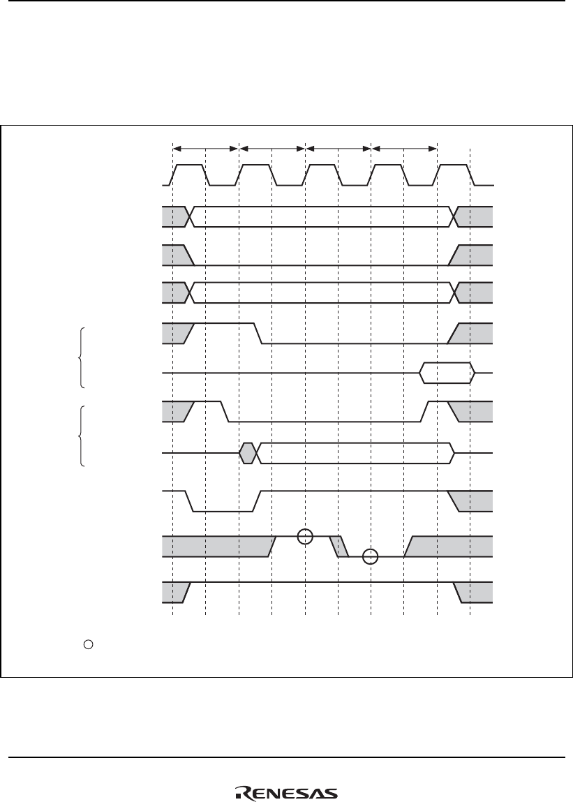
11. Local Bus State Controller (LBSC)
Rev.1.00 Jan. 10, 2008 Page 409 of 1658
REJ09B0261-0100
When software wait insertion is specified by CSnWCR, the external wait input signal, RDY, is
also sampled. The RDY signal sampling timing is shown in figure 11.10, where a single wait cycle
is specified as a software wait. The RDY signal is sampled at the transition from the Tw state to
the T2 state. Therefore, the assertion of the RDY signal has no effect in the T1 cycle or in the first
Tw cycle. The RDY signal is sampled on the rising edge of the clock.
T1
CLKOUT
A25 to A0
CSn
R/W
RD
(In reading)
D31 to D0
(In reading)
WEn
(In writing)
D31 to D0
(In writing)
BS
Tw Twe T2
RDY
DACKn
In this example, DACKn is active-high. (The circles indicate the sampling timing.)
: Sampling Timing
Figure 11.10 SRAM Interface Wait Timing
(Wait Cycle Insertion by RDY Signal, RDY Signal Is Synchronous Input)

11. Local Bus State Controller (LBSC)
Rev.1.00 Jan. 10, 2008 Page 410 of 1658
REJ09B0261-0100
(3) Read-Strobe/Write-Strobe Timing
When the SRAM interface is used, the strobe signal negation timing in reading can be specified
with the RDSPL bit in CSnBCR. For details of settings, see section 11.4.3, CSn Bus Control
Register (CSnBCR). The RDSPL bit should be cleared to 0 when a byte control SRAM is
specified.
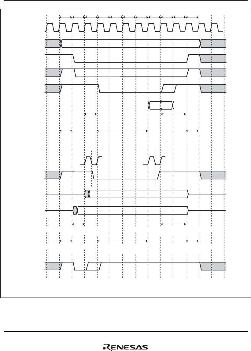
11. Local Bus State Controller (LBSC)
Rev.1.00 Jan. 10, 2008 Page 411 of 1658
REJ09B0261-0100
TAS1
CLKOUT
A25-A0
CSn
R/W
RD
D31-D0
T1 TS1 Tw Tw Tw T2Tw TH1 TH2 TAH1
*1
*2
TS1: CSn assertion - RD assertion delay cycle
CSnWCR RDS = 001
TAS1: Address setup wait
CSnWCR ADS=001
TAH1: Address hold wait
CSnWCR AHS = 001
Tw: Access wait
CSnWCR IW = 0100
TH1, TH2: RD negation - CSn negation delay cycle
CSnWCR RDH = 010
WEn
D31-D0
(ADS=000)
BS
TS1: CSn assertion - WEn assertion delay cycle
CSnWCR WTS = 001
TAS1: Address setup wait
CSnWCR BSH=001
TAH1: Address hold wait
CSnWCR ADH = 001
Tw: Access wait
CSnWCR IW = 0100
TH1, TH2: WE negation - CSn negation delay cycle
CSnWCR WTH = 010
CLKOUT CLKOUT
D31-D0
(ADS=001 to 111)
Notes: 1. When CSnBCR RDSPL is set to 1
2. When CSnWCR BSH is set to 1
Figure 11.11 SRAM Interface Wait Timing (Read-Strobe/Write-Strobe Timing Setting)

11. Local Bus State Controller (LBSC)
Rev.1.00 Jan. 10, 2008 Page 412 of 1658
REJ09B0261-0100
11.5.4 Burst ROM Interface
When the TYPE bit in CSnBCR is set to 010, a burst ROM can be connected to areas 0 to 6. The
burst ROM interface provides high-speed access to ROM that has a burst access function. The
burst access timing of burst ROM is shown in figure 11.12. The wait cycle is set to 0. Although
the access is similar to that of the SRAM interface, only the address is changed when the first
cycle ends and then the next access is started. When 8-bit ROM is used, the number of consecutive
accesses can be set to 4, 8, 16, or 32 times through bits BST2 to BST0 in CSnBCR (n = 0 to 6).
Similarly, when 16-bit ROM is used, 4, 8 or 16 times can be set; when 32-bit ROM is used, 4 or 8
times can be set.
The RDY signal is always sampled when the wait cycle is set to 1 or more. Even when no wait is
specified in the burst ROM settings, the second and subsequent accesses are performed with two
cycles as shown in figure 11.13.
Writing to this interface is performed in the same way as for the SRAM interface.
In a 32-byte transfer, a total of 32 bytes are transferred continuously according to the set bus
width. The first access is performed on the data for which an access request is issued, and the
remaining accesses are performed on wraparound method according to the set bus width. The bus
is not released during this transfer.
Figure 11.14 shows the timing when the burst ROM is used and setup/hold is specified by
CSnWCR.
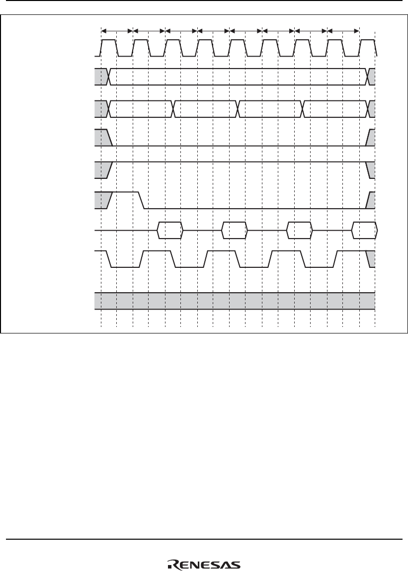
11. Local Bus State Controller (LBSC)
Rev.1.00 Jan. 10, 2008 Page 413 of 1658
REJ09B0261-0100
T1 TB1 TB2 TB1 TB2 TB1TB2 T2
CLKOUT
A25 to A5
A4 to A0
CSn
R/W
RD
D31 to D0
(In reading)
BS
RDY
Figure 11.12 Burst ROM Basic Timing

11. Local Bus State Controller (LBSC)
Rev.1.00 Jan. 10, 2008 Page 414 of 1658
REJ09B0261-0100
T1 Twe TB2 TB1 Tw TB2 TwTw TB1 TB2 Tw T2TB1
CLKOUT
A25 to A5
A4 to A0
CSn
R/W
RD
D31 to D0
(In reading)
BS
RDY
Figure 11.13 Burst ROM Wait Timing
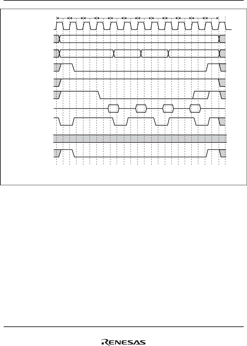
11. Local Bus State Controller (LBSC)
Rev.1.00 Jan. 10, 2008 Page 415 of 1658
REJ09B0261-0100
*2
TAS1 TS1 TB2 TB1 TB2 TB1 TB1T1 TB2 T2 TAH1TH1
CLKOUT
A25 to A5
A4 to A0
CSn
R/W
RD
D31 to D0
(In reading)
BS
RDY
DACKn *1
Notes: 1. In this example, DACKn is active-high.
2. When RDSPL in CSnBCR is set to 1.
Figure 11.14 Burst ROM Wait Timing

11. Local Bus State Controller (LBSC)
Rev.1.00 Jan. 10, 2008 Page 416 of 1658
REJ09B0261-0100
11.5.5 PCMCIA Interface
By setting the TYPE bits in CS5BCR and CS6BCR, the bus interface for the external space areas
5 and 6 can be set to the IC memory card interface or I/O card interface, which is stipulated in
JEIDA specification version 4.2 (PCMCIA 2.1).
Figure 11.15 shows the connection example of this LSI and PCMCIA card. PCMCIA card is
required to connect a three state buffer between this LSI bus interface and PCMCIA card to
perform hot swapping (a card is pulled out or plugged while the power supply of the system is
turned on).
Since operation in big endian mode is not explicitly stipulated in the JEIDA/PCMCIA standard,
this LSI only supports the little-endian PCMCIA interface with the little endian mode setting.
The PCMCIA interface space property can be selected from 8-bit common memory, 16-bit
common memory, 8-bit attribute memory, 16-bit attribute memory, 8-bit I/O space, 16-bit I/O
space, dynamic I/O bus sizing, and ATA complement mode by depending on the setting of the
SAA and SAB bits in CSnPCR.
When the first half area is accessed, the IW bit in CSnWCR and the PCWA, TEDA, and TEHA
bits in CSnPCR are selected. When the second half area is accessed, the IW bit in CSnWCR and
the PCWB, TEDB, and TEHB bits in CSnPCR are selected.
The PCWA/B1 and PCWA/B bits can be used to set the number of wait cycles to be inserted in a
low-speed bus cycle as 0, 15, 30, or 50. This value is added to the number of inserted wait cycles
specified by the IW bit in CSnWCR or PCIW bit in CSnPCR. The setup time of the address of the
RD and WE1 signals, CSn, CE2A, CE2B and REG can be set with the TEDA/B bit (with a setting
range from 0 to 15). The hold time of the address of the RD and WE1 signals, CSn, CE2A, CE2B
and REG can be set with the TEDA/B bit (with a setting range from 0 to 15).
The IW bits (IWW, IWWRD, IWWRS, IWRRD and IWRRS) in CS5BCR or CS6BCR are used to
set the number of idle cycles between cycles. The selected number of wait cycles between cycles
depends only on the area to be accessed (area 5 or 6). When area 5 is accessed, the IW bits in
CS5WCR are selected, and when area 6 is accessed, the IW bits in CS6WCR are selected.
In 32-byte transfer, a total of 32 bytes are transferred continuously according to the set bus width.
The first access is performed on the data for which there was an access request, and the remaining
accesses are performed in wraparound method according to the set bus width. The bus is not
released during this transfer.
ATA complement mode is to access the ATA device register connected to this LSI. The Device
Control Register, Alternate Status Register, Data Register, and Data Port can be accessed in ATA
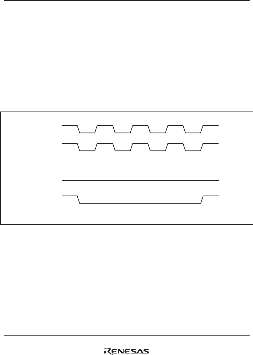
11. Local Bus State Controller (LBSC)
Rev.1.00 Jan. 10, 2008 Page 417 of 1658
REJ09B0261-0100
complement mode. To access the Device Control Register and Alternate Status Register, use a
CPU byte access (do not use a DMA transfer), and to access the Data Register, use the CPU word
access (do not use a DMA transfer). To access the Data Port use a DMA transfer. When a CPU
byte access is executed, CE1x is negated and CE2x is asserted (x = A, B). When a CPU word
access is executed, CE1x is asserted and CE2x is negated. When a DMA access is executed, CE1x
and CE2x are negated. The setting example of the DMAC (by DMA channel control register
CHCR) is external request, burst mode, level detection, overrun 0, DACK output to the
correspondent PCMCIA connected area. Set the DACKBST bit in BCR of the corresponding
DMA transfer channel to 1, so that the corresponding DACK signal is asserted from the beginning
to the end of the DMA transfer cycle. Even if the corresponding DREQ signal is negated during
the transfer, the DACK signal is not negated. When DMA transfer that outputs DACK is made to
access an area where ATA complement mode is set, neither CE1x nor CE2x is asserted.
IO card interface, DACKBST = 0
ATA complement mode, DACKBST = 1
In this example, the number of DMA transfers = 4, transfer size = word, and DACKn is active-low.
CExx
DACKn
CExx
DACKn
Figure 11.15 CExx and DACKn Output during DMA Transfer in Access to Space where
ATA Complement Mode Is Set

11. Local Bus State Controller (LBSC)
Rev.1.00 Jan. 10, 2008 Page 418 of 1658
REJ09B0261-0100
Table 11.16 Relationship between Address and CE when Using PCMCIA Interface
Bus (Bits)
Read/
Write
Access
(bits)*1
Odd/
Even IOIS16 Access CE2 CE1 A0 D15 to D8 D7 to D0
8 Read 8 Even × ⎯ H L L Invalid Read data
Odd × ⎯ H L H Invalid Read data
16 Even × First H L L Invalid Lower read data
Even × Second H L H Invalid Upper read data
Odd × ⎯ ⎯ ⎯ ⎯ ⎯ ⎯
Write 8 Even × ⎯ H L L Invalid Write data
Odd × ⎯ H L H Invalid Write data
16 Even × First H L L Invalid Lower write data
Even × Second H L H Invalid Upper write data
Odd × ⎯ ⎯ ⎯ ⎯ ⎯ ⎯
16 Read 8 Even × ⎯ H L L Invalid Read data
Odd × ⎯ L H H Read data Invalid
16 Even × ⎯ L L L Upper read data Lower read data
Odd × ⎯ ⎯ ⎯ ⎯ ⎯ ⎯
Write 8 Even × ⎯ H L L Invalid Write data
Odd × ⎯ L H H Write data Invalid
16 Even × ⎯ L L L Upper write data Lower write data
Odd × ⎯ ⎯ ⎯ ⎯ ⎯ ⎯
Read 8 Even L ⎯ H L L Invalid Read data
Odd L ⎯ L H H Read data Invalid
Dynamic
Bus Sizing*2
16 Even L ⎯ L L L Upper read data Lower read data
Odd L ⎯ ⎯ ⎯ ⎯ ⎯ ⎯
Write 8 Even L ⎯ H L L Invalid Write data
Odd L ⎯ L H H Write data Invalid
16 Even L ⎯ L L L Upper write data Lower write data
Odd L ⎯ ⎯ ⎯ ⎯ ⎯ ⎯
Read 8 Even H ⎯ H L L Invalid Read data
Odd H First L H H Invalid Invalid
Odd H Second H L L Invalid Read data
16 Even H First L L L Invalid Lower read data
Even H Second H L H Invalid Upper read data
Odd H ⎯ ⎯ ⎯ ⎯ ⎯ ⎯

11. Local Bus State Controller (LBSC)
Rev.1.00 Jan. 10, 2008 Page 419 of 1658
REJ09B0261-0100
Bus (Bits)
Read/
Write
Access
(bits)*1
Odd/
Even IOIS16 Access CE2 CE1 A0 D15 to D8 D7 to D0
Write 8 Even H ⎯ H L L Invalid Write data
Odd H First L H H Invalid Write data
Dynamic
Bus
Sizing*2
Odd H Second H L H Invalid Write data
16 Even H First L L L Upper write data Lower write data
Even H Second H L H Invalid Upper write data
Odd H ⎯ ⎯ ⎯ ⎯ ⎯ ⎯
8 Even × ⎯ L H L Invalid Read data
Odd × ⎯ ⎯ ⎯ ⎯ ⎯ ⎯
ATA
comple-
ment mode
16 Even × ⎯ H L L Upper read data Lower read data
Read
(does
not
output
DACK) Odd × ⎯ ⎯ ⎯ ⎯ ⎯ ⎯
8 Even × ⎯ L H L Invalid Write data
Odd × ⎯ ⎯ ⎯ ⎯ ⎯ ⎯
16 Even × ⎯ H L L Upper write data Lower write data
Write
(does
not
output
DACK) Odd × ⎯ ⎯ ⎯ ⎯ ⎯ ⎯
8 Even × ⎯ H H L Invalid Read data
Odd × ⎯ H H L Read data Invalid
16 Even × ⎯ H H H Upper read data Lower read data
Read
(outputs
DACK)
Odd × ⎯ ⎯ ⎯ ⎯ ⎯ ⎯
8 Even × ⎯ H H L Invalid Write data
Odd × ⎯ H H L Write data Invalid
Write
(outputs
DACK)
16 Even × ⎯ H H H Upper write data Lower write data
Odd × ⎯ ⎯ ⎯ ⎯ ⎯ ⎯
Legend:
×: Don't care
L: Low level
H: High level
Notes: 1. In 32-bit/64-bit/16-byte/32-byte transfer, the address is automatically incremented by
the bus width, and the above accesses are repeated until the transfer data size is
reached.
2. PCMCIA I/O card interface only.
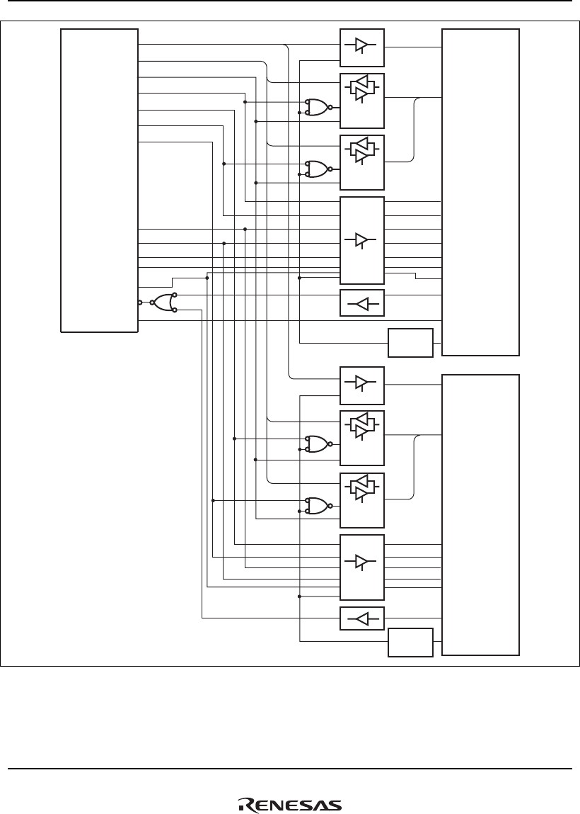
11. Local Bus State Controller (LBSC)
Rev.1.00 Jan. 10, 2008 Page 420 of 1658
REJ09B0261-0100
G
A25 to A0
D15 to D0
PC card
(memory I/O)
CD1, CD2
CE1
G
CE2
OE
WE/PGM
(IORD)
(IOWR)
(IOIS6)
WAIT
A25 to A0
D15 to D0
PC card
(memory I/O)
CD1, CD2
CE1
CE2
OE
WE/PGM
WAIT
A25 to A0
SH7785
D15 to D0
R/W
CE2B
CE2A
RD
WE1
CE1B/(CS6)
CE1A/(CS5)
ICIORD
ICIOWR
RDY
IOIS16
G
DIR
D7 to D0
D15 to D8
G
DIR
G
G
G
DIR
G
DIR
D7 to D0
Card
detection
circuit
Card
detection
circuit
D15 to D8
REGREG
REG
Figure 11.16 Example of PCMCIA Interface
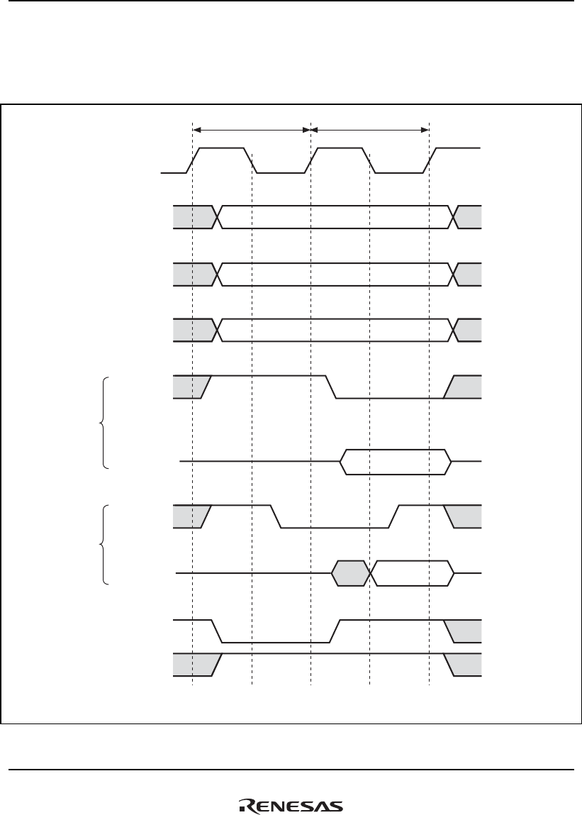
11. Local Bus State Controller (LBSC)
Rev.1.00 Jan. 10, 2008 Page 421 of 1658
REJ09B0261-0100
(1) Memory Card Interface Basic Timing
Figure 11.17 shows the basic timing for the PCMCIA memory card interface, and figure 11.18
shows the wait timing for the PCMCIA memory card interface.
CLKOUT
Tpcm1 Tpcm2
A25 to A0
CExx
R/W
D15 to D0
(In reading)
D15 to D0
(In writing)
RD
(In reading)
WE1
(In writing)
BS
REG
DACKn
(DA)
In this example, DACKn is active-high.
Figure 11.17 Basic Timing for PCMCIA Memory Card Interface
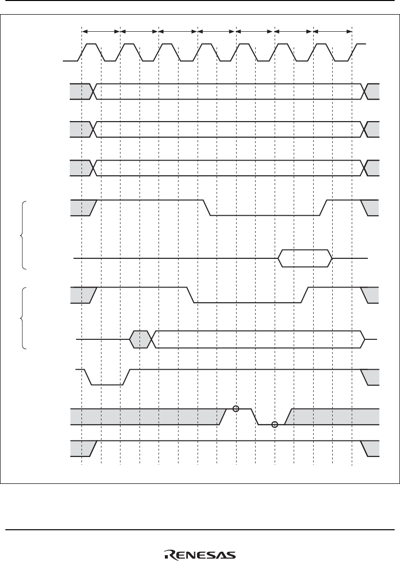
11. Local Bus State Controller (LBSC)
Rev.1.00 Jan. 10, 2008 Page 422 of 1658
REJ09B0261-0100
CLKOUT
Tpcm0
A25 to A0
R/W
CExx
REG
RD
(In reading)
D15 to D0
(In reading)
D15 to D0
(In writing)
WE1
(In writing)
BS
RDY
Tpcm0w Tpcm1 Tpcm1w Tpcm1w Tpcm2 Tpcm2w
DACKn
In this example, DACKn is active-high.
Figure 11.18 Wait Timing for PCMCIA Memory Card Interface

11. Local Bus State Controller (LBSC)
Rev.1.00 Jan. 10, 2008 Page 423 of 1658
REJ09B0261-0100
(2) I/O Card Interface Timing
Figures 11.19 and 11.20 show the timing for the PCMCIA I/O card interface.
When a PCMCIA card is accessed as the I/O card interface, dynamic sizing with the I/O bus width
can be performed using the IOIS16 pin. With the 16-bit bus width selected, if the IOIS16 signal is
high during the word-size I/O bus cycle, the I/O port is recognized as eight bits in bus width. In
this case, a data access for only eight bits is performed in the I/O bus cycle being executed, and
this is automatically followed by a data access for the remaining eight bits. Dynamic bus sizing is
also performed for byte-size access to address 2n + 1.
Figure 11.21 shows the basic timing for dynamic bus sizing.
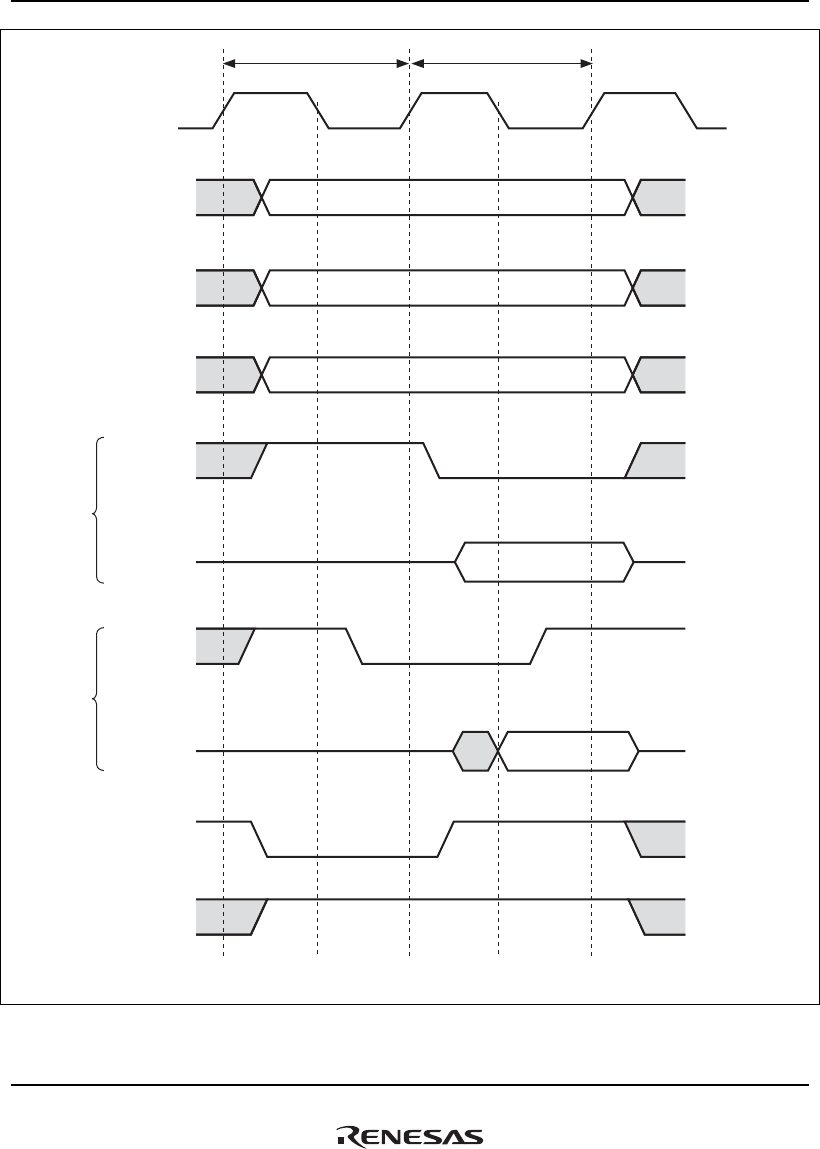
11. Local Bus State Controller (LBSC)
Rev.1.00 Jan. 10, 2008 Page 424 of 1658
REJ09B0261-0100
CLKOUT
Tpci1 Tpci2
A25 to A0
R/W
CExx
ICIORD
(In reading)
D15 to D0
(In reading)
ICIOWR
(In writing)
D15 to D0
(In writing)
BS
REG
DACKn
In this example, DACKn is active-high.
Figure 11.19 Basic Timing for PCMCIA I/O Card Interface
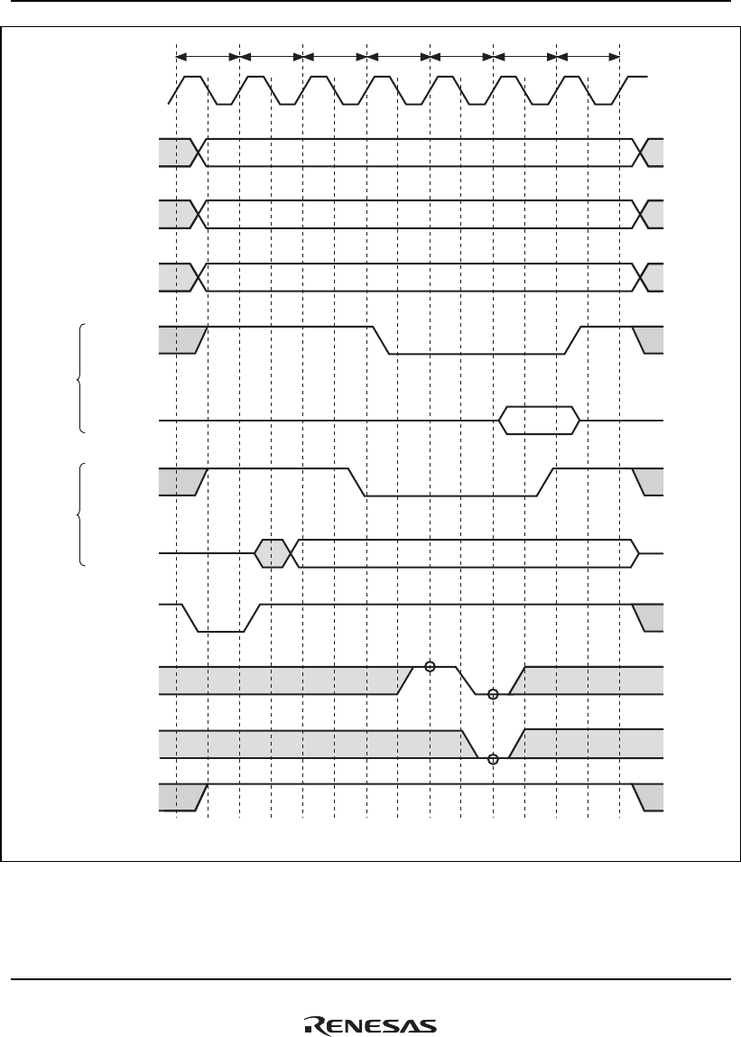
11. Local Bus State Controller (LBSC)
Rev.1.00 Jan. 10, 2008 Page 425 of 1658
REJ09B0261-0100
CLKOUT
A25 to A0
R/W
CExx
ICIORD
(In reading)
ICIOWR
(In writing)
D15 to D0
(In reading)
D15 to D0
(In writing)
BS
RDY
IOIS16
Tpci0 Tpci0w Tpci1 Tpci1wTpci1w Tpci2 Tpci2w
REG
DACKn
In this example, DACKn is active-high.
Figure 11.20 Wait Timing for PCMCIA I/O Card Interface
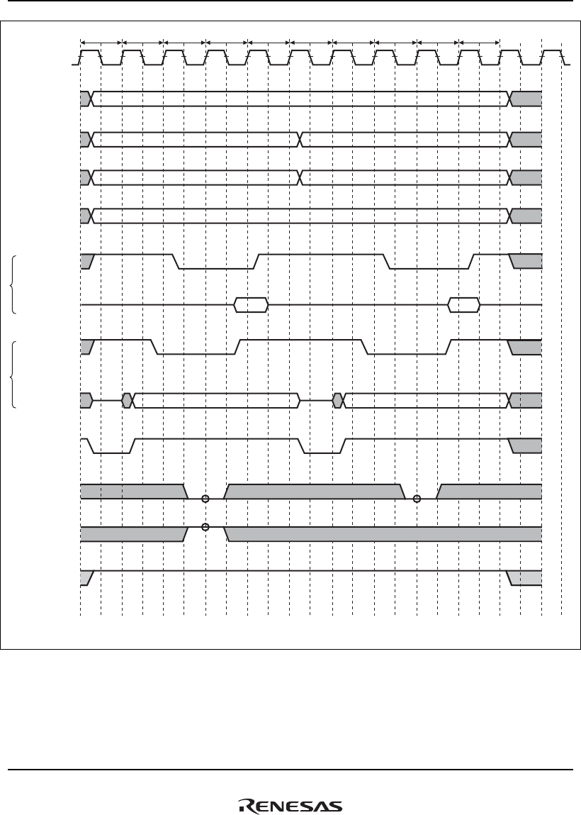
11. Local Bus State Controller (LBSC)
Rev.1.00 Jan. 10, 2008 Page 426 of 1658
REJ09B0261-0100
TpciTpci0 Tpci1w Tpci2 Tpci2w Tpci0 Tpci Tpci2
Tpci1w Tpci2w
CLKOUT
A25 to A1
A0
R/W
IORD (WE2)
(In reading)
IOWR (WE3)
(In writing)
D15 to D0
(In writing)
D15 to D0
(In reading)
BS
IOIS16
DACKn
CExx
REG
RDY
In this example, DACKn is active-high.
Figure 11.21 Dynamic Bus Sizing Timing for PCMCIA I/O Card Interface

11. Local Bus State Controller (LBSC)
Rev.1.00 Jan. 10, 2008 Page 427 of 1658
REJ09B0261-0100
11.5.6 MPX Interface
When both the MODE 7 pin is set to 0 at a power-on reset by the PRESET pin, the MPX interface
is selected for area 0. The MPX interface is selected for areas 1 to 6 by the MPX bit in CS1BCR,
CS2BCR, and CS4BCR to CS6BCR. The MPX interface provides an address/data multiplex-type
bus protocol and facilitates connection with external memory controller chips using an
address/data multiplex-type 64- or 32-bit single bus. A bus cycle consists of an address phase and
a data phase. In the address phase, address information is output on D25 to D0, and the access size
is output on D63 to D61 for the 64-bit bus and on D31 to D29 for the 32-bit bus. The BS signal is
asserted for one cycle to indicate the address phase. The CSn signal is asserted at the rising edge in
Tm1 and is negated after the end of the last data transfer in the data phase. Therefore, a negation
cycle is not generated in the case of minimum pitch access. The FRAME signal is asserted at the
rising edge in Tm1 and negated at the start of the last data transfer cycle in the data phase.
Therefore, an external device for the MPX interface must internally store the address information
and access size output in the address phase and perform data input/output for the data phase. For
details, see section 11.5.1, Endian/Access Size and Data Alignment.
Values output to address pins A25 to A0 are not guaranteed.
In 32-byte transfer, a total of 32 bytes are transferred continuously according to the set bus width.
The first access is performed on the data for which an access request is issued, and the remaining
accesses are performed according to the set bus width. If the access size is larger than the bus
width, a burst access with continuing multiple data cycles occurs after one address output. The bus
is not released during this transfer.
Table 11.17 Relationship between D63/D31 to D61/D29 and Access Size in Address Phase
D63/D31 D62/D30 D61/D29 Access Size
0 0 0 Byte
1 Word
1 0 Longword
1 Unused
1 X X 32-byte burst
Legend:
X: Don't care
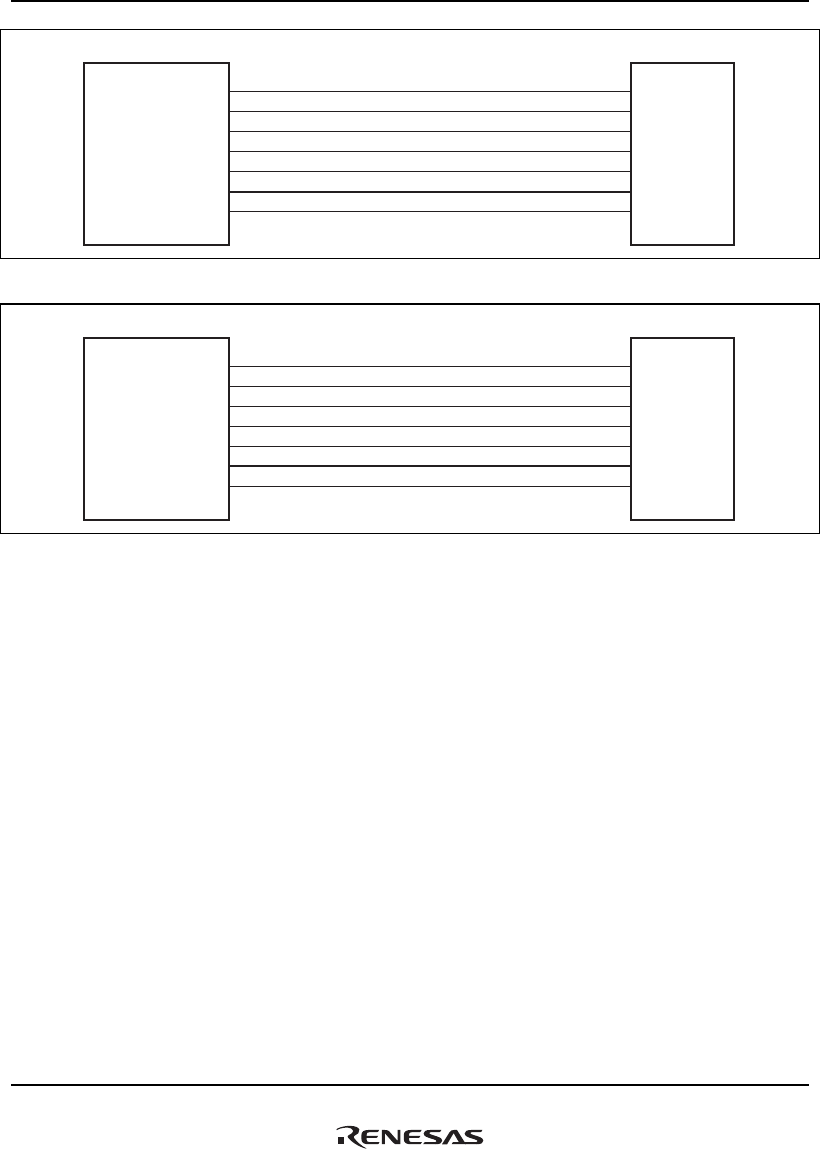
11. Local Bus State Controller (LBSC)
Rev.1.00 Jan. 10, 2008 Page 428 of 1658
REJ09B0261-0100
CLKOUT
CSn
BS
RD
R/W
D31 to D0
RDY
SH7785 MPX device
CLK
CS
BS
FRAME
WE
I/O31 to I/O0
RDY
Figure 11.22 Example of 32-Bit Data Width MPX Connection
CLKOUT
CSn
BS
RD
RD/WR
D63 to D0
RDY
SH7785 MPX device
CLK
CS
BS
FRAME
WE
I/O63 to I/O0
RDY
Figure 11.23 Example of 64-Bit Data Width MPX Connection
The MPX interface timing is shown below.
When the MPX interface is used for area 0, the bus size should be set to 64 or 32 bits by MODE5
and MODE6. When the MPX interface is used for areas 1 to 6, the bus size should be set to 32 or
64 bits by CSnBCR.
Waits can be inserted by CSnWCR and the RDY pin.
In reading, one wait cycle is automatically inserted after address output even if CSnWCR is
cleared to 0.
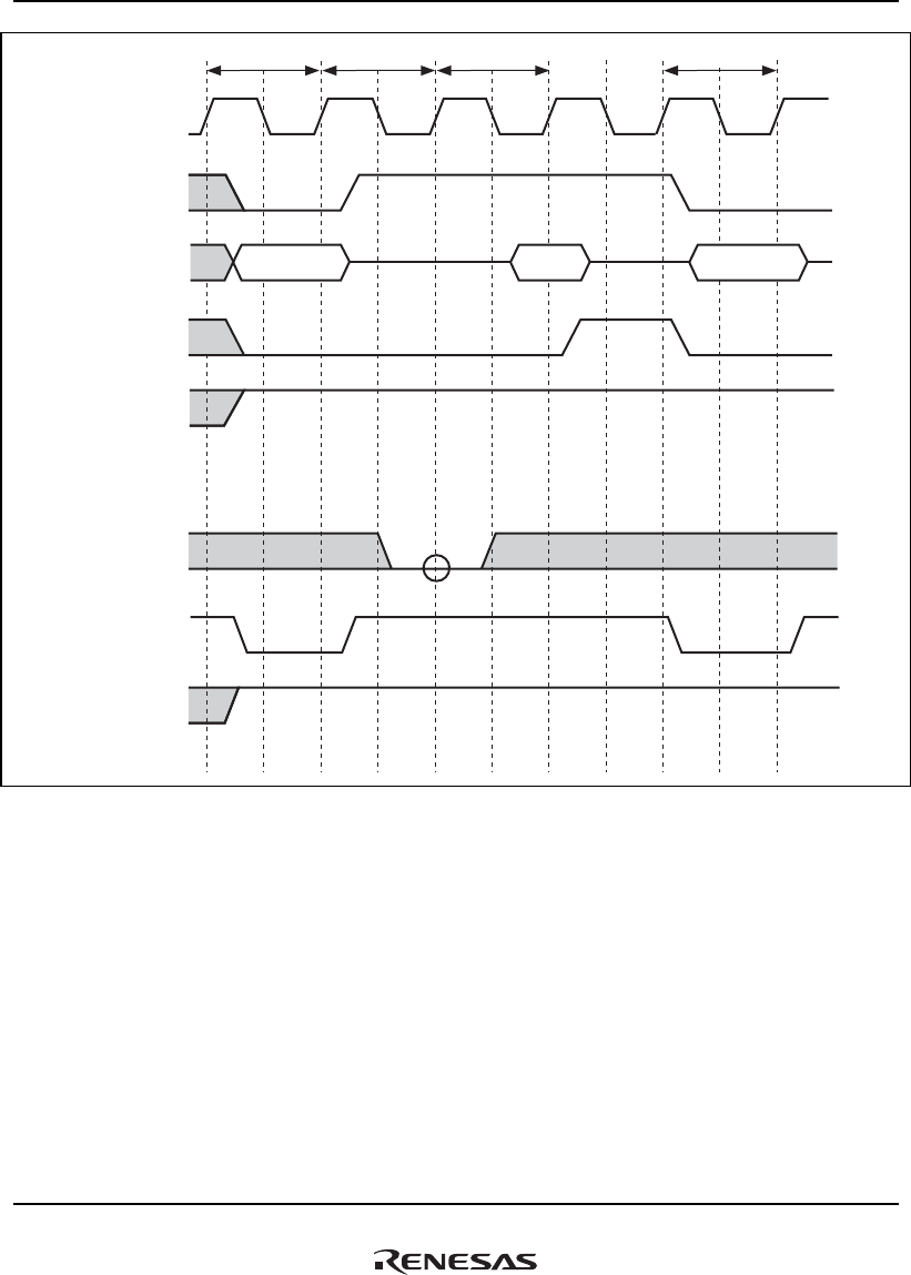
11. Local Bus State Controller (LBSC)
Rev.1.00 Jan. 10, 2008 Page 429 of 1658
REJ09B0261-0100
Tm1 Tm1
CLKOUT
RD/FRAME
CSn
R/W
D63 to D0
BS
Tmd1w Tmd1
RDY
DACK
AD0A
Figure 11.24 MPX Interface Timing 1
(Single Read Cycle, IW = 0000, No External Wait, 64-Bit Bus Width)
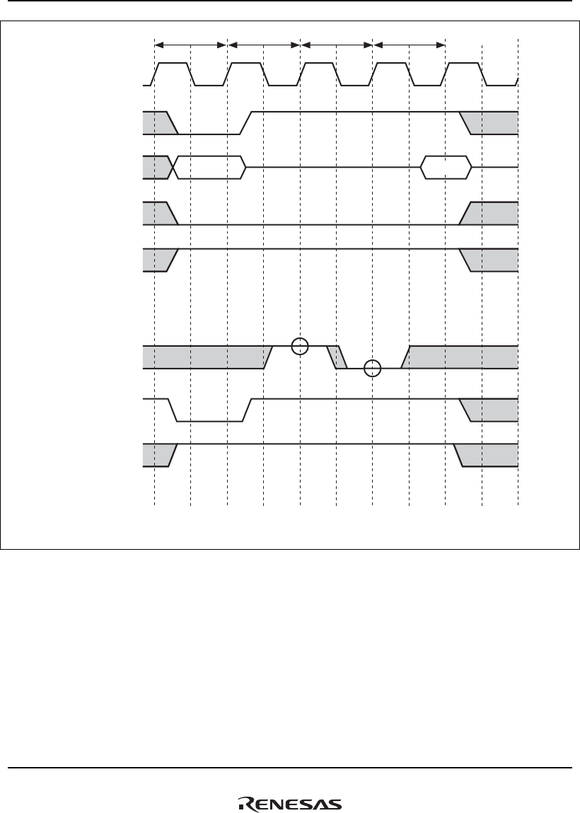
11. Local Bus State Controller (LBSC)
Rev.1.00 Jan. 10, 2008 Page 430 of 1658
REJ09B0261-0100
Tm1
CLKOUT
A
RD/FRAME
CSn
R/W
D63 to D0
BS
Tmd1w Tmd1w Tmd1
RDY
DACKn
D0
In this example, DACKn is active-high. The circles indicate the sampling timing.
Figure 11.25 MPX Interface Timing 2
(Single Read, IW = 0000, One External Wait Inserted, 64-Bit Bus Width)
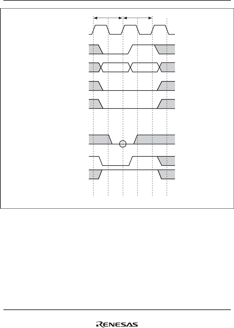
11. Local Bus State Controller (LBSC)
Rev.1.00 Jan. 10, 2008 Page 431 of 1658
REJ09B0261-0100
Tm1
CLKOUT
A
RD/FRAME
CSn
R/W
D63 to D0
BS
Tmd1
RDY
DACKn
D0
In this example, DACKn is active-high. The circle indicates the sampling timing.
Figure 11.26 MPX Interface Timing 3
(Single Write Cycle, IW = 0000, No External Wait, 64-Bit Bus Width)
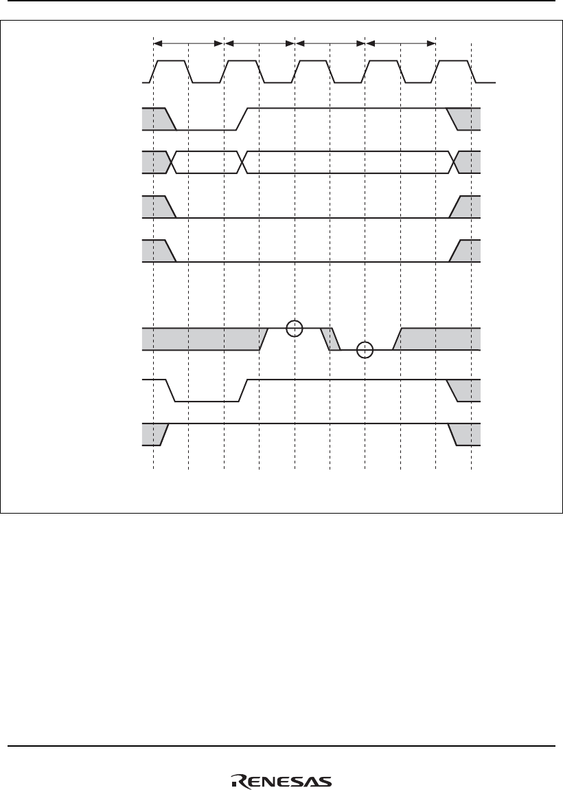
11. Local Bus State Controller (LBSC)
Rev.1.00 Jan. 10, 2008 Page 432 of 1658
REJ09B0261-0100
Tm1
CLKOUT
A
RD/FRAME
CSn
R/W
D63 to D0
BS
Tmd1w Tmd1w Tmd1
RDY
DACKn
D0
In this example, DACKn is active-high.
Figure 11.27 MPX Interface Timing 4
(Single Write Cycle, IW = 0001, One External Wait Inserted, 64-Bit Bus Width)
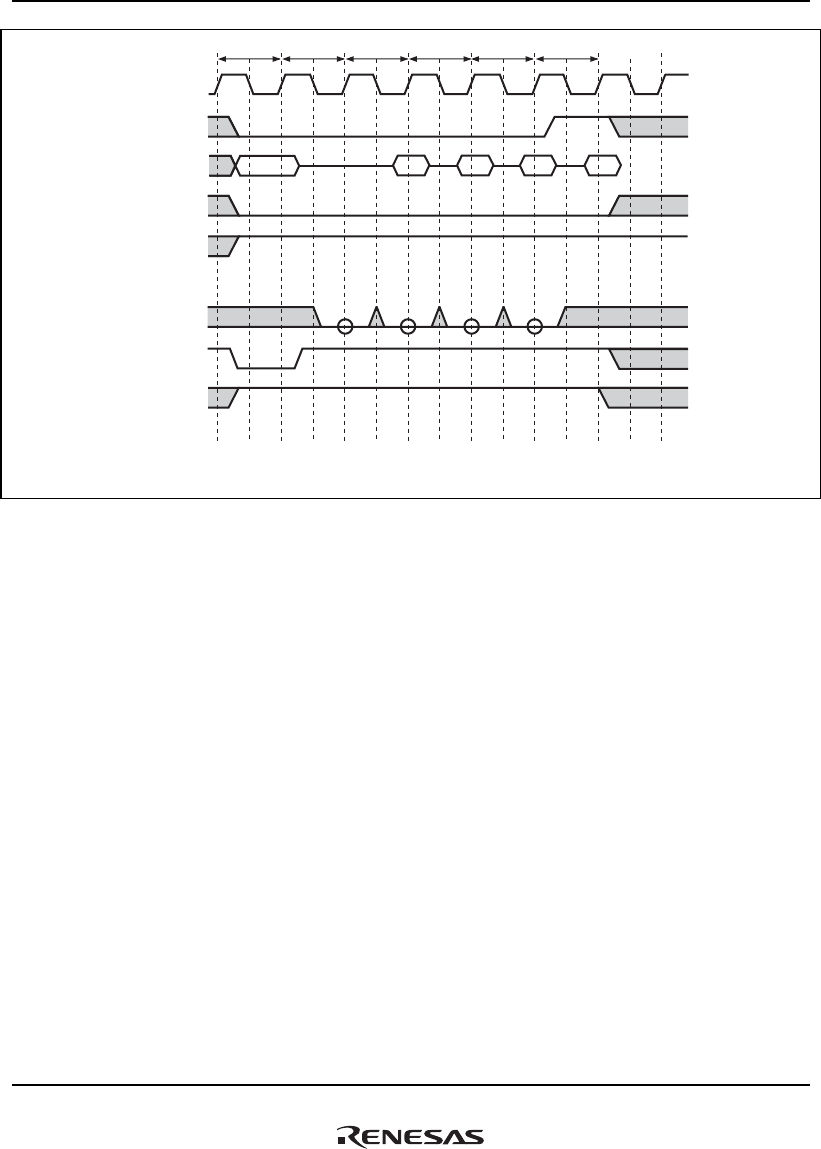
11. Local Bus State Controller (LBSC)
Rev.1.00 Jan. 10, 2008 Page 433 of 1658
REJ09B0261-0100
Tm1
CLKOUT
RD/FRAME
CSn
R/W
D63 to D0
BS
Tmd1w Tmd1 Tmd2 Tmd3 Tmd4
RDY
DACKn
D1 D2 D3D0
A
In this example, DACKn is active-high.
Figure 11.28 MPX Interface Timing 5
(Burst Read Cycle, IW = 0000, No External Wait, 64-Bit Bus Width, 32-Byte Data Transfer)

11. Local Bus State Controller (LBSC)
Rev.1.00 Jan. 10, 2008 Page 434 of 1658
REJ09B0261-0100
Tm1
CLKOUT
A
RD/FRAME
CSn
R/W
D63 to D0
BS
Tmd1w Tmd1 Tmd2w Tmd2 Tmd3 Tmd4w Tmd4
RDY
DACKn
D3D1 D2D0
In this example, DACKn is active-high.
Figure 11.29 MPX Interface Timing 6 (Burst Read Cycle, IW = 0000,
External Wait Control, 64-Bit Bus Width, 32-Byte Data Transfer)
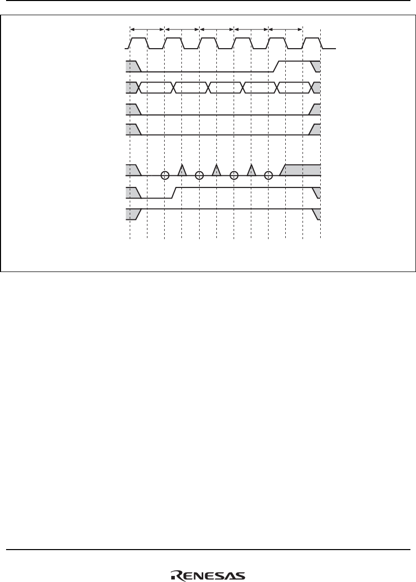
11. Local Bus State Controller (LBSC)
Rev.1.00 Jan. 10, 2008 Page 435 of 1658
REJ09B0261-0100
Tm1
CLKOUT
A
RD/FRAME
CSn
R/W
D63 to D0
BS
Tmd1 Tmd2 Tmd3 Tmd4
RDY
DACKn
D0 D1 D2 D3
In this example, DACKn is active-high.
Figure 11.30 MPX Interface Timing 7
(Burst Write Cycle, IW = 0000, No External Wait, 64-Bit Width, 32-Byte Data Transfer)
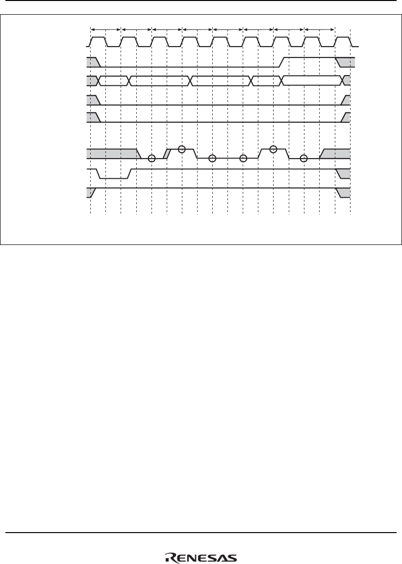
11. Local Bus State Controller (LBSC)
Rev.1.00 Jan. 10, 2008 Page 436 of 1658
REJ09B0261-0100
D2
D1
Tm1
CLKOUT
A
RD/FRAME
CSn
R/W
D63 to D0
BS
Tmd1w Tmd1 Tmd2w Tmd2 Tmd3 Tmd4w Tmd4
RDY
DACKn
D0 D3
In this example, DACKn is active-high.
Figure 11.31 MPX Interface Timing 8 (Burst Write Cycle, IW = 0001,
External Wait Control, 32-Bit Bus Width, 32-Byte Data Transfer)
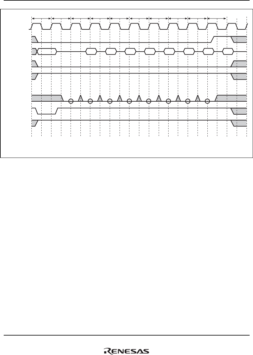
11. Local Bus State Controller (LBSC)
Rev.1.00 Jan. 10, 2008 Page 437 of 1658
REJ09B0261-0100
Tm1
CLKOUT
RD/FRAME
CSn
R/W
D31 to D0
BS
Tmd1w Tmd1 Tmd2 Tmd3 Tmd4 Tmd5 Tmd6 Tmd7 Tmd8
RDY
DACKn
A
In this example, DACKn is active-high.
D2 D3D1 D4 D6 D7 D8D5
Figure 11.32 MPX Interface Timing 9 (Burst Read Cycle, IW = 0000,
No External Wait, 32-Bit Bus Width, 32-Byte Data Transfer)
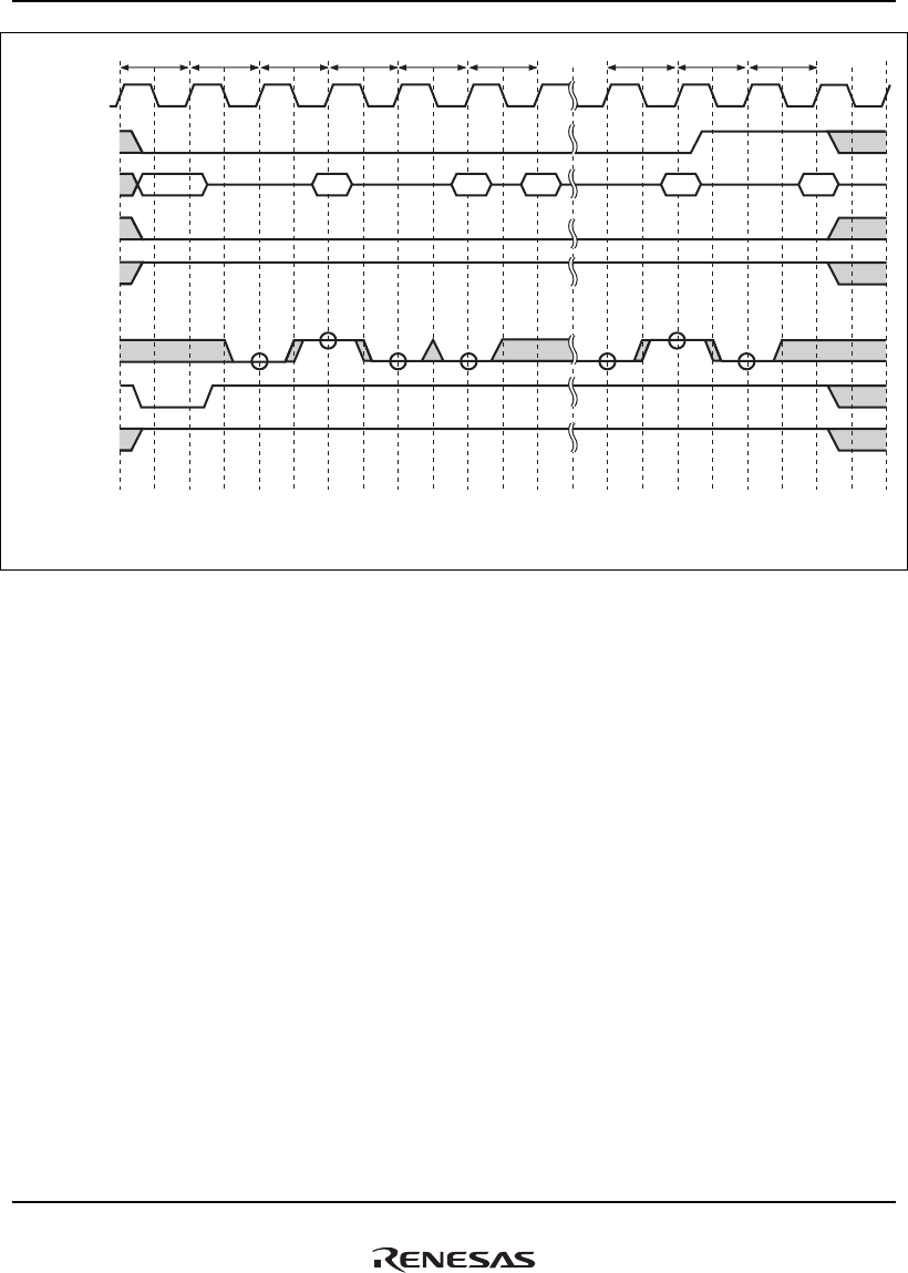
11. Local Bus State Controller (LBSC)
Rev.1.00 Jan. 10, 2008 Page 438 of 1658
REJ09B0261-0100
Tm1
CLKOUT
A
RD/FRAME
CSn
R/W
D31 to D0
BS
Tmd1w Tmd1 Tmd2w Tmd2 Tmd3 Tmd7 Tmd8w Tmd8
RDY
DACKn
D7 D8D2 D3D1
In this example, DACKn is active-high.
Figure 11.33 MPX Interface Timing 10 (Burst Read Cycle, IW = 0000,
External Wait Control, 32-Bit Bus Width, 32-Byte Data Transfer)
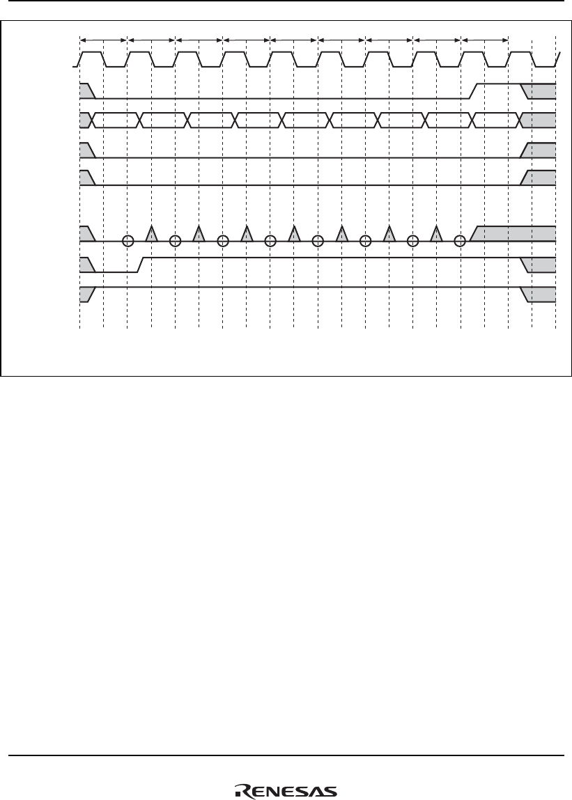
11. Local Bus State Controller (LBSC)
Rev.1.00 Jan. 10, 2008 Page 439 of 1658
REJ09B0261-0100
Tm1
CLKOUT
A
RD/FRAME
CSn
R/W
D31 to D0
BS
Tmd1 Tmd2 Tmd3 Tmd4 Tmd5 Tmd6 Tmd7 Tmd8
RDY
DACKn
D1 D2 D3 D4 D5 D6 D7 D8
In this example, DACKn is active-high.
Figure 11.34 MPX Interface Timing 11 (Burst Write Cycle, IW = 0000,
No External Wait, 32-Bit Bus Width, 32-Byte Data Transfer)
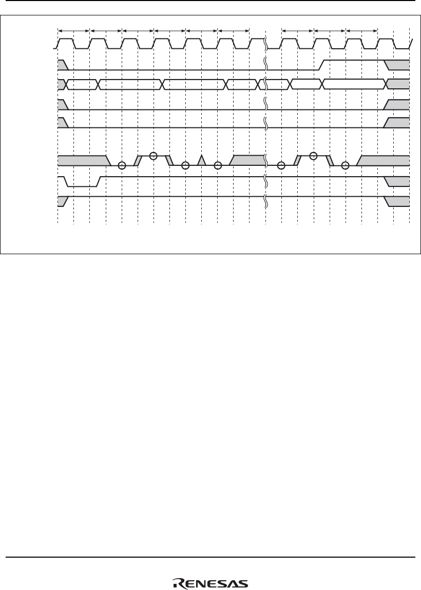
11. Local Bus State Controller (LBSC)
Rev.1.00 Jan. 10, 2008 Page 440 of 1658
REJ09B0261-0100
D3
D2
Tm1
CLKOUT
A
RD/FRAME
CSn
R/W
D31 to D0
BS
Tmd1w Tmd1 Tmd2w Tmd2 Tmd3 Tmd7 Tmd8w Tmd8
RDY
DACKn
D1 D7 D8
In this example, DACKn is active-high.
Figure 11.35 MPX Interface Timing 12 (Burst Write Cycle, IW = 0001,
External Wait Control, 32-Bit Bus Width, 32-Byte Data Transfer)

11. Local Bus State Controller (LBSC)
Rev.1.00 Jan. 10, 2008 Page 441 of 1658
REJ09B0261-0100
11.5.7 Byte Control SRAM Interface
The byte control SRAM interface is a memory interface that outputs a byte-select strobe (WEn) in
both read and write bus cycles. This interface has 16-bit data pins and can be connected to SRAM
having an upper byte select strobe and lower select strobe functions such as UB and LB.
Areas 1 and 4 can be specified as a byte control SRAM interface.
The write timing for the byte control SRAM interface is identical to that of a normal SRAM
interface.
In reading operation, on the other hand, the WEn pin timing is different. In a read access, only the
WEn signal for the byte being read is asserted. Assertion is synchronized with the falling edge of
the CLKOUT clock in the same way as for the WEn signal, while negation is synchronized with
the rising edge of the CLKOUT clock in the same way as for the RD signal.
In 32-byte transfer, a total of 32 bytes are transferred continuously according to the set bus width.
The first access is performed on the data for which there was an access request, and the remaining
accesses are performed in wraparound method according to the set bus width. The bus is not
released during this transfer.
Figures 11.36 and 11.37 show examples of byte control SRAM connections, and figures 11.38 to
11.40 show examples of byte-control SRAM read cycles.
A17 to A2
CSn
RD
R/W
SH7785
64K × 16 bits
SRAM
D15 to D0
WE1
WE0
A15 to A0
CS
OE
WE
I/O15 to I/O0
UB
LB
A15 to A0
CS
OE
WE
I/O15 to I/O0
UB
LB
D31 to D16
WE3
WE2
Figure 11.36 Example of Byte Control SRAM with 32-Bit Data Width
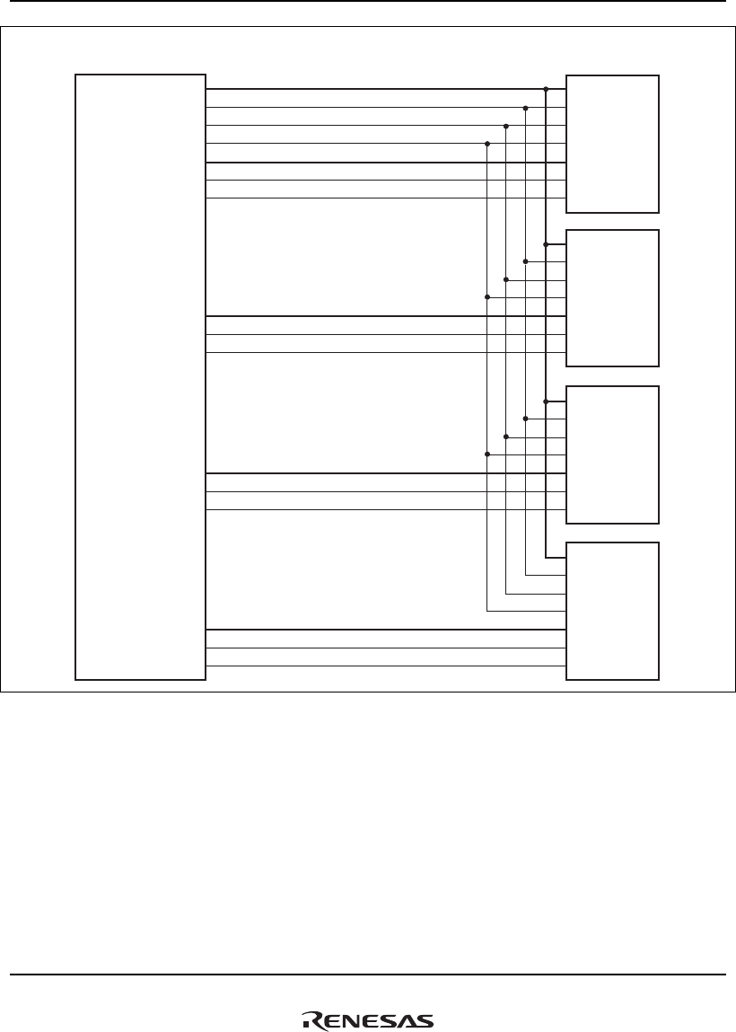
11. Local Bus State Controller (LBSC)
Rev.1.00 Jan. 10, 2008 Page 442 of 1658
REJ09B0261-0100
A18 to A3
CSn
RD
R/W
SH7785
64K × 16 bits
SRAM
D47 to D32
WE5
WE4
D31 to D16
WE3
WE2
D15 to D0
WE1
WE0
A15 to A0
CS
OE
WE
I/O15 to I/O0
UB
LB
A15 to A0
CS
OE
WE
I/O15 to I/O0
UB
LB
A15 to A0
CS
OE
WE
I/O15 to /O0
UB
LB
A15 to A0
CS
OE
WE
I/O15 to I/O0
UB
LB
D63 to D48
WE7
WE6
Figure 11.37 Example of Byte Control SRAM with 64-Bit Data Width
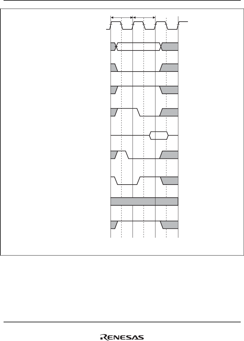
11. Local Bus State Controller (LBSC)
Rev.1.00 Jan. 10, 2008 Page 443 of 1658
REJ09B0261-0100
T1 T2
CLKOUT
A25 to A0
CSn
R/W
RD
D31 to D0
(In reading)
BS
DACKn
RDY
WEn
In this example, DACKn is active-high.
Figure 11.38 Basic Read Cycle of Byte Control SRAM (No Wait)
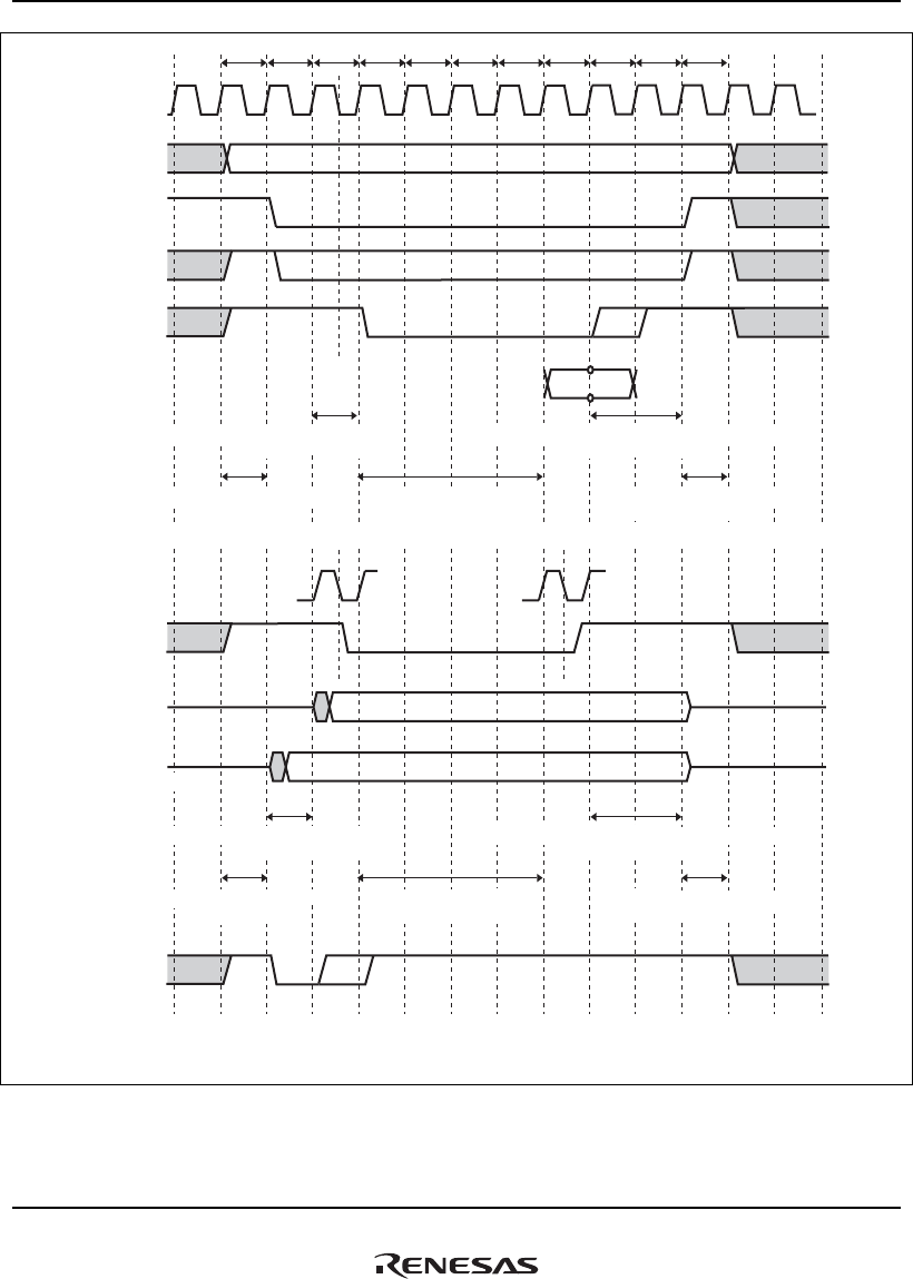
11. Local Bus State Controller (LBSC)
Rev.1.00 Jan. 10, 2008 Page 444 of 1658
REJ09B0261-0100
TAS1
CLKOUT
A25-A0
CSn
R/W
WEn
(In reading)
(In writing)
D63-D0
T1 TS1 Tw Tw Tw T2Tw TH1 TH2 TAH1
*1
*2
TS1: CSn assertion - RD assertion delay cycle
CSnWCR RDS = 001
TAS1: Address setup wait
CSnWCR ADS=001
TAH1: Address hold wait
CSnWCR AHS = 001
Tw: Access wait
CSnWCR IW = 0100
TH1, TH2: RD negation - CSn negation delay cycle
CSnWCR RDH = 010
WEn
D63 to D0
(ADS=000)
BS
TS1: CSn assertion - WEn assertion delay cycle
CSnWCR WTS = 001
TAS1: Address setup wait
CSnWCR BSH=001
TAH1: Address hold wait
CSnWCR ADH = 001
Tw: Access wait
CSnWCR IW = 0100
TH1, TH2: WE negation - CSn negation delay cycle
CSnWCR WTH = 010
CLKOUT CLKOUT
D63 to D0
(ADS=001 to 111)
Notes: 1. When CSnBCR RDSPL is set to 1
2. When CSnWCR BSH is set to 1
Figure 11.39 Wait State Timing of Byte Control SRAM
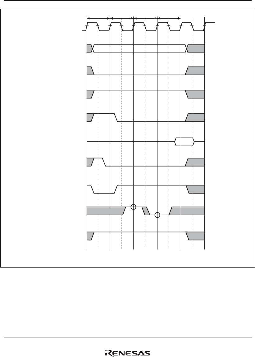
11. Local Bus State Controller (LBSC)
Rev.1.00 Jan. 10, 2008 Page 445 of 1658
REJ09B0261-0100
T1 Tw Twe T2
CLKOUT
A25 to A0
CSn
R/W
RD
D31 to D0
(In reading)
BS
DACKn
RDY
WEn
In this example, DACKn is active-high.
Figure 11.40 Wait State Timing of Byte Control SRAM
(One Internal Wait + One External Wait)

11. Local Bus State Controller (LBSC)
Rev.1.00 Jan. 10, 2008 Page 446 of 1658
REJ09B0261-0100
11.5.8 Wait Cycles between Access Cycles
When the external memory bus operating frequency is high, the turn-off of the data buffer
performed on completion of reading from a low-speed device may not be made in time. This cause
a collision with the next access data or a malfunction, which results in lower reliability. To prevent
this problem, the data collision prevention function is provided. With this function, the preceding
access area and the type of read/write are stored and a wait cycle is inserted before the access
cycle if there is a possibility that a bus collision occurs when the next access is started. As an
example of wait cycle insertion, idle cycles are inserted between the access cycles as shown in
section 11.4.3, CSn Bus Control Register (CSnBCR). By using bits IWW, IWRWD, IWRWS,
IWRRD and IWRRS in CSnBCR, at least the specified number of cycles can be inserted as idle
cycles.
When bus arbitration is performed, the bus is released after wait cycles are inserted between the
cycles.
When DMA transfer is performed in dual address mode, wait cycles are inserted as set in
CSnBCR idle cycle bits.
When consecutive accesses to the MPX interface area are performed after a read access, 1 wait
cycle is inserted even if the wait cycle is set to 0.
When the access size is 8-byte or 16-byte, wait cycles are inserted every 4-byte access.
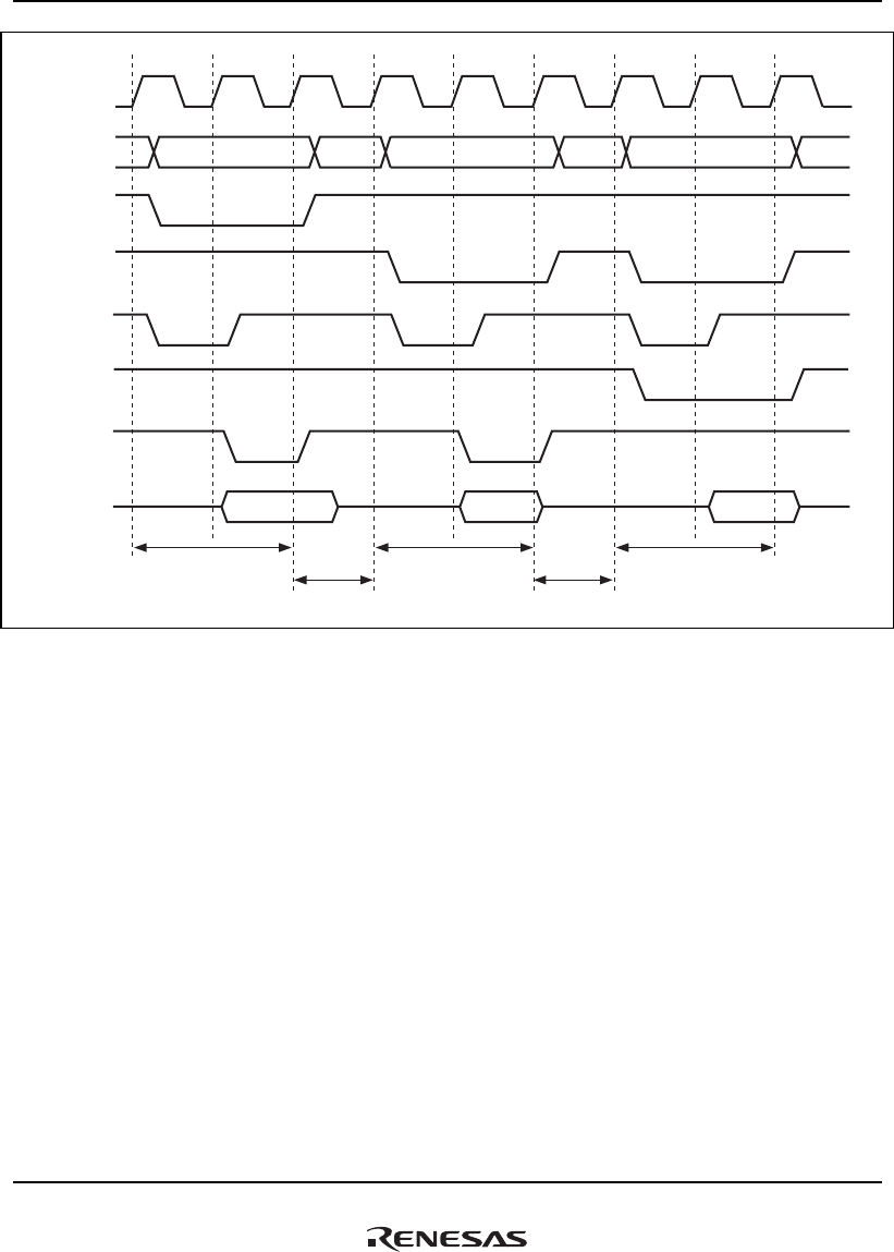
11. Local Bus State Controller (LBSC)
Rev.1.00 Jan. 10, 2008 Page 447 of 1658
REJ09B0261-0100
T1
CLKOUT
CSm
CSn
A25 to A0
BS
R/W
RD
D31 to D0
T2 Twait T1 T2 Twait T1 T2
Reading area m space
CSnBCR.IWRRD=001 CSnBCR.IWRWS=001
Reading area n space Writing area n space
Figure 11.41 Wait Cycles between Access Cycles (Access Size Is 4 Bytes)

11. Local Bus State Controller (LBSC)
Rev.1.00 Jan. 10, 2008 Page 448 of 1658
REJ09B0261-0100
11.5.9 Bus Arbitration
This LSI is provided with a bus arbitration function that gives the bus to an external device when a
request is issued from the device.
This bus arbitration supports master mode and slave mode. In master mode the bus is held on a
steady state, and is released to another device in response to a bus request. In slave mode, the bus
is not held in the steady state. Each time the external bus cycle occurs, the bus mastership is
required, and the bus is released after completion of access.
Master mode and slave mode are specified by the external mode pin settings. In master mode and
slave mode, the bus enters the high-impedance state when not being held. In master mode, it is
possible to connect an external device that issues bus requests. In the following description, an
external device that issues bus requests is called a slave.
This LSI has five internal bus masters, the CPU, DMAC, GDTA, DU, and PCIC. In addition to
them, bus requests from external devices are issued. If requests occur simultaneously, priority is
given, in high-to-low order, to a bus request from an external device, and internal bus master. The
priority of the bus masters in this LSI is round-robin.
To prevent incorrect operation of connected devices when the bus is transferred between master
and slave, all bus control signals are negated before the bus is released. In addition, when the bus
mastership is received, bus control signals begin driving the bus from the negated state. Since the
same signals are driven by the master and slave that exchange the bus, output buffer collisions can
be avoided.
Bus transfer is executed between bus cycles.
When the bus release request signal (BREQ) is asserted, this LSI releases the bus as soon as the
currently executing bus cycle ends, and outputs the bus use permission signal (BACK). However,
bus release is not performed during multiple bus cycles generated because the data bus width is
smaller than the access size (for example, when performing longword access to 8-bit bus width
memory) or during a 32-byte transfer such as a cache fill or write-back. In addition, bus release is
not performed between read and write cycles during execution of a TAS instruction, or between
read and write cycles. When BREQ is negated, BACK is negated and use of the bus is resumed.
Since the CPU in this LSI is connected to cache memory by a dedicated internal bus, reading from
cache memory can be carried out when the bus is being used by another bus master inside or
outside the LSI. In writing from the CPU, an external write cycle is generated when write-through
has been set for the cache in this LSI, or when an access is made to a cache-off area. In this case,
operation is waited until the bus is returned.
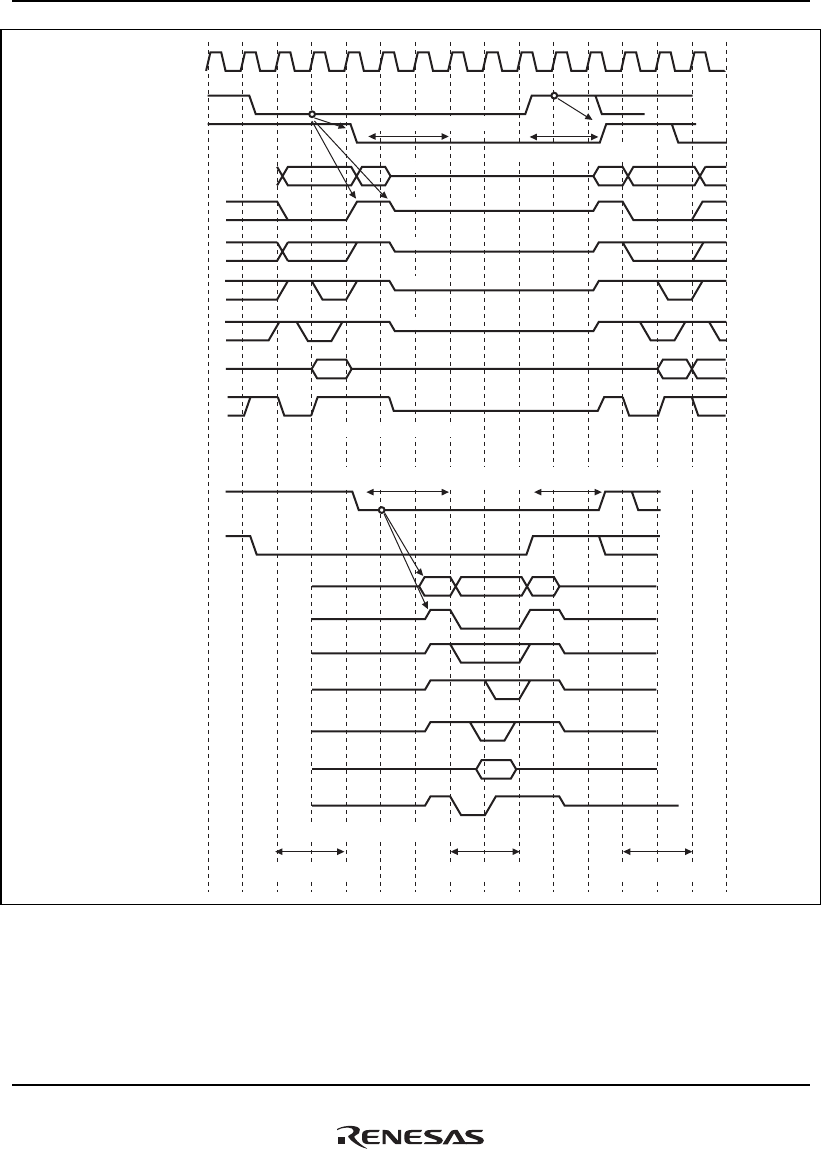
11. Local Bus State Controller (LBSC)
Rev.1.00 Jan. 10, 2008 Page 449 of 1658
REJ09B0261-0100
Asserted for 2 cycles or more
Master-mode device access
CLKOUT
BREQ
BACK
A25 to A0
CSn
R/W
RD
WEn
D31 to D0
(write)
BREQ
BACK
BS
A25 to A0
CSn
R/W
RD
WEn
BS
D31 to D0
(write)
Hi-Z
Hi-Z
Hi-Z
Hi-Z
Hi-Z
Hi-Z
Hi-Z
Hi-Z
Hi-Z Hi-Z
Hi-Z
Hi-Z
Hi-Z
Hi-Z
Negated within 2 cycles
Must be asserted
for 2 cycles or more
Must be negated
within 2 cycles
Slave-mode device access
Master access Slave access Master access
Hi-Z
Hi-Z
Hi-Z
Hi-Z
Hi-Z
Hi-Z
Hi-Z
Figure 11.42 Arbitration Sequence

11. Local Bus State Controller (LBSC)
Rev.1.00 Jan. 10, 2008 Page 450 of 1658
REJ09B0261-0100
11.5.10 Master Mode
The processor in master mode holds the bus itself until it receives a bus request.
On receiving an assertion (low level) of the bus request signal (BREQ) from the outside, the
master mode processor releases the bus and asserts (drives low) the bus use permission signal
(BACK) as soon as the currently executing bus cycle ends. On receiving the BREQ negation (high
level) indicating that the slave has released the bus, the processor negates (drives high) the BACK
signal and resumes use of the bus.
When the bus is released, all bus control output signals and input/output signals related to bus
interface enters a high-impedance state, except for BACK for bus arbitration and DACK0 to
DACK3 for controlling DMA transfer.
The actual bus release sequence is as follows.
First, the bus use permission signal is asserted in synchronization with the rising edge of the clock.
The address bus and data bus are put in a high-impedance state in synchronous with the rising
edge of the clock next to the BACK assertion. At the same time, the bus control signals (BS, CSn,
WEn, RD, R/W, CE2A, and CE2B) enters a high-impedance state. These bus control signals are
negated no later than one cycle before entering high-impedance. Bus request signal sampling is
performed on the rising edge of the clock.
The sequence for re-acquiring the bus from the slave is as follows.
As soon as BREQ negation is detected on the rising edge of the clock, BACK is negated and bus
control signal driving is started. Driving of the address bus and data bus starts at the next rising
edge of an in-phase clock. The bus control signals are asserted and the bus cycle is actually
started, at the earliest, at the clock rising edge at which the address and data signals are driven.
In order to reacquire the bus and start execution of bus access, the BREQ signal must be negated
for at least two cycles.

11. Local Bus State Controller (LBSC)
Rev.1.00 Jan. 10, 2008 Page 451 of 1658
REJ09B0261-0100
11.5.11 Slave Mode
In slave mode, usually, the bus is released. Unless the bus control is hold by performing bus
arbitration, the external device cannot be accessed. The bus is released at a reset, and the bus
arbitration sequence starts from the fetch of the reset vector.
To get the bus mastership, the BSREQ signal is asserted (driven low) in synchronous with the
rising edge of the clock. The BSACK signal, a bus use permission signal, is sampled at the rising
edge of the clock. When the asserted BSACK is detected, the bus control signal is driven low at
negate level after two cycles. At the following rising edge of the clock, the bus cycle starts. The
signal negated last at the end of the access cycle is synchronized with the rising edge of the clock.
As soon as the bus cycle ends, the BSREQ signal is negated to notify the master that the bus is
released. At the next rising edge of the clock, the control signal is put in high-impedance.
If the processor in slave mode starts access, two or more cycles of BSACK signal assertion are
required.
11.5.12 Cooperation between Master and Slave
To control system resources without contradiction by the master and slave, their respective roles
must be clearly defined, as well as in the standby state implementing power-down mode.
The design of the SH7785 provides for all control, including initialization, and standby control, to
be carried out by the master mode device.
If the SH7785 is specified as the master at a power-on reset, it will not accept bus requests from
the slave until the BREQ enable bit (BREQEN in BCR) is set to 1.
To ensure that the slave processor does not access memory requiring initialization before
completion of initialization, write 1 to the BREQ enable bit after the initialization is complete.
11.5.13 Power-Down Mode and Bus Arbitration
When deep sleep mode is used, in the system that performs bus arbitration, the BREQEN bit in
BCR of the processor in master mode should be cleared to 0 before a transition is made to deep
sleep mode. If a transition is made to deep sleep mode when the bit is set to 1, the operation is not
guaranteed.

11. Local Bus State Controller (LBSC)
Rev.1.00 Jan. 10, 2008 Page 452 of 1658
REJ09B0261-0100
11.5.14 Mode Pin Settings and General Input Output Port Settings about Data Bus Width
Table 11.18 shows the examples of MODE pin settings and port settings (GPIO port control
register) related to the selection of the data bus width used in the local bus.
Table 11.18 MODE Pin Settings and Port Settings Related to Data Bus Width Selection
GPIO Port Control Register
Data Bus
Width Data Pins MODE12 MODE11 PACR PBCR PCCR PDCR PFCR PGCR
64 bits D63 to D0 H L H'0000 H'0000 H'0000 H'0000 H'0000 H'0000
32 bits D31 to D0 Any Any Any Any Any Any H'0000 H'0000
16 bits D16 to D0 Any Any Any Any Any Any
8 bits D7 to D0 Any Any Any Any Any Any
Legend:
L: Low level
H: High level
Note: Concerning "any", setting should be correspondent to the system.
11.5.15 Pins Multiplexed with Other Modules Functions
Some pins used by the LBSC are multiplexed with general input output port (GPIO) and functions
used in other peripheral modules. The pins to be used by the LBSC should start access after setting
these pins to the LBSC functions with GPIO register. For example, when PCMCIA interface is
used, the functions of CE2A and CE2B should be enabled with the GPIO bit in PIMSELR and the
GPIO bit in PLCR before starting access.
11.5.16 Register Settings for Divided-Up DACKn Output
When the access size of DMAC1 transfer related to the local bus space is larger than the data bus
width, multiple bus cycles are generated. When multiple bus cycles are generated and CS is
negated between bus cycles, DACKn output is divided up, in the same way as CS.
Tables 11.19 to 11.22 shows the register settings when DACKn output is not divided up in DMA1
transfer and when it is divided up.

11. Local Bus State Controller (LBSC)
Rev.1.00 Jan. 10, 2008 Page 453 of 1658
REJ09B0261-0100
Table 11.19 Register Settings for Divided-Up DACKn Output in DMA1 Transfer Using the
SRAM/Burst ROM/Byte Control SRAM Interfaces
Not Divided Divided
Bus Width
[Bit]
Access Size in
DMA Transfer
Bus Cycle
Number
IWRRD, IWRRS, or
IWW in CSnBCR
ADS and ADH in
CSnWCR.
ADS and ADH
inCSnWCR
Byte 1 ⎯ ⎯ Undividable
Word 2 ⎯ B'000 B'111 to B'001
Longword 4 ⎯ B'000 B'111 to B'001
16 bytes 16 B'000 B'000 B'111 to B'001
8
32 bytes 32 ⎯ B'000 B'111 to B'001
Byte 1 ⎯ ⎯ Undividable
Word 1 ⎯ ⎯ Undividable
Longword 2 ⎯ B'000 B'111 to B'001
16 bytes 8 B'000 B'000 B'111 to B'001
16
32 bytes 16 ⎯ B'000 B'111 to B'001
Byte 1 ⎯ ⎯ Undividable
Word 1 ⎯ ⎯ Undividable
Longword 1 ⎯ ⎯ Undividable
16 bytes 4 B'000 B'000 B'111 to B'001
32
32 bytes 8 ⎯ B'000 B'111 to B'001
64 Byte 1 ⎯ ⎯ Undividable
Word 1 ⎯ ⎯ Undividable
Longword 1 ⎯ ⎯ Undividable
16 bytes 4 B'000 B'000 B'111 to B'001
32 bytes 4 ⎯ B'000 B'111 to B'001
Note: "⎯" means an arbitrary setting value. When transfer is done in a single bus cycle, DACKn
is not divided up because DACKn is output once in DMA1 transfer.

11. Local Bus State Controller (LBSC)
Rev.1.00 Jan. 10, 2008 Page 454 of 1658
REJ09B0261-0100
Table 11.20 Register Settings for Divided-Up DACKn Output in DMA1 Transfer Using the
PCMCIA Interface
Not Divided Divided
Bus Width
[Bit] Access Size Bus Cycle Number
IWRRD, IWRRS, or
IWW in CSnBCR
IWRRD, IWRRS, or
IWW in CSnBCR
Byte 1 ⎯ Undividable
Word 2 ⎯ Undividable∗1
Longword 4 ⎯ Undividable∗1
16 bytes 16 B'000 B'111 to B'001∗2
8
32 bytes 32 ⎯ Undividable∗1
16 Byte 1 ⎯ Undividable
Word 1 ⎯ Undividable
Longword 2 ⎯ Undividable∗1
16 bytes 8 B'000 B'111 to B'001∗2
32 bytes 16 ⎯ Undividable∗1
Notes: "⎯" means an arbitrary setting value. When transfer is done in a single bus cycle, DACKn
is not divided up because DACKn is output once in DMA1 transfer.
1. Multiple bus cycles are generated, however, DACKn cannot be divided.
2. Can be divided only in longword units.

11. Local Bus State Controller (LBSC)
Rev.1.00 Jan. 10, 2008 Page 455 of 1658
REJ09B0261-0100
Table 11.21 Register Settings for Divided-Up DACKn Output in DMA1 Transfer in Read
Access Using the MPX Interface
Not Divided Divided
Bus Width
[Bit] Access Size Bus Cycle Number
IWRRD or IWRRS, in
CSnBCR
IWRRD or IWRRS, in
CSnBCR
Byte 1 ⎯ Undividable
Word 1 ⎯ Undividable
Longword 1 ⎯ Undividable
16 bytes 4 Must be divided ⎯
32
32 bytes 1 ⎯ Undividable
64 Byte 1 ⎯ Undividable
Word 1 ⎯ Undividable
Longword 1 ⎯ Undividable
16 bytes 4 Must be divided ⎯
32 bytes 1 ⎯ Undividable
Note: "⎯" means an arbitrary setting value. When transfer is done in a single bus cycle, DACKn
is not divided up because DACKn is output once in DMA1 transfer.

11. Local Bus State Controller (LBSC)
Rev.1.00 Jan. 10, 2008 Page 456 of 1658
REJ09B0261-0100
Table 11.22 Register Settings for Divided-Up DACKn Output in DMA1 Transfer in Write
Access Using the MPX Interface
Not Divided Divided
Bus Width
[Bit] Access Size
Bus Cycle
Number IWW in CSnBCR
IW1 and IW0 in
CSnWCR IWW in CSnBCR
Byte 1 ⎯ ⎯ Undividable
Word 1 ⎯ ⎯ Undividable
Longword 1 ⎯ ⎯ Undividable
16 bytes 4 B'000 B'11 to B'01 B'111 to B'001
32
32 bytes 1 ⎯ ⎯ Undividable
64 Byte 1 ⎯ ⎯ Undividable
Word 1 ⎯ ⎯ Undividable
Longword 1 ⎯ ⎯ Undividable
16 bytes 4 B'000 B'11 to B'01 B'111 to B'001
32 bytes 1 ⎯ ⎯ Undividable
Note: "⎯" means an arbitrary setting value. When transfer is done in a single bus cycle, DACKn
is not divided up because DACKn is output once in DMA1 transfer.

12. DDR2-SDRAM Interface (DBSC2)
Rev.1.00 Jan. 10, 2008 Page 457 of 1658
REJ09B0261-0100
Section 12 DDR2-SDRAM Interface (DBSC2)
The DDR2-SDRAM interface (DBSC2) controls the DDR2-SDRAM.
12.1 Features
• Supports 32-bit and 16-bit external data bus widths
• Supports from DDR2-600 (controller operation at 300 MHz) to DDR2-400 (controller
operation at 200 MHz)
• Connects to 64-bit SuperHyway internal bus
• Supports 1:1 clock ratio between SuperHyway clock and DDR clock
• Queue provided for interface with SuperHyway
• During power-on reset, pin MODE8 can be used to switch between big- and little-endian
• Supports 4-bank and 8-bank DDR2-SDRAMs
• Supports sequential mode with burst length 4
• Supports Additive Latency (AL) of 0 only
• Supports differential data strobe signal (DQS, DQS)
Note: RDQS is not supported.
• Supports self-refresh
• Supports power supply backup mode
• Supported DDR2-SDRAM addresses × bit widths (total capacity) are as follows.
For details, refer to tables 12.12 through 12.19.
(When using 8-bank products, please refer to section 12.5.8, Important Information Regarding
Use of 8-Bank DDR2-SDRAM Products.)
⎯ DDR2-SDRAM data bus width: 32 bits
• Two 256 Mbits (16M × 16 bits) connected in parallel (total capacity = 512 Mbits)
• Four 256 Mbits (32M × 8 bits) connected in parallel (total capacity = 1 Gbit)
• Two 512 Mbits (32M × 16 bits) connected in parallel (total capacity = 1 Gbit)
• Four 512 Mbits (64M × 8 bits) connected in parallel (total capacity = 2 Gbits)
• Two 1 Gbit (64M × 16 bits) connected in parallel (total capacity = 2 Gbits)
• Four 1 Gbit (128M × 8 bits) connected in parallel (total capacity = 4 Gbits)
• Two 2 Gbits (128M × 16 bits) connected in parallel (total capacity = 4 Gbits)
• Four 2 Gbits (256M × 8 bits) connected in parallel (total capacity = 8 Gbits)

12. DDR2-SDRAM Interface (DBSC2)
Rev.1.00 Jan. 10, 2008 Page 458 of 1658
REJ09B0261-0100
⎯ DDR2-SDRAM data bus width: 16 bits
• One 256 Mbits (16M × 16 bits) connected in parallel (total capacity = 256 Mbits)
• Two 256 Mbits (32M × 8 bits) connected in parallel (total capacity = 512 Mbits)
• One 512 Mbits (32M × 16 bits) connected in parallel (total capacity = 512 Mbits)
• Two 512 Mbits (64M × 8 bits) connected in parallel (total capacity = 1 Gbit)
• One 1 Gbit (64M × 16 bits) connected in parallel (total capacity = 1 Gbit)
• Two 1 Gbit (128M × 8 bits) connected in parallel (total capacity = 2 Gbits)
• One 2 Gbits (128M × 16 bits) connected in parallel (total capacity = 2 Gbits)
• Two 2 Gbits (256M × 8 bits) connected in parallel (total capacity = 4 Gbits)
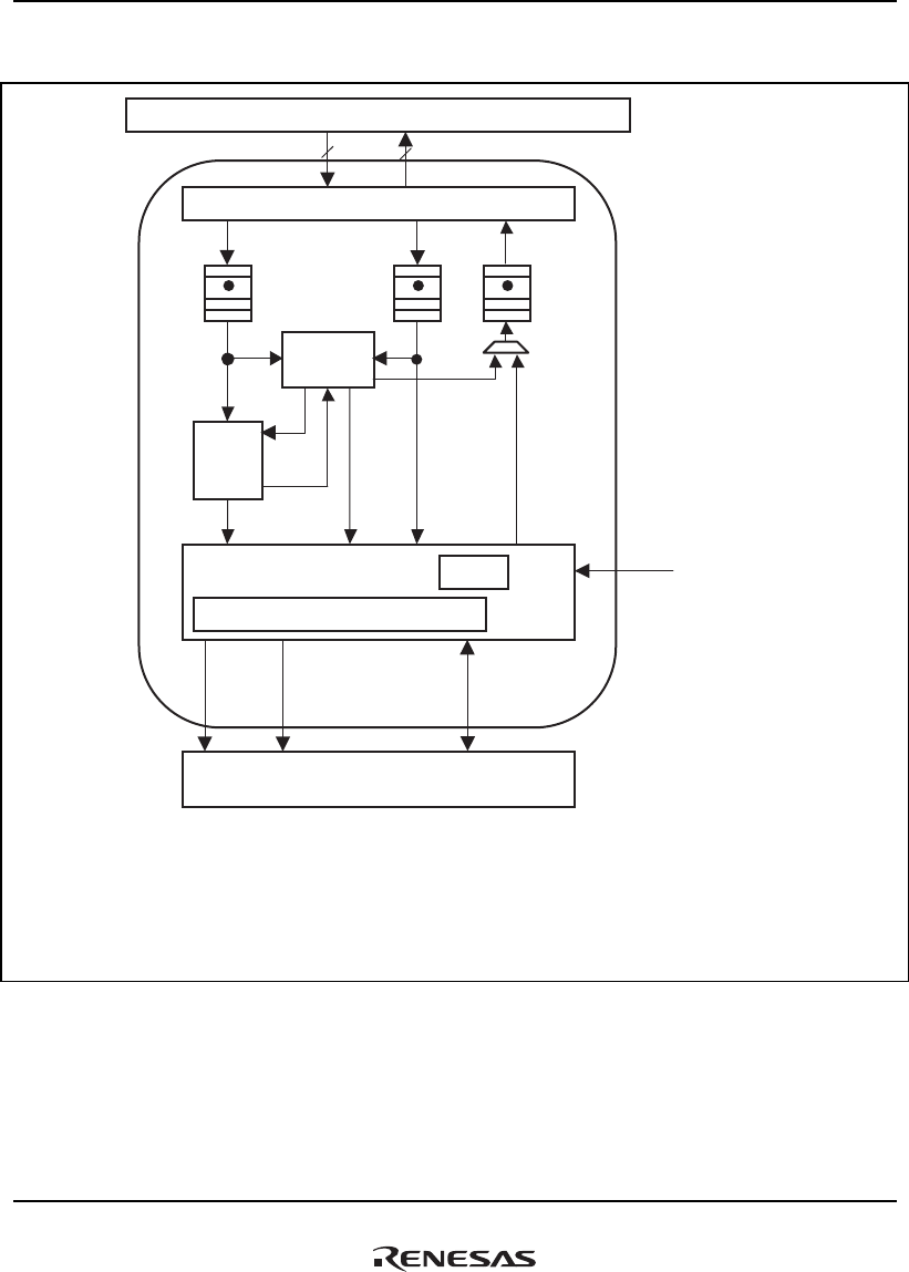
12. DDR2-SDRAM Interface (DBSC2)
Rev.1.00 Jan. 10, 2008 Page 459 of 1658
REJ09B0261-0100
Figure 12.1 shows a block diagram of the DBSC2.
BUS IF
Request
queue
Control
unit
Registers
DDRPAD DLL
IO cells
MDQS3 to MDQS0,
MDQS3 to MDQS0,
MDM3 to MDM0,
MDQ31 to MDQ0
MCKE, MA14 to MA0,
MBA2 to MBA0, MCS,
MRAS, MCAS, MWE,
MODT
Write data
queue
Response
queue
SuperHyway Bus
DDR2-SDRAM
DBSC2
MCK0/
MCK0,
MCK1/
MCK1
MBKPRST, MVREF
Notes:
Request queue:
Write data queue:
Response queue:
Control unit:
Registers:
DDRPAD:
Stores the access request of the SuperHyway bus.
Stores the write data sent from the SuperHyway bus.
Stores the read data to be sent back to the SuperHyway bus.
Controls each block depending on the request sent from the request queue.
Store timing parameters and SDRAM configuration information.
Interfaces with the DDR2-SDRAM. This incorporates the DLL
to perform phase adjustment of the DQS.
Figure 12.1 Block Diagram of the DBSC2

12. DDR2-SDRAM Interface (DBSC2)
Rev.1.00 Jan. 10, 2008 Page 460 of 1658
REJ09B0261-0100
12.2 Input/Output Pins
Table 12.1 shows the pin configuration of the DBSC2.
Table 12.1 Pin Configuration of the DBSC2
Pin Name Function I/O Description
MCK0 DDR2-SDRAM clock 0 Output Clock output for the DDR2-SDRAM
MCK0 DDR2-SDRAM clock 0 Output Clock output for the DDR2-SDRAM or
MCK0 inverted clock output
MCK1 DDR2-SDRAM clock 1 Output Clock output for the DDR2-SDRAM
MCK1 DDR2-SDRAM clock 1 Output Clock output for the DDR2-SDRAM or
MCK1 inverted clock output
MCKE Clock enable Output CKE output signal
MCS Chip select Output Chip select output signal
MWE Write enable Output Write enable output signal
MRAS Row address strobe Output Row address strobe output signal
MCAS Column address strobe Output Column address strobe output signal
MA14 to MA0 Addresses Output Address output signals
MBA2, MBA1,
MBA0
Bank active Output Bank address output signal
MDQ31 to
MDQ0
Data I/O Data I/O signals
MDQS3 to
MDQS0
I/O data strobe I/O Data strobe I/O signals
MDQS3 to
MDQS0
I/O data strobe I/O Data strobe I/O signals or MDQS3 to
MDQS0 inverted signals
MDM3 to
MDM0
Data mask Output Data mask output signals
MODT ODT enable Output ODT enable output signal to the SDRAM
MBKPRST Power backup reset Input Used in power backup mode.
When this pin is brought low level, the
MCKE pin is also pulled low.
MVREF Reference voltage input Input Input reference voltage

12. DDR2-SDRAM Interface (DBSC2)
Rev.1.00 Jan. 10, 2008 Page 461 of 1658
REJ09B0261-0100
The frequency of the SDRAM operation clocks MCK0, MCK0, MCK1, and MCK1 is the same as
the frequency of the DDR clock.
MDQ7 to MDQ0 correspond to MDQS0 and MDM0, MDQ15 to MDQ8 correspond to MDQS1
and MDM1, MDQ23 to MDQ16 correspond to MDQS2 and MDM2, and MDQ31 to MDQ24
correspond to MDQS3 and MDM3. When the external data bus width is 16 bits, MDQ15 to
MDQ0 are used.
Table 12.2 shows an example of connections when a total of four 2-Gb DDR2-SDRAM units
(256M × 8 bits) are used, with the external data bus width set to 32 bits. Command-related signals
(MCKE, MWE, MCS, MRAS, MCAS, MA14- MA0, MBA2- MBA0) are connected in common
to four DDR2-SDRAM units. Data signals (MDQ31 to MDQ0, MDQS3 to MDQS0, MDQS3 to
MDQS0, and MDM3 to MDM0) are connected to memory in 8-bit units. Clocks MCK1 and
MCK1 are connected to DDR2-SDRAM corresponding to the data signal upper sides (MDQ31 to
MDQ16, MDQS3, MDQS2, MDQS3, MDQS2, MDM3, and MDM2), and MCK0 and MCK0 are
connected to DDR2-SDRAM corresponding to the lower sides (MDQ15 to MDQ0, MDQS1,
MDQS0, MDQS1, MDQS0, MDM1, and MDM0). Address pins MA14 to MA0 should be
connected to the DDR2-SDRAM address pins, without swapping the order.
Nothing should be connected to unused pins.

12. DDR2-SDRAM Interface (DBSC2)
Rev.1.00 Jan. 10, 2008 Page 462 of 1658
REJ09B0261-0100
Table 12.2 An Example of DDR2-SDRAM Connection
(When Four 2-Gb DDR2-SDRAM Units (256 M × 8 Bits) Are Used)
Memory
MCK1,
MCK1
MCK0,
MCK0
MODT,
MCKE,
MCS,
MRAS,
MCAS,
MWE, MA14
to MA0,
MBA2 to
MBA0
MDQ31 to
MDQ24,
MDQS3,
MDQS3,
MDM3
MDQ23 to
MDQ16,
MDQS2,
MDQS2,
MDM2
MDQ15 to
MDQ8,
MDQS1,
MDQS1,
MDM1
MDQ7 to
MDQ0,
MDQS0,
MDQS0,
MDM0
Memory #1 Connected*1 Connected*2Connected*3
Memory #2 Connected*1 Connected*2 Connected*4
Memory #3 Connected*1 Connected*2 Connected*5
Memory #4 Connected*1 Connected*2 Connected*6
Notes: 1. SDRAM pins should be connected as shown below.
Memory #1 and #2
Pins SH7785 Pins
Memory #3 and #4
Pins SH7785 Pins
CK MCK1 CK MCK0
CK MCK1 CK MCK0
2. SDRAM pins should be connected as shown below.
Memory #1 to #4
Pins SH7785 Pins
Memory #1 to #4
Pins SH7785 Pins
ODT MODT A8 MA8
CKE MCKE A7 MA7
CS MCS A6 MA6
RAS MRAS A5 MA5
CAS MCAS A4 MA4
WE MWE A3 MA3
A14 MA14 A2 MA2
A13 MA13 A1 MA1
A12 MA12 A0 MA0
A11 MA11 BA2 MBA2
A10 MA10 BA1 MBA1
A9 MA9 BA0 MBA0

12. DDR2-SDRAM Interface (DBSC2)
Rev.1.00 Jan. 10, 2008 Page 463 of 1658
REJ09B0261-0100
3. SDRAM pins should be connected as shown below.
Memory #1 Pins SH7785 Pins
DQS MDQS3
DQS MDQS3
DM MDM3
DQ7 MDQ31
DQ6 MDQ30
DQ5 MDQ29
DQ4 MDQ28
DQ3 MDQ27
DQ2 MDQ26
DQ1 MDQ25
DQ0 MDQ24
4. SDRAM pins should be connected as shown below.
Memory #2 Pins SH7785 Pins
DQS MDQS2
DQS MDQS2
DM MDM2
DQ7 MDQ23
DQ6 MDQ22
DQ5 MDQ21
DQ4 MDQ20
DQ3 MDQ19
DQ2 MDQ18
DQ1 MDQ17
DQ0 MDQ16

12. DDR2-SDRAM Interface (DBSC2)
Rev.1.00 Jan. 10, 2008 Page 464 of 1658
REJ09B0261-0100
5. SDRAM pins should be connected as shown below.
Memory #3 Pins SH7785 Pins
DQS MDQS1
DQS MDQS1
DM MDM1
DQ7 MDQ15
DQ6 MDQ14
DQ5 MDQ13
DQ4 MDQ12
DQ3 MDQ11
DQ2 MDQ10
DQ1 MDQ9
DQ0 MDQ8
6. SDRAM pins should be connected as shown below.
Memory #4 Pins SH7785 Pins
DQS MDQS0
DQS MDQS0
DM MDM0
DQ7 MDQ7
DQ6 MDQ6
DQ5 MDQ5
DQ4 MDQ4
DQ3 MDQ3
DQ2 MDQ2
DQ1 MDQ1
DQ0 MDQ0

12. DDR2-SDRAM Interface (DBSC2)
Rev.1.00 Jan. 10, 2008 Page 465 of 1658
REJ09B0261-0100
12.3 Data Alignment
The DBSC2 accesses DDR2-SDRAM with a fixed burst length of 4 (figure 12.2). As shown in
table 12.3 and table 12.4, invalid read data is discarded during reading, and data mask signals are
used to mask invalid data during writing, according to the access size. The access times in tables
12.3 and 12.4 correspond to the burst times during reading/writing shown in figure 12.2. For
example, when the external bus width is 32 bits with a little endian, the second access (falling
edge of DQS) includes valid data if a byte access of address (8n + 0, 1, 2, 3) occurs.
Tables 12.5 to 12.8 show the correspondence with data on the external data bus for each access
size. During 16-byte and 32-byte accesses, quad word (8 bytes) access is combined, and the
SDRAM command is issued the necessary number of times according to the size to access the
SDRAM as shown in figures 12.3 and 12.4. The DDR2-SDRAM specification stipulates
sequential address changes (0→1→2→3, 1→2→3→0, 2→3→0→1, 3→0→1→2), so that the
address provided as a command is different for reading and for writing. Endian switching is
performed at power-on reset by switching using external pin MODE8.
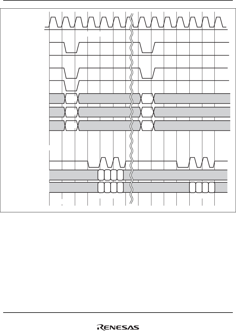
12. DDR2-SDRAM Interface (DBSC2)
Rev.1.00 Jan. 10, 2008 Page 466 of 1658
REJ09B0261-0100
MCK0,
MCK1
MA[14:11]
MA[9:0]
MBA[2:0]
MCKE
MCS
MRAS
MCAS
MWE
MA[10]
Invalid
32-bit width: MDQS[3:0]
16-bit width: MDQS[1:0]
32-bit width: MDQ[31:0]
16-bit width: MDQ[15:0]
32-bit width: MDM[3:0]
16-bit width: MDM[1:0]
Invalid
Invalid
Invalid
Invalid
READ
bank A
Invalid
Invalid
Invalid
SDRAM
command
Invalid
Invalid
Invalid
Invalid
Invalid Invalid
WRITE
bank A
Write data Read data
Valid
Valid
Valid
Valid
Valid
Valid
Example of CL = 3
High level
1
st
2
nd
3
rd
4
th
1
st
2
nd
3
rd
4
th
Figure 12.2 Burst Access Operation

12. DDR2-SDRAM Interface (DBSC2)
Rev.1.00 Jan. 10, 2008 Page 467 of 1658
REJ09B0261-0100
Table 12.3 Positions of Valid Data for Access with Burst Length of 4, when the External
Data Bus Width Is Set to 32 Bits
(1) Little Endian First Access Second Access Third Access Fourth Access
Byte access
(address 8n +
0,1,2,3)
Invalid Valid Invalid Invalid
Byte access
(address 8n +
4,5,6,7)
Valid Invalid Invalid Invalid
Word access
(address 8n + 0,2)
Invalid Valid Invalid Invalid
Word access
(address 8n + 4,6)
Valid Invalid Invalid Invalid
Longword access
(address 8n + 0)
Invalid Valid Invalid Invalid
Longword access
(address 8n + 4)
Valid Invalid Invalid Invalid
Quadword access
(address 8n + 0)
Valid Valid Invalid Invalid
(2) Big Endian First Access Second Access Third Access Fourth Access
Byte access
(address 8n +
0,1,2,3)
Valid Invalid Invalid Invalid
Byte access
(address 8n +
4,5,6,7)
Invalid Valid Invalid Invalid
Word access
(address 8n + 0,2)
Valid Invalid Invalid Invalid
Word access
(address 8n + 4,6)
Invalid Valid Invalid Invalid
Longword access
(address 8n + 0)
Valid Invalid Invalid Invalid
Longword access
(address 8n + 4)
Invalid Valid Invalid Invalid
Quadword access
(address 8n + 0)
Valid Valid Invalid Invalid

12. DDR2-SDRAM Interface (DBSC2)
Rev.1.00 Jan. 10, 2008 Page 468 of 1658
REJ09B0261-0100
Table 12.4 Positions of Valid Data for Access with Burst Length of 4, when the External
Data Bus Width Is Set to 16 Bits
(1) Little Endian First Access Second Access Third Access Fourth Access
Byte access
(address 8n + 0,1)
Invalid Invalid Invalid Valid
Byte access
(address 8n + 2,3)
Invalid Invalid Valid Invalid
Byte access
(address 8n + 4,5)
Invalid Valid Invalid Invalid
Byte access
(address 8n + 6,7)
Valid Invalid Invalid Invalid
Word access
(address 8n + 0)
Invalid Invalid Invalid Valid
Word access
(address 8n + 2)
Invalid Invalid Valid Invalid
Word access
(address 8n + 4)
Invalid Valid Invalid Invalid
Word access
(address 8n + 6)
Valid Invalid Invalid Invalid
Longword access
(address 8n + 0)
Invalid Invalid Valid Valid
Longword access
(address 8n + 4)
Valid Valid Invalid Invalid
Quadword access
(address 8n + 0)
Valid Valid Valid Valid

12. DDR2-SDRAM Interface (DBSC2)
Rev.1.00 Jan. 10, 2008 Page 469 of 1658
REJ09B0261-0100
(2) Big Endian First Access Second Access Third Access Fourth Access
Byte access
(address 8n + 0,1)
Valid Invalid Invalid Invalid
Byte access
(address 8n + 2,3)
Invalid Valid Invalid Invalid
Byte access
(address 8n + 4,5)
Invalid Invalid Valid Invalid
Byte access
(address 8n + 6,7)
Invalid Invalid Invalid Valid
Word access
(address 8n + 0)
Valid Invalid Invalid Invalid
Word access
(address 8n + 2)
Invalid Valid Invalid Invalid
Word access
(address 8n + 4)
Invalid Invalid Valid Invalid
Word access
(address 8n + 6)
Invalid Invalid Invalid Valid
Longword access
(address 8n + 0)
Valid Valid Invalid Invalid
Longword access
(address 8n + 4)
Invalid Invalid Valid Valid
Quadword access
(address 8n + 0)
Valid Valid Valid Valid

12. DDR2-SDRAM Interface (DBSC2)
Rev.1.00 Jan. 10, 2008 Page 470 of 1658
REJ09B0261-0100
Table 12.5 Data Alignment for Access in Little Endian when External Data Bus Width Is
Set to 32 Bits
Access Size Address
MDQ31 to
MDQ24
MDQ23 to
MDQ16
MDQ15 to
MDQ8
MDQ7 to
MDQ0
Address 0 Data
7 to 0
Address 1 Data
7 to 0
Address 2 Data
7 to 0
Address 3 Data
7 to 0
Address 4 Data
7 to 0
Address 5 Data
7 to 0
Address 6 Data
7 to 0
Byte
Address 7 Data
7 to 0
Address 0 Data
15 to 8
Data
7 to 0
Address 2 Data
15 to 8
Data
7 to 0
Address 4 Data
15 to 8
Data
7 to 0
Word
Address 6 Data
15 to 8
Data
7 to 0
Longword Address 0 Data
31 to 24
Data
23 to 16
Data
15 to 8
Data
7 to 0
Address 4 Data
31 to 24
Data
23 to 16
Data
15 to 8
Data
7 to 0

12. DDR2-SDRAM Interface (DBSC2)
Rev.1.00 Jan. 10, 2008 Page 471 of 1658
REJ09B0261-0100
Access Size Address
MDQ31 to
MDQ24
MDQ23 to
MDQ16
MDQ15 to
MDQ8
MDQ7 to
MDQ0
Quadword Address 0
(First access:
address 4)
Data
63 to 56
Data
55 to 48
Data
47 to 40
Data
39 to 32
Address 0
(Second access:
Address 0)
Data
31 to 24
Data
23 to 16
Data
15 to 8
Data
7 to 0
Table 12.6 Data Alignment for Access in Big Endian when External Data Bus Width Is Set
to 32 Bits
Access Size Address
MDQ31 to
MDQ24
MDQ23 to
MDQ16
MDQ15 to
MDQ8
MDQ7 to
MDQ0
Byte Address 0 Data
7 to 0
Address 1 Data
7 to 0
Address 2 Data
7 to 0
Address 3 Data
7 to 0
Address 4 Data
7 to 0
Address 5 Data
7 to 0
Address 6 Data
7 to 0
Address 7 Data
7 to 0

12. DDR2-SDRAM Interface (DBSC2)
Rev.1.00 Jan. 10, 2008 Page 472 of 1658
REJ09B0261-0100
Access Size Address
MDQ31 to
MDQ24
MDQ23 to
MDQ16
MDQ15 to
MDQ8
MDQ7 to
MDQ0
Word Address 0 Data
15 to 8
Data
7 to 0
Address 2 Data
15 to 8
Data
7 to 0
Address 4 Data
15 to 8
Data
7 to 0
Address 6 Data
15 to 8
Data
7 to 0
Longword Address 0 Data
31 to 24
Data
23 to 16
Data
15 to 8
Data
7 to 0
Address 4 Data
31 to 24
Data
23 to 16
Data
15 to 8
Data
7 to 0
Quadword Address 0
(First access:
Address 0)
Data
63 to 56
Data
55 to 48
Data
47 to 40
Data
39 to 32
Address 0
(Second access:
Address 4)
Data
31 to 24
Data
23 to 16
Data
15 to 8
Data
7 to 0

12. DDR2-SDRAM Interface (DBSC2)
Rev.1.00 Jan. 10, 2008 Page 473 of 1658
REJ09B0261-0100
Table 12.7 Data Alignment for Access in Little Endian when External Data Bus Width Is
Set to 16 Bits
Access Size Address MDQ15 to MDQ8 MDQ7 to MDQ0
Byte Address 0 Data
7 to 0
Address 1 Data
7 to 0
Address 2 Data
7 to 0
Address 3 Data
7 to 0
Address 4 Data
7 to 0
Address 5 Data
7 to 0
Address 6 Data
7 to 0
Address 7 Data
7 to 0
Word Address 0 Data
15 to 8
Data
7 to 0
Address 2 Data
15 to 8
Data
7 to 0
Address 4 Data
15 to 8
Data
7 to 0
Address 6 Data
15 to 8
Data
7 to 0

12. DDR2-SDRAM Interface (DBSC2)
Rev.1.00 Jan. 10, 2008 Page 474 of 1658
REJ09B0261-0100
Access Size Address MDQ15 to MDQ8 MDQ7 to MDQ0
Longword Address 0
(First access:
Address 2)
Data
31 to 24
Data
23 to 16
Address 0
(Second access:
Address 0)
Data
15 to 8
Data
7 to 0
Address 4
(First access:
Address 6)
Data
31 to 24
Data
23 to 16
Address 4
(Second access:
Address 4)
Data
15 to 8
Data
7 to 0
Quadword Address 0
(First access:
Address 6)
Data
63 to 56
Data
55 to 48
Address 0
(Second access:
Address 4)
Data
47 to 40
Data
39 to 32
Address 0
(Third access:
Address 2)
Data
31 to 24
Data
23 to 16
Address 0
(Fourth access:
Address 0)
Data
15 to 8
Data
7 to 0

12. DDR2-SDRAM Interface (DBSC2)
Rev.1.00 Jan. 10, 2008 Page 475 of 1658
REJ09B0261-0100
Table 12.8 Data Alignment for Access in Big Endian when External Data Bus Width Is Set
to 16 Bits
Access Size Address MDQ15 to MDQ8 MDQ7 to MDQ0
Byte Address 0 Data
7 to 0
Address 1 Data
7 to 0
Address 2 Data
7 to 0
Address 3 Data
7 to 0
Address 4 Data
7 to 0
Address 5 Data
7 to 0
Address 6 Data
7 to 0
Address 7 Data
7 to 0
Word Address 0 Data
15 to 8
Data
7 to 0
Address 2 Data
15 to 8
Data
7 to 0
Address 4 Data
15 to 8
Data
7 to 0
Address 6 Data
15 to 8
Data
7 to 0

12. DDR2-SDRAM Interface (DBSC2)
Rev.1.00 Jan. 10, 2008 Page 476 of 1658
REJ09B0261-0100
Access Size Address MDQ15 to MDQ8 MDQ7 to MDQ0
Longword Address 0
(First access:
Address 0)
Data
31 to 24
Data
23 to 16
Address 0
(Second access:
Address 2)
Data
15 to 8
Data
7 to 0
Address 4
(First access:
Address 4)
Data
31 to 24
Data
23 to 16
Address 4
(Second access:
Address 6)
Data
15 to 8
Data
7 to 0
Quadword Address 0
(First access:
Address 0)
Data
63 to 56
Data
55 to 48
Address 0
(Second access:
Address 2)
Data
47 to 40
Data
39 to 32
Address 0
(Third access:
Address 4)
Data
31 to 24
Data
23 to 16
Address 0
(Fourth access:
Address 6)
Data
15 to 8
Data
7 to 0

12. DDR2-SDRAM Interface (DBSC2)
Rev.1.00 Jan. 10, 2008 Page 477 of 1658
REJ09B0261-0100
When the external bus width is set to 16 bits
Address 16n + 0
Address 16n + 8
1st access 2nd access
16n + 0 16n + 8
16n + 8 16n + 0
16-byte read/write access (a total of two commands are issued)
Address 32n + 0
Address 32n + 8
Address 32n + 16
Address 32n + 24
1st access 2nd access 3rd access 4th access
32n + 0 32n + 8 32n + 16 32n + 24
32-byte read access (a total of four commands are issued)
32n + 0 32n + 8 32n + 16 32n+ 24
32n + 16 32n + 24 32n + 0 32n + 8
32n + 16 32n + 24 32n + 0 32n + 8
Address 32n + 0
Address 32n + 8
Address 32n + 16
Address 32n + 24
1st access 2nd access 3rd access 4th access
32n + 0 32n + 8 32n + 16 32n + 24
32-byte write access (a total of four commands are issued)
32n + 0 32n + 8 32n + 16 32n + 24
32n + 16 32n + 24 32n + 0 32n + 8
32n + 16 32n + 24 32n + 0 32n + 8
Figure 12.3 Addresses Generated upon 16/32-Byte Access when the External Data Bus
Width Is 16 Bits

12. DDR2-SDRAM Interface (DBSC2)
Rev.1.00 Jan. 10, 2008 Page 478 of 1658
REJ09B0261-0100
When the external bus width is set to 32 bits
Address 16n + 0
Address 16n + 8
1st access
16-byte read/write access (a total of one command is issued)
1st access 2nd access
32-byte read access (a total of two commands are issued)
1st access 2nd access
32-byte write access (a total of two commands are issued)
Address 32n + 0
Address 32n + 8
Address 32n + 16
Address 32n + 24
Address 32n + 0
Address 32n + 8
Address 32n + 16
Address 32n + 24
16n + 0
16n + 8
32n + 0 32n + 16
32n + 0 32n + 16
32n + 16 32n + 0
32n + 16 32n + 0
32n + 0 32n + 16
32n + 0 32n + 16
32n + 16 32n + 0
32n + 16 32n + 0
Figure 12.4 Addresses Generated upon 16/32-Byte Access when the External Data Bus
Width Is 32 Bits

12. DDR2-SDRAM Interface (DBSC2)
Rev.1.00 Jan. 10, 2008 Page 479 of 1658
REJ09B0261-0100
12.4 Register Descriptions
Table 12.9 shows the DBSC2 register configuration; Table 12.10 shows register states in the
different processing modes.
The register bit width is 32 bits, and the longword size (32 bits) should be used for register access.
If registers are accessed with sizes other than the longword size, correct operation cannot be
guaranteed.
The DBSC2 register area is, in P4 addresses, from H'FE80 0000 to H'FEFF FFFF and in area 7
addresses, from H'FE800000 to H'FEFFFFFA. If an address other than the register addresses
indicated in table 12.9 is accessed, correct operation cannot be guaranteed.

12. DDR2-SDRAM Interface (DBSC2)
Rev.1.00 Jan. 10, 2008 Page 480 of 1658
REJ09B0261-0100
Table 12.9 DBSC2 Register Configuration
Register Name Abbreviation R/W P4 Area Address Area 7 Address
Access
Size
(Bits)
Synchroni-
zation
Clock
DBSC2 status
register
DBSTATE R H'FE80 000C H'1E80 000C 32 DDRck
SDRAM
operation enable
register
DBEN R/W H'FE80 0010 H'1E80 0010 32 DDRck
SDRAM
command
control register
DBCMDCNT R/W H'FE80 0014 H'1E80 0014 32 DDRck
SDRAM
configuration
setting register
DBCONF R/W H'FE80 0020 H'1E80 0020 32 DDRck
SDRAM timing
register 0
DBTR0 R/W H'FE80 0030 H'1E80 0030 32 DDRck
SDRAM timing
register 1
DBTR1 R/W H'FE80 0034 H'1E80 0034 32 DDRck
SDRAM timing
register 2
DBTR2 R/W H'FE80 0038 H'1E80 0038 32 DDRck
SDRAM refresh
control register 0
DBRFCNT0 R/W H'FE80 0040 H'1E80 0040 32 DDRck
SDRAM refresh
control register 1
DBRFCNT1 R/W H'FE80 0044 H'1E80 0044 32 DDRck
SDRAM refresh
control register 2
DBRFCNT2 R/W H'FE80 0048 H'1E80 0048 32 DDRck
SDRAM refresh
status register
DBRFSTS R/W H'FE80 004C H'1E80 004C 32 DDRck
DDRPAD
frequency
setting register
DBFREQ R/W H'FE80 0050 H'1E80 0050 32 DDRck
DDRPAD DIC,
ODT, OCD
setting register
DBDICODTO
CD
R/W H'FE80 0054 H'1E80 0054 32 DDRck
SDRAM mode
setting register
DBMRCNT W H'FE80 0060 H'1E80 0060 32 DDRck

12. DDR2-SDRAM Interface (DBSC2)
Rev.1.00 Jan. 10, 2008 Page 481 of 1658
REJ09B0261-0100
Table 12.10 Register Status in each Processing Mode
Power-On Reset Manual Reset Sleep/Deep Sleep
Register Name Abbreviation
By PRESET pin/
WDT/H-UDI
By WDT/Multiple
Exception
By SLEEP
Instruction
DBSC2 status
register
DBSTATE H'0000 0x00* Retained Retained
SDRAM operation
enable register
DBEN H'0000 0000 Retained Retained
SDRAM command
control register
DBCMDCNT H'0000 0000 Retained Retained
SDRAM
configuration
setting register
DBCONF H'009A 0001 Retained Retained
SDRAM timing
register 0
DBTR0 H'0203 0501 Retained Retained
SDRAM timing
register 1
DBTR1 H'0001 0001 Retained Retained
SDRAM timing
register 2
DBTR2 H'0104 0303 Retained Retained
SDRAM refresh
control register 0
DBRFCNT0 H'0000 0000 Retained Retained
SDRAM refresh
control register 1
DBRFCNT1 H'0000 0200 Retained Retained
SDRAM refresh
control register 2
DBRFCNT2 H'1000 0080 Retained Retained
SDRAM refresh
status register
DBRFSTS H'0000 0000 Retained Retained
DDRPAD
frequency setting
register
DBFREQ H'0000 0000 Retained Retained
DDRPAD DIC,
ODT, OCD setting
register
DBDICODTOCD H'0000 0007 Retained Retained
SDRAM mode
setting register
DBMRCNT Undefined Retained Retained
Note: * Initial value is specified by external pin MODE8.

12. DDR2-SDRAM Interface (DBSC2)
Rev.1.00 Jan. 10, 2008 Page 482 of 1658
REJ09B0261-0100
12.4.1 DBSC2 Status Register (DBSTATE)
The DBSC2 status register (DBSTATE) is a read-only register. Writing is invalid. It is initialized
only upon power-on reset.
161718192021222324252627282931 30
0000000000000000
⎯⎯⎯⎯⎯⎯⎯⎯⎯⎯⎯⎯⎯⎯⎯⎯
RRRRRRRRRRRRRRRR
BIt:
Initial value:
R/W:
01234567891011121315 14
00000000x*0000000
⎯⎯⎯⎯⎯⎯⎯⎯ENDN⎯⎯⎯⎯⎯⎯⎯
RRRRRRRRRRRRRRRR
BIt:
Initial value:
R/W:
Note: * Initial value is specified by external pin MODE8.
Bit Bit Name
Initial
Value R/W Description
31 to 9 ⎯ All 0 R Reserved
These bits are always read as 0.
8 ENDN ×* R Endian Display Bit
Displays the endian of the DBSC2 set by external pin
MODE8.
0: Big endian
1: Little endian
7 to 0 ⎯ All 0 R Reserved
These bits are always read as 0.
Note: * Initial value is specified by external pin MODE8.

12. DDR2-SDRAM Interface (DBSC2)
Rev.1.00 Jan. 10, 2008 Page 483 of 1658
REJ09B0261-0100
12.4.2 SDRAM Operation Enable Register (DBEN)
The SDRAM operation enable register (DBEN) is a readable/writable register. It is initialized only
upon power-on reset.
161718192021222324252627282931 30
0000000000000000
⎯⎯⎯⎯⎯⎯⎯⎯⎯⎯⎯⎯⎯⎯⎯⎯
RRRRRRRRRRRRRRRR
BIt:
Initial value:
R/W:
01234567891011121315 14
0000000000000000
ACEN⎯⎯⎯⎯⎯⎯⎯⎯⎯⎯⎯⎯⎯⎯⎯
R/WRRRRRRRRRRRRRRR
BIt:
Initial value:
R/W:
Bit Bit Name
Initial
Value R/W Description
31 to 1 ⎯ All 0 R Reserved
These bits are always read as 0. The write value should
always be 0.
Operation when a value other than 0 is written is not
guaranteed.
0 ACEN 0 R/W SDRAM Access Enable Bit
By setting this bit, data accessing of SDRAM is enabled.
When set to 0, access is disabled; when set to 1,
access is enabled. When access is disabled, attempts
to access SDRAM are ignored. This bit is used for the
initialization sequence or self-refresh operation.
0: Disables access
1: Enables access

12. DDR2-SDRAM Interface (DBSC2)
Rev.1.00 Jan. 10, 2008 Page 484 of 1658
REJ09B0261-0100
12.4.3 SDRAM Command Control Register (DBCMDCNT)
The SDRAM command control register (DBCMDCNT) is a readable/writable register. It is
initialized only upon power-on reset. The CMD2 to CMD0 bits in DBCMDCNT are always read
as 000.
161718192021222324252627282931 30
0000000000000000
⎯⎯⎯⎯⎯⎯⎯⎯⎯⎯⎯⎯⎯⎯⎯⎯
RRRRRRRRRRRRRRRR
BIt:
Initial value:
R/W:
01234567891011121315 14
0000000000000000
CMD0CMD1CMD2⎯⎯⎯⎯⎯⎯⎯⎯⎯⎯⎯⎯⎯
R/WR/WR/WRRRRRRRRRRRRR
BIt:
Initial value:
R/W:
Bit Bit Name
Initial
Value R/W Description
31 to 3 ⎯ All 0 R Reserved
These bits are always read as 0. The write value should
always be 0.
Operation when a value other than 0 is written is not
guaranteed.

12. DDR2-SDRAM Interface (DBSC2)
Rev.1.00 Jan. 10, 2008 Page 485 of 1658
REJ09B0261-0100
Bit Bit Name
Initial
Value R/W Description
2 to 0 CMD2 to
CMD0
000 R/W SDRAM Command Issue Bit
These bits are used to issue commands necessary to
execute the DDR2-SDRAM initialization sequence and
self-refresh transition/cancellation. When these bits are
written, the command corresponding to the written value
is issued once. For example, in order to issue the auto-
refresh command twice, it would be necessary to write
100 to these bits twice. The precharge interval,
minimum interval between auto-refresh and the next
command, and other intervals are values set in the
SDRAM timing register, described below. When read,
these bits are always read as 000.
Once writing is performed to enable the MCKE signal, it
remains enabled. During self-refresh control, the MCKE
goes to low level, but on cancellation MCKE
automatically returns to high level.
For details on the MCKE signal operation, refer to
section 12.5.13, Regarding MCKE Signal Operation.
000: Normal operation (power-on reset)
001: Setting prohibited (Correct operation cannot be
guaranteed.)
010: Precharge (PALL) command issued
011: The MCKE signal is enabled (high level).
100: Auto-refresh (REF) command issued
101 to 111: Setting prohibited (Correct operation cannot
be guaranteed.)
Note: This register can be written only when automatic issue of auto-refresh is disabled (the
ARFEN bit in the DBRFCNT0 register is cleared to 0).

12. DDR2-SDRAM Interface (DBSC2)
Rev.1.00 Jan. 10, 2008 Page 486 of 1658
REJ09B0261-0100
12.4.4 SDRAM Configuration Setting Register (DBCONF)
The SDRAM configuration setting register (DBCONF) is a readable/writable register. It is
initialized only upon power-on reset.
161718192021222324252627282931 30
0101100100000000
SPILT0SPILT1SPILT2SPILT3SPILT4SPILT5SPILT6SPILT7
⎯⎯⎯⎯⎯⎯⎯⎯
R/WR/WR/WR/WR/WR/WR/WR/WRRRRRRRR
BIt:
Initial value:
R/W:
01234567891011121315 14
1000000000000000
BWID
TH0
BWID
TH1
⎯⎯⎯⎯⎯⎯
BASFT0BASFT1
⎯⎯⎯⎯⎯⎯
R/WR/WRRRRRRR/WR/WRRRRRR
BIt:
Initial value:
R/W:
Bit Bit Name
Initial
Value R/W Description
31 to 24 ⎯ All 0 R Reserved
These bits are always read as 0. The write value should
always be 0.
Operation when a value other than 0 is written is not
guaranteed.
23 to 16 SPLIT7 to
SPLIT0
1001 1010 R/W Memory Configuration Select Bits
These bits select the memory configuration to be used.
These are used in combination with the BASFT and the
BWIDTH bits. For details on address multiplexing, refer
to section 12.5.6, Regarding Address Multiplexing.
1001 1010: 256-Mbit product (16M × 16 bits)
1001 1011: 512-Mbit product (32M × 16 bits)
1101 1011: 1-Gbit product (64M × 16 bits)
1110 0011: 2-Gbit product (128M × 16 bits)
0001 1011: 256-Mbit product (32M × 8 bits)
0010 0011: 512-Mbit product (64M × 8 bits)
0110 0011: 1-Gbit product (128M × 8 bits)
0110 1011: 2-Gbit product (256M × 8 bits)
Other than above: Setting prohibited (If specified,
correct operation cannot be
guaranteed.)

12. DDR2-SDRAM Interface (DBSC2)
Rev.1.00 Jan. 10, 2008 Page 487 of 1658
REJ09B0261-0100
Bit Bit Name
Initial
Value R/W Description
15 to 10 ⎯ All 0 R Reserved
These bits are always read as 0. The write value should
always be 0.
Operation when a value other than 0 is written is not
guaranteed.
9, 8 BASFT1
and
BASFT0
00 R/W Bank Address Shift Bits
These bits select the amount of shifting downward of
the bank address.
00: No shift
01: Shift the bank address downward 1 bit.
10: Shift the bank address downward 2 bits.
11: Shift the bank address downward 3 bits.
7 to 3 ⎯ All 0 R Reserved
These bits are always read as 0. The write value should
always be 0.
Operation when a value other than 0 is written is not
guaranteed.
1, 0 BWIDTH1
and
BWIDTH0
01 R/W SDRAM Bus Width Setting Bits
These bits set the external data bus width.
00: Setting prohibited (If specified, correct operation
cannot be guaranteed.)
01: 16 bits
10: 32 bits
11: Setting prohibited (If specified, correct operation
cannot be guaranteed.)
Note: Writing to this register should be performed only when the following conditions are met.
• When SDRAM access is disabled (when the ACEN bit in the DBEN register is 0.).
• When automatic issue of auto-refresh is disabled (when the ARFEN bit in the
DBRFCNT0 register is cleared to 0.).

12. DDR2-SDRAM Interface (DBSC2)
Rev.1.00 Jan. 10, 2008 Page 488 of 1658
REJ09B0261-0100
12.4.5 SDRAM Timing Register 0 (DBTR0)
The SDRAM timing register 0 (DBTR0) is a readable/writable register. It is initialized only upon
power-on reset.
161718192021222324252627282931 30
1100000001000000
TRAS0TRAS1TRAS2TRAS3
⎯⎯⎯⎯
CL0CL1CL2
⎯⎯⎯⎯⎯
R/WR/WR/WR/WRRRRR/WR/WR/WRRRRR
BIt:
Initial value:
R/W:
01234567891011121315 14
1000000010100000
TRCD0TRCD1TRCD2
⎯⎯⎯⎯⎯
TRFC0TRFC1TRFC2TRFC3TRFC4TRFC5
⎯
TRFC6
R/WR/WR/WRRRRRR/WR/WR/WR/WR/WR/WR R/W
BIt:
Initial value:
R/W:
Bit Bit Name
Initial
Value R/W Description
31 to 27 ⎯ All 0 R Reserved
These bits are always read as 0. The write value should
always be 0.
Operation when a value other than 0 is written is not
guaranteed.
26 to 24 CL2 to CL0 010 R/W CAS Latency Setting Bits
These bits set the CAS latency. These bits should be
set according to the DDR2-SDRAM specifications. The
number of cycles is the number of DDR clock cycles.
When using the ODT (On Die Termination) enable
output signal MODT, these bits should be set to 4 or
more cycles.
000: Setting prohibit (If specified, correct operation
cannot be guaranteed.)
001: Setting prohibit (If specified, correct operation
cannot be guaranteed.)
010: 2 cycles
011: 3 cycles
100: 4 cycles
101: 5 cycles
110: 6 cycles
111: Setting prohibit (If specified, correct operation
cannot be guaranteed.)

12. DDR2-SDRAM Interface (DBSC2)
Rev.1.00 Jan. 10, 2008 Page 489 of 1658
REJ09B0261-0100
Bit Bit Name
Initial
Value R/W Description
23 to 20 ⎯ All 0 R Reserved
These bits are always read as 0. The write value should
always be 0.
Operation when a value other than 0 is written is not
guaranteed.
19 to 16 TRAS3 to
TRAS0
0011 R/W tRAS (ACT-PRE period) Setting Bits
These bits set the ACT-PRE minimum period constraint
for the same bank. These bits should be set according
to the DDR2-SDRAM specifications. The number of
cycles is the number of DDR clock cycles.
0000: Setting prohibit (If specified, correct operation
cannot be guaranteed.)
:
0010: Setting prohibit (If specified, correct operation
cannot be guaranteed.)
0011: 4 cycles
0100: 5 cycles
:
1110: 15 cycles
1111: Setting prohibit (If specified, correct operation
cannot be guaranteed.)
15 ⎯ 0 R Reserved
This bit is always read as 0. The write value should
always be 0.
Operation when a value other than 0 is written is not
guaranteed.

12. DDR2-SDRAM Interface (DBSC2)
Rev.1.00 Jan. 10, 2008 Page 490 of 1658
REJ09B0261-0100
Bit Bit Name
Initial
Value R/W Description
14 to 8 TRFC6 to
TRFC0
000 0101 R/W tRFC (REF-ACT/REF period) Setting Bits
These bits set the REF-ACT/REF minimum period
constraint These bits should be set according to the
DDR2-SDRAM specifications. The number of cycles is
the number of DDR clock cycles.
000 0000: Setting prohibit (If specified, correct operation
cannot be guaranteed.)
:
000 0100: Setting prohibit (If specified, correct operation
cannot be guaranteed.)
000 0101: 6 cycles
000 0110: 7 cycles
:
100 0001: 66 cycles
100 0010: Setting prohibit (If specified, correct operation
cannot be guaranteed.)
:
111 1111: Setting prohibit (If specified, correct operation
cannot be guaranteed.)
7 to 3 ⎯ All 0 R Reserved
These bits are always read as 0. The write value should
always be 0.
Operation when a value other than 0 is written is not
guaranteed.

12. DDR2-SDRAM Interface (DBSC2)
Rev.1.00 Jan. 10, 2008 Page 491 of 1658
REJ09B0261-0100
Bit Bit Name
Initial
Value R/W Description
2 to 0 TRCD2 to
TRCD0
001 R/W tRCD (ACT-READ/WRITE period) Setting Bits
These bits set the ACT-READ/WRITE minimum period.
These bits should be set according to the DDR2-
SDRAM specifications. The number of cycles is the
number of DDR clock cycles.
000: Setting prohibit (If specified, correct operation
cannot be guaranteed.)
001: 2 cycles
010: 3 cycles
011: 4 cycles
100: 5 cycles
101: Setting prohibit (If specified, correct operation
cannot be guaranteed.)
:
111: Setting prohibit (If specified, correct operation
cannot be guaranteed.)
Notes: 1. AL (Additive Latency) supported by the DBSC2 is only 0.
2. Writing to this register should be performed only when the following conditions are met.
• When SDRAM access is disabled (when the ACEN bit in the DBEN register is 0.).
• When automatic issue of auto-refresh is disabled (when the ARFEN bit in the
DBRFCNT0 register is cleared to 0.).

12. DDR2-SDRAM Interface (DBSC2)
Rev.1.00 Jan. 10, 2008 Page 492 of 1658
REJ09B0261-0100
12.4.6 SDRAM Timing Register 1 (DBTR1)
The SDRAM timing register 1 (DBTR1) is a readable/writable register. It is initialized only upon
power-on reset.
161718192021222324252627282931 30
1000000000000000
TRP0TRP1TRP2
⎯⎯⎯⎯⎯⎯⎯⎯⎯⎯⎯⎯⎯
R/WR/WR/WRRRRRRRRRRRRR
BIt:
Initial value:
R/W:
01234567891011121315 14
1000000000000000
TWR0TWR1TWR2
⎯⎯⎯⎯⎯
TRRD0TRRD1TRRD2
⎯⎯⎯⎯⎯
R/WR/WR/WRRRRRR/WR/WR/WRRRRR
BIt:
Initial value:
R/W:
Bit Bit Name
Initial
Value R/W Description
31 to 19 ⎯ All 0 R Reserved
These bits are always read as 0. The write value should
always be 0.
Operation when a value other than 0 is written is not
guaranteed.
18 to 16 TRP2 to
TRP0
001 R/W tRP (PRE-ACT/REF period) Setting Bits
These bits set the PRE-ACT minimum period constraint
for the same bank. These bits should be set according
to the DDR2-SDRAM specifications. The number of
cycles is the number of DDR clock cycles.
000: Setting prohibit (If specified, correct operation
cannot be guaranteed.)
001: 2 cycles
010: 3 cycles
011: 4 cycles
100: 5 cycles
101: Setting prohibit (If specified, correct operation
cannot be guaranteed.)
:
111: Setting prohibit (If specified, correct operation
cannot be guaranteed.)

12. DDR2-SDRAM Interface (DBSC2)
Rev.1.00 Jan. 10, 2008 Page 493 of 1658
REJ09B0261-0100
Bit Bit Name
Initial
Value R/W Description
15 to 11 ⎯ All 0 R Reserved
These bits are always read as 0. The write value should
always be 0.
Operation when a value other than 0 is written is not
guaranteed.
10 to 8 TRRD2 to
TRRD0
000 R/W tRRD (ACT(A)-ACT(B) period) Setting Bits
These bits set the ACT-ACT minimum period constraint
for the different banks. These bits should be set
according to the DDR2-SDRAM specifications. The
number of cycles is the number of DDR clock cycles.
000: 1 cycle
001: 2 cycles
010: 3 cycles
011: 4 cycles
100: Setting prohibit (If specified, correct operation
cannot be guaranteed.)
:
111: Setting prohibit (If specified, correct operation
cannot be guaranteed.)
7 to 3 ⎯ All 0 R Reserved
These bits are always read as 0. The write value should
always be 0.
Operation when a value other than 0 is written is not
guaranteed.

12. DDR2-SDRAM Interface (DBSC2)
Rev.1.00 Jan. 10, 2008 Page 494 of 1658
REJ09B0261-0100
Bit Bit Name
Initial
Value R/W Description
2 to 0 TWR2 to
TWR0
001 R/W tWR (write recovery period) Setting Bits
These bits set the write recovery minimum period
constraint. These bits should be set according to the
DDR2-SDRAM specifications. The number of cycles is
the number of DDR clock cycles.
000: Setting prohibit (If specified, correct operation
cannot be guaranteed.)
001: 2 cycles
010: 3 cycles
011: 4 cycles
100: 5 cycles
101: Setting prohibit (If specified, correct operation
cannot be guaranteed.)
:
111: Setting prohibit (If specified, correct operation
cannot be guaranteed.)
Note: Writing to this register should be performed only when the following conditions are met.
• When SDRAM access is disabled (when the ACEN bit in the DBEN register is 0.).
• When automatic issue of auto-refresh is disabled (when the ARFEN bit in the
DBRFCNT0 register is cleared to 0.).

12. DDR2-SDRAM Interface (DBSC2)
Rev.1.00 Jan. 10, 2008 Page 495 of 1658
REJ09B0261-0100
12.4.7 SDRAM Timing Register 2 (DBTR2)
The SDRAM timing register 2 (DBTR2) is a readable/writable register. It is initialized only upon
power-on reset.
161718192021222324252627282931 30
0010000010000000
TRC0TRC1TRC2TRC3TRC4
⎯⎯⎯
TRTP0TRTP1
⎯⎯⎯⎯⎯⎯
R/WR/WR/WR/WR/WRRRR/WR/WRRRRRR
BIt:
Initial value:
R/W:
01234567891011121315 14
1100000011000000
WRRD0WRRD1WRRD2WRRD3
⎯⎯⎯⎯
RDWR0RDWR1RDWR2RDWR3
⎯⎯⎯⎯
R/WR/WR/WR/WRRRRR/WR/WR/WR/WRRRR
BIt:
Initial value:
R/W:
Bit Bit Name
Initial
Value R/W Description
31 to 26 ⎯ All 0 R Reserved
These bits are always read as 0. The write value should
always be 0.
Operation when a value other than 0 is written is not
guaranteed.
25, 24 TRTP1 and
TRTP0
01 R/W tRTP (READ-PRE command minimum time) Setting Bits
These bits set the READ-PRE command minimum time
constraint for the same bank. These bits should be set
according to the SDRAM specifications. The number of
cycles is the number of DDR clock cycles.
00: Setting prohibit (If specified, correct operation
cannot be guaranteed.)
01: 2 cycles
10: 3 cycles
11: Setting prohibit (If specified, correct operation
cannot be guaranteed.)
23 to 21 ⎯ All 0 R Reserved
These bits are always read as 0. The write value should
always be 0.
Operation when a value other than 0 is written is not
guaranteed.

12. DDR2-SDRAM Interface (DBSC2)
Rev.1.00 Jan. 10, 2008 Page 496 of 1658
REJ09B0261-0100
Bit Bit Name
Initial
Value R/W Description
20 to 16 TRC4 to
TRC0
0 0100 R/W tRC (ACT-ACT/REF period) Setting Bits
These bits set the constraint for the minimum time from
ACT command to ACT command (in the same bank)/
REF command. These bits should be set according to
the SDRAM specifications. The number of cycles is the
number of DDR clock cycles.
00000: Setting prohibit (If specified, correct operation
cannot be guaranteed.)
:
00011: Setting prohibit (If specified, correct operation
cannot be guaranteed.)
00100: 5 cycles
00101: 6 cycles
:
10010: 19 cycles
10011: Setting prohibit (If specified, correct operation
cannot be guaranteed.)
:
11111: Setting prohibit (If specified, correct operation
cannot be guaranteed.)
15 to 12 ⎯ All 0 R Reserved
These bits are always read as 0. The write value should
always be 0.
Operation when a value other than 0 is written is not
guaranteed.

12. DDR2-SDRAM Interface (DBSC2)
Rev.1.00 Jan. 10, 2008 Page 497 of 1658
REJ09B0261-0100
Bit Bit Name
Initial
Value R/W Description
11 to 8 RDWR3 to
RDWR0
0011 R/W READ-WRITE Command Minimum Interval Setting Bits
These bits set the READ-WRITE command minimum
interval constraint. These bits should be set according
to the SDRAM specifications. The number of cycles is
the number of DDR clock cycles.
0000: Setting prohibit (If specified, correct operation
cannot be guaranteed.)
:
0010: Setting prohibit (If specified, correct operation
cannot be guaranteed.)
0011: 4 cycles
0100: 5 cycles
:
1000: 9 cycles
1001: Setting prohibit (If specified, correct operation
cannot be guaranteed.)
:
1111: Setting prohibit (If specified, correct operation
cannot be guaranteed.)
7 to 4 ⎯ All 0 R Reserved
These bits are always read as 0. The write value should
always be 0.
Operation when a value other than 0 is written is not
guaranteed.

12. DDR2-SDRAM Interface (DBSC2)
Rev.1.00 Jan. 10, 2008 Page 498 of 1658
REJ09B0261-0100
Bit Bit Name
Initial
Value R/W Description
3 to 0 WRRD3 to
WRRD0
0011 R/W WRITE-READ Command Minimum Interval Setting Bits
These bits set the WRITE-READ command minimum
interval constraint. These bits should be set according
to the SDRAM specifications. The number of cycles is
the number of DDR clock cycles.
0000: Setting prohibit (If specified, correct operation
cannot be guaranteed.)
:
0010: Setting prohibit (If specified, correct operation
cannot be guaranteed.)
0011: 4 cycles
0100: 5 cycles
:
1010: 11 cycles
1011: Setting prohibit (If specified, correct operation
cannot be guaranteed.)
:
1111: Setting prohibit (If specified, correct operation
cannot be guaranteed.)
Note: Writing to this register should be performed only when the following conditions are met.
• When SDRAM access is disabled (when the ACEN bit in the DBEN register is 0.).
• When automatic issue of auto-refresh is disabled (when the ARFEN bit in the
DBRFCNT0 register is cleared to 0.).

12. DDR2-SDRAM Interface (DBSC2)
Rev.1.00 Jan. 10, 2008 Page 499 of 1658
REJ09B0261-0100
12.4.8 SDRAM Refresh Control Register 0 (DBRFCNT0)
The SDRAM refresh control register 0 (DBRFCNT0) is a readable/writable register. It is
initialized only upon power-on reset.
161718192021222324252627282931 30
0000000000000000
ARFEN
⎯⎯⎯⎯⎯⎯⎯⎯⎯⎯⎯⎯⎯⎯⎯
R/WRRRRRRRRRRRRRRR
BIt:
Initial value:
R/W:
01234567891011121315 14
0000000000000000
SRFEN
⎯⎯⎯⎯⎯⎯⎯⎯⎯⎯⎯⎯⎯⎯⎯
R/WRRRRRRRRRRRRRRR
BIt:
Initial value:
R/W:
Bit Bit Name
Initial
Value R/W Description
31 to 17 ⎯ All 0 R Reserved
These bits are always read as 0. The write value should
always be 0.
Operation when a value other than 0 is written is not
guaranteed.
16 ARFEN 0 R/W Auto-Refresh Enable Bit
Enables or disables automatic issue of auto-refresh.
The auto-refresh command is issued periodically
according to the settings of DBRFCNT1/2.
For details on the auto-refresh command issue timing,
refer to section 12.5.5, Auto-Refresh Operation.
0: Disables automatic issue of auto-refresh.
1: Enables automatic issue of auto-refresh.
15 to 1 ⎯ All 0 R Reserved
These bits are always read as 0. The write value should
always be 0.
Operation when a value other than 0 is written is not
guaranteed.

12. DDR2-SDRAM Interface (DBSC2)
Rev.1.00 Jan. 10, 2008 Page 500 of 1658
REJ09B0261-0100
Bit Bit Name
Initial
Value R/W Description
0 SRFEN 0 R/W Self-Refresh Mode Bit
Performs transition to or cancellation of self-refresh
mode. By writing 1, a transition is made to self-refresh.
By writing 0, self-refresh mode is cancelled. For details
on transition to or cancellation of self-refresh, refer to
section 12.5.4, Self-Refresh Operation.
0: Cancels self-refresh.
1: Makes a transition to self-refresh.
12.4.9 SDRAM Refresh Control Register 1 (DBRFCNT1)
The SDRAM refresh control register 1 (DBRFCNT1) is a readable/writable register. It is
initialized only upon power-on reset.
161718192021222324252627282931 30
0000000000000000
⎯⎯⎯⎯⎯⎯⎯⎯⎯⎯⎯⎯⎯⎯⎯⎯
RRRRRRRRRRRRRRRR
BIt:
Initial value:
R/W:
01234567891011121315 14
0000000001000000
TREFI0TREFI1TREFI2TREFI3TREFI4TREFI5TREFI6TREFI7TREFI8TREFI9TREFI10TREFI11TREFI12
⎯⎯⎯
R/WR/WR/WR/WR/WR/WR/WR/WR/WR/WR/WR/WR/WRRR
BIt:
Initial value:
R/W:
Bit Bit Name
Initial
Value R/W Description
31 to 13 ⎯ All 0 R Reserved
These bits are always read as 0. The write value should
always be 0.
Operation when a value other than 0 is written is not
guaranteed.

12. DDR2-SDRAM Interface (DBSC2)
Rev.1.00 Jan. 10, 2008 Page 501 of 1658
REJ09B0261-0100
Bit Bit Name
Initial
Value R/W Description
12 to 0 TREFI12 to
TREFI0
0 0010
0000 0000
R/W Average Refresh Interval Setting Bits
These bits set the average interval for auto-refresh
operation. Upon refresh execution, this value is added
to the refresh interval count register.
The number of cycles is the number of DDR clock
cycles.
0 0000 0000 0000: Setting prohibited (If specified,
correct operation cannot be
guaranteed.)
:
0 0000 0011 1111: Setting prohibited (If specified,
correct operation cannot be
guaranteed.)
0 0000 0100 0000: 65 cycles
0 0000 0100 0001: 66 cycles
:
1 1111 1111 1111: 8192 cycles
Note: Writing to this register should be performed only when the following condition is met.
• When automatic issue of auto-refresh is disabled (when the ARFEN bit in the
DBRFCNT0 register is cleared to 0.).

12. DDR2-SDRAM Interface (DBSC2)
Rev.1.00 Jan. 10, 2008 Page 502 of 1658
REJ09B0261-0100
12.4.10 SDRAM Refresh Control Register 2 (DBRFCNT2)
The SDRAM refresh control register 2 (DBRFCNT2) is a readable/writable register. It is
initialized only upon power-on reset.
161718192021222324252627282931 30
0000000000001000
LV1
TH0
LV1
TH1
LV1
TH2
LV1
TH3
LV1
TH4
LV1
TH5
LV1
TH6
LV1
TH7
LV1
TH8
LV1
TH9
LV1
TH10
LV1
TH11
LV1
TH12
LV1
TH13
⎯
LV1
TH14
R/WR/WR/WR/WR/WR/WR/WR/WR/WR/WR/WR/WR/WR/WR R/W
BIt:
Initial value:
R/W:
01234567891011121315 14
0000000100000000
LV0
TH0
LV0
TH1
LV0
TH2
LV0
TH3
LV0
TH4
LV0
TH5
LV0
TH6
LV0
TH7
⎯⎯⎯⎯⎯⎯⎯⎯
R/WR/WR/WR/WR/WR/WR/WR/WRRRRRRRR
BIt:
Initial value:
R/W:
Bit Bit Name
Initial
Value R/W Description
31 ⎯ 0 R Reserved
This bit is always read as 0. The write value should
always be 0.
Operation when a value other than 0 is written is not
guaranteed.
30 to 16 LV1TH14 to
LV1TH0
001 0000
0000 0000
R/W Level 1 Threshold Setting Bits
These bits set the threshold cycles for executing auto-
refresh when there is a vacancy in access requests
received via the SuperHyway bus.
The number of cycles is the number of DDR clock
cycles.
When the internal refresh counter value exceeds
LV1TH, and there are consecutive requests received via
the SuperHyway bus, request processing is given
priority over auto-refresh.
The relation between LV1TH and LV0TH must satisfy
the relation LV1TH ≥ LV0TH. Correct operation cannot
be guaranteed if LV1TH <LV0TH.
The value of LV1TH should be set larger than the
constraint TRAS between PRE and ACT set in the
SDRAM timing register 0. If a value equal to or less than
TRAS is set, Correct operation cannot be guaranteed.

12. DDR2-SDRAM Interface (DBSC2)
Rev.1.00 Jan. 10, 2008 Page 503 of 1658
REJ09B0261-0100
Bit Bit Name
Initial
Value R/W Description
15 to 8 ⎯ All 0 R Reserved
These bits are always read as 0. The write value should
always be 0.
Operation when a value other than 0 is written is not
guaranteed.
7 to 0 LV0TH7 to
LV0TH0
1000 0000 R/W Level 0 Threshold Setting Bits
These bits set the threshold cycles for executing auto-
refresh. The number of cycles is the number of DDR
clock cycles.
When single-unit requests received via the SuperHyway
bus end, auto refresh is given priority over the next
request.
Notes: 1. The TREFI bit value of the DBRFCNT1 register and the LV1TH bit of this register are
added and the result used as the maximum value of the auto-refresh counter, that is,
the maximum interval for refresh commands when periodically issuing auto-refresh
signals. Specify the LV1TH bit value so that the maximum interval is within the
maximum value of the ACT-PRE command interval prescribed in the datasheet of the
respective memory manufacturers. For details, refer to section 12.5.5, Auto-Refresh
Operation.
2. Writing to this register should be performed only when the following condition is met.
When automatic issue of auto-refresh is disabled (when the ARFEN bit in the
DBRFCNT0 register is cleared to 0.).

12. DDR2-SDRAM Interface (DBSC2)
Rev.1.00 Jan. 10, 2008 Page 504 of 1658
REJ09B0261-0100
12.4.11 SDRAM Refresh Status Register (DBRFSTS)
The SDRAM refresh status register (DBRFSTS) is a readable/writable register. It is initialized
only upon power-on reset.
161718192021222324252627282931 30
0000000000000000
⎯⎯⎯⎯⎯⎯⎯⎯⎯⎯⎯⎯⎯⎯⎯⎯
RRRRRRRRRRRRRRRR
BIt:
Initial value:
R/W:
01234567891011121315 14
0000000000000000
RFUDF
⎯⎯⎯⎯⎯⎯⎯⎯⎯⎯⎯⎯⎯⎯⎯
R/WRRRRRRRRRRRRRRR
BIt:
Initial value:
R/W:
Bit Bit Name
Initial
Value R/W Description
31 to 1 ⎯ All 0 R Reserved
These bits are always read as 0. The write value should
always be 0.
Operation when a value other than 0 is written is not
guaranteed.
0 RFUDF 0 R/W Refresh Counter Underflow Bit
Set to 1 to indicate that the refresh counter has
underflows when the refresh counter changes from 1 to
0. This bit is cleared to 0 by writing 0 to it.
Underflow may occur because the LV0TH bit value is
smaller than the maximum number of command
execution cycles, so that refresh cannot be issued until
the counter value reaches 0. In this case, the value of
the LV0TH bit should be changed.
For details on the refresh counter, refer to section
12.5.5, Auto-Refresh Operation.
0: Indicates that no underflow occurs.
1: Indicates that an underflow occurs.

12. DDR2-SDRAM Interface (DBSC2)
Rev.1.00 Jan. 10, 2008 Page 505 of 1658
REJ09B0261-0100
12.4.12 DDRPAD Frequency Setting Register (DBFREQ)
The DDRPAD frequency setting register (DBFREQ) is a readable/writable register. It is initialized
only upon power-on reset.
161718192021222324252627282931 30
0000000000000000
⎯⎯⎯⎯⎯⎯⎯⎯⎯⎯⎯⎯⎯⎯⎯⎯
RRRRRRRRRRRRRRRR
BIt:
Initial value:
R/W:
01234567891011121315 14
0000000000000000
FREQ0FREQ1FREQ2
⎯⎯⎯⎯⎯
DLLRST
⎯⎯⎯⎯⎯⎯⎯
R/WR/WR/WRRRRRR/WRRRRRRR
BIt:
Initial value:
R/W:
Bit Bit Name
Initial
Value R/W Description
31 to 9 ⎯ All 0 R Reserved
These bits are always read as 0. The write value should
always be 0.
Operation when a value other than 0 is written is not
guaranteed.
8 DLLRST 0 R/W DLL Reset Bit
Resets the DLL within DDRPAD. The FREQ bits should
be used to set the frequency when this bit is 0. If the
FREQ bit is changed when this bit is 1, correct
operation cannot be guaranteed.
0: Resets the frequency setting
1: Generates or retains the frequency setting
7 to 3 ⎯ All 0 R Reserved
These bits are always read as 0. The write value should
always be 0.
Operation when a value other than 0 is written is not
guaranteed.

12. DDR2-SDRAM Interface (DBSC2)
Rev.1.00 Jan. 10, 2008 Page 506 of 1658
REJ09B0261-0100
Bit Bit Name
Initial
Value R/W Description
2 to 0 FREQ2 to
FREQ0
000 R/W Frequency Setting Bits
These bits set the operating frequency of the data bus
in the DDR2-SDRAM.
000: up to 300 MHz (DDR2-600)
001: Reserved
010: 200 MHz (DDR2-400)
100 to 111: Setting prohibited. (If specified, correct
operation cannot be guaranteed.)
Note: This register is used for initialization, when canceling self-refresh, and when canceling
power supply backup.
For details, refer to section 12.5.3, Initialization Sequence, section 12.5.4, Self-Refresh
Operation, and (2) Recovery from SDRAM Power Supply Backup Mode in section 12.5.10,
DDR2-SDRAM Power Supply Backup Function.

12. DDR2-SDRAM Interface (DBSC2)
Rev.1.00 Jan. 10, 2008 Page 507 of 1658
REJ09B0261-0100
12.4.13 DDRPAD DIC, ODT, OCD Setting Register (DBDICODTOCD)
The SDRAM refresh status register (DBRFSTS) is a readable/writable register. It is initialized
only upon power-on reset.
161718192021222324252627282931 30
0000000000000000
DICDIC_CKDIC_DQDIC_AD
⎯⎯⎯⎯
DDRSIG
⎯⎯⎯⎯⎯⎯⎯
R/WR/WR/WR/WRRRRR/WRRRRRRR
BIt:
Initial value:
R/W:
01234567891011121315 14
1110000000000000
⎯⎯⎯⎯⎯⎯⎯⎯
T_ODT0T_ODT1
ODT_
EARLY
ODTEN0ODTEN1
⎯⎯⎯
R/WR/WR/WRRRRRR/WR/WR/WR/WR/WRRR
BIt:
Initial value:
R/W:
Bit Bit Name
Initial
Value R/W Description
31 to 25 ⎯ All 0 R Reserved
These bits are always read as 0. The write value should
always be 0.
Operation when a value other than 0 is written is not
guaranteed.
24 DDRSIG 0 R/W Write Preamble Time Setting Bit
Sets the preamble time of the DQS signal to be output
when data is written to the DDR2-SDRAM. The number
of cycles is the number of DDR clock cycles.
0: Write preamble time = 0.5 cycle
1: Write preamble time = 1 cycle
23 to 20 ⎯ All 0 R Reserved
These bits are always read as 0. The write value should
always be 0.
Operation when a value other than 0 is written is not
guaranteed.
19 DIC_AD 0 R/W Address and Command Pin Impedance Value
This bit should be set to the same value as the value set
for DIC of EMRS(1) in the DDR2-SDRAM.
0: Normal
1: Weak

12. DDR2-SDRAM Interface (DBSC2)
Rev.1.00 Jan. 10, 2008 Page 508 of 1658
REJ09B0261-0100
Bit Bit Name
Initial
Value R/W Description
18 DIC_DQ 0 R/W Data Pin Impedance value
This bit should be set to the same value as the value set
for DIC of EMRS(1) in the DDR2-SDRAM.
0: Normal
1: Weak
17 DIC_CK 0 R/W Clock Pin Impedance value
This bit should be set to the same value as the value set
for DIC of EMRS(1) in the DDR2-SDRAM.
0: Normal
1: Weak
16 DIC 0 R/W Impedance Value Set in the DIC of EMRS(1) in the
SDRAM
This bit should be set to the same value as the value set
for DIC of EMRS(1) in the DDR2-SDRAM.
0: Normal
1: Weak
15 to 13 ⎯ All 0 R Reserved
These bits are always read as 0. The write value should
always be 0.
If a value other than 0 is written, correct operation
cannot be guaranteed.
12, 11 ODTEN1
and
ODTEN0
00 R/W ODT Output Mode Switch
These bits switch the ODT output mode.
For details on the note when the ODTEN bits are set to
01, refer to section 12.5.9, Important Information
Regarding ODT Control Signal Output to SDRAM.
00: The ODT pin is fixed low regardless of WRITE
command issue.
01: The ODT pin is fixed high when the WRITE
command is issued.
10 and 11: The ODT pin is fixed high regardless of
WRITE command issue.

12. DDR2-SDRAM Interface (DBSC2)
Rev.1.00 Jan. 10, 2008 Page 509 of 1658
REJ09B0261-0100
Bit Bit Name
Initial
Value R/W Description
10 ODT_
EARLY
0 R/W ODT Assertion Period Setting
Sets the ODT assertion period. The number of cycles is
the number of DDR clock cycles.
This setting is valid only when ODTEN is set to 01. In
order to extend ODT by 1 cycle using the setting of
ODT_EARLY, after setting CL to 5 or higher, the RDWR
bits in the DBTR2 register must be set to the value
specified in the data sheet for the DDR2-SDRAM, plus
1.
For details on the note when the ODTEN bits are set to
01, refer to section 12.5.9, Important Information
Regarding ODT Control Signal Output to SDRAM.
0: Asserts the ODT pin to high for 3 cycles for one write
command.
1: Asserts the ODT pin to high for 4 cycles for one write
command.
9, 8 T_ODT1
and
T_ODT0
00 R/W ODT Resistance Value Setting
These bits set the resistance value of the ODT
resistance within DDRPAD turned on for DDR2-SDRAM
reading. They should be set to the same value as the
Rtt set in EMRS(1) of DDR2-SDRAM.
00: ODT disabled
01: 75 Ω
10: 150 Ω
11: Setting prohibited (If specified, correct operation
cannot be guaranteed.)
7 to 3 ⎯ All 0 R Reserved
These bits are always read as 0. The write value should
always be 0.
If a value other than 0 is written, correct operation
cannot be guaranteed.
2 to 0 ⎯ 111 R/W Reserved
These bits should always be written to 111. If these bits
are written to the value other than 111, correct operation
cannot be guaranteed.

12. DDR2-SDRAM Interface (DBSC2)
Rev.1.00 Jan. 10, 2008 Page 510 of 1658
REJ09B0261-0100
12.4.14 SDRAM Mode Setting Register (DBMRCNT)
The SDRAM mode setting register (DBMRCNT) is a write-only register. If it is read, correct
operation cannot be guaranteed.
161718192021222324252627282931 30
⎯⎯⎯⎯⎯⎯⎯⎯⎯⎯⎯⎯⎯⎯⎯⎯
BA0BA1BA2
⎯⎯⎯⎯⎯⎯⎯⎯⎯⎯⎯⎯⎯
WWWWWWWWWWWWWWWW
BIt:
Initial value:
R/W:
01234567891011121315 14
⎯⎯⎯⎯⎯⎯⎯⎯⎯⎯⎯⎯⎯⎯⎯⎯
MA0MA1MA2MA3MA4MA5MA6MA7MA8MA9MA10MA11MA12MA13
⎯
MA14
WWWWWWWWWWWWWWWW
BIt:
Initial value:
R/W:
Bit Bit Name
Initial
Value R/W Description
31 to 19 ⎯ Undefined W Reserved
These bits are always read as 0. The write value should
always be 0.
If a value other than 0 is written, correct operation
cannot be guaranteed.
18 to 16 BA2 to BA0 Undefined W SDRAM Mode Register and Extended Mode Register
Setting Bits
Bank address pins MBA2, MBA1, and MBA0
correspond to bit 18, bit 17, and bit 16, respectively.
15 ⎯ Undefined W Reserved
This bit is always read as 0. The write value should
always be 0.
If a value other than 0 is written, correct operation
cannot be guaranteed.
14 to 0 MA14 to
MA0
Undefined W SDRAM Mode Register and Extended Mode Register
Setting Bits
The address pins MA14, MA13, ..., and MA0
correspond to bit 14, bit 13, ..., and bit 0, respectively.

12. DDR2-SDRAM Interface (DBSC2)
Rev.1.00 Jan. 10, 2008 Page 511 of 1658
REJ09B0261-0100
By writing to this register, the DDR2-SDRAM address and bank address pins can be directly
manipulated to set the mode and extended mode registers. When this register is written, the mode
register setting (MRS)/extended mode register setting (EMRS) command is issued for the DDR2-
SDRAM. Upon command execution, settings should be made such that the burst length is 4, the
mode is sequential access mode, and the additive latency (AL) is 0, the DQS is enable, and the
RDQS is disable. Further, settings should be made such that the CAS latency (CL)/write recovery
(WR) is equal to the corresponding bits in SDRAM timing registers 0 and 1 (DBTR0 and
DBTR1).

12. DDR2-SDRAM Interface (DBSC2)
Rev.1.00 Jan. 10, 2008 Page 512 of 1658
REJ09B0261-0100
12.5 DBSC2 Operation
12.5.1 Supported SDRAM Commands
Table 12.11 lists the SDRAM commands issued by the DBSC2. These commands are issued to the
DDR2-SDRAM in synchronously with MCK0, MCK0, MCK1, and MCK1. In the table, n-1
indicates the state of the signal applied to DDR2-SDRAM one cycle before SDRAM command
issue; n indicates the state of the signal at the time of command issue.
Table 12.11 SDRAM Commands Issued by the DBSC2
MCKE
Function Symbol n-1 n MCS MRAS MCAS MWE
MA
[14:11]
MA10/
AP
MBA
[2:0]
MA
[9:0]
Device
deslect
DSEL H H H X X X X X X X
Read READ H H L H L H V L V V
Write WRITE H H L H L L V L V V
Bank activate ACT H H L L H H V V V V
Precharge
select bank
PRE H H L L H L X L V X
Precharge all
banks
PALL H H L L H L X H X X
Auto-
refresh
REF H H L L L H X X X X
Self-
refresh entry
from IDLE
SLFRSH H L L L L H X X X X
Self-
refresh exit
SLFRSHX L H H X X X X X X X
Mode register
set
MRS/
EMRS
H H L L L L V V V V
Legend:
H: High level
L: Low level
X: High or low level (don't care)
V: Valid data
The above DSEL command is issued when DDR2-SDRAM is not accessed, and so need not be
explicitly issued by the user.

12. DDR2-SDRAM Interface (DBSC2)
Rev.1.00 Jan. 10, 2008 Page 513 of 1658
REJ09B0261-0100
12.5.2 SDRAM Command Issue
(1) Basic Access
The DBSC2 stores in a queue the requests received via the SuperHyway bus. Request processing
is begun around the time of preceding precharge/activate processing, but processing completion is
in the order received in the queue.
When SDRAM initialization is completed, upon receiving a read/write request, a page miss occurs
with all banks in the closed state. Hence the DBSC2 first issues an activate (ACT) command, to
open the corresponding bank. After opening the bank, the read/write command of the SDRAM
corresponding to the read/write request is issued. At this time, the number of issued read/write
commands differs depending on the bus width and the request size (1/2/4/8/16/32 bytes), as
indicated in figure 12.5. For example, when performing 32-byte reading from the SuperHyway
bus with an external data bus width of 32 bytes, two read commands are executed. When issuing
the read command in the first cycle, data is read with a burst length of 4 (two DDR clock cycles),
so that it is necessary to wait until the third cycle to issue the second read command.
When access ends, the DBSC2 leaves the bank open, without using a precharge (PRE) command.
The bank is closed when (1) the following request is for the same bank with a different row
address; (2) there is an auto-refresh request; or (3) the user issues a precharge-all (PALL)
command using the SDRAM command control register, for self-refresh processing.
Thus in normal access other than self-refresh, the DBSC2 uses hardware for bank management, so
that except for the register settings upon initialization, the user need not execute control.
Further, the DBSC2 performs multi-bank operation of four banks. Hence the maximum number of
banks which can be opened simultaneously is four. Refer to section 12.5.6, Regarding Address
Multiplexing, for the correspondence between access addresses from the SuperHyway bus and
SDRAM bank/row addresses.
When using the SDRAM with a memory capacity of 1 Gbit or greater, refer to section 12.5.8,
Important Information Regarding Use of 8-Bank DDR2-SDRAM Products.
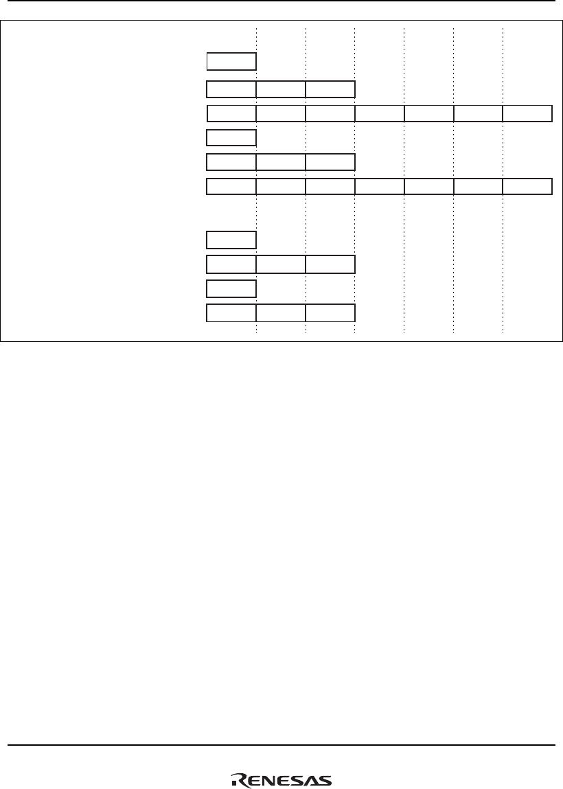
12. DDR2-SDRAM Interface (DBSC2)
Rev.1.00 Jan. 10, 2008 Page 514 of 1658
REJ09B0261-0100
16-bit external bus
Read (16 bytes)
Read (1, 2, 4, 8, or 16 bytes)
Read (32 bytes)
Write (1, 2, 4, 8, or 16 bytes)
Write (32 bytes)
Read (1, 2, 4, or 8 bytes)
Read (32 bytes)
Write (1, 2, 4, or 8 bytes)
Write (16 bytes)
Read
Write (32 bytes)
Write
Read
Read
Write
Write
Read
Read Read Read
Write
Write Write Write
DSEL
DSEL DSEL DSEL
DSEL
DSEL DSEL DSEL
Read
Read Read
DSEL
Write
Write WriteDSEL
32-bit external bus
1 command
2 commands
4 commands
1 command
2 commands
4 commands
1 command
2 commands
1 command
2 commands
1st cycle 2nd cycle 3rd cycle 4th cycle 5th cycle 6th cycle 7th cycle
Figure 12.5 Read/Write Command Issued to the SDRAM in Response
to the Request from the SuperHyway Bus
(2) Preceding Precharge/Activate Processing
In order to utilize DDR2-SDRAM multibank functions to reduce SDRAM command vacant cycles
insofar as possible and improve the efficiency of bus use, the DBSC2 issues in advance a
PRE/ACT command corresponding to the following request queue page miss processing. Only the
PRE/ACT command is issued in advance, so there is no change in the read/write order. A
PRE/ACT command is issued in advance only when the following request (1) results in a page
miss, and moreover (2) entails access of a bank different from that of the request currently being
processed. Figure 12.6 shows an example of execution of preceding precharge/activate processing.
This is an example of a command issued to the SDRAM when the external data bus width is 32
bits, the PRE/ACT minimum time constraint is 3 cycles, the ACT-READ/WRITE minimum time
constraint is 3 cycles, and the ACT (A)-ACT (B) minimum time constraint is 2 cycles. In this
example, the first through fourth requests are accumulated, and the first request is the request
initially provided to the queue.
First, at time 1 the DBSC2 issues to the SDRAM a PRE command for the first read (16-byte)
request processing. Then, when determining the command to be issued at time 2, due to timing
constraints it is not possible to issue at time 2 the ACT command necessary as request processing
for the first read (16-byte) request, which has higher priority. Hence the DBSC2 searches for a
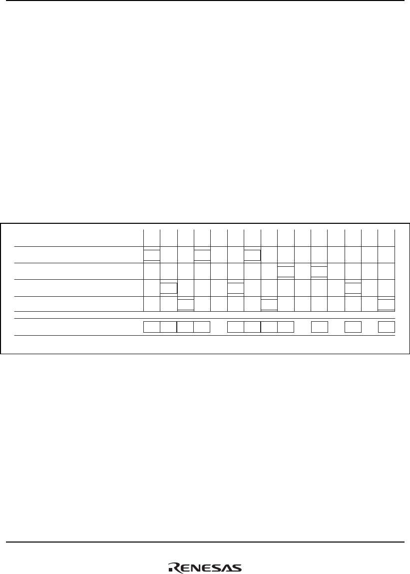
12. DDR2-SDRAM Interface (DBSC2)
Rev.1.00 Jan. 10, 2008 Page 515 of 1658
REJ09B0261-0100
command to be issued at time 2 from the following request queue. From the search results it is
seen that advance precharge processing can be executed for the third read (8-byte) request and the
fourth read (16-byte) request. Because the DBSC2 gives priority to preceding requests, it decides
to perform advance precharge processing for the third read (8-byte) request, and issues a PRE
command to the SDRAM.
When the time advances to time 3, the ACT command cannot be issued for the first read (16-byte)
request at time 3 either, and so a search of the following queue is performed for a command which
can be issued. Due to timing constraints, the ACT command cannot be issued for the third read (8-
byte) request, and as a result, issuance of the PRE command corresponding to the fourth read (16-
byte) request is selected.
At time 4, it is possible to execute request processing for the first read (16-byte) request, and an
ACT command is issued to the DDR2-SDRAM.
Thereafter, the processing described above is repeated.
Request
No.
1
2
3
4
SDRAM command
Request
Read (16 bytes)
Read (32 bytes)
Read (8 bytes)
Read (16 bytes)
Bank to be
accessed
Bank 0
Bank 1
Bank 2
Bank 3
Page state
during request
Miss
Hit
Miss
Miss
1 2 3 4 5 6 7 8 9 10 11 12 13 14 15
PRE
PRE PRE PRE ACT ACT READ ACT READ READ READREAD
PRE
PRE
ACT
ACT
READ
READ READ
READ
READ
Time Time Time Time Time Time Time Time Time Time Time Time Time Time Time
As the burst length is 4 in the DDR2-SDRAM, the interval between READ commands is always two cycles.
ACT
Figure 12.6 Example of Preceding Precharge/Activate Processing

12. DDR2-SDRAM Interface (DBSC2)
Rev.1.00 Jan. 10, 2008 Page 516 of 1658
REJ09B0261-0100
12.5.3 Initialization Sequence
The following shows an example of the initialization sequence. For detailed information such as
the power supply and timing parameters, please refer to the datasheet for the DDR2-SDRAM
being used.
1. Following the instructions in the datasheet guide for the SDRAM being used, supply the power
and the reference voltage.
2. After the power-on reset has been canceled for the LSI and the CPU has begun operating, the
system judges whether the LSI was in power supply backup mode or the normal initialization
sequence (for information on entering settings in power backup mode, please refer to (2)
Recovery from SDRAM Power Supply Backup Mode in section 12.5.10, DDR2-SDRAM
Power Supply Backup Function). If it was an initialization sequence, the software is used to
initiate a wait of at least 100 μs. (An example of how to make the system wait for a specific
interval such as 100 μs can be found in section 12.5.11, Method for Securing Time Required
for Initialization, Self-Refresh Cancellation, etc.)
3. Enter the settings for the SDRAM configuration setting register (DBCONF), the SDRAM
timing register 0 (DBTR0), the SDRAM timing register 1 (DBTR1), and the SDRAM timing
register 2 (DBTR2).
4. DLL settings are entered by writing them to the DDRPAD frequency setting register
(DBFREQ).
A. Set DLLRST = 0.
B. Set the frequency of DDRPAD in the FREQ bit.
C. After DLLRST has been set to 1, the time interval of 100 μs that the DLL needs in order to
stabilize is applied through the software. The clock stabilization supply time of 200 μs that
is required for the DDR2-SDRAM to boot, including the wait time described in item 2
above, can be assured.
5. Write the setting to the DDRPAD DIC, ODT, OCD setting register (DBDICODTOCD). The
value written to the register should match the value set in EMRS(1) of the SDRAM.
6. Writing to the CMD bits in the SDRAM command control register (DBCMDCNT) sets the
MCKE signal to the high level (H), and the software is used to have the system wait for at least
400 ns.
7. Writing to the CMD bits in DBCMDCNT issues the PALL command.
8. Writing to the SDRAM mode setting register (DBMRCNT) issues the EMRS(2) command to
the SDRAM. After that, the EMRS(3) command is issued.
9. Writing to DBMRCNT issues the EMRS(1) command to the SDRAM and sets various
parameters in the EMRS(1) register in the DDR2-SDRAM. The values for DIC, ODT, and
OCD should be set to match the DIC bit, ODT bit, and OCD bit settings in the DIC, ODT,
OCD setting registers of DDRPAD.

12. DDR2-SDRAM Interface (DBSC2)
Rev.1.00 Jan. 10, 2008 Page 517 of 1658
REJ09B0261-0100
10. Writing to DBMRCNT issues the MRS command to the SDRAM and sets the various
parameters. At this point, the operating mode is set to normal mode, the DLL reset is set to
reset, the burst length is set to 4, and the burst type is set to sequential. The additive latency
should be set to 0, and CAS latency and write recovery times should be set to match the
settings of DBTR0 and DBTR1.
11. Writing to the CMD bits in DBCMDCNT issues the PALL command.
12. Writing to the CMD bits in DBCMDCNT issues the REF command. Following that, writing to
the CMD bits in DBCMDCNT is done once again and the REF command is issued.
13. Writing to DBMRCNT issues the MRS command to the SDRAM. Other than the parameter
that cancels a DLL reset in the SDRAM, the parameters are the same as the values set in item
10 above.
14. After a wait of at least 200 clock cycles has elapsed via the software, writing to DBMRCNT
issues the EMRS(1) command to the SDRAM and issues the OCD default command.
Subsequently, writing is done to DBMRCNT, the EMRS(1) command is issued, and the OCD
calibration mode exit command is issued.
15. A 1 (access enabled) is set in the ACEN bit in the SDRAM operation enable register (DBEN).
16. Enter settings in the SDRAM refresh control register 1 (DBRFCNT1) and the SDRAM refresh
control register 2 (DBRFCNT2), and set the auto-refresh interval and other parameters.
17. Set the ARFEN bit in DBRFCNT0 to 1 (automatic issue of auto-refresh enabled). Normal
access is subsequently enabled.
12.5.4 Self-Refresh Operation
Self-refreshing helps to reduce the amount of power consumed by the SDRAM and makes it
possible to change the clock frequency and stop the clock.
Also, using the self-refresh operation in combination with power supply control makes it possible
to operate in power supply backup mode, with all power supplies other than that of the SDRAM
off. For details on power supply backup mode, refer to section 12.5.10, DDR2-SDRAM Power
Supply Backup Function.
(1) Self-Refreshing (without Stopping the Clock)
If it is not necessary to access the SDRAM, the SDRAM can be put in self-refresh mode to reduce
power consumption while still retaining data contents.
Shifting to self-refresh mode is done by writing 1 to the self-refresh enable bit (SRFEN) in the
SDRAM refresh control register 0 (DBRFCNT0). Self-refresh mode can be cancelled by writing 0
to the SRFEN bit.

12. DDR2-SDRAM Interface (DBSC2)
Rev.1.00 Jan. 10, 2008 Page 518 of 1658
REJ09B0261-0100
Because access is disabled in self-refresh mode, any attempt to access data in the DDR2-SDRAM
will be ignored.
The following procedure is used to make a transition to self-refresh mode.
1. Check to make sure the DBSC2 is not being accessed. The time required for transition to self-
refresh must not exceed the auto-refresh interval requested by the SDRAM by interrupts or
some other causes.
2. Set the ACEN bit in the SDRAM operation enable register (DBEN) to 0 (access disabled).
3. Set the ARFEN bit in the SDRAM refresh control register 0 (DBRFCNT0) to 0 (automatic
issue of auto-refresh disabled).
4. Use the CMD bits in the SDRAM command control register (DBCMDCNT) to issue the
PALL (precharge all banks) command.
5. Use the CMD bits in DBCMDCNT to issue the REF (auto-refresh) command.
6. Set the SRFEN bit in DBRFCNT0 to 1 to make a transition to self-refresh mode.
Use the following procedure to cancel self-refresh mode.
1. Make sure that the processing described in items 2 through 6 will not be disrupted by
interrupts, etc. to assure the auto-refresh interval.
2. Set the SRFEN bit in DBRFCNT0 to 0, to cancel self-refresh mode.
3. Use the software to wait until access to the SDRAM is enabled. The value for this time period
must be at least as long as the time until the non-read command is issued following
cancellation of the self-refresh status (tXSNR time) that is specified in the datasheet for the
SDRAM being used.
4. Use the CMD bits DBCMDCNT to issue the REF (auto-refresh) command.
5. Set the ACEN bit in DBEN to 1 (access enabled).
6. Set the ARFEN bit in DBRFCNT0 to 1 (automatic issue of auto-refresh enabled). Normal
access is enabled after that point).
(2) Self-Refreshing (Stopping the Clock or Changing the Frequency)
Shifting to self-refresh mode is done by writing 1 to the self-refresh enable bit (SRFEN) in the
SDRAM refresh control register 0 (DBRFCNT0). Self-refresh mode can be cancelled by writing 0
to the SRFE bit.
Because access is disabled in self-refresh mode, no commands are issued to the SDRAM if an
attempt to access data in the SDRAM is made.
The following procedure is used to make a transition to self-refresh mode.

12. DDR2-SDRAM Interface (DBSC2)
Rev.1.00 Jan. 10, 2008 Page 519 of 1658
REJ09B0261-0100
1. Check to make sure the DBSC2 is not being accessed. The time required for transition to self-
refresh must not exceed the auto-refresh interval requested by the SDRAM by interrupts or
some other causes.
2. Set the ACEN bit in the SDRAM operation enable register (DBEN) to 0 (access disabled).
3. Set the ARFEN bit in the SDRAM refresh control register 0 (DBRFCNT0) to 0 (automatic
issue of auto-refresh disabled).
4. Use the CMD bits in the SDRAM command control register (DBCMDCNT) to issue the
PALL (precharge all banks) command.
5. Use the CMD bits in DBCMDCNT to issue the REF (auto-refresh) command.
6. Set the SRFEN bit in DBRFCNT0 to 1 to make a transition to self-refresh mode.
7. Read DBRFCNT0, and make sure the SRFEN bit is set to 1.
8. Using the CPG setting, stop the clock to the DBSC2, or change the frequency.
Use the following procedure to cancel self-refresh mode.
1. Re-start the clock supply, and wait until the clock is being stably supplied to the DBSC2.
2. Writing to the DDRPAD frequency setting register (DBFREQ) enters the DLL settings.
A. Set DLLRST = 0.
B. Set the DDRPAD frequency in the FREQ bit.
C. After DLLRST = 1 has been set, use the software to wait the time necessary for the DLL to
stabilize with the DDRPAD, which is at least 100 μs.
3. Set the SRFEN bit in DBRFCNT0 to 0, to cancel self-refresh mode.
4. Use the software to wait until access to the DDR2-SDRAM is enabled. The value for this time
period must be at least as long as the time until the non-read command is issued following
cancellation of the self-refresh status (tXSNR time) that is specified in the datasheet for the
SDRAM being used.
5. Use the CMD bits in DBCMDCNT to issue the REF (auto-refresh) command.
6. Set the ACEN bit in DBEN to 1 (access enabled).
7. Set the ARFEN bit in DBRFCNT0 to 1 (automatic issue of auto-refresh enabled). Normal
access is enabled after that point.

12. DDR2-SDRAM Interface (DBSC2)
Rev.1.00 Jan. 10, 2008 Page 520 of 1658
REJ09B0261-0100
12.5.5 Auto-Refresh Operation
When the auto-refresh enable bit (ARFEN) in the SDRAM refresh control register 0
(DBRFCNT0) is 1, the auto-refresh command is issued periodically. If accessing data in the
SDRAM, always make sure this is set.
The average refresh interval is set in the TREFI bits in the SDRAM refresh control register 1
(DBRFCNT1).
In order to minimize reductions in the data transfer capability caused by auto-refreshing, the
timing at which auto-refreshing is carried out can be divided into three levels and controlled:
• Level 0: Refreshing is done in vacant periods between commands being received from the
SuperHyway bus.
• Level 1: Refreshes are issued during request empty cycles.
• Level 2: Refreshing is not done.
The threshold values for level 0 and level 1 are set using the LV0TH bit in the SDRAM refresh
control register 2 (DBRFCNT2), and the threshold values for level 1 and level 2 are set using the
LV1TH bit.
The refresh timing is controlled using a 14-bit refresh counter. The refresh counter counts down
based on the DDR clock, until a refresh is carried out. When a refresh is carried out, the counter
value increments by the amount of the average refresh interval set with the TREFI bits in
DBRFCNT1. Figure 12.7 shows an example of the refresh operation and the update of the refresh
counter.
If there is a bank that is open before the auto-refresh is carried out, the DBSC2 automatically uses
the PALL (precharge all banks) command to precharge all of the banks, and then issues the REF
(auto-refresh) command. Consequently, after the refresh takes place, data access for all of the
banks will be in the missed page state.
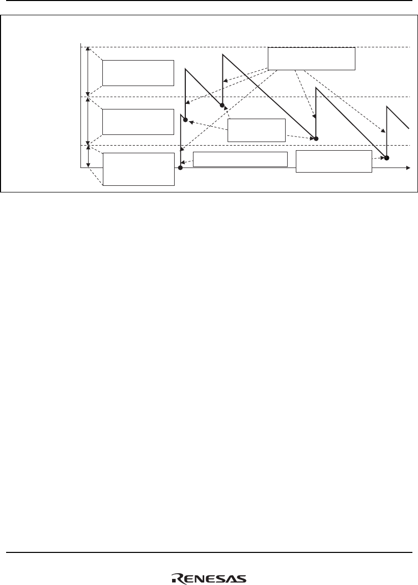
12. DDR2-SDRAM Interface (DBSC2)
Rev.1.00 Jan. 10, 2008 Page 521 of 1658
REJ09B0261-0100
LV1TH
LV0TH
0
Time
Refresh counter
value
Max. value
(Average refresh interval
+ LV1TH)
Level 1
(Refreshing during
request empty cycles)
Level 0
(Refreshing in vacant
periods between
SHwy commands)
Level 2
(Refreshing not done)
Refreshing is done immediately
after auto-refresh is enabled
Refreshing is done in
vacant periods between
SHwy commands
Refreshing is done
during request
empty cycles
The counter value increments
by the amount of
the average refresh interval
Figure 12.7 Relation between Auto-Refresh Operation and Threshold Values
12.5.6 Regarding Address Multiplexing
Memory of various sizes can be connected through the settings of the SDRAM configuration
register (DBCONF). The BWIDTH bits are used to set the external data bus width, and the SPLIT
bit is used to set the size of the memory connected. The BASFT bit setting is used to move the
position of the bank address toward the lower bits; depending on the application the possibility of
page hits may be increased.

12. DDR2-SDRAM Interface (DBSC2)
Rev.1.00 Jan. 10, 2008 Page 522 of 1658
REJ09B0261-0100
Table 12.12 Relation between SDRAM Address Pins and Logical Addresses when the
External Data Bus Width Is Set to 16 Bits (BASFT = 00)
(When Using a 16-Bit Product, One Is Connected; for 8-Bit Products, Two Are
Connected)
Memory
Type
MBA
2
MBA
1
MBA
0 MA14 MA13 MA12 MA11 MA10 MA9 MA8 MA7 MA6 MA5 MA4 MA3 MA2 MA1 MA0
ROW ⎯ A11 A10 ⎯ ⎯ A24 A23 A22 A21 A20 A19 A18 A17 A16 A15 A14 A13 A12 16M×
16b COL ⎯ A11 A10 ⎯ ⎯ ⎯ ⎯ ⎯ ⎯ A9 A8 A7 A6 A5 A4 A3 A2 A1
ROW ⎯ A12 A11 ⎯ ⎯ A25 A24 A23 A22 A21 A20 A19 A18 A17 A16 A15 A14 A13 32M×
8b COL ⎯ A12 A11 ⎯ ⎯ ⎯ ⎯ ⎯ A10 A9 A8 A7 A6 A5 A4 A3 A2 A1
ROW ⎯ A12 A11 ⎯ ⎯ A25 A24 A23 A22 A21 A20 A19 A18 A17 A16 A15 A14 A13 32M×
16b COL ⎯ A12 A11 ⎯ ⎯ ⎯ ⎯ ⎯ A10 A9 A8 A7 A6 A5 A4 A3 A2 A1
ROW ⎯ A12 A11 ⎯ A26 A25 A24 A23 A22 A21 A20 A19 A18 A17 A16 A15 A14 A13 64M×
8b COL ⎯ A12 A11 ⎯ ⎯ ⎯ ⎯ ⎯ A10 A9 A8 A7 A6 A5 A4 A3 A2 A1
ROW A11 A12 A13 ⎯ ⎯ A26 A25 A24 A23 A22 A21 A20 A19 A18 A17 A16 A15 A14 64M×
16b COL A11 A12 A13 ⎯ ⎯ ⎯ ⎯ ⎯ A10 A9 A8 A7 A6 A5 A4 A3 A2 A1
ROW A11 A12 A13 ⎯ A27 A26 A25 A24 A23 A22 A21 A20 A19 A18 A17 A16 A15 A14 128M
×8b COL A11 A12 A13 ⎯ ⎯ ⎯ ⎯ ⎯ A10 A9 A8 A7 A6 A5 A4 A3 A2 A1
ROW A11 A12 A13 ⎯ A27 A26 A25 A24 A23 A22 A21 A20 A19 A18 A17 A16 A15 A14 128M
×16b COL A11 A12 A13 ⎯ ⎯ ⎯ ⎯ ⎯ A10 A9 A8 A7 A6 A5 A4 A3 A2 A1
ROW A11 A12 A13 A28 A27 A26 A25 A24 A23 A22 A21 A20 A19 A18 A17 A16 A15 A14 256M
×8b COL A11 A12 A13 ⎯ ⎯ ⎯ ⎯ ⎯ A10 A9 A8 A7 A6 A5 A4 A3 A2 A1

12. DDR2-SDRAM Interface (DBSC2)
Rev.1.00 Jan. 10, 2008 Page 523 of 1658
REJ09B0261-0100
Table 12.13 Relation between SDRAM Address Pins and Logical Addresses when the
External Data Bus Width Is Set to 32 Bits (BASFT = 00)
(When Using 16-Bit Products, Two Are Connected; for 8-Bit Products, Four
Are Connected)
Memory
Type
MBA
2
MBA
1
MBA
0 MA14 MA13 MA12 MA11 MA10 MA9 MA8 MA7 MA6 MA5 MA4 MA3 MA2 MA1 MA0
ROW ⎯ A12 A11 ⎯ ⎯ A25 A24 A23 A22 A21 A20 A19 A18 A17 A16 A15 A14 A13 16M×
16b COL ⎯ A12 A11 ⎯ ⎯ ⎯ ⎯ ⎯ ⎯ A10 A9 A8 A7 A6 A5 A4 A3 A2
ROW ⎯ A12 A13 ⎯ A26 A25 A24 A23 A22 A21 A20 A19 A18 A17 A16 A15 A14 32M×
8b COL ⎯ A12 A13 ⎯ ⎯ ⎯ ⎯ ⎯ A11 A10 A9 A8 A7 A6 A5 A4 A3 A2
ROW ⎯ A12 A13 ⎯ ⎯ A26 A25 A24 A23 A22 A21 A20 A19 A18 A17 A16 A15 A14 32M×
16b COL ⎯ A12 A13 ⎯ ⎯ ⎯ ⎯ ⎯ A11 A10 A9 A8 A7 A6 A5 A4 A3 A2
ROW ⎯ A12 A13 ⎯ A27 A26 A25 A24 A23 A22 A21 A20 A19 A18 A17 A16 A15 A14 64M×
8b COL ⎯ A12 A13 ⎯ ⎯ ⎯ ⎯ ⎯ A11 A10 A9 A8 A7 A6 A5 A4 A3 A2
ROW A14 A12 A13 ⎯ ⎯ A27 A26 A25 A24 A23 A22 A21 A20 A19 A18 A17 A16 A15 64M×
16b COL A14 A12 A13 ⎯ ⎯ ⎯ ⎯ ⎯ A11 A10 A9 A8 A7 A6 A5 A4 A3 A2
ROW A14 A12 A13 ⎯ A28 A27 A26 A25 A24 A23 A22 A21 A20 A19 A18 A17 A16 A15 128M
×8b COL A14 A12 A13 ⎯ ⎯ ⎯ ⎯ ⎯ A11 A10 A9 A8 A7 A6 A5 A4 A3 A2
ROW A14 A12 A13 ⎯ A28 A27 A26 A25 A24 A23 A22 A21 A20 A19 A18 A17 A16 A15 128M
×16b COL A14 A12 A13 ⎯ ⎯ ⎯ ⎯ ⎯ A11 A10 A9 A8 A7 A6 A5 A4 A3 A2
ROW A14 A12 A13 A29 A28 A27 A26 A25 A24 A23 A22 A21 A20 A19 A18 A17 A16 A15 256M
×8b COL A14 A12 A13 ⎯ ⎯ ⎯ ⎯ ⎯ A11 A10 A9 A8 A7 A6 A5 A4 A3 A2

12. DDR2-SDRAM Interface (DBSC2)
Rev.1.00 Jan. 10, 2008 Page 524 of 1658
REJ09B0261-0100
Table 12.14 Relation between SDRAM Address Pins and Logical Addresses when the
External Data Bus Width Is Set to 16 Bits (BASFT = 01)
(When Using a 16-Bit Product, One Is Connected; for 8-Bit Products, Two Are
Connected)
Memory
Type
MBA
2
MBA
1
MBA
0 MA14 MA13 MA12 MA11 MA10 MA9 MA8 MA7 MA6 MA5 MA4 MA3 MA2 MA1 MA0
ROW ⎯ A10 A9 ⎯ ⎯ A24 A23 A22 A21 A20 A19 A18 A17 A16 A15 A14 A13 A12 16M×
16b COL ⎯ A10 A9 ⎯ ⎯ ⎯ ⎯ ⎯ ⎯ A11 A8 A7 A6 A5 A4 A3 A2 A1
ROW ⎯ A11 A10 ⎯ ⎯ A25 A24 A23 A22 A21 A20 A19 A18 A17 A16 A15 A14 A13 32M×
8b COL ⎯ A11 A10 ⎯ ⎯ ⎯ ⎯ ⎯ A12 A9 A8 A7 A6 A5 A4 A3 A2 A1
ROW ⎯ A11 A10 ⎯ ⎯ A25 A24 A23 A22 A21 A20 A19 A18 A17 A16 A15 A14 A13 32M×
16b COL ⎯ A11 A10 ⎯ ⎯ ⎯ ⎯ ⎯ A12 A9 A8 A7 A6 A5 A4 A3 A2 A1
ROW ⎯ A11 A10 ⎯ A26 A25 A24 A23 A22 A21 A20 A19 A18 A17 A16 A15 A14 A13 64M×
8b COL ⎯ A11 A10 ⎯ ⎯ ⎯ ⎯ ⎯ A12 A9 A8 A7 A6 A5 A4 A3 A2 A1
ROW A10 A11 A12 ⎯ ⎯ A26 A25 A24 A23 A22 A21 A20 A19 A18 A17 A16 A15 A14 64M×
16b COL A10 A11 A12 ⎯ ⎯ ⎯ ⎯ ⎯ A13 A9 A8 A7 A6 A5 A4 A3 A2 A1
ROW A10 A11 A12 ⎯ A27 A26 A25 A24 A23 A22 A21 A20 A19 A18 A17 A16 A15 A14 128M
×8b COL A10 A11 A12 ⎯ ⎯ ⎯ ⎯ ⎯ A13 A9 A8 A7 A6 A5 A4 A3 A2 A1
ROW A10 A11 A12 ⎯ A27 A26 A25 A24 A23 A22 A21 A20 A19 A18 A17 A16 A15 A14 128M
×16b COL A10 A11 A12 ⎯ ⎯ ⎯ ⎯ ⎯ A13 A9 A8 A7 A6 A5 A4 A3 A2 A1
ROW A10 A11 A12 A28 A27 A26 A25 A24 A23 A22 A21 A20 A19 A18 A17 A16 A15 A14 256M
×8b COL A10 A11 A12 ⎯ ⎯ ⎯ ⎯ ⎯ A13 A9 A8 A7 A6 A5 A4 A3 A2 A1

12. DDR2-SDRAM Interface (DBSC2)
Rev.1.00 Jan. 10, 2008 Page 525 of 1658
REJ09B0261-0100
Table 12.15 Relation between SDRAM Address Pins and Logical Addresses when the
External Data Bus Width Is Set to 32 Bits (BASFT = 01)
(When Using 16-Bit Products, Two Are Connected; for 8-Bit Products, Four
Are Connected)
Memory
Type
MBA
2
MBA
1
MBA
0 MA14 MA13 MA12 MA11 MA10 MA9 MA8 MA7 MA6 MA5 MA4 MA3 MA2 MA1 MA0
ROW ⎯ A11 A10 ⎯ ⎯ A25 A24 A23 A22 A21 A20 A19 A18 A17 A16 A15 A14 A13 16M×
16b COL ⎯ A11 A10 ⎯ ⎯ ⎯ ⎯ ⎯ ⎯ A12 A9 A8 A7 A6 A5 A4 A3 A2
ROW ⎯ A11 A12 ⎯ A26 A25 A24 A23 A22 A21 A20 A19 A18 A17 A16 A15 A14 32M×
8b COL ⎯ A11 A12 ⎯ ⎯ ⎯ ⎯ ⎯ A13 A10 A9 A8 A7 A6 A5 A4 A3 A2
ROW ⎯ A11 A12 ⎯ ⎯ A26 A25 A24 A23 A22 A21 A20 A19 A18 A17 A16 A15 A14 32M×
16b COL ⎯ A11 A12 ⎯ ⎯ ⎯ ⎯ ⎯ A13 A10 A9 A8 A7 A6 A5 A4 A3 A2
ROW ⎯ A11 A12 ⎯ A27 A26 A25 A24 A23 A22 A21 A20 A19 A18 A17 A16 A15 A14 64M×
8b COL ⎯ A11 A12 ⎯ ⎯ ⎯ ⎯ ⎯ A13 A10 A9 A8 A7 A6 A5 A4 A3 A2
ROW A13 A11 A12 ⎯ ⎯ A27 A26 A25 A24 A23 A22 A21 A20 A19 A18 A17 A16 A15 64M×
16b COL A13 A11 A12 ⎯ ⎯ ⎯ ⎯ ⎯ A14 A10 A9 A8 A7 A6 A5 A4 A3 A2
ROW A13 A11 A12 ⎯ A28 A27 A26 A25 A24 A23 A22 A21 A20 A19 A18 A17 A16 A15 128M
×8b COL A13 A11 A12 ⎯ ⎯ ⎯ ⎯ ⎯ A14 A10 A9 A8 A7 A6 A5 A4 A3 A2
ROW A13 A11 A12 ⎯ A28 A27 A26 A25 A24 A23 A22 A21 A20 A19 A18 A17 A16 A15 128M
×16b COL A13 A11 A12 ⎯ ⎯ ⎯ ⎯ ⎯ A14 A10 A9 A8 A7 A6 A5 A4 A3 A2
ROW A13 A11 A12 A29 A28 A27 A26 A25 A24 A23 A22 A21 A20 A19 A18 A17 A16 A15 256M
×8b COL A13 A11 A12 ⎯ ⎯ ⎯ ⎯ ⎯ A14 A10 A9 A8 A7 A6 A5 A4 A3 A2

12. DDR2-SDRAM Interface (DBSC2)
Rev.1.00 Jan. 10, 2008 Page 526 of 1658
REJ09B0261-0100
Table 12.16 Relation between SDRAM Address Pins and Logical Addresses when the
External Data Bus Width Is Set to 16 Bits (BASFT = 10)
(When Using a 16-Bit Product, One Is Connected; for 8-Bit Products, Two Are
Connected)
Memory
Type
MBA
2
MBA
1
MBA
0 MA14 MA13 MA12 MA11 MA10 MA9 MA8 MA7 MA6 MA5 MA4 MA3 MA2 MA1 MA0
ROW ⎯ A9 A8 ⎯ ⎯ A24 A23 A22 A21 A20 A19 A18 A17 A16 A15 A14 A13 A12 16M×
16b COL ⎯ A9 A8 ⎯ ⎯ ⎯ ⎯ ⎯ ⎯ A11 A10 A7 A6 A5 A4 A3 A2 A1
ROW ⎯ A10 A9 ⎯ ⎯ A25 A24 A23 A22 A21 A20 A19 A18 A17 A16 A15 A14 A13 32M×
8b COL ⎯ A10 A9 ⎯ ⎯ ⎯ ⎯ ⎯ A12 A11 A8 A7 A6 A5 A4 A3 A2 A1
ROW ⎯ A10 A9 ⎯ ⎯ A25 A24 A23 A22 A21 A20 A19 A18 A17 A16 A15 A14 A13 32M×
16b COL ⎯ A10 A9 ⎯ ⎯ ⎯ ⎯ ⎯ A12 A11 A8 A7 A6 A5 A4 A3 A2 A1
ROW ⎯ A10 A9 ⎯ A26 A25 A24 A23 A22 A21 A20 A19 A18 A17 A16 A15 A14 A13 64M×
8b COL ⎯ A10 A9 ⎯ ⎯ ⎯ ⎯ ⎯ A12 A11 A8 A7 A6 A5 A4 A3 A2 A1
ROW A9 A10 A11 ⎯ ⎯ A26 A25 A24 A23 A22 A21 A20 A19 A18 A17 A16 A15 A14 64M×
16b COL A9 A10 A11 ⎯ ⎯ ⎯ ⎯ ⎯ A13 A12 A8 A7 A6 A5 A4 A3 A2 A1
ROW A9 A10 A11 ⎯ A27 A26 A25 A24 A23 A22 A21 A20 A19 A18 A17 A16 A15 A14 128M
×8b COL A9 A10 A11 ⎯ ⎯ ⎯ ⎯ ⎯ A13 A12 A8 A7 A6 A5 A4 A3 A2 A1
ROW A9 A10 A11 ⎯ A27 A26 A25 A24 A23 A22 A21 A20 A19 A18 A17 A16 A15 A14 128M
×16b COL A9 A10 A11 ⎯ ⎯ ⎯ ⎯ ⎯ A13 A12 A8 A7 A6 A5 A4 A3 A2 A1
ROW A9 A10 A11 A28 A27 A26 A25 A24 A23 A22 A21 A20 A19 A18 A17 A16 A15 A14 256M
×8b COL A9 A10 A11 ⎯ ⎯ ⎯ ⎯ ⎯ A13 A12 A8 A7 A6 A5 A4 A3 A2 A1

12. DDR2-SDRAM Interface (DBSC2)
Rev.1.00 Jan. 10, 2008 Page 527 of 1658
REJ09B0261-0100
Table 12.17 Relation between SDRAM Address Pins and Logical Addresses when the
External Data Bus Width Is Set to 32 Bits (BASFT = 10)
(When Using 16-Bit Products, Two Are Connected; for 8-Bit Products, Four
Are Connected)
Memory
Type
MBA
2
MBA
1
MBA
0 MA14 MA13 MA12 MA11 MA10 MA9 MA8 MA7 MA6 MA5 MA4 MA3 MA2 MA1 MA0
ROW ⎯ A10 A9 ⎯ ⎯ A25 A24 A23 A22 A21 A20 A19 A18 A17 A16 A15 A14 A13 16M×
16b COL ⎯ A10 A9 ⎯ ⎯ ⎯ ⎯ ⎯ ⎯ A12 A11 A8 A7 A6 A5 A4 A3 A2
ROW ⎯ A10 A11 ⎯ A26 A25 A24 A23 A22 A21 A20 A19 A18 A17 A16 A15 A14 32M×
8b COL ⎯ A10 A11 ⎯ ⎯ ⎯ ⎯ ⎯ A13 A12 A9 A8 A7 A6 A5 A4 A3 A2
ROW ⎯ A10 A11 ⎯ ⎯ A26 A25 A24 A23 A22 A21 A20 A19 A18 A17 A16 A15 A14 32M×
16b COL ⎯ A10 A11 ⎯ ⎯ ⎯ ⎯ ⎯ A13 A12 A9 A8 A7 A6 A5 A4 A3 A2
ROW ⎯ A10 A11 ⎯ A27 A26 A25 A24 A23 A22 A21 A20 A19 A18 A17 A16 A15 A14 64M×
8b COL ⎯ A10 A11 ⎯ ⎯ ⎯ ⎯ ⎯ A13 A12 A9 A8 A7 A6 A5 A4 A3 A2
ROW A12 A10 A11 ⎯ ⎯ A27 A26 A25 A24 A23 A22 A21 A20 A19 A18 A17 A16 A15 64M×
16b COL A12 A10 A11 ⎯ ⎯ ⎯ ⎯ ⎯ A14 A13 A9 A8 A7 A6 A5 A4 A3 A2
ROW A12 A10 A11 ⎯ A28 A27 A26 A25 A24 A23 A22 A21 A20 A19 A18 A17 A16 A15 128M
×8b COL A12 A10 A11 ⎯ ⎯ ⎯ ⎯ ⎯ A14 A13 A9 A8 A7 A6 A5 A4 A3 A2
ROW A12 A10 A11 ⎯ A28 A27 A26 A25 A24 A23 A22 A21 A20 A19 A18 A17 A16 A15 128M
×16b COL A12 A10 A11 ⎯ ⎯ ⎯ ⎯ ⎯ A14 A13 A9 A8 A7 A6 A5 A4 A3 A2
ROW A12 A10 A11 A29 A28 A27 A26 A25 A24 A23 A22 A21 A20 A19 A18 A17 A16 A15 256M
×8b COL A12 A10 A11 ⎯ ⎯ ⎯ ⎯ ⎯ A14 A13 A9 A8 A7 A6 A5 A4 A3 A2

12. DDR2-SDRAM Interface (DBSC2)
Rev.1.00 Jan. 10, 2008 Page 528 of 1658
REJ09B0261-0100
Table 12.18 Relation between SDRAM Address Pins and Logical Addresses when the
External Data Bus Width Is Set to 16 Bits (BASFT = 11)
(When Using a 16-Bit Product, One Is Connected; for 8-Bit Products, Two Are
Connected)
Memory
Type
MBA
2
MBA
1
MBA
0 MA14 MA13 MA12 MA11 MA10 MA9 MA8 MA7 MA6 MA5 MA4 MA3 MA2 MA1 MA0
ROW ⎯ A8 A7 ⎯ ⎯ A24 A23 A22 A21 A20 A19 A18 A17 A16 A15 A14 A13 A12 16M×
16b COL ⎯ A8 A7 ⎯ ⎯ ⎯ ⎯ ⎯ ⎯ A11 A10 A9 A6 A5 A4 A3 A2 A1
ROW ⎯ A9 A8 ⎯ ⎯ A25 A24 A23 A22 A21 A20 A19 A18 A17 A16 A15 A14 A13 32M×
8b COL ⎯ A9 A8 ⎯ ⎯ ⎯ ⎯ ⎯ A12 A11 A10 A7 A6 A5 A4 A3 A2 A1
ROW ⎯ A9 A8 ⎯ ⎯ A25 A24 A23 A22 A21 A20 A19 A18 A17 A16 A15 A14 A13 32M×
16b COL ⎯ A9 A8 ⎯ ⎯ ⎯ ⎯ ⎯ A12 A11 A10 A7 A6 A5 A4 A3 A2 A1
ROW ⎯ A9 A8 ⎯ A26 A25 A24 A23 A22 A21 A20 A19 A18 A17 A16 A15 A14 A13 64M×
8b COL ⎯ A9 A8 ⎯ ⎯ ⎯ ⎯ ⎯ A12 A11 A10 A7 A6 A5 A4 A3 A2 A1
ROW A8 A9 A10 ⎯ ⎯ A26 A25 A24 A23 A22 A21 A20 A19 A18 A17 A16 A15 A14 64M×
16b COL A8 A9 A10 ⎯ ⎯ ⎯ ⎯ ⎯ A13 A12 A11 A7 A6 A5 A4 A3 A2 A1
ROW A8 A9 A10 ⎯ A27 A26 A25 A24 A23 A22 A21 A20 A19 A18 A17 A16 A15 A14 128M
×8b COL A8 A9 A10 ⎯ ⎯ ⎯ ⎯ ⎯ A13 A12 A11 A7 A6 A5 A4 A3 A2 A1
ROW A8 A9 A10 ⎯ A27 A26 A25 A24 A23 A22 A21 A20 A19 A18 A17 A16 A15 A14 128M
×16b COL A8 A9 A10 ⎯ ⎯ ⎯ ⎯ ⎯ A13 A12 A11 A7 A6 A5 A4 A3 A2 A1
ROW A8 A9 A10 A28 A27 A26 A25 A24 A23 A22 A21 A20 A19 A18 A17 A16 A15 A14 256M
×8b COL A8 A9 A10 ⎯ ⎯ ⎯ ⎯ ⎯ A13 A12 A11 A7 A6 A5 A4 A3 A2 A1

12. DDR2-SDRAM Interface (DBSC2)
Rev.1.00 Jan. 10, 2008 Page 529 of 1658
REJ09B0261-0100
Table 12.19 Relation between SDRAM Address Pins and Logical Addresses when the
External Data Bus Width Is Set to 32 Bits (BASFT = 11)
(When Using 16-bit Products, Two Are Connected; for 8-Bit Products, Four
Are Connected)
Memory
Type
MBA
2
MBA
1
MBA
0 MA14 MA13 MA12 MA11 MA10 MA9 MA8 MA7 MA6 MA5 MA4 MA3 MA2 MA1 MA0
ROW ⎯ A9 A8 ⎯ ⎯ A25 A24 A23 A22 A21 A20 A19 A18 A17 A16 A15 A14 A13 16M×
16b COL ⎯ A9 A8 ⎯ ⎯ ⎯ ⎯ ⎯ ⎯ A12 A11 A10 A7 A6 A5 A4 A3 A2
ROW ⎯ A9 A10 ⎯ A26 A25 A24 A23 A22 A21 A20 A19 A18 A17 A16 A15 A14 32M×
8b COL ⎯ A9 A10 ⎯ ⎯ ⎯ ⎯ ⎯ A13 A12 A11 A8 A7 A6 A5 A4 A3 A2
ROW ⎯ A9 A10 ⎯ ⎯ A26 A25 A24 A23 A22 A21 A20 A19 A18 A17 A16 A15 A14 32M×
16b COL ⎯ A9 A10 ⎯ ⎯ ⎯ ⎯ ⎯ A13 A12 A11 A8 A7 A6 A5 A4 A3 A2
ROW ⎯ A9 A10 ⎯ A27 A26 A25 A24 A23 A22 A21 A20 A19 A18 A17 A16 A15 A14 64M×
8b COL ⎯ A9 A10 ⎯ ⎯ ⎯ ⎯ ⎯ A13 A12 A11 A8 A7 A6 A5 A4 A3 A2
ROW A11 A9 A10 ⎯ ⎯ A27 A26 A25 A24 A23 A22 A21 A20 A19 A18 A17 A16 A15 64M×
16b COL A11 A9 A10 ⎯ ⎯ ⎯ ⎯ ⎯ A14 A13 A12 A8 A7 A6 A5 A4 A3 A2
ROW A11 A9 A10 ⎯ A28 A27 A26 A25 A24 A23 A22 A21 A20 A19 A18 A17 A16 A15 128M
×8b COL A11 A9 A10 ⎯ ⎯ ⎯ ⎯ ⎯ A14 A13 A12 A8 A7 A6 A5 A4 A3 A2
ROW A11 A9 A10 ⎯ A28 A27 A26 A25 A24 A23 A22 A21 A20 A19 A18 A17 A16 A15 128M
×16b COL A11 A9 A10 ⎯ ⎯ ⎯ ⎯ ⎯ A14 A13 A12 A8 A7 A6 A5 A4 A3 A2
ROW A11 A9 A10 A29 A28 A27 A26 A25 A24 A23 A22 A21 A20 A19 A18 A17 A16 A15 256M
×8b COL A11 A9 A10 ⎯ ⎯ ⎯ ⎯ ⎯ A14 A13 A12 A8 A7 A6 A5 A4 A3 A2

12. DDR2-SDRAM Interface (DBSC2)
Rev.1.00 Jan. 10, 2008 Page 530 of 1658
REJ09B0261-0100
12.5.7 Regarding SDRAM Access and Timing Constraints
In this section, waveforms at the various pins during basic DDR2-SDRAM access are explained
first and then the relation between DDR2-SDRAM access and the CAS latency (CL), tRAS, tRFC,
tRCD, tRP, tRRD, tWR, tRTP, tRC, READ-WRITE minimum interval, WRITE-READ minimum
interval set using the SDRAM timing registers 0 to 2 (DBTR0 to DBTR2) is explained.
(1) Basic SDRAM Access
In this section, waveforms at the various pins during basic SDRAM access, including reading,
writing, auto-refresh, and self-refresh operations, are explained.
For the relation between writing and the ODT control signal output, refer to section 12.5.9,
Important Information Regarding ODT Control Signal Output to SDRAM.
Figure 12.8 shows waveforms for 1/2/4/8/16-byte reading when the bus width is set to 32 bits. In
this case, single-reading is performed in which the READ command is issued once. In this
example, read access processing is executed for bank A after the ACT command is issued, but
when there is a page hit, access begins with the issue of the READ command.
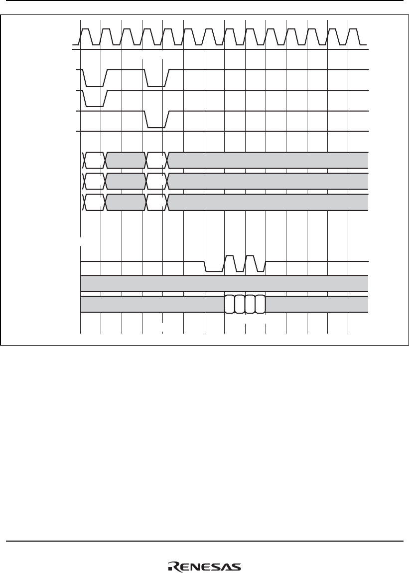
12. DDR2-SDRAM Interface (DBSC2)
Rev.1.00 Jan. 10, 2008 Page 531 of 1658
REJ09B0261-0100
MCK0,
MCK1
MA[14:11]
MA[9:0]
MBA[2:0]
MCKE
MCS
MRAS
MCAS
MWE
MA[10]
ACT
bank A bank A
Invalid
Invalid
Invalid
Invalid
MDQS[3:0]
MDQ[31:0]
MDM[3:0] Invalid
Invalid Invalid
SDRAM
command
Invalid
Invalid
Example of CL = 3
Valid
Valid
Valid
Valid
Valid
Valid
High level
READ
Read data
Figure 12.8 Waveforms for 1/2/4/8/16-Byte Reading
(When the Bus Width Is Set to 32 Bits)
Figure 12.9 shows waveforms for 32-byte reading when the bus width is set to 32 bits. In this case,
the READ command is issued twice. In this example, read access processing is executed for bank
A after the ACT command is issued, but when there is a page hit, access begins with the issue of
the READ command.
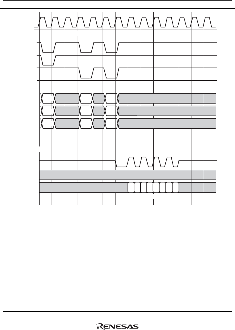
12. DDR2-SDRAM Interface (DBSC2)
Rev.1.00 Jan. 10, 2008 Page 532 of 1658
REJ09B0261-0100
MCK0,
MCK1
MA[14:11 ]
MA[9:0]
MBA[2:0]
MCKE
MCS
MRAS
MCAS
MWE
MA[10]
ACT
bank A
READ
bank A
Invalid Invalid
MDQS[3:0]
MDQ[31:0]
MDM[3:0] Invalid
Invalid Invalid
SDRAM
command
ValidInvalid
READ
bank A
Invalid InvalidValidInvalid
Invalid InvalidValid
Invalid
Valid Valid
Valid Valid
Valid Valid
High level
Example of CL = 3
Read data
Figure 12.9 Waveforms for 32-Byte Reading
(When the Bus Width Is Set to 32 Bits)
Figure 12.10 shows waveforms for 1/2/4/8/16-byte writing when the bus width is set to 32 bits. In
this case, single-writing is performed in which the WRITE command is issued once. In this
example, write access processing is executed for bank A after the ACT command is issued, but
when there is a page hit, access begins with the issue of the WRITE command.
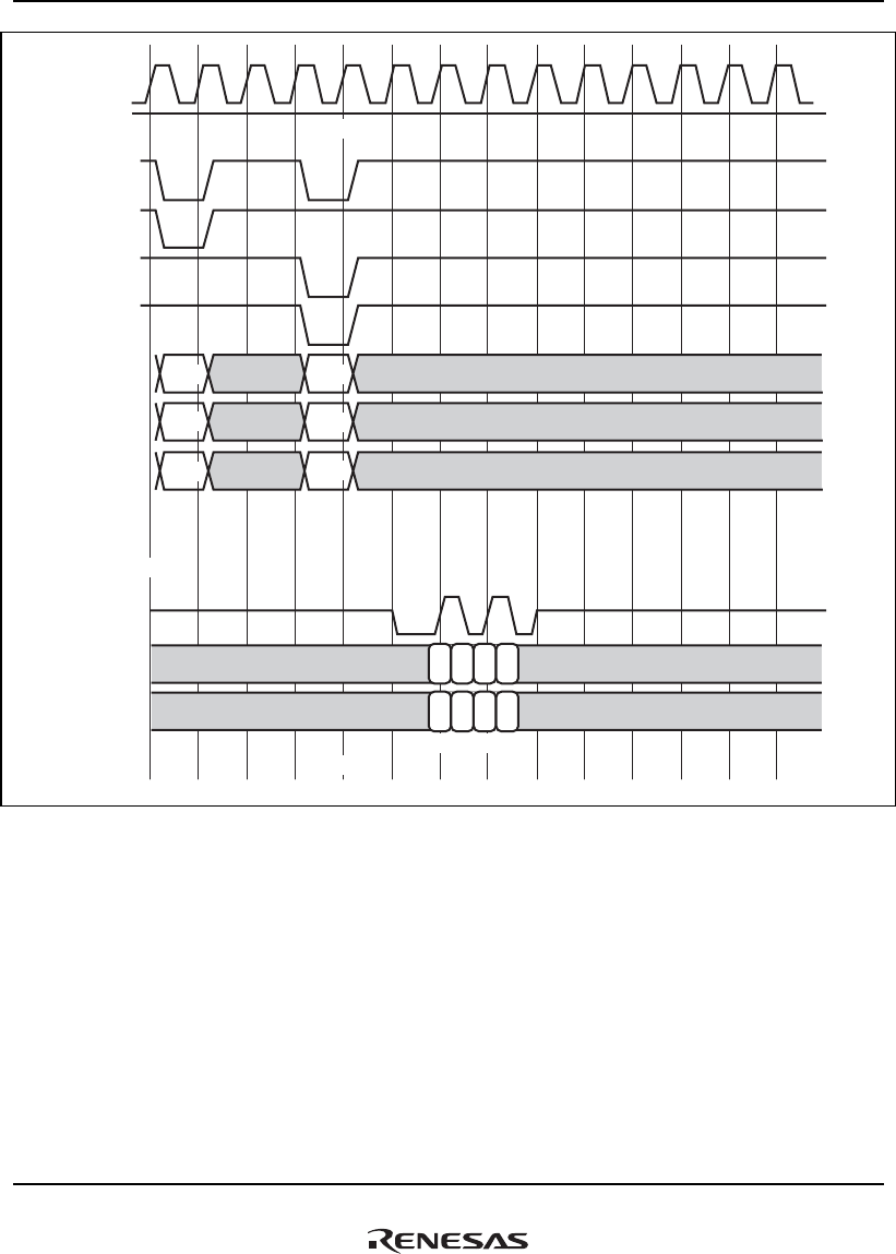
12. DDR2-SDRAM Interface (DBSC2)
Rev.1.00 Jan. 10, 2008 Page 533 of 1658
REJ09B0261-0100
MCK0,
MCK1
MA[14:11]
MA[9:0]
MBA[2:0]
MCKE
MCS
MRAS
MCAS
MWE
MA[10]
ACT
bank A bank A
Invalid
Invalid
Invalid
Invalid
MDQS[3:0]
MDQ[31:0]
MDM[3:0]
Invalid Invalid
SDRAM
command
Invalid
Invalid
Invalid Invalid
Valid
Valid
Valid
Valid
Valid
Valid
High level
Example of CL = 3
Write data
WRITE
Figure 12.10 Waveforms for 1/2/4/8/16-Byte Writing
(When the Bus Width Is Set to 32 Bits)
Figure 12.11 shows waveforms for 32-byte writing when the bus width is set to 32 bits. In this
case, the WRITE command is issued twice. In this example, write access processing is executed
for bank A after the ACT command is issued, but when there is a page hit, access begins with the
issue of the WRITE command.
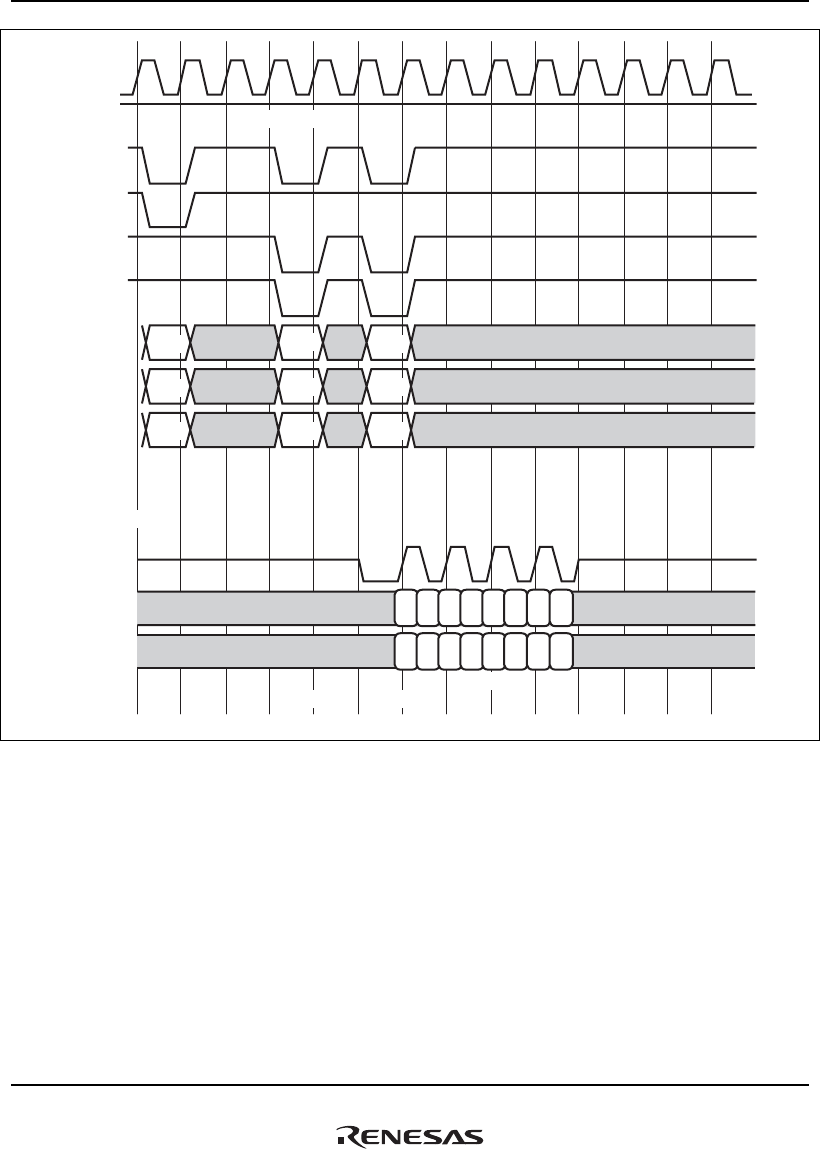
12. DDR2-SDRAM Interface (DBSC2)
Rev.1.00 Jan. 10, 2008 Page 534 of 1658
REJ09B0261-0100
MCK0,
MCK1
MA[14:11]
MA[9:0]
MBA[2:0]
MCKE
MCS
MRAS
MCAS
MWE
MA[10]
ACT
bank A bank A
Invalid Invalid
MDQS[3:0]
MDQ[31:0]
MDM[3:0]
Invalid Invalid
SDRAM
command
Invalid
Invalid Invalid
Invalid InvalidInvalid
Invalid InvalidInvalid
Example of CL = 3
Valid Valid
Valid Valid
Valid Valid
Write data
bank A
WRITEWRITE
Valid
Valid
Valid
High level
Figure 12.11 Waveforms for 32-Byte Writing (When the Bus Width Is Set to 32 Bits)
Figure 12.12 shows waveforms during auto-refresh operation resulting from settings of the
SDRAM refresh control registers 0, 1, and 2. The DBSC2 issues a REF command automatically
after the PALL command is issued when at least one DDR2-SDRAM bank is activated before the
REF command. Consequently, there is no need to use software to manage precharging of all the
banks for the auto-refresh operation.
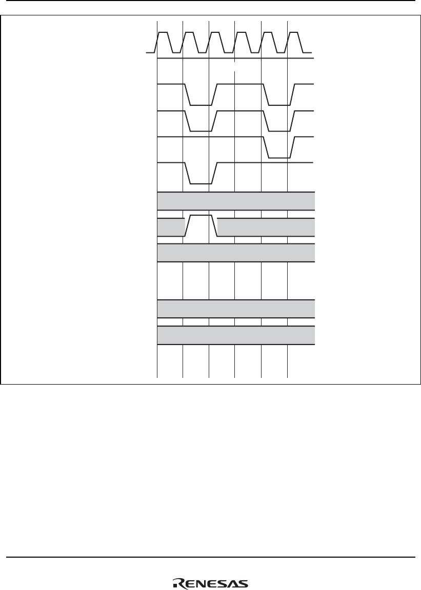
12. DDR2-SDRAM Interface (DBSC2)
Rev.1.00 Jan. 10, 2008 Page 535 of 1658
REJ09B0261-0100
MCK0,
MCK1
MA[14:11]
MA[9:0]
MBA[2:0]
MCKE
MCS
MRAS
MCAS
MWE
MA[10]
Invalid
MDQS[3:0]
MDQ[31:0]
MDM[3:0] Invalid
Invalid
Invalid
Invalid
PALL
Invalid
REF
SDRAM
command
High level
Figure 12.12 Auto-Refresh Operation
Figure 12.13 shows the self-refresh operation. In order to perform self-refresh operation, the
sequence must be observed. For details, refer to section 12.5.4, Self-Refresh Operation.
When performing processing according to the sequence in section 12.5.4, Self-Refresh Operation,
commands to be issued to the SDRAM are those shown in figure 12.13. Before the transition to
self-refresh, the PALL command is issued in software. Then, software is used to issue the REF
command, and the SLFRSH (self-refresh entry from IDLE) command is issued. The SDRAM
continues in self-refresh mode until self-refresh is cancelled in software. After issuing the
SLFRSHX (self-refresh exit) command in software, it is necessary to wait for the time (tXSNR)
specified in the datasheet for the SDRAM being used until issuing a REF command. A wait
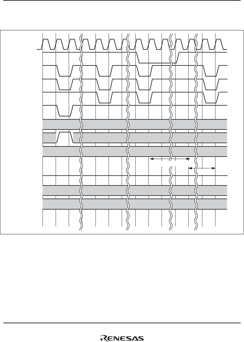
12. DDR2-SDRAM Interface (DBSC2)
Rev.1.00 Jan. 10, 2008 Page 536 of 1658
REJ09B0261-0100
example is shown in section 12.5.11, Method for Securing Time Required for Initialization, Self-
Refresh Cancellation, etc.
RSHX
MCK0,
MCK1
MA[14:11]
MA[9:0]
MBA[2:0]
MCKE
MCS
MRAS
MCAS
MWE
MA[10]
Invalid
MDQS[3:0]
MDQ[31:0]
MDM[3:0] Invalid
Invalid
Invalid
Invalid
PALL
Invalid
SLFRSH
SDRAM
command
SLF REFREF
tXSNR
Self-refresh in progress
Figure 12.13 Self-Refresh Operation
(2) Regarding Timing Constraints
Figure 12.14 shows the relation between the settings of CL, tRAS, tRCD, and tRP, and the issuing
of commands. Figure 12.15 shows the relation to tRRD and tRTP, figure 12.16 shows the relation
to tWR, figure 12.17 shows the relation to tRC, figure 12.18 shows the relation to READ-WRITE,
figure 12.19 shows the relation to WRITE-READ, and figure 12.20 shows the relation to tRFC.
Figure 12.14 corresponds to operation in a case in which, with bank A open, there is read access of
bank A and a page miss occurs. The constraint tRP between the PRE command and ACT
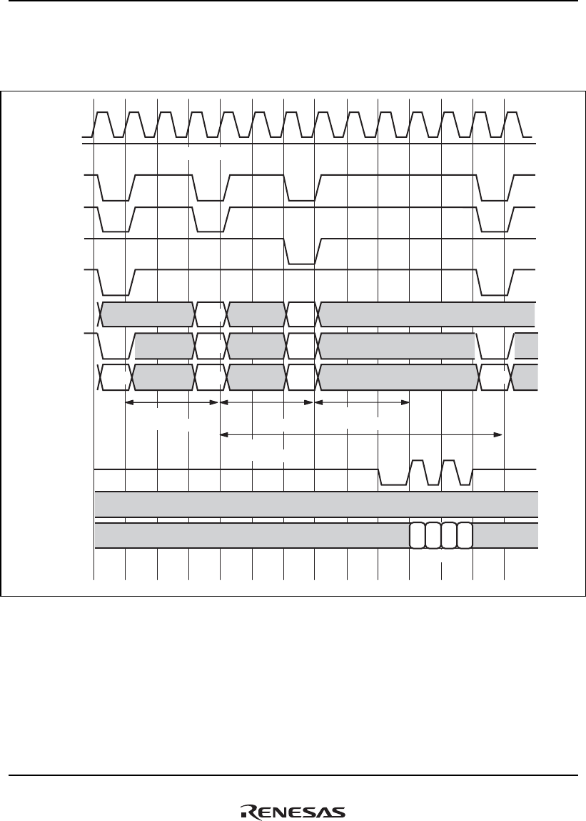
12. DDR2-SDRAM Interface (DBSC2)
Rev.1.00 Jan. 10, 2008 Page 537 of 1658
REJ09B0261-0100
command, the constraint tRCD between the ACT command and READ command, and the
constraint tRAS between the ACT command and the PRE command are involved. The DBSC2
waits to issue commands until each of the constraints is satisfied.
MCK0,
MCK1
MA[14:11]
MA[9:0]
MBA[2:0]
MCKE
MCS
MRAS
MCAS
MWE
MA[10]
PRE
bank A
ACT
bank A
Valid
Valid
Valid
Invalid
READ
bank A
tRCD
Invalid
Invalid
Invalid
Invalid
Invalid
Invalid
Invalid
Invalid
MDQS[3:0]
MDQ[31:0]
MDM[3:0] Invalid
Invalid Invalid
Invalid
Invalid
PRE
bank A
SDRAM
command
Valid
ValidValid
Valid
Valid
High level
CL
= 3 cycles= 3 cycles
tRAS
= 9 cycles
tRP
= 3 cycles
Read data
Figure 12.14 tRP, tRCD, CL, and tRAS

12. DDR2-SDRAM Interface (DBSC2)
Rev.1.00 Jan. 10, 2008 Page 538 of 1658
REJ09B0261-0100
MCK0,
MCK1
MA[14:11]
MA[9:0]
MBA[2:0]
MCKE
MCS
MRAS
MCAS
MWE
MA[10]
ACT
bank A
READ
bank A
Invalid
Invalid
Invalid
Invalid
Invalid
Invalid
MDQS[3:0]
MDQ[31:0]
MDM[3:0] Invalid
Invalid Invalid
Valid
PRE
bank C
Valid
Valid
Valid
ACT
bank B
READ
bank B
READ
bank C
Invalid
Invalid
Invalid
Invalid
Invalid
Invalid
Valid
Valid
Valid
SDRAM
command
Valid
Valid
Valid
ACT
bank C
Invalid
Invalid
Invalid
Invalid
Invalid
tRTP
= 2 cycles
Read data
tRRD
= 2 cycles
Example of CL = 3
Valid
Valid
Valid
Valid
Valid
Valid
Valid
Valid
Valid
High level
Figure 12.15 tRRD and tRTP
Figure 12.15 shows a case in which the pages for both of banks A and B are closed, the page for
bank C is open, and a page hit has occurred. When the tRRD time constraint has been satisfied
starting from issue of the ACT command for bank A, the ACT command for bank B is issued.
Because time tRCD has elapsed from the issue of the ACT command for bank A, a READ
command can be used. The READ command has a burst length of 4, so after two cycles a READ
command for bank B can be issued. A further two cycles later, a READ command for bank C can
be issued. However, the next request is access for which bank C must be closed, and so after the
elapse of time tRTP a PRE command is issued.
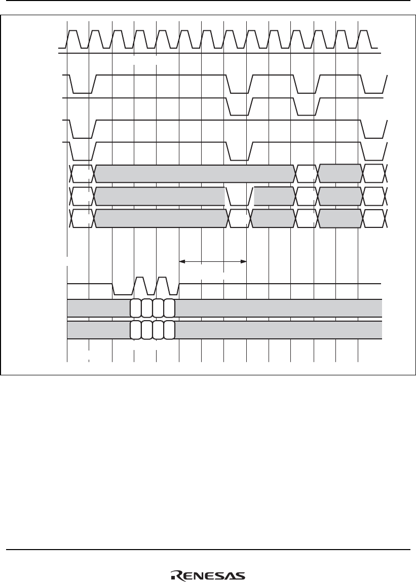
12. DDR2-SDRAM Interface (DBSC2)
Rev.1.00 Jan. 10, 2008 Page 539 of 1658
REJ09B0261-0100
MCK0,
MCK1
MA[14:11]
MA[9:0]
MBA[2:0]
MCKE
MCS
MRAS
MCAS
MWE
MA[10]
bank A
Invalid
MDQS[3:0]
MDQ[31:0]
MDM[3:0] Invalid
Invalid
Invalid
Invalid
PRE
bank A
Invalid
Invalid
Invalid
Invalid
SDRAM
command
ACT
bank A
Valid
Valid
Valid
Invalid
Invalid
Invalid
WRITE
bank A
Example of CL = 3
WRITE
Write data
tWR
= 3 cycles
Valid
Valid
Valid
Valid
Valid
Valid
Valid
High level
Figure 12.16 tWR
Figure 12.16 shows a case in which, after a write request, access occurs requiring that bank B be
closed. After the issue of a WRITE command, it is necessary to wait for time tWR or longer after
output of the write data before issuing a PRE command.
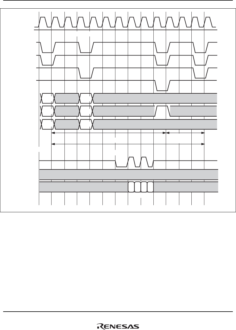
12. DDR2-SDRAM Interface (DBSC2)
Rev.1.00 Jan. 10, 2008 Page 540 of 1658
REJ09B0261-0100
MCK0,
MCK1
MA[14:11]
MA[9:0]
MBA[2:0]
MCKE
MCS
MRAS
MCAS
MWE
MA[10]
ACT
bank A
READ
bank A
Invalid
Invalid
Invalid
Invalid
MDQS[3:0]
MDQ[31:0]
MDM[3:0] Invalid
Invalid Invalid
Invalid
PALL
Invalid
Invalid
REF
SDRAM
command
tRAS
= 9 cycles
Read data
tRC
= 12 cycles
tRP
= 3 cycles
Example of CL = 3
Valid
Valid
Valid
Valid
Valid
Valid
High level
Figure 12.17 tRC
Figure 12.17 shows an example of performing auto-refresh after read access of bank A, the page
for which had been closed. After issuing an ACT command and READ command for bank A and
performing data reading, a PALL command must be used to close all banks in order to perform
auto-refresh. In order to issue the PALL command, the tRAS time constraint must be satisfied, and
issuing of the PALL command is delayed until this time. Then, when issuing the REF command,
both of time constraints tRP and tRC must be satisfied simultaneously. When these constraints are
both satisfied, the REF command is issued and auto-refresh is performed.
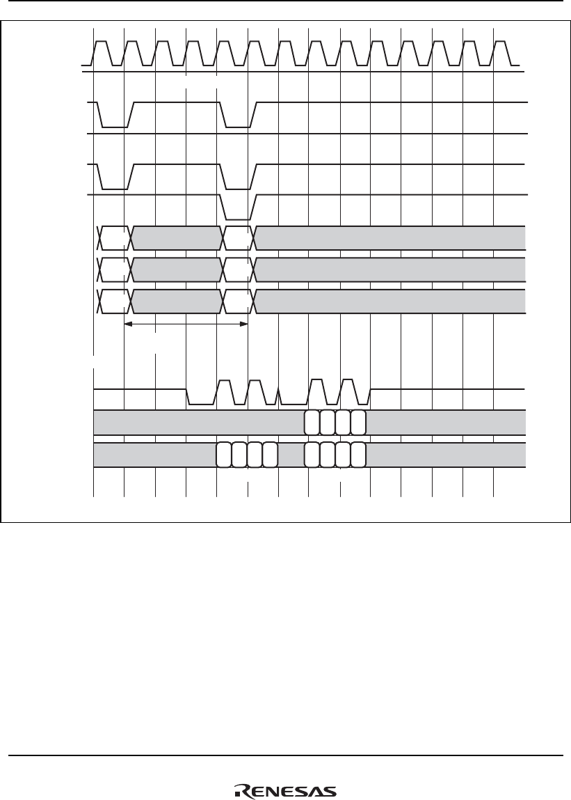
12. DDR2-SDRAM Interface (DBSC2)
Rev.1.00 Jan. 10, 2008 Page 541 of 1658
REJ09B0261-0100
MCK0,
MCK1
MA[14:11]
MA[9:0]
MBA[2:0]
MCKE
MCS
MRAS
MCAS
MWE
MA[10]
WRITE
any
bank
Invalid
MDQS[3:0]
MDQ[31:0]
MDM[3:0] Invalid
Invalid Invalid
Invalid
Invalid
READ
any
bank
Invalid
Invalid
Invalid
SDRAM
command
Invalid
Invalid
Write dataRead data
Valid
Valid
Valid
Valid
Valid
Valid
Example of CL = 3
RDWR
= 4 cycles
High level
Figure 12.18 READ-WRITE Minimum Time
Figure 12.18 is an example of a case in which, after issuing a READ command, a WRITE
command is issued. In order to issue the WRITE command after issuing the READ command, the
DBSC2 waits for a minimum time stipulated by the RDWR bits.
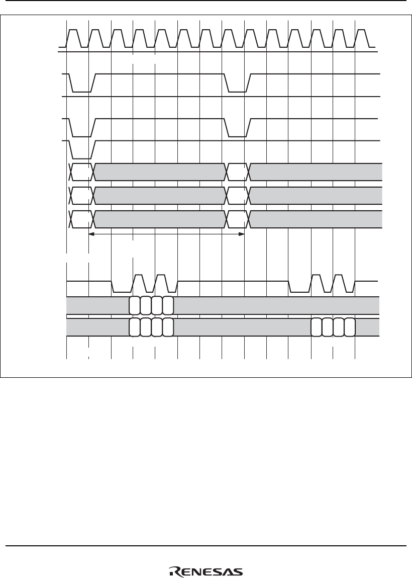
12. DDR2-SDRAM Interface (DBSC2)
Rev.1.00 Jan. 10, 2008 Page 542 of 1658
REJ09B0261-0100
MCK0,
MCK1
MA[14:11]
MA[9:0]
MBA[2:0]
MCKE
MCS
MRAS
MCAS
MWE
MA[10]
Invalid
MDQS[3:0]
MDQ[31:0]
MDM[3:0] Invalid
Invalid
Invalid
Invalid
READ
any
bank
Invalid
Invalid
Invalid
SDRAM
command
Invalid
Invalid
WRITE
any
bank
Write data Read data
WRRD
= 7 cycles
Valid
Valid
Valid
Valid
Valid
Valid
Example of CL= 3
High level
Figure 12.19 WRITE-READ Minimum Time
Figure 12.19 is an example of a case in which, after issuing a WRITE command, a READ
command is issued. In order to issue the READ command after issuing the WRITE command, the
DBSC2 waits for a minimum time stipulated by the WRRD bits.

12. DDR2-SDRAM Interface (DBSC2)
Rev.1.00 Jan. 10, 2008 Page 543 of 1658
REJ09B0261-0100
MCK0,
MCK1
MA[14:11]
MA[9:0]
MBA[2:0]
MCKE
MCS
MRAS
MCAS
MWE
MA[10]
ACT
any
bank
tRFC
Invalid
Invalid
Invalid
Invalid
MDQS[3:0]
MDQ[31:0]
MDM[3:0] Invalid
Invalid
Invalid
Invalid
REF
SDRAM
command
READ
any
bank
Invalid
Invalid
Invalid
= 6 cycles
Valid
Valid
Valid
Valid
Valid
Valid
High level
Figure 12.20 tRFC
Figure 12.20 is an example of a case in which, after issuing a REF command, a READ request is
issued. In order to issue the ACT commend after issuing the REF command, the DBSC2 waits for
a time stipulated by tRFC.

12. DDR2-SDRAM Interface (DBSC2)
Rev.1.00 Jan. 10, 2008 Page 544 of 1658
REJ09B0261-0100
12.5.8 Important Information Regarding Use of 8-Bank DDR2-SDRAM Products
The DDR2-SDRAM specifications limit the number of banks in an 8-bank product which can be
activated simultaneously. Control must be executed so that the number of activated banks never
exceeds four banks. Hence the DBSC2 handles (BA2,BA1,BA0) = (1,X,Y) and (0,X,Y) as access
to the same banks. Through this handling, no more than four banks can be activated
simultaneously. As an operation example, consider a case in which the page corresponding to
bank (BA2,BA1,BA0) = (0,0,0) is opened, and then access of (BA2,BA1,BA0) = (1,0,0) occurs.
After using a PRE command to close the page of the bank corresponding to (BA2,BA1,BA0) =
(0,0,0), the DBSC2 issues an ACT command for the bank corresponding to (BA2,BA1,BA0) =
(1,0,0) to open the page, and accesses the memory. Because the DBSC2 executes the above
control, if a program which is activated simultaneously is placed in an address area such that
(BA2,BA1,BA0) = (1,X,Y) and (0,X,Y), frequent page misses may result.
12.5.9 Important Information Regarding ODT Control Signal Output to SDRAM
The following should be noted when having the DBSC2 output an ODT control signal to the
SDRAM.
• When an ODT control signal is output to the SDRAM, a CAS latency of at least four DDR
clock cycles is necessary (figure 12.21).
• When the ODT control signal is output one DDR clock cycle early using the ODT_EARLY bit
in the DBDICODTOCD register and is extended, the CAS latency must be at least five DDR
clock cycles, and moreover the setting of the RDWR bits in the DBTR2 register must be equal
to the value required by the SDRAM specifications, plus one (figure 12.22)
The DBSC2 supports only the memory for which tAOND is two cycles and tAOFD is 2.5 cycles.

12. DDR2-SDRAM Interface (DBSC2)
Rev.1.00 Jan. 10, 2008 Page 545 of 1658
REJ09B0261-0100
write
MCK
Command
Data
MCKE
MODT
Terminating
resistor
in SDRAM
As shown in the above figure, when CL is 4, the effective ODT control signal
(MODT) to the SDRAM can be asserted at the same timing as the issue of the
WRITE command. If CL is 5 or greater, MODT is asserted after the issue of the
WRITE command. However, if CL is 3 or less, MODT needs to be asserted
before the issue of the WRITE command, which is not supported by this LSI.
Resistor ON
tAOND
= 2 cycles
3 cycles
for product
with CL = 4
High level
tAOFD
= 2.5 cycles
Figure 12.21 ODT Control Signal when CL = 4
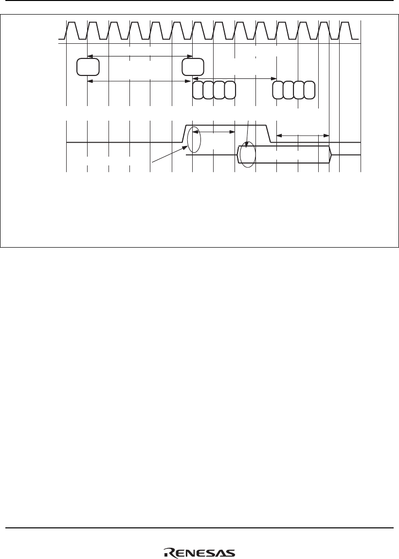
12. DDR2-SDRAM Interface (DBSC2)
Rev.1.00 Jan. 10, 2008 Page 546 of 1658
REJ09B0261-0100
write
MCK
Command
Data
MCKE
MODT
Terminating
resistor
in SDRAM
read
The above figure shows an example when a product with CL = 5 is used. As the ODT control signal (MODT)
is extended for one cycle, the product with CL = 5 or greater is required. If a product with CL = 4 or less is
used, MODT needs to be asserted before the issue of the WRITE command, which is not supported by this
LSI.
The interval between the READ and WRITE commands required for the SDRAM is assumed to be 4 cycles.
However, if the interval is 4 cycles, read data exists on the data bus when the terminating resistor in the
SDRAM is turned on since MODT is extended for one cycle. To prevent this, the interval should be set to 5
cycles.
5 cycles for
product with CL = 5
4 -> 5 cycles
tAOND
= 2 cycles
Extended for 1 cycle
tAOFD
= 2.5 cycles
If the interval from the READ command to the WRITE command is 4 cycles, read data exists
on the data bus when Rtt is turned on. Therefore, the interval should be 5 cycles.
Resistor ON
4 cycles for
product with CL = 5
High level
Figure 12.22 Important Information on One-Cycle Extension of ODT Control Signal
12.5.10 DDR2-SDRAM Power Supply Backup Function
The SDRAM power supply backup function utilizes the SDRAM self-refresh state to turn off the
power supply to most of the modules including the DBSC2 (all modules except the 1.8 V I/O),
while maintaining the data in the SDRAM. By using this function, not only is it possible to cut
power consumption, but the time needed to transfer data once again to the SDRAM can be
eliminated, since the valid data is maintained within the SDRAM (see figure 12.23). In order to
realize this function, in addition to the LSI device containing the DBSC2, a separate external
control circuit (microcomputer or similar) is needed to monitor the states of this LSI and the
memory.
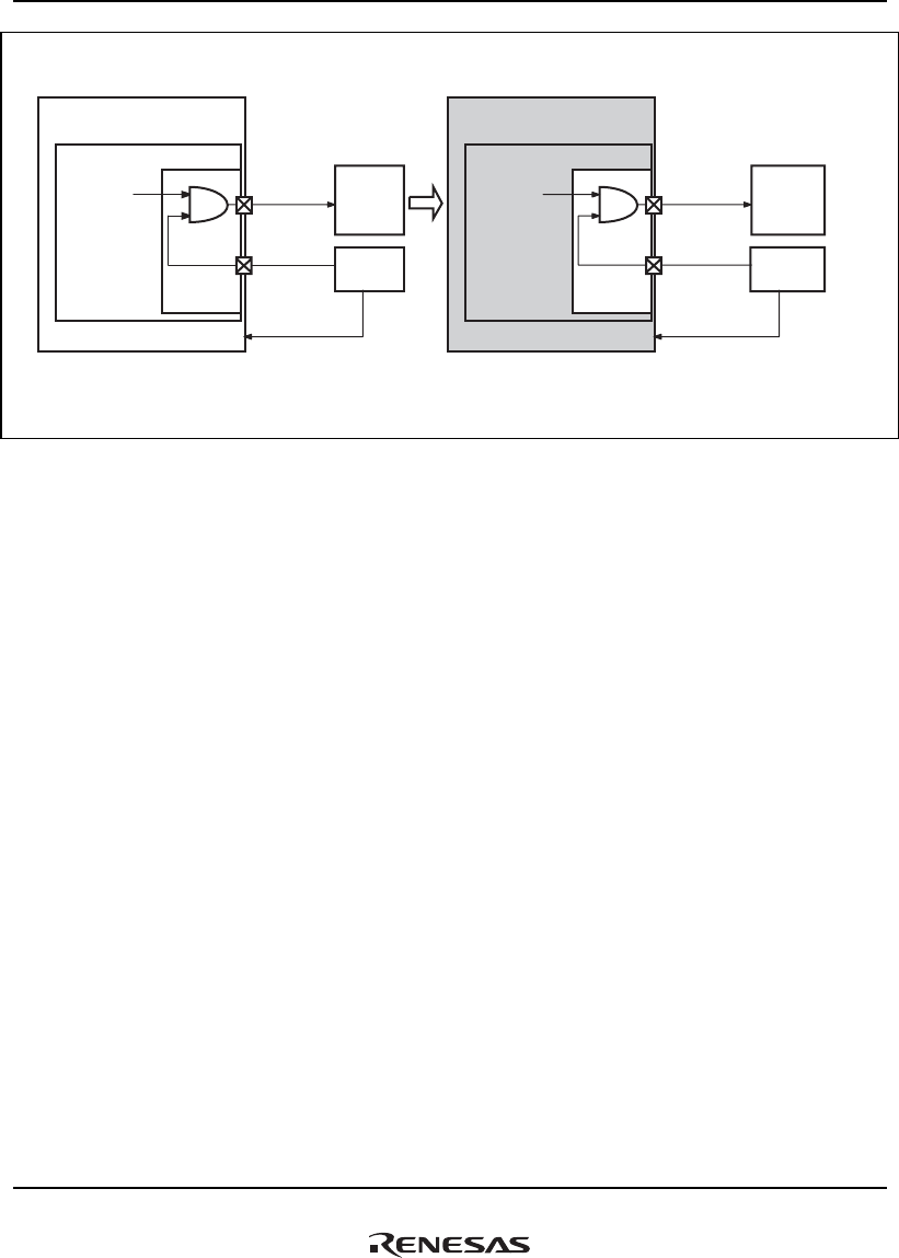
12. DDR2-SDRAM Interface (DBSC2)
Rev.1.00 Jan. 10, 2008 Page 547 of 1658
REJ09B0261-0100
This LSI
MCKE
MBKPRST
IO cell
Internal
CKE
DBSC2
External
device
SDRAM
This LSI
MCKE
MBKPRST
IO cell
Internal
CKE
DBSC2
Low level
input
Low level
output
High level
input 1.8-V
power on
1.8-V
power on
1.0-V
power on 1.0-V
power off
Normal operation When SDRAM power supply backup function is used
External
device
SDRAM
Normal
operation
Data is retained
in self-refresh state
Data
retained
Status signal Status signal
As the power to most modules, except the 1.8-V
power supply for DDRPAD, is turned off, chip
power consumption can be reduced.
Figure 12.23 SDRAM Power Supply Backup Function
In order to implement the power supply backup function, a control signal MBKPRST is necessary
to hold MCKE at low level even when power other than for the 1.8 V I/O is turned off. When this
signal is at low level, MCKE pin can be held at low level even when the power supply within the
chip is in the turned-off state. After using the DBSC2 to put the SDRAM into the self-refresh
state, by using this MBKPRST signal to hold the MCKE signal at low level, the SDRAM self-
refresh state can be maintained even when the power supply in the chip is turned off.
To cancel the power supply backup state, perform a power-on reset. As a result, the DBSC2
registers are initialized, and so the self-refresh control circuit is also initialized. In order to put the
SDRAM into the self-refresh state before power-on reset, when the internal CKE signal is
indefinite, and also during power-on reset, the MBKPRST signal must be held at low level.
Power-on reset causes the DBSC2 to fix the internal CKE signal at low level, so that after power-
on reset is released the MBKPRST signal is raised to high level. (If not in the power supply
backup state, MBKPRST is always at high level and there is no problem.)
Thus the power supply backup state is cancelled through power-on reset, and so the software must
decide whether the normal SDRAM initialization sequence is necessary, or whether the LSI was in
the power supply backup state. In order to perform this decision, a state signal is input to this LSI
from an external control circuit. The method of input is arbitrary, and a general port can be used.
After power-on reset, the software monitors the state signal applied by the external control circuit,
and judges whether the state should be the power supply backup state or whether SDRAM
initialization is necessary. Before using register settings to send MCKE to high level, the state
signal must be made to signify a state other than the power supply backup state. (After driving pin

12. DDR2-SDRAM Interface (DBSC2)
Rev.1.00 Jan. 10, 2008 Page 548 of 1658
REJ09B0261-0100
MCKE to high level, upon power-on reset the data within the SDRAM is destroyed. Hence if the
state signal is not set in advance to a state other than power supply backup state, there is the
danger that the destroyed data may be treated as the correct data.)
In this way, procedures are used to make a transition to and cancel SDRAM power supply backup
mode; if these procedures are not followed, the data in the SDRAM may be destroyed.
These procedures are explained below.
(1) Transition to SDRAM Power Supply Backup Mode
The following method is used.
1. Confirm that the controller is not being accessed. The time required for transition must not
exceed the auto-refresh interval requested by the SDRAM by interrupts or some other causes.
2. Set the ACEN bit in the SDRAM operation enable register (DBEN) to 0 (access disabled).
3. Set the ARFEN bit in the SDRAM refresh control register 0 (DBRFCNT0) to 0 (automatic
issue of auto-refresh disabled).
4. Use the CMD bits in the SDRAM command control register (DBCMDCNT) to issue a PALL
(precharge all banks) command.
5. Use the CMD bits in DBCMDCNT to issue a REF (auto-refresh) command.
6. Set the SRFEN bit in DBRFCNT0 to 1, to make a transition to self-refresh.
7. Check that the SRFEN bit is 1 by reading the SDRAM refresh control register (DBRFCNT0).
8. Use a general-purpose port or other means to convey to the external device that the SDRAM
has entered the self-refresh state. Upon receiving this notification, the external device should
change the MBKPRST signal from high level to low level.
9. Turn off the unnecessary power, other than the DBSC2 1.8 V I/O.
(2) Recovery from SDRAM Power Supply Backup Mode
The following method is used.
1. Turn on the power supply to the LSI.
2. Input a power-on reset to the LSI.
3. After release of power-on reset, an external device should change the MBKPRST signal from
low to high level.
4. An external control circuit decides, using a general-use port or the like, whether to perform a
normal initialization sequence of the SDRAM, or to recover from power supply backup mode.
For normal initialization sequence of the SDRAM, refer to section 12.5.3, Initialization
Sequence.

12. DDR2-SDRAM Interface (DBSC2)
Rev.1.00 Jan. 10, 2008 Page 549 of 1658
REJ09B0261-0100
5. The SDRAM configuration setting register (DBCONF), SDRAM timing register 0 (DBTR0),
SDRAM timing register 1 (DBTR1), and SDRAM timing register 2 (DBTR2) should be set.
6. By writing to the DDRPAD frequency setting register DBFREQ, DLL settings are made.
A. Set DLLRST = 0.
B. Set the FREQ bits to the DDRPAD frequency.
C. After setting DLLRST = 1, the software waits for the DLL stabilization time of 100 μs or
more required by DDRPAD.
7. Write to the DDRPAD DIC, ODT, OCD setting register DBDICODTOCD. Values to be
written should match values set in SDRAM EMRS(1).
8. Use the CMD bits in the SDRAM command control register (DBCMDCNT) to set the MCKE
signal to high level, and have the software wait for the time, requested by the respective
memory manufacturers, from cancellation of the self-refresh state until issue of a non-read
command (time tXSNR).
9. Write to DBCMDCNT to issue a REF (auto-refresh) command.
10. Set the ACEN bit in the SDRAM operation enable register (DBEN) to 1 (access enabled).
11. Set the SDRAM refresh control registers 1 and 2 (DBRFCNT1 and DBRFCNT2).
12. Set the ARFEN bit in the SDRAM refresh control register 0 (DBRFCNT0) to 1 (automatic
issue of auto-refresh enabled). Thereafter, normal access is possible.
12.5.11 Method for Securing Time Required for Initialization, Self-Refresh Cancellation,
etc.
When using DBSC2 register settings to set initialization, cancel self-refresh and the like, it is
necessary to wait a time stipulated by the SDRAM specifications. One example of this waiting is
the method used to read the DBSC2 status register (DBSTATE). Upon executing reading of the
DBSC2 status register (DBSTATE), a minimum of 8 cycles of the memory clock elapse. If
operation is at 300 MHz, then approximately 26 ns elapses in a single DBSTATE read operation.
This can be utilized to secure the required time, by repeating read access the necessary number of
times.
12.5.12 Regarding the Supported Clock Ratio
The only clock ratio supported by the DBSC2 is a ratio of 1:1 between the SuperHyway clock and
the DDR clock. Clock ratios other than 1:1 are not supported.
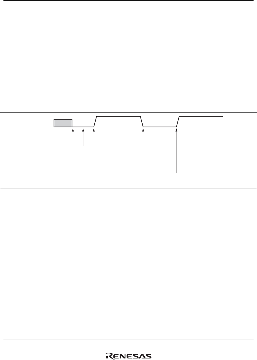
12. DDR2-SDRAM Interface (DBSC2)
Rev.1.00 Jan. 10, 2008 Page 550 of 1658
REJ09B0261-0100
12.5.13 Regarding MCKE Signal Operation
The MCKE signal operation is explained using figure 12.24. Here, the explanation assumes that
MBKPRST is high-level input. Prior to power-on reset the MCKE signal is indefinite, but upon
power-on reset is output at low level. After release of power-on reset, by writing 011 to the CMD
bits in the SDRAM command control register (DBCMDCNT), the MCKE signal output is at high
level, corresponding to the enable state. Once the MCKE signal is output at a high level in this
way, the DBSC2 does not output a low-level MCKE signal except when causing a transition to
self-refresh state. (Once the CMD bits in DBCMDCNT are set to 011, no matter what value is
subsequently written to CMD, the MCKE signal is never output at low level.) After the transition
to self-refresh state, when 0 is written to SRFEN in DBRFCNT0 to release the self-refresh state,
the MCKE signal output returns to high level.
MCKE
Undefined
Power-on reset
Power-on reset canceled
011 is written to the CMD2 to CMD0 bits
in DBCMDCNT.
The SRFEN bit in DBRFCNT0 is set to
1 (transition to self-refresh state).
The SRFEN bit in DBRFCNT0 is cleared to
0 (release of self-refresh state).
Figure 12.24 MCKE Signal Operation

13. PCI Controller (PCIC)
Rev.1.00 Jan. 10, 2008 Page 551 of 1658
REJ09B0261-0100
Section 13 PCI Controller (PCIC)
The PCI controller (PCIC) controls the PCI bus and enables data transfers between memory
connected to an external bus and a PCI device connected to the PCI bus. The PCIC facilitates the
system design using the PCI bus and enables short and fast data transfer.
The PCIC operates as a bus bridge which links the PCI bus to the internal bus (SuperHyway bus).
It has transfer channels, for example, between a PCI device on the PCI bus and memory that is
connected to the external bus.
The PCIC supports both the host mode and normal mode (non-host mode). In host mode,
arbitration can be performed on the PCI bus. In normal mode, the PCI bus arbitration is performed
by the external PCI bus arbiter.
13.1 Features
The PCIC has the following features.
• Conforms to the subset of the PCI Local Bus Specification Revision 2.2
• Operates at 33 or 66 MHz
• 32-bit data bus
• PCI master and target functions
• Conforms to the subset of the PCI Power Management Revision 1.1
• Supports the host mode and normal mode
• PCI arbiter (in host mode)
• Supports four external masters
• Pseudo-round-robin or fixed priority arbitration
• Supports external bus arbiter mode
• Supports configuration mechanism #1 (in host mode)
• Supports burst transfer
• Parity check and error report
• Exclusive access (only when PCIC is a target)
Exclusive access between the internal module and the external PCI master is not supported.
⎯ The PCIC is a master: Not supported
⎯ The PCIC is a target: When the PCIC is locked, it can be accessed through only the PCI
device that has asserted the LOCK signal (the SuperHyway bus is not locked during lock
transfer).

13. PCI Controller (PCIC)
Rev.1.00 Jan. 10, 2008 Page 552 of 1658
REJ09B0261-0100
• Cache snoop functions are supported when the PCIC is a target (cache coherency can be
supported by sacrificing performance).
• Supports four external interrupt inputs (INTA, INTB, INTC, and INTD) in host mode
• Supports one external interrupt output (INTA) in normal mode
• Both big endian and little endian are supported in SH7785 (the PCI bus operates in little
endian mode).
Note: The following PCI functions are not supported.
• Supports cache (without the SBO and SDONE pins)
• Address wraparound mechanism
• PCI JTAG (this LSI supports JTAG)
• Dual address cycles
• Interrupt acknowledge cycles
• Start of fast back-to-back transfer (it is supported when the PCIC operates as a target device)
• Extended ROM for initialization, and boot of system
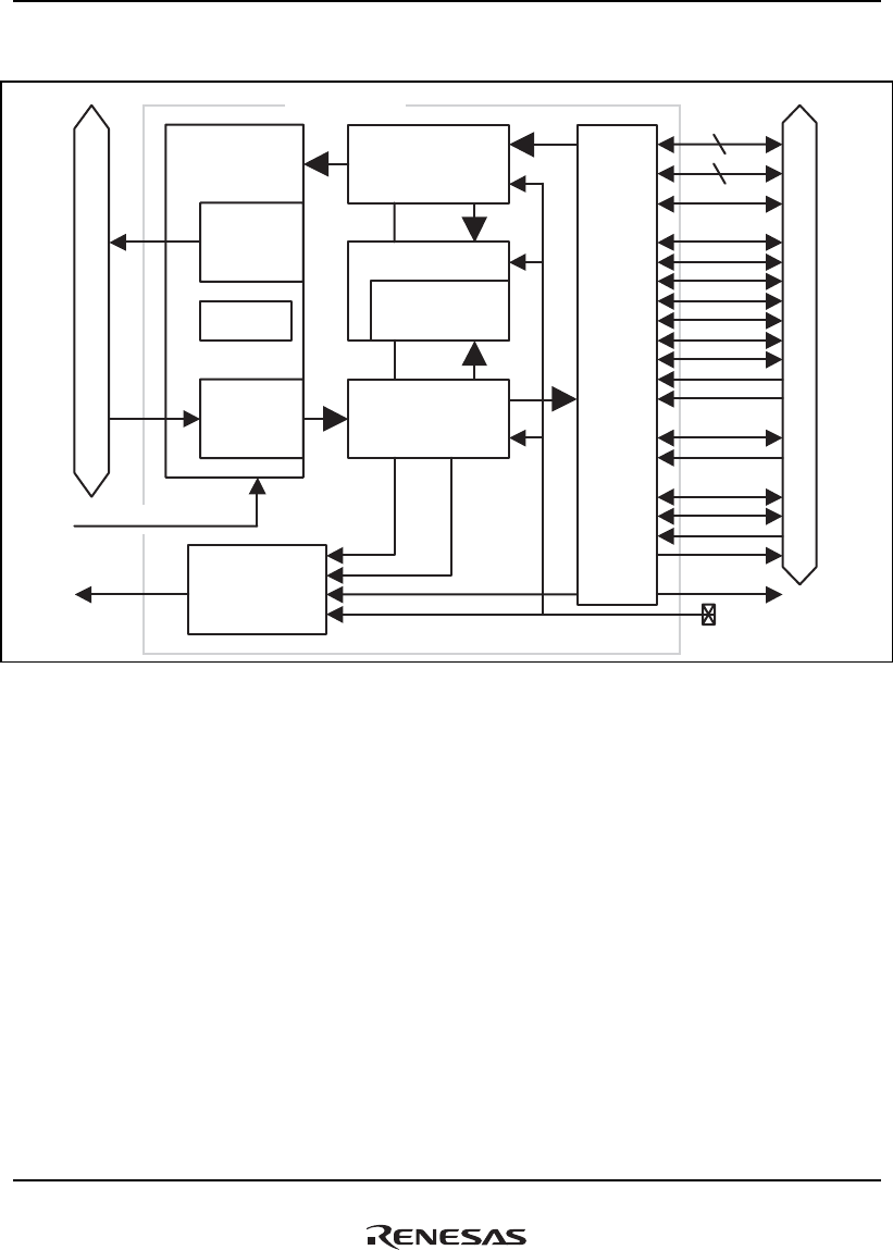
13. PCI Controller (PCIC)
Rev.1.00 Jan. 10, 2008 Page 553 of 1658
REJ09B0261-0100
Figure 13.1 shows a block diagram of the PCIC.
PCI bus
PCIC module
Internal bus (SHwybus)
SHwy bus
interface
Data FIFO
read
32 bytes x 2
PCIECR
Data FIFO
write
32 bytes x 2
SHwy clock input
Interrupt control
Interrupt
Tar get control
Register control
Configuration
registers
/local registers
Master control
PCI bus interface
(PCI bus access control)
AD[31:0]
CBE[3:0]
PAR
INTA
INT[B:D]
REQ0/REQOUT
GNT0/GNTIN
REQ[3:1]
GNT[3:1]
FRAME
IRDY
TRDY
DEVSEL
STOP
PERR
SERR
LOCK
IDSEL
PCIRESET
PCICLK input
Figure 13.1 Block Diagram of PCIC
The PCIC comprises two blocks, the PCI bus interface block and SuperHyway bus interface
block.
The PCI bus interface block comprises the PCI configuration register, local register, PCI master
controller, and PCI target controller.
The SuperHyway bus interface converts the access from the PCI bus interface into the access to
the SuperHyway bus, and converts the access from the SuperHyway bus (the CPU or DMAC) into
access to the PCI bus interface block. The SuperHyway bus interface block comprises PCIECR,
the access control block from the SuperHyway bus to the PCI bus, and the access control block
from the PCI bus to the SuperHyway bus.
The interrupt controller controls the issue of interrupts to INTC of this LSI.

13. PCI Controller (PCIC)
Rev.1.00 Jan. 10, 2008 Page 554 of 1658
REJ09B0261-0100
13.2 Input/Output Pins
Table 13.1 shows the pin configuration of the PCIC.
Table 13.1 Signal Descriptions
Signal Name
PCI Standard
Signal I/O Description
D32/AD0/DR0 to
D37/AD5/DR5,
D38/AD6/DG0 to
D43/AD11/DG5,
D44/AD12/DB0 to
D49/AD17/DB5,
D50/AD18 to
D63/AD31
AD[31:0] TRI PCI Address/Data Bus
Address and data buses are multiplexed. In each bus
transaction, an address phase is followed by one or
more data phases.
WE7/CBE3 to
WE4/CBE0
C/BE[3:0] TRI PCI Command/Byte Enable
Commands and byte enable are multiplexed. These
signals indicate the type of command and byte enable
during the address phase and the data phases
respectively.
PAR PAR TRI PCI Parity
Generates/checks even parity between AD[31:0] to
C/BE[3:0].
PCICLK/
DCLKIN
CLK IN PCI Clock
Provides timing for all transactions on the PCI bus.
PCIFRAME/
VSYNC
FRAME STRI PCI Frame
Driven by the current initiator, and indicates the start
and duration of a transaction.
TRDY/DISP TRDY STRI PCI Target Ready
Driven by the selected target, and indicates the target
is ready to start and maintain a transaction.
IRDY/HSYNC IRDY STRI PCI Initiator Ready
Driven by the current bus master. During writing,
indicates that valid data is present on the AD [31:0]
lines. During reading, indicates that the master is ready
to accept data.
STOP/CDE STOP STRI PCI Stop
Driven by the selected target drives to stop the current
transaction.

13. PCI Controller (PCIC)
Rev.1.00 Jan. 10, 2008 Page 555 of 1658
REJ09B0261-0100
Signal Name
PCI Standard
Signal I/O Description
LOCK/ODDF LOCK STRI PCI Lock
Exclusive access (the target resource is locked) is
accepted when the PCIC is a target
IDSEL IDSEL IN PCI Configuration Device Select
This signal is input to select the PCIC in configuration
cycles (only in normal mode).
DEVSEL/
DCLKOUT
DEVSEL STRI PCI Device Select
Indicates the PCIC has decoded the address of the PCI
device as the target. When this signal is an input signal,
it indicates that the PCIC has been selected.
SCIF0_CTS/
INTD
INTD IN Interrupt D
Indicates that a PCI device is requesting PCI interrupts.
Only in host mode.
DREQ3/INTC INTC IN Interrupt C
Indicates that a PCI device is requesting PCI interrupts.
Only in host mode.
DREQ2/INTB INTB IN Interrupt B
Indicates that a PCI device is requesting PCI interrupts.
Only in host mode.
INTA INTA O/D Interrupt A
Indicates that a PCI device is requesting PCI interrupts
in host mode. This signal is output so that the PCIC can
request interrupts in normal mode.
REQ3 REQ3 IN PCI Bus Request (only in host mode)
REQ2 to REQ1 REQ[2:1] IN PCI Bus Request (only in host mode)
GNT3 GNT3 TRI PCI Bus Grant (only in host mode)
GNT2 to GNT1 GNT[2:1] TRI PCI Bus Grant (only in host mode)
REQ0/REQOUT REQ0 TRI PCI Bus Request (input/output in host mode, and
output in normal mode)
GNT0/GNTIN GNT0 TRI PCI Bus Grant (output/input in host mode, and input in
normal mode)
SERR SERR O/D PCI System Error
PERR PERR TRI PCI Parity Error
PCIRESET — OUT PCI Reset Output

13. PCI Controller (PCIC)
Rev.1.00 Jan. 10, 2008 Page 556 of 1658
REJ09B0261-0100
Signal Name
PCI Standard
Signal I/O Description
MODE12
MODE11
— IN PCI Operating Mode Select
00: PCI host mode, or PCI host bridge operation by
PCICLK
01: PCI normal mode, or non-PCI host bridge operation
by PCICLK
10: Local bus 64-bit mode (the PCI disabled)
11: DU mode (the PCI disabled)
Legend:
TRI: Tri-state
STRI: Sustained tri-state
OD: Open Drain
IN: Only input
OUT: Only output

13. PCI Controller (PCIC)
Rev.1.00 Jan. 10, 2008 Page 557 of 1658
REJ09B0261-0100
13.3 Register Descriptions
Table 13.2 shows a list of PCIC registers. The addresses and offsets of PCI configuration registers
are the values used when the PCIC is in little endian mode. The access size is the maximum access
size in each register. The registers in the PCI configuration register space can be accessed with
32-, 16-, or 8-bit access sizes.
Table 13.2 List of PCIC Registers
Name Abbreviation
SH*1
R/W
PCI*2
R/W P4 address Area 7 address
Sync
Clock
Access
Size*3
Control register space (physical address: H'FE04 0000 to H'FE04 00FF)
PCIC enable control register PCIECR R/W — H'FE00 0008 H'1E00 0008 SHck 32
PCI control register space (physical address: H'FE04 0000 to H'FE04 00FF)
PCI vendor ID register PCIVID R R H'FE04 0000 H'1E04 0000 PCIclk (32)/16/8
PCI device ID register PCIDID R R H'FE04 0002 H'1E04 0002 PCIclk (32)/16/8
PCI command register PCICMD R/W R/W H'FE04 0004 H'1E04 0004 PCIclk (32)/16/8
PCI status register PCISTATUS R/W R/W H'FE04 0006 H'1E04 0006 PCIclk (32)/16/8
PCI revision ID register PCIRID R R H'FE04 0008 H'1E04 0008 PCIclk (32)/(16)/8
PCI program interface register PCIPIF R/W R H'FE04 0009 H'1E04 0009 PCIclk (32)/(16)/8
PCI sub class code register PCISUB R/W R H'FE04 000A H'1E04 000A PCIclk (32)/(16)/8
PCI base class code register PCIBCC R/W R H'FE04 000B H'1E04 000B PCIclk (32)/(16)/8
PCI cache line size register PCICLS R R H'FE04 000C H'1E04 000C PCIclk (32)/(16)/8
PCI latency timer register PCILTM R/W R/W H'FE04 000D H'1E04 000D PCIclk (32)/(16)/8
PCI header type register PCIHDR R R H'FE04 000E H'1E04 000E PCIclk (32)/(16)/8
PCI BIST register PCIBIST R R H'FE04 000F H'1E04 000F PCIclk (32)/(16)/8
PCI I/O base address register PCIIBAR R/W R/W H'FE04 0010 H'1E04 0010 PCIclk 32/16/8
PCI Memory base address
register 0
PCIMBAR0 R/W R/W H'FE04 0014 H'1E04 0014 PCIclk 32/16/8
PCI Memory base address
register 1
PCIMBAR1 R/W R/W H'FE04 0018 H'1E04 0018 PCIclk 32/16/8
PCI subsystem vendor ID
register
PCISVID R/W R H'FE04 002C H'1E04 002C PCIclk (32)/16/8
PCI subsystem ID register PCISID R/W R H'FE04 002E H'1E04 002E PCIclk (32)/16/8
PCI capabilities pointer
register
PCICP R R H'FE04 0034 H'1E04 0034 PCIclk (32)/(16)/8

13. PCI Controller (PCIC)
Rev.1.00 Jan. 10, 2008 Page 558 of 1658
REJ09B0261-0100
Name Abbreviation
SH*1
R/W
PCI*2
R/W P4 address Area 7 address
Sync
Clock
Access
Size*3
PCI interrupt line register PCIINTLINE R/W R/W H'FE04 003C H'1E04 003C PCIclk (32)/(16)/8
PCI interrupt pin register PCIINTPIN R/W R H'FE04 003D H'1E04 003D PCIclk (32)/(16)/8
PCI minimum grant register PCIMINGNT R R H'FE04 003E H'1E04 003E PCIclk (32)/(16)/8
PCI maximum latency register PCIMAXLAT R R H'FE04 003F H'1E04 003F PCIclk (32)/(16)/8
PCI capability ID register PCICID R R H'FE04 0040 H'1E04 0040 PCIclk (32)/(16)/8
PCI next item pointer register PCINIP R R H'FE04 0041 H'1E04 0041 PCIclk (32)/(16)/8
PCI power management
capability register
PCIPMC R/W R/W H'FE04 0042 H'1E04 0042 PCIclk (32)/16/8
PCI power management
control/status register
PCIPMCSR R/W R/W H'FE04 0044 H'1E04 0044 PCIclk (32)/16/8
PCI PMCSR bridge support
extension register
PCIPMCSR_
BSE
R/W R H'FE04 0046 H'1E04 0046 PCIclk (32)/(16)/8
PCI power
consumption/dissipation data
register
PCIPCDD R/W R H'FE04 0047 H'1E04 0047 PCIclk (32)/(16)/8
PCI local register space (physical address: H'FE04 0100 to H'FE04 03FF)
PCI control register PCICR R/W R H'FE04 0100 H'1E04 0100 PCIclk 32/16/8
PCI local space register 0 PCILSR0 R/W R H'FE04 0104 H'1E04 0104 PCIclk 32/16/8
PCI local space register 1 PCILSR1 R/W R H'FE04 0108 H'1E04 0108 PCIclk 32/16/8
PCI local address register 0 PCILAR0 R/W R H'FE04 010C H'1E04 010C PCIclk 32/16/8
PCI local address register 1 PCILAR1 R/W R H'FE04 0110 H'1E04 0110 PCIclk 32/16/8
PCI interrupt register PCIIR R/WC R H'FE04 0114 H'1E04 0114 PCIclk 32/16/8
PCI interrupt mask register PCIIMR R/W R H'FE04 0118 H'1E04 0118 PCIclk 32/16/8
PCI error address information
register
PCIAIR R R H'FE04 011C H'1E04 011C PCIclk 32/16/8
PCI error command
information register
PCICIR R R H'FE04 0120 H'1E04 0120 PCIclk 32/16/8
PCI arbiter interrupt register PCIAINT R/WC R H'FE04 0130 H'1E04 0130 PCIclk 32/16/8
PCI arbiter interrupt mask
register
PCIAINTM R/WC R H'FE04 0134 H'1E04 0134 PCIclk 32/16/8
PCI arbiter bus master error
information register
PCIBMIR R R H'FE04 0138 H'1E04 0138 PCIclk 32/16/8
PCI PIO address register PCIPAR R/W — H'FE04 01C0 H'1E04 01C0 PCIclk 32/16/8

13. PCI Controller (PCIC)
Rev.1.00 Jan. 10, 2008 Page 559 of 1658
REJ09B0261-0100
Name Abbreviation
SH*1
R/W
PCI*2
R/W P4 address Area 7 address
Sync
Clock
Access
Size*3
PCI power management
interrupt register
PCIPINT R/WC — H'FE04 01CC H'1E04 01CC PCIclk 32/16/8
PCI power management
interrupt mask register
PCIPINTM R/W — H'FE04 01D0 H'1E04 01D0 PCIclk 32/16/8
PCI memory bank register 0 PCIMBR0 R/W — H'FE04 01E0 H'1E04 01E0 PCIclk 32/16/8
PCI memory bank mask
register 0
PCIMBMR0 R/W — H'FE04 01E4 H'1E04 01E4 PCIclk 32/16/8
PCI memory bank register 1 PCIMBR1 R/W — H'FE04 01E8 H'1E04 01E8 PCIclk 32/16/8
PCI memory bank mask
register 1
PCIMBMR1 R/W — H'FE04 01EC H'1E04 01EC PCIclk 32/16/8
PCI memory bank register 2 PCIMBR2 R/W — H'FE04 01F0 H'1E04 01F0 PCIclk 32/16/8
PCI memory bank mask
register 2
PCIMBMR2 R/W — H'FE04 01F4 H'1E04 01F4 PCIclk 32/16/8
PCI I/O bank register PCIIOBR R/W — H'FE04 01F8 H'1E04 01F8 PCIclk 32/16/8
PCI I/O bank master register PCIIOBMR R/W — H'FE04 01FC H'1E04 01FC PCIclk 32/16/8
PCI cache snoop control
register 0
PCICSCR0 R/W — H'FE04 0210 H'1E04 0210 PCIclk 32/16/8
PCI cache snoop control
register 1
PCICSCR1 R/W — H'FE04 0214 H'1E04 0214 PCIclk 32/16/8
PCI cache snoop address
register 0
PCICSAR0 R/W — H'FE04 0218 H'1E04 0218 PCIclk 32/16/8
PCI cache snoop address
register 1
PCICSAR1 R/W — H'FE04 021C H'1E04 021C PCIclk 32/16/8
PCI PIO data register PCIPDR R/W — H'FE04 0220 H'1E04 0220 PCIclk 32/16/8
Notes: 1. SH: SuperHyway bus (internal bus)
PCI: PCI local bus
WC in R/W column: Write clear (Cleared by writing 1; writing 0 has no effect.)
⎯: Access is prohibited.
2. PIO: Programmed I/O.
3. It It is possible to access multiple registers at once by using an access size exceeding
the register size.

13. PCI Controller (PCIC)
Rev.1.00 Jan. 10, 2008 Page 560 of 1658
REJ09B0261-0100
Table 13.3 Register States in Each Processing Mode
Name Abbreviation Power-On Reset Manual Reset Sleep Mode
Control register space (physical address: H'FE00 0000 to H'FE03 FFFF)
PCIC enable control register PCIECR H'0000 0000 Retained Retained
PCI configuration register space (physical address: H'FE04 0000 to H'FE04 00FF)
PCI vendor ID register PCIVID H'1912 Retained Retained
PCI device ID register PCIDID H'0007 Retained Retained
PCI command register PCICMD H'0080 Retained Retained
PCI status register PCISTATUS H'0290 Retained Retained
PCI revision ID register PCIRID H'xx Retained Retained
PCI program interface register PCIPIF H'00 Retained Retained
PCI sub class code register PCISUB H'00 Retained Retained
PCI base class code register PCIBCC H'xx Retained Retained
PCI cache line size register PCICLS H'20 Retained Retained
PCI latency timer register PCILTM H'00 Retained Retained
PCI header type register PCIHDR H'00 Retained Retained
PCI BIST register PCIBIST H'00 Retained Retained
PCI I/O base address register PCIIBAR H'0000 0001 Retained Retained
PCI Memory base address register 0 PCIMBAR0 H'0000 0000 Retained Retained
PCI Memory base address register 1 PCIMBAR1 H'0000 0000 Retained Retained
PCI subsystem vendor ID register PCISVID H'0000 Retained Retained
PCI subsystem ID register PCISID H'0000 Retained Retained
PCI capabilities pointer register PCICP H'40 Retained Retained
PCI interrupt line register PCIINTLINE H'00 Retained Retained
PCI interrupt pin register PCIINTPIN H'01 Retained Retained
PCI minimum grant register PCIMINGNT H'00 Retained Retained
PCI maximum latency register PCIMAXLAT H'00 Retained Retained
PCI capability ID register PCICID H'01 Retained Retained
PCI next item pointer register PCINIP H'00 Retained Retained
PCI power management capability register PCIPMC H'000A Retained Retained
PCI power management control/status register PCIPMCSR H'0000 Retained Retained
PCI PMCSR bridge support extension register PCIPMCSR_
BSE
H'00 Retained Retained

13. PCI Controller (PCIC)
Rev.1.00 Jan. 10, 2008 Page 561 of 1658
REJ09B0261-0100
Name Abbreviation Power-On Reset Manual Reset Sleep Mode
PCI power consumption/dissipation data
register
PCIPCDD H'00 Retained Retained
PCI local register space (physical address: H'FE04 0100 to H'FE04 03FF)
PCI control register PCICR H'0000 00xx Retained Retained
PCI local space register 0 PCILSR0 H'0000 0000 Retained Retained
PCI local space register 1 PCILSR1 H'0000 0000 Retained Retained
PCI local address register 0 PCILAR0 H'0000 0000 Retained Retained
PCI local address register 1 PCILAR1 H'0000 0000 Retained Retained
PCI interrupt register PCIIR H'0000 0000 Retained Retained
PCI interrupt mask register PCIIMR H'0000 0000 Retained Retained
PCI error address information register PCIAIR H'xxxx xxxx Retained Retained
PCI error command information register PCICIR H'xx00 000x Retained Retained
PCI arbiter interrupt register PCIAINT H'0000 0000 Retained Retained
PCI arbiter interrupt mask register PCIAINTM H'0000 0000 Retained Retained
PCI arbiter bus master error information
register
PCIBMIR H'0000 00xx Retained Retained
PCI PIO address register PCIPAR H'80xx xxxx Retained Retained
PCI power management interrupt register PCIPINT H'0000 0000 Retained Retained
PCI power management interrupt mask
register
PCIPINTM H'0000 0000 Retained Retained
PCI memory bank register 0 PCIMBR0 H'0000 0000 Retained Retained
PCI memory bank mask register 0 PCIMBMR0 H'0000 0000 Retained Retained
PCI memory bank register 1 PCIMBR1 H'0000 0000 Retained Retained
PCI memory bank mask register 1 PCIMBMR1 H'0000 0000 Retained Retained
PCI memory bank register 2 PCIMBR2 H'0000 0000 Retained Retained
PCI memory bank mask register 2 PCIMBMR2 H'0000 0000 Retained Retained
PCI I/O bank register PCIIOBR H'0000 0000 Retained Retained
PCI I/O bank master register PCIIOBMR H'0000 0000 Retained Retained
PCI cache snoop control register 0 PCICSCR0 H'0000 0000 Retained Retained
PCI cache snoop control register 1 PCICSCR1 H'0000 0000 Retained Retained
PCI cache snoop address register 0 PCICSAR0 H'0000 0000 Retained Retained
PCI cache snoop address register 1 PCICSAR1 H'0000 0000 Retained Retained
PCI PIO data register PCIPDR H'xxxx xxxx Retained Retained

13. PCI Controller (PCIC)
Rev.1.00 Jan. 10, 2008 Page 562 of 1658
REJ09B0261-0100
13.3.1 PCIC Enable Control Register (PCIECR)
PCIECR is a register that specifies whether the PCIC is valid or invalid.
SH R/W:
PCI R/W:
SH R/W:
PCI R/W:
161718192021222324252627282931 30Bit:
Initial value:
RRRRRRRRRRRRRRRR
——————————————— —
0000000000000000
——————————————— —
R/WRRRRRRRRRRRRRRR
——————————————— —
0000000000000000
ENBL
—————————————— —
01234567891011121315 14Bit:
Initial value:
Bit Bit Name
Initial
Value R/W Description
31 to 1 — All 0 SH: R
PCI: ⎯
Reserved
These bits are always read as 0. The write value
should always be 0.
0 ENBL 0 SH: R/W
PCI: ⎯
PCI Enable Bit.
Enables (validates) the PCIC. When this bit is 0, the
PCIC is disabled and the access from the CPU to the
PCIC, or from the external PCI device to the PCIC is
invalid (the PCIECR can be accessed). The access
from other CPU is invalid during writing and undefined
during reading. The access from the external PCI
device cannot be accepted).
0: PCIC disabled
1: PCIC enabled

13. PCI Controller (PCIC)
Rev.1.00 Jan. 10, 2008 Page 563 of 1658
REJ09B0261-0100
13.3.2 Configuration Registers
The configuration registers define the programming model and usage rules of the configuration
register space in a PCI compliant device. For details, see section 6, Configuration Space, in the
PCI Local Bus Specification Revision 2.2.
(1) PCI Vender ID Register (PCIVID)
This field defines the PCI vendor ID.
01234567891011121315 14
0100100010011000
VID
RRRRRRRRRRRRRRRR
Bit:
Initial value:
SH R/W:
RRRRRRRRRRRRRRRRPCI R/W:
Bit Bit Name
Initial
Value R/W Description
15 to 0 VID H'1912 SH: R
PCI: R
PCI Vender ID
These bits indicate the vender ID that is allocated by
PCI-SIG. Renesas Technology's vendor ID is H'1912.
(2) PCI Device ID Register (PCIDID)
This field defines the PCI device ID.
01234567891011121315 14
1110000000000000
DID
RRRRRRRRRRRRRRRR
Bit:
Initial value:
SH R/W:
RRRRRRRRRRRRRRRRPCI R/W:
Bit Bit Name
Initial
Value R/W Description
15 to 0 DID H'0007 SH: R
PCI: R
PCI Device ID
These bits indicate the device ID of this LSI that is
allocated by the vendor of a PCI device.
SH7785's device ID is H'0007.

13. PCI Controller (PCIC)
Rev.1.00 Jan. 10, 2008 Page 564 of 1658
REJ09B0261-0100
(3) PCI Command Register (PCICMD)
PCICMD controls the basic functions of the PCIC to generate and respond to PCI cycles. When 0
is written to this register, this register ignores access commands from the external PCI device,
other than configuration access.
01234567891011121315 14
IOSMSBMSCMWIEVGAPSPERWCCSERREFBBE⎯⎯⎯⎯⎯⎯
0000000100000000
R/WR/WR/WRRRR/WR/WR/WRRRRRRR
Bit:
Initial value:
SH R/W:
R/WR/WR/WRRRR/WR/WR/WRRRRRRR
PCI R/W:
Bit Bit Name
Initial
Value R/W Description
15 to 10 ⎯ All 0 SH: R
PCI: R
Reserved
These bits are always read as 0. The write value
should always be 0.
9 FBBE 0 SH: R
PCI: R
PCI Fast Back-to-Back Enable
Specifies whether fast back-to-back control is
performed on the different devices or not when the
PCIC is a master.
0: Enables fast back-to-back control for the same target
1: Enables fast back-to-back control for different targets
(not supported)
8 SERRE 0 SH: R/W
PCI: R/W
SERR Output Control
Controls the SERR output.
0: SERR output disabled (pulled up by high impedance
and a pull-up resistor)
1: SERR output enabled (SERR = low output)
7 WCC 1 SH: R/W
PCI: R/W
Wait Cycle Control
Controls the address/data stepping.
When WCC is 1, both an address and data, only an
address, and only data are output at master write,
master read, and target read respectively for two clock
cycles.
0: Address/data stepping control disabled
1: Address/data stepping control enabled

13. PCI Controller (PCIC)
Rev.1.00 Jan. 10, 2008 Page 565 of 1658
REJ09B0261-0100
Bit Bit Name
Initial
Value R/W Description
6 PER 0 SH: R/W
PCI: R/W
Parity Error Response
Controls the response of the device when the PCIC
detects a parity error or receives a parity error. When
this bit is set to 1, the PERR signal is asserted.
0: Ignores parity error
1: Responds to parity error
5 VGAPS 0 SH: R
PCI: R
VGA Palette Snoop Control
0: VGA compatible device
1: Incompatible with palette register write (not
supported)
4 MWIE 0 SH: R
PCI: R
Memory Write and Invalidate Control
This bit controls issue of a memory and invalidate
command when the PCIC is a master.
0: Memory write is used
1: Memory write and invalidate command can be
executed (not supported)
3 SC 0 SH: R
PCI: R
Special Cycle Control
This bit indicates whether special cycles are supported
when the PCIC is a target.
0: Special cycles ignored
1: Special cycles monitored (not supported)
2 BM 0 SH: R/W
PCI: R/W
PCI Bus Master Control
Controls a bus master.
0: Bus master disabled
1: Bus master enabled
1 MS 0 SH: R/W
PCI: R/W
PCI Memory Space Control
This bit controls accesses to memory spaces when the
PCIC is a target. When this bit is cleared to 0, a
memory transfer to the PCIC is completed by master
abort.
0: Accesses to memory spaces disabled
1: Accesses to memory spaces enabled
0 IOS 0 SH: R/W
PCI: R/W
PCI I/O Space Control
This bit controls accesses to memory spaces when the
PCIC is a target. When this bit is cleared to 0, an I/O
transfer to the PCIC is completed by master abort.
0: Accesses to I/O spaces disabled
1: Accesses to I/O spaces enabled

13. PCI Controller (PCIC)
Rev.1.00 Jan. 10, 2008 Page 566 of 1658
REJ09B0261-0100
(4) PCI Status Register (PCISTATUS)
PCISTATUS is used to record status information for events related to the PCI bus. The reserved
bits are read-only bits that are read as 0.
Reading from this register is normally performed. During writing, the write clear bit can be reset,
but it cannot be set (R/WC in the figure below). Write 1 to the bit to be cleared. For example, to
clear bit 14 so that other bits will not be affected, write the B'0100 0000 0000 0000 to this register.
01234567891011121315 14
⎯⎯⎯⎯
CL66C⎯FBBCMDPEDEVSELSTARTARMADPE SSE
0000100101000000
RRRRRR/WRRR/WCRRR/WCR/WCR/WCR/WC R/WC
Bit:
Initial value:
SH R/W:
RRRRRRRRR/WCRRR/WCR/WCR/WCR/WC R/WC
PCI R/W:
Bit Bit Name
Initial
Value R/W Description
15 DPE 0 SH: R/WC
PCI: R/WC
Parity Error Detect Status
Indicates that a parity error was detected in read data
when the PCIC is a master, or in write data when the
PCIC is a target. This bit is set regardless of the value
of parity error response bit.
0: Device did not detect parity error.
1: Device detected parity error.
14 SSE 0 SH: R/WC
PCI: R/WC
System Error Output Status
Indicates that the PCIC asserted SERR.
0: SERR was asserted
1: SERR was asserted (the value is retained until this
bit is cleared)
13 RMA 0 SH: R/WC
PCI: R/WC
Master Abort Receive Status
This bit indicates that a transaction was completed by
master abort when the PCIC is a master.
0: Transaction is not completed by master abort
1: The bus master detected completion of transaction
by master abort. Master abort is not set in special
cycles.

13. PCI Controller (PCIC)
Rev.1.00 Jan. 10, 2008 Page 567 of 1658
REJ09B0261-0100
Bit Bit Name
Initial
Value R/W Description
12 RTA 0 SH: R/WC
PCI: R/WC
Target Abort Receive Status
This bit indicates that a transaction was completed by
target abort when the PCIC is a master.
0: Transaction is not completed with target abort
1: The bus master detected completion of transaction
with target abort.
11 STA 0 SH: R/WC
PCI: R/WC
Target Abort Execution Status
This bit indicates that a transaction was completed by
target abort when the PCIC is a target.
0: Transaction is not completed by target abort
1: Transaction was completed by target abort
10, 9 DEVSEL 01 SH: R
PCI: R
DEVSEL Timing Status
This bit indicate the response timing status of
DEVSEL when the PCIC is a target.
00: Fast (not support)
01: Medium
10: Slow (not support)
11: Reserved
8 MDPE 0 SH: R/WC
PCI: R/WC
Data Parity Error
This bit indicates that the PCIC asserted PERR or
detected the assertion of PERR when the PCIC is a
master. This bit is set to 1 only when the parity
response bit is set to 1.
0: Data parity error is not generated
1: Data parity error was generated
7 FBBC 1 SH: R
PCI: R
Fast Back-to-Back Status
This bit indicates whether a target can accept fast
back-to-back transfers for a different target if the PCIC
is a target.
0: A target does not support fast back-to-back
transactions for a different target
1: A target supports fast back-to-back transactions for
a different target

13. PCI Controller (PCIC)
Rev.1.00 Jan. 10, 2008 Page 568 of 1658
REJ09B0261-0100
Bit Bit Name
Initial
Value R/W Description
6 ⎯ 0 SH: R/W
PCI: R
Reserved
These bits are always read as 0. The write value
should always be 0.
5 66C 0 SH: R/W
PCI: R
66MHz-Operation Capable Status
Indicates whether the PCIC can operate at 66MHz.
0: PCIC operates at 33 MHz
1: PCIC operates at 66 MHz
4 CL 1 SH: R
PCI: R
PCI Power Management (extended function)
Indicates whether the PCI power management is
supported.
0: Power management not supported
1: Power management supported
3 to 0 ⎯ All 0 SH: R
PCI: R
Reserved
These bits are always read as 0. The write value
should always be 0.
(5) PCI Revision ID Register (PCIRID)
PCIRID specifies a revision identifier specific to a PCI device.
01234567
xxxxxxxx
RID
RRRRRRRR
Bit:
Initial value:
SH R/W:
RRRRRRRRPCI R/W:
Bit Bit Name
Initial
Value R/W Description
7 to 0 RID H'xx SH: R
PCI: R
Revision ID
Indicates the level revision of the PCIC.The initial
value depends on the logic version of this LSI.

13. PCI Controller (PCIC)
Rev.1.00 Jan. 10, 2008 Page 569 of 1658
REJ09B0261-0100
(6) PCI Program Interface Register (PCIPIF)
This field is the programming interface for the class code of the IDE controller. For details of the
code value, see appendix D in PCI Local Bus Specification Revision 2.2.
RRRRRRRRPCI R/W:
01234567
00000000
OMPPIPOMSPIS———
MIDED
R/WR/WR/WR/WRRRR/W
Bit:
Initial value:
SH R/W:
Bit Bit Name
Initial
Value R/W Description
7 MIDED 0 SH: R/W
PCI: R
PCI Master IDE Device
Specifies the PCI master IDE device.
0: PCI slave IDE device
1: PCI master IDE device
If this bit is written during register initialization
(PCICR.CFINT = 0) in the PCIC, the value of this bit is
updated. The value is not updated after initialization
(PCICR.CFINT = 1).
6 to 4 ⎯ All 0 SH: R
PCI: R
Reserved
These bits are always read as 0. The write value
should always be 0.
3 PIS 0 SH: R/W
PCI: R
PCI Programmable Indicator (Secondary)
If this bit is written during register initialization
(PCICR.CFINT = 0) in the PCIC, the value of this bit is
updated. The value is not updated after initialization
(PCICR.CFINT = 1).
2 OMS 0 SH: R/W
PCI: R
PCI Operating Mode (Secondary)
If this bit is written during register initialization
(PCICR.CFINT = 0) in the PCIC, the value of this bit is
updated. The value is not updated after initialization
(PCICR.CFINT = 1).
1 PIP 0 SH: R/W
PCI: R
PCI Programmable Indicator (Primary)
If this bit is written during register initialization
(PCICR.CFINT = 0) in the PCIC, the value of this bit is
updated. The value is not updated after initialization
(PCICR.CFINT = 1).

13. PCI Controller (PCIC)
Rev.1.00 Jan. 10, 2008 Page 570 of 1658
REJ09B0261-0100
Bit Bit Name
Initial
Value R/W Description
0 OMP 0 SH: R/W
PCI: R
PCI Operating Mode (Primary)
If this bit is written during register initialization
(PCICR.CFINT = 0) in the PCIC, the value of this bit is
updated. The value is not updated after initialization
(PCICR.CFINT = 1).
(7) PCI Sub Class Code Register (PCISUB)
This field defines the sub class code. For details of the code value, see appendix D in PCI Local
Bus Specification Revision 2.2.
01234567
00000000
SUB
R/WR/WR/WR/WR/WR/WR/WR/W
Bit:
Initial value:
SH R/W:
RRRRRRRRPCI R/W:
Bit Bit Name
Initial
Value R/W Description
7 to 0 SUB H'00 SH: R/W
PCI: R
Sub Class Code
These bits indicate the sub class code. The initial
value is H'00.

13. PCI Controller (PCIC)
Rev.1.00 Jan. 10, 2008 Page 571 of 1658
REJ09B0261-0100
(8) PCI Base Class Code Register (PCIBCC)
This field defines the base class code. For details of the class code, see appendix D in PCI Local
Bus Specification Revision 2.2.
01234567
xxxxxxxx
BCC
R/WR/WR/WR/WR/WR/WR/WR/W
Bit:
Initial value:
SH R/W:
RRRRRRRRPCI R/W:
Bit Bit Name
Initial
Value R/W Description
7 to 0 BCC H'xx SH: R/W
PCI: R
Base Class Code
These bits indicate the base class code. The initial
value is H'xx.
(9) PCI Cache Line Size Register (PCICLS)
01234567
00000100
CLS
RRRRRRRR
Bit:
Initial value:
SH R/W:
RRRRRRRRPCI R/W:
Bit Bit Name
Initial
Value R/W Description
7 to 0 CLS H'20 SH: R
PCI: R
Cache Line Size
SBO and SDON are ignored because a memory
target does not support cache.

13. PCI Controller (PCIC)
Rev.1.00 Jan. 10, 2008 Page 572 of 1658
REJ09B0261-0100
(10) PCI Latency Timer Register (PCILTM)
01234567
00000000
LTM
R/WR/WR/WR/WR/WR/WR/WR/W
Bit:
Initial value:
SH R/W:
R/WR/WR/WR/WR/WR/WR/WR/WPCI R/W:
Bit Bit Name
Initial
Value R/W Description
7 to 0 LTM H'00 SH: R/W
PCI: R/W
Latency Timer Register
These bits specify the maximum time that the PCI bus
is occupied with the clock cycle when the PCIC is a
master.
(11) PCI Header Type Register (PCIHDR)
RRRRRRRRPCI R/W:
01234567
00000000
HDR
MFE
RRRRRRRR
Bit:
Initial value:
SH R/W:
Bit Bit Name
Initial
Value R/W Description
7 MFE 0 SH: R
PCI: R
Multiple Function Enable (HEAD7)
Indicates whether the device is multi-function or
single-function
0: Single function device
1: The device has two to eight multifunction devices
(not supported)
6 to 0 HDR H'00 SH: R
PCI: R
Configuration Layout Type (HEAD6 to HEAD0)
These bits indicate the layout type of configuration
registers.
H'00: Type 00h layout supported
H'01: Type 01h layout supported (not supported)

13. PCI Controller (PCIC)
Rev.1.00 Jan. 10, 2008 Page 573 of 1658
REJ09B0261-0100
(12) PCI BIST Register (PCIBIST)
RRRRRRRRPCI R/W:
01234567
00000000
———————
BISTC
RRRRRRRR
Bit:
Initial value:
SH R/W:
Bit Bit Name
Initial
Value R/W Description
7 BISTC 0 SH: R
PCI: R
This bit is used for the BIST function control and
status.
0: Function not available
1: Function available (not supported)
6 to 0 ⎯ All 0 SH: R
PCI: R
Reserved
These bits are always read as 0. The write value
should always be 0.
13. PCI Controller (PCIC)
Rev.1.00 Jan. 10, 2008 Page 574 of 1658
REJ09B0261-0100
(13) PCI I/O Base Address Register (PCIIBAR)
This register is the I/O space base address register of the PCI configuration register space header
that is defined in PCI local bus specification. This register specifies the base address in the I/O
space of the PCIC.
See section 13.4.4 (2), Accessing PCIC I/O Space.
01234567891011121315 14
ASI
⎯IOB2 (lower)IOB1 (upper)
1000000000000000
RRRRRRRRR/WR/WR/WR/WR/WR/WR/W R/W
Bit:
Initial value:
SH R/W:
RRRRRRRRR/WR/WR/WR/WR/WR/WR/W R/W
PCI R/W:
161718192021222324252627282931 30
IOB1 (upper)
0000000000000000
R/WR/WR/WR/WR/WR/WR/WR/WR/WR/WR/WR/WR/WR/WR/W R/W
Bit:
Initial value:
SH R/W:
R/WR/WR/WR/WR/WR/WR/WR/WR/WR/WR/WR/WR/WR/WR/W R/WPCI R/W:
Bit Bit Name
Initial
Value R/W Description
31 to 8 IOB1
(upper)
H'000000 SH: R/W
PCI: R/W
I/O Space Base Address (upper 24 bits)
These bits specify the upper 24 bits of the base
address for the I/O space of the PCIC (PCIC control
register space).
7 to 2 IOB2
(lower)
000000 SH: R
PCI: R
I/O Space Base Address (lower 6 bits)
These bits are fixed to B'000000 by hardware.
1 ⎯ 0 SH: R
PCI: R
Reserved
This bit is always read as 0. The write value should
always be 0.
0 ASI 1 SH: R
PCI: R
Address Space Indicator
Indicates whether the base address indicated by this
register is in the I/O space or memory space.
0: Memory space
1: I/O space

13. PCI Controller (PCIC)
Rev.1.00 Jan. 10, 2008 Page 575 of 1658
REJ09B0261-0100
(14) PCI Memory Base Address Register 0 (PCIMBAR0)
This register is the memory base address register of the PCI configuration register space header
that is defined in PCI local bus specification. PCIMBAR0 specifies the memory space 0 (local
address space 0) in this LSI internal bus (SuperHyway bus).
See section 13.4.4 (1), Accessing Memory Space in This LSI.
01234567891011121315 14
ASILATLAPMBA2
0000000000000000
RRRRRRRRRRRRRRRR
Bit:
Initial value:
SH R/W:
RRRRRRRRRRRRRRRR
PCI R/W:
161718192021222324252627282931 30
MBA1 MBA2
0000000000000000
RRRRR/WR/WR/WR/WR/WR/WR/WR/WR/WR/WR/W R/W
Bit:
Initial value:
SH R/W:
RRRRR/WR/WR/WR/WR/WR/WR/WR/WR/WR/WR/W R/W
PCI R/W:
Bit Bit Name
Initial
Value R/W Description
31 to 20 MBA1 H'000 SH: R/W
PCI: R/W
Memory Space 0 Base Address (upper 12 bits)
These bits specify the upper 12 bits of memory base
address for the local address space 0 (the address
space in the internal bus).
The valid bits of MBA1 depend on the capacity of the
local address space specified with LSR in PCILSR0.
LSR in PCILSR0 Address space Valid bits of MBA1
[28:20]
B'0 0000 0000 1 Mbyte [31:20]
B'0 0000 0001 2 Mbytes [31:21]
B'0 0000 0011 4 Mbytes [31:22]
B'0 0000 0111 8 Mbytes [31:23]
B'0 0000 1111 16 Mbytes [31:24]
B'0 0001 1111 32 Mbytes [31:25]
B'0 0011 1111 64 Mbytes [31:26]
B'0 0111 1111 128 Mbytes [31:27]
B'0 1111 1111 256 Mbytes [31:28]
B'1 1111 1111 512 Mbytes [31:29]
Other than above: Setting prohibited

13. PCI Controller (PCIC)
Rev.1.00 Jan. 10, 2008 Page 576 of 1658
REJ09B0261-0100
Bit Bit Name
Initial
Value R/W Description
19 to 4 MBA2 H'0000 SH: R
PCI: R
Memory Space 0 Base Address (lower 16 bits)
These bits are fixed to H'0000 by hardware.
3 LAP 0 SH: R
PCI: R
Prefetch Control
Indicates whether prefetch can be performed in local
address space 0.
0: Prefetch disabled
1: Prefetch enabled (not supported)
2, 1 LAT 00 SH: R
PCI: R
Memory Type
These bits indicate the memory type of local address
space 0.
00: Base address can be set to 32-bit width and 32-bit
space
01: Reserved
10: Base address is set to 64-bit width (Not
supported)
11: Reserved
0 ASI 0 SH: R
PCI: R
Address Space Indicator
Indicates whether the base address indicated by this
register is in the I/O space or memory space.
0: Memory space
1: I/O space
13. PCI Controller (PCIC)
Rev.1.00 Jan. 10, 2008 Page 577 of 1658
REJ09B0261-0100
(15) PCI Memory Base Address Register 1 (PCIMBAR1)
This register is the memory base address register of the PCI configuration register space header
that is defined in PCI local bus specification. PCIMBAR1 specifies the memory space 1 (local
address space 1) in this LSI internal bus (SuperHyway bus).
See section 13.4.4 (1), Accessing Memory Space in This LSI.
01234567891011121315 14
ASILATLAPMBA2
0000000000000000
RRRRRRRRRRRRRRRR
Bit:
Initial value:
SH R/W:
RRRRRRRRRRRRRRRR
PCI R/W:
161718192021222324252627282931 30
MBA1 MBA2
0000000000000000
RRRRR/WR/WR/WR/WR/WR/WR/WR/WR/WR/WR/W R/W
Bit:
Initial value:
SH R/W:
RRRRR/WR/WR/WR/WR/WR/WR/WR/WR/WR/WR/W R/W
PCI R/W:
Bit Bit Name
Initial
Value R/W Description
31 to 20 MBA1 H'000 SH: R/W
PCI: R/W
Memory Space 1 Base Address (upper 12 bits)
These bits specify the upper 12 bits of memory base
address for the local address space 1 (the address
space in the internal bus).
The valid bits of MBA1 depend on the capacity of the
local address space specified with LSR in PCILSR1.
LSR Address space Valid bits of
in PCILSR1 MBA1
[28:20]
B'0 0000 0000 1 Mbyte [31:20]
B'0 0000 0001 2 Mbytes [31:21]
B'0 0000 0011 4 Mbytes [31:22]
B'0 0000 0111 8 Mbytes [31:23]
B'0 0000 1111 16 Mbytes [31:24]
B'0 0001 1111 32 Mbytes [31:25]
B'0 0011 1111 64 Mbytes [31:26]
B'0 0111 1111 128 Mbytes [31:27]
B'0 1111 1111 256 Mbytes [31:28]
B'1 1111 1111 512 Mbytes [31:29]
Other than above: Setting prohibited

13. PCI Controller (PCIC)
Rev.1.00 Jan. 10, 2008 Page 578 of 1658
REJ09B0261-0100
Bit Bit Name
Initial
Value R/W Description
19 to 4 MBA2 H'0000 SH: R
PCI: R
Memory Space 1 Base Address (lower 16 bits)
These bits are fixed to H'0000 by hardware.
3 LAP 0 SH: R
PCI: R
Prefetch Control
Indicates whether prefetch can be performed in local
address space 1.
0: Prefetch disabled
1: Prefetch enabled (not supported)
2, 1 LAT 00 SH: R
PCI: R
Memory Type
These bits indicate the memory type of local address
space 1.
00: Base address can be set to 32-bit width and 32-bit
space
01: Reserved
10: Base address is set to 64-bit width (Not
supported)
11: Reserved
0 ASI 0 SH: R
PCI: R
Address Space Indicator
Indicates whether the base address indicated by this
register is in the I/O or memory space.
0: Memory space
1: I/O space

13. PCI Controller (PCIC)
Rev.1.00 Jan. 10, 2008 Page 579 of 1658
REJ09B0261-0100
(16) PCI Subsystem Vender ID Register (PCISVID)
See the description of each register in PCI Local Bus Specification Revision 2.2.
01234567891011121315 14
SVID
0000000000000000
R/WR/WR/WR/WR/WR/WR/WR/WR/WR/WR/WR/WR/WR/WR/W R/W
Bit:
Initial value:
SH R/W:
RRRRRRRRRRRRRRRRPCI R/W:
Bit Bit Name
Initial
Value R/W Description
15 to 0 SVID H'0000 SH: R/W
PCI: R
Subsystem ID
These bits specify the subsystem ID of the PCIC.
These bits are updated when these bits are written
during the initialization (CFINIT = 0 in PCICR) in the
PCIC. The value is not updated when these bits are
written after initialization (CFINIT = 1 in PCICR).
(17) PCI Subsystem ID Register (PCISID)
See description of each register in PCI Local Bus Specification Revision 2.2.
01234567891011121315 14
SID
0000000000000000
R/WR/WR/WR/WR/WR/WR/WR/WR/WR/WR/WR/WR/WR/WR/W R/W
Bit:
Initial value:
SH R/W:
RRRRRRRRRRRRRRRRPCI R/W:
Bit Bit Name
Initial
Value R/W Description
15 to 0 SID H'0000 SH: R/W
PCI: R
Subsystem Vendor ID
These bits specify the subsystem vendor ID of the
PCIC.
These bits are updated when these bits are written
during the initialization (CFINIT = 0 in PCICR) in the
PCIC. The value is not updated when these bits are
written after initialization (CFINIT = 1 in PCICR).

13. PCI Controller (PCIC)
Rev.1.00 Jan. 10, 2008 Page 580 of 1658
REJ09B0261-0100
(18) PCI Capability Pointer Register (PCICP)
This register is the extension function pointer register of the PCI configuration register that is
defined in the PCI Power Management Specification.
01234567
00000010
CP
RRRRRRRR
Bit:
Initial value:
SH R/W:
RRRRRRRRPCI R/W:
Bit Bit Name
Initial
Value R/W Description
7 to 0 CP H'40 SH: R
PCI: R
Capabilities Pointer
These bits indicate the offset of the expansion
function (power management) ID register.
(19) PCI Interrupt Line Register (PCIINTLINE)
01234567
00000000
INTLINE
R/WR/WR/WR/WR/WR/WR/WR/W
Bit:
Initial value:
SH R/W:
R/WR/WR/WR/WR/WR/WR/WR/WPCI R/W:
Bit Bit Name
Initial
Value R/W Description
7 to 0 INTLINE H'00 SH: R/W
PCI: R/W
PCI Interrupt Line
These bits specify the information on PCI interrupt
path from this LSI. These bits are set by system
software during initialization. The initial value is H'00.
The setting value of this register does not affect the
operation of this LSI.

13. PCI Controller (PCIC)
Rev.1.00 Jan. 10, 2008 Page 581 of 1658
REJ09B0261-0100
(20) PCI Interrupt Pin Register (PCIINTPIN)
01234567
10000000
INTPIN
R/WR/WR/WR/WR/WR/WR/WR/W
Bit:
Initial value:
SH R/W:
RRRRRRRRPCI R/W:
Bit Bit Name
Initial
Value R/W Description
7 to 0 INTPIN H'01 SH: R/W
PCI: R
Interrupt Pin Select
These bits specify which interrupt pin is used as
connection destination when the PCIC outputs
interrupt requests. The initial value is H'01.
H'00: PCI interrupt pins not used
H'01: INTA used
H'02: INTB used
H'03: INTC used
H'04: INTD used
H'05 to H'FF: Reserved
(21) Minimum Grant Register (PCIMINGNT)
This register is not programmable.
01234567
00000000
MINGNT
RRRRRRRR
Bit:
Initial value:
SH R/W:
RRRRRRRRPCI R/W:
Bit Bit Name
Initial
Value R/W Description
7 to 0 MINGNT H'00 SH: R
PCI: R
Minimum Grant Specification
These bits specify the burst time required by the PCI
master device (not supported).

13. PCI Controller (PCIC)
Rev.1.00 Jan. 10, 2008 Page 582 of 1658
REJ09B0261-0100
(22) Maximum Latency Register (PCIMAXLAT)
This register is not programmable.
01234567
00000000
MAXLAT
RRRRRRRR
Bit:
Initial value:
SH R/W:
RRRRRRRRPCI R/W:
Bit Bit Name
Initial
Value R/W Description
7 to 0 MAXLAT H'00 SH: R
PCI: R
Maximum Latency Specification (MILAT7 to MILAT0)
These bits specify the maximum time from requesting
the bus mastership by the PCI master device to
acquiring bus (not supported).
(23) PCI Capability Identifier Register (PCICID)
01234567
10000000
CID
RRRRRRRR
Bit:
Initial value:
SH R/W:
RRRRRRRRPCI R/W:
Bit Bit Name
Initial
Value R/W Description
7 to 0 CID H'01 SH: R
PCI: R
Extension Function ID
These bits specify the extension function ID.
H'01: Indicates that the expansion function is power
management.

13. PCI Controller (PCIC)
Rev.1.00 Jan. 10, 2008 Page 583 of 1658
REJ09B0261-0100
(24) PCI Next Item Pointer Register (PCINIP)
PCINIP indicates the location of the next item in the list of extension function.
01234567
00000000
NIP
RRRRRRRR
Bit:
Initial value:
SH R/W:
RRRRRRRRPCI R/W:
Bit Bit Name
Initial
Value R/W Description
7 to 0 NIP H'00 SH: R
PCI: R
Next Item Pointer
H'00: Indicates that power management function is
listed as the last item.

13. PCI Controller (PCIC)
Rev.1.00 Jan. 10, 2008 Page 584 of 1658
REJ09B0261-0100
(25) PCI Power Management Register (PCIPMC)
PCIPMC is a 16-bit register that provides information on the functions related to power
management. For details, see section 3, PCI Power Management Interface in PCI Bus Power
Management Interface Specification Revision 1.1. This register is not cleared by a power-on reset.
This register must be set during initialization of register initialization in the PCIC (CFINIT = 0 in
PCICR).
01234567891011121315 14
PMVPMEC⎯DSI⎯⎯⎯D1SD2SPMCS
0101000000000000
R/WR/WR/WR/WRRRRRR/WR/WRRRRR
Bit:
Initial value:
SH R/W:
RRRRRRRRRRRRRRRR
PCI R/W:
Bit Bit Name
Initial
Value R/W Description
15 to 11 PMCS 00000 SH: R
PCI: R
PME SUPPORT
This 5-bit field indicates the power state that asserts
PME, by using this power management function.
When these bits are 0, these bits indicate that this
function cannot assert PME at that power state (not
supported).
(Bit11) xxxx1: PME can be asserted from D0
(Bit12) xxx1x: PME can be asserted from D1
(Bit13) xx1xx: PME can be asserted from D2
(Bit14) x1xxx: PME can be asserted from D3hot
(Bit15) 1xxxx: PME can be asserted from D3cold
Note: The PCIC in this LSI dose not have the PME
pin.
10 D2S 0 SH: R/W
PCI: R
D2 Support
When this bit is 1, this power management function
supports the D2 power management state. When the
D2 power management state is not supported, this bit
should always be read as 0.
9 D1S 0 SH: R/W
PCI: R
D1 Support
When this bit is 1, This function supports the D1
power management state. When the D1 power
management state is not supported, this bit is read as
0.

13. PCI Controller (PCIC)
Rev.1.00 Jan. 10, 2008 Page 585 of 1658
REJ09B0261-0100
Bit Bit Name
Initial
Value R/W Description
8 to 6 ⎯ All 0 SH: R
PCI: R
Reserved
These bits are always read as 0. The write value
should always be 0.
5 DSI 0 SH: R
PCI: R
DSI
The write value should always be 0.
0: Indicates that the proper initialization is not required
4 ⎯ 0 SH: R
PCI: R
Reserved
These bits are always read as 0. The write value
should always be 0.
3 PMEC 1 SH: R/W
PCI: R
PCI PME Clock
Specifies whether the clock is required to support
PME.
0: The clock is not required to support PME.
Note: The PCIC in this LSI dose not have the PME
pin.
2 to 0 PMV 010 SH: R/W
PCI: R
Version
Indicates the version of the power management
specifications.
010: Indicates that the power management
specification conforms to revision 1.1

13. PCI Controller (PCIC)
Rev.1.00 Jan. 10, 2008 Page 586 of 1658
REJ09B0261-0100
(26) PCI Power Management Control/Status Register (PCIPMCSR)
This register manages power management events (PME) of the PCI function. For details, see
section 3, PCI Power Management Interface in PCI Bus Power Management Interface
Specification Revision 1.1.
01234567891011121315 14
PS⎯⎯⎯⎯⎯⎯
PME
EN
DSLDSCPMES
0000000000000000
R/WR/WRRRRRRRRRRRRRR
Bit:
Initial value:
SH R/W:
R/WR/WRRRRRRRRRRRRRR
PCI R/W:
Bit Bit Name
Initial
Value R/W Description
15 PMES 0 SH: R
PCI: R
PME Status
Indicates the state of the PME signal (not supported)
Note: The PCIC in this LSI dose not has the PME
pin.
14, 13 DSC 00 SH: R
PCI: R
Data Scale
These bits specify the scaling value of data field (not
supported)
12 to 9 DSL 0000 SH: R
PCI: R
Data Select
These bits specify the value output to the data field
(not supported)
8 PMEEN 0 SH: R
PCI: R
PME Enable
Controls the PME output (not supported)
Note: The PCIC in this LSI dose not has the PME
pin.
7 to 2 ⎯ All 0 SH: R
PCI: R
Reserved
These bits are always read as 0. The write value
should always be 0.

13. PCI Controller (PCIC)
Rev.1.00 Jan. 10, 2008 Page 587 of 1658
REJ09B0261-0100
Bit Bit Name
Initial
Value R/W Description
1, 0 PS 00 SH: R/W
PCI: R/W
Power State
These bits specify the power state.
If an unsupported state is specified, a state transition
is not made. However, the register is written normally
and no error is indicated.
00: D0 state
01: D1 state
10: D2 state
11: D3 hot state

13. PCI Controller (PCIC)
Rev.1.00 Jan. 10, 2008 Page 588 of 1658
REJ09B0261-0100
(27) PCIPMCSR Bridge Support Extension Register (PCIPMCSRBSE)
This register supports the functions specific to the PCI bridge and is required for all PCI-to-PCI
bridges.
01234567
00000000
——————
B2B3N
BPC
CEN
RRRRRRRR
Bit:
Initial value:
SH R/W:
RRRRRRRR
PCI R/W:
Bit Bit Name
Initial
Value R/W Description
7 BPCCEN 0 SH: R
PCI: R
When the bus power/clock control mechanism is
disabled, the system software does not use the power
state field in PCI_PMCSR of the bridge to control the
power or clock of the secondary bus of the bridge.
6 B2B3N 0 SH: R
PCI: R
The state of this bit determines the action to be taken
as a result of programming that sets the power
management function to the D3 hot state.
0: Indicates that the power supplied to the secondary
will be stopped (B3) when the bridge function is set
to the D3 hot state.
1: Indicates that the PCI clock of the secondary bus
will be stopped (B2) when the bridge function is set
to the D3 hot state.
This bit is valid only when bit 7 (PCI_BPCCEN) is set
to 1.
5 to 0 ⎯ All 0 SH: R
PCI: R
Reserved
These bits are always read as 0. The write value
should always be 0.

13. PCI Controller (PCIC)
Rev.1.00 Jan. 10, 2008 Page 589 of 1658
REJ09B0261-0100
(28) PCI Power Consumption/Radiation Register (PCIPCDD)
The data register is an 8-bit optional register (read-only from the PCI bus) that notifies operation
data such as power consumption depending on the state and heat dissipation. For details, see
section 3, PCI Power Management Interface in PCI Bus Power Management Interface
Specification Revision 1.1.
01234567
00000000
PCDD
R/WR/WR/WR/WR/WR/WR/WR/W
Bit:
Initial value:
SH R/W:
RRRRRRRRPCI R/W:
Bit Bit Name
Initial
Value R/W Description
7 to 0 PCDD H'00 SH: R/W
PCI: R
This register is used to notify the state-dependent
data requested by the PCIPMCSR.DSL fields.
The value of this register is scaled by the value
notified by the PCIPMCSR.DSC field.

13. PCI Controller (PCIC)
Rev.1.00 Jan. 10, 2008 Page 590 of 1658
REJ09B0261-0100
13.3.3 PCI Local Registers
(1) PCI Control Register (PCICR)
PCICR is a 32-bit register which controls the operation of the PCIC in this LSI.
Writing to this register is valid only when the value of bits 31 to 24 are H'A5.
R/WR/WR/WRRR/WRR/WR/WR/WR/WRRRRSH R/W:
RRRRRRRRRRRRRRRRPCI R/W:
RRRRRRRRR/WR/WR/WR/WR/WR/WR/W R/W
RRRRRRRRRRRRRRRR
SH R/W:
PCI R/W:
161718192021222324252627282931 30
0000000000000000
————————————————
Bit:
Initial value:
01234567891011121315 14
000xx0000000000
RST
CTL CFINT
IOCS
R
x
———
BMAM
—TBSPFEFTOPFCS————
Bit:
Initial value:
Bit Bit Name
Initial
Value R/W Description
31 to 24 ⎯ H'00 SH: R/W
PCI: R
Reserved
These bits should be set to H'A5 (write H'A5 to these
bits) only before bits 11 to 8, 6, and 2 to 0 are written.
These bits are always read as 0.
23 to 12 ⎯ All 0 SH: R
PCI: R
Reserved
These bits are always read as 0. The write value
should always be 0.
11 PFCS 0 SH: R/W
PCI: R
PCI Pre-Fetch Command Setting
Specifies the access size for pre-fetch when the target
memory read access is issued by an external PCI
device.
This bit is valid only when the PFE bit is 1.
0: 8-byte pre-fetch is always performed
1: 32-byte pre-fetch is always performed

13. PCI Controller (PCIC)
Rev.1.00 Jan. 10, 2008 Page 591 of 1658
REJ09B0261-0100
Bit Bit Name
Initial
Value R/W Description
10 FTO 0 SH: R/W
PCI: R
PCI TRDY/Control Enable
Specifies the function that negates TRDY within 5
cycles before disconnection in a target access.
0: Disabled
1: Enabled
9 PFE 0 SH: R/W
PCI: R
PCI Pre-Fetch Enable
Specifies whether pre-fetch is performed when a
target memory access is performed by an external
PCI device.
0: Disabled
1: Enabled
8 TBS 0 SH: R/W
PCI: R
Byte Swap
Specifies whether byte data is swapped when the PCI
bus is accessed.
0: No swap
1: Byte data is swapped
For details, see section 13.4.3 (5), Endian or
section 13.4.4 (6), Endian.
7 ⎯ 0 SH: R
PCI: R
Reserved
This bit is always read as 0. The write value should
always be 0.
6 BMAM 0 SH: R/W
PCI: R
Bus Master Arbitration
Controls the PCI bus arbitration mode of the PCIC
when the PCIC is in host mode. This bit is ignored
when the PCIC is in normal mode.
Note: For details, see section 13.4.5 (3), Arbitration.
0: Priority fixed mode (PCIC > device0 > device1 >
device2 > device3)
1: Pseudo-round-robin (the priority of the device that
has bus mastership is set to the lowest.)
5 to 3 ⎯ xxx SH: R
PCI: R
Reserved
These bits are always read as an undefined value.
The write value should always be 0.

13. PCI Controller (PCIC)
Rev.1.00 Jan. 10, 2008 Page 592 of 1658
REJ09B0261-0100
Bit Bit Name
Initial
Value R/W Description
2 IOCS 0 SH: R/W
PCI: R
INTA Output
Controls the INTA output by software. This bit is valid
only when the PCIC operates in normal mode.
0: The INTA pin is in the high-impedance state (driven
high by an on-chip pull-up resistor)
1: Asserts INTA (output at low level)
1 RSTCTL 0 SH: R/W
PCI: R
PCIRST Output
Controls the PCIRST pin state by setting this bit to 1.
The PCIRST pin is output at low level at a power-on
reset.
0: Negates PCIRST (output at high level)
1: Asserts PCIRST (output at low level)
0 CFINIT 0 SH: R/W
PCI: R
PCIC Internal Register Initialization Control
This bit should be set to 1 after the PCIC internal
registers are initialized. Setting this bit enables
accesses from the PCI bus. During initialization in
host mode, the bus mastership is not given to the
other devices on the PCI bus. In normal mode, the
PCIC returns RETRY without accepting the access
from the PCI bus when it is accessed from the PCI
bus.
0: Initialization being performed
1: Initialization completed

13. PCI Controller (PCIC)
Rev.1.00 Jan. 10, 2008 Page 593 of 1658
REJ09B0261-0100
(2) PCI Local Space Register 0 (PCILSR0)
See section 13.4.4 (1), Accessing Memory Space in This LSI.
SH R/W:
PCI R/W:
RRRRR/WR/WR/WR/WR/WR/WR/WR/WR/WRRR
RRRRRRRRRRRRRRRR
SH R/W:
PCI R/W:
161718192021222324252627282931 30
0000000000000000
————LSR———
Bit:
Initial value:
R/WRRRRRRRRRRRRRRR
RRRRRRRRRRRRRRR R
0000000000000000
MBA
RE
—————————————— —
01234567891011121315 14Bit:
Initial value:
Bit Bit Name
Initial
Value R/W Description
31 to 29 ⎯ All 0 SH: R
PCI: R
Reserved
These bits are always read as 0. The write value
should always be 0.
28 to 20 LSR 0 0000
0000
SH: R/W
PCI: R
Size of Local Address Spaces 0 (9 bits)
These bits specify the size of the local address space
0 (address space for this LSI internal bus) in byte
units.
(Specified size (Mbytes) − 1) should be set to these
bits. When all bits are set to 0, 1-Mbyte space is
secured (initial value).
B'0 0000 0000: 1 Mbyte
B'0 0000 0001: 2 Mbytes
B'0 0000 0011: 4 Mbytes
B'0 0000 0111: 8 Mbytes
B'0 0000 1111: 16 Mbytes
B'0 0001 1111: 32 Mbytes
B'0 0011 1111: 64 Mbytes
B'0 0111 1111: 128 Mbytes
B'0 1111 1111: 256 Mbytes
B'1 1111 1111: 512 Mbytes
Other than above: Setting prohibited

13. PCI Controller (PCIC)
Rev.1.00 Jan. 10, 2008 Page 594 of 1658
REJ09B0261-0100
Bit Bit Name
Initial
Value R/W Description
19 to 1 ⎯ All 0 SH: R
PCI: R
Reserved
These bits are always read as 0. The write value
should always be 0.
0 MBARE 0 SH: R/W
PCI: R
PCI Memory Base Address Register 0 Enable
Enables accesses to the local address space 0 by
setting this bit to 1.
0: MBAR0 disabled
1: MBAR0 enabled
(3) PCI Local Space Register 1 (PCILSR1)
See section 13.4.4 (1), Accessing Memory Space in This LSI.
SH R/W:
PCI R/W:
RRRRR/WR/WR/WR/WR/WR/WR/WR/WR/WRRR
RRRRRRRRRRRRRRRR
SH R/W:
PCI R/W:
161718192021222324252627282931 30
0000000000000000
————LSR———
Bit:
Initial value:
R/WRRRRRRRRRRRRRRR
RRRRRRRRRRRRRRR R
0000000000000000
MBA
RE
—————————————— —
01234567891011121315 14Bit:
Initial value:
Bit Bit Name
Initial
Value R/W Description
31 to 29 ⎯ All 0 SH: R
PCI: R
Reserved
These bits are always read as 0. The write value
should always be 0.

13. PCI Controller (PCIC)
Rev.1.00 Jan. 10, 2008 Page 595 of 1658
REJ09B0261-0100
Bit Bit Name
Initial
Value R/W Description
28 to 20 LSR 0 0000
0000
SH: R/W
PCI: R
Capacity of Local Address Spaces 1 (9 bits)
These bits specify the size of the local address space
1 (address space for this LSI internal bus) in byte
units.
(Specified size (Mbytes) − 1) should be set to these
bits. When all bits are set to 0, 1-Mbyte space is
secured (initial value).
B'0 0000 0000: 1 Mbyte
B'0 0000 0001: 2 Mbytes
B'0 0000 0011: 4 Mbytes
B'0 0000 0111: 8 Mbytes
B'0 0000 1111: 16 Mbytes
B'0 0001 1111: 32 Mbytes
B'0 0011 1111: 64 Mbytes
B'0 0111 1111: 128 Mbytes
B'0 1111 1111: 256 Mbytes
B'1 1111 1111: 512 Mbytes
Other than above: Setting prohibited
19 to 1 ⎯ All 0 SH: R
PCI: R
Reserved
These bits are always read as 0. The write value
should always be 0.
0 MBARE 0 SH: R/W
PCI: R
PCI Memory Base Address Register 1 Enable
Enables accesses to the local address space 1 by
setting this bit to 1.
0: MBAR1 disabled
1: MBAR1 enabled

13. PCI Controller (PCIC)
Rev.1.00 Jan. 10, 2008 Page 596 of 1658
REJ09B0261-0100
(4) PCI Local Address Register 0 (PCILAR0)
See section 13.4.3 (2), Accessing PCI Memory Space.
SH R/W:
PCI R/W:
RRRRR/WR/WR/WR/WR/WR/WR/WR/WR/WR/WR/W R/W
RRRRRRRRRRRRRRRR
SH R/W:
PCI R/W:
161718192021222324252627282931 30
0000000000000000
————LAR
Bit:
Initial value:
RRRRRRRRRRRRRRRR
RRRRRRRRRRRRRRR R
0000000000000000
——————————————— —
01234567891011121315 14Bit:
Initial value:
Bit Bit Name
Initial
Value R/W Description
31 to 20 LAR H'000 SH: R/W
PCI: R
Local Address (12 bits)
These bits specify bits 31 to 20 for the start address of the
local address space 0 (internal bus space in this LSI).
As shown below, the valid bits of LAR change depending on
the local address space size specified by the LSR bit in
PCILSR0.
PCILSR0.LSR ([28:20]) = B'0 0000 0000: Bits [31:20] are valid.
PCILSR0.LSR ([28:20]) = B'0 0000 0001: Bits [31:21] are valid.
PCILSR0.LSR ([28:20]) = B'0 0000 0011: Bits [31:22] are valid.
PCILSR0.LSR ([28:20]) = B'0 0000 0111: Bits [31:23] are valid.
PCILSR0.LSR ([28:20]) = B'0 0000 1111: Bits [31:24] are valid.
PCILSR0.LSR ([28:20]) = B'0 0001 1111: Bits [31:25] are valid.
PCILSR0.LSR ([28:20]) = B'0 0011 1111: Bits [31:26] are valid.
PCILSR0.LSR ([28:20]) = B'0 0111 1111: Bits [31:27] are valid.
PCILSR0.LSR ([28:20]) = B'0 1111 1111: Bits [31:28] are valid.
PCILSR0.LSR ([28:20]) = B'1 1111 1111: Bits [31:29] are valid.
19 to 0 ⎯ All 0 SH: R
PCI: R
Reserved
These bits are always read as 0. The write value should
always be 0.

13. PCI Controller (PCIC)
Rev.1.00 Jan. 10, 2008 Page 597 of 1658
REJ09B0261-0100
(5) PCI Local Address Register 1 (PCILAR1)
See section 13.4.3 (2), Accessing PCI Memory Space.
SH R/W:
PCI R/W:
RRRRR/WR/WR/WR/WR/WR/WR/WR/WR/WR/WR/W R/W
RRRRRRRRRRRRRRRR
SH R/W:
PCI R/W:
161718192021222324252627282931 30
0000000000000000
————LAR
Bit:
Initial value:
RRRRRRRRRRRRRRRR
RRRRRRRRRRRRRRR R
0000000000000000
——————————————— —
01234567891011121315 14Bit:
Initial value:
Bit Bit Name
Initial
Value R/W Description
31 to 20 LAR H'000 SH: R/W
PCI: R
Local Address (12 bits)
These bits specify bits 31 to 20 for the start address of
the local address space 1 (this LSI internal bus
space).
As shown below, the valid bits of LAR change
depending on the local address space size specified
by the LSR bit in PCILSR1.
PCILSR1.LSR ([28:20]) = B'0 0000 0000: Bits [31:20] are valid.
PCILSR1.LSR ([28:20]) = B'0 0000 0001: Bits [31:21] are valid.
PCILSR1.LSR ([28:20]) = B'0 0000 0011: Bits [31:22] are valid.
PCILSR1.LSR ([28:20]) = B'0 0000 0111: Bits [31:23] are valid.
PCILSR1.LSR ([28:20]) = B'0 0000 1111: Bits [31:24] are valid.
PCILSR1.LSR ([28:20]) = B'0 0001 1111: Bits [31:25] are valid.
PCILSR1.LSR ([28:20]) = B'0 0011 1111: Bits [31:26] are valid.
PCILSR1.LSR ([28:20]) = B'0 0111 1111: Bits [31:27] are valid.
PCILSR1.LSR ([28:20]) = B'0 1111 1111: Bits [31:28] are valid.
PCILSR1.LSR ([28:20]) = B'1 1111 1111: Bits [31:29] are valid.
19 to 0 ⎯ All 0 SH: R
PCI: R
Reserved
These bits are always read as 0. The write value
should always be 0.

13. PCI Controller (PCIC)
Rev.1.00 Jan. 10, 2008 Page 598 of 1658
REJ09B0261-0100
(6) PCI Interrupt Register (PCIIR)
PCIIR records interrupt sources. When an interrupt occurs, the corresponding bit is set to 1. When
multiple interrupts occur, only the first source is registered. When an interrupt is disabled, 1 is
written to the corresponding bit by the interrupt source, and no interrupt occurs.
SH R/W:
PCI R/W:
SH R/W:
PCI R/W:
161718192021222324252627282931 30Bit:
Initial value:
R/WCR/WCR/WCR/WCR/WCR/WCR/WCR/WCR/WCR/WCRRRRR R/WC
RRRRRRRRRRRRRRR R
0000000000000000
MRD
PEI
MW
PDI
MAD
IM
TAD
IM
PEDI
TR
DPEI
TW
SDI
APE
DI
MDEI
TMT
OI
—————
TTA
DI
RRRRRRRRRRRRRRRR
RRRRRRRRRRRRRRR R
0000000000000000
——————————————— —
01234567891011121315 14Bit:
Initial value:
Bit Bit Name
Initial
Value R/W Description
31 to 15 ⎯ All 0 SH: R
PCI: R
Reserved
These bits are always read as 0. The write value
should always be 0.
14 TTADI 0 SH: R/WC
PCI: R
Target Target-Abort Interrupt
Indicates that the PCIC has terminated a transaction
with a target-abort when the PCIC functions as a
target.
A target-abort is detected as an illegal byte enable
when the lower two bits (bits 1 and 0) of the address
and the byte enable do not match during an I/O
transfer (target).
0: Target-abort interrupt does not occur
[Clear condition]
Write 1 to this bit (write clear).
1: Target-abort interrupt occurs
[Set condition]
When a target-abort interrupt occurs.
13 to 10 ⎯ All 0 SH: R
PCI: R
Reserved
These bits are always read as 0. The write value
should always be 0.

13. PCI Controller (PCIC)
Rev.1.00 Jan. 10, 2008 Page 599 of 1658
REJ09B0261-0100
Bit Bit Name
Initial
Value R/W Description
9 TMTOI 0 SH: R/WC
PCI: R
Target Memory Read Retry Timeout Interrupt
Indicates that the master did not perform retry
processing within 215 clocks in PCICLK when the
PCIC is a target. This bit is detected only for memory
read transfers.
0: A target memory read retry timeout interrupt was
not generated
1: A target memory read retry timeout interrupt was
generated
When TTADI bit is write to 0, target target-abort
interrupt is cleared. When write to 1, it is not
available.
8 MDEI 0 SH: R/WC
PCI: R
Master Function Disable Error Interrupt
Indicates that the PCIC attempted to operate as a
master (PIO or DMA transfer) although bit 2 (BM) in
PCICMD is cleared to 0 and operation as a bus
master is disabled.
0: A master function disable error interrupt was not
generated
1: A master function disable error interrupt was
generated
When TTADI bit is write to 0, target target-abort
interrupt is cleared. When write to 1, it is not
available.
7 APEDI 0 SH: R/WC
PCI: R
Address Parity Error Detection Interrupt
Indicates that an address parity error was detected.
Note: An address parity error is detected only when
both of the bits 8 (SERRE) and 6 (PER) in
PCICMD are set to 1.
0: An address parity error interrupt was not
generated
1: An address parity error interrupt was generated
When TTADI bit is write to 0, target target-abort
interrupt is cleared. When write to 1, it is not
available.

13. PCI Controller (PCIC)
Rev.1.00 Jan. 10, 2008 Page 600 of 1658
REJ09B0261-0100
Bit Bit Name
Initial
Value R/W Description
6 SDI 0 SH: R/WC
PCI: R
SERR Detection Interrupt
Indicates that the assertion of SERR was detected
when the PCIC is a host.
0: A SERR detection interrupt was not generated
1: A SERR detection interrupt was generated
When TTADI bit is write to 0, target target-abort
interrupt is cleared. When write to 1, it is not
available.
5 DPEITW 0 SH: R/WC
PCI: R
Data Parity Error Interrupt in Target Write
Indicates that a data parity error was detected in
reception of a target write transfer when the PCIC is
a target.
Note: A data parity error in target write is detected
only when bit 6 (PER) in PCICMD is set to 1.
0: A data parity error interrupt was not generated in
target write
1: A data parity error interrupt was generated in
target write
When TTADI bit is write to 0, target target-abort
interrupt is cleared. When write to 1, it is not
available.
4 PEDITR 0 SH: R/WC
PCI: R
PERR Detection Interrupt in Target Read
Indicates that PERR was received in reception of a
target read transfer when the PCIC is a target.
Note: PERR is detected in target read only when bit
6 (PER) in PCICMD is set to 1.
0: A PERR detection interrupt was not generated in
target read
1: A PERR detection interrupt was generated in
target read
When TTADI bit is write to 0, target target-abort
interrupt is cleared. When write to 1, it is not
available.

13. PCI Controller (PCIC)
Rev.1.00 Jan. 10, 2008 Page 601 of 1658
REJ09B0261-0100
Bit Bit Name
Initial
Value R/W Description
3 TADIM 0 SH: R/WC
PCI: R
Target Abort Detection Interrupt for Master
Indicates that transaction was terminated by a target
abort when the PCIC is a master.
0: A target abort interrupt was not generated when
the PCIC is a master
1: A target abort interrupt was generated when the
PCIC is a master
When TTADI bit is write to 0, target target-abort
interrupt is cleared. When write to 1, it is not
available.
2 MADIM 0 SH: R/WC
PCI: R
Master-Abort Interrupt for Master
Indicates that transaction was terminated by a
master abort when the PCIC is a master
0: A master abort interrupt was not generated when
the PCIC is a master
1: A master abort interrupt was generated when the
PCIC is a master
When TTADI bit is write to 0, target target-abort
interrupt is cleared. When write to 1, it is not
available.
1 MWPDI 0 SH: R/WC
PCI: R
Master Write PERR Detection Interrupt
Indicates that the PCIC received PERR from a target
during data write to the target and the PCIC is a
master.
Note: Master write PERR is detected only when bit 6
(PER) in PCICMD is set to 1.
0: A master write PERR detection interrupt was not
generated
1: A master write PERR detection interrupt was
generated
When TTADI bit is write to 0, target target-abort
interrupt is cleared. When write to 1, it is not
available.

13. PCI Controller (PCIC)
Rev.1.00 Jan. 10, 2008 Page 602 of 1658
REJ09B0261-0100
Bit Bit Name
Initial
Value R/W Description
0 MRDPEI 0 SH: R/WC
PCI: R
Master Read Data Parity Error Interrupt
Indicates that the PCIC detected a parity error during
data read from the target when the PCIC is a master.
Note: A master read data parity error is detected only
when bit 6 (PER) in PCICMD is set to 1.
0: A master read data parity error interrupt was not
generated
1: A master read data parity error interrupt was
generated
When TTADI bit is write to 0, target target-abort
interrupt is cleared. When write to 1, it is not
available.

13. PCI Controller (PCIC)
Rev.1.00 Jan. 10, 2008 Page 603 of 1658
REJ09B0261-0100
(7) PCI Interrupt Mask Register (PCIIMR)
This register is the mask register for PCIIR.
SH R/W:
PCI R/W:
SH R/W:
PCI R/W:
161718192021222324252627282931 30Bit:
Initial value:
R/WR/WR/WR/WR/WR/WR/WR/WR/WR/WRRRRR R/W
RRRRRRRRRRRRRRR R
0000000000000000
MRD
PEIM
MW
PDIM
MAD
IMM
TAD
IMM
PEDI
TRM
DPEI
TWM
SDIM
APE
DIM
MDE
IM
TMT
OIM
—————
TTA
DIM
RRRRRRRRRRRRRRRR
RRRRRRRRRRRRRRR R
0000000000000000
——————————————— —
01234567891011121315 14Bit:
Initial value:
Bit Bit Name
Initial
Value R/W Description
31 to 15 ⎯ All 0 SH: R
PCI: R
Reserved
These bits are always read as 0. The write value
should always be 0.
14 TTADIM 0 SH: R/W
PCI: R
Target Target-Abort Interrupt Mask
0: TTADI disabled (masked)
1: TTADI enabled (not masked)
13 to 10 ⎯ All 0 SH: R
PCI: R
Reserved
These bits are always read as 0. The write value
should always be 0.
9 TMTOIM 0 SH: R/W
PCI: R
Target Retry Time Out Interrupt Mask
0: TMTOI disabled (masked)
1: TMTOI enabled (not masked)
8 MDEIM 0 SH: R/W
PCI: R
Master Function Disable Error Interrupt Mask
0: MDEI disabled (masked)
1: MDEI enabled (not masked)
7 APEDIM 0 SH: R/W
PCI: R
Address Parity Error Detection Interrupt Mask
0: APEDI disabled (masked)
1: APEDI enabled (not masked)

13. PCI Controller (PCIC)
Rev.1.00 Jan. 10, 2008 Page 604 of 1658
REJ09B0261-0100
Bit Bit Name
Initial
Value R/W Description
6 SDIM 0 SH: R/W
PCI: R
SERR Detection Interrupt Mask
0: SEDI disabled (masked)
1: SEDI enabled (not masked)
5 DPEITWM 0 SH: R/W
PCI: R
Data Parity Error Interrupt Mask for Target Write
0: DPEITW disabled (masked)
1: DPEITW enabled (not masked)
4 PEDITRM 0 SH: R/W
PCI: R
PERR Detection Interrupt Mask for Target Read
0: PEDITR disabled (masked)
1: PEDITR enabled (not masked)
3 TADIMM 0 SH: R/W
PCI: R
Target-Abort Interrupt Mask for Master
0: TADIM disabled (masked)
1: TADIM enabled (not masked)
2 MADIMM 0 SH: R/W
PCI: R
Master-Abort Interrupt Mask for Master
0: MADIM disabled (masked)
1: MADIM enabled (not masked)
1 MWPDIM 0 SH: R/W
PCI: R
Master Write Data Parity Error Interrupt Mask
0: MWPEDI disabled (masked)
1: MWPEDI enabled (not masked)
0 MRDPEIM 0 SH: R/W
PCI: R
Master Read Data Parity Error Interrupt Mask
0: MRDPEI disabled (masked)
1: MRDPEI enabled (not masked)

13. PCI Controller (PCIC)
Rev.1.00 Jan. 10, 2008 Page 605 of 1658
REJ09B0261-0100
(8) PCI Error Address Information Register (PCIAIR)
This register records PCI address information when an error is detected.
The value of this register is undefined until an interrupt is detected. Regardless of the information
on mask registers, etc, the value is retained when an interrupt is detected.
SH R/W:
PCI R/W:
SH R/W:
PCI R/W:
161718192021222324252627282931 30Bit:
Initial value:
RRRRRRRRRRRRRRRR
RRRRRRRRRRRRRRR R
xxxxxxxxx
AIR
xxxxxxx
RRRRRRRRRRRRRRRR
RRRRRRRRRRRRRRR R
xxxxxxxxx
AIR
xxxxxxx
01234567891011121315 14Bit:
Initial value:
Bit Bit Name
Initial
Value R/W Description
31 to 0 AIR H'xxxx xxxx SH: R
PCI: R
Address Log
This register retains PCI address information (the
states of the AD[31:0] line) when an error occurs.

13. PCI Controller (PCIC)
Rev.1.00 Jan. 10, 2008 Page 606 of 1658
REJ09B0261-0100
(9) PCI Error Command Information Register (PCICIR)
This register records the PCI command information when an error is detected.
The value of this register is undefined until an interrupt is detected. Regardless of the information
on mask registers, etc, the value is retained when an interrupt is detected.
SH R/W:
PCI R/W:
SH R/W:
PCI R/W:
161718192021222324252627282931 30Bit:
Initial value:
RRRRRRRRRRRRRRRR
RRRRRRRRRRRRRRR R
0000000000x000x0
——————————
RW
TET
———
MTEM —
RRRRRRRRRRRRRRRR
RRRRRRRRRRRRRRR R
xxxx000000000000
ECL——————————— —
01234567891011121315 14Bit:
Initial value:
Bit Bit Name
Initial
Value R/W Description
31 MTEM x SH: R
PCI: R
Master Error
Indicates that an error occurred during a master read
or a master write transfer
0: No master error
1: Master error occurred
30 to 27 ⎯ All 0 SH: R
PCI: R
Reserved
These bits are always read as 0. The write value
should always be 0.
26 RWTET x SH: R
PCI: R
Target Error
Indicates that an error occurred during a target read
or a target write transfer.
0: No target error
1: Target error occurred
25 to 4 ⎯ All 0 SH: R
PCI: R
Reserved
These bits are always read as 0. The write value
should always be 0.
3 to 0 ECL xxxx SH: R
PCI: R
Command Log
These bits retain PCI command information (the state
of the C/BE [3:0] line) when an error occurs.

13. PCI Controller (PCIC)
Rev.1.00 Jan. 10, 2008 Page 607 of 1658
REJ09B0261-0100
(10) PCI Arbiter Interrupt Register (PCIAINT)
In host mode, this register records interrupt sources. When multiple interrupts occur, only the first
source is registered. When an interrupt is disabled, the source is written to the corresponding bit in
this register, and, no interrupt occurs.
SH R/W:
PCI R/W:
SH R/W:
PCI R/W:
161718192021222324252627282931 30Bit:
Initial value:
RRRRRRRRRRRRRRRR
RRRRRRRRRRRRRRR R
0000000000000000
——————————————— —
R/WCR/WCR/WCR/WCRRRRRRRR/WCR/WCR/WCRR
RRRRRRRRRRRRRRR R
0000000000000000
WD
PEI
RD
PEI
MAITAI———————
MB
TOI
TB
TOI
MBI— —
01234567891011121315 14Bit:
Initial value:
Bit Bit Name
Initial
Value R/W Description
31 to 14 ⎯ All 0 SH: R
PCI: R
Reserved
These bits are always read as 0. The write value
should always be 0.
13 MBI 0 SH: R/WC
PCI: R
Master-Broken Interrupt
An interrupt is detected when the master that received
the bus mastership did not start transaction
(PCIFRAME is not asserted) within 16 clock cycles.
0: A master-broken interrupt was not generated
1: A master-broken interrupt was generated
12 TBTOI 0 SH: R/WC
PCI: R
Target Bus Time-Out Interrupt
An interrupt is detected when TRDY or STOP is not
asserted within 16 clock cycles in the first data
transfer or 8 clock cycles in the second and
subsequent data transfer.
0: A target bus timeout interrupt was not generated
1: A target bus timeout interrupt was generated

13. PCI Controller (PCIC)
Rev.1.00 Jan. 10, 2008 Page 608 of 1658
REJ09B0261-0100
Bit Bit Name
Initial
Value R/W Description
11 MBTOI 0 SH: R/WC
PCI: R
Master Bus Time-Out Interrupt
An interrupt is detected when IRDY is not asserted
within 8 clock cycles during data transfer.
0: A master bus timeout interrupt was not generated
1: A master bus timeout interrupt was generated
10 to 4 ⎯ All 0 SH: R
PCI: R
Reserved
These bits are always read as 0. The write value
should always be 0.
3 TAI 0 SH: R/WC
PCI: R
Target-Abort Interrupt
Indicates that a transaction was terminated by a target
abort when a device other than the PCIC is a bus
master.
0: A target abort interrupt was not generated
1: A target abort interrupt was generated
2 MAI 0 SH: R/WC
PCI: R
Master-Abort Interrupt
Indicates that a transaction was terminated by a
master abort when a device other than the PCIC is a
bus master.
0: A master abort interrupt was not generated
1: A master abort interrupt was generated
1 RDPEI 0 SH: R/WC
PCI: R
Read Parity Error Interrupt
PERR assertion was detected during data read when
a device other than the PCIC is a bus master.
0: A read parity error interrupt was not generated
1: A read parity error interrupt was generated
0 WDPEI 0 SH: R/WC
PCI: R
Write Parity Error Interrupt
PERR assertion was detected during data write when
a device other than the PCIC is a bus master.
0: A write data parity error interrupt was not generated
1: A write data parity error interrupt was generated

13. PCI Controller (PCIC)
Rev.1.00 Jan. 10, 2008 Page 609 of 1658
REJ09B0261-0100
(11) PCI Arbiter Interrupt Mask Register (PCIAINTM)
This register is the mask register for PCIAINT.
SH R/W:
PCI R/W:
SH R/W:
PCI R/W:
161718192021222324252627282931 30Bit:
Initial value:
RRRRRRRRRRRRRRRR
RRRRRRRRRRRRRRRR
0000000000000000
————————————————
R/WCR/WCR/WCR/WCRRRRRRRR/WCR/WCR/WCRR
RRRRRRRRRRRRRRRR
0000000000000000
WDP
EIM
RDP
EIM
MAIMTAIM———————
MBT
OIM
TBT
OIM
MBIM——
01234567891011121315 14Bit:
Initial value:
Bit Bit Name
Initial
Value R/W Description
31 to 14 ⎯ All 0 SH: R
PCI: R
Reserved
These bits are always read as 0. The write value
should always be 0.
13 MBIM 0 SH: R/WC
PCI: R
Master-Broken Interrupt Mask
0: MBI disabled (masked)
1: MBI enabled (not masked)
12 TBTOIM 0 SH: R/WC
PCI: R
Target Bus Time-Out Interrupt Mask
0: TBTOI disabled (masked)
1: TBTOI enabled (not masked)
11 MBTOIM 0 SH: R/WC
PCI: R
Master Bus Time-Out Interrupt Mask
0: MBTOI disabled (masked)
1: MBTOI enabled (not masked)
10 to 4 ⎯ All 0 SH: R
PCI: R
Reserved
These bits are always read as 0. The write value
should always be 0.
3 TAIM 0 SH: R/WC
PCI: R
Target-Abort Interrupt Mask
0: TAI disabled (masked)
1: TAI enabled (not masked)

13. PCI Controller (PCIC)
Rev.1.00 Jan. 10, 2008 Page 610 of 1658
REJ09B0261-0100
Bit Bit Name
Initial
Value R/W Description
2 MAIM 0 SH: R/WC
PCI: R
Master-Abort Interrupt Mask
0: MAI disabled (masked)
1: MAI enabled (not masked)
1 RDPEIM 0 SH: R/WC
PCI: R
Read Data Parity Error Interrupt Mask
0: RDPEI disabled (masked)
1: RDPEI enabled (not masked)
0 WDPEIM 0 SH: R/WC
PCI: R
Write Data Parity Error Interrupt Mask
0: WDPEI disabled (masked)
1: WDPEI enabled (not masked)
(12) PCI Arbiter Bus Master Information Register (PCIBMIR)
In host mode, this register records when the interrupt is generated by PCIAINT. When multiple
interrupts occur, only the first source is registered. When an interrupt is disabled, the source is
registered in the corresponding bit, and no interrupt occurs.
SH R/W:
PCI R/W:
SH R/W:
PCI R/W:
161718192021222324252627282931 30Bit:
Initial value:
RRRRRRRRRRRRRRRR
RRRRRRRRRRRRRRRR
0000000000000000
————————————————
RRRRRRRRRRRRRRRR
RRRRRRRRRRRRRRRR
xxxxx00000000000
PCIC
BME
REQ0
BME
REQ1
BME
REQ2
BME
REQ3
BME
———————————
01234567891011121315 14Bit:
Initial value:

13. PCI Controller (PCIC)
Rev.1.00 Jan. 10, 2008 Page 611 of 1658
REJ09B0261-0100
Bit Bit Name
Initial
Value R/W Description
31 to 5 ⎯ All 0 SH: R
PCI: R
Reserved
These bits are always read as 0. The write value
should always be 0.
4 REQ3BME x SH: R
PCI: R
REQ3 Error
Indicates that an error occurred when the device 3
(REQ3) is a bus master
0: No device 3 bus master error occurred
1: A device 3 bus master error occurred
3 REQ2BME x SH: R
PCI: R
REQ2 Error
Indicates that an error occurred when the device 2
(REQ2) is a bus master
0: No device 2 bus master error occurred
1: A device 2 bus master error occurred
2 REQ1BME x SH: R
PCI: R
REQ1 Error
Indicates that an error occurred when the device 1
(REQ1) is a bus master
0: No device 1 bus master error occurred
1: A device 1 bus master error occurred
1 REQ0BME x SH: R
PCI: R
REQ0 Error
Indicates that an error occurred when the device 0
(REQ0) is a bus master
0: No device 0 bus master error occurred
1: A device 0 bus master error occurred
0 PCICBME x SH: R
PCI: R
PCIC Error
Indicates that an error occurred when the PCIC is a
bus master.
0: No PCIC bus master error occurred
1: A PCIC bus master error occurred

13. PCI Controller (PCIC)
Rev.1.00 Jan. 10, 2008 Page 612 of 1658
REJ09B0261-0100
(13) PCI PIO Address Register (PCIPAR)
Setting this register generates configuration cycles on the PCI bus. For details, see section 13.4.5
(2), Configuration Space Access.
SH R/W:
PCI R/W:
SH R/W:
PCI R/W:
161718192021222324252627282931 30Bit:
Initial value:
R/WR/WR/WR/WR/WR/WR/WR/WRRRRRRR R
xxxxxxxx
————————
00000010
BN——————CCIE —
RRR/WR/WR/WR/WR/WR/WR/WR/WR/WR/WR/WR/WR/W R/W
00xxxxxxxxxxxxxx
————————
——
——
——————————————
CRAFN
DN
01234567891011121315 14Bit:
Initial value:
Bit Bit Name
Initial
Value R/W Description
31 CCIE 1 SH: R
PCI: ⎯
Configuration Cycle Issue Enable
0: Indicates that configuration cycle issue is disable
1: ⎯
30 to 24 ⎯ All 0 SH: R
PCI: ⎯
Reserved
These bits are always read as 0. The write value
should always be 0.
23 to 16 BN H'xx SH: R/W
PCI: ⎯
PCI Bus Number
These bits specify a PCI bus number for the
configuration access target. The bus number 0
indicates the bus to which the PCIC is connected. A
bus number is represented by an 8-bit value in the
range from 0 to 255.

13. PCI Controller (PCIC)
Rev.1.00 Jan. 10, 2008 Page 613 of 1658
REJ09B0261-0100
Bit Bit Name
Initial
Value R/W Description
15 to 11 DN xxxxx SH: R/W
PCI: ⎯
Device Number
These bits specify a device number for the
configuration access target. A device number is
represented by a 5-bit value in the range from 0 to 31.
Corresponding to the device number specified in this
field, one of the ADn (n = 31 to 16) signals is driven
high instead of IDSEL (other bits are all low). The
following shows the correspondence between the
device number and IDSEL. If the device number is
H'10 or more, all bits from 31 to 16 of the AD signals
are driven low.
Device No. IDSEL Device No. IDSEL
H'0: AD[16] = High H'8: AD[24] = High
H'1: AD[17] = High H'9: AD[25] = High
H'2: AD[18] = High H'A: AD[26] = High
H'3: AD[19] = High H'B: AD[27] = High
H'4: AD[20] = High H'C: AD[28] = High
H'5: AD[21] = High H'D: AD[29] = High
H'6: AD[22] = High H'E: AD[30] = High
H'7: AD[23] = High H'F: AD[31] = High
10 to 8 FN xxx SH: R/W
PCI: ⎯
Function Number
These bits specify a function number for the
configuration access target. A function number is
represented by a 3-bit value in the range from 0 to 7.
7 to 2 CRA xxxxxx SH: R/W
PCI: ⎯
Configuration Register Address
These bits specify a register for the configuration
access target on a longword boundary.
1, 0 ⎯ All 0 SH: R
PCI: ⎯
Reserved
These bits are always read as 0. The write value
should always be 0.

13. PCI Controller (PCIC)
Rev.1.00 Jan. 10, 2008 Page 614 of 1658
REJ09B0261-0100
(14) PCI Power Management Interrupt Register (PCIPINT)
This register registers power management interrupt sources.
SH R/W:
PCI R/W:
SH R/W:
PCI R/W:
161718192021222324252627282931 30Bit:
Initial value:
RRRRRRRRRRRRRRR R
0000000000000000
————————————————
————————————————
——————————————— —
R/WCR/WCR/WCR/WCRRRRRRRRRRR R
0000000000000000
PMD
0
PMD
1
PMD
2
PMD
3H
——————————— —
01234567891011121315 14Bit:
Initial value:
Bit Bit Name
Initial
Value R/W Description
31 to 4 ⎯ All 0 SH: R
PCI: ⎯
Reserved
These bits are always read as 0. The write value should
always be 0.
3 PMD3H 0 SH: R/WC
PCI: ⎯
PCI Power Management D3H (D3hot) Status Transition
Interrupt
Indicates that an interrupt to request a transition to the
PCI bus power-down mode was generated.
0: No D3H (D3hot) status transition interrupt was
generated
1: A D3H (D3hot) status transition interrupt was
generated
2 PMD2 0 SH: R/WC
PCI: ⎯
PCI Power Management D2 Status Transition Interrupt
Indicates that an interrupt to request a transition to the
PCI bus power-down mode was generated.
0: No D2 status transition interrupt was generated
1: A D2 status transition interrupt was generated
1 PMD1 0 SH: R/WC
PCI: ⎯
PCI Power Management D1 Status Transition Interrupt
Indicates that an interrupt to request a transition to the
PCI bus power-down mode was generated.
0: No D1 status transition interrupt was generated
1: A D1 status transition interrupt was generated

13. PCI Controller (PCIC)
Rev.1.00 Jan. 10, 2008 Page 615 of 1658
REJ09B0261-0100
Bit Bit Name
Initial
Value R/W Description
0 PMD0 0 SH: R/WC
PCI: ⎯
PCI Power Management D0 Status Transition Interrupt
Indicates that an interrupt to request a transition to the
PCI bus power-down mode was generated.
0: No D0 status transition interrupt was generated
1: A D0 status transition interrupt was generated
(15) PCI Power Management Interrupt Mask Register (PCIPINTM)
This register is the mask register for PCIPINT.
SH R/W:
PCI R/W:
SH R/W:
PCI R/W:
161718192021222324252627282931 30Bit:
Initial value:
RRRRRRRRRRRRRRR R
0000000000000000
————————————————
————————————————
——————————————— —
R/WR/WR/WR/WRRRRRRRRRRR R
0000000000000000
PMD
0M
PMD
1M
PMD
2M
PMD
3HM
——————————— —
01234567891011121315 14Bit:
Initial value:
Bit Bit Name
Initial
Value R/W Description
31 to 4 ⎯ All 0 SH: R
PCI: ⎯
Reserved
These bits are always read as 0. The write value
should always be 0.
3 PMD3HM 0 SH: R/W
PCI: ⎯
PCI Power Management D3H (D3hot) Status
Transition Interrupt Mask
0: PMD3H disabled (masked)
1: PMD3H enabled (not masked)
2 PMD2M 0 SH: R/W
PCI: ⎯
PCI Power Management D2 Status Transition
Interrupt Mask
0: PMD2 disabled (masked)
1: PMD2 enabled (not masked)

13. PCI Controller (PCIC)
Rev.1.00 Jan. 10, 2008 Page 616 of 1658
REJ09B0261-0100
Bit Bit Name
Initial
Value R/W Description
1 PMD1M 0 SH: R/W
PCI: ⎯
PCI Power Management D1 Status Transition
Interrupt Mask
0: PMD1 disabled (masked)
1: PMD1 enabled (not masked)
0 PMD0M 0 SH: R/W
PCI: ⎯
PCI Power Management D0 Status Transition
Interrupt Mask
0: PMD0 disabled (masked)
1: PMD0 enabled (not masked)
(16) PCI Memory Bank Register 0 (PCIMBR0)
This register specifies the upper 14 bits of the memory space address on the PCI bus for a memory
read or write to the PCI memory space 0 by the CPU or DMAC.
See section 13.4.3 (2), Accessing PCI Memory Space.
SH R/W:
PCI R/W:
SH R/W:
PCI R/W:
161718192021222324252627282931 30Bit:
Initial value:
RRR/WR/W
RRRR
R/WR/WR/WR/WR/WR/WR/WR/WR/WR/WR/W R/W
0000000000000000
——PMSBA0
————————————————
————
————
——————————— —
RRRRRRRRRRR R
0000000000000000
——————————— —
01234567891011121315 14Bit:
Initial value:
Bit Bit Name
Initial
Value R/W Description
31 to 18 PMSBA0 H'0000 SH: R/W
PCI: ⎯
PCI Memory Space 0 Bank Address (14 bits)
These bits specify an bank address for the PCI
memory space 0 for PIO transfer.
17 to 0 ⎯ All 0 SH: R
PCI: ⎯
Reserved
These bits are always read as 0. The write value
should always be 0.

13. PCI Controller (PCIC)
Rev.1.00 Jan. 10, 2008 Page 617 of 1658
REJ09B0261-0100
(17) PCI Memory Bank Mask Register 0 (PCIMBMR0)
This register is the mask register for PCIMBR0. This register specifies the memory space size on
the PCI bus for a memory read or write to the PCI memory space 0 by the CPU or DMAC.
See section 13.4.3 (2), Accessing PCI Memory Space.
SH R/W:
PCI R/W:
SH R/W:
PCI R/W:
161718192021222324252627282931 30Bit:
Initial value:
RRR/WR/W
RRRR
R/WR/WR/WR/W
0000000000000000
————————————————
————
————
————————————
RRRRRRRRRRRR
RRRRRRR R
0000000000000000
——————————— —
—
—MSBAM0——————— —
01234567891011121315 14Bit:
Initial value:
Bit Bit Name
Initial
Value R/W Description
31 to 24 ⎯ All 0 SH: R
PCI: ⎯
Reserved
These bits are always read as 0. The write value
should always be 0.
23 to 18 MSBAM0 000000 SH: R/W
PCI: ⎯
PCI Memory Space 0 Bank Address Mask (6 bits)
0000 00: 256 kbytes
0000 01: 512 kbytes
0000 11: 1 Mbyte
0001 11: 2 Mbytes
0011 11: 4 Mbytes
0111 11: 8 Mbytes
1111 11: 16 Mbytes
Other than above: Setting prohibited
17 to 0 ⎯ All 0 SH: R
PCI: ⎯
Reserved
These bits are always read as 0. The write value
should always be 0.

13. PCI Controller (PCIC)
Rev.1.00 Jan. 10, 2008 Page 618 of 1658
REJ09B0261-0100
(18) PCI Memory Bank Register 1 (PCIMBR1)
This register specifies the upper 14 bits of the memory space address on the PCI bus for a memory
read or write to the PCI memory space 1 by the CPU or DMAC.
See section 13.4.3 (2), Accessing PCI Memory Space.
SH R/W:
PCI R/W:
SH R/W:
PCI R/W:
161718192021222324252627282931 30Bit:
Initial value:
RRR/WR/W
RRRR
R/WR/WR/WR/W
0000000000000000
————————————————
————
————
————————————
RRRRRRRRRRRR
R/WR/WR/WR/WR/WR/WR/W R/W
0000000000000000
——————————— —
—
—PMSBA1
01234567891011121315 14Bit:
Initial value:
Bit Bit Name
Initial
Value R/W Description
31 to 18 PMSBA1 All 0 SH: R/W
PCI: ⎯
PCI Memory Space 1 Bank Address (14 bits)
These bits specify a bank address for the PCI
memory space 1.
17 to 0 ⎯ All 0 SH: R
PCI: ⎯
Reserved
These bits are always read as 0. The write value
should always be 0.

13. PCI Controller (PCIC)
Rev.1.00 Jan. 10, 2008 Page 619 of 1658
REJ09B0261-0100
(19) PCI Memory Bank Mask Register 1 (PCIMBMR1)
This register is the mask register for PCIMBR1. This register specifies the memory space size on
the PCI bus for a memory read or write to the PCI memory space 1 by the CPU or DMAC.
See section 13.4.3 (2), Accessing PCI Memory Space.
SH R/W:
PCI R/W:
SH R/W:
PCI R/W:
161718192021222324252627282931 30Bit:
Initial value:
RRRR
————
————
————————————
RRRRRRRRRRR R
0000000000000000
——————————— —
RRR/WR/W
————
——
————————————
R/WR/WR/WR/WR/WR/WRRRRR R
0000000000000000
MSBAM1————— —
01234567891011121315 14Bit:
Initial value:
Bit Bit Name
Initial
Value R/W Description
31 to 26 ⎯ All 0 SH: R
PCI: ⎯
Reserved
These bits are always read as 0. The write value
should always be 0.
25 to 18 MSBAM1 All 0 SH: R/W
PCI: ⎯
PCI Memory Space 1 Bank Address Mask (8 bits)
00 0000 00: 256 kbytes
00 0000 01: 512 kbytes
00 0000 11: 1 Mbyte
00 0001 11: 2 Mbytes
00 0011 11: 4 Mbytes
00 0111 11: 8 Mbytes
00 1111 11: 16 Mbytes
01 1111 11: 32 Mbytes
11 1111 11: 64 Mbytes
Other than above: Setting prohibited
17 to 0 ⎯ All 0 SH: R
PCI: ⎯
Reserved
These bits are always read as 0. The write value
should always be 0.

13. PCI Controller (PCIC)
Rev.1.00 Jan. 10, 2008 Page 620 of 1658
REJ09B0261-0100
(20) PCI Memory Bank Register 2 (PCIMBR2)
This register specifies the upper 14 bits of the memory space address on the PCI bus for a memory
read or write to the PCI memory space 2 by the CPU or DMAC.
See section 13.4.3 (2), Accessing PCI Memory Space.
SH R/W:
PCI R/W:
SH R/W:
PCI R/W:
161718192021222324252627282931 30Bit:
Initial value:
RRR/WR/W
RRRR
R/WR/WR/WR/W
0000000000000000
————————————————
————
————
————————————
RRRRRRRRRRRR
R/WR/WR/WR/WR/WR/WR/W R/W
0000000000000000
——————————— —
—
—PMSBA2
01234567891011121315 14Bit:
Initial value:
Bit Bit Name
Initial
Value R/W Description
31 to 18 PMSBA2 All 0 SH: R/W
PCI: ⎯
PCI Memory Space 2 Bank Address (14 bits)
These bits specify a bank address for the PCI
memory space 2.
17 to 0 ⎯ All 0 SH: R
PCI: ⎯
Reserved
These bits are always read as 0. The write value
should always be 0.

13. PCI Controller (PCIC)
Rev.1.00 Jan. 10, 2008 Page 621 of 1658
REJ09B0261-0100
(21) PCI Memory Bank Mask Register 2 (PCIMBMR2)
This register is the mask register for PCIMBR2. This register specifies the memory space size on
the PCI bus for a memory read or write to the PCI memory space 2 by the CPU or DMAC.
See section 13.4.3 (2), Accessing PCI Memory Space.
SH R/W:
PCI R/W:
SH R/W:
PCI R/W:
161718192021222324252627282931 30Bit:
Initial value:
RRR/WR/W
RRRR
R/WR/WR/WR/W
0000000000000000
————————————————
————
————
————————————
RRRRRRRRRRRR
R/WR/WR/WR/WR/WRR R
0000000000000000
——————————— —
—— ——
—MSBAM2
01234567891011121315 14Bit:
Initial value:
Bit Bit Name
Initial
Value R/W Description
31 to 29 ⎯ All 0 SH: R
PCI: ⎯
Reserved
These bits are always read as 0. The write value
should always be 0.
28 to 18 MSBAM2 All 0 SH: R/W
PCI: ⎯
PCI Memory Space 2 Bank Address Mask (11 bits)
0 0000 0000 00: 256 kbytes
0 0000 0000 01: 512 kbytes
0 0000 0000 11: 1 Mbyte
0 0000 0001 11: 2 Mbytes
0 0000 0011 11: 4 Mbytes
0 0000 0111 11: 8 Mbytes
0 0000 1111 11: 16 Mbytes
0 0001 1111 11: 32 Mbytes
0 0011 1111 11: 64 Mbytes
0 0111 1111 11: 128 Mbytes
0 1111 1111 11: 256 Mbytes
1 1111 1111 11: 512 Mbytes
Other than above: Setting prohibited
17 to 0 ⎯ All 0 SH: R
PCI: ⎯
Reserved
These bits are always read as 0. The write value
should always be 0.

13. PCI Controller (PCIC)
Rev.1.00 Jan. 10, 2008 Page 622 of 1658
REJ09B0261-0100
(22) PCI I/O Bank Register (PCIIOBR)
This register specifies the upper 14 bits of the I/O space address on the PCI bus for an I/O-read or
I/O-write to the PCI I/O space by the CPU or DMAC.
See section 13.4.3 (3), Accessing PCI I/O Space.
SH R/W:
PCI R/W:
SH R/W:
PCI R/W:
161718192021222324252627282931 30Bit:
Initial value:
RRR/WR/W
RRRR
R/WR/WR/WR/W
0000000000000000
————————————————
————
————
————————————
RRRRRRRRRRRR
R/WR/WR/WR/WR/WR/WR/W R/W
0000000000000000
——————————— —
—
—PIOSBA
01234567891011121315 14Bit:
Initial value:
Bit Bit Name
Initial
Value R/W Description
31 to 18 PIOSBA All 0 SH: R/W
PCI: ⎯
PCI I/O Space Bank Address (14 bits)
These bits specify a bank register for the PCI I/O
space.
17 to 0 ⎯ All 0 SH: R
PCI: ⎯
Reserved
These bits are always read as 0. The write value
should always be 0.

13. PCI Controller (PCIC)
Rev.1.00 Jan. 10, 2008 Page 623 of 1658
REJ09B0261-0100
(23) PCI I/O Bank Mask Register (PCIIOBMR)
This register is the mask register for PCIIOBR. This register specifies the I/O space size on the
PCI bus for an I/O-read or I/O-write to the PCI I/O space by the CPU or DMAC.
See section 13.4.3 (3), Accessing PCI I/O Space.
SH R/W:
PCI R/W:
SH R/W:
PCI R/W:
161718192021222324252627282931 30Bit:
Initial value:
RRRR
0000000000000000
————
RRRRRRRRRRRR
RRR/WR/WR/WRRRRRRRRRR R
0000000000000000
————————————
————————————————
——————————————— —
—————————— — ——IOBAM
01234567891011121315 14Bit:
Initial value:
Bit Bit Name
Initial
Value R/W Description
31 to 21 — All 0 SH: R
PCI: ⎯
Reserved
These bits are always read as 0. The write value
should always be 0.
20 to 18 IOBAM All 0 SH: R/W
PCI: ⎯
PCI I/O Space Bank Address Mask (3 bits)
000: 256 kbytes
001: 512 kbytes
011: 1 Mbyte
111: 2 Mbytes
Other than above: Setting prohibited
17 to 0 ⎯ All 0 SH: R
PCI: ⎯
Reserved
These bits are always read as 0. The write value
should always be 0.

13. PCI Controller (PCIC)
Rev.1.00 Jan. 10, 2008 Page 624 of 1658
REJ09B0261-0100
(24) PCI Cache Snoop Control Register 0 (PCICSCR0)
An external PCI device can access memory of this LSI via the PCIC. When an PCI device
accesses a cacheable area, the PCIC can issue cache snoop commands to the on-chip caches. This
register can specify the function that uses PCICSAR0. For details, see section 13.4.4 (7), Cache
Coherency.
SH R/W:
PCI R/W:
SH R/W:
PCI R/W:
161718192021222324252627282931 30Bit:
Initial value:
R/WR/WR/WR/W
0000000000000000
SNPMDRANGE
R/WRRRRRRRRRRR
RRRRRRRRRRRRRRR R
0000000000000000
—————————— —
——
——————————— — ——
—————————————— ——
—————————————— —
—
01234567891011121315 14Bit:
Initial value:
Bit Bit Name
Initial
Value R/W Description
31 to 5 ⎯ All 0 SH: R
PCI: —
Reserved
These bits are always read as 0. The write value
should always be 0.
4 to 2 RANGE All 0 SH: R/W
PCI: —
Address Range to be Compared
These bits specify the address range of PCICSAR0 to
be compared.
000: Compared with PCICSAR0.CADR[31:12] (4 kbytes)
001: Compared with PCICSAR0.CADR[31:16] (64 kbytes)
010: Compared with PCICSAR0.CADR[31:20] (1 Mbyte)
011: Compared with PCICSAR0.CADR[31:24] (16 Mbytes)
100: Compared with PCICSAR0.CADR[31:25] (32 Mbytes)
101: Compared with PCICSAR0.CADR[31:26] (64 Mbytes)
110: Compared with PCICSAR0.CADR[31:27] (128 Mbytes)
111: Compared with PCICSAR0.CADR[31:28] (256 Mbytes)
Valid only when PCICSCR0.SNPMD = 10 or 11.

13. PCI Controller (PCIC)
Rev.1.00 Jan. 10, 2008 Page 625 of 1658
REJ09B0261-0100
Bit Bit Name
Initial
Value R/W Description
1, 0 SNPMD All 0 SH: R/W
PCI: —
Snoop Mode for PCICSAR0
These bits specify whether PCICSAR0 is compared
with the SuperHyway bus address requested by an
external device, or not. When PCICSAR0 is specified
to be compared, a condition to issue snoop
commands can be specified.
00: PCICSAR0 is not compared
01: Reserved (setting prohibited)
10: PCICSAR0 is compared. If the address matches
PCICSAR0 in the range, snoop commands are
not issued. If not, snoop commands are issued.
11: PCICSAR0 is compared. If the address matches
PCICSAR0 in the range, snoop commands are
issued. If not, snoop commands are not issued.
(25) PCI Cache Snoop Control Register 1 (PCICSCR1)
An external device can access memory of this LSI via the PCIC. When an PCI device accesses a
cacheable area, the PCIC can issue cache snoop commands to the on-chip caches. This register can
specify the function that uses PCICSAR1. For details, see section 13.4.4 (7), Cache Coherency.
SH R/W:
PCI R/W:
SH R/W:
PCI R/W:
161718192021222324252627282931 30Bit:
Initial value:
R/WR/WR/WR/W
0000000000000000
SNPMDRANGE
R/WRRRRRRRRRRR
RRRRRRRRRRRRRRR R
0000000000000000
—————————— —
——
——————————— — ——
—————————————— ——
—————————————— —
—
01234567891011121315 14Bit:
Initial value:

13. PCI Controller (PCIC)
Rev.1.00 Jan. 10, 2008 Page 626 of 1658
REJ09B0261-0100
Bit Bit Name
Initial
Value R/W Description
31 to 5 ⎯ All 0 SH: R
PCI: —
Reserved
These bits are always read as 0. The write value
should always be 0.
4 to 2 RANGE All 0 SH: R/W
PCI: —
Address Range to be Compared
These bits specify the address range of PCICSAR1 to
be compared.
000: Compared with PCICSAR1.CADR[31:12] (4 kbytes)
001: Compared with PCICSAR1.CADR[31:16] (64 kbytes)
010: Compared with PCICSAR1.CADR[31:20] (1 Mbyte)
011: Compared with PCICSAR1.CADR[31:24] (16 Mbytes)
100: Compared with PCICSAR1.CADR[31:25] (32 Mbytes)
101: Compared with PCICSAR1.CADR[31:26] (64 Mbytes)
110: Compared with PCICSAR1.CADR[31:27] (128 Mbytes)
111: Compared with PCICSAR1.CADR[31:28] (256 Mbytes)
Valid only when PCICSCR1.SNPMD = 10 or 11.
1, 0 SNPMD All 0 SH: R/W
PCI: —
Snoop Mode for PCICSAR1
These bits specify whether PCICSAR1 is compared
with the SuperHyway bus address requested by an
external device, or not. When PCICSAR1 is specified
to be compared, a condition to issue snoop
commands can be specified.
00: PCICSAR1 not compared
01: Reserved (setting prohibited)
10: PCICSAR1 is compared. If the address matches
PCICSAR1 in the range, snoop commands are
not issued. If not, snoop commands are issued.
11: PCICSAR1 is compared. If the address matches
PCICSAR1 in the range, snoop commands are
issued. If not, snoop commands are not issued.

13. PCI Controller (PCIC)
Rev.1.00 Jan. 10, 2008 Page 627 of 1658
REJ09B0261-0100
(26) PCI Cache Snoop Address Register 0 (PCICSAR0)
This register specifies the address to be compared with the PCI address requested by an external
PCI device to the PCIC. For details, see section 13.4.4 (7), Cache Coherency.
SH R/W:
PCI R/W:
SH R/W:
PCI R/W:
161718192021222324252627282931 30Bit:
Initial value: 0000000000000000
R/WR/WR/WR/WR/WR/WR/WR/WR/WR/WR/WR/WR/WR/WR/W R/W
CADR
0000000000000000
R/WR/WR/WR/WR/WR/WR/WR/WR/WR/WR/WR/WR/WR/WR/W R/W
CADR
01234567891011121315 14Bit:
Initial value:
R/WR/WR/WR/WR/WR/WR/WR/WR/WR/WR/WR/WR/W R/W R/WR/W
R/WR/WR/WR/WR/WR/WR/WR/WR/WR/WR/WR/WR/W R/W R/WR/W
Bit Bit Name
Initial
Value R/W Description
31 to 0 CADR H'0000
0000
SH: R/W
PCI: R/W
Address to be Compared
This register specifies the address to be compared
with the SuperHyway bus address that is requested
by an external device to the PCI

13. PCI Controller (PCIC)
Rev.1.00 Jan. 10, 2008 Page 628 of 1658
REJ09B0261-0100
(27) PCI Cache Snoop Address Register 1 (PCICSAR1)
This register specifies the address to be compared with the PCI address requested by an external
PCI device to the PCIC. For details, see section 13.4.4 (7), Cache Coherency.
SH R/W:
PCI R/W:
SH R/W:
PCI R/W:
161718192021222324252627282931 30Bit:
Initial value: 0000000000000000
R/WR/WR/WR/WR/WR/WR/WR/WR/WR/WR/WR/WR/WR/WR/W R/W
CADR
0000000000000000
R/WR/WR/WR/WR/WR/WR/WR/WR/WR/WR/WR/WR/WR/WR/W R/W
CADR
01234567891011121315 14Bit:
Initial value:
R/WR/WR/WR/WR/WR/WR/WR/WR/WR/WR/WR/WR/W R/W R/WR/W
R/WR/WR/WR/WR/WR/WR/WR/WR/WR/WR/WR/WR/W R/W R/WR/W
Bit Bit Name
Initial
Value R/W Description
31 to 0 CADR H'0000
0000
SH: R/W
PCI: R/W
Address to be Compared
This register specifies the address to be compared
with the SuperHyway bus address that is requested
by an external device to the PCI

13. PCI Controller (PCIC)
Rev.1.00 Jan. 10, 2008 Page 629 of 1658
REJ09B0261-0100
(28) PCI PIO Data Register (PCIPDR)
By reading or writing to this register, a configuration cycle is generated on the PCI bus. For
details, see section 13.4.5 (2), Configuration Space Access.
SH R/W:
PCI R/W:
SH R/W:
PCI R/W:
161718192021222324252627282931 30Bit:
Initial value:
PDR
PDR
01234567891011121315 14Bit:
Initial value:
————————————————
xxxxxxxxxxxxxxxx
R/WR/WR/WR/WR/WR/WR/WR/WR/WR/WR/WR/WR/WR/WR/W R/W
————————————————
xxxxxxxxxxxxxxxx
R/WR/WR/WR/WR/WR/WR/WR/W
R/WR/WR/WR/WR/WR/WR/W R/W
Bit Bit Name
Initial
Value R/W Description
31 to 0 PDR H'xxxx
xxxx
SH: R/W
PCI: ⎯
PCI PIO Data Register
By reading or writing to this register, a configuration
cycle is generated on the PCI bus.

13. PCI Controller (PCIC)
Rev.1.00 Jan. 10, 2008 Page 630 of 1658
REJ09B0261-0100
13.4 Operation
13.4.1 Supported PCI Commands
Table 13.4 Supported PCI Commands
C/BE[3:0] Commands PCI Master PCI Target
0000 Interrupt acknowledge cycle No ⎯
0001 Special cycle Yes*1 ⎯
0010 I/O read Yes Yes*2
0011 I/O write Yes Yes*2
0100 Reserved ⎯ ⎯
0101 Reserved ⎯ ⎯
0110 Memory read Yes Yes
0111 Memory write Yes Yes
1000 Reserved ⎯ ⎯
1001 Reserved ⎯ ⎯
1010 Configuration read Yes*1 Yes
1011 Configuration write Yes*1 Yes
1100 Memory read multiple No Partially yes*3
1101 Dual address cycle No No
1110 Memory read line No Partially yes*3
1111 Memory write and invalidate No Partially yes*4
Legend:
Yes: Supported
Partially yes: Supported with conditions
No: Not supported
⎯: Not respond
Notes: 1. Only host mode supported
2. Only single transfer
3. Operate as the memory read command
4. Operate as the memory write command

13. PCI Controller (PCIC)
Rev.1.00 Jan. 10, 2008 Page 631 of 1658
REJ09B0261-0100
13.4.2 PCIC Initialization
After a power-on reset, the ENBL bit in PCIECR and the CFINIT bit in PCICR are cleared. At
this time, if the PCIC operates as the PCI bus host (host mode), device arbitration is not performed
on the PCI bus, and the bus mastership is always granted to the PCIC. When the PCIC does not
operate as host (normal mode), access from an external PCI device connected to the PCI bus is not
accepted, and retries are returned to the PCI bus. In addition, all accesses to the PCIC from the
CPU are invalid except the access to PCIECR (a write access is invalid and a read access will read
0), and read or write accesses to each register and the PCI bus is not executed.
To initialize the PCIC, follow the procedures below.
1. Set the ENBL bit in PCIECR to 1.
2. Initialize the PCI configuration register and PCI local register in the PCIC (while the CFINIT
bit is cleared to 0).
3. Set the CFINT bit in PCICR to 1.
On completion of initialization of the registers, set the CFINIT bit to 1. Then, arbitration is
enabled in host mode, and the access from the PCI bus can be accepted in normal mode.
Whether the PCIC is in host mode or normal mode, external PCI devices cannot be accessed from
the PCIC while the CFINIT bit is being cleared. Set the CFINIT bit to 1 before accessing an
external PCIC device.
Be sure to initialize the following registers while the CFINIT bit is being cleared (before setting to
1): PCICMD, PCISTATUS, PCISVID, PCISID, PCILSR0, PCILSR1, PCILAR0 and PCILAR1.

13. PCI Controller (PCIC)
Rev.1.00 Jan. 10, 2008 Page 632 of 1658
REJ09B0261-0100
13.4.3 Master Access
This section describes how software controls the PCI when the PCIC is a bus master. This section
describes the cases where the PCIC is used in both host mode and normal mode.
(1) Address Map
Table 13.5 shows the PCIC address map.
Table 13.5 PCIC Address Map
Address
Memory Space
29-Bit Address
Mode*1
32-Bit Address
Extended Mode*1
Physical
Address
Size
PCI memory space1
(Area 4: PCI selected*2)
H'1000 0000 to
H'13FF FFFF
H'1000 0000 to
H'13FF FFFF
64 Mbytes
PCI memory space 2
(Only 32-bit address extended mode*1)
— H'C000 0000 to
H'DFFF FFFF
512 Mbytes
PCI memory space 0 H'FD00 0000 to
H'FDFF FFFF
H'FD00 0000 to
H'FDFF FFFF
16 Mbytes
Control register space H'FE00 0000 to
H'FE03 FFFF
H'FE00 0000 to
H'FE03 FFFF
256 Kbytes
PCIC internal register H'FE04 0000 to
H'FE07 FFFF
H'FE04 0000 to
H'FE07 FFFF
256 Kbytes
Reserved H'FE08 0000 to
H'FE1F FFFF
H'FE08 0000 to
H'FE1F FFFF
1.5 Mbytes
PCI I/O space H'FE20 0000 to
H'FE3F FFFF
H'FE20 0000 to
H'FE3F FFFF
2 Mbytes
Notes: 1. Please see MMU about 29/32bit address mode
2. Please see LBSC.
The PCIC has four types of address space (six types, physically). They are PCI memory (three
types), the control register space, PCIC internal control register (PCI configuration registers and
PCI local registers) spaces, and I/O space.
13. PCI Controller (PCIC)
Rev.1.00 Jan. 10, 2008 Page 633 of 1658
REJ09B0261-0100
(2) Accessing PCI Memory Space
Figure 13.2 shows the memory map from the SuperHyway bus to the PCI bus.
PCI memory space 1
64 MB
PCI memory space 2
512 MB
SHwy bus address space (4 GB)
PCI memory space 0
16 MB
Register space 2 MB
PCI I/O space 2 MB
PCI address space (4 GB)
512 MB
64 MB
16 MB
H'0000 0000
H'1000 0000
H'C000 0000
H'FD00 0000
H'FE00 0000
H'FE20 0000
Figure 13.2 Memory Map from SuperHyway Bus to PCI Bus
To access the PCI memory space, use PCIMBR and PCIMBMR. These registers can allocate
address space ranging from 16 Mbytes to 512 Mbytes. PCI addresses can be allocated to by
software.
Burst transfers are supported for memory transfers.
Consecutive 32-byte burst accesses from the CPU or DMAC result in a burst transfer of 32 bytes
or more (64 bytes, 96 bytes, etc.) on the PCI bus.
The PCI memory spaces are allocated from H'FD00 0000 to H'FDFF FFFF for PCI memory space
0 (16 Mbytes), H'1000 0000 to H'13FF FFFF for PCI memory space 1 (64 Mbytes, selection of the
PCIC and LBSC spaces), and H'C000 0000 to H'DFFF FFFF for PCI memory space 2 (512
Mbytes, available only in 32-bit address extended mode).
Address translation from the SuperHyway bus to PCI local bus is shown below.
The lower 15 bits ([17:3]) of a SuperHyway bus address are sent without translation.
13. PCI Controller (PCIC)
Rev.1.00 Jan. 10, 2008 Page 634 of 1658
REJ09B0261-0100
For PCI memory space 0, the middle six bits ([23:18]) are controlled by PCIMBMR0.
• PCIMBMR0 [23:18] B'1111 11: PCI address [23:18] = SuperHyway bus address [23:18]
• PCIMBMR0 [23:18] B'0000 00: PCI address [23:18] = PCIMBR0 [23:18]
The upper eight bits ([31:24]) of a SuperHyway bus address are replaced with bits 31 to 24 in
PCIMBR0.
SHwy bus address PCI address
PCIMBMR0 PCIMBR0
mask
31 24 23 18 17 0
31 24 23 18 17 0
31 24 23 18 17 0
31 24 23 18 17 0
Figure 13.3 Access from SuperHyway Bus to PCI Memory (PCI Bus)
(PCI Memory Space 0)
For PCI memory space 1 accesses, the middle eight bits ([25:18]) are controlled by PCIMBMR1.
• PCIMBMR1 [25:18] B'11 1111 11: PCI address [25:18] = SuperHyway bus address [25:18]
• PCIMBMR1 [25:18] B'00 0000 00: PCI address [25:18] = PCIMBR1 [25:18]
The upper six bits ([31:26]) of a SuperHyway bus address are replaced with bits 31 to 26 in
PCIMBR1.
SHwy bus address PCI address
PCIMBMR1 PCIMBR1
mask
31 26 25 18 17 0
31 26 25 18 17 0
31 26 25 18 17 0
31 26 25 18 17 0
Figure 13.4 Access from SuperHyway Bus to PCI Memory (PCI Bus)
(PCI Memory Space 1)
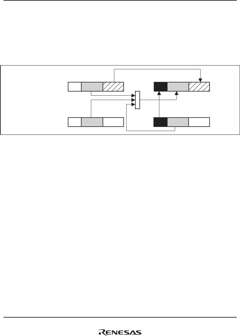
13. PCI Controller (PCIC)
Rev.1.00 Jan. 10, 2008 Page 635 of 1658
REJ09B0261-0100
For PCI memory space 2 accesses, the middle eleven bits ([28:18]) are controlled by PCIMBMR2.
• PCIMBMR2 [28:18] B'1 1111 1111 11: PCI address [28:18] = SuperHyway bus address [28:18]
• PCIMBMR2 [28:18] B'0 0000 0000 00: PCI address [28:18] = PCIMBR2 [28:18]
The upper three bits ([31:29]) of a SuperHyway bus address are replaced with bits 31 to 29 in
PCIMBR2.
SHwy bus address PCI address
PCIMBMR2 PCIMBR2
mask
31 29 28 18 17 0
31 29 28 18 17 0
31 29 28 18 17 0
31 29 28 18 17 0
Figure 13.5 Access from SuperHyway Bus to PCI Memory (PCI Bus)
(PCI Memory Space 2)
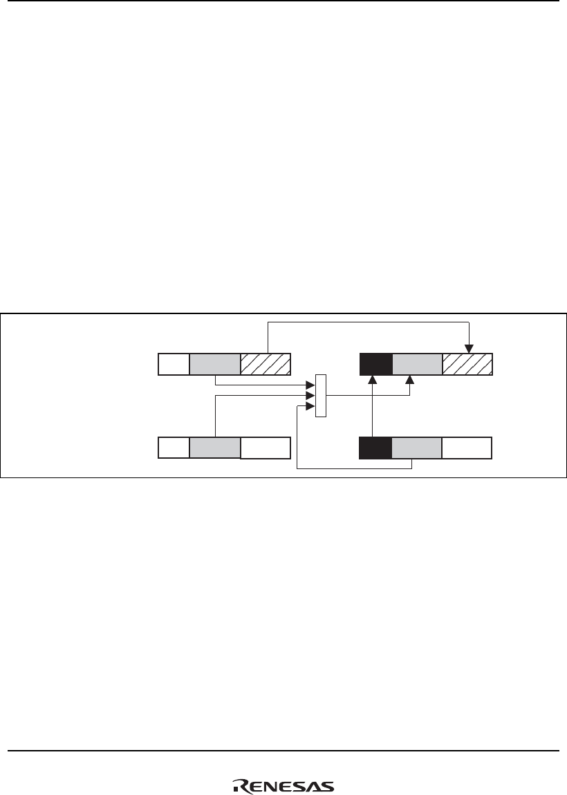
13. PCI Controller (PCIC)
Rev.1.00 Jan. 10, 2008 Page 636 of 1658
REJ09B0261-0100
(3) Accessing PCI I/O Space
Burst transfers are not supported in I/O transfers. Access within the size of 4-byte.
The PCI I/O address space is allocated from H'FD20 0000 to H'FE3F FFFF (2 Mbytes).
Address translation from SuperHyway bus to PCI local bus is shown below.
The lower 15 bits ([17:3]) of a SuperHyway bus address are sent without translation.
The middle bits ([20:18]) of a SuperHyway bus address are controlled by PCIIOBMR.
• PCIIOMR0 [20:18] B'111: PCI address [20:18] = SuperHyway bus address [20:18]
• PCIIOMR0 [20:18] B'000: PCI address [20:18] = PCIIOBR [20:18]
The upper eleven bits ([31:21]) of a SuperHyway bus address are replaced with bits 31 to 21 in
PCIIOBR.
SHwy bus address PCI address
PCIIOBMR PCIIOBR
mask
31 21 20 18 17 0
31 21 20 18 17 0
31 21 20 18 17 0
31 21 20 18 17 0
Figure 13.6 Access from SuperHyway Bus to PCI I/O Space (PCI Bus)
(4) Accessing Internal Registers of This LSI
All internal registers, that is, PCIECR, PCI configuration registers, and PCI local registers can be
accessed through the CPU. 4-byte, 2-byte, and 1-byte transmission are supported.
(5) Endian
The PCIC in this LSI supports both the big endian and little endian formats. Since the PCI bus
supports little endian, the PCIC supports both byte swapping and non-byte swapping.
The endian format setting is specified by the TBS bit in PCICR.
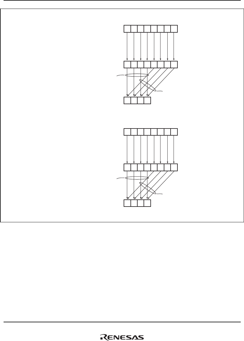
13. PCI Controller (PCIC)
Rev.1.00 Jan. 10, 2008 Page 637 of 1658
REJ09B0261-0100
MSB
31 0
LSB
SHwy data
PCI bus data
1. Little endian
A' B' C' D' A B
C
A' B' C' D' A B
A B C
PCI_Addr[2] = 1
PCI_Addr[2] = 0
31 0
SHwy data
PCI bus data
2. Big endian
A B C D A' B' C' D'
ABC
PCI_Addr[2] = 0
PCI_Addr[2] = 1
Note: PCIAddr[2]: PCI bus AD[2]
D
Buffer data
Buffer data
D
CD
MSB LSB
A B C D A' B' C' D'
D
Figure 13.7 Endian Conversion from SuperHyway Bus to PCI Bus
(Non-Byte Swapping: TBS = 0)
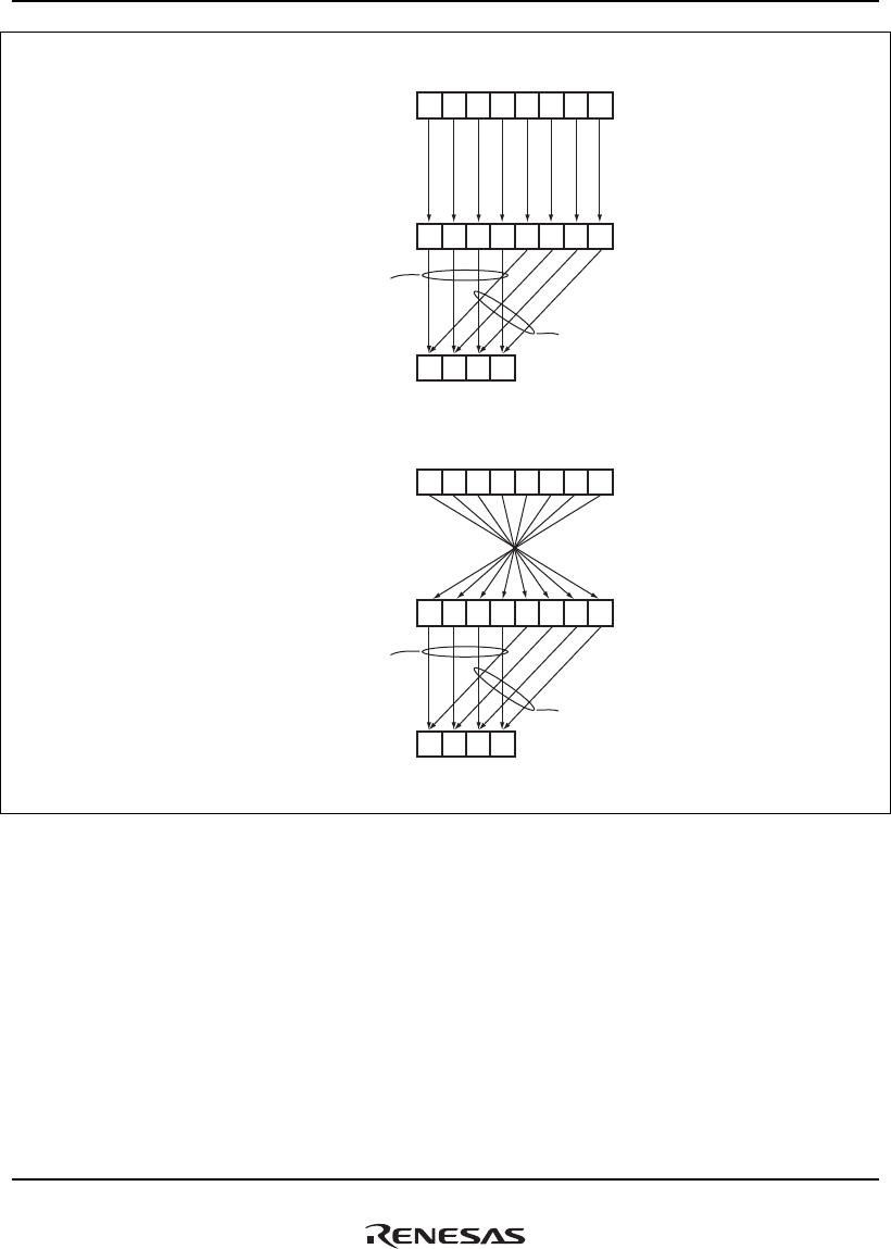
13. PCI Controller (PCIC)
Rev.1.00 Jan. 10, 2008 Page 638 of 1658
REJ09B0261-0100
MSB
31 0
LSB
SHwy data
PCI bus data
1. Little endian
A' B' C' D' A B C
A' B' C' D' A BC
D
D
ABCD
PCI_Addr[2] = 1
PCI_Addr[2] = 0
MSB
31 0
LSB
SHwy data
PCI bus data
2. Big endian
D C B A D' C' B' A'
A B C D A' B' C' D'
A B C
PCI_Addr[2] = 1
PCI_Addr[2] = 0
Note: PCIAddr[2]: PCI bus AD[2]
D
Buffer data
Buffer data
Figure 13.8 Endian Conversion from SuperHyway Bus to PCI Local Bus
(Byte Swapping: TBS = 1)
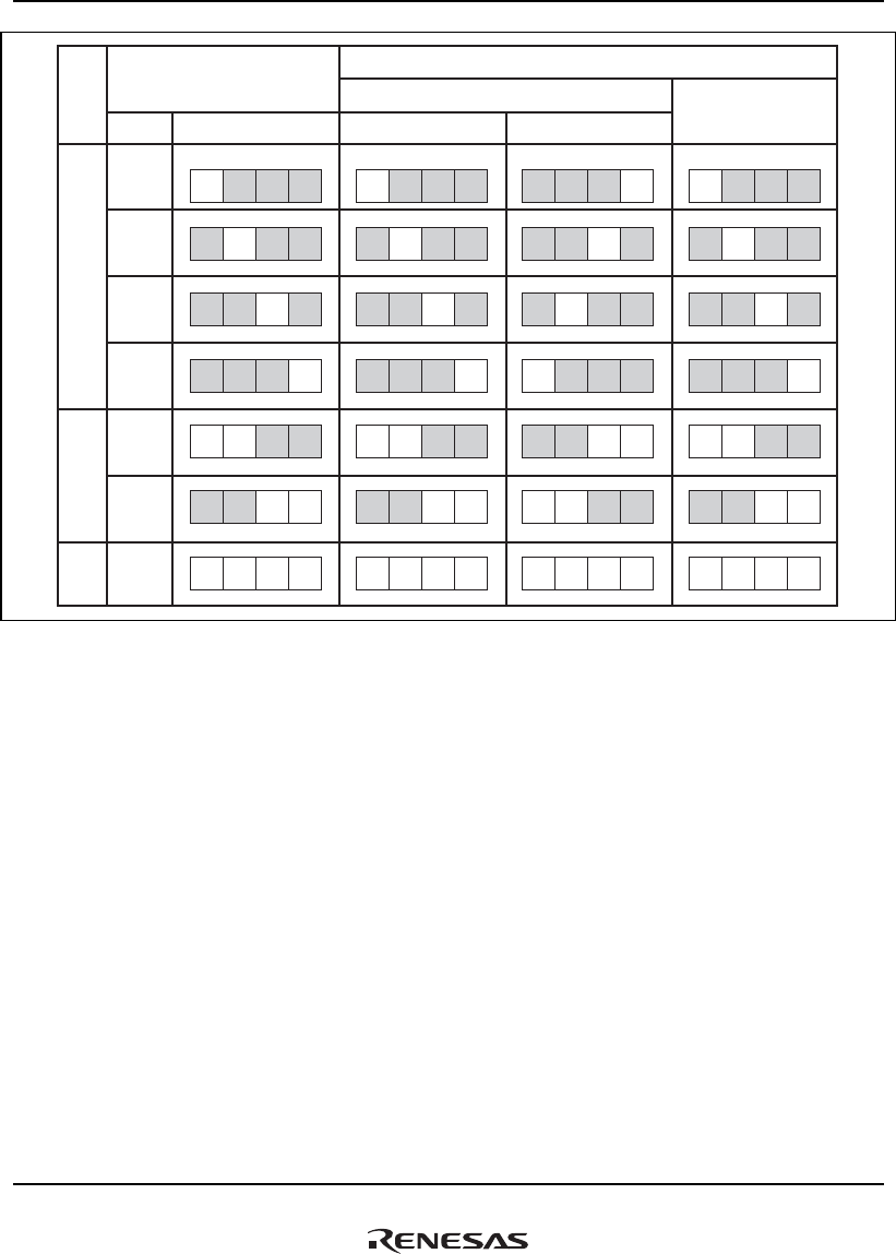
13. PCI Controller (PCIC)
Rev.1.00 Jan. 10, 2008 Page 639 of 1658
REJ09B0261-0100
31 0
A
31 0
A
31 0
A
31 0
A
B B B B
C C C C
D D D D
AB AB BA AB
CD CD DC CD
CDAB CD DC CDAB ABBA
Size
Byte
Word
long-
word
Address
4n + 0
4n + 1
4n + 2
4n + 3
4n + 0
4n + 2
4n + 0
SHwy bus
PCI bus
Big-endian CPU
Data Data (without swapping) Data (with swapping)
Little-endian CPU
Figure 13.9 Data Alignments for SuperHyway Bus and PCI Bus
13. PCI Controller (PCIC)
Rev.1.00 Jan. 10, 2008 Page 640 of 1658
REJ09B0261-0100
13.4.4 Target Access
This section describes how the PCIC in this LSI is accessed by an external PCI local bus master
when the PCIC is used in both the host mode and normal mode.
(1) Accessing Memory Space in This LSI
Accesses to the PCIC in this LSI by an external PCI bus master are described below.
I/O space
SHwy bus address space (4GB)PCI bus address space (4GB)
H'00000000
Local address
space 0 (base 0)
Memory base 1
I/O base
PCI I/O space
Memory base 0
H'FE000000
H'FE3FFFFF
H'FFFFFFFF
H
'00000000
H'FFFFFFFF
Local address
space 1 (base 1)
Figure 13.10 Memory Map from PCI Bus to SuperHyway Bus

13. PCI Controller (PCIC)
Rev.1.00 Jan. 10, 2008 Page 641 of 1658
REJ09B0261-0100
To access the address space in this LSI, use PCIMBAR0/1, PCILSR0/1, and PCILAR0/1. PCI
addresses can be allocated to by software. The PCIC has two types of registers for memory
mapping, Local Address Space 0 (base 0) and Local Address Space 1 (base 1).
By setting these two registers, two types of spaces (bases) can be allocated.
The size of these address spaces are selectable from 1 Mbyte to 512 Mbytes by PCILSR0/1.
Single-longword (32 bits) and burst transfers on the PCI bus are supported for PCI target memory
transfers.
For details of accesses to PCIC internal registers (PCI configuration registers and PCI local
registers), see after-mentioned description for configuration access and access to I/O space.
A certain range of the address space on the PCI bus corresponds to the local address space in the
internal bus address space. The local address space 0 in this LSI is controlled by PCIMBAR0,
PCILSR0 and PCILAR0. The local address space 1 is controlled by PCIMBAR1, PCILSR1 and
PCILAR1. Figure 13.11 shows the address translation from the PCI bus to the SuperHyway bus in
this LSI.
PCIMBAR indicates the start address of the PCI bus memory space used by an external PCI
device. PCILAR indicates the start address of the local address space for this LSI. PCILSR
indicates the size of the address space used by an external PCI device.
For PCIMBAR and PCILAR, the upper address bits that are higher than the memory size set in
PCILSR becomes valid. The upper bits in PCIMBAR and the PCI address output from an external
PCI device are compared to determine whether the PCIC is accessed. If these addresses match, an
access to the PCIC is recognized, and a local address is generated from the upper bits in PCILAR
and the lower bits of the PCI address output from the external PCI device. A PCI command
(memory read/write) is executed for this address. If the upper bits of the PCI address output from
the external PCI device does not match the upper bits of PCIMBAR, the PCIC does not respond to
a PCI command.
The PCIC supports data prefetching for a memory read command. When burst read is performed
on the PCI bus, data is prefetched in block units of 8 bytes or 32 bytes (set by PCICR.PFCS and
PCICR.PFE).
When all the MBARE bits in PCILSR0/1 are 0, a PCI bus address is transferred to the internal bus
without translation.
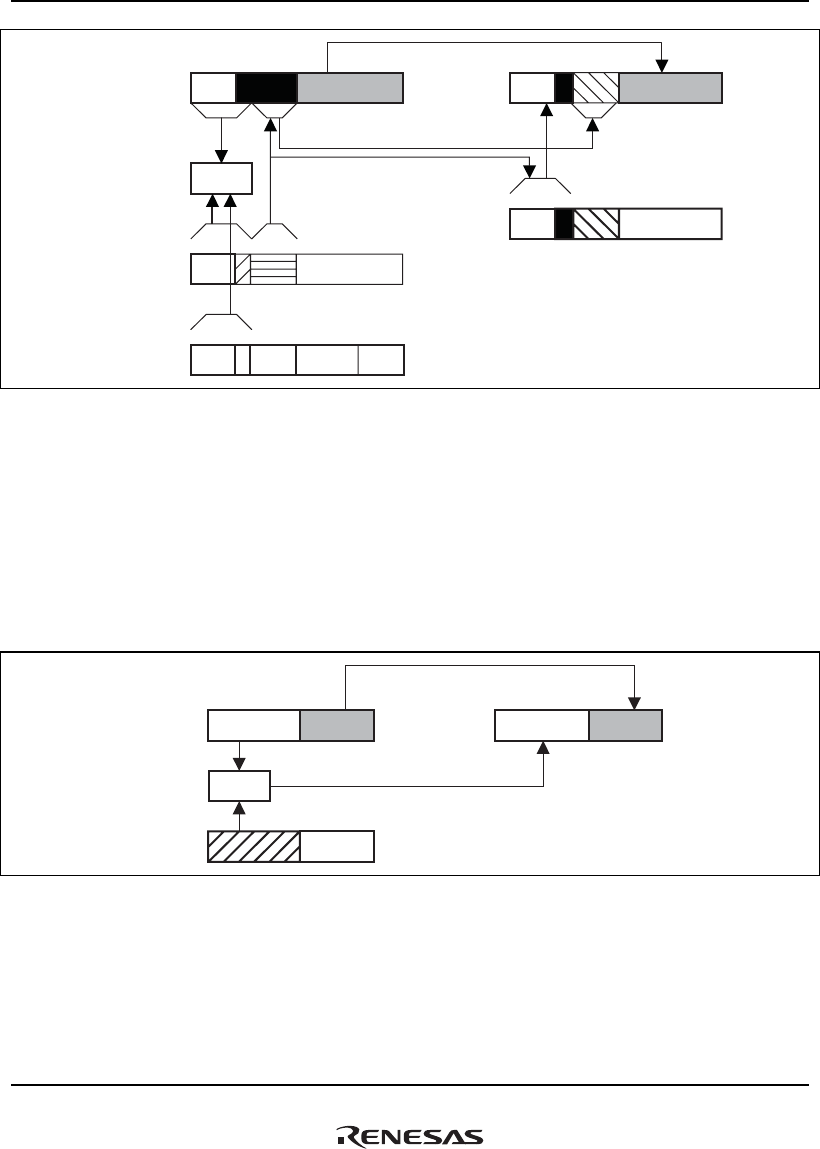
13. PCI Controller (PCIC)
Rev.1.00 Jan. 10, 2008 Page 642 of 1658
REJ09B0261-0100
MBARE
PCI address
31 28 20 0 29 19
PCIMBAR0/1
PCILSR0/1
PCILAR0/1
SHwy bus
address
Compare
0
31 20 0
29
0
31 28 20 0 29 19
1928
31 2029 1928
31 2029 1928
Figure 13.11 PCI Bus to SuperHyway Bus Address Translation
(2) Accessing PCIC I/O Space
The PCI I/O address space should be allocated as 256 bytes.
The lower eight bits ([7:0]) are sent to the internal bus without translation.
When bits 31 to 8 of a PCI address match bits 31 to 8 of PCIIBAR, the upper 24 bits are replaced
with H'FE04 01 and a PCI local register is accessed.
PCI address
PCI address
SHwy bus address
31 8 7 0
31 8 7 0
31 8 7 0
Compare
H'FE0401
Figure 13.12 I/O Access from PCI Bus to SuperHyway Bus

13. PCI Controller (PCIC)
Rev.1.00 Jan. 10, 2008 Page 643 of 1658
REJ09B0261-0100
(3) Accessing PCIC Registers
Configuration Registers: Configuration registers should be read or written with (offset from
configuration register space base address) by configuration accesses. A burst transfer is cut off and
terminated.
Local Registers: Local registers should be accessed with (PCI address + offset) using I/O read or
write commands. Only a single longword access is supported. A burst transfer is cut off and
terminated.
Control Register (PCIECR): The control register space should not be read or written from the
PCI bus using a memory read/write command.
(4) Access to SH7785
Memory Space: See Section 13.4.4 (1), Accessing Memory Space in This LSI. Areas 0 to 6 (CS0
to CS6) on the SH7785 memory map, DDR2-SDRAM space and URAM/ILRAM/OLRAM in the
SH-4A core can be accessed.
On-chip IO Space: The on-chip I/O space should not be read or written from the PCI bus using a
memory read/write command. The read/write operation is not guaranteed.
(5) Exclusive Access
The lock accessing on the PCI bus is supported.
When the PCI bus is locked, the PCIC is accessible from the device that asserts LOCK.
Resource lock on the SuperHyway bus is not supported. (Another on-chip module can access the
PCIC during lock transfer.)
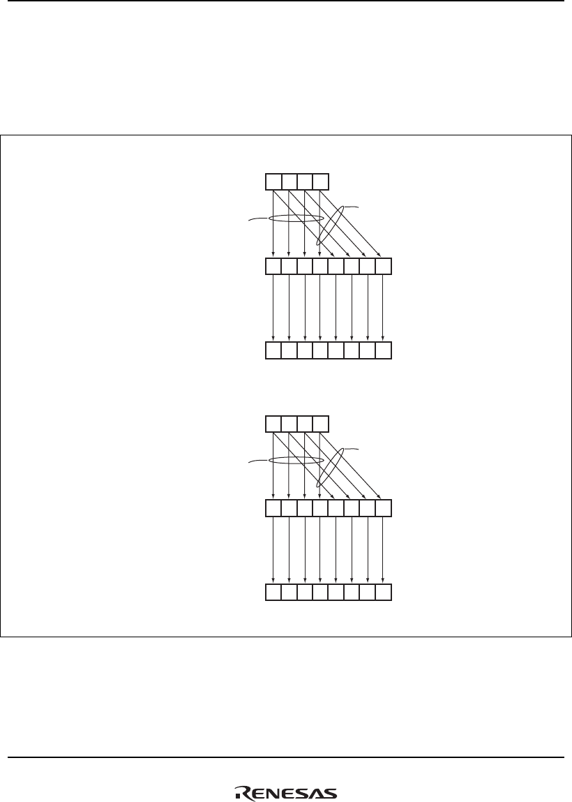
13. PCI Controller (PCIC)
Rev.1.00 Jan. 10, 2008 Page 644 of 1658
REJ09B0261-0100
(6) Endian
This LSI supports both the big and little endian formats. Since the PCI local bus is inherently little
endian, the PCIC supports both byte swapping and non-byte swapping.
The endian format is specified by the TBS bit in PCICR.
31
MSB LSB
0
PCI bus data
SHwy data
1. Little endian
A' B' C' D' ABC
A' B' C' D' ABCD
A B C
PCI_Addr[2] = 1
PCI_Addr[2] = 0
31
MSB LSB
0
PCI bus data
SHwy
data
AB C D A' B' C' D'
A B C D A' B' C' D'
A B C
PCI_Addr[2] = 0
PCI_Addr[2] = 1
2. Big endian
Note: PCIAddr[2]: PCI bus AD[2]
D
D
Buffer data
Buffer data
D
Figure 13.13 Endian Conversion from PCI Bus to SuperHyway Bus
(Non-Byte Swapping: TBS = 0)
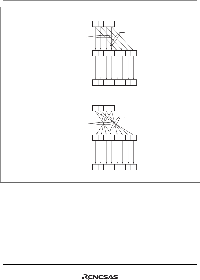
13. PCI Controller (PCIC)
Rev.1.00 Jan. 10, 2008 Page 645 of 1658
REJ09B0261-0100
31
MSB LSB
0
PCI bus data
SHwy data
1. Little endian
A' B' C' D' A B C
A' B' C' D' A B C
ABCD
PCI_Addr[2] = 1
PCI_Addr[2] = 0
31
MSB LSB
0
PCI bus data
SHwy
data
DC B A D' C' B' A'
D C B A D' C' B' A'
A B C
PCI_Addr[2] = 0
PCI_Addr[2] = 1
2. Big endian
Note: PCIAddr[2]: PCI bus AD[2]
D
D
D
Buffer data
Buffer data
Figure 13.14 Endian Conversion from PCI Bus to SuperHyway Bus
(Byte Swapping: TBS = 1)
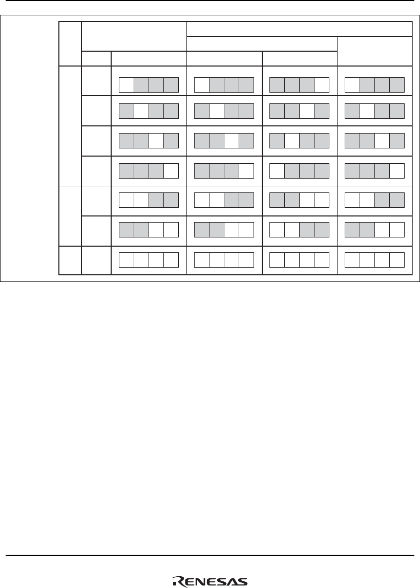
13. PCI Controller (PCIC)
Rev.1.00 Jan. 10, 2008 Page 646 of 1658
REJ09B0261-0100
31 0
A
31 0
A
31 0
A
31 0
A
B B B B
C C C C
D D D D
AB AB BA AB
CD CD DC CD
CDAB CD DC CDAB ABBA
Size
Byte
Word
Long-
word
Address
4n + 0
4n + 1
4n + 2
4n + 3
4n + 0
4n + 2
4n + 0
PCI bus
SHwy bus
Big-endian CPU
Data Data (without swapping) Data (with swapping)
Little-endian CPU
Figure 13.15 Data Alignments for SuperHyway Bus and PCI Bus
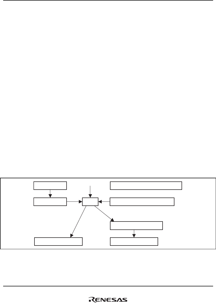
13. PCI Controller (PCIC)
Rev.1.00 Jan. 10, 2008 Page 647 of 1658
REJ09B0261-0100
(7) Cache Coherency
The PCIC supports cache coherency function.
When the PCIC functions as a target device, cache coherency is guaranteed on the PCI bus for
accesses from a master device both in host mode and normal mode. When a cacheable area of this
LSI is accessed, PCICSCR0/1 and PCICSAR0/1 should be set.
The following shows the usage notes for this function.
• Up to two conditions can be set for the snoop address. These two conditions are logical ORed
for address comparison.
• When this function is used, a flush/purge request is issued to the CPU before memory
read/write is performed in an access by an address hit. It seriously reduces the PCI bus transfer
speed and CPU performance.
• Do not use the prefetch function when using this function. (Do not set the PFE bit in PCICR to
1.)
• Do not use this function when the CPU is in the sleep state. If a cache hit occurs when the CPU
is in the sleep state, an error occurs on the SuperHyway bus and memory read/write is not
performed. Specify the SNPMD bit (snoop mode) in PCICSCR to 00 (to turn off the snoop
function) before the CPU enters the sleep mode. To keep the coherency before/after the CPU
enters the sleep state, execute cache purge before the sleep instruction is executed.
• When using this function, do not use debugging functions using an emulator. (Do not use this
function when using an emulator).
PCI bus address
Internal bus address Cache snoop address register
Compare
Execute read/write
Cache flash/purge
Execute read/write
No hit
Hit
Cache snoop control register
Set
Figure 13.16 Cache Flush/Purge Execution Flow from PCI Bus to SuperHyway Bus

13. PCI Controller (PCIC)
Rev.1.00 Jan. 10, 2008 Page 648 of 1658
REJ09B0261-0100
13.4.5 Host Mode
(1) Operation in Host Mode
The PCI interface of this LSI supports a subset of the PCI version 2.2 and can be connected to a
device with a PCI bus interface.
According to the PCIC mode, host mode or normal mode, operation differs in two points: (1) the
PCIC unconditionally performs bus parking or not, and (2) the PCI bus arbitration function is
enabled or disabled.
In host mode, the PCIC drives the AD, C/BE, PAR signal lines when a transfer is not performed
on the PCI bus. When the PCIC subsequently starts a transfer as the master, the PCIC continues to
drive these signal lines until the address phase ends.
The REQ and GNT signals between PCIC and an arbiter in the PCIC are internally connected.
Here, pins REQ0/REQOUT, REQ1, REQ2, and REQ3 function as the REQ inputs from external
masters 0 to 3. Similarly, GNT0/GNTIN, GNT1, GNT2, and GNT3 function as the GNT outputs
to external masters 0 to 3. Arbitration for five masters including the PCIC can be performed.
(2) Configuration Space Access
The PCIC supports configuration mechanism #1. The PCI PIO address register (PCIPAR) and PCI
PIO data register (PCIPDR) correspond to the configuration address register and configuration
data register, respectively.
When PCIPAR is set and PCIPDR is read or written to, a configuration cycle is issued on the PCI
bus. For the type-0 transfer, bits 10 to 2 of the configuration address register are sent to the PCI
bus without translation and AD31 to AD11 are changed to be used as the IDSEL signal.
When the device number is set to 0, AD16 is driven to 1 and the other bits are made to be 0.
When the device number is set to 1, AD17 is driven to 1 and the other bits are made to be 0.
Similarly, setting the device number to 2 drives AD18 to 1 and setting the device number to 3
drives AD19 to 0.
When the device number is set to 16, AD31 is driven to 1 and the other bits are made to be 0.

13. PCI Controller (PCIC)
Rev.1.00 Jan. 10, 2008 Page 649 of 1658
REJ09B0261-0100
31 30 24 16
23 15 1110 87 2 1 0
Configuration address
register
PCI bus address
Reserved Bus No.
Function
No.
Register No.
0 0
0 0 Only one bit is set to 1.
31 1110 8 7 2 1 0
Enable bit
0: Disabled
1: Enabled
Device No.
Figure 13.17 Address Generation for Type 0 Configuration Access
In configuration accesses, no interrupt is generated by a PCI master abort (no device connected).
A configuration write will end normally. A configuration read will return a value of 0.
(3) Arbitration
In host mode, the PCI bus arbiter in the PCIC is activated.
The PCIC supports four external masters (four pairs of REQ and GNT).
If the bus usage is simultaneously requested by two devices or more, the bus arbiter accepts the
request of the highest priority device.
The PCI bus arbiter supports two modes to determine the device priority: (1) fixed priority and (2)
pseudo-round-robin. The mode is selected by the BMAM bit in PCICR.
In the following description, the device n indicates a PCI device that uses REQn.
(a) Fixed Priority: When the BMAM bit in PCICR is cleared to 0, the priorities of devices are
fixed by the default as follows:
PCIC > device 0 > device 1 > device 2 > device 3
The PCIC has the priority to use the bus in comparison with other devices.
(b) Pseudo-Round-Robin: When the BMAM bit in PCICR is set to 1, the most recently permitted
device is assigned as the lowest priority.
The initial priority is the same as that of the fixed priority mode.
After the device 1 requires the bus and transfer data and the request is permitted, the priority
changes as follows:
PCIC > device 0 > device 2 > device 3 > device 1

13. PCI Controller (PCIC)
Rev.1.00 Jan. 10, 2008 Page 650 of 1658
REJ09B0261-0100
Subsequently, after the PCIC requires the bus and transfer data and the request is permitted, the
priority changes as follows:
Device 0 > device 2 > device 3 > device 1 > PCIC
Then, after the device 3 requires the bus and transfer data and the request is permitted, the priority
changes as follows:
Device 0 > device 2 > device 1 > PCIC > device 3
(4) Interrupts
• The PCIC has 10 interrupts (these signals are connected to the INTC of this LSI)
• Interrupts are enabled/disabled and their priority levels are specified by the INTC of this LSI
• When the PCIC operates in normal mode, INTA output is available as an interrupt to the host
device on the PCI bus. The INTA pin can be set to be asserted or negated by the IOCS bit in
PCICR.
Table 13.6 Interrupt Priority
Signal Interrupt Source INTEVT Priority
PCISERR SERR assertion detected in host mode H'A00 High
PCIINTA PCI interrupt A (INTA) assertion detected in host mode H'A20
PCIINTB PCI interrupt B (INTB) assertion detected in host mode H'A40
PCIINTC PCI interrupt C (INTC) assertion detected in host mode H'A60
PCIINTD PCI interrupt D (INTD) assertion detected in host mode H'A80
PCIEER A PCI error occurs. Generated by PCIIR and PCIAINT.
(Maskable)
H'AA0
PCIPWD3 Power state transition to D3. Generated by PCIPINT.
(Maskable)
PCIPWD2 Power state transition to D2. Generated by PCIPINT.
(Maskable)
PCIPWD1 Power state transition to D1. Generated by PCIPINT.
(Maskable)
H'AC0
PCIPWD0 Power state transition to D0. Generated by PCIPINT.
(Maskable)
H'AE0
Low

13. PCI Controller (PCIC)
Rev.1.00 Jan. 10, 2008 Page 651 of 1658
REJ09B0261-0100
The PCIC can retain error information on the PCI bus. When an error occurs, the error address is
stored in PCIAIR and the transfer type and command information are stored in PCICIR. When the
PCIC is in host mode, the bus master information at the error occurrence is stored in PCIBMIR.
The PCIC can retain only one error information. Therefore, when multiple errors occur, only the
first error information is retained and subsequent error information is not retained. The error
information is initialized by a power-on reset.
13.4.6 Normal Mode
In normal mode, the bus arbiter in the PCIC does not operate. The PCI bus arbitration is
performed by an external PCI bus arbiter.
The Bus master that performs bus parking is decided by the GNT signal output from the external
bus arbiter. If the master that performs bus parking and the master that starts the next transfer are
different, high-impedance state is generated for one clock cycle or more before the address phase.
The GNT0/GNTIN pin is used for the GNT input to the PCIC, and the REQ0/REQOUT pin is
used for the REQ output from the PCIC.
13.4.7 Power Management
The PCIC has PCI power management configuration registers (supporting subsets in version 1.1).
The following shows the supported features:
• Supports the PCI power management control configuration registers
• Supports the power-down/restore request interrupts from a host device on the PCI bus
The PCIC supports seven configuration registers for PCI power management control. PCICP
indicates the address offset for the power management configuration registers. In the PCIC,
PCICP is fixed to H'40. PCICID, PCINIP, PCIPMC, PCIPMCSR, PCIPMCSRBSE and PCIPCDD
are power management registers. These registers support four states: power state D0 (normal state)
power state D1 (bus idle state) power state D2 (clock stopped state) and power state D3 (power
down mode).
Figure 13.18 shows power down state transitions on the PCI bus.
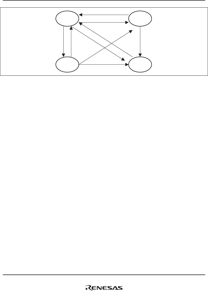
13. PCI Controller (PCIC)
Rev.1.00 Jan. 10, 2008 Page 652 of 1658
REJ09B0261-0100
D0
(Nomal state)
D2
(Clock stopped)
D1
(Bus idle)
D3
(Power-down)
Figure 13.18 Power Down State Transitions on PCI Bus
When the PCIC detects that the power state (PS) bit in PCIPMCSR changes (PS is written by an
external PCI device), it issues a power management interrupt. PCIPINT and PCIPINTM are used
to control the power management interrupts. As the power management interrupts, PCIPWD0 that
detects a transition from the power state D1/D2/D3 to D0, PCIPWD1 that detects a transition from
the power state D0 to D1, PCIPWD2 that detects a transition from the power state D0/D1 to D2,
and PCIPWD3 that detects a transition from the power state D0/D1/D2 to D3 are supported. An
interrupt mask can be set for each interrupt.
The power state D0 interrupt is not generated at a power-on reset.
When the PCIC operates in normal mode and accepts a power down interrupt from an external
host device, note the following:
With the PCI power management function, the PCI bus clock is stopped 16 clocks or more after
the host device directs a transition to the power state D3. Therefore, after detecting a power state
D3 interrupt, do not attempt to read or write to the PCIC internal local registers and configuration
registers that can be accessed both from the CPU and PCI bus, and PCI local bus accesses (I/O and
memory spaces). If the PCI bus clock stops during the access, the read/write cycle will not be
completed and hung up on the SuperHyway bus because these accesses operate with the PCI bus
clock

13. PCI Controller (PCIC)
Rev.1.00 Jan. 10, 2008 Page 653 of 1658
REJ09B0261-0100
13.4.8 PCI Local Bus Basic Interface
The PCI interface of this LSI supports subsets in the PCI bus version 2.2 and it can be connected
to a device with a PCI bus interface. The following figures show the timing in each operating
mode.
(1) Master Read/Write Cycle Timing
Figure 13.19 shows an example of a single-write cycle in host mode. Figure 13.20 shows an
example of a single-read cycle in host mode. Figure 13.21 shows an example of a burst-write
cycle in normal mode. Figure 13.22 is an example of a burst-read cycle in normal mode. Note that
the response speed of DEVSEL and TRDY differs according to the connected target device. In
PIO transfer, a single read/write cycle should be used. The configuration transfers can be issued
only in host mode.
PCICLK
AD[31:0]
PAR
C/BE[3:0]
PCIFRAME
IRDY
DEVSEL
TRDY
IDSEL
REQ
GNT
Addr D0
AP DP0
Com BE0
Legend:
Addr: PCI space address
Dn: nth data
AP: Address parity
DPn: nth data parity
Com: Command
LOCK
BEn: nth data byte enable
Figure 13.19 Master Write Cycle in Host Mode (Single)
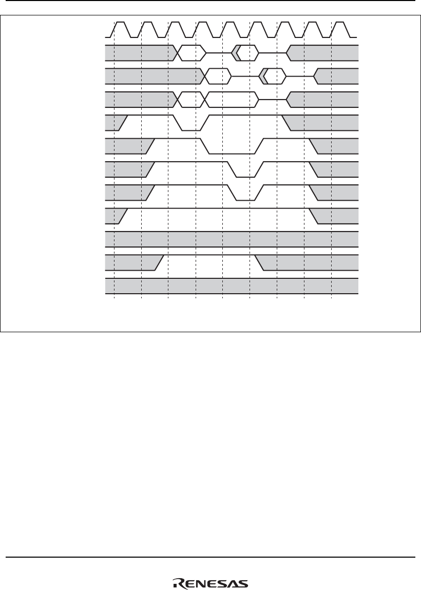
13. PCI Controller (PCIC)
Rev.1.00 Jan. 10, 2008 Page 654 of 1658
REJ09B0261-0100
PCICLK
AD[31:0]
PAR
C/BE[3:0]
PCIFRAME
IRDY
DEVSEL
TRDY
IDSEL
REQ
GNT
Addr D0
AP DP0
Com BE0
LOCK
Legend:
Addr: PCI space address
Dn: nth data
AP: Address parity
DPn: nth data parity
Com: Command
BEn: nth data byte enable
Figure 13.20 Master Read Cycle in Host Mode (Single)
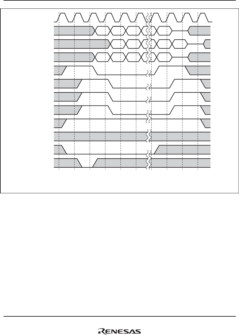
13. PCI Controller (PCIC)
Rev.1.00 Jan. 10, 2008 Page 655 of 1658
REJ09B0261-0100
Addr D0
AP DP0
Com BE0
D1
DPn-1 DPn
BE1 BEn
Dn
PCICLK
AD[31:0]
PAR
C/BE[3:0]
PCIFRAME
IRDY
DEVSEL
TRDY
IDSEL
REQOUT
GNTIN
Legend:
Addr: PCI space address
Dn: nth data
AP: Address parity
DPn: nth data parity
Com: Command
LOCK
BEn: nth data byte enable
Figure 13.21 Master Write Cycle in Normal Mode (Burst)
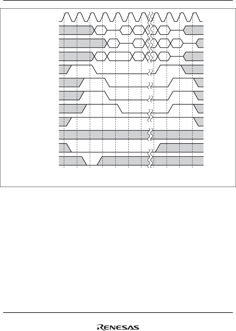
13. PCI Controller (PCIC)
Rev.1.00 Jan. 10, 2008 Page 656 of 1658
REJ09B0261-0100
Addr D0
AP DP0
Com BE0
D1
DPn-1 DPn
BE1 BEn
Dn
PCICLK
AD[31:0]
PAR
C/BE[3:0]
PCIFRAME
IRDY
DEVSEL
TRDY
IDSEL
REQOUT
GNTIN
Legend:
Addr: PCI space address
Dn: nth data
AP: Address parity
DPn: nth data parity
Com: Command
LOCK
BEn: nth data byte enable
Figure 13.22 Master Read Cycle in Normal Mode (Burst)

13. PCI Controller (PCIC)
Rev.1.00 Jan. 10, 2008 Page 657 of 1658
REJ09B0261-0100
(2) Target Read/Write Cycle Timing
The PCIC returns retries to target memory read accesses from an external master until 8 longword
(32-bit) data are prepared in the PCIC internal FIFO. That is, the first target read is always
responded by a retry.
When a target memory write access is performed for the PCIC, the PCIC returns retries to all
subsequent target memory accesses until the write data is completely written to local memory.
Thus, the data contents are guaranteed when data written to the target is target-read immediately
after it was written.
Only single transfers are supported for target accesses to the configuration space and I/O space. If
a burst access request is issued, the external master is disconnected when the first transfer is
complete. Note that the DEVSEL response speed is fixed to 2 clocks (medium) for the target
access to the PCIC.
Figure 13.23 shows an example of a target single-read cycle in normal mode. Figure 13.24 shows
an example of a target single-write cycle in normal mode. Figure 13.25 shows an example of a
target burst-read cycle in host mode. Figure 13.26 shows an example of a target burst-write cycle
in host mode.
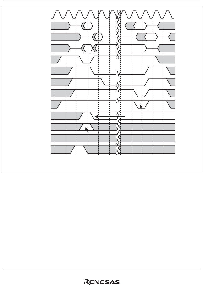
13. PCI Controller (PCIC)
Rev.1.00 Jan. 10, 2008 Page 658 of 1658
REJ09B0261-0100
Addr D0
AP DP0
Com BE0
Disconnect
Configuration space access
Lock
PCICLK
AD[31:0]
PAR
C/BE[3:0]
PCIFRAME
IRDY
DEVSEL
TRDY
IDSEL
REQOUT
GNTIN
Legend:
Addr: PCI space address
Dn: nth data
AP: Address parity
DPn: nth data parity
Com: Command
LOCK
BEn: nth data byte enable
STOP
Figure 13.23 Target Read Cycle in Normal Mode (Single)
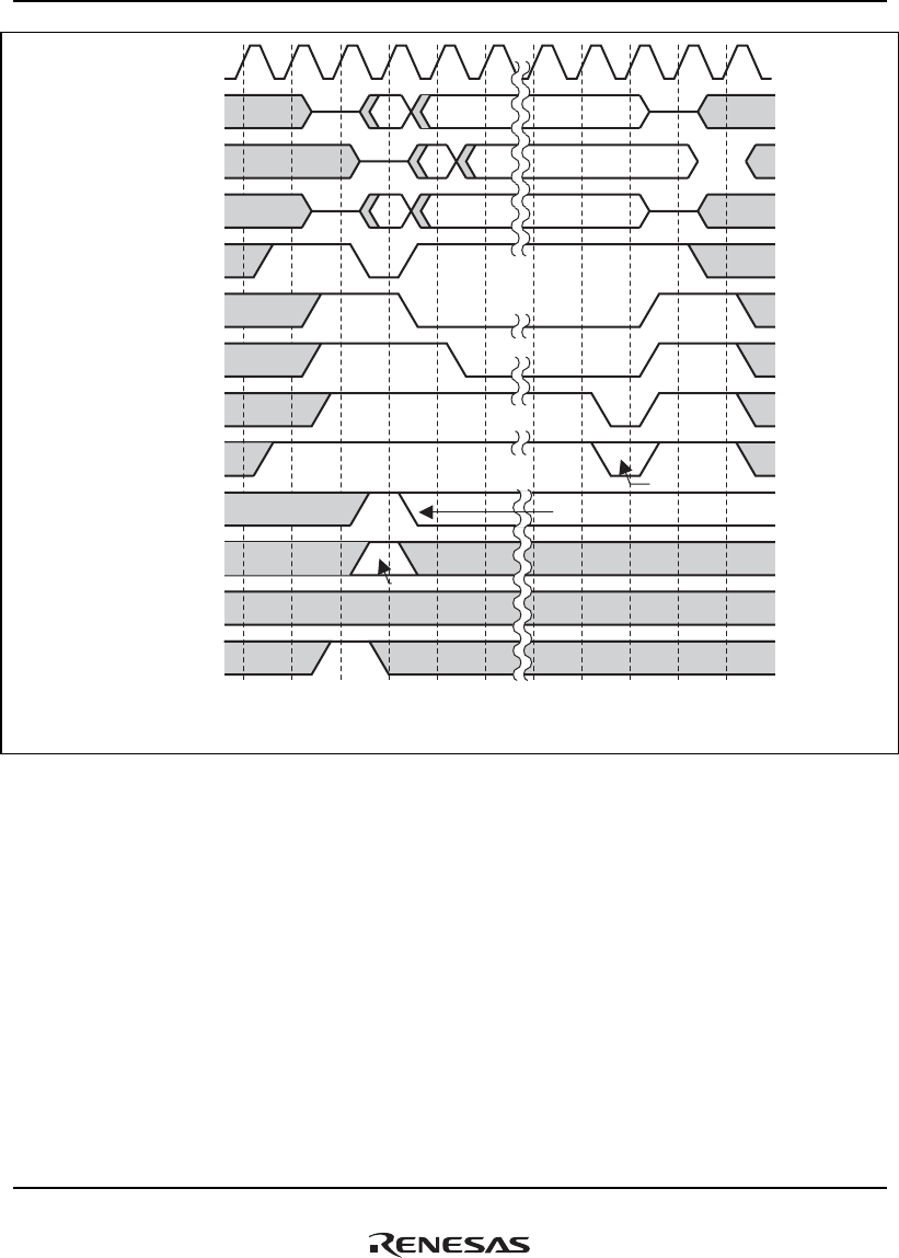
13. PCI Controller (PCIC)
Rev.1.00 Jan. 10, 2008 Page 659 of 1658
REJ09B0261-0100
DP0
Addr D0
AP
Com BE0
Disconnect
Configuration space access
Lock
PCICLK
AD[31:0]
PAR
C/BE[3:0]
PCIFRAME
IRDY
DEVSEL
TRDY
IDSEL
REQOUT
GNTIN
Legend:
Addr: PCI space address
Dn: nth data
AP: Address parity
DPn: nth data parity
Com: Command
LOCK
BEn: nth data byte enable
STOP
Figure 13.24 Target Write Cycle in Normal Mode (Single)

13. PCI Controller (PCIC)
Rev.1.00 Jan. 10, 2008 Page 660 of 1658
REJ09B0261-0100
Addr D0
AP DP0
Com BE0
Disconnect
Lock
D1
DPn-1 DPn
BE1 BEn
Dn
PCICLK
AD[31:0]
PAR
C/BE[3:0]
PCIFRAME
IRDY
DEVSEL
TRDY
IDSEL
REQ
GNT
Legend:
Addr: PCI space address
Dn: nth data
AP: Address parity
DPn: nth data parity
Com: Command
LOCK
BEn: nth data byte enable
STOP
Figure 13.25 Target Memory Read Cycle in Host Mode (Burst)
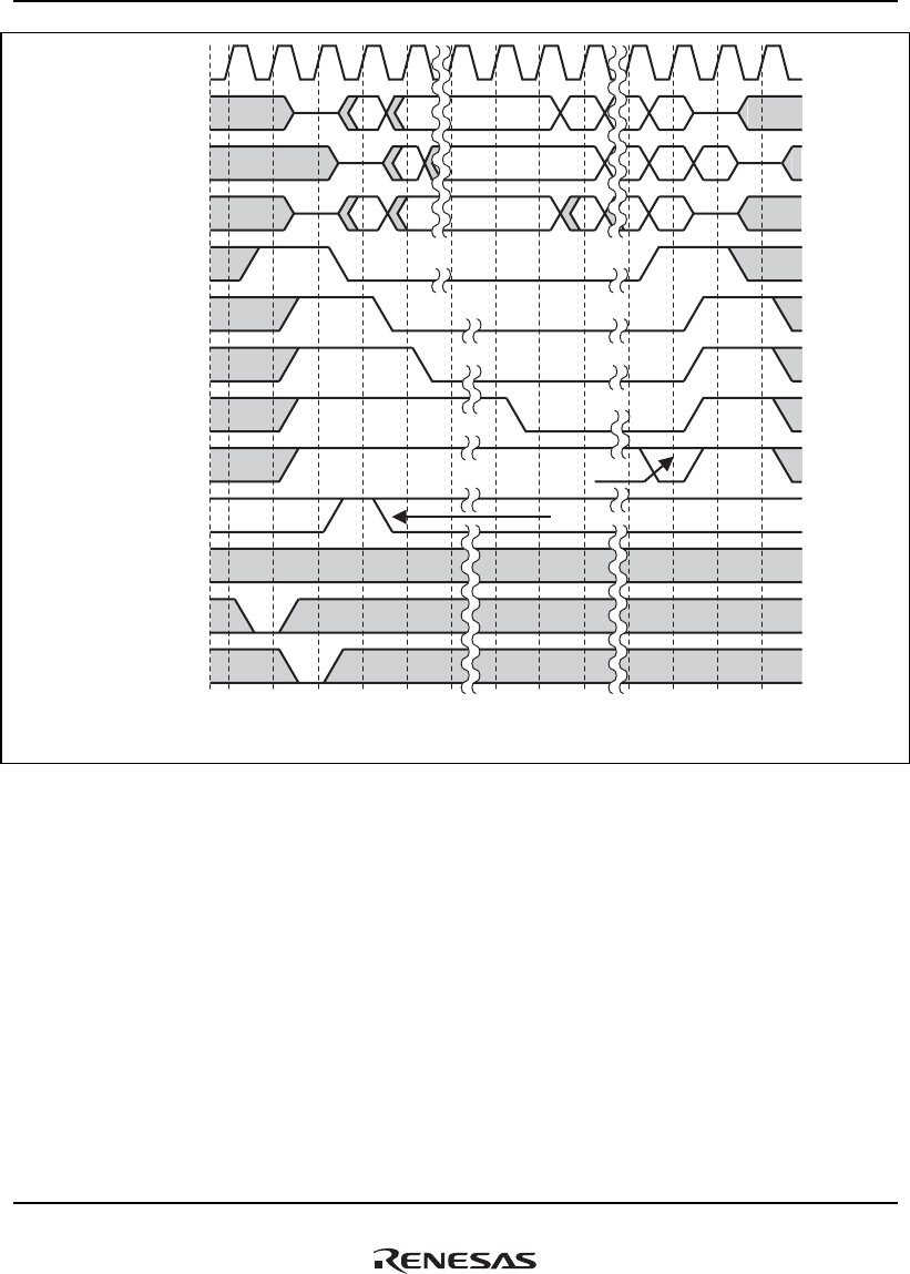
13. PCI Controller (PCIC)
Rev.1.00 Jan. 10, 2008 Page 661 of 1658
REJ09B0261-0100
Addr D0
AP DP0
Com BE0
Disconnect
Lock
D1
DPn-1 DPn
BE1 BEn
Dn
PCICLK
AD[31:0]
PAR
C/BE[3:0]
PCIFRAME
IRDY
DEVSEL
TRDY
IDSEL
REQ
GNT
Legend:
Addr: PCI space address
Dn: nth data
AP: Address parity
DPn: nth data parity
Com: Command
LOCK
BEn: nth data byte enable
STOP
Figure 13.26 Target Memory Write Cycle in Host Mode (Burst)
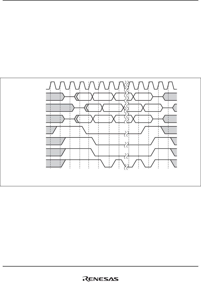
13. PCI Controller (PCIC)
Rev.1.00 Jan. 10, 2008 Page 662 of 1658
REJ09B0261-0100
(3) Address/Data Stepping Timing
By writing 1 to the SC bit in PCICMD, a wait (stepping) of one clock can be inserted when the
PCIC is driving the AD bus. As a result, the PCIC drives the AD bus with 2 clocks. This function
can be used when the PCI bus load is heavy and the AD bus does not achieve the stipulated logic
level in one clock.
It is recommended to use this function when the PCIC issues configuration transfers in host mode.
Figure 13.27 shows an example of a burst memory write cycle with address stepping. Figure 13.28
shows an example of a target burst read cycle with address stepping.
Addr D0
AP DP0
Com BE0
Dn
DPn-1 DPn
BEn
PCICLK
AD[31:0]
PAR
C/BE[3:0]
PCIFRAME
IRDY
DEVSEL
TRDY
Legend:
Addr: PCI space address
Dn: nth data
AP: Address parity
DPn: nth data parity
Com: Command
BEn: nth data byte enable
Figure 13.27 Master Write Cycle in Host Mode (Burst, with Stepping)
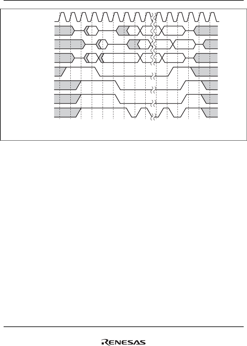
13. PCI Controller (PCIC)
Rev.1.00 Jan. 10, 2008 Page 663 of 1658
REJ09B0261-0100
D1
BE1
PCICLK
AD[31:0]
PAR
C/BE[3:0]
PCIFRAME
IRDY
DEVSEL
TRDY
Legend:
Addr: PCI space address
Dn: nth data
AP: Address parity
DPn: nth data parity
Com: Command
BEn: nth data byte enable
Addr D0
AP DP0
Com BE0
Dn
DPn-1 DPn
BEn
Figure 13.28 Target Memory Read Cycle in Host Bus Bridge Mode (Burst, with Stepping)

13. PCI Controller (PCIC)
Rev.1.00 Jan. 10, 2008 Page 664 of 1658
REJ09B0261-0100

14. Direct Memory Access Controller (DMAC)
Rev.1.00 Jan. 10, 2008 Page 665 of 1658
REJ09B0261-0100
Section 14 Direct Memory Access Controller (DMAC)
This LSI includes an on-chip direct memory access controller (DMAC). Instead of the CPU, the
DMAC can be used to perform data transfers among external devices equipped with DACK
(transfer request acceptance signal), external memory, on-chip memory, memory-mapped external
devices, and on-chip peripheral modules.
14.1 Features
• Number of channels: Twelve channels (channels 0 to 3 can accept an external request)
• Address space: 4 Gbytes on the architecture (Physical address)
• Transfer data length: Byte, word (2 bytes), longword (4 bytes), 16 bytes, and 32 bytes
• Maximum transfer count: 16,777,216
• Address mode: Dual address mode
• Transfer requests:
Choice of external request (channels 0 to 3), on-chip peripheral module request, or auto-
request
The following modules can issue an on-chip peripheral module request.
⎯ SCIF0 to SCIF5, HAC0, HAC1, HSPI, SIOF, SSI0, SSI1, FLCTL, and MMCIF
• Bus mode:
Choice of cycle steal mode (normal mode or intermittent mode) or burst mode
• Priority: Choice of fixed mode and round-robin mode
• Interrupt request: An interrupt request can be generated to the CPU after half of transfers have
ended, all transfers have ended, or an address error has occurred
• External request detection: Choice of low/high level detection and rising/falling edge detection
of DREQ input
• DMA transfer end notification signal: Active levels for DACK can be specified independently
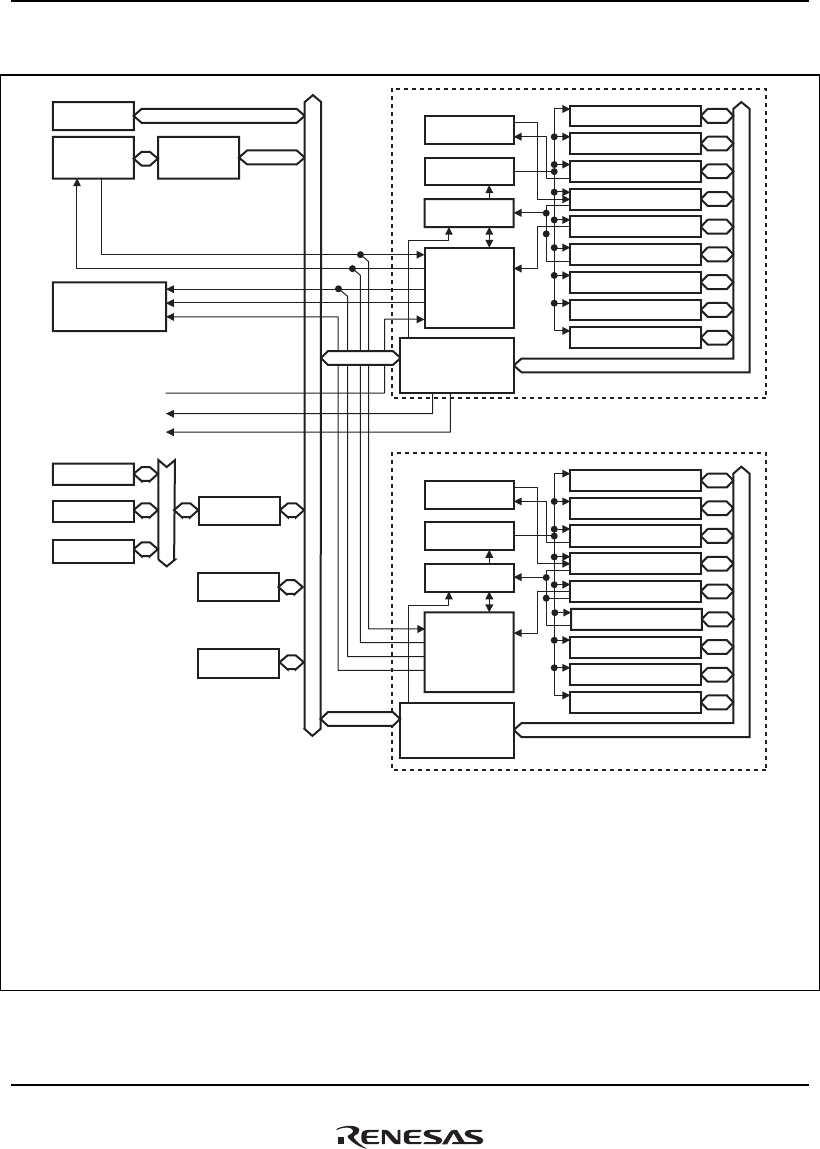
14. Direct Memory Access Controller (DMAC)
Rev.1.00 Jan. 10, 2008 Page 666 of 1658
REJ09B0261-0100
Figure 14.1 shows a block diagram of the DMAC.
Peripheral
bus controller
DMA transfer end signal
Iteration
control
DMAC channels 6 to 11
Register
control
Start-up
control
Request
priority
control
Bus
interface
Iteration
control
DMAC channels 0 to 5
Register
control
Start-up
control
Request
priority
control
Bus
interface
On-chip
memory
On-chip
peripheral
module
Interrupt controller
DMA transfer request signal
External ROM
External RAM
External I/O
TCR0 to TCR5
CHCR0 to CHCR5
DMAOR0
DMARS0 to DMARS2
SAR0 to SAR5
DAR0 to DAR5
TCRB0 to TCRB3
SARB0 to SARB3
DARB0 to DARB3
DMINT0 to DMINT11
DMAE0
DMAE1
DRAK0 to DRAK3
DREQ0 to DREQ3
DACK0 to DACK3
LBSC
DDRIF
PCIC
TCR6 to TCR11
CHCR6 to CHCR11
DMAOR1
SAR6 to SAR11
DAR6 to DAR11
TCRB6 to TCRB9
SARB6 to SARB9
DARB6 to DARB9
DMARS3 to DMARS5
Legend:
SAR0 to SAR11: DMA source address register
SARB0 to SARB3, SARB6 to SARB11: DMA source address register B
DAR0 to DAR11: DMA destination address register
DARB0 to DARB3, DARB6 to DARB9: DMA destination address register B
TCR0 to TCR11: DMA transfer count register
TCRB0 to TCRB3, TCRB6 to TCRB9: DMA transfer count register B
CHCR0 to CHCR11: DMA channel control register
DMAOR0 and DMAOR1: DMA operation register
DMARS0 to DMARS5: DMA extended resource register
DMINT0 to DMINT11: DMA transfer end/half-end interrupt request*
DMAE0: channels 0 to 5 address error interrupt request
DMAE1: channels 6 to 11 address error interrupt request
Note: * The half-end interrupt request is valid for only channels 0 to 3 and channels 6 to 9.
SuperHyway bus
Figure 14.1 Block Diagram of DMAC

14. Direct Memory Access Controller (DMAC)
Rev.1.00 Jan. 10, 2008 Page 667 of 1658
REJ09B0261-0100
14.2 Input/Output Pins
The DMAC-related external pins are shown below.
Table 14.1 shows the configuration of the pins that are connected to external device. The DMAC
has pins for four channels (channels 0 to 3) used in the external bus.
Table 14.1 Pin Configuration for the External Bus
Channel Function Pin Name I/O Description
0 DMA transfer request DREQ0*1 Input DMA transfer request input from external
device to channel 0
DREQ0 acceptance
confirmation
DRAK0*2 Output Notifies acceptance of DMA transfer
request and start of execution from
channel 0 to external device
DMA transfer end
notification
DACK0*2 Output Outputs strobe to DMA transfer request
from channel 0 to external device
1 DMA transfer request DREQ1*1 Input DMA transfer request input from external
device to channel 1
DREQ1 acceptance
confirmation
DRAK1*2 Output Notifies acceptance of DMA transfer
request and start of execution from
channel 1 to external device
DMA transfer end
notification
DACK1*2 Output Outputs strobe to DMA transfer request
from channel 1 to external device
2 DMA transfer request DREQ2*1 Input DMA transfer request input from external
device to channel 2
DREQ2 acceptance
confirmation
DRAK2*2 Output Notifies acceptance of DMA transfer
request and start of execution from
channel 2 to external device
DMA transfer end
notification
DACK2*2 Output Outputs strobe to DMA transfer request
from channel 2 to external device
3 DMA transfer request DREQ3*1 Input DMA transfer request input from external
device to channel 3
DREQ3 acceptance
confirmation
DRAK3*2 Output Notifies acceptance of DMA transfer
request and start of execution from
channel 3 to external device.
DMA transfer end
notification
DACK3*2 Output Outputs strobe to DMA transfer request
from channel 3 to external device
Notes: 1. The initial value is low-level detection.
2. The initial value is low-active.

14. Direct Memory Access Controller (DMAC)
Rev.1.00 Jan. 10, 2008 Page 668 of 1658
REJ09B0261-0100
14.3 Register Descriptions
Table 14.2 shows the register configuration.
Table 14.2 Register Configuration of the DMAC (1)
Channel Name Abbrev. R/W P4 Address
Area 7
Address
Access
Size*3
Sync
clock
0 DMA source address register 0 SAR0 R/W H'FC80 8020 H'1C80 8020 32 Bck
DMA destination address register 0 DAR0 R/W H'FC80 8024 H'1C80 8024 32 Bck
DMA transfer count register 0 TCR0 R/W H'FC80 8028 H'1C80 8028 32 Bck
DMA channel control register 0 CHCR0 R/W*1 H'FC80 802C H'1C80 802C 32 Bck, Pck*4
1 DMA source address register 1 SAR1 R/W H'FC80 8030 H'1C80 8030 32 Bck
DMA destination address register 1 DAR1 R/W H'FC80 8034 H'1C80 8034 32 Bck
DMA transfer count register 1 TCR1 R/W H'FC80 8038 H'1C80 8038 32 Bck
DMA channel control register 1 CHCR1 R/W*1 H'FC80 803C H'1C80 803C 32 Bck, Pck*4
2 DMA source address register 2 SAR2 R/W H'FC80 8040 H'1C80 8040 32 Bck
DMA destination address register 2 DAR2 R/W H'FC80 8044 H'1C80 8044 32 Bck
DMA transfer count register 2 TCR2 R/W H'FC80 8048 H'1C80 8048 32 Bck
DMA channel control register 2 CHCR2 R/W*1 H'FC80 804C H'1C80 804C 32 Bck, Pck*4
3 DMA source address register 3 SAR3 R/W H'FC80 8050 H'1C80 8050 32 Bck
DMA destination address register 3 DAR3 R/W H'FC80 8054 H'1C80 8054 32 Bck
DMA transfer count register 3 TCR3 R/W H'FC80 8058 H'1C80 8058 32 Bck
DMA channel control register 3 CHCR3 R/W*1 H'FC80 805C H'1C80 805C 32 Bck, Pck*4
0 to 5 DMA operation register 0 DMAOR0 R/W*2 H'FC80 8060 H'1C80 8060 16 Bck, Pck*5
4 DMA source address register 4 SAR4 R/W H'FC80 8070 H'1C80 8070 32 Bck
DMA destination address register 4 DAR4 R/W H'FC80 8074 H'1C80 8074 32 Bck
DMA transfer count register 4 TCR4 R/W H'FC80 8078 H'1C80 8078 32 Bck
DMA channel control register 4 CHCR4 R/W*1 H'FC80 807C H'1C80 807C 32 Bck, Pck*4
5 DMA source address register 5 SAR5 R/W H'FC80 8080 H'1C80 8080 32 Bck
DMA destination address register 5 DAR5 R/W H'FC80 8084 H'1C80 8084 32 Bck
DMA transfer count register 5 TCR5 R/W H'FC80 8088 H'1C80 8088 32 Bck
DMA channel control register 5 CHCR5 R/W*1 H'FC80 808C H'1C80 808C 32 Bck, Pck*4

14. Direct Memory Access Controller (DMAC)
Rev.1.00 Jan. 10, 2008 Page 669 of 1658
REJ09B0261-0100
Channel Name Abbrev. R/W P4 Address
Area 7
Address
Access
Size*3
Sync
clock
0 DMA source address register B0 SARB0 R/W H'FC80 8120 H'1C80 8120 32 Bck
DMA destination address register B0 DARB0 R/W H'FC80 8124 H'1C80 8124 32 Bck
DMA transfer count register B0 TCRB0 R/W H'FC80 8128 H'1C80 8128 32 Bck
1 DMA source address register B1 SARB1 R/W H'FC80 8130 H'1C80 8130 32 Bck
DMA destination address register B1 DARB1 R/W H'FC80 8134 H'1C80 8134 32 Bck
DMA transfer count register B1 TCRB1 R/W H'FC80 8138 H'1C80 8138 32 Bck
2 DMA source address register B2 SARB2 R/W H'FC80 8140 H'1C80 8140 32 Bck
DMA destination address register B2 DARB2 R/W H'FC80 8144 H'1C80 8144 32 Bck
DMA transfer count register B2 TCRB2 R/W H'FC80 8148 H'1C80 8148 32 Bck
3 DMA source address register B3 SARB3 R/W H'FC80 8150 H'1C80 8150 32 Bck
DMA destination address register B3 DARB3 R/W H'FC80 8154 H'1C80 8154 32 Bck
DMA transfer count register B3 TCRB3 R/W H'FC80 8158 H'1C80 8158 32 Bck
0, 1 DMA extended resource selector 0 DMARS0 R/W H'FC80 9000 H'1C80 9000 16 Pck
2, 3 DMA extended resource selector 1 DMARS1 R/W H'FC80 9004 H'1C80 9004 16 Pck
4, 5 DMA extended resource selector 2 DMARS2 R/W H'FC80 9008 H'1C80 9008 16 Pck
6 DMA source address register 6 SAR6 R/W H'FCC0 8020 H'1CC0 8020 32 Bck
DMA destination address register 6 DAR6 R/W H'FCC0 8024 H'1CC0 8024 32 Bck
DMA transfer count register 6 TCR6 R/W H'FCC0 8028 H'1CC0 8028 32 Bck
DMA channel control register 6 CHCR6 R/W*1 H'FCC0 802C H'1CC0 802C 32 Bck,
Pck*4
7 DMA source address register 7 SAR7 R/W H'FCC0 8030 H'1CC0 8030 32 Bck
DMA destination address register 7 DAR7 R/W H'FCC0 8034 H'1CC0 8034 32 Bck
DMA transfer count register 7 TCR7 R/W H'FCC0 8038 H'1CC0 8038 32 Bck
DMA channel control register 7 CHCR7 R/W*1 H'FCC0 803C H'1CC0 803C 32 Bck,
Pck*4
8 DMA source address register 8 SAR8 R/W H'FCC0 8040 H'1CC0 8040 32 Bck
DMA destination address register 8 DAR8 R/W H'FCC0 8044 H'1CC0 8044 32 Bck
DMA transfer count register 8 TCR8 R/W H'FCC0 8048 H'1CC0 8048 32 Bck
DMA channel control register 8 CHCR8 R/W*1 H'FCC0 804C H'1CC0 804C 32 Bck,
Pck*4
9 DMA source address register 9 SAR9 R/W H'FCC0 8050 H'1CC0 8050 32 Bck
DMA destination address register 9 DAR9 R/W H'FCC0 8054 H'1CC0 8054 32 Bck
DMA transfer count register 9 TCR9 R/W H'FCC0 8058 H'1CC0 8058 32 Bck
DMA channel control register 9 CHCR9 R/W*1 H'FCC0 805C H'1CC0 805C 32 Bck,
Pck*4

14. Direct Memory Access Controller (DMAC)
Rev.1.00 Jan. 10, 2008 Page 670 of 1658
REJ09B0261-0100
Channel Name Abbrev. R/W P4 Address
Area 7
Address
Access
Size*3
Sync
clock
6 to 11 DMA operation register 1 DMAOR1 R/W*2 H'FCC0 8060 H'1CC0 8060 16 Bck, Pck*5
10 DMA source address register 10 SAR10 R/W H'FCC0 8070 H'1CC0 8070 32 Bck
DMA destination address register 10 DAR10 R/W H'FCC0 8074 H'1CC0 8074 32 Bck
DMA transfer count register 10 TCR10 R/W H'FCC0 8078 H'1CC0 8078 32 Bck
DMA channel control register 10 CHCR10 R/W*1 H'FCC0 807C H'1CC0 807C 32 Bck, Pck*4
11 DMA source address register 11 SAR11 R/W H'FCC0 8080 H'1CC0 8080 32 Bck
DMA destination address register 11 DAR11 R/W H'FCC0 8084 H'1CC0 8084 32 Bck
DMA transfer count register 11 TCR11 R/W H'FCC0 8088 H'1CC0 8088 32 Bck
DMA channel control register 11 CHCR11 R/W*1 H'FCC0 808C H'1CC0 808C 32 Bck, Pck*4
6 DMA source address register B6 SARB6 R/W H'FCC0 8120 H'1CC0 8120 32 Bck
DMA destination address register B6 DARB6 R/W H'FCC0 8124 H'1CC0 8124 32 Bck
DMA transfer count register B6 TCRB6 R/W H'FCC0 8128 H'1CC0 8128 32 Bck
7 DMA source address register B7 SARB7 R/W H'FCC0 8130 H'1CC0 8130 32 Bck
DMA destination address register B7 DARB7 R/W H'FCC0 8134 H'1CC0 8134 32 Bck
DMA transfer count register B7 TCRB7 R/W H'FCC0 8138 H'1CC0 8138 32 Bck
8 DMA source address register B8 SARB8 R/W H'FCC0 8140 H'1CC0 8140 32 Bck
DMA destination address register B8 DARB8 R/W H'FCC0 8144 H'1CC0 8144 32 Bck
DMA transfer count register B8 TCRB8 R/W H'FCC0 8148 H'1CC0 8148 32 Bck
9 DMA source address register B9 SARB9 R/W H'FCC0 8150 H'1CC0 8150 32 Bck
DMA destination address register B9 DARB9 R/W H'FCC0 8154 H'1CC0 8154 32 Bck
DMA transfer count register B9 TCRB9 R/W H'FCC0 8158 H'1CC0 8158 32 Bck
6, 7 DMA extended resource selector 3 DMARS3 R/W H'FCC0 9000 H'1CC0 9000 16 Pck
8, 9 DMA extended resource selector 4 DMARS4 R/W H'FCC0 9004 H'1CC0 9004 16 Pck
10, 11 DMA extended resource selector 5 DMARS5 R/W H'FCC0 9008 H'1CC0 9008 16 Pck
Notes: 1. To clear the flag, the HE and TE bits in CHCR can be read as 1, and then, 0 can be
written to.
2. To clear the flag, the AE and NMIF bits in DMAOR can be read as 1, and then, 0 can be
written to.
3. Accessing with other access sizes is prohibited.
4. The synchronous clock for the HE and TE bits in CHCR is Bck, and the synchronous
clock for the other bits in CHCR is Pck.
5. The synchronous clock for the AE, NMIF, and DME bits in DMAOR is Bck, and the
synchronous clock for the CMS and PR bits in DMAOR is Pck.

14. Direct Memory Access Controller (DMAC)
Rev.1.00 Jan. 10, 2008 Page 671 of 1658
REJ09B0261-0100
Table 14.2 Register Configuration of the DMAC (2)
Channel Name Abbrev.
Power-on
Reset
by PRESET
Pin/WDT/
H-UDI
Manual
Reset
by
WDT/Multiple
Exception
Sleep
by SLEEP
instruction
Deep Sleep
by SLEEP
instruction
(DSLP = 1)
Module
Standby
0 DMA source address register 0 SAR0 Undefined Undefined Retained Retained Retained
DMA destination address register 0 DAR0 Undefined Undefined Retained Retained Retained
DMA transfer count register 0 TCR0 Undefined Undefined Retained Retained Retained
DMA channel control register 0 CHCR0 H'4000 0000 H'4000 0000 Retained Retained Retained
1 DMA source address register 1 SAR1 Undefined Undefined Retained Retained Retained
DMA destination address register 1 DAR1 Undefined Undefined Retained Retained Retained
DMA transfer count register 1 TCR1 Undefined Undefined Retained Retained Retained
DMA channel control register 1 CHCR1 H'4000 0000 H'4000 0000 Retained Retained Retained
2 DMA source address register 2 SAR2 Undefined Undefined Retained Retained Retained
DMA destination address register 2 DAR2 Undefined Undefined Retained Retained Retained
DMA transfer count register 2 TCR2 Undefined Undefined Retained Retained Retained
DMA channel control register 2 CHCR2 H'4000 0000 H'4000 0000 Retained Retained Retained
3 DMA source address register 3 SAR3 Undefined Undefined Retained Retained Retained
DMA destination address register 3 DAR3 Undefined Undefined Retained Retained Retained
DMA transfer count register 3 TCR3 Undefined Undefined Retained Retained Retained
DMA channel control register 3 CHCR3 H'4000 0000 H'4000 0000 Retained Retained Retained
0 to 5 DMA operation register 0 DMAOR0 H'0000 H'0000 Retained Retained Retained
4 DMA source address register 4 SAR4 Undefined Undefined Retained Retained Retained
DMA destination address register 4 DAR4 Undefined Undefined Retained Retained Retained
DMA transfer count register 4 TCR4 Undefined Undefined Retained Retained Retained
DMA channel control register 4 CHCR4 H'4000 0000 H'4000 0000 Retained Retained Retained
5 DMA source address register 5 SAR5 Undefined Undefined Retained Retained Retained
DMA destination address register 5 DAR5 Undefined Undefined Retained Retained Retained
DMA transfer count register 5 TCR5 Undefined Undefined Retained Retained Retained
DMA channel control register 5 CHCR5 H'4000 0000 H'4000 0000 Retained Retained Retained

14. Direct Memory Access Controller (DMAC)
Rev.1.00 Jan. 10, 2008 Page 672 of 1658
REJ09B0261-0100
Channel Name Abbrev.
Power-on
Reset
by PRESET
Pin/WDT/
H-UDI
Manual
Reset
by
WDT/Multiple
Exception
Sleep
by SLEEP
instruction
Deep Sleep
by SLEEP
instruction
(DSLP = 1)
Module
Standby
0 DMA source address register B0 SARB0 Undefined Undefined Retained Retained Retained
DMA destination address register
B0
DARB0 Undefined Undefined Retained Retained Retained
DMA transfer count register B0 TCRB0 Undefined Undefined Retained Retained Retained
1 DMA source address register B1 SARB1 Undefined Undefined Retained Retained Retained
DMA destination address register
B1
DARB1 Undefined Undefined Retained Retained Retained
DMA transfer count register B1 TCRB1 Undefined Undefined Retained Retained Retained
2 DMA source address register B2 SARB2 Undefined Undefined Retained Retained Retained
DMA destination address register
B2
DARB2 Undefined Undefined Retained Retained Retained
DMA transfer count register B2 TCRB2 Undefined Undefined Retained Retained Retained
3 DMA source address register B3 SARB3 Undefined Undefined Retained Retained Retained
DMA destination address register
B3
DARB3 Undefined Undefined Retained Retained Retained
DMA transfer count register B3 TCRB3 Undefined Undefined Retained Retained Retained
0, 1 DMA extended resource selector 0 DMARS0 H'0000 H'0000 Retained Retained Retained
2, 3 DMA extended resource selector 1 DMARS1 H'0000 H'0000 Retained Retained Retained
4, 5 DMA extended resource selector 2 DMARS2 H'0000 H'0000 Retained Retained Retained
6 DMA source address register 6 SAR6 Undefined Undefined Retained Retained Retained
DMA destination address register 6 DAR6 Undefined Undefined Retained Retained Retained
DMA transfer count register 6 TCR6 Undefined Undefined Retained Retained Retained
DMA channel control register 6 CHCR6 H'4000 0000 H'4000 0000 Retained Retained Retained
7 DMA source address register 7 SAR7 Undefined Undefined Retained Retained Retained
DMA destination address register 7 DAR7 Undefined Undefined Retained Retained Retained
DMA transfer count register 7 TCR7 Undefined Undefined Retained Retained Retained
DMA channel control register 7 CHCR7 H'4000 0000 H'4000 0000 Retained Retained Retained

14. Direct Memory Access Controller (DMAC)
Rev.1.00 Jan. 10, 2008 Page 673 of 1658
REJ09B0261-0100
Channel Name Abbrev.
Power-on
Reset
by PRESET
Pin/WDT/
H-UDI
Manual
Reset
by
WDT/Multiple
Exception
Sleep
by SLEEP
instruction
Deep Sleep
by SLEEP
instruction
(DSLP = 1)
Module
Standby
8 DMA source address register 8 SAR8 Undefined Undefined Retained Retained Retained
DMA destination address register 8 DAR8 Undefined Undefined Retained Retained Retained
DMA transfer count register 8 TCR8 Undefined Undefined Retained Retained Retained
DMA channel control register 8 CHCR8 H'4000 0000 H'4000 0000 Retained Retained Retained
9 DMA source address register 9 SAR9 Undefined Undefined Retained Retained Retained
DMA destination address register 9 DAR9 Undefined Undefined Retained Retained Retained
DMA transfer count register 9 TCR9 Undefined Undefined Retained Retained Retained
DMA channel control register 9 CHCR9 H'4000 0000 H'4000 0000 Retained Retained Retained
6 to 11 DMA operation register 1 DMAOR1 H'0000 H'0000 Retained Retained Retained
10 DMA source address register 10 SAR10 Undefined Undefined Retained Retained Retained
DMA destination address register 10 DAR10 Undefined Undefined Retained Retained Retained
DMA transfer count register 10 TCR10 Undefined Undefined Retained Retained Retained
DMA channel control register 10 CHCR10 H'4000 0000 H'4000 0000 Retained Retained Retained
11 DMA source address register 11 SAR11 Undefined Undefined Retained Retained Retained
DMA destination address register 11 DAR11 Undefined Undefined Retained Retained Retained
DMA transfer count register 11 TCR11 Undefined Undefined Retained Retained Retained
DMA channel control register 11 CHCR11 H'4000 0000 H'4000 0000 Retained Retained Retained
6 DMA source address register B6 SARB6 Undefined Undefined Retained Retained Retained
DMA destination address register
B6
DARB6 Undefined Undefined Retained Retained Retained
DMA transfer count register B6 TCRB6 Undefined Undefined Retained Retained Retained
7 DMA source address register B7 SARB7 Undefined Undefined Retained Retained Retained
DMA destination address register
B7
DARB7 Undefined Undefined Retained Retained Retained
DMA transfer count register B7 TCRB7 Undefined Undefined Retained Retained Retained
8 DMA source address register B8 SARB8 Undefined Undefined Retained Retained Retained
DMA destination address register
B8
DARB8 Undefined Undefined Retained Retained Retained
DMA transfer count register B8 TCRB8 Undefined Undefined Retained Retained Retained

14. Direct Memory Access Controller (DMAC)
Rev.1.00 Jan. 10, 2008 Page 674 of 1658
REJ09B0261-0100
Channel Name Abbrev.
Power-on
Reset
by PRESET
Pin/WDT/
H-UDI
Manual
Reset
by
WDT/Multiple
Exception
Sleep
by SLEEP
instruction
Deep Sleep
by SLEEP
instruction
(DSLP = 1)
Module
Standby
9 DMA source address register B9 SARB9 Undefined Undefined Retained Retained Retained
DMA destination address register
B9
DARB9 Undefined Undefined Retained Retained Retained
DMA transfer count register B9 TCRB9 Undefined Undefined Retained Retained Retained
6, 7 DMA extended resource selector 3 DMARS3 H'0000 H'0000 Retained Retained Retained
8, 9 DMA extended resource selector 4 DMARS4 H'0000 H'0000 Retained Retained Retained
10, 11 DMA extended resource selector 5 DMARS5 H'0000 H'0000 Retained Retained Retained

14. Direct Memory Access Controller (DMAC)
Rev.1.00 Jan. 10, 2008 Page 675 of 1658
REJ09B0261-0100
14.3.1 DMA Source Address Registers 0 to 11 (SAR0 to SAR11)
SAR are 32-bit readable/writable registers that specify the source address of a DMA transfer.
During a DMA transfer, these registers indicate the source address of the next transfer. A word or
longword boundary address should be specified when a word or longword transfer is performed
respectively. A 16-byte or 32-byte boundary value should be specified when a 16-byte or 32-byte
transfer is performed respectively.
In 29-bit address mode, the source address is changed as follows before it is output.
• The upper three bits are output as 000 when bits 31 to 29 are not 111 and areas 0 to 6 are used.
• The upper three bits are output as 111 when bits 31 to 29 are not 111 and area 7 is used.
• The written address is output as it is when bits 31 to 29 are 111.
In 32-bit address mode, the written address is output as it is.
The initial value of SAR is undefined.
161718192021222324252627282931 30
⎯⎯⎯⎯⎯⎯⎯⎯⎯⎯⎯⎯⎯⎯⎯⎯
R/WR/WR/WR/WR/WR/WR/WR/WR/WR/WR/WR/WR/WR/WR/W R/W
BIt:
Initial value:
R/W:
01234567891011121315 14
⎯⎯⎯⎯⎯⎯⎯⎯⎯⎯⎯⎯⎯⎯⎯⎯
R/WR/WR/WR/WR/WR/WR/WR/WR/WR/WR/WR/WR/WR/WR/W R/W
BIt:
Initial value:
R/W:

14. Direct Memory Access Controller (DMAC)
Rev.1.00 Jan. 10, 2008 Page 676 of 1658
REJ09B0261-0100
14.3.2 DMA Source Address Registers B0 to B3, B6 to B9 (SARB0 to SARB3, SARB6 to
SARB9)
SARB are 32-bit readable/writable registers that specify the source address of a DMA transfer that
is set in SAR again in repeat/reload mode. The data written to SAR by the CPU is also written to
SARB. To set the address that is different from SAR address, write data to SAR, then, to SARB.
A word or longword boundary address should be specified when a word or longword transfer is
performed respectively. A 16-byte or 32-byte boundary value should be specified when a 16-byte
or 32-byte transfer is performed respectively.
The initial value of SARB is undefined.
161718192021222324252627282931 30
⎯⎯⎯⎯⎯⎯⎯⎯⎯⎯⎯⎯⎯⎯⎯⎯
R/WR/WR/WR/WR/WR/WR/WR/WR/WR/WR/WR/WR/WR/WR/W R/W
BIt:
Initial value:
R/W:
01234567891011121315 14
⎯⎯⎯⎯⎯⎯⎯⎯⎯⎯⎯⎯⎯⎯⎯⎯
R/WR/WR/WR/WR/WR/WR/WR/WR/WR/WR/WR/WR/WR/WR/W R/W
BIt:
Initial value:
R/W:

14. Direct Memory Access Controller (DMAC)
Rev.1.00 Jan. 10, 2008 Page 677 of 1658
REJ09B0261-0100
14.3.3 DMA Destination Address Registers 0 to 11 (DAR0 to DAR11)
DAR are 32-bit readable/writable registers that specify the destination address of a DMA transfer.
During a DMA transfer, these registers indicate the destination address of the next transfer.
A word or longword boundary address should be specified when a word or longword transfer is
performed respectively. A 16-byte or 32-byte boundary value should be specified when a 16-byte
or 32-byte transfer is performed respectively.
In 29-bit address mode, the source address is changed as follows before it is output.
• The upper three bits are output as 000 when bits 31 to 29 are not 111 and areas 0 to 6 are used.
• The upper three bits are output as 111 when bits 31 to 29 are not 111 and area 7 is used.
• The written address is output as it is when bits 31 to 29 are 111.
In 32-bit address mode, the written address is output as it is.
The initial value of DAR is undefined.
161718192021222324252627282931 30
⎯⎯⎯⎯⎯⎯⎯⎯⎯⎯⎯⎯⎯⎯⎯⎯
R/WR/WR/WR/WR/WR/WR/WR/WR/WR/WR/WR/WR/WR/WR/W R/W
BIt:
Initial value:
R/W:
01234567891011121315 14
⎯⎯⎯⎯⎯⎯⎯⎯⎯⎯⎯⎯⎯⎯⎯⎯
R/WR/WR/WR/WR/WR/WR/WR/WR/WR/WR/WR/WR/WR/WR/W R/W
BIt:
Initial value:
R/W:
14. Direct Memory Access Controller (DMAC)
Rev.1.00 Jan. 10, 2008 Page 678 of 1658
REJ09B0261-0100
14.3.4 DMA Destination Address Registers B0 to B3, B6 to B9 (DARB0 to DARB3,
DARB6 to DARB9)
DARB are 32-bit readable/writable registers that specify the destination address of a DMA
transfer that is set in DAR again in repeat/reload mode. The data written to DAR by the CPU is
also written to DARB. To set the address that is different from DAR address, write data to DAR,
then, to DARB.
A word or longword boundary address should be specified when a word or longword transfer is
performed respectively. A 16-byte or 32-byte boundary value should be specified when a 16-byte
or 32-byte transfer is performed respectively.
The initial value of DARB is undefined.
161718192021222324252627282931 30
⎯⎯⎯⎯⎯⎯⎯⎯⎯⎯⎯⎯⎯⎯⎯⎯
R/WR/WR/WR/WR/WR/WR/WR/WR/WR/WR/WR/WR/WR/WR/W R/W
BIt:
Initial value:
R/W:
01234567891011121315 14
⎯⎯⎯⎯⎯⎯⎯⎯⎯⎯⎯⎯⎯⎯⎯⎯
R/WR/WR/WR/WR/WR/WR/WR/WR/WR/WR/WR/WR/WR/WR/W R/W
BIt:
Initial value:
R/W:

14. Direct Memory Access Controller (DMAC)
Rev.1.00 Jan. 10, 2008 Page 679 of 1658
REJ09B0261-0100
14.3.5 DMA Transfer Count Registers 0 to 11 (TCR0 to TCR11)
TCR are 32-bit readable/writable registers that specify the DMA transfer count. When the value is
set to H'00000001, H'00FFFFFF, H'00000000, the transfer count is 1, 16,777,215, and 16,777,216
(the maximum) respectively. During a DMA transfer, these registers indicate the remaining
transfer count.
The upper eight bits in TCR (bits 31 to 24) are always read as 0. The write value should always be
0.
The initial value of TCR is undefined.
161718192021222324252627282931 30
⎯⎯⎯⎯⎯⎯⎯⎯⎯⎯⎯⎯⎯⎯⎯⎯
⎯⎯⎯⎯⎯⎯⎯⎯
R/WR/WR/WR/WR/WR/WR/WR/WRRRRRRRR
BIt:
Initial value:
R/W:
01234567891011121315 14
⎯⎯⎯⎯⎯⎯⎯⎯⎯⎯⎯⎯⎯⎯⎯⎯
R/WR/WR/WR/WR/WR/WR/WR/WR/WR/WR/WR/WR/WR/WR/W R/W
BIt:
Initial value:
R/W:
14. Direct Memory Access Controller (DMAC)
Rev.1.00 Jan. 10, 2008 Page 680 of 1658
REJ09B0261-0100
14.3.6 DMA Transfer Count Registers B0 to B3, B6 to B9 (TCRB0 to TCRB3, TCRB6 to
TCRB9)
TCRB are 32-bit readable/writable registers. The data written to TCR by the CPU is also written
to TCRB. While the half end function is being used, TCRB are used as the initial value retain
registers to detect half end. Also, TCRB specify the number of DMA transfers which are set in
TCR again in repeat mode. TCRB specify the number of DMA transfers and are used as transfer
count counters in reload mode.
In reload mode, bits 7 to 0 operate as transfer count counters. When the values are 0, values of
SAR and DAR are updated, and the value of the bits 23 to 16 in TCRB are loaded to the bits 7 to
0. Set the number of transfers until reloading starts to bits 23 to 16. In reload mode, a value from
H'FF (255 times) to H'01 (1 time) can be specified to the bits 23 to 16 and 7 to 0 in TCRB, and set
the same number to bits 23 to 16 and bits 7 to 0 and set bits 15 to 8 to H'00. Also, clear the HIE bit
in CHCR to 0 and do not use the half end function.
Bits 31 to 24 in TCRB are always read as 0. The write value should always be 0.
The initial value of TCRB is undefined.
161718192021222324252627282931 30
⎯⎯⎯⎯⎯⎯⎯⎯⎯⎯⎯⎯⎯⎯⎯⎯
⎯⎯⎯⎯⎯⎯⎯⎯
R/WR/WR/WR/WR/WR/WR/WR/WRRRRRRRR
BIt:
Initial value:
R/W:
01234567891011121315 14
⎯⎯⎯⎯⎯⎯⎯⎯⎯⎯⎯⎯⎯⎯⎯⎯
R/WR/WR/WR/WR/WR/WR/WR/WR/WR/WR/WR/WR/WR/WR/W R/W
BIt:
Initial value:
R/W:

14. Direct Memory Access Controller (DMAC)
Rev.1.00 Jan. 10, 2008 Page 681 of 1658
REJ09B0261-0100
14.3.7 DMA Channel Control Registers 0 to 11 (CHCR0 to CHCR11)
CHCR are 32-bit readable/writable registers that control the DMA transfer mode.
31 30 29 28 27 26 25 24 23 22 21 20 19 18 17 16
1514131211109876543210
010000000 0000000
R R/W R R R/W R/W R/W R R/W R/W R R/W R/(W)*R/W R/W R/W
R/W
0000000000000000
R/W R/W R/W R/W R/W R/W R/W R/W R/W R/W R/W R/W R/W R/W R/(W)*
Note: * R/(W): To clear the flag, 0 can be written to.
Bit:
Initial value:
R/W:
Bit:
Initial value:
R/W:
LCKN RPT[2:0] DO RL TS2 HE HIE AM AL
DM[1:0] SM[1:0] RS[3:0] DL DS TB TS[1:0] IE TE DE
Bit Bit Name
Initial
Value R/W Descriptions
31 ⎯ 0 R Reserved
This bit is always read as 0. The write value should
always be 0.
30 LCKN 1 R/W Bus Lock Signal Disable
Specifies whether the bus lock signal output is enabled
or disabled during a read instruction for the
SuperHyway bus. This bit is valid in cycle steal mode.
Clear this bit to 0 in burst mode.
If the bus lock signal is disabled, the bus request from
the bus master other than the DMAC can be accepted.
This can improve the bus usage efficiency in the
system.
For channels 0 to 5, this bit can be set to 0 or 1.
For channels 6 to 11, do not clear this bit to 0. The write
value should always be 1.
0: Bus lock signal output enabled
1: Bus lock signal output disabled
29, 28 ⎯ All 0 R Reserved
These bits are always read as 0. The write value should
always be 0.

14. Direct Memory Access Controller (DMAC)
Rev.1.00 Jan. 10, 2008 Page 682 of 1658
REJ09B0261-0100
Bit Bit Name
Initial
Value R/W Descriptions
27 to 25 RPT[2:0] 000 R/W DMA Setting Update Specification
These bits are valid in only CHCR0 to CHCR3, and
CHCR6 to CHCR9.
000: Normal mode
001: Repeat mode
SAR/DAR/TCR are repeated
010: Repeat mode
DAR/TCR is repeated
011: Repeat mode
SAR/TCR is repeated
100: Reserved (setting prohibited)
101: Reload mode
SAR/DAR is reloaded
110: Reload mode
DAR is reloaded
111: Reload mode
SAR is reloaded
24 ⎯ 0 R Reserved
This bit is always read as 0. The write value should
always be 0.
23 DO 0 R/W DMA Overrun
Selects whether DREQ is detected by overrun 0 or by
overrun 1. This bit is valid in only CHCR0 to CHCR3.
0: Detects DREQ by overrun 0
1: Detects DREQ by overrun 1
22 RL 0 R/W Request Check Level
Selects whether the DRAK signal output is an active-
high or active-low. This bit valid in only CHCR0 to
CHCR3. If the DRAK active direction is changed,
reflecting the change on the external pins requires one
cycle of the external bus clock after writing to the
register is completed.
0: DRAK is an active-low output
1: DRAK is an active-high output

14. Direct Memory Access Controller (DMAC)
Rev.1.00 Jan. 10, 2008 Page 683 of 1658
REJ09B0261-0100
Bit Bit Name
Initial
Value R/W Descriptions
21 ⎯ 0 R Reserved
This bit is always read as 0. The write value should
always be 0.
20 TS2 0 R/W DMA Transfer Size Specification
Specifies the DMA transfer size with TS1 and TS0.
When the transfer source or transfer destination is a
register in an on-chip peripheral module register that
the access size is specified, the transfer data size for
the register should be the same as the access size. For
the address set to SAR or DAR as transfer source or
transfer destination, the transfer data size should be the
same as the address boundary.
TS2, TS1, TS0
000: Byte units
001: Word (2-byte) units
010: Longword (4-byte) units
011: 16-byte units
100: 32-byte units
Other than above: Setting prohibited

14. Direct Memory Access Controller (DMAC)
Rev.1.00 Jan. 10, 2008 Page 684 of 1658
REJ09B0261-0100
Bit Bit Name
Initial
Value R/W Descriptions
19 HE 0 R/(W)* Half End Flag
After HIE (bit 18) is set to 1 and the number of transfers
is half of TCR (one bit shift to right) which is set before
transfer, HE is 1.
• HE is set to 1 when the number of transfers is an
even number ((TCR set before transfer)/2)
• HE is set to 1 when the number of transfers is an
odd number ((TCR set before transfer − 1)/2)
• HE is set to 1 when the number of transfer is the
maximum transfer count 8,388,608 (H'00800000)
The HE bit is not set when transfers are ended by an
NMI interrupt or address error, or by clearing the DE or
DME bit in DMAOR before the number of transfers is
decreased to half of the TCR value set before the
transfer. The HE bit is kept set when the transfer ends
by an NMI interrupt or address error, or clearing the DE
bit (bit 0) or the DME bit in DMAOR after the HE bit is
set to 1. To clear the HE bit, write 0 after reading 1 from
the HE bit. This bit is valid in only CHCR0 to CHCR3,
and CHCR6 to CHCR9.
0: DMA transfer is being performed or DMA transfer has
been aborted TCR > (TCR set before transfer)/2
Clearing condition: Write 0 after HE is read as 1
1: TCR (TCR set before transfer)/2
18 HIE 0 R/W Half End Interrupt Enable
Specifies whether an interrupt request is generated to
the CPU when the read cycle of the transfer that the
number of transfers is decreased to half of the TCR
value set before the transfer has ended. If the HIE bit is
set to 1, an interrupt request is generated to the CPU
when the HE bit is set. To confirm that the half of the
transfer has ended, execute a dummy read of the
destination space after issuing the SYNCO instruction.
Clear this bit to 0 while reload mode is set. This bit is
valid in CHCR0 to CHCR3, and CHCR6 to CHCR9.
0: Half end interrupt disabled
1: Half end interrupt enabled

14. Direct Memory Access Controller (DMAC)
Rev.1.00 Jan. 10, 2008 Page 685 of 1658
REJ09B0261-0100
Bit Bit Name
Initial
Value R/W Descriptions
17 AM 0 R/W Acknowledge Mode
Selects whether DACK is output in a data read cycle or
in a data write cycle. DACK is output only for LBSC
space transfers.
This bit is valid in only CHCR0 to CHCR3.
0: DACK output in a read cycle
(DACK is output only when the DMA transfer source
is LBSC space.)
1: DACK output in a write cycle
(DACK is output only when the DMA transfer
destination is LBSC space.)
16 AL 0 R/W Acknowledge Level
Specifies whether the DACK signal output is high-active
or low-active. This bit is valid in only CHCR0 to CHCR3.
If DACK active direction has been changed, reflecting
the change on the external pins requires two cycles of
the external bus clock after writing to register is
completed.
0: DACK output low-active
1: DACK output high-active

14. Direct Memory Access Controller (DMAC)
Rev.1.00 Jan. 10, 2008 Page 686 of 1658
REJ09B0261-0100
Bit Bit Name
Initial
Value R/W Descriptions
15, 14 DM[1:0] 00 R/W Destination Address Mode 1, 0
Specify whether the DMA destination address is
incremented or decremented.
00: Destination address is fixed
01: Destination address is incremented
byte unit transfer: +1
word unit transfer: +2
longword unit transfer: +4
16-byte unit transfer: +16
32-byte unit transfer: +32
10: Destination address is decremented
byte unit transfer: −1
word unit transfer: −2
longword unit transfer: −4
Setting prohibited in 16/32-byte unit transfer
11: Setting prohibited
For any setting (00, 01, or 10), specifying a transfer size
greater than the bus width divides bus cycles into two or
more, and increases the number of addresses for the
divided bus cycles.
13, 12 SM[1:0] 00 R/W Source Address Mode 1, 0
Specify whether the DMA source address is
incremented or decremented.
00: Source address is fixed
01: Source address is incremented
byte unit transfer: +1
word unit transfer: +2
longword units transfer: +4
16-byte unit transfer: +16
32-byte unit transfer: +32
10: Source address is decremented
byte unit transfer: −1
word unit transfer: −2
longword unit transfer: −4
Setting prohibited in 16/32-byte unit transfer
11: Setting prohibited
For any setting (00, 01, or 10), specifying a transfer size
greater than the bus width divides bus cycles into two or
more, and increases the number of addresses for the
divided bus cycles.

14. Direct Memory Access Controller (DMAC)
Rev.1.00 Jan. 10, 2008 Page 687 of 1658
REJ09B0261-0100
Bit Bit Name
Initial
Value R/W Descriptions
11 to 8 RS[3:0] 0000 R/W Resource Select 3 to 0
Specify the transfer request source. To change the
transfer request source, the DMA enable (DE) bit
should be cleared to 0.
0000: External request, or dual address mode
0100: Auto-request
1000: On-chip peripheral module request
Selected by DMA extended resource selector
(DMARS0 to DMARS5)
Other than above: Setting prohibited
Note: External request specification is valid in only
CHCR0 to CHCR3. The external request cannot
be specified in CHCR4 to CHCR11.
7
6
DL
DS
0
0
R/W
R/W
DREQ Level and DREQ Edge Select
Specify the detecting method of the DREQ input and
the detecting level.
These bits are valid in only CHCR0 to CHCR3. Even in
channels 0 to 3, if the transfer request source is
specified as an on-chip peripheral module or if an auto-
request is specified, these bits are invalid.
00: DREQ detected in low level (DREQ)
01: DREQ detected at falling edge
10: DREQ detected in high level
11: DREQ detected at rising edge
5 TB 0 R/W Transfer Bus Mode
Specifies the bus mode for DMA transfers.
0: Cycle steal mode
1: Burst mode
Select cycle steal mode when the on-chip peripheral
module requests are specified. This bit can be set to 0
or 1 only for channels 0 to 5.
For channels 6 to 11, this bit cannot be set to 1. The
write value should always be 0.
4, 3 TS[1:0] 00 R/W DMA Transfer Size Specification
See the description of TS2 (bit 20).

14. Direct Memory Access Controller (DMAC)
Rev.1.00 Jan. 10, 2008 Page 688 of 1658
REJ09B0261-0100
Bit Bit Name
Initial
Value R/W Descriptions
2 IE 0 R/W Interrupt Enable
Specifies whether an interrupt request is generated to
the CPU at the end of the final DMA transfer. Setting
this bit to 1 generates an interrupt request (DMINT) to
the CPU when the TE bit is set to 1 and a read cycle of
the final DMA transfer has ended. To confirm that the
final transfer has ended, execute a dummy read of the
destination space after issuing the SYNCO instruction.
0: Interrupt request disabled
1: Interrupt request enabled
1 TE 0 R/(W)* Transfer End Flag
The TE bit is set to 1 when DMA transfer count register
(TCR) is set to 0 (when the DMAC starts executing the
final DMA transfer). The TE bit is not set, if DMA
transfer ends due to an NMI interrupt or DMA address
error before TCR is cleared to 0, or if DMA transfer is
ended by clearing the DE bit and DME bit in DMA
operation register (DMAOR). To clear the TE bit, the TE
bit should be read as 1, and then, 0 is written to.
Even if the DE bit is set to 1 while this bit is set to 1,
transfer is not enabled.
0: When DMA transfer is being performed or DMA
transfer has been interrupted
[Clearing condition]: Write 0 after TE is read as 1
1: TCR = 0 (when the final DMA transfer is being
performed or the DMA transfer ends)
0 DE 0 R/W DMA Enable
Enables or disables DMA transfer.
In auto-request mode, DMA transfer starts by setting
the DE bit and the DME bit in DMAOR to 1. The TE,
NMIF, and AE bits in DMAOR should be 0.
In an external request or on-chip peripheral module
request, DMA transfer starts if DMA transfer request is
generated by the corresponding devices or
corresponding peripheral modules after the DE and
DME bits are set to 1. In this case, too, the TE, NMIF,
and AE bits should be 0.
Clearing the DE bit to 0 can abort DMA transfer.
In an on-chip peripheral module request, when aborting
a transfer by clearing the DE bit, clear the DE bit while
the transfer request has been cleared.
0: DMA transfer disabled
1: DMA transfer enabled
Note: * To clear the flag, 0 can be written to.

14. Direct Memory Access Controller (DMAC)
Rev.1.00 Jan. 10, 2008 Page 689 of 1658
REJ09B0261-0100
14.3.8 DMA Operation Register 0, 1 (DMAOR0 and DMAOR1)
DMAOR are 16-bit readable/writable registers that specify the priority of channels in DMA
transfer. Also, these registers show the DMA transfer status.
DMAOR 0 is a register common to channels 0 to 5, and DMAOR1 is a register common to
channels 6 to11.
Note: * To clear the flag, 0 can be written to.
15 14 13 12 11 10 9 8 7 6 5 4 3 2 1 0
0000000000000000
R R R/W R/W R R R/W R/W R R R R R R/(W)*R/(W)*R/W
CMS[1:0] PR[1:0] AE NMIF DME
Bit:
Initial value:
R/W:
Bit Bit Name
Initial
Value R/W Descriptions
15, 14 ⎯ All 0 R Reserved
These bits are always read as 0. The write value should
always be 0.
13, 12 CMS[1:0] 00 R/W Cycle Steal Mode Select 1, 0
Select normal mode or intermittent mode in cycle steal
mode.
To validate intermittent mode, bus mode in all channels
(channels 0 to 5) corresponding to DMAOR0 or all
channels (channels 6 to 11) corresponding to DMAOR1
should be in cycle steal mode.
00: Normal mode
01: Setting prohibited
10: Intermittent mode 16
Executes a DMA transfer after waiting 16 Bck clock
of the external clock
11: Intermittent mode 64
Executes a DMA transfer after waiting 64 Bck clock
of the external clock
For details, see the descriptions on intermittent mode
16 and Intermittent mode 64, under section 14.4.3 (2)
(a), Cycle Steal Mode.

14. Direct Memory Access Controller (DMAC)
Rev.1.00 Jan. 10, 2008 Page 690 of 1658
REJ09B0261-0100
Bit Bit Name
Initial
Value R/W Descriptions
11, 10 ⎯ All 0 R Reserved
These bits are always read as 0. The write value should
always be 0.
9, 8 PR[1:0] 00 R/W Priority Mode 1, 0
Determine the priority between channels when there
are transfer requests for multiple channels
simultaneously.
00: CH0 > CH1 > CH2 > CH3 > CH4 > CH5 (DMAOR0)
CH6 > CH7 > CH8 > CH9 > CH10 > CH11
(DMAOR1)
01: CH0 > CH2 > CH3 > CH1 > CH4 > CH5 (DMAOR0)
CH6 > CH8 > CH9 > CH7 > CH10 > CH11
(DMAOR1)
10: Setting prohibited
11: Round-robin mode for CH0 to CH5 (DMAOR0)
Round-robin mode for CH6 to CH11 (DMAOR1)
When round-robin mode is specified, do not mix the
cycle steal mode and the burst mode in any channels
(channels 0 to 5) corresponding to DMAOR0. For any
channels corresponding to DMAOR1 (channels 6 to
11), only normal mode 2 in the cycle steal mode
(CHCR.LCKN = 1, CHCR.TB = 0) can be specified.
7 to 3 ⎯ All 0 R Reserved
These bits are always read as 0. The write value should
always be 0.

14. Direct Memory Access Controller (DMAC)
Rev.1.00 Jan. 10, 2008 Page 691 of 1658
REJ09B0261-0100
Bit Bit Name
Initial
Value R/W Descriptions
2 AE 0 R/(W)* Address Error Flag
Indicates that an address error occurred during DMA
transfer.
This bit is set under following conditions.
• The value set in SAR or DAR does not match to the
transfer size boundary.
• The transfer source or transfer destination is
undefined space on the address map.
• The transfer source or transfer destination is in
module stop mode
When the AE bit in DMAOR0 is set, DMA transfers for
channels 0 to 5 are disabled even if the DE bit in CHCR
of the channels (channels 0 to 5) corresponding to
DMAOR0 and the DME bit in DMAOR0 are set to 1.
When the AE bit in DMAOR1 is set, DMA transfers for
channels 6 to 11 are disabled even if the DE bit in
CHCR of the channels (channels 6 to 11)
corresponding to DMAOR1 and the DME bit in
DMAOR1 are set to 1.
0: No DMAC address error
[Clearing condition]: Write 0 to the AE bit after the bit
is read as 1
1: DMAC address error occurs
1 NMIF 0 R/(W)* NMI Flag
Indicates that an NMI interrupt occurred. If this bit is set,
DMA transfer is disabled even if the DE bit in CHCR
and the DME bit in DMAOR are set to 1.
When the NMI is input, the DMA transfer is stopped.
Set registers of all channels again after returning from
the exception handling routine of a NMI and then start a
transfer. When the DMAC does not operate, the NMIF
bit is set to 1 even if the NMI interrupt is input.
0: No NMI interrupt
[Clearing condition]: Write 0 to NMIF after NMIF is
read as 1
1: NMI interrupt occurs

14. Direct Memory Access Controller (DMAC)
Rev.1.00 Jan. 10, 2008 Page 692 of 1658
REJ09B0261-0100
Bit Bit Name
Initial
Value R/W Descriptions
0 DME 0 R/W DMA Master Enable
Enables or disables DMA transfers on all channels
(channels 0 to 5) corresponding to DMAOR0, and all
channels (channels 6 to 11) corresponding to
DMAOR1. If the DME bit, and the DE bit in CHCR are
set to 1, transfer is enabled. All of the TE bit in CHCR in
the channel that executes transfer, NMIF, and AE in
DMAOR corresponding to channels should be 0. If the
DME bit is cleared to 0, transfers in all channels
(channels 0 to 5) corresponding to DMAOR0 and all
channels (channels 6 to 11) corresponding to DMAOR1
are aborted.
In an on-chip peripheral module request, when aborting
the transfer by clearing the DME bit, clear the DME bit
while all on-chip peripheral module transfer requests
corresponding channels of DMAOR is cleared.
0: DMA transfers on channels 0 to 5 disabled
(DMAOR0)
DMA transfers on channels 6 to 11 disabled
(DMAOR1)
1: DMA transfers on channels 0 to 5 enabled
(DMAOR0)
DMA transfers on channels 6 to 11 enabled
(DMAOR1)
Note: * To clear the flag, 0 can be written to.

14. Direct Memory Access Controller (DMAC)
Rev.1.00 Jan. 10, 2008 Page 693 of 1658
REJ09B0261-0100
14.3.9 DMA Extended Resource Selectors 0 to 5 (DMARS0 to DMARS5)
DMARS are 16-bit readable/writable registers. DMARS0, DMARS1, DMARS2, DMARS3,
DMARS4, and DMARS5 specify DMA transfer request source from peripheral modules for
channels 0 and 1, channels 2 and 3, channels 4 and 5, channels 6 and 7, channels 8 and 9, and
channels 10 and 11 respectively. These registers can specify the transfer request of SCIF0 to
SCIF5, HAC0, HAC1, HSPI, SIOF, SSI0, SSI1, FLCTL, and MMCIF.
When MID/RID other than the values listed in table 14.3 is specified, the operation of this LSI is
not guaranteed. The transfer request from DMARS is valid only when the resource select bits RS3
to RS0 have been set to B'1000 for CHCR. When the bits are not set to B'1000, transfer request
source is not accepted even if DMARS has been specified.
• DMARS0
15 14 13 12 11 10 9 8 7 6 5 4 3 2 1 0
0000000000000000
R/W R/W R/W R/W R/W R/W R/W R/W R/W R/W R/W R/W R/W R/W R/W R/W
Bit:
Initial value:
R/W:
Ch1MID Ch1RID Ch0MID Ch0RID
• DMARS1
15 14 13 12 11 10 9 8 7 6 5 4 3 2 1 0
0000000000000000
R/W R/W R/W R/W R/W R/W R/W R/W R/W R/W R/W R/W R/W R/W R/W R/W
Bit:
Initial value:
R/W:
Ch3MID Ch3RID Ch2MID Ch2RID
• DMARS2
15 14 13 12 11 10 9 8 7 6 5 4 3 2 1 0
0000000000000000
R/W R/W R/W R/W R/W R/W R/W R/W R/W R/W R/W R/W R/W R/W R/W R/W
Bit:
Initial value:
R/W:
Ch5MID Ch5RID Ch4MID Ch4RID
• DMARS3
15 14 13 12 11 10 9 8 7 6 5 4 3 2 1 0
0000000000000000
R/W R/W R/W R/W R/W R/W R/W R/W R/W R/W R/W R/W R/W R/W R/W R/W
Bit:
Initial value:
R/W:
Ch7MID Ch7RID Ch6MID Ch6RID

14. Direct Memory Access Controller (DMAC)
Rev.1.00 Jan. 10, 2008 Page 694 of 1658
REJ09B0261-0100
• DMARS4
15 14 13 12 11 10 9 8 7 6 5 4 3 2 1 0
0000000000000000
R/W R/W R/W R/W R/W R/W R/W R/W R/W R/W R/W R/W R/W R/W R/W R/W
Bit:
Initial value:
R/W:
Ch9MID Ch9RID Ch8MID Ch8RID
• DMARS5
15 14 13 12 11 10 9 8 7 6 5 4 3 2 1 0
0000000000000000
R/W R/W R/W R/W R/W R/W R/W R/W R/W R/W R/W R/W R/W R/W R/W R/W
Bit:
Initial value:
R/W:
Ch11MID Ch11RID Ch10MID Ch10RID
• DMARS0
Bit Bit Name
Initial
Value R/W Descriptions
15
14
13
12
11
10
C1MID5
C1MID4
C1MID3
C1MID2
C1MID1
C1MID0
0
0
0
0
0
0
R/W
R/W
R/W
R/W
R/W
R/W
Transfer request source module ID5 to ID0 for DMA
channel 1 (MID)
See table 14.3.
9
8
C1RID1
C1RID0
0
0
R/W
R/W
Transfer request source register ID1 and ID0 for DMA
channel 1 (RID)
See table 14.3.
7
6
5
4
3
2
C0MID5
C0MID4
C0MID3
C0MID2
C0MID1
C0MID0
0
0
0
0
0
0
R/W
R/W
R/W
R/W
R/W
R/W
Transfer request source module ID5 to ID0 for DMA
channel 0 (MID)
See table 14.3.
1
0
C0RID1
C0RID0
0
0
R/W
R/W
Transfer request source register ID1 and ID0 for DMA
channel 0 (RID)
See table 14.3.

14. Direct Memory Access Controller (DMAC)
Rev.1.00 Jan. 10, 2008 Page 695 of 1658
REJ09B0261-0100
• DMARS1
Bit Bit Name
Initial
Value R/W Descriptions
15
14
13
12
11
10
C3MID5
C3MID4
C3MID3
C3MID2
C3MID1
C3MID0
0
0
0
0
0
0
R/W
R/W
R/W
R/W
R/W
R/W
Transfer request source module ID5 to ID0 for DMA
channel 3 (MID)
See table 14.3.
9
8
C3RID1
C3RID0
0
0
R/W
R/W
Transfer request source register ID1 and ID0 for DMA
channel 3 (RID)
See table 14.3.
7
6
5
4
3
2
C2MID5
C2MID4
C2MID3
C2MID2
C2MID1
C2MID0
0
0
0
0
0
0
R/W
R/W
R/W
R/W
R/W
R/W
Transfer request source module ID5 to ID0 for DMA
channel 2 (MID)
See table 14.3.
1
0
C2RID1
C2RID0
0
0
R/W
R/W
Transfer request source register ID1 and ID0 for DMA
channel 2 (RID)
See table 14.3.

14. Direct Memory Access Controller (DMAC)
Rev.1.00 Jan. 10, 2008 Page 696 of 1658
REJ09B0261-0100
• DMARS2
Bit Bit Name
Initial
Value R/W Descriptions
15
14
13
12
11
10
C5MID5
C5MID4
C5MID3
C5MID2
C5MID1
C5MID0
0
0
0
0
0
0
R/W
R/W
R/W
R/W
R/W
R/W
Transfer request source module ID5 to ID0 for DMA
channel 5 (MID)
See table 14.3.
9
8
C5RID1
C5RID0
0
0
R/W
R/W
Transfer request source register ID1 and ID0 for DMA
channel 5 (RID)
See table 14.3.
7
6
5
4
3
2
C4MID5
C4MID4
C4MID3
C4MID2
C4MID1
C4MID0
0
0
0
0
0
0
R/W
R/W
R/W
R/W
R/W
R/W
Transfer request source module ID5 to ID0 for DMA
channel 4 (MID)
See table 14.3.
1
0
C4RID1
C4RID0
0
0
R/W
R/W
Transfer request source register ID1 and ID0 for DMA
channel 4 (RID)
See table 14.3.

14. Direct Memory Access Controller (DMAC)
Rev.1.00 Jan. 10, 2008 Page 697 of 1658
REJ09B0261-0100
• DMARS3
Bit Bit Name
Initial
Value R/W Descriptions
15
14
13
12
11
10
C7MID5
C7MID4
C7MID3
C7MID2
C7MID1
C7MID0
0
0
0
0
0
0
R/W
R/W
R/W
R/W
R/W
R/W
Transfer request source module ID5 to ID0 for DMA
channel 7 (MID)
See table 14.3.
9
8
C7RID1
C7RID0
0
0
R/W
R/W
Transfer request source register ID1 and ID0 for DMA
channel 7 (RID)
See table 14.3.
7
6
5
4
3
2
C6MID5
C6MID4
C6MID3
C6MID2
C6MID1
C6MID0
0
0
0
0
0
0
R/W
R/W
R/W
R/W
R/W
R/W
Transfer request source module ID5 to ID0 for DMA
channel 6 (MID)
See table 14.3.
1
0
C6RID1
C6RID0
0
0
R/W
R/W
Transfer request source register ID1 and ID0 for DMA
channel 6 (RID)
See table 14.3.

14. Direct Memory Access Controller (DMAC)
Rev.1.00 Jan. 10, 2008 Page 698 of 1658
REJ09B0261-0100
• DMARS4
Bit Bit Name
Initial
Value R/W Descriptions
15
14
13
12
11
10
C9MID5
C9MID4
C9MID3
C9MID2
C9MID1
C9MID0
0
0
0
0
0
0
R/W
R/W
R/W
R/W
R/W
R/W
Transfer request source module ID5 to ID0 for DMA
channel 9 (MID)
See table 14.3.
9
8
C9RID1
C9RID0
0
0
R/W
R/W
Transfer request source register ID1 and ID0 for DMA
channel 9 (RID)
See table 14.3.
7
6
5
4
3
2
C8MID5
C8MID4
C8MID3
C8MID2
C8MID1
C8MID0
0
0
0
0
0
0
R/W
R/W
R/W
R/W
R/W
R/W
Transfer request source module ID5 to ID0 for DMA
channel 8 (MID)
See table 14.3.
1
0
C8RID1
C8RID0
0
0
R/W
R/W
Transfer request source register ID1 and ID0 for DMA
channel 8 (RID)
See table 14.3.

14. Direct Memory Access Controller (DMAC)
Rev.1.00 Jan. 10, 2008 Page 699 of 1658
REJ09B0261-0100
• DMARS5
Bit Bit Name
Initial
Value R/W Descriptions
15
14
13
12
11
10
C11MID5
C11MID4
C11MID3
C11MID2
C11MID1
C11MID0
0
0
0
0
0
0
R/W
R/W
R/W
R/W
R/W
R/W
Transfer request source module ID5 to ID0 for DMA
channel 11 (MID)
See table 14.3.
9
8
C11RID1
C11RID0
0
0
R/W
R/W
Transfer request source register ID1 and ID0 for DMA
channel 11 (RID)
See table 14.3.
7
6
5
4
3
2
C10MID5
C10MID4
C10MID3
C10MID2
C10MID1
C10MID0
0
0
0
0
0
0
R/W
R/W
R/W
R/W
R/W
R/W
Transfer request source module ID5 to ID0 for DMA
channel 10 (MID)
See table 14.3.
1
0
C10RID1
C10RID0
0
0
R/W
R/W
Transfer request source register ID1 and ID0 for DMA
channel 10 (RID)
See table 14.3.

14. Direct Memory Access Controller (DMAC)
Rev.1.00 Jan. 10, 2008 Page 700 of 1658
REJ09B0261-0100
Table 14.3 List of Transfer Request Sources
Peripheral
Module
Setting Value for One
Channel (MID and RID fields) MID RID Function
SSI0 H'03 B'000000 B'11 Transmit/receive
SSI1 H'07 B'000001 B'11 Transmit/receive
SCIF0 H'21 B'001000 B'01 Transmit
H'22 B'10 Receive
SCIF1 H'25 B'001001 B'01 Transmit
H'26 B'10 Receive
SCIF2 H'29 B'001010 B'01 Transmit
H'2A B'10 Receive
SCIF3 H'2D B'001011 B'01 Transmit
H'2E B'10 Receive
SCIF4 H'31 B'001100 B'01 Transmit
H'32 B'10 Receive
SCIF5 H'35 B'001101 B'01 Transmit
H'36 B'10 Receive
HAC0 H'41 B'010000 B'01 Transmit
H'42 B'10 Receive
HAC1 H'45 B'010001 B'01 Transmit
H'46 B'10 Receive
SIOF H'51 B'010100 B'01 Transmit
H'52 B'10 Receive
FLCTL H'83 B'100000 B'11 Transmit/receive of
data part
H'87 B'100001 B'11 Transmit/receive of
management code part
MMCIF H'93 B'100100 B'11 Transmit/receive
HSPI H'A1 B'101000 B'01 Transmit
H'A2 B'10 Receive

14. Direct Memory Access Controller (DMAC)
Rev.1.00 Jan. 10, 2008 Page 701 of 1658
REJ09B0261-0100
14.4 Operation
When DMA transfer is requested, the DMAC starts transfer according to the determined channel
priority. When the transfer end conditions are satisfied, the DMAC ends transfer. Transfer
requests have three modes: auto-request mode, external request mode, and on-chip peripheral
module request mode. Bus modes can be chosen from burst mode or cycle steal mode.
14.4.1 DMA Transfer Requests
DMA transfer requests are basically generated in either the data transfer source or data transfer
destination, but they can also be generated in external devices or on-chip peripheral modules that
are neither the transfer source nor the transfer destination.
Transfers can be requested in three modes: auto-request, external request, and on-chip peripheral
module request. The transfer request is selected by bits RS3 to RS0 in CHCR0 to CHCR11, and
DMARS0 to DMARS5, according to DMA channels.
(1) Auto-Request Mode
Auto-request mode is a mode that automatically generates transfer request signal in the DMAC
when there is no transfer request signal from an external source, like memory-to-memory transfer
or a transfer between memory and an on-chip peripheral module that cannot generate transfer
request. When the DE bit in CHCR, the DME bit in DMAOR0 for channels 0 to 5, and the DME
bit in DMAOR1 for channels 6 to 11 are set to 1, transfers are started. In channels 0 to 5, the AE
and NMIF bits in DMAOR0 should be all 0. In channels 6 to 11, the AE and NMIF bits in
DMAOR1 should be all 0.
(2) External Request Mode
External request mode is a mode that starts transfer by the transfer request signal (DERQ0 to
DREQ3) from the external device of this LSI. This mode is valid in only channels 0 to 3. Table
14.4 shows the external request mode settings. While DMA transfer is enabled (DE = 1, DME = 1,
TE = 0, AE = 0, NMIF = 0), DMA transfer starts when DREQ is input.
Table 14.4 External Request Mode Setting with RS Bits
CHCR
RS3 RS2 RS1 RS0 Address Mode Transfer Source Transfer Destination
0 0 0 0 Dual address mode Any Any

14. Direct Memory Access Controller (DMAC)
Rev.1.00 Jan. 10, 2008 Page 702 of 1658
REJ09B0261-0100
Choose whether DREQ is detected by edge or level with the DREQ level (DL) bit and DREQ
select (DS) bit in CHCR0 to CHCR3 shown in table 14.5. The source of the transfer request does
not have to be the transfer source or transfer destination.
Table 14.5 External Request Detection Selection with DL and DS Bits
CHCR
DL DS Detection of External Request
0 0 Low level detection (initial value: DREQ)
1 Falling edge detection
1 0 High level detection
1 Rising edge detection
When DREQ is accepted, the DREQ pin cannot accept requests. After acknowledge DACK is
output to the accepted DREQ, the DREQ pin can accept requests again.
When DREQ is used for level detection, the timing to detect the next DREQ after outputting
DACK depends on the DO bit in CHCR.
For details, see section 14.4.7, DREQ Pin Sampling Timing.
Table 14.6 Selecting External Request Detection with the DO Bit
CHCR
DO External Request
0 Overrun 0 (initial value)
1 Overrun 1
DACK can be output to only LBSC space, and is output at the same timing as CSn. The setting
whether DACK is output during the reading or writing cycle is selected by the AM bit in CHCR
shown in table 14.7.
Table 14.7 Acknowledge Mode Selection with AM Bit
CHCR
AM External Request
0 DACK output during the reading cycle (initial value)
1 DACK output during the writing cycle

14. Direct Memory Access Controller (DMAC)
Rev.1.00 Jan. 10, 2008 Page 703 of 1658
REJ09B0261-0100
(3) On-Chip Peripheral Module Request Mode
On-chip peripheral module request mode is a mode that performs transfer by DMA transfer
request signal from an on-chip peripheral module. DMA transfer request signals include a transmit
data empty transfer request and receive data full transfer request that are from the SCIF0 to SCIF5,
HAC0, HAC1, HSPI, SIOF, SSI0, SSI1, and MMCIF set in DMARS0 to DMARS5, and a transfer
request from the FLCTL.
If the DMA transfer is enabled (DE = 1, DME = 1, TE = 0, AE = 0, NMIF = 0) in this mode, a
transfer is performed by transfer request signal.
When a transmit data empty transfer request of the SCIF0 is specified as the transfer request, the
transfer destination must be the SCIF0's transmit data register. Likewise, when receive data full
transfer request of the SCIF0 is specified as the transfer request, the transfer source must be the
SCIF0's receive data register. These conditions also apply to the SCIF1 to SCIF5, HAC0, HAC1,
HSPI, SIOF, SSI0, SSI1 and MMCIF.
Table 14.8 shows the settings required to select the on-chip peripheral module request mode.

14. Direct Memory Access Controller (DMAC)
Rev.1.00 Jan. 10, 2008 Page 704 of 1658
REJ09B0261-0100
Table 14.8 List of On-Chip Peripheral Module Request Modes
CHCR DMARS
RS[3:0] MID RID
DMA Transfer
Request Source DMA Transfer Request Signal Source Destination
Bus
Mode
1000 000000 11 SSI0 transmitter Transmit data empty request
(In transmit mode, the DMRQ
bit in the SSISR0 register is 1.)
Any SSITDR0 Cycle
steal
SSI0 receiver Unread data is present (In
receive mode, the DMRQ bit in
the SSISR0 register is 1.)
SSIRDR0 Any Cycle
steal
000001 11 SSI1 transmitter Transmit data empty request
(In transmit mode, the DMRQ
bit in the SSISR1 register is 1.)
Any SSITDR1 Cycle
steal
SSI1 receiver Unread data is present (In
receive mode, the DMRQ bit in
the SSISR1 register is 1.)
SSIRDR1 Any Cycle
steal
001000 01 SCIF0 transmitter TXI (transmit FIFO data empty) Any SCFTDR0 Cycle
steal
10 SCIF0 receiver RXI (receive FIFO data full) SCFRDR0 Any Cycle
steal
001001 01 SCIF1 transmitter TXI (transmit FIFO data empty) Any SCFTDR1 Cycle
steal
10 SCIF1 receiver RXI (receive FIFO data full) SCFRDR1 Any Cycle
steal
001010 01 SCIF2 transmitter TXI (transmit FIFO data empty) Any SCFTDR2 Cycle
steal
10 SCIF2 receiver RXI (receive FIFO data full) SCFRDR2 Any Cycle
steal
001011 01 SCIF3 transmitter TXI (transmit FIFO data empty) Any SCFTDR3 Cycle
steal
10 SCIF3 receiver RXI (receive FIFO data full) SCFRDR3 Any Cycle
steal
001100 01 SCIF4 transmitter TXI (transmit FIFO data empty) Any SCFTDR4 Cycle
steal
10 SCIF4 receiver RXI (receive FIFO data full) SCFRDR4 Any Cycle
steal

14. Direct Memory Access Controller (DMAC)
Rev.1.00 Jan. 10, 2008 Page 705 of 1658
REJ09B0261-0100
CHCR DMARS
RS[3:0] MID RID
DMA Transfer
Request Source DMA Transfer Request Signal Source Destination
Bus
Mode
1000 001101 01 SCIF5 transmitter TXI (transmit FIFO data empty) Any SCFTDR5 Cycle
steal
10 SCIF5 receiver RXI (receive FIFO data full) SCFRDR5 Any Cycle
steal
010000 01 HAC0 transmitter Transmit data empty request Any HACPCML0,
HACPCMR0
Cycle
steal
10 HAC0 receiver Unread receive data is present HACPCML0,
HACPCMR0
Any Cycle
steal
010001 01 HAC1 transmitter Transmit data empty request Any HACPCML1,
HACPCMR1
Cycle
steal
10 HAC1 receiver Unread receive data is present HACPCML1,
HACPCMR1
Any Cycle
steal
010100 01 SIOF transmitter Transmit FIFO data empty
request
Any SITDR Cycle
steal
10 SIOF receiver Receive FIFO data full request SIRDR Any Cycle
steal
100000 11 FLCTL data part
transmitter
Transmit FIFO data empty
request
Any FLDTFIFO Cycle
steal
FLCTL data part
receiver
Receive FIFO data full request FLDTFIFO Any Cycle
steal
100001 11 FLCTL
management
code part
transmitter
Transmit FIFO data empty
request
Any FLECFIFO Cycle
steal
FLCTL
management
code part receiver
Receive FIFO data full request FLECFIFO Any Cycle
steal
100100 11 MMCIF data part
transmitter
FIFO write request Any DR Cycle
steal
MMCIF data part
receiver
FIFO read request DR Any Cycle
steal
101000 01 HSPI transmitter Transmit data Any SPTBR Cycle
steal
10 HSPI receiver Receive data SPRBR Any Cycle
steal

14. Direct Memory Access Controller (DMAC)
Rev.1.00 Jan. 10, 2008 Page 706 of 1658
REJ09B0261-0100
14.4.2 Channel Priority
When the DMAC receives transfer requests on two or more channels simultaneously, it transfers
data according to a determined priority. Modes are chosen from among fixed mode and round-
robin mode. Modes are selected by bits PR1 and PR0 in DMAOR0 (channels 0 to 5) and
DMAOR1 (channels 6 to 11).
The relationship between channels 0 to 5 and channels 6 to 11 is round-robin.
The priority immediately after reset is CH0 to CH5 > CH6 to CH11.
(1) Fixed Mode
In fixed mode, the channel priority does not change. There are two kinds of fixed modes as
follows.
• Channels 0 to 5
⎯ CH0 > CH1 > CH2 > CH3 > CH4 > CH5
⎯ CH0 > CH2 > CH3 > CH1 > CH4 > CH5
• Channels 6 to 11
⎯ CH6 > CH7 > CH8 > CH9 > CH10 > CH11
⎯ CH6 > CH8 > CH9 > CH7 > CH10 > CH11
These are selected by bits PR1 and PR0 in DMAOR0 and DMAOR1.
(2) Round-Robin Mode
In round-robin mode, each time data of one transfer unit (byte, word, longword, 16-byte, or 32-
byte unit) is transferred on one channel, the channel on which the transfer has just ended is the
bottom of the priority. Figure 14.2 shows the round-robin mode operation. The priority of round-
robin mode immediately after reset is CH0 > CH1 > CH2 > CH3 > CH4 > CH5, and CH6 > CH7
> CH8 > CH9 > CH10 > CH11.
When round-robin mode is specified, do not mix cycle steal mode and burst mode in all channels
(channels 0 to 5) corresponding to DMAOR0.
All channels (channels 6 to 11) corresponding to DMAOR1 can be set in only normal mode 2
(CHCR.LCKN=1, CHCR.TB=0) for cycle steal mode.
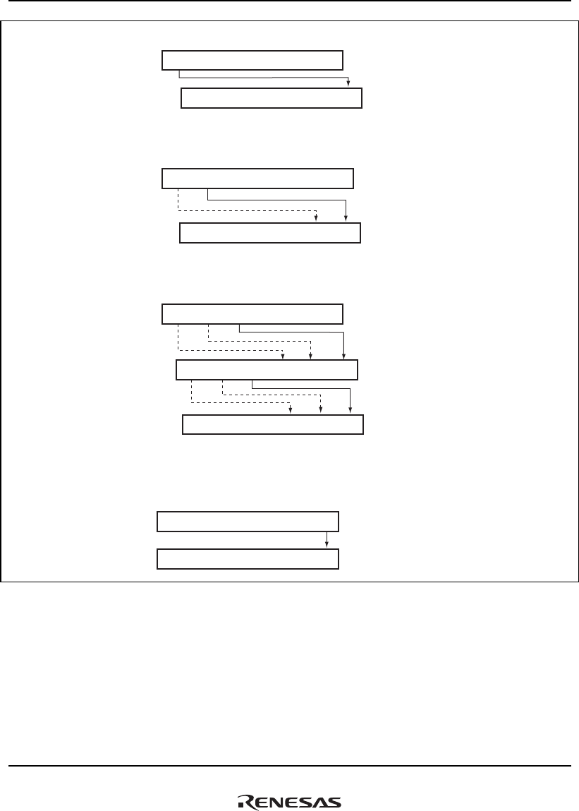
14. Direct Memory Access Controller (DMAC)
Rev.1.00 Jan. 10, 2008 Page 707 of 1658
REJ09B0261-0100
CH1 > CH2 > CH3 > CH4 > CH5 > CH0
CH0 > CH1 > CH2 > CH3 > CH4 > CH5
CH2 > CH3 > CH4 > CH5 > CH0 > CH1
CH0 > CH1 > CH2 > CH3 > CH4 > CH5
CH0 > CH1 > CH2 > CH3 > CH4 > CH5
CH0 > CH1 > CH2 > CH3 > CH4 > CH5
CH0 > CH1 > CH2 > CH3 > CH4 > CH5
CH3 > CH4 > CH5 > CH0 > CH1 > CH2
CH0 > CH1 > CH2 > CH3 > CH4 > CH5
(1) When channel 0 transfers
Initial priority order
Initial priority order
Initial priority order
Initial priority order
Priority order
after transfer
Priority order does not change.
Channel 2 becomes bottom
priority.
The priority of channels 0 and 1,
which were higher than channel 2,
are also shifted. If immediately
after there is a request to transfer
channel 5 only, channel 5 becomes
bottom priority and the priority of
channels 3 and 4, which were
higher than channel 5, are also
shifted.
Channel 1 becomes bottom
priority.
The priority of channel 0, which
was higher than channel 1, is also
shifted.
Channel 0 becomes bottom
priority
Priority order
after transfer
Priority order
after transfer
Priority order
after transfer
Post-transfer priority order
when there is an
immediate transfer
request to channel 5 only
(2) When channel 1 transfers
(3) When channel 2 transfers
(4) When channel 5 transfers
Figure 14.2 Round-Robin Mode (Example of Channels 0 to 5)
14. Direct Memory Access Controller (DMAC)
Rev.1.00 Jan. 10, 2008 Page 708 of 1658
REJ09B0261-0100
Figure 14.3 shows how the priority changes when channel 0 and channel 3 transfers are requested
simultaneously and a channel 1 transfer is requested during the channel 0 transfer. The DMAC
operates as follows:
1. Transfer requests are generated simultaneously to channels 0 and 3.
2. As channel 0 has a higher priority, the channel 0 transfer starts (channel 3 is waiting for
transfer).
3. A channel 1 transfer request occurs during the channel 0 transfer (channels 1 and 3 are waiting
for transfer).
4. When the channel 0 transfer ends, channel 0 has the lowest priority.
5. As channel 1 has a higher priority than channel 3 at this point, the channel 1 transfer starts
(channel 3 is waiting for transfer).
6. When the channel 1 transfer ends, channel 1 has the lowest priority.
7. The channel 3 transfer starts.
8. When the channel 3 transfer ends, channels 3 and 2 have lower priority so that channel 3 has
the lowest priority.
Transfer request Waiting channel(s) DMAC operation Channel priority
(1) Channels 0 and 3
(3) Channel 1
0 > 1 > 2 > 3 > 4 > 5(2) Channel 0 transfer
start
(4) Channel 0 transfer
ends
(5) Channel 1 transfer
starts
(6) Channel 1 transfer
ends
(7) Channel 3 transfer
starts
(8) Channel 3 transfer
ends
1 > 2 > 3 > 4 > 5 > 0
2 > 3 > 4 > 5 > 0 > 1
4 > 5 > 0 > 1 > 2 > 3
Priority order
changes
Priority order
changes
Priority order
changes
None
3
3
1,3
Figure 14.3 Changes in Channel Priority in Round-Robin Mode
(Example of Channels 0 to 5)

14. Direct Memory Access Controller (DMAC)
Rev.1.00 Jan. 10, 2008 Page 709 of 1658
REJ09B0261-0100
14.4.3 DMA Transfer Types
Tables 14.9 and 14.10 show the transfer directions that can be supported by the DMAC.
DMA transfer type supports dual address mode. A data transfer timing depends on the bus mode.
Bus modes include cycle steal mode and burst mode.
Table 14.9 DMA Transfer Directions for Auto-Request and External Request*2
Transfer Destination
Transfer Source
LBSC
Space
DBSC
Space PCIC Space
On-Chip
Peripheral
Module*1
L or U
Memory
LBSC Space Y Y Y Y Y
DBSC Space Y Y Y Y Y
PCIC Space Y Y Y Y Y
On-Chip Peripheral
Module*1
Y Y Y Y Y
L or U Memory Y Y Y Y Y
Legend:
Y: Transfer is enabled.
Notes: 1. This is the access size that is permitted by a register when the transfer source or
destination is a peripheral module.
2. External requests apply to only channels 0 to 3.

14. Direct Memory Access Controller (DMAC)
Rev.1.00 Jan. 10, 2008 Page 710 of 1658
REJ09B0261-0100
Table 14.10 DMA Transfer Directions for On-Chip Peripheral Module Request*2*3
Transfer Destination
Transfer Source
LBSC
Space
DBSC
Space PCIC Space
On-Chip
Peripheral
Module*1
L or U
Memory
LBSC Space N N N Y N
DBSC Space N N N Y N
PCIC Space N N N Y N
On-Chip Peripheral
Module*1
Y Y Y Y Y
L or U Memory N N N Y N
Legend:
Y: Transfer is enabled.
N: Transfer is disabled.
Notes: 1. This is the access size that is permitted by a register when the transfer source or
destination is an on-chip peripheral module.
2. The transfer source or destination must be the request source register for an on-chip
peripheral module request.
3. Only cycle steal mode can be set.
14. Direct Memory Access Controller (DMAC)
Rev.1.00 Jan. 10, 2008 Page 711 of 1658
REJ09B0261-0100
(1) Dual Address Mode
In dual address mode, both the transfer source and transfer destination are accessed by address.
The source and destination can be specified externally or internally. Data is read from the transfer
source in a data read cycle and written to the transfer destination in a data write cycle, and two bus
cycles are required to execute DMA transfer. At this time, transfer data is temporarily stored in the
DMAC. In the transfer between external memories shown in figure 14.4, data is read from an
external memory to the DMAC in a data read cycle, and then the data is written to the other
external memory in a write cycle.
Figure 14.5 shows the DMA transfer timing in dual address mode.
Data buffer
Address bus
Data bus
Address bus
Data bus
Memory
Transfer source
module
Transfer destination
module
Memory
Transfer source
module
Transfer destination
module
SAR
DAR
Data buffer
SAR
DAR
The SAR value is an address, data is read from the transfer source module,
and the data is temporarily stored in the DMAC.
First bus cycle
Second bus cycle
The DAR value is an address and the value stored in the data buffer in the
DMAC is written to the transfer destination module.
DMAC
DMAC
Figure 14.4 Data Flow of Dual Address Mode
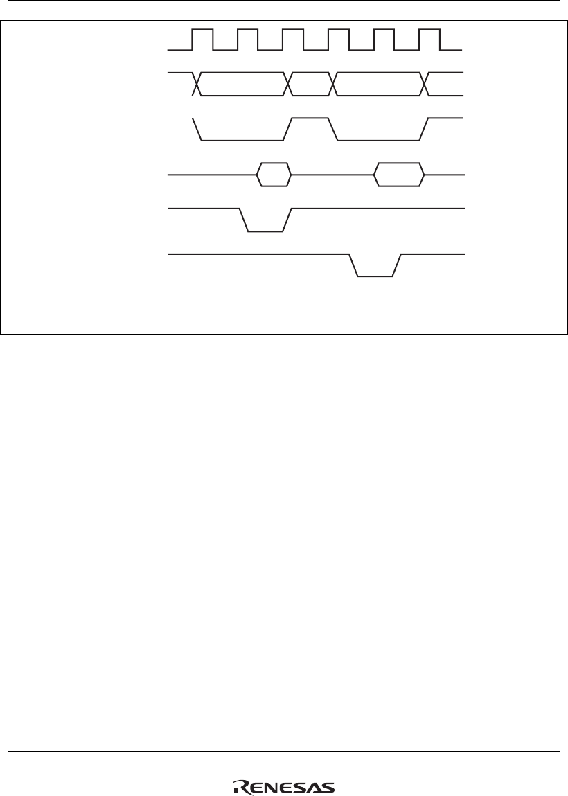
14. Direct Memory Access Controller (DMAC)
Rev.1.00 Jan. 10, 2008 Page 712 of 1658
REJ09B0261-0100
Transfer
source address Transfer
destination address
CLKOUT
A25 to A0
CSn
RD
WEn
D31 to D0
DACKn
(Active-low)
Figure 14.5 Example of DMA Transfer Timing in Dual Address Mode
(Source: SRAM, Destination: DDR-SDRAM)
14. Direct Memory Access Controller (DMAC)
Rev.1.00 Jan. 10, 2008 Page 713 of 1658
REJ09B0261-0100
(2) Bus Modes
Bus modes include cycle steal mode and burst mode. The modes are chosen by the TB and LCKN
bits in CHCR.
(a) Cycle Steal Mode
• Normal mode 1 (CHCR.LCKN = 0, CHCR.TB = 0)
In cycle steal normal mode 1, the DMAC gives the SuperHyway bus mastership to another bus
master after a one-transfer unit (byte, word, longword, 16-byte, or 32-byte unit). When the
next transfer is requested, the DMAC issues the next transfer request, another transfer is
performed for one-transfer unit. When the transfer ends, the DMAC gives bus mastership to
the other bus master. This is repeated until the transfer end conditions are satisfied.
Cycle steal normal mode 1 can be set for only channels 0 to 5.
Figure 14.6 shows an example of DMA transfer timing in cycle steal normal mode 1.
DREQ
SuperHyway
bus cycle
Bus mastership returned to CPU once
Read/Write Read/Write
CPU CPU CPU DMAC DMAC CPU DMAC DMAC CPU
Figure 14.6 DMA Transfer Timing Example in Cycle Steal Normal Mode 1
(DREQ Low Level Detection)
• Normal mode 2 (CHCR.LCKN = 1, CHCR.TB = 0)
In cycle steal normal mode 2, the DMAC does not keep the SuperHyway bus mastership, and
obtains the bus mastership in every transfer unit of read or write cycle.
Figure 14.7 shows an example of DMA transfer timing in cycle steal normal mode 2.
SuperHyway
bus cycle
Bus mastership returned to CPU once
Read Write Read Write
CPU CPUDMAC DMAC CPU DMAC DMACCPU CPUCPUCPU
DREQ
Figure 14.7 DMA Transfer Timing Example in Cycle Steal Normal Mode 2
(DREQ Low Level Detection)
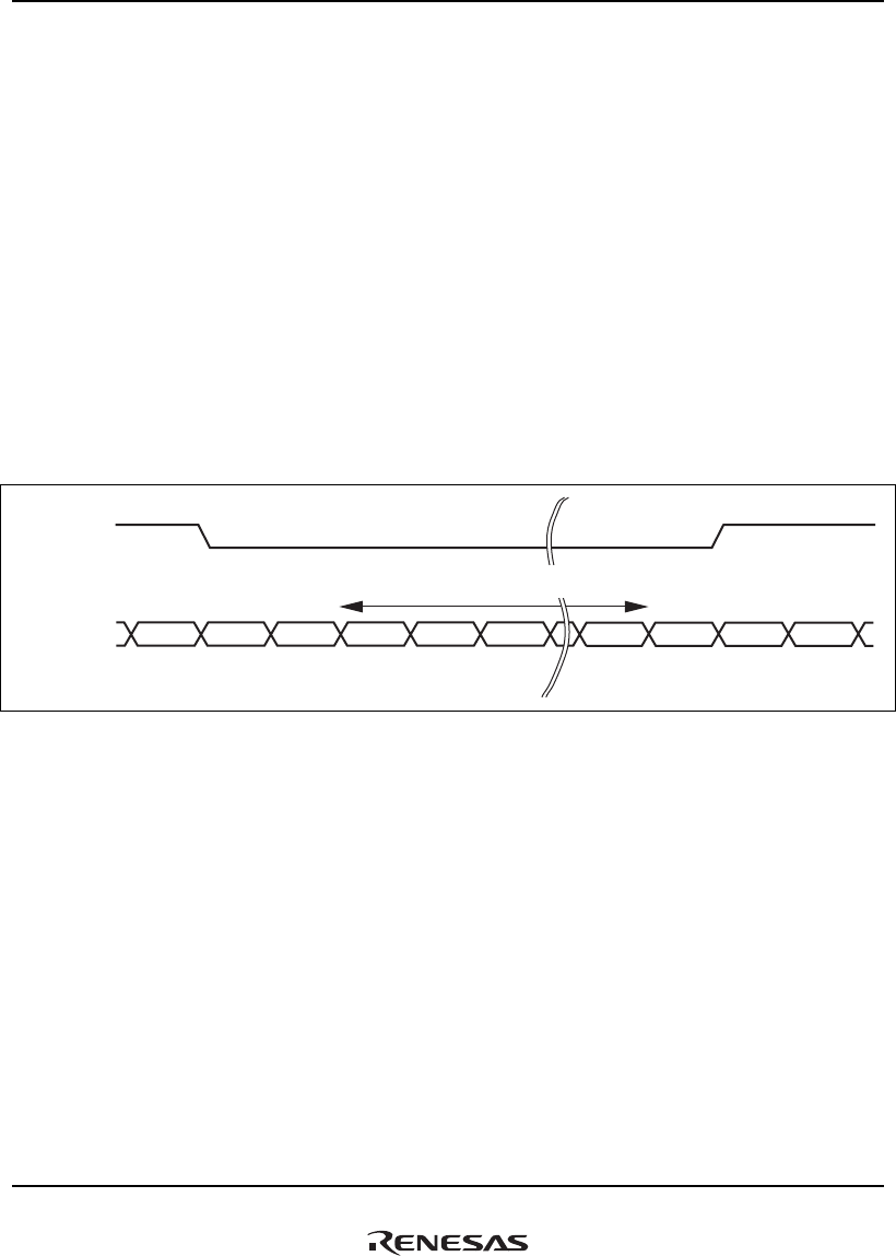
14. Direct Memory Access Controller (DMAC)
Rev.1.00 Jan. 10, 2008 Page 714 of 1658
REJ09B0261-0100
• Intermittent mode 16 (DMAOR. CMS = 10, CHCR.LCKN = 0 or 1, CHCR.TB = 0)
• Intermittent mode 64 (DMAOR. CMS = 11, CHCR.LCKN = 0 or 1, CHCR.TB = 0)
In intermittent mode of cycle steal, the DMAC gives the SuperHyway bus mastership to other
bus master whenever a one-transfer unit (byte, word, longword, or 16-byte or 32-byte unit) is
completed. After that, if the next transfer request occurs, the DMAC issues the next transfer
request after waiting for 16 or 64 clocks in Bck, transfers data of one-transfer unit again, and
returns the SuperHyway bus mastership to other bus master. These operations are repeated
until the transfer end condition is satisfied. It is possible to make lower the ratio of bus
occupation by DMA transfer than cycle steal normal modes 1 and 2.
When the DMAC issues the next transfer request again, DMA transfer can be postponed in
case of entry updating due to cache miss.
The intermittent modes must be cycle steal mode in all channels (channels 0 to 5)
corresponding to DMAOR0 or all channels (channels 6 to11) corresponding to DMAOR1.
Figure 14.8 shows an example of DMA transfer timing in cycle steal intermittent mode.
DREQ
SuperHyway
bus cycle
Read/Write Read/Write
CPU CPU CPU DMAC DMAC CPU CPU DMAC DMAC CPU
More than 16 or 64 Bck
(depends on DMAOR.CMS settings)
Figure 14.8 Example e of DMA Transfer Timing in Cycle Steal Intermittent Mode
(DREQ Low Level Detection)
(b) Burst Mode (CHCR.LCKN = 1, CHCR.TB = 1)
In burst mode, once the DMAC obtains the SuperHyway bus mastership, the transfer is performed
continuously without releasing the bus mastership until the transfer end condition is satisfied. If
the DREQ is detected at level in external request mode, when the DREQ pin is not active, the
DMAC passes bus mastership to the other bus master after the DMAC transfer request that has
already been accepted ends, even if the transfer end conditions have not been satisfied.
Burst mode is not available when an on-chip peripheral module is the transfer request source.
Burst mode can be set for only channels 0 to 5.
Figure 14.9 shows DMA transfer timing in burst mode.
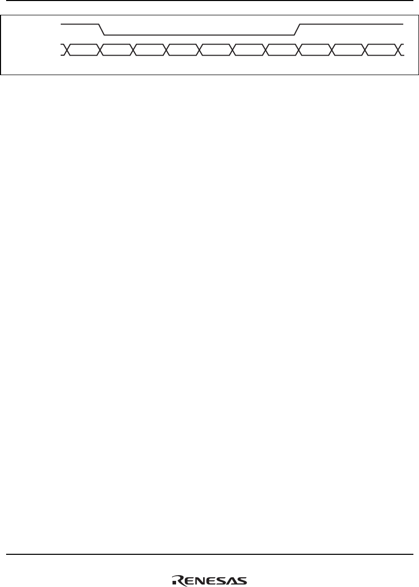
14. Direct Memory Access Controller (DMAC)
Rev.1.00 Jan. 10, 2008 Page 715 of 1658
REJ09B0261-0100
SuperHyway
bus cycle
Read Write Read Write Read Write
DREQ
CPU CPU CPU DMAC DMAC DMAC DMAC DMAC DMAC CPU
Figure 14.9 DMA Transfer Timing Example in Burst Mode
(DREQ Low Level Detection)
(3) Bus Mode and Channel Priority
Figure 14.10 shows the bus modes and channel priority in priority fixed mode.
In priority fixed mode (CH0 > CH1), when channel 1 is transferring in burst mode, the transfer of
channel 0 starts immediately if there is a transfer request to channel 0 with a higher priority.
At this time, if channel 0 is also in burst mode, the channel 1 transfer continues after the channel 0
transfer has completely ended. (Figure 14.10 (h))
When channel 0 is in cycle steal mode, channel 0 with a higher priority performs the transfer of
one transfer unit and the channel 1 transfer is continuously performed without releasing the bus
mastership. The bus mastership then switches between the two in the order channel 0, channel 1,
channel 0, and channel 1. (Figure 14.10 (d))
In other words, the bus status looks as if the CPU cycle reached after the transfer in cycle steal
mode is replaced with transfer in burst mode (the status is called "burst mode priority execution").
When multiple channels are operating in burst modes, the channel with the highest priority is
executed first.
When DMA transfer is executed in the multiple channels, the bus mastership is not given to the
bus master until all competing burst transfers are completed.
In round-robin mode, the priority changes according to the specification shown in figure 14.3.
However, the channel in cycle steal mode and the channel in burst mode cannot be mixed.
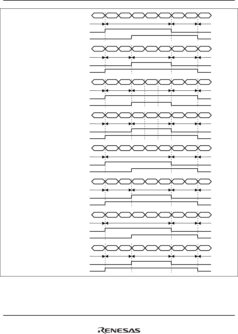
14. Direct Memory Access Controller (DMAC)
Rev.1.00 Jan. 10, 2008 Page 716 of 1658
REJ09B0261-0100
DMA CH0
Cycle steal
CH0 transfer source
(a) CH0: Cycle steal mode
CH1: Cycle steal mode
Priority: CH0 > CH1
CPU DMA CH1DMA CH0 DMA CH0 DMA CH0 DMA CH0 DMA CH0 DMA CH1 CPU
DMA CH1
Cycle steal
CH1 transfer source
DMA CH0
Cycle steal
CH1 transfer source
CH0 transfer source
CPU DMA CH0DMA CH0 DMA CH0 DMA CH1 DMA CH0 DMA CH1 DMA CH0
DMA CH0
Cycle steal
CPU
DMA CH0 and CH1
Burst mode
DMA CH1
Cycle steal
CH1 transfer source
CH0 transfer source
CPU DMA CH1DMA CH1 DMA CH1 DMA CH0 DMA CH0 DMA CH0 DMA CH1
DMA CH1
Cycle steal
CPU
DMA CH0
Cycle steal
DMA CH1
Cycle steal
CH1 transfer source
CH0 transfer source
CPU DMA CH1DMA CH1 DMA CH1 DMA CH0 DMA CH0 DMA CH0 DMA CH1
DMA CH1
Cycle steal
CPU
DMA CH0
Burst mode
DMA CH1
Burst mode
CH1 transfer source
CH0 transfer source
CPU DMA CH1DMA CH1 DMA CH1 DMA CH0 DMA CH1 DMA CH0 DMA CH1
DMA CH1
Burst mode
CPU
DMA CH0 and CH1
Burst mode
DMA CH0
Burst mode
CH1 transfer source
CH0 transfer source
CPU DMA CH1DMA CH0 DMA CH0 DMA CH0 DMA CH DMA CH0 DMA CH1
DMA CH1
Cycle steal
CPU
DMA CH0
Burst mode
CH1 transfer source
CH0 transfer source
CPU DMA CH1DMA CH0 DMA CH0 DMA CH0 DMA CH0 DMA CH0 DMA CH1
DMA CH1
Burst mode
CPU
DMA CH1
Burst mode
CH1 transfer source
CH0 transfer source
CPU DMA CH1DMA CH1 DMA CH1 DMA CH0 DMA CH0 DMA CH0 DMA CH1
DMA CH1
Burst mode
CPU
DMA CH0
Burst mode
(b) CH0: Cycle steal mode
CH1: Cycle steal mode
Priority: CH0 > CH1
(d) CH0: Cycle steal mode
CH1: Burst mode
Priority: CH0 > CH1
(e) CH0: Burst mode
CH1: Cycle steal mode
Priority: CH0 > CH1
(f) CH0: Burst mode
CH1: Cycle steal mode
Priority: CH0 > CH1
(g) CH0: Burst mode
CH1: Burst mode
Priority: CH0 > CH1
(h) CH0: Burst mode
CH1: Burst mode
Priority: CH0 > CH1
(c) CH0: Cycle steal mode
CH1: Burst mode
Priority: CH0 > CH1
Figure 14.10 Bus Mode and Channel Priority in Priority Fixed Mode

14. Direct Memory Access Controller (DMAC)
Rev.1.00 Jan. 10, 2008 Page 717 of 1658
REJ09B0261-0100
14.4.4 DMA Transfer Flow
After intended transfer conditions are set to SAR, DAR, TCR, CHCR, DMAOR, and DMARS, the
DMAC transfers data according to the following procedure.
1. Checks if transfer is enabled (DE = 1, DME = 1, TE = 0, AE = 0, NMIF = 0)
2. When a transfer request occurs while transfer is enabled, the DMAC transfers one transfer unit
of data (depending on the settings of TS0, TS1, and TS2). In auto-request mode, the transfer
starts automatically when the DE and DME bits are set to 1. The TCR is decremented for each
transfer. The actual transfer flows depend on address mode and bus mode.
3. When the specified number of transfers has been completed (when TCR is 0), the transfer ends
successfully. If the IE bit in CHCR is set to 1 at this time, a DMINT interrupt is sent to the
CPU.
4. When an address error or an NMI interrupt is generated by the DMAC, the transfer is aborted.
Transfers are also aborted when the DE bit in CHCR or the DME bit in DMAOR is cleared to
0.
Figure 14.11 shows a flowchart of DMA transfer.
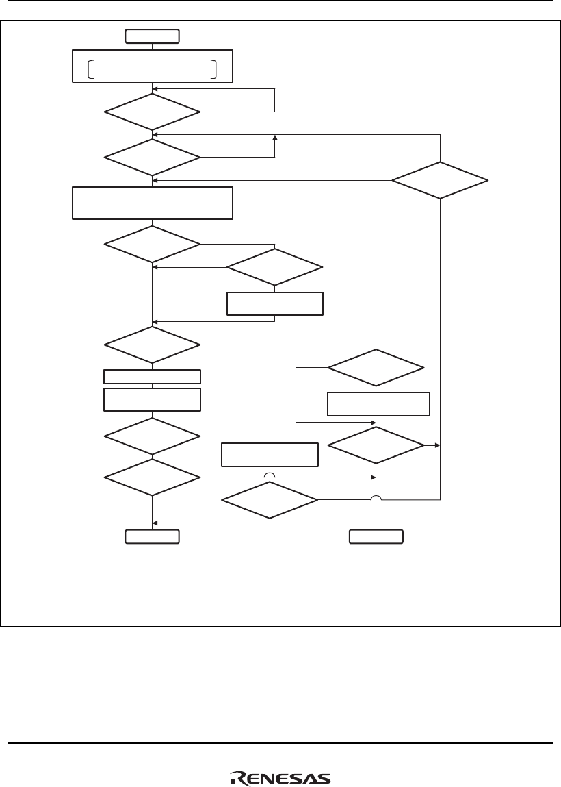
14. Direct Memory Access Controller (DMAC)
Rev.1.00 Jan. 10, 2008 Page 718 of 1658
REJ09B0261-0100
Notes: 1. In repeat mode, a transfer request is acceptted with TE =1 when HIE = 1 and HE = 0
(half end interrupt is enable and clear the HE to 0 after HE is set to 1).
2. In auto-request mode, transfer starts when bits NMIF, AE, and TE are all 0 or bits TE
and HIE are 1 and HE is 0 (in repeat mode), and bits DE and DME are set to 1.
3. DREQ is level detection (external request) in burst mode or cycle-steral mode.
4. DREQ is edge detection (external request) or auto request in burst mode.
5. Loading to SAR and DAR differs according to the operating conditions in each mode.
6. TCRBH and TCRBL refer to TCRB23 to TCRB16 and TCRB7 to TCRB0 respectively.
NMIF = 1 or AE =1 or
DE = 0 or DME = 0?
Normal end Transfer end
NMIF = 1 or AE = 1 or
DE = 0 or DME = 0?
SARB/DARB load
TCRB
→ TCR load
HIE = 0 or HE = 1?
Yes Yes
No
No
*
5
No
Yes
TCR = 0?
TE = 1
DMINT interrupt request
(IE = 1)
Repeat mode?
TCR = TCRB/2?
HE = 1, DMINT interrupt
request (HIE = 1)
Yes
Yes
Yes
No
No
No
Transfer (1 transfer unit);
TCR – 1 → TCR, SAR, and DAR updated
Reload mode:
TCRBL – 1 → TCRBL
Reload mode?
TCRBL = 0?
SARB/DARB load
TCRBH → TCRBL load
Bus mode, DREQ
detection system,
transfer request mode
Yes
No
*
5
Yes
No
*
6
*
6
Start
Initial settings
SAR, DAR, TCR, CHCR, DMAOR
SARB, DARB, TCRB, DMARS
DE, DME = 1 and
TE, AE, NMIF = 0?
Transfer request occurs?
No
No
*
1
*
2
*
3
*
4
Yes
Yes
Figure 14.11 Flowchart of DMA Transfer

14. Direct Memory Access Controller (DMAC)
Rev.1.00 Jan. 10, 2008 Page 719 of 1658
REJ09B0261-0100
14.4.5 Repeat Mode Transfer
A repeat mode transfer of the DMAC enables a DMA transfer to repeat without specifying the
transfer settings before a transfer.
Using a repeat mode transfer with the half end function can execute a double buffer transfer
virtually. This function can execute the following procedures efficiently. As an example, the
operation in receiving voice data from the VOICE CODEC and compressing the data is described.
The process described supposes that processing of compressing is executed whenever 40-word
voice data is received. Suppose that voice data is received by SIOF.
1. DMAC settings
⎯ Set the address of the SIOF receive data register in SAR
⎯ Set the address of an internal memory data store area in DAR
⎯ Set TCR to H'50 (80 times)
⎯ Set the following values to CHCR
RPT (bits 27 to 25) = B'010: Repeat mode (use DAR as a repeat area)
HIE (bit 18) = B'1: TCR/2 interrupt generated
DM (bits 15 and 14) = B'01: DAR incremented
SM (bits 13 and 12) = B'00: SAR fixed
IE (bit 2) = B'1: Interrupt enabled
DE (bit 0) = B'1: DMA transfer enabled
Set bits such as bits TB and TS according to use conditions
⎯ Set bits CMS and PR in DMAOR according to use conditions and set the DME bit to 1
2. Voice data is received and transferred by SIOF/DMAC
3. TCR is decreased to half of the initial value and an interrupt is generated
After reading CHCR and confirming that the HE (bit 19) is set to 1 by an interrupt processing,
clear HE (bit 19) to 0 and compress 40-word voice data from the address set in DAR.
4. TCR is cleared to 0 and an interrupt is generated
After reading CHCR and confirming that the TE bit is set to 1 with an interrupt processing,
clear the TE bit to 0 and compress 40-word voice data from the address that is obtained by
adding 40 to the address set in DAR. After this operation, the value of DARB is copied to
DAR in DMAC and initialized, and the value of TCRB is copied to TCR and initialized to
H'50 (80 times).
5. Steps 2 to 4 are repeated until the DME or DE bit is set to B'0, or an NMI interrupt is
generated. (If the HE bit is not cleared to 0 in the procedure 2 or if the TE bit is not cleared to 0
in the procedure 4, the transfer is stopped when both the HE and TE bits are set to 1.)

14. Direct Memory Access Controller (DMAC)
Rev.1.00 Jan. 10, 2008 Page 720 of 1658
REJ09B0261-0100
This function enables sequential voice compression by switching a storing buffer for data received
consequentially and a data buffer for processing signals alternately.
14.4.6 Reload Mode Transfer
In a reload mode transfer, according to the settings of bits RPT in CHCR, the value set in
SARB/DARB is reloaded to SAR/DAR at each transfer set in bits 23 to 16 and bits 7 to 0 in
TCRB, and the transfer is repeated until TCR is 0 without specifying the transfer again. This
function is effective when data transfer with specific area is repeatedly executed. Figure 14.12
shows the operation of reload mode transfer.
In reload mode, TCRB is used as a reload counter. See section 14.3.6, DMA Transfer Count
Registers B0 to B3, B6 to B9 (TCRB0 to TCRB3, TCRB6 to TCRB9), and set TCRB.
Figure 14.12 shows an example of reload mode settings.
Register settings
Set the source address in SAR (the data written to SAR is also written to SARB.)
Set the destination address in DAR
Set H'0000000C to TCR (12 transfers)
Set H'00040004 to TCRB (Reloading for every four transfers)
Set CHCR as follows.
RPT (bits 27 to 25) = B'111: Reload mode (Reloading SAR)
DM (bits 15 to 14) = B'01: An increase in DAR
SM (bits 13 to 12) = B'01: An increase in SAR
TS (bit 20 and bits 4 to 3) = B'010: Transfer for each (four-byte) longword
DMA transfer source addresses and DMA transfer destination addresses in the above register settings
Cycle 1: Source address = SAR Destination address = DAR
Cycle 2: Source address = SAR + H'04 Destination address = DAR + H'04
Cycle 3: Source address = SAR + H'08 Destination address = DAR + H'08
Cycle 4: Source address = SAR + H'0C Destination address = DAR + H'0C
Cycle 5: Source address = SAR Destination address = DAR + H'10 (reloading the value of SARB in SAR)
Cycle 6: Source address = SAR + H'04 Destination address = DAR + H'14
Cycle 7: Source address = SAR + H'08 Destination address = DAR + H'18
Cycle 8: Source address = SAR + H'0C Destination address = DAR + H'1C
Cycle 9: Source address = SAR Destination address = DAR + H'20 (reloading the value of SARB in SAR)
Cycle 10: Source address = SAR + H'04 Destination address = DAR + H'24
Cycle 11: Source address = SAR + H'08 Destination address = DAR + H'28
Cycle 12: Source address = SAR + H'0C Destination address = DAR + H'2C
The relationship between the register settings and the source and destination addresses
of reload mode transfer is described below.
Figure 14.12 Example of Operation Based on Reload Mode Settings
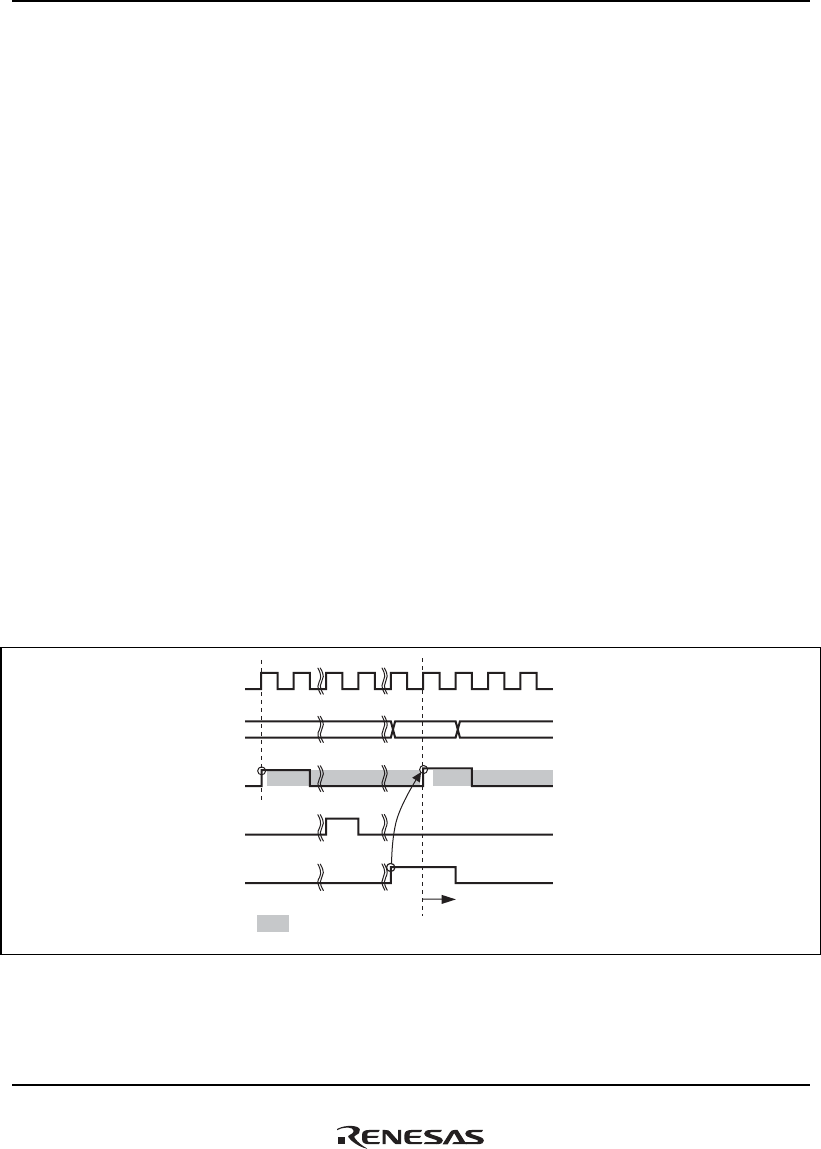
14. Direct Memory Access Controller (DMAC)
Rev.1.00 Jan. 10, 2008 Page 721 of 1658
REJ09B0261-0100
14.4.7 DREQ Pin Sampling Timing
Figures 14.13 to 14.22 show the timing that the DREQ input is sampled in each bus mode.
Figures 14.13, 14.16, and 14.20 show the timing that the DREQ input is sampled when byte
transfer is performed in 8-, 16-, 32-, or 64-bit bus width, word transfer is performed in 16-, 32-, or
64-bit bus width, or longword transfer is performed in 32- or 64-bit bus width. DACK is output
once in DMA1 transfer.
Figures 14.14, 14.17, and 14.21 show the timing that the DREQ input is sampled when word
transfer is performed in 8-bit bus width, longword transfer is performed in 8- or 16-bit bus width,
or 16- or 32-byte transfer is performed in 8-, 16-, 32-, or 64-bit bus width. These figures suppose
that DACK of DMA1 transfer is divided.
Figures 14.15, 14.18, and 14.22 show the timing that the DREQ input is sampled when word
transfer is performed in 8-bit bus width, longword transfer is performed in 8- or 16-bit bus width,
or 16- or 32-byte transfer is performed in 8-, 16-, 32-, or 64-bit bus width. These figures suppose
that DACK of DMA1 transfer is connected.
When word transfer is performed in 8-bit bus width, longword transfer is performed in 8- or 16-bit
bus width, or 16- or 32-byte transfer is performed in 8-, 16-, 32-, or 64-bit bus width, DMA
transfer units are divided into multiple bus cycles. If DMA transfer size is divided into multiple
bus cycles and CS is negated between bus cycles, DACK output is divided, like CS. For details,
see section 11.5.16, Register Settings for Divided-Up DACKn Output.
CLKOUT
Bus cycle
DREQ
(Rising edge)
DRAK
(High-active)
DACK
(High-active)
: Non-sensitive period
Accepted after one cycle of CLKOUT
at the rising edge of DACK
CPU DMAC CPU
1st acceptance 2nd acceptance
Acceptance started
Figure 14.13 Example 1 of DREQ Input Detection in Cycle Steal Mode Edge Detection
(Byte Transfer in 8/16/32/64-Bit Bus Width, Word Transfer in 16/32/64-Bit Bus Width, or
Longword Transfer in 32/64-Bit Bus Width)
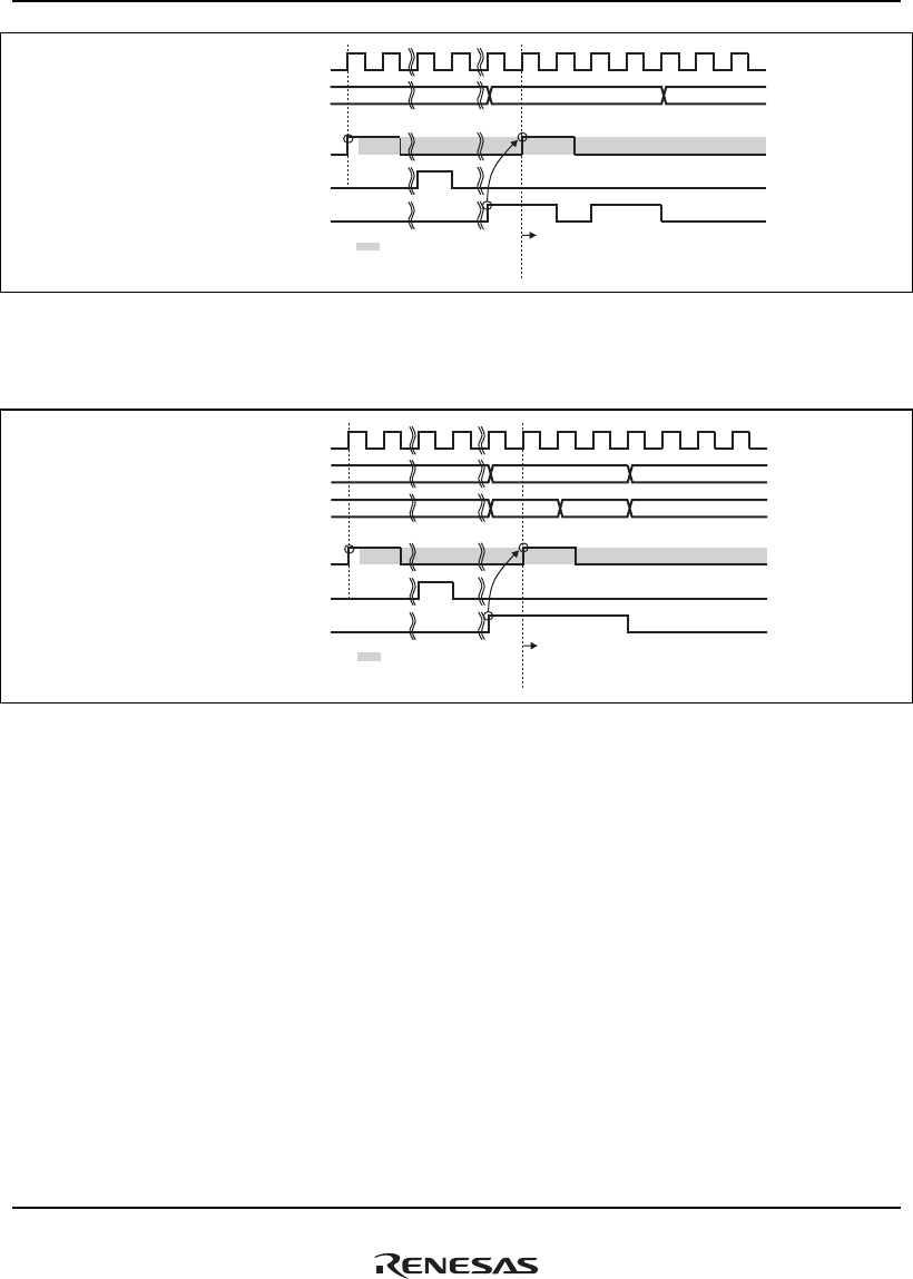
14. Direct Memory Access Controller (DMAC)
Rev.1.00 Jan. 10, 2008 Page 722 of 1658
REJ09B0261-0100
: Non-sensitive period
CLKOUT
Bus cycle
DREQ
(Rising edge)
DRAK (High-active)
DACK (High-active)
Acceptance started
Accepted after one cycle of CLKOUT
at the first rising edge of the divided-up DACK
1st acceptance 2nd acceptance
CPU CPUDMAC
Figure 14.14 Example 2 of DREQ Input Detection in Cycle Steal Mode Edge Detection
(Word Transfer in 8-Bit Bus Width, Longword Transfer in 8/16-Bit Bus Width, 16/32-Byte
Transfer in 8/16/32/64-Bit Bus Width: DACK of DMA1 Transfer Divided)
: Non-sensitive period
CLKOUT
Bus cycle
Address
DREQ (Rising edge)
DRAK (High-active)
DACK (High-active)
Acceptance started
Accepted after one cycle of CLKOUT
at the rising edge of DACK
1st acceptance 2nd acceptance
CPU CPUDMAC
Figure 14.15 Example 3 of DREQ Input Detection in Cycle Steal Mode Edge Detection
(Word Transfer in 8-Bit Bus Width, Longword Transfer in 8/16-Bit Bus Width, or 16/32-
Byte Transfer in 8/16/32/64-Bit Bus Width: DACK of DMA1 Transfer Is Connected)
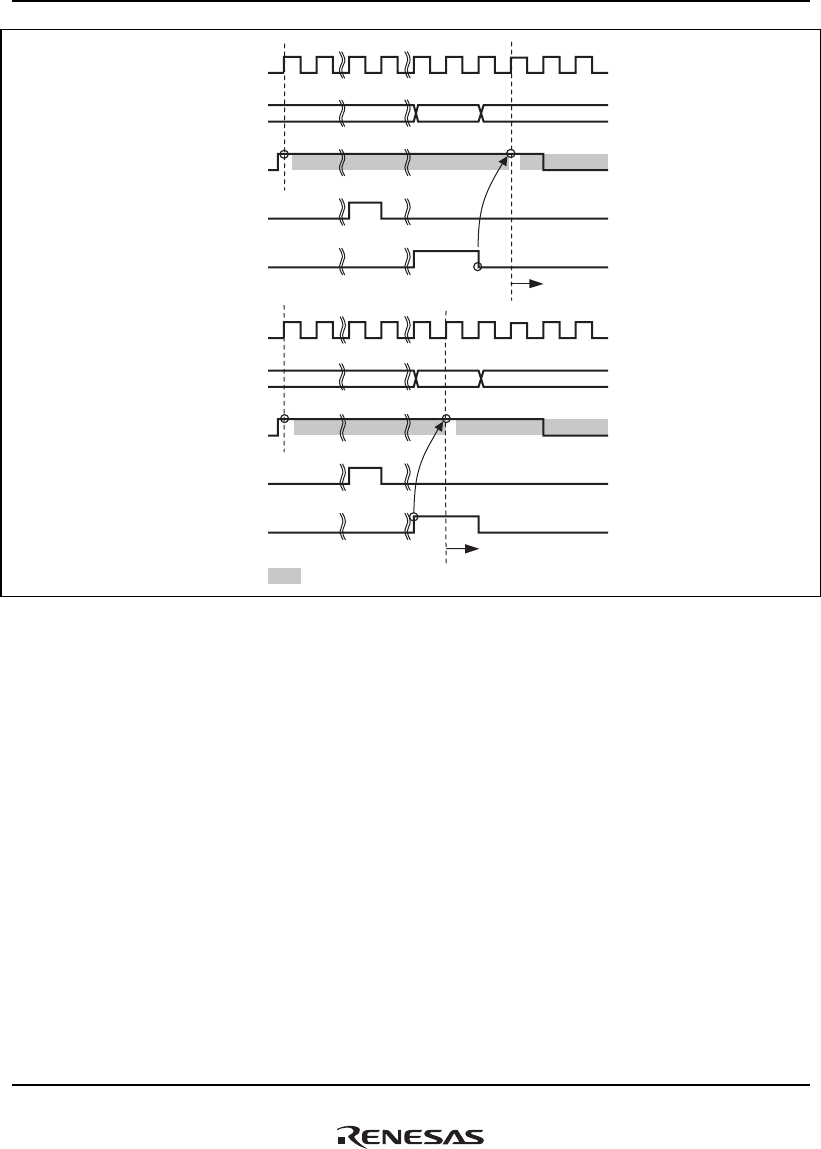
14. Direct Memory Access Controller (DMAC)
Rev.1.00 Jan. 10, 2008 Page 723 of 1658
REJ09B0261-0100
CLKOUT
Bus cycle
DREQ
(
Overrun 0, High level)
DRAK
(High-active)
DACK
(High-active)
CLKOUT
Bus cycle
DREQ
(
Overrun 1, High level)
DRAK
(High-active)
DACK
(High-active)
CPU DMAC CPU
1st acceptance
Acceptance started
Accepted after one cycle of CLKOUT
at the falling edge of DACK
: Non-sensitive period
1st acceptance
Acceptance started
Accepted after one cycle of CLKOUT
at the rising edge of DACK
CPU DMAC CPU
2nd acceptance
2nd acceptance
Figure 14.16 Example 1 of DREQ Input Detection in Cycle Steal Mode Level Detection
(Byte Transfer in 8/16/32/64-Bit Bus Width, Word Transfer in 16/32/64-Bit Bus Width, or
Longword Transfer in 32/64-Bit Bus Width)
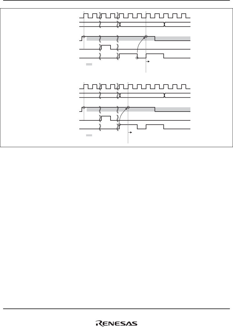
14. Direct Memory Access Controller (DMAC)
Rev.1.00 Jan. 10, 2008 Page 724 of 1658
REJ09B0261-0100
Bus cycle
DREQ
(
Overrun 0, High level)
DRAK (High-active)
DACK (High-active)
Bus cycle
DREQ
(
Overrun 1, High level)
DRAK (High-active)
DACK (High-active)
: Non-sensitive period
CLKOUT
Acceptance started
Accepted after one cycle of CLKOUT
at the first falling edge of the divided-up DACK
1st acceptance 2nd acceptance
CPU CPUDMAC
: Non-sensitive period
CLKOUT
Acceptance started
Accepted after one cycle of CLKOUT
at the first rising edge of the divided-up DACK
1st acceptance 2nd acceptance
CPU CPUDMAC
Figure 14.17 Example 2 of DREQ Input Detection in Cycle Steal Mode Level Detection
(Word Transfer in 8-Bit Bus Width, Longword Transfer in 8/16-Bit Bus Width, 16/32-Byte
Transfer in 8/16/32/64-Bit Bus Width: DACK of DMA1 Transfer Divided)
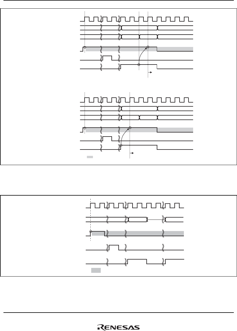
14. Direct Memory Access Controller (DMAC)
Rev.1.00 Jan. 10, 2008 Page 725 of 1658
REJ09B0261-0100
Acceptance started
Accepted after one cycle of CLKOUT
after the end of the first of the multiple bus cycles
1st acceptance 2nd acceptance
: Non-sensitive period
Acceptance started
Accepted after one cycle of CLKOUT
at the rising edge of DACK
1st acceptance 2nd acceptance
Bus cycle
DREQ
(
Overrun 0, High level)
DRAK (High-active)
DACK (High-active)
Bus cycle
DREQ
(
Overrun 1, High level)
DRAK (High-active)
DACK (High-active)
CLKOUT
Address
CPU CPU
DMAC
CLKOUT
Address
CPU CPUDMAC
Figure 14.18 Example 3 of DREQ Input Detection in Cycle Steal Mode Level Detection
(Word Transfer in 8-Bit Bus Width, Longword Transfer in 8/16-Bit Bus Width, or 16/32-
Byte Transfer in 8/16/32/64-Bit Bus Width: DACK of DMA1 Transfer Is Connected)
CLKOUT
CPU DMAC DMAC
Burst acceptance
: Non-sensitive period
Bus cycle
DREQ
(Rising edge)
DRAK
(High-active)
DACK
(High-active)
Figure 14.19 Example of DREQ Input Detection in Burst Mode Edge Detection
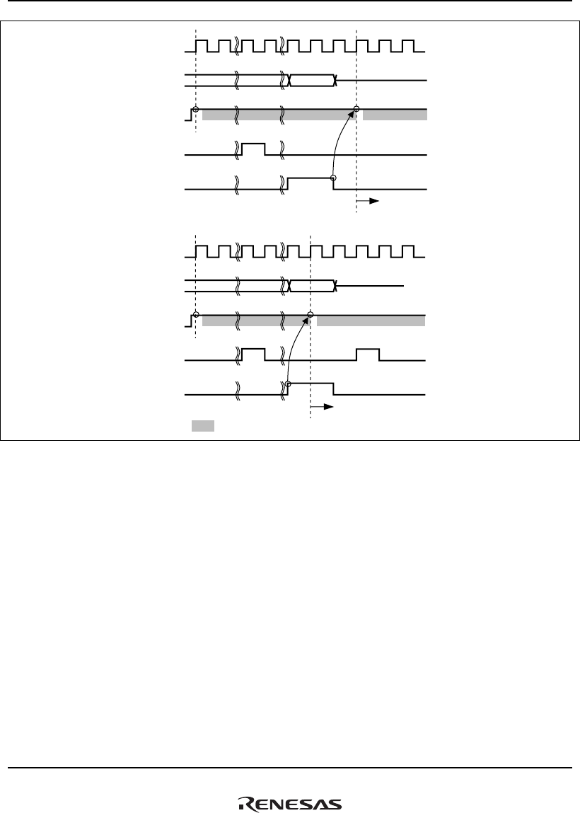
14. Direct Memory Access Controller (DMAC)
Rev.1.00 Jan. 10, 2008 Page 726 of 1658
REJ09B0261-0100
Bus cycle
(
Overrun 0, High level)
DRAK (High-active)
DACK (High-active)
Bus cycle
(
Overrun 1, High level)
DRAK (High-active)
DACK (High-active)
Acceptance started
Accepted after one cycle of CLKOUT
at the falling edge of DACK
1st acceptance 2nd acceptance
: Non-sensitive period
Acceptance started
Accepted after one cycle of CLKOUT
at the rising edge of DACK
1st acceptance 2nd acceptance
CLKOUT
DREQ
CLKOUT
DREQ
CPU DMAC
CPU DMAC
Figure 14.20 Example 1 of DREQ Input Detection in Burst Mode Level Detection (Byte
Transfer in 8/16/32/64-Bit Bus Width, Word Transfer in 16/32/64-Bit Bus Width, or
Longword Transfer in 32/64-Bit Bus Width)
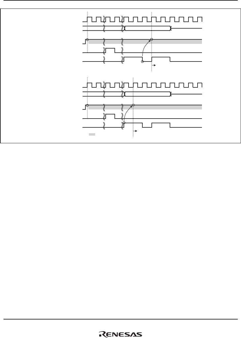
14. Direct Memory Access Controller (DMAC)
Rev.1.00 Jan. 10, 2008 Page 727 of 1658
REJ09B0261-0100
Acceptance started
Accepted after one cycle of CLKOUT
at the first falling edge of the divided-up DACK
1st acceptance 2nd acceptance
: Non-sensitive period
Acceptance started
Accepted after one cycle of CLKOUT
at the first rising edge of the divided-up DACK
1st acceptance 2nd acceptance
Bus cycle
DREQ
(
Overrun 0, High level)
DRAK (High-active)
DACK (High-active)
Bus cycle
DREQ
(
Overrun 1, High level)
DRAK (High-active)
DACK (High-active)
CLKOUT
CPU DMAC
CLKOUT
CPU DMAC
Figure 14.21 Example 2 of DREQ Input Detection in Burst Mode Level Detection (Word
Transfer in 8-Bit Bus Width, Longword Transfer in 8/16-Bit Bus Width, 16/32-Byte
Transfer in 8/16/32/64-Bit Bus Width: DACK of DMA1 Transfer Divided)
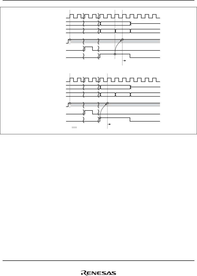
14. Direct Memory Access Controller (DMAC)
Rev.1.00 Jan. 10, 2008 Page 728 of 1658
REJ09B0261-0100
Acceptance started
Accepted after one cycle of CLKOUT
after the end of the first of the multiple bus cycles
1st acceptance 2nd acceptance
: Non-sensitive period
Acceptance started
Accepted after one cycle of CLKOUT
at the rising edge of DACK
1st acceptance 2nd acceptance
Bus cycle
DREQ
(
Overrun 0, High level)
DRAK (High-active)
DACK (High-active)
Bus cycle
DREQ
(
Overrun 1, High level)
DRAK (High-active)
DACK (High-active)
Address
Address
CLKOUT
CPU DMAC
CLKOUT
CPU DMAC
Figure 14.22 Example 3 of DREQ Input Detection in Burst Mode Level Detection (Word
Transfer in 8-Bit Bus Width, Longword Transfer in 8/16-Bit Bus Width, or 16/32-Byte
Transfer in 8/16/32/64-Bit Bus Width: DACK of DMA1 Transfer Is Connected)

14. Direct Memory Access Controller (DMAC)
Rev.1.00 Jan. 10, 2008 Page 729 of 1658
REJ09B0261-0100
14.5 DMAC Interrupt Sources
In the DMAC, each channel has 14 interrupt sources: a DMA transfer end/half-end interrupts
request (DMINT0 to DMINT11), a DMA address error interrupt request (DMAE0) common to
channels 0 to 5, and a DMA address error interrupt request (DMAE1) common to channels 6 to
11.
Table 14.11 shows each interrupt source. Each interrupt source is independently sent to the
interrupt controller.
Table 14.11 DMAC Interrupt Sources
Interrupt Factor Description
DMINT0 Channel 0 DMA transfer-end/half-end interrupt
DMINT1 Channel 1 DMA transfer-end/half-end interrupt
DMINT2 Channel 2 DMA transfer-end/half-end interrupt
DMINT3 Channel 3 DMA transfer-end/half-end interrupt
DMINT4 Channel 4 DMA transfer-end/half-end interrupt
DMINT5 Channel 5 DMA transfer-end/half-end interrupt
DMAE0 DMA address error interrupt common to channels 0 to 5
DMINT6 Channel 6 DMA transfer-end/half-end interrupt
DMINT7 Channel 7 DMA transfer-end/half-end interrupt
DMINT8 Channel 8 DMA transfer-end/half-end interrupt
DMINT9 Channel 9 DMA transfer-end/half-end interrupt
DMINT10 Channel 10 DMA transfer-end/half-end interrupt
DMINT11 Channel 11 DMA transfer-end/half-end interrupt
DMAE1 DMA address error interrupt common to channels 6 to 11

14. Direct Memory Access Controller (DMAC)
Rev.1.00 Jan. 10, 2008 Page 730 of 1658
REJ09B0261-0100
14.6 Usage Notes
Note the following things in using this DMAC.
14.6.1 Stopping Modules and Changing Frequency
When the DMAC is operating, it is prohibited to set or clear the corresponding bit of MSTPCR1
that controls H-UDI, UBC, DMAC and GDTA modules operation, and also prohibited to change
any frequencies regarding the operation of this LSI. Operation is not guaranteed if these are
performed.
Check that the DME bits (bit 0) in both DMAOR0 and DMAOR1 are 0 or the TE bits in CHCR0
to CHCR11 are all 1 before stopping modules by MSTPCR1.
14.6.2 Address Error
When a DMA address error is occurred, set registers of all channels of corresponding DMAOR*
again and then start a transfer.
Note: Set registers of channels 0 to 5 again when the AE bit of DMAOR0 is set to 1, and set
registers of channels 6 to 11 again when the AE bit of DMAOR1 is set to 1.
14.6.3 NMI Interrupt
When a NMI interrupt is occurred, DMA transfer is stopped. Set registers of all channels again
after returning from the exception handling routine of a NMI and then start a transfer.
14.6.4 Burst Mode Transfer
During a burst mode transfer, do not make a transition to sleep mode until the transfer of
corresponding channel has been completed.
14.6.5 Divided-Up DACK Output
When 16- or 32-byte transfer is performed in 8-, 16-, 32-, or 64-bit bus width, longword transfer is
performed in 8- or 16-bit bus width, or word transfer is performed in 8-bit bus width, DMA
transfer units are divided into multiple bus cycles. Note that DACK output is divided-up, like CS,
if DMA transfer size is divided into multiple bus cycles and CS is negated between bus cycles.

14. Direct Memory Access Controller (DMAC)
Rev.1.00 Jan. 10, 2008 Page 731 of 1658
REJ09B0261-0100
14.6.6 DACK/DREQ Setting
If the IWRRD, IWRRS, and IWW bits in CSnBCR are set to B'000 (no idle cycles), DACK of two
or more DMA transfers may be connected. If DACK of two or more DMA transfers is connected,
operation is not guaranteed under the following conditions. In these cases, set the IWRRD,
IWRRS, and IWW bits to B'001 to B'111 to insert a minimum of one idle cycle between DMA
transfers.
1. DMA transfer source is in the LBSC space, DMA transfer destination is not in the LBSC
space, DACK output (CHCR.AM = 0) is set to a read cycle, and external request DREQ level
detection overrun 1 (cycle steal mode or burst mode) or external request DREQ edge detection
(cycle steal mode or burst mode) is set.
Prevent DACK of two or more DMA transfer units from connecting by setting the IWRRD
bits in CSnBCR to B'001 to B'111 (insert a minimum of one idle cycle in read-read cycles in
different space) and the IWRRS bits to B'001 to B'111 (insert a minimum of one idle cycle in
read-read cycles in the same space).
2. DMA transfer source is not in the LBSC space, DMA transfer destination is in the LBSC
space, DACK output (CHCR.AM = 1) is set to a write cycle, and the external request DREQ
level detection overrun 1 (cycle steal mode or burst mode) or external request DREQ edge
detection (cycle steal mode or burst mode) is set.
Prevent DACK of two or more DMA transfer units from connecting by setting the IWW bits in
CSnBCR to B'001 to B'111 (insert a minimum of one idle cycle between write-read/write-
write cycles).

14. Direct Memory Access Controller (DMAC)
Rev.1.00 Jan. 10, 2008 Page 732 of 1658
REJ09B0261-0100

15. Clock Pulse Generator (CPG)
Rev.1.00 Jan. 10, 2008 Page 733 of 1658
REJ09B0261-0100
Section 15 Clock Pulse Generator (CPG)
The CPG generates clocks provided to the internal and external bus interfaces of the SH7785, and
controls power-down mode. The CPG consists of a crystal oscillator circuit, PLLs, dividers, and
the control unit.
15.1 Features
The CPG has the following features.
• Generates SH7785 internal clocks*
Generates the CPU clock (Ick) used in the CPU, FPU, cache, and TLB; the SuperHyway clock
(SHck) used in the SuperHyway, the GDTA clock (GAck) used in the graphic data translation
accelerator, the DU clock (DUck) used in the display unit; the peripheral clock (Pck) used in
the interface with on-chip peripheral modules; and the RAM clock (Uck) used in URAM
• Generates SH7785 external clocks
Generates the bus clock (Bck) used in the interface with the external devices, and the DDR
clock (DDRck) for the memory clock used in the DBSC2.
• Clock operating modes
Selects a crystal resonator or an external clock input for the clock input to the CPG
• Controls power-down mode
Can stop the CPU in sleep mode and specific modules in module standby mode. For details,
see section 17, Power-Down Mode.
Figure 15.1 shows a block diagram of the CPG.
Note: * For description of the clock used by each module, see the sections on individual
modules.
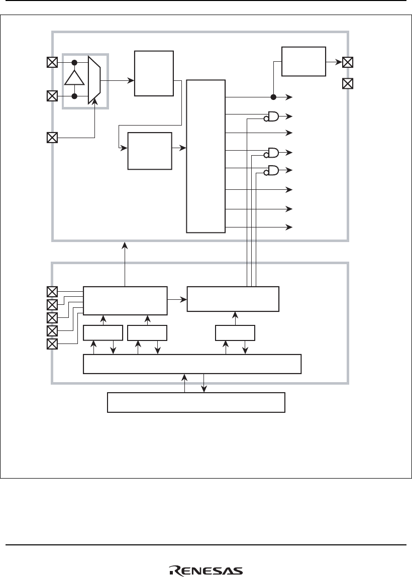
15. Clock Pulse Generator (CPG)
Rev.1.00 Jan. 10, 2008 Page 734 of 1658
REJ09B0261-0100
Oscillator circuit
Control section
Crystal oscillator
circuit
Divider 1
× 1
PLL circuit 1
× 72
× 36
Clock frequency
control circuit
FRQCR0 FRQCR1 MSTPCR1
Clock control circuit
Bus interface
Peripheral bus
PLL circuit 2
× 1 CLKOUT
CLKOUTENB
Divider 2
× 1/2
× 1/4
× 1/6
× 1/8
× 1/12
× 1/16
× 1/18
× 1/24
× 1/32
× 1/36
× 1/48
Bus clock
(Bck)
CPU clock
(Ick)
SHwy clock
(SHck)
GA clock
(GAck)
DU clock
(DUck)
Peripheral clock
(Pck)
DDR clock
(DDRck)
RAM clock
(Uck)
XTAL
EXTAL
MODE 10
MODE 4
MODE 3
MODE 2
MODE 1
MODE 0
Legend:
FRQCR0: Frequency control register 0
FRQCR1: Frequency control register 1
MSTPCR1: Module standby control register 1*
Note: * For details about MSTPCR1, see section 17, Power-Down Mode.
Figure 15.1 Block Diagram of the CPG

15. Clock Pulse Generator (CPG)
Rev.1.00 Jan. 10, 2008 Page 735 of 1658
REJ09B0261-0100
The function of each block in the CPG is as follows.
• PLL circuit 1
PLL circuit 1 multiplies the input clock frequency on the PLL circuit by 36 or 72.
• PLL circuit 2
PLL circuit 2 matches the phases of the bus clock (Bck) and the clock of the CLKOUT pin that
is used in the local bus.
• Crystal oscillator circuit
The crystal oscillator circuit is used when a crystal resonator is connected to the XTAL and
EXTAL pins. The crystal oscillator circuit can be used by the MODE10 pin setting.
For details on input frequency, see section 32, Electrical Characteristics.
• Divider 1
Divider 1 divides the input clock frequency from the crystal oscillator circuit or the EXTAL
pin. The division ratio is set by mode pins MODE3 and MODE4.
• Divider 2
Divider 2 generates the CPU clock (Ick), SuperHyway clock (SHck), GDTA clock (GAck),
DU clock (DUck), peripheral module clock (Pck), DDR clock (DDRck), external bus clock
(Bck), and RAM clock (Uck). The division ratio is selected by mode setting pins MODE0 and
MODE1.

15. Clock Pulse Generator (CPG)
Rev.1.00 Jan. 10, 2008 Page 736 of 1658
REJ09B0261-0100
15.2 Input/Output Pins
Table 15.1 shows the CPG pin configuration.
Table 15.1 CPG Pin Configuration
Pin Name Function I/O Description
MODE0,
MODE1,
MODE2,
MODE3,
and MODE4*1
Mode Pins
0,1,2,3,4
Clock
operating
mode*1
Input Select the clock operating mode
These pins are multiplexed with the following pins.
MODE0: the IRL4 (INTC), FD4 (FLCTL), and PL4 (GPIO) pins
MODE1: the IRL5 (INTC), FD5 (FLCTL), and PL3 (GPIO) pins
MODE2: the IRL6 (INTC), FD6 (FLCTL), and PL2 (GPIO) pins
MODE3: the IRL7 (INTC), FD7 (FLCTL), and PL1 (GPIO) pins
MODE4: the SCIF3_TXD (SCIF channel 3), FCLE (FLCTL), and PN5
(GPIO) pins
MODE10 Mode Pin 10
Clock input
mode*1
Input Selects whether the crystal resonator is used
When MODE10 is set to the low level, the external clock is input from
the EXTAL pin.
When MODE10 is set to the high level, the crystal resonator is
connected directly to the EXTAL and XTAL pins.
MODE10 is multiplexed with the SCIF4_RXD (SCIF channel 4), FD2
(FLCTL), and PN1 (GPIO) pins.
XTAL Output Connected to a crystal resonator
EXTAL Input Used to input an external clock or connected to a crystal resonator.
CLKOUT*2
Clock Pins
Output Used to output a local bus clock
CLKOUTENB Clock Output
Enabled
Output The low level is output when the output clock of the CLKOUT is
unstable.
When the input to the PRESET pin is the low level, the high level is
output regardless of the status of the output clock on the CLKOUT
pin.
Notes: 1. The clock operating mode and the clock input mode depend on the states of the mode
pins on a power-on reset via the PRESET pin.
2. For details on ensuring the AC timing of the CLKOUT pin, see the section about
electrical characteristics. Note the relationship between the input frequency and
multiplication rate of a crystal oscillator circuit.

15. Clock Pulse Generator (CPG)
Rev.1.00 Jan. 10, 2008 Page 737 of 1658
REJ09B0261-0100
15.3 Clock Operating Modes
Table 15.2 shows the relationship between setting of the mode pins (MODE0 to MODE4) and the
clock operating modes.
Table 15.2 Clock Operating Modes and Operations of the Oscillator and PLLs
Setting of Mode Control Pins*1*2 Clock
Operating
Mode MODE4 MODE3 MODE2 MODE1 MODE0 Divider 1 PLL1 PLL2
0 L L L L L × 1 On (× 72) On
1 L L L L H × 1 On (× 72) On
2 L L L H L × 1 On (× 72) On
3 L L L H H × 1 On (× 72) On
16 H L L L L × 1 On (× 36) On
17 H L L L H × 1 On (× 36) On
18 H L L H L × 1 On (× 36) On
19 H L L H H × 1 On (× 36) On
Notes: 1. For the MODE0 to MODE4 pins, setting except the above mode pins (MODE0 to
MODE4) is prohibited.
2. L stands for 'low level', and H stands for 'high level'.

15. Clock Pulse Generator (CPG)
Rev.1.00 Jan. 10, 2008 Page 738 of 1658
REJ09B0261-0100
Table 15.3 Clock Operating Modes and Frequency Multiplication Ratio for Each Clock
(Both MODE12 and MODE11 Are Set to High Level)
Frequency Multiplication Ratio (for Input Clock)
Clock
Operating
Mode
FRQMR1
Initial
Value
CPU
Clock
Ick
RAM
Clock
Uck
SuperHyway
Clock
SHck
GDTA
Clock
GAck
DU Clock
DUck
Peripheral
Clock
Pck
DDR
Clock
DDRck
Bus
Clock
Bck
0 H'1225 2448 × 36 × 18 × 18 × 9 × 9 × 3 × 18 × 6
1 H'122B 244B × 36 × 18 × 18 × 9 × 9 × 3/2 × 18 × 3/2
2 H'1335 3558 × 36 × 12 × 12 × 6 × 6 × 3 × 12 × 6
3 H'133B 355B × 36 × 12 × 12 × 6 × 6 × 3/2 × 12 × 3/2
16 H'1225 2448 × 18 × 9 × 9 × 9/2 × 9/2 × 3/2 × 9 × 3
17 H'122B 244B × 18 × 9 × 9 × 9/2 × 9/2 × 3/4 × 9 × 3/4
18 H'1335 3558 × 18 × 6 × 6 × 3 × 3 × 3/2 × 6 × 3
19 H'133B 355B × 18 × 6 × 6 × 3 × 3 × 3/4 × 6 × 3/4
Table 15.4 Clock Operating Modes and Frequency Multiplication Ratio for Each Clock
(MODE12 or MODE11 Is Set to Low Level)
Frequency Multiplication Ratio (for Input Clock)
Clock
Operating
Mode
FRQMR1
Initial
Value
CPU
Clock
Ick
RAM
Clock
Uck
SuperHyway
Clock
SHck
GDTA
Clock
GAck
DU Clock
DUck
Peripheral
Clock
Pck
DDR
Clock
DDRck
Bus
Clock
Bck
0 H'1225 24F8 × 36 × 18 × 18 × 9 Stopped × 3 × 18 × 6
1 H'122B 24FB × 36 × 18 × 18 × 9 Stopped × 3/2 × 18 × 3/2
2 H'1335 35F8 × 36 × 12 × 12 × 6 Stopped × 3 × 12 × 6
3 H'133B 35FB × 36 × 12 × 12 × 6 Stopped × 3/2 × 12 × 3/2
16 H'1225 24F8 × 18 × 9 × 9 × 9/2 Stopped × 3/2 × 9 × 3
17 H'122B 24FB × 18 × 9 × 9 × 9/2 Stopped × 3/4 × 9 × 3/4
18 H'1335 35F8 × 18 × 6 × 6 × 3 Stopped × 3/2 × 6 × 3
19 H'133B 35FB × 18 × 6 × 6 × 3 Stopped × 3/4 × 6 × 3/4

15. Clock Pulse Generator (CPG)
Rev.1.00 Jan. 10, 2008 Page 739 of 1658
REJ09B0261-0100
15.4 Register Descriptions
Table 15.5 lists the registers. Table 15.6 shows the register states in each processing mode.
Table 15.5 Register Configuration
Register Name Abbreviation R/W P4 Address
Area 7
Address
Access
Size
Sync
Clock
Frequency control register 0 FRQCR0 R/W H'FFC8 0000 H'1FC8 0000 32 Pck
Frequency control register 1 FRQCR1 R/W H'FFC8 0004 H'1FC8 0004 32 Pck
Frequency display register 1 FRQMR1 R H'FFC8 0014 H'1FC8 0014 32 Pck
Sleep control register SLPCR R/W H'FFC8 0020 H'1FC8 0020 32 Pck
PLL control register PLLCR R/W H'FFC8 0024 H'1FC8 0024 32 Pck
Standby control register 0* MSTPCR0 R/W H'FFC8 0030 H'1FC8 0030 32 Pck
Standby control register 1* MSTPCR1 R/W H'FFC8 0034 H'1FC8 0034 32 Pck
Standby display register* MSTPMR R H'FFC8 0044 H'1FC8 0044 32 Pck
Note: * For details on the standby control registers, see section 17, Power-Down Mode.

15. Clock Pulse Generator (CPG)
Rev.1.00 Jan. 10, 2008 Page 740 of 1658
REJ09B0261-0100
Table 15.6 Register State in Each Processing Mode
Register Name Abbreviation
Power-on Reset
by the PRESET
Pin, WDT, or
H-UDI
Manual Reset by
WDT or
Multiple
Exception
Sleep or Deep
Sleep
by Sleep
Instruction
Frequency control register 0 FRQCR0 H'0000 0000 Retained Retained
Frequency control register 1 FRQCR1 H'0000 0000 Retained Retained
Frequency display register 1 FRQMR1 H'1xxx xxxx*2 Retained Retained
Sleep control register SLPCR H'0000 0000 Retained Retained
PLL control register PLLCR H'0000 0000 Retained Retained
Standby control register 0*1 MSTPCR0 H'0000 0000 Retained Retained
Standby control register 1*1 MSTPCR1 H'0000 0000 Retained Retained
Standby display register*1 MSTPMR H'00x0 0000*3 Retained Retained
Notes: 1. For details on the standby control registers, see section 17, Power-Down Mode.
2. The state of this register depends on the settings of mode pins MODE0 to MODE4,
MODE11, and MODE12 obtained on a power-on reset via the PRESET pin. See Table
15.3 or 15.4.
3. The state of this register depends on the setting of mode pins MODE11 and MODE12
obtained on a power-on reset via the PRESET pin.

15. Clock Pulse Generator (CPG)
Rev.1.00 Jan. 10, 2008 Page 741 of 1658
REJ09B0261-0100
15.4.1 Frequency Control Register 0 (FRQCR0)
FRQCR0 is a 32-bit readable and partially writable register that executes a sequence for changing
the frequency of each clock. After the sequence is executed, FRQCR0 is automatically cleared to
0. FRQCR0 can only be accessed in longwords.
To write to FRQCR0, set the code value (H'CF) in the upper byte and use the longword. No other
code values can be written. The code value is always read as 0.
FRQCR0 is initialized by only a power-on reset via the PRESET pin or a WDT overflow.
161718192021222324252627282931 30
0000000000000000
⎯⎯⎯⎯⎯⎯⎯⎯Code value (H'CF)
RRRRRRRRR/WR/WR/WR/WR/WR/WR/W R/W
BIt:
Initial value:
R/W:
01234567891011121315 14
0000000000000000
FRQE
⎯⎯⎯⎯⎯⎯⎯⎯⎯⎯⎯⎯⎯⎯⎯
R/WRRRRRRRRRRRRRRR
BIt:
Initial value:
R/W:
Bit Bit Name
Initial
Value R/W Description
31 to 24 ⎯ All 0 R/W Code value (H'CF)
These bits are always read as 0. The write value
should always be H'CF.
23 to 1 ⎯ All 0 R Reserved
These bits are always read as 0. The write value
should always be 0.
0 FRQE 0 R/W Frequency Change Sequence Enabled
Enables the execution of a sequence that changes the
frequency of each clock according to the value set in
FRQCR1. After executing the sequence, this bit is
automatically cleared to 0.
0: Execution of a sequence that changes the frequency
is disabled.
1: Execution of a sequence that changes the frequency
is enabled.
Note: Some division ratio settings are prohibited. When
a value that is not shown in Tables 15.8 to 15.11
is set in FRQCR1, do not set 1 in FRQE.

15. Clock Pulse Generator (CPG)
Rev.1.00 Jan. 10, 2008 Page 742 of 1658
REJ09B0261-0100
15.4.2 Frequency Control Register 1 (FRQCR1)
FRQCR1 is a 32-bit readable/writable register that can select the division ratio of divider 2 for the
CPU clock (lck), the SuperHyway clock (SHck), the peripheral clock (Pck), the DDR clock
(DDRck), the bus clock (Bck), the GDTA clock (GAck), the DU clock (DUck), and the RAM
clock (Uck). To check the division ratio of divider 2 for each clock, read FRQMR1. FRQCR1 can
only be accessed in longwords.
FRQCR1 only changes the division ratio of a clock to which a value other than H'0 has been
written. Therefore, set a value other than H'0 in the bit corresponding to the clock for which you
want to change the division ratio. Other bits should be set to H'0.
To change the division ratio of each clock to the value set in FRQCR1, you must set 1 in the
FRQE bit in FRQCR0 to execute the sequence that changes the frequency. After the sequence is
executed, this register is automatically cleared to H'0000 0000.
However, when changing the division ratio of the DDR clock (DDRck), switch SDRAM to the
self-refreshing state. For details on how to switch to or release the self-refreshing state, see section
12, DDR2-SDRAM Interface (DBSC2).
FRQCR1 is initialized by only a power-on reset via the PRESET pin or a WDT overflow.
161718192021222324252627282931 30
0000000000000000
BFC0BFC1BFC2BFC3SFC0SFC1SFC2SFC3UFC0UFC1UFC2UFC3IFC0IFC1IFC3 IFC2
R/WR/WR/WR/WR/WR/WR/WR/WR/WR/WR/WR/WR/WR/WR/W R/W
BIt:
Initial value:
R/W:
01234567891011121315 14
0000000000000000
PFC0PFC1PFC2PFC3S3FC0S3FC1S3FC2S3FC3S2FC0S2FC1S2FC2S2FC3MFC0MFC1MFC3 MFC2
R/WR/WR/WR/WR/WR/WR/WR/WR/WR/WR/WR/WR/WR/WR/W R/W
BIt:
Initial value:
R/W:

15. Clock Pulse Generator (CPG)
Rev.1.00 Jan. 10, 2008 Page 743 of 1658
REJ09B0261-0100
Bit Bit Name
Initial
Value R/W Description
31
30
29
28
IFC3
IFC2
IFC1
IFC0
0
0
0
0
R/W
R/W
R/W
R/W
Frequency division ratio of the CPU clock (Ick)
0000: No change
0001: × 1/2
0010: × 1/4
0011: × 1/6
Others: Setting prohibited
27
26
25
24
UFC3
UFC2
UFC1
UFC0
0
0
0
0
R/W
R/W
R/W
R/W
Frequency division ratio of the RAM clock (Uck)
0000: No change
0010: × 1/4
0011: × 1/6
Others: Setting prohibited
23
22
21
20
SFC3
SFC2
SFC1
SFC0
0
0
0
0
R/W
R/W
R/W
R/W
Frequency division ratio of the SuperHyway clock
(SHck)
0000: No change
0010: × 1/4
0011: × 1/6
Others: Setting prohibited
19
18
17
16
BFC3
BFC2
BFC1
BFC0
0
0
0
0
R/W
R/W
R/W
R/W
Frequency division ratio of the bus clock (Bck)
0000: No change
0101: × 1/12
0110: × 1/16
0111: × 1/18
1000: × 1/24
1001: × 1/32
1010: × 1/36
1011: × 1/48
Others: Setting prohibited
15
14
13
12
MFC3
MFC2
MFC1
MFC0
0
0
0
0
R/W
R/W
R/W
R/W
Frequency division ratio of the DDR clock (DDRck)
0000: No change
0010: × 1/4
0011: × 1/6
Others: Setting prohibited

15. Clock Pulse Generator (CPG)
Rev.1.00 Jan. 10, 2008 Page 744 of 1658
REJ09B0261-0100
Bit Bit Name
Initial
Value R/W Description
11
10
9
8
S2FC3
S2FC2
S2FC1
S2FC0
0
0
0
0
R/W
R/W
R/W
R/W
Frequency division ratio of the GDTA clock (GAck)
0000: No change
0100: × 1/8
0101: × 1/12
Others: Setting prohibited
7
6
5
4
S3FC3
S3FC2
S3FC1
S3FC0
0
0
0
0
R/W
R/W
R/W
R/W
Frequency division ratio of the DU clock (DUck)
0000: No change
0100: × 1/8
0101: × 1/12
0110: × 1/16
0111: × 1/18
1000: × 1/24
1001: × 1/32
1010: × 1/36
1011: × 1/48
Others: Setting prohibited
3
2
1
0
PFC3
PFC2
PFC1
PFC0
0
0
0
0
R/W
R/W
R/W
R/W
Frequency division ratio of the peripheral clock (Pck)
0000: No change
0111: × 1/18
1000: × 1/24
1001: × 1/32
1010: × 1/36
1011: × 1/48
Others: Setting prohibited

15. Clock Pulse Generator (CPG)
Rev.1.00 Jan. 10, 2008 Page 745 of 1658
REJ09B0261-0100
15.4.3 Frequency Display Register 1 (FRQMR1)
FRQMR1 is a 32-bit readable register that reads the division ratio of divider 2 for the CPU clock
(lck), the SuperHyway clock (SHck), the peripheral clock (Pck), the DDR clock (DDRck),the bus
clock (Bck), the GDTA clock (GAck), the DU clock (DUck), and the RAM clock (Uck).
FRQMR1 can only be accessed in longwords.
This register is initialized by only a power-on reset via the PRESET pin or a WDT overflow.
161718192021222324252627282931 30
1xxxx100x1001000
BFST0BFST1BFST2BFST3SFST0SFST1SFST2SFST3UFST0UFST1UFST2UFST3IFST0IFST1IFST3 IFST2
RRRRRRRRRRRRRRRR
BIt:
Initial value:
R/W:
01234567891011121315 14
xx01xx1xx010x100
PFST0PFST1PFST2PFST3
S3FST0S3FST1S3FST2S3FST3S2FST0S2FST1S2FST2S2FST3
MFST0MFST1MFST3 MFST2
RRRRRRRRRRRRRRRR
BIt:
Initial value:
R/W:
Note: The initial value (x: a bit whose value is undefined) depends on the settings of mode pins
MODE0 to MODE4, MODE11, and MODE12 on a power-on reset via the PRESET pin.
See Table 15.3 or 15.4.
Bit Bit Name
Initial
Value R/W Description
31
30
29
28
IFST3
IFST2
IFST1
IFST0
0
0
0
1
R
R
R
R
Frequency division ratio of the CPU clock (Ick)
0001: × 1/2
0010: × 1/4
0011: × 1/6
27
26
25
24
UFST3
UFST2
UFST1
UFST0
0
0
1
x
R
R
R
R
Frequency division ratio of the RAM clock (Uck)
0010: × 1/4
0011: × 1/6
23
22
21
20
SFST3
SFST2
SFST1
SFST0
0
0
1
x
R
R
R
R
Frequency division ratio of the SuperHyway clock
(SHck)
0010: × 1/4
0011: × 1/6

15. Clock Pulse Generator (CPG)
Rev.1.00 Jan. 10, 2008 Page 746 of 1658
REJ09B0261-0100
Bit Bit Name
Initial
Value R/W Description
19
18
17
16
BFST3
BFST2
BFST1
BFST0
x
x
x
1
R
R
R
R
Frequency division ratio of the bus clock (Bck)
0101: × 1/12
0110: × 1/16
0111: × 1/18
1000: × 1/24
1001: × 1/32
1010: × 1/36
1011: × 1/48
15
14
13
12
MFST3
MFST2
MFST1
MFST0
0
0
1
x
R
R
R
R
Frequency division ratio of the DDR clock (DDRck)
0010: ×1/4
0011: ×1/6
11
10
9
8
S2FST3
S2FST2
S2FST1
S2FST0
0
1
0
x
R
R
R
R
Frequency division ratio of the GDTA clock (GAck)
0100: × 1/8
0101: × 1/12
1111: Stop the clock supply.
7
6
5
4
S3FST3
S3FST3
S3FST3
S3FST3
x
1
x
x
R
R
R
R
Frequency division ratio of the DU clock (DUck)
0100: × 1/8
0101: × 1/12
0110: × 1/16
0111: × 1/18
1000: × 1/24
1001: × 1/32
1010: × 1/36
1011: × 1/48
1111: Stop the clock supply
3
2
1
0
PFST3
PFST2
PFST1
PFST0
1
0
x
x
R
R
R
R
Frequency division ratio of the peripheral clock (Pck)
0111: × 1/18
1000: × 1/24
1001: × 1/32
1010: × 1/36
1011: × 1/48

15. Clock Pulse Generator (CPG)
Rev.1.00 Jan. 10, 2008 Page 747 of 1658
REJ09B0261-0100
15.4.4 PLL Control Register (PLLCR)
PLLCR is a 32-bit readable/writable register that controls the clock output on the CLKOUT pin.
This register can only be accessed in longwords.
161718192021222324252627282931 30
0000000000000000
⎯⎯⎯⎯⎯⎯⎯⎯⎯⎯⎯⎯⎯⎯⎯⎯
R/WR/WR/WR/WR/WR/WR/WR/WRRRRRRRR
BIt:
Initial value:
R/W:
01234567891011121315 14
0000000000000000
⎯
CKOFF
⎯⎯⎯⎯⎯⎯⎯⎯⎯⎯⎯⎯⎯⎯
RR/WRRRRRRRRRRRRRR
BIt:
Initial value:
R/W:
Bit Bit Name
Initial
Value R/W Description
31 to 24 ⎯ 0 R Reserved
These bits are always read as 0. The write value
should always be 0.
23 to 16 ⎯ All 0 R/W Reserved
These bits are always read as 0. The write value
should always be 0. If a value other than 0 is written,
the operation is not guaranteed.
15 to 2 ⎯ All 0 R Reserved
These bits are always read as 0. The write value
should always be 0.
1 CKOFF 0 R/W CLKOUT Output Enabled
Stops clock output on the CLKOUT pin
0: Clock is output on the CLKOUT pin
1: The CLKOUT pin is placed in the high impedance
state
0 ⎯ 0 R Reserved
This bit is always read as 0. The write value should
always be 0.

15. Clock Pulse Generator (CPG)
Rev.1.00 Jan. 10, 2008 Page 748 of 1658
REJ09B0261-0100
15.5 Calculating the Frequency
Table 15.7 shows the relationship between the division ratio of divider 2 described for frequency
control register FRQCR1 and frequency display register FRQMR1, and the EXTAL input.
Table 15.7 Relationship Between the Division Ratio of Divider 2 and the Frequency
Frequency (for an input clock)
Division ratio of
divider 2 Clock operating mode 0 to 3 Clock operating mode 16 to 19
× 1/2 × 36 × 18
× 1/4 × 18 × 9
× 1/6 × 12 × 6
× 1/8 × 9 × 9/2
× 1/12 × 6 × 3
× 1/16 × 9/2 × 9/4
× 1/18 × 4 × 2
× 1/24 × 3 × 3/2
× 1/32 × 9/4 × 9/8
× 1/36 × 2 × 1
× 1/48 × 3/2 × 3/4

15. Clock Pulse Generator (CPG)
Rev.1.00 Jan. 10, 2008 Page 749 of 1658
REJ09B0261-0100
15.6 How to Change the Frequency
To change the frequency of the internal clock and the local bus clock (CLKOUT) with software,
set frequency control registers FRQCR0 and FRQCR1 according to the following procedure.
Tables 15.8 to 15.11 list the selectable combinations of frequencies.
15.6.1 Changing the Frequency of Clocks Other than the Bus Clock
When changing the frequency of a clock except the bus clock, disable counting-up by the WDT.
The following describes the procedure for changing the frequency.
1. In FRQCR1, set a value (other than H'0) in the bit corresponding to the clock for which you
want to change the division ratio.*
2. Set H'CF000001 in FRQCR0 to enable execution of the sequence that changes the frequency.
The sequence that changes the frequency starts.
3. When H'00000000 is read from FRQCR0, the sequence that changes the frequency has
finished. The internal clock has been changed to the clock with the specified division ratio.
Note: * When setting a value except H'0 in the MFC3 to MFC0 bits in FRQCR1 to change the
DDR clock frequency, switch SDRAM to the self-refreshing state before executing
step (2) above. For details on how to switch to or release the self-refreshing state, see
section 12, DDR2-SDRAM Interface (DBSC2).
15.6.2 Changing the Bus Clock Frequency
When changing the bus clock frequency, start counting-up by the WDT after the oscillation of
PLL circuit 2 is stable. When a WDT overflow occurs during counting, this LSI resumes
operation.
Figures 15.2 and 15.3 show the timing of the CLKOUT and CLKOUTENB pins when the bus
clock frequency is changed.
The following describes the procedure for changing the frequency.
1. Write 0 to the TME bit in WDTCSR to stop the WDT.
2. In WDTBST, after the oscillation of PLL circuit 2 is stable, set the time that can elapse before
the LSI resumes operation. Writing H'55000001 sets the minimum value. Writing H'55000000
sets the maximum value.
3. In FRQCR1, set a value (except H'0) in the bit corresponding to the clock for which you want
to change the division ratio.*
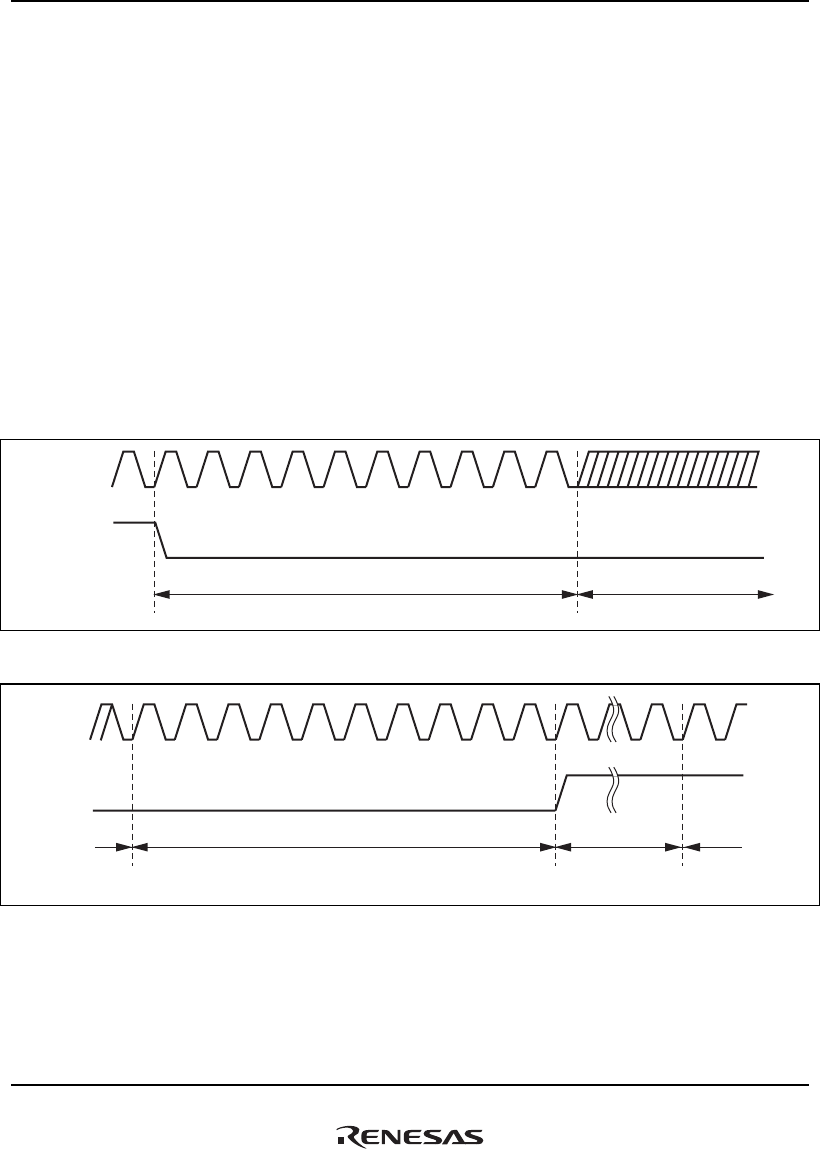
15. Clock Pulse Generator (CPG)
Rev.1.00 Jan. 10, 2008 Page 750 of 1658
REJ09B0261-0100
4. Set H'CF000001 in FRQCR0 to enable execution of the sequence that changes the frequency.
The sequence that changes the frequency starts.
5. The CLKOUTENB pin output changes to low level. After ten cycles of the peripheral clock
(Pck), an unstable clock is output to the CLKOUT pin.
6. When the oscillation of PLL circuit 2 is stable, wait for ten cycles of the peripheral clock
(Pck). Then output a high level signal to the CLKOUTENB pin.
7. When the WDT starts counting up and the value of WDTBCNT is equal to the value of
WDTBST, the LSI resumes operation.
8. When H'00000000 is read from FRQCR0, the sequence that changes the frequency has
finished. The internal clock has been changed to the clock with the specified division ratio.
Note: * When setting a value except H'0 in the MFC3 to MFC0 bits in FRQCR1 to change the
DDR clock frequency, switch SDRAM to the self-refreshing state before executing
step (2) above. For details on how to switch to or release the self-refreshing state, see
section 12, DDR2-SDRAM Interface (DBSC2).
CLKOUT
output
Ten peripheral clock cycles PLL circuit 2 oscillation starts
CLKOUTENB
output
Figure 15.2 Beginning of the Change of the Bus Clock Frequency
CLKOUT
output
Ten peripheral clock cycles Operation restarts
PLL circuit 2 stabilized oscillation Counting-up by the WDT
CLKOUTENB
output
Figure 15.3 End of the Change of the Bus Clock Frequency

15. Clock Pulse Generator (CPG)
Rev.1.00 Jan. 10, 2008 Page 751 of 1658
REJ09B0261-0100
Table 15.8 Selectable Combinations of Clock Frequency (CPU Clock: × 1/2, DDR Clock: ×
1/4)
Division ratio of divider 2
FRQMR1
read value
CPU
clock
Ick
RAM
clock
Uck
SuperHyway
clock
SHck
GDTA
clock
GAck
DU
clock
DUck
Peripheral
clock
Pck
DDR
clock
DDRck
Bus
clock
Bck
H'1225 2448 × 1/2 × 1/4 × 1/4 × 1/8 × 1/8 × 1/24 × 1/4 × 1/12
H'1225 2458 × 1/2 × 1/4 × 1/4 × 1/8 × 1/12 × 1/24 × 1/4 × 1/12
H'1225 2488 × 1/2 × 1/4 × 1/4 × 1/8 × 1/24 × 1/24 × 1/4 × 1/12
H'1225 244B × 1/2 × 1/4 × 1/4 × 1/8 × 1/8 × 1/48 × 1/4 × 1/12
H'1225 245B × 1/2 × 1/4 × 1/4 × 1/8 × 1/12 × 1/48 × 1/4 × 1/12
H'1225 246B × 1/2 × 1/4 × 1/4 × 1/8 × 1/16 × 1/48 × 1/4 × 1/12
H'1225 248B × 1/2 × 1/4 × 1/4 × 1/8 × 1/24 × 1/48 × 1/4 × 1/12
H'1225 24BB × 1/2 × 1/4 × 1/4 × 1/8 × 1/48 × 1/48 × 1/4 × 1/12
H'1226 244A × 1/2 × 1/4 × 1/4 × 1/8 × 1/8 × 1/36 × 1/4 × 1/16
H'1226 246A × 1/2 × 1/4 × 1/4 × 1/8 × 1/16 × 1/36 × 1/4 × 1/16
H'1226 24AA × 1/2 × 1/4 × 1/4 × 1/8 × 1/36 × 1/36 × 1/4 × 1/16
H'1226 244B × 1/2 × 1/4 × 1/4 × 1/8 × 1/8 × 1/48 × 1/4 × 1/16
H'1226 245B × 1/2 × 1/4 × 1/4 × 1/8 × 1/12 × 1/48 × 1/4 × 1/16
H'1226 246B × 1/2 × 1/4 × 1/4 × 1/8 × 1/16 × 1/48 × 1/4 × 1/16
H'1226 248B × 1/2 × 1/4 × 1/4 × 1/8 × 1/24 × 1/48 × 1/4 × 1/16
H'1226 24BB × 1/2 × 1/4 × 1/4 × 1/8 × 1/48 × 1/48 × 1/4 × 1/16
H'1228 2448 × 1/2 × 1/4 × 1/4 × 1/8 × 1/8 × 1/24 × 1/4 × 1/24
H'1228 2458 × 1/2 × 1/4 × 1/4 × 1/8 × 1/12 × 1/24 × 1/4 × 1/24
H'1228 2488 × 1/2 × 1/4 × 1/4 × 1/8 × 1/24 × 1/24 × 1/4 × 1/24
H'1228 244B × 1/2 × 1/4 × 1/4 × 1/8 × 1/8 × 1/48 × 1/4 × 1/24
H'1228 245B × 1/2 × 1/4 × 1/4 × 1/8 × 1/12 × 1/48 × 1/4 × 1/24
H'1228 246B × 1/2 × 1/4 × 1/4 × 1/8 × 1/16 × 1/48 × 1/4 × 1/24
H'1228 248B × 1/2 × 1/4 × 1/4 × 1/8 × 1/24 × 1/48 × 1/4 × 1/24
H'1228 24BB × 1/2 × 1/4 × 1/4 × 1/8 × 1/48 × 1/48 × 1/4 × 1/24
H'122A 244A × 1/2 × 1/4 × 1/4 × 1/8 × 1/8 × 1/36 × 1/4 × 1/36
H'122A 246A × 1/2 × 1/4 × 1/4 × 1/8 × 1/16 × 1/36 × 1/4 × 1/36
H'122A 24AA × 1/2 × 1/4 × 1/4 × 1/8 × 1/36 × 1/36 × 1/4 × 1/36

15. Clock Pulse Generator (CPG)
Rev.1.00 Jan. 10, 2008 Page 752 of 1658
REJ09B0261-0100
Division ratio of divider 2
FRQMR1
read value
CPU
clock
Ick
RAM
clock
Uck
SuperHyway
clock
SHck
GDTA
clock
GAck
DU
clock
DUck
Peripheral
clock
Pck
DDR
clock
DDRck
Bus
clock
Bck
H'122B 244B × 1/2 × 1/4 × 1/4 × 1/8 × 1/8 × 1/48 × 1/4 × 1/48
H'122B 245B × 1/2 × 1/4 × 1/4 × 1/8 × 1/12 × 1/48 × 1/4 × 1/48
H'122B 246B × 1/2 × 1/4 × 1/4 × 1/8 × 1/16 × 1/48 × 1/4 × 1/48
H'122B 248B × 1/2 × 1/4 × 1/4 × 1/8 × 1/24 × 1/48 × 1/4 × 1/48
H'122B 24BB × 1/2 × 1/4 × 1/4 × 1/8 × 1/48 × 1/48 × 1/4 × 1/48
Table 15.9 Selectable Combinations of Clock Frequency (CPU Clock: × 1/4, DDR Clock: ×
1/4)
Division ratio of divider 2
FRQMR1 read
value
CPU
clock
Ick
RAM
clock
Uck
SuperHyway
clock
SHck
GDTA
clock
GAck
DU
clock
DUck
Peripheral
clock
Pck
DDR
clock
DDRck
Bus
clock
Bck
H'2225 2448 × 1/4 × 1/4 × 1/4 × 1/8 × 1/8 × 1/24 × 1/4 × 1/12
H'2225 2458 × 1/4 × 1/4 × 1/4 × 1/8 × 1/12 × 1/24 × 1/4 × 1/12
H'2225 2488 × 1/4 × 1/4 × 1/4 × 1/8 × 1/24 × 1/24 × 1/4 × 1/12
H'2225 244B × 1/4 × 1/4 × 1/4 × 1/8 × 1/8 × 1/48 × 1/4 × 1/12
H'2225 245B × 1/4 × 1/4 × 1/4 × 1/8 × 1/12 × 1/48 × 1/4 × 1/12
H'2225 246B × 1/4 × 1/4 × 1/4 × 1/8 × 1/16 × 1/48 × 1/4 × 1/12
H'2225 248B × 1/4 × 1/4 × 1/4 × 1/8 × 1/24 × 1/48 × 1/4 × 1/12
H'2225 24BB × 1/4 × 1/4 × 1/4 × 1/8 × 1/48 × 1/48 × 1/4 × 1/12
H'2226 244A × 1/4 × 1/4 × 1/4 × 1/8 × 1/8 × 1/36 × 1/4 × 1/16
H'2226 246A × 1/4 × 1/4 × 1/4 × 1/8 × 1/16 × 1/36 × 1/4 × 1/16
H'2226 24AA × 1/4 × 1/4 × 1/4 × 1/8 × 1/36 × 1/36 × 1/4 × 1/16
H'2226 244B × 1/4 × 1/4 × 1/4 × 1/8 × 1/8 × 1/48 × 1/4 × 1/16
H'2226 245B × 1/4 × 1/4 × 1/4 × 1/8 × 1/12 × 1/48 × 1/4 × 1/16
H'2226 246B × 1/4 × 1/4 × 1/4 × 1/8 × 1/16 × 1/48 × 1/4 × 1/16
H'2226 248B × 1/4 × 1/4 × 1/4 × 1/8 × 1/24 × 1/48 × 1/4 × 1/16
H'2226 24BB × 1/4 × 1/4 × 1/4 × 1/8 × 1/48 × 1/48 × 1/4 × 1/16
H'2228 2448 × 1/4 × 1/4 × 1/4 × 1/8 × 1/8 × 1/24 × 1/4 × 1/24

15. Clock Pulse Generator (CPG)
Rev.1.00 Jan. 10, 2008 Page 753 of 1658
REJ09B0261-0100
Division ratio of divider 2
FRQMR1 read
value
CPU
clock
Ick
RAM
clock
Uck
SuperHyway
clock
SHck
GDTA
clock
GAck
DU
clock
DUck
Peripheral
clock
Pck
DDR
clock
DDRck
Bus
clock
Bck
H'2228 2458 × 1/4 × 1/4 × 1/4 × 1/8 × 1/12 × 1/24 × 1/4 × 1/24
H'2228 2488 × 1/4 × 1/4 × 1/4 × 1/8 × 1/24 × 1/24 × 1/4 × 1/24
H'2228 244B × 1/4 × 1/4 × 1/4 × 1/8 × 1/8 × 1/48 × 1/4 × 1/24
H'2228 245B × 1/4 × 1/4 × 1/4 × 1/8 × 1/12 × 1/48 × 1/4 × 1/24
H'2228 246B × 1/4 × 1/4 × 1/4 × 1/8 × 1/16 × 1/48 × 1/4 × 1/24
H'2228 248B × 1/4 × 1/4 × 1/4 × 1/8 × 1/24 × 1/48 × 1/4 × 1/24
H'2228 24BB × 1/4 × 1/4 ×1/4 × 1/8 × 1/48 × 1/48 × 1/4 × 1/24
H'222A 244A × 1/4 × 1/4 × 1/4 × 1/8 × 1/8 × 1/36 × 1/4 × 1/36
H'222A 246A × 1/4 × 1/4 × 1/4 × 1/8 × 1/16 × 1/36 × 1/4 × 1/36
H'222A 24AA × 1/4 × 1/4 × 1/4 × 1/8 × 1/36 × 1/36 × 1/4 × 1/36
H'222B 244B × 1/4 × 1/4 × 1/4 × 1/8 × 1/8 × 1/48 × 1/4 × 1/48
H'222B 245B × 1/4 × 1/4 × 1/4 × 1/8 × 1/12 × 1/48 × 1/4 × 1/48
H'222B 246B × 1/4 × 1/4 × 1/4 × 1/8 × 1/16 × 1/48 × 1/4 × 1/48
H'222B 248B × 1/4 × 1/4 × 1/4 × 1/8 × 1/24 × 1/48 × 1/4 × 1/48
H'222B 24BB × 1/4 × 1/4 × 1/4 × 1/8 × 1/48 × 1/48 × 1/4 × 1/48

15. Clock Pulse Generator (CPG)
Rev.1.00 Jan. 10, 2008 Page 754 of 1658
REJ09B0261-0100
Table 15.10 Selectable Combinations of Clock Frequency (CPU Clock: × 1/2, DDR Clock: ×
1/6)
Division ratio of divider 2
FRQMR1 read
value
CPU
clock
Ick
RAM
clock
Uck
SuperHyway
clock
SHck
GDTA
clock
GAck
DU
clock
DUck
Peripheral
clock
Pck
DDR
clock
DDRck
Bus
clock
Bck
H'1335 3558 × 1/2 × 1/6 × 1/6 × 1/12 × 1/12 × 1/24 × 1/6 × 1/12
H'1335 3588 × 1/2 × 1/6 × 1/6 × 1/12 × 1/24 × 1/24 × 1/6 × 1/12
H'1335 355A × 1/2 × 1/6 × 1/6 × 1/12 × 1/12 × 1/36 × 1/6 × 1/12
H'1335 357A × 1/2 × 1/6 × 1/6 × 1/12 × 1/18 × 1/36 × 1/6 × 1/12
H'1335 35AA × 1/2 × 1/6 × 1/6 × 1/12 × 1/36 × 1/36 × 1/6 × 1/12
H'1335 355B × 1/2 × 1/6 × 1/6 × 1/12 × 1/12 × 1/48 × 1/6 × 1/12
H'1335 358B × 1/2 × 1/6 × 1/6 × 1/12 × 1/24 × 1/48 × 1/6 × 1/12
H'1335 35BB × 1/2 × 1/6 × 1/6 × 1/12 × 1/48 × 1/48 × 1/6 × 1/12
H'1337 355A × 1/2 × 1/6 × 1/6 × 1/12 × 1/12 × 1/36 × 1/6 × 1/18
H'1337 357A × 1/2 × 1/6 × 1/6 × 1/12 × 1/18 × 1/36 × 1/6 × 1/18
H'1337 35AA × 1/2 × 1/6 × 1/6 × 1/12 × 1/36 × 1/36 × 1/6 × 1/18
H'1338 3558 × 1/2 × 1/6 × 1/6 × 1/12 × 1/12 × 1/24 × 1/6 × 1/24
H'1338 3588 × 1/2 × 1/6 × 1/6 × 1/12 × 1/24 × 1/24 × 1/6 × 1/24
H'1338 355B × 1/2 × 1/6 × 1/6 × 1/12 × 1/12 × 1/48 × 1/6 × 1/24
H'1338 358B × 1/2 × 1/6 × 1/6 × 1/12 × 1/24 × 1/48 × 1/6 × 1/24
H'1338 35BB × 1/2 × 1/6 × 1/6 × 1/12 × 1/48 × 1/48 × 1/6 × 1/24
H'133A 355A × 1/2 × 1/6 × 1/6 × 1/12 × 1/12 × 1/36 × 1/6 × 1/36
H'133A 357A × 1/2 × 1/6 × 1/6 × 1/12 × 1/18 × 1/36 × 1/6 × 1/36
H'133A 35AA × 1/2 × 1/6 × 1/6 × 1/12 × 1/36 × 1/36 × 1/6 × 1/36
H'133B 355B × 1/2 × 1/6 × 1/6 × 1/12 × 1/12 × 1/48 × 1/6 × 1/48
H'133B 358B × 1/2 × 1/6 × 1/6 × 1/12 × 1/24 × 1/48 × 1/6 × 1/48
H'133B 35BB × 1/2 × 1/6 × 1/6 × 1/12 × 1/48 × 1/48 × 1/6 × 1/48

15. Clock Pulse Generator (CPG)
Rev.1.00 Jan. 10, 2008 Page 755 of 1658
REJ09B0261-0100
Table 15.11 Selectable Combinations of Clock Frequency (CPU Clock: × 1/6, DDR Clock: ×
1/6)
Division ratio of divider 2
FRQMR1
read value
CPU
clock
Ick
RAM
clock
Uck
SuperHyway
clock
SHck
GDTA
clock
GAck
DU
clock
DUck
Peripheral
clock
Pck
DDR
clock
DDRck
Bus
clock
Bck
H'3335 3558 × 1/6 × 1/6 × 1/6 × 1/12 × 1/12 × 1/24 × 1/6 × 1/12
H'3335 3588 × 1/6 × 1/6 × 1/6 × 1/12 × 1/24 × 1/24 × 1/6 × 1/12
H'3335 355A × 1/6 × 1/6 × 1/6 × 1/12 × 1/12 × 1/36 × 1/6 × 1/12
H'3335 357A × 1/6 × 1/6 × 1/6 × 1/12 × 1/18 × 1/36 × 1/6 × 1/12
H'3335 35AA × 1/6 × 1/6 × 1/6 × 1/12 × 1/36 × 1/36 × 1/6 × 1/12
H'3335 355B × 1/6 × 1/6 × 1/6 × 1/12 × 1/12 × 1/48 × 1/6 × 1/12
H'3335 358B × 1/6 × 1/6 × 1/6 × 1/12 × 1/24 × 1/48 × 1/6 × 1/12
H'3335 35BB × 1/6 × 1/6 × 1/6 × 1/12 × 1/48 × 1/48 × 1/6 × 1/12
H'3337 355A × 1/6 × 1/6 × 1/6 × 1/12 × 1/12 × 1/36 × 1/6 × 1/18
H'3337 357A × 1/6 × 1/6 × 1/6 × 1/12 × 1/18 × 1/36 × 1/6 × 1/18
H'3337 35AA × 1/6 × 1/6 × 1/6 × 1/12 × 1/36 × 1/36 × 1/6 × 1/18
H'3338 3558 × 1/6 × 1/6 × 1/6 × 1/12 × 1/12 × 1/24 × 1/6 × 1/24
H'3338 3588 × 1/6 × 1/6 × 1/6 × 1/12 × 1/24 × 1/24 × 1/6 × 1/24
H'3338 355B × 1/6 × 1/6 × 1/6 × 1/12 × 1/12 × 1/48 × 1/6 × 1/24
H'3338 358B × 1/6 × 1/6 × 1/6 × 1/12 × 1/24 × 1/48 × 1/6 × 1/24
H'3338 35BB × 1/6 × 1/6 × 1/6 × 1/12 × 1/48 × 1/48 × 1/6 × 1/24
H'333A 355A × 1/6 × 1/6 × 1/6 × 1/12 × 1/12 × 1/36 × 1/6 × 1/36
H'333A 357A × 1/6 × 1/6 × 1/6 × 1/12 × 1/18 × 1/36 × 1/6 × 1/36
H'333A 35AA × 1/6 × 1/6 × 1/6 × 1/12 × 1/36 × 1/36 × 1/6 × 1/36
H'333B 355B × 1/6 × 1/6 × 1/6 × 1/12 × 1/12 × 1/48 × 1/6 × 1/48
H'333B 358B × 1/6 × 1/6 × 1/6 × 1/12 × 1/24 × 1/48 × 1/6 × 1/48
H'333B 35BB × 1/6 × 1/6 × 1/6 × 1/12 × 1/48 × 1/48 × 1/6 × 1/48
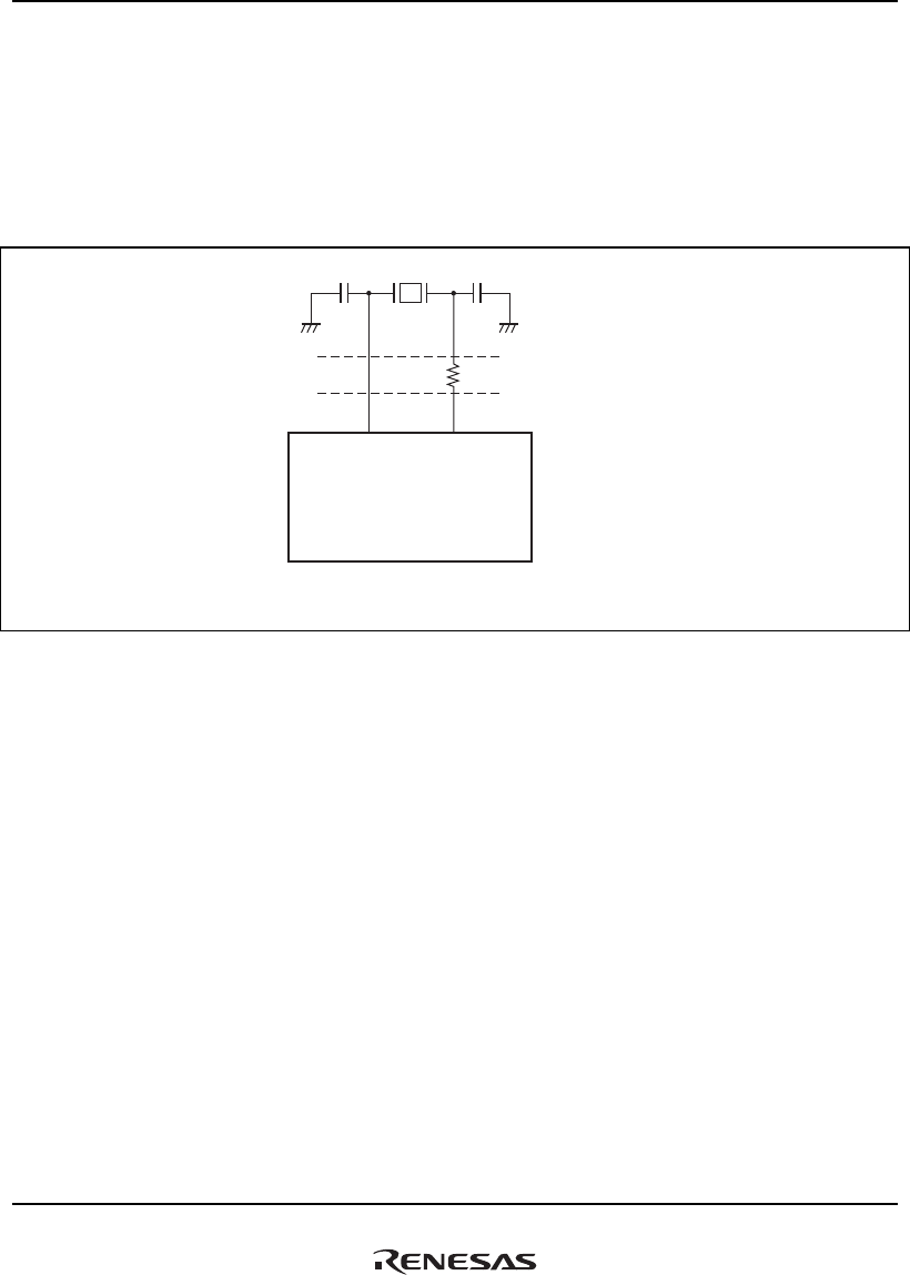
15. Clock Pulse Generator (CPG)
Rev.1.00 Jan. 10, 2008 Page 756 of 1658
REJ09B0261-0100
15.7 Notes on Designing Board
1. Note on Using a Crystal Resonator
Place the crystal resonator and capacitors close to the EXTAL and XTAL pins as much as
possible. No other signal lines should cross the signal line of these pins. Induction may prevent
correct oscillation.
EXTAL XTAL
SH7785
CL1 CL2
R
Crossing of signal lines
is prohibited
Recommended values
CL1 = CL2 = 0 to 33 pF
R = 0 Ω
Note: The values of CL1, CL2, and the dumping resistance should be determined through
evaluation and consultation with the manufacturer of the crystal resonator to be used.
Figure 15.4 Note on Using a Crystal Resonator
2. Note on Inputting the External Clock from the EXTAL Pin
Do not connect anything to the XTAL pin.
3. Note on Using a PLL Oscillator Circuit
Place VDDQ-PLL1, VDDQ-PLL2, VSSQ-PLL1, and VSSQ-PLL2 away from other VDDs
and VSSs on the power supply of the board. Insert resistors RCB, and bypass capacitors, CPB
and CB, as noise filters near the pins.
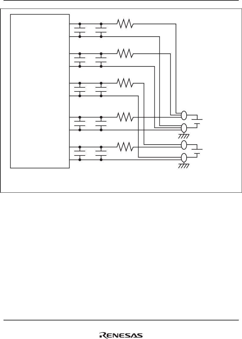
15. Clock Pulse Generator (CPG)
Rev.1.00 Jan. 10, 2008 Page 757 of 1658
REJ09B0261-0100
CB1 RCB1
CPB1
CB2 RCB2
CPB2
CB3 RCB3
CPB3
CB4 RCB4
CPB4
CB5 RCB5
CPB5
Power supply 1
Power supply 2
SH7785
VDD-PLL1
VSS-PLL1
VDDA-PLL1
VSSA-PLL1
VDDQ-PLL1
VSSQ-PLL1
VDD-PLL2
VSS-PLL2
VDDQ-PLL2
VSSQ-PLL2
Recommended values: RCB1 = RCB2 = RCB3 = RCB4 = RCB5 = 10 Ω
CPB1 = CPB2 = CPB3 = CPB4 = CPB5 = 10 μF (Tantalum capacitor)
CB1 = CB2 = CB3 = CB4 = CB5 = 0.1 μF
Figure 15.5 Note on Using a PLL Oscillator Circuit

15. Clock Pulse Generator (CPG)
Rev.1.00 Jan. 10, 2008 Page 758 of 1658
REJ09B0261-0100

16. Watchdog Timer and Reset (WDT)
Rev.1.00 Jan. 10, 2008 Page 759 of 1658
REJ09B0261-0100
Section 16 Watchdog Timer and Reset (WDT)
The watchdog timer and reset module (WDT) comprises a reset control unit and a watchdog timer
control unit, and controls the power-on reset sequence and internal reset of the LSI.
The WDT is a single-channel timer that can be used either as a watchdog timer or interval timer.
16.1 Features
• The watchdog timer unit monitors for system runaway using a timer counting at regular time
intervals.
• Two operating modes:
⎯ In watchdog timer mode, internal reset of the chip is initiated on counter overflow and on-
chip modules are reset.
⎯ In interval timer mode, an interrupt is generated on counter overflow.
• Selectable between power-on reset and manual reset. When manual reset is selected, a manual
reset signal is output from the MRESETOUT pin.
• In order to prevent accidental writing to the WDT-related registers, writing to them is only
possible when a certain code is set in the uppermost eight bits in the data for writing.
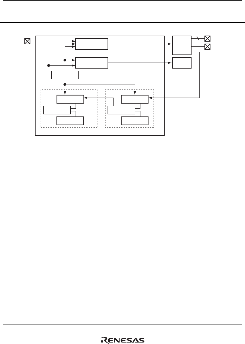
16. Watchdog Timer and Reset (WDT)
Rev.1.00 Jan. 10, 2008 Page 760 of 1658
REJ09B0261-0100
Figure 16.1 is a block diagram of the WDT.
PRESET
MRESETOU
T
Watchdog Timer and Reset module (WDT) STATUS[1:0]
Internal reset request
2
WDTCNT
WDTCSR
WDTST
Count-up signal
Comparator
Reset control
circuit CPG
Interrupt request
Interrupt
control circuit INTC
Peripheral clock
(Pck)
Legend:
WDTCNT: Watchdog timer counter
WDTST: Watchdog timer stop time register
WDTBCNT: Watchdog timer base counter
WDTBST: Watchdog timer base stop time register
WDTCSR: Watchdog timer control/status register
WDTBCNT
WDTBST
Comparator
Figure 16.1 Block Diagram of WDT

16. Watchdog Timer and Reset (WDT)
Rev.1.00 Jan. 10, 2008 Page 761 of 1658
REJ09B0261-0100
16.2 Input/Output Pins
Table 16.1 shows the pin configuration of the WDT module.
Table 16.1 Pin Configuration
Pin name Function I/O Description
PRESET Power-on reset input Input A low level input to this pin places the LSI in
the power-on reset state.
MRESETOUT Manual reset output Output Low level is output during manual reset
execution.
This pin is multiplexed with the IRQOUT
(INTC) pin.
Indicate the LSI's operating status
STATUS1
High
High
Low
STATUS0
High
Low
Low
Operating Status
Reset
Sleep mode
Normal operation
STATUS[1:0] Status output Output
The STATUS1 pin is multiplexed with the
DRAK1 (DMAC) and PK6 (GPIO) pins.
The STATUS0 pin is multiplexed with the
DRAK0 (DMAC) and PK7 (GPIO) pins.

16. Watchdog Timer and Reset (WDT)
Rev.1.00 Jan. 10, 2008 Page 762 of 1658
REJ09B0261-0100
16.3 Register Descriptions
Table 16.2 shows the registers of the WDT module. Table 16.3 shows the register states in each
operating mode.
Table 16.2 Register Configuration
Register Name Abbreviation R/W P4 Address
Area 7
Address
Access
Size
Sync
Clock
Watchdog timer stop time register WDTST R/W H'FFCC 0000 H'1FCC 0000 32 Pck
Watchdog timer control/status
register
WDTCSR R/W H'FFCC 0004 H'1FCC 0004 32 Pck
Watchdog timer base stop time
register
WDTBST R/W H'FFCC 0008 H'1FCC 0008 32 Pck
Watchdog timer counter WDTCNT R H'FFCC 0010 H'1FCC 0010 32 Pck
Watchdog timer base counter WDTBCNT R H'FFCC 0018 H'1FCC 0018 32 Pck
Table 16.3 Register States in Each Operating Mode
Register Name Abbreviation
Power-on
Reset by
PRESET Pin
Power-on
Reset by
WDT/H-UDI
Manual
Reset by
WDT/
Multiple
Exception
Sleep/Deep
Sleep Mode
by SLEEP
Instruction
Watchdog timer stop time register WDTST H'0000 0000 Retained Retained Retained
Watchdog timer control/status
register
WDTCSR H'0000 0000 Retained Retained Retained
Watchdog timer base stop time
register
WDTBST H'0000 0000 Retained Retained Retained
Watchdog timer counter WDTCNT H'0000 0000 H'0000 0000 Retained Retained
Watchdog timer base counter WDTBCNT H'0000 0000 H'0000 0000 Retained Retained

16. Watchdog Timer and Reset (WDT)
Rev.1.00 Jan. 10, 2008 Page 763 of 1658
REJ09B0261-0100
16.3.1 Watchdog Timer Stop Time Register (WDTST)
WDTST is a 32-bit readable/writable register that specifies the time until watchdog timer counter
WDTCNT overflows. The time until WDTCNT overflows becomes minimum when H'5A00 0001
is set, and maximum when H'5A00 0000 is set.
WDTST should be written as a longword unit, with H'5A in the most significant byte. The value
read from this byte is always H'00. WDTST is only rest by a power-on reset caused by the
PRESET pin.
161718192021222324252627282931 30
0000000000000000
⎯⎯⎯⎯⎯⎯⎯⎯
RRRRRRRRR/WR/WR/WR/WR/WR/WR/W R/W
Bit:
Initial value:
Code for writing (H'5A)
R/W:
01234567891011121315 14
0000000000000000
WDTST⎯⎯⎯⎯
R/WR/WR/WR/WR/WR/WR/WR/WR/WR/WR/WR/WRRRR
Bit:
Initial value:
R/W:
Bit Bit Name
Initial
Value R/W Description
31 to 24 (Code for
writing)
All 0 R/W Code for writing (H'5A)
These bits are always read as H'00. When writing to
this register, the value written to these bits must be
H'5A.
23 to 12 ⎯ All 0 R Reserved
These bits are always read as 0. The write value
should always be 0.
11 to 0 WDTST All 0 R/W Timer Stop
These bits set the counter value at which WDTCNT
overflows.
H'001: Minimum overflow value
H'000: Maximum overflow value

16. Watchdog Timer and Reset (WDT)
Rev.1.00 Jan. 10, 2008 Page 764 of 1658
REJ09B0261-0100
16.3.2 Watchdog Timer Control/Status Register (WDTCSR)
WDTCSR is a 32-bit readable/writable register comprising timer mode-selecting bits and overflow
flags.
WDTCSR should be written to as a longword unit, with H'A5 in the most significant byte. The
value read from this byte is always H'00. WDTCSR is only rest by a power-on reset caused by the
PRESET pin.
161718192021222324252627282931 30
0000000000000000
⎯⎯⎯⎯⎯⎯⎯⎯
RRRRRRRRR/WR/WR/WR/WR/WR/WR/W R/W
Bit:
Initial value:
R/W:
01234567891011121315 14
0000000000000000
⎯⎯⎯
IOVFWOVFRSTSWT/ITTME
⎯⎯⎯⎯⎯⎯⎯⎯
RRRR/WR/WR/WR/WR/WRRRRRRRR
Bit:
Initial value:
R/W:
Code for writing (H'A5)
Bit Bit Name
Initial
Value R/W Description
31 to 24 (Code for
writing)
All 0 R/W Code for writing (H'A5)
These bits are always read as H'00. When writing to
this register, the value written to these bits must be
H'A5.
23 to 8 ⎯ All 0 R Reserved
These bits are always read as 0. The write value
should always be 0.
7 TME 0 R/W Timer Enable
Starts or stops the timer operation.
0: Stops counting up.
1: Starts counting up.
6 WT/IT 0 R/W Timer Mode Select
Specifies whether the WDT is used as a watchdog
timer or interval timer. Up counting may not be
performed correctly if this bit is modified while the
WDT is running.
0: Interval timer mode
1: Watchdog timer mode

16. Watchdog Timer and Reset (WDT)
Rev.1.00 Jan. 10, 2008 Page 765 of 1658
REJ09B0261-0100
Bit Bit Name
Initial
Value R/W Description
5 RSTS 0 R/W Reset Select
Specifies the type of reset on WDTCNT overflow in
watchdog timer mode. This setting is ignored in
interval timer mode.
0: Power-on reset
1: Manual reset
4 WOVF 0 R/W Watchdog Timer Overflow Flag
Indicates that WDTCNT has overflowed in watchdog
timer mode. This flag is not set in interval timer mode.
0: WDTCNT has not overflowed.
1: WDTCNT has overflowed.
3 IOVF 0 R/W Interval Timer Overflow Flag
Indicates that WDTCNT has overflowed in interval
timer mode. This flag is not set in watchdog timer
mode.
0: WDTCNT has not overflowed.
1: WDTCNT has overflowed.
2 to 0 ⎯ All 0 R Reserved
These bits are always read as 0. The write value
should always be 0.

16. Watchdog Timer and Reset (WDT)
Rev.1.00 Jan. 10, 2008 Page 766 of 1658
REJ09B0261-0100
16.3.3 Watchdog Timer Base Stop Time Register (WDTBST)
WDTBST is a 32-bit readable/writable register that specifies the time until counter WDTBCNT
overflows when the bus clock frequency has been changed. The time until WDTBCNT overflows
becomes minimum when H'5500 0001 is set, and maximum when H'5500 0000 is set.
WDTBST should be written to as a longword unit, with H'55 in the most significant byte. The
value read from this byte is always H'00. WDTBST is only rest by a power-on reset caused by the
PRESET pin.
161718192021222324252627282931 30
0000000000000000
WDTBST⎯⎯⎯⎯
R/WR/WRRRRRRR/WR/WR/WR/WR/WR/WR/W R/W
Bit:
Initial value:
R/W:
01234567891011121315 14
0000000000000000
WDTBST
R/WR/WR/WR/WR/WR/WR/WR/WR/WR/WR/WR/WR/WR/WR/W R/W
Bit:
Initial value:
R/W:
Code for writing (H'55) ⎯
⎯
Bit Bit Name
Initial
Value R/W Description
31 to 24 (Code for
writing)
All 0 R/W Code for writing (H'55)
These bits are always read as H'00. When writing to
this register, the value written to these bits must be
H'55.
23 to 18 ⎯ All 0 R Reserved
These bits are always read as 0. The write value
should always be 0.
17 to 0 WDTBST All 0 R/W Base Timer Stop
These bits set the counter value at which WDTBCNT
overflows.
H'00001: Minimum overflow value
H'00000: Maximum overflow value
16. Watchdog Timer and Reset (WDT)
Rev.1.00 Jan. 10, 2008 Page 767 of 1658
REJ09B0261-0100
16.3.4 Watchdog Timer Counter (WDTCNT)
WDTCNT is a 32-bit read-only register comprising a 12-bit counter that is incremented by the
WDTBCNT overflow signal. When WDTCNT overflows, a reset of the selected type is initiated
in watchdog timer mode, or an interrupt is generated in interval timer mode.
WDTCNT is only reset by a power-on reset. Writing to this register is invalid.
161718192021222324252627282931 30
0000000000000000
⎯⎯⎯⎯⎯⎯⎯⎯⎯⎯⎯⎯⎯⎯⎯⎯
RRRRRRRRRRRRRRRR
Bit:
Initial value:
R/W:
01234567891011121315 14
0000000000000000
WDTCNT⎯⎯⎯⎯
RRRRRRRRRRRRRRRR
Bit:
Initial value:
R/W:
Bit Bit Name
Initial
Value R/W Description
31 to 12 ⎯ All 0 R Reserved
These bits are always read as 0. The write value
should always be 0.
11 to 0 WDTCNT All 0 R Counter value

16. Watchdog Timer and Reset (WDT)
Rev.1.00 Jan. 10, 2008 Page 768 of 1658
REJ09B0261-0100
16.3.5 Watchdog Timer Base Counter (WDTBCNT)
WDTBCNT is a 32-bit read-only register comprising an 18-bit counter that is incremented by the
peripheral clock (Pck). When WDTBCNT overflows, WDTCNT is incremented and WDTBCNT
is cleared to H'0000 0000.
WDTBCNT is only reset by a power-on reset. Writing to this register is invalid.
161718192021222324252627282931 30
0000000000000000
WDTBCNT
⎯⎯⎯⎯⎯⎯⎯⎯⎯⎯⎯⎯
RRRRRRRRRRRRRRRR
Bit:
Initial value:
R/W:
⎯
⎯
01234567891011121315 14
0000000000000000
WDTBCNT
RRRRRRRRRRRRRRRR
Bit:
Initial value:
R/W:
Bit Bit Name
Initial
Value R/W Description
31 to 18 ⎯ All 0 R Reserved
These bits are always read as 0. The write value
should always be 0.
17 to 0 WDTBCNT All 0 R Base counter value

16. Watchdog Timer and Reset (WDT)
Rev.1.00 Jan. 10, 2008 Page 769 of 1658
REJ09B0261-0100
16.4 Operation
16.4.1 Reset Request
Power-on reset and manual reset are available. Their requesting sources are described below.
(1) Power-On Reset
• Requesting sources
⎯ A low level input on the PRESET pin
⎯ WDTCNT overflow when the WT/IT bit is 1 and the RSTS bit is 0 in WDTCSR
⎯ The H-UDI reset (For details, see section 30, User Debugging Interface (H-UDI))
• Branch address: H'A000 0000
• Operation until branching
The exception code H'000 is set in EXPEVT. After initializing VBR and SR, the processing
branches by setting PC = H'A000 0000.
During initialization, the VBR register is rest to H'0000 0000. The SR register is initialized
such that the MD, RB, and BL bits are set to 1, the FD bit is cleared to 0, and the interrupt
mask level bits (IMASK3 to IMASK0) are set to B'1111.
Then, the CPU and peripheral modules are initialized. For details, refer to the register
descriptions in the corresponding sections.
At power-on, ensure that a low level is input to the PRESET pin. A low level input is also
needed on the TRST pin to initialize the H-UDI.
Power_on_reset()
{
EXPEVT = H'0000 0000;
VBR = H'0000 0000;
SR.MD = 1;
SR.RB = 1;
SR.BL = 1;
SR.(I0-I3) = B'1111;
SR.FD = 0;
Initialize_CPU();
Initialize_Module(PowerOn);
PC = H'A000 0000;
}

16. Watchdog Timer and Reset (WDT)
Rev.1.00 Jan. 10, 2008 Page 770 of 1658
REJ09B0261-0100
(2) Manual Reset
• Requesting sources
⎯ A general exception other than a user break while the BL bit in SR is set to 1.
⎯ WDTCNT overflow when both the WT/IT and RSTS bits in WDTCSR are set to 1
• Branch address: H'A000 0000
• Operation until branching
The exception code H'020 is set in EXPEVT. After initializing VBR and SR, the processing
branches by setting PC = H'A000 0000.
During initialization, the VBR register is rest to H'0000 0000. The SR register is initialized
such that the MD, RB, and BL bits are set to 1, the FD bit is cleared to 0, and the interrupt
mask level bits (IMASK3 to IMASK0) are set to B'1111.
Then, the CPU and peripheral modules are initialized. For details, refer to the register
descriptions in the corresponding sections.
Manual_reset()
{
EXPEVT = H'0000 0020;
VBR = H'0000 0000;
SR.MD = 1;
SR.RB = 1;
SR.BL = 1;
SR.(I0-I3) = B'1111;
SR.FD = 0;
Initialize_CPU();
Initialize_Module(Manual);
PC = H'A000 0000;
}

16. Watchdog Timer and Reset (WDT)
Rev.1.00 Jan. 10, 2008 Page 771 of 1658
REJ09B0261-0100
16.4.2 Using Watchdog Timer Mode
1. Set the WDTCNT overflow time in WDTST.
2. Set the WT/IT bit in WDTCSR to 1, and select the type of reset with the RSTS bit.
3. When the TME bit in WDTCSR is set to 1, the WDT counter starts.
4. In watchdog timer mode, clear the WDTCNT or WDTBCNT periodically so that WDTCNT
does not overflow. See section 16.4.5, Clearing WDT Counters, for how to clear the WDT
counter.
5. When the WDTCNT overflows, the WDT sets the WOVF flag in WDTCSR to 1, and
generates a reset of the type specified by the RSTS bit. After the reset state is exited,
WDTCNT and WDTBCNT start counting again.
16.4.3 Using Interval Timer Mode
In interval timer mode, the WDT generates an interval timer interrupt each time the counter
overflows. This allows interrupt generation at regular intervals.
1. Set the WDTCNT overflow time in WDTST.
2. Clear the WT/IT bit in WDTCSR to 0.
3. When the TME bit in WDTCSR is set to 1, the WDT counter starts.
4. When the WDTCNT overflows, the WDT sets the IOVF flag in WDTCSR to 1, generating an
interval timer interrupt (ITI) request. WDTCNT and WDTBCNT continue counting.
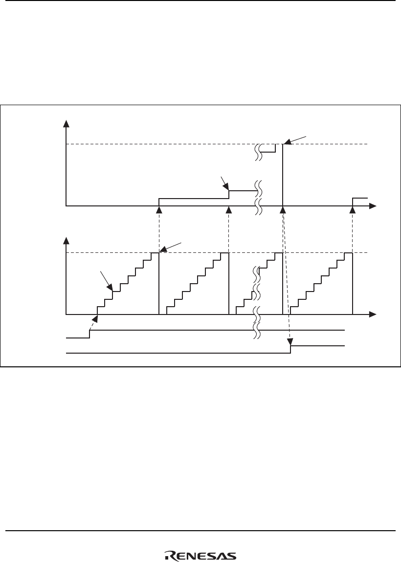
16. Watchdog Timer and Reset (WDT)
Rev.1.00 Jan. 10, 2008 Page 772 of 1658
REJ09B0261-0100
16.4.4 Time until WDT Counters Overflow
The relationship between WDTCNT and WDTBCNT is shown in figure 16.2. The example shown
in the figure is the operation in interval timer mode, where WDTCNT restarts counting after it has
overflowed. In watchdog timer mode, WDTCNT and WDTBCNT are cleared to 0 after the reset
state is exited and start counting up again.
WDTCNT value
WDTBCNT value
WDTST
H'0000 0000
H'0003 FFFF
H'0000 0000
Incremented every
peripheral clock (Pck)
cycle
Counting starts Flag is set Time
Time
TME
WOVF
IOVF
Incremented on each
WDTBCNT overflow
Cleared to 0
on overflow
Cleared to 0
on overflow
Figure 16.2 WDT Counting Operations (Example in Interval Timer Mode)

16. Watchdog Timer and Reset (WDT)
Rev.1.00 Jan. 10, 2008 Page 773 of 1658
REJ09B0261-0100
WDTBCNT is an 18-bit counter that is incremented by the peripheral clock. If the period of
peripheral clock Pck is represented as tPck (ns), the overflow time of WDTBCNT is expressed as
follows.
218 [bit] × tPck [ns] = 0.262 × tPck [ms]
WDTCNT is a 12-bit counter that is incremented each time WDTBCNT overflows. The time until
WDTCNT overflows becomes maximum when 0 is written to all the bits in WDTST. If the period
of peripheral clock Pck is represented as tPck (ns), the maximum overflow time of WDTCNT is
expressed as follows.
212 [bit] × (0.262 × tPck) [ms] = 1.073 × tPck [s]
The time until WDTCNT overflows becomes minimum when H'5A00 0001 is written to WDTST.
In this case, the overflow time is equal to that of WDTBCNT.
For example, if the peripheral clock frequency is 50 MHz, tPck is 20 ns and the overflow times are
as follows.
Overflow time of WDTBCNT: 0.262 × 20 = 5.24 [ms]
Maximum overflow time of WDTCNT: 1.073 × 20 = 21.46 [s]
16.4.5 Clearing WDT Counters
Setting the overflow value in WDTBST clears WDTBCNT to 0, and setting the overflow value in
WDTST clears WDTCNT to 0.
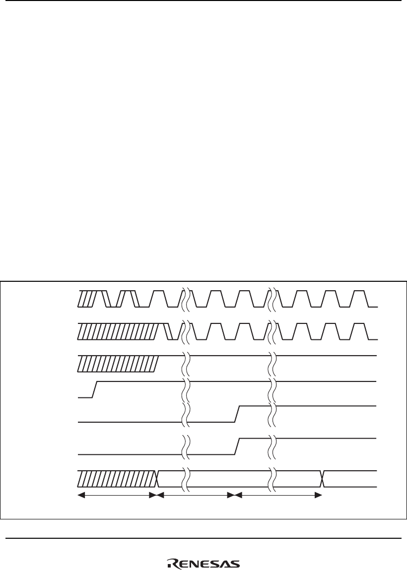
16. Watchdog Timer and Reset (WDT)
Rev.1.00 Jan. 10, 2008 Page 774 of 1658
REJ09B0261-0100
16.5 Status Pin Change Timing during Reset
16.5.1 Power-On Reset by PRESET Pin
Since the PLL circuit is initialized when the LSI enters the power-on reset state, the PLL
oscillation settling time needs to be ensured. This means that a high level must not be input to the
PRESET pin during the PLL oscillation settling time. The PLL oscillation settling time is the sum
of the settling times for PLL1 and PLL2.
After the state on the PRESET pin input is changed from a low level to high level, the internal
reset state continues until the reset holding time elapses. The reset holding time is equal to or more
than 40 cycles of the peripheral clock (Pck).
(1) When the Power Is Turned On
When the power is turned on, ensure that a low level is input to the PRESET pin. A low level
input is also needed on the TRST pin to initialize the H-UDI.
The timing of reset state indication on the STATUS[1:0] pins is asynchronous. On the other hand,
the timing of indicating normal operation is synchronous with the peripheral clock (Pck), and is
therefore asynchronous with the clocks input from the EXTAL pin and the CLKOUT pin.
VDD
TRST
input
PRESET
input
CLKOUT
output
STATUS[1:0]
output HH (reset) LL (normal)
EXTAL input
stabilization time PLL oscillation
settling time
Reset holding time
EXTAL
input
CLKOUTENB
output
Figure 16.3 STATUS Output when Power Is Turned On

16. Watchdog Timer and Reset (WDT)
Rev.1.00 Jan. 10, 2008 Page 775 of 1658
REJ09B0261-0100
(2) Power-On Reset Caused by PRESET Input during Normal Operation
It is necessary to ensure the PLL oscillation settling time when a power-on reset is initiated by low
level input on the PRESET pin during normal operation.
The timing of reset state indication on the STATUS[1:0] pins is asynchronous. The timing of
indicating normal operation is synchronous with the peripheral clock (Pck), and is therefore
asynchronous with the clocks input from the EXTAL pin and the CLKOUT pin.
CLKOUT
output
STATUS[1:0]
output HH (reset)HH (reset) LL (normal)LL (normal)
PLL oscillation
settling time Reset holding time
PRESET
input
EXTAL
input
CLKOUTENB
output
Figure 16.4 STATUS Output by Power-On Reset Caused by PRESET Input
during Normal Operation
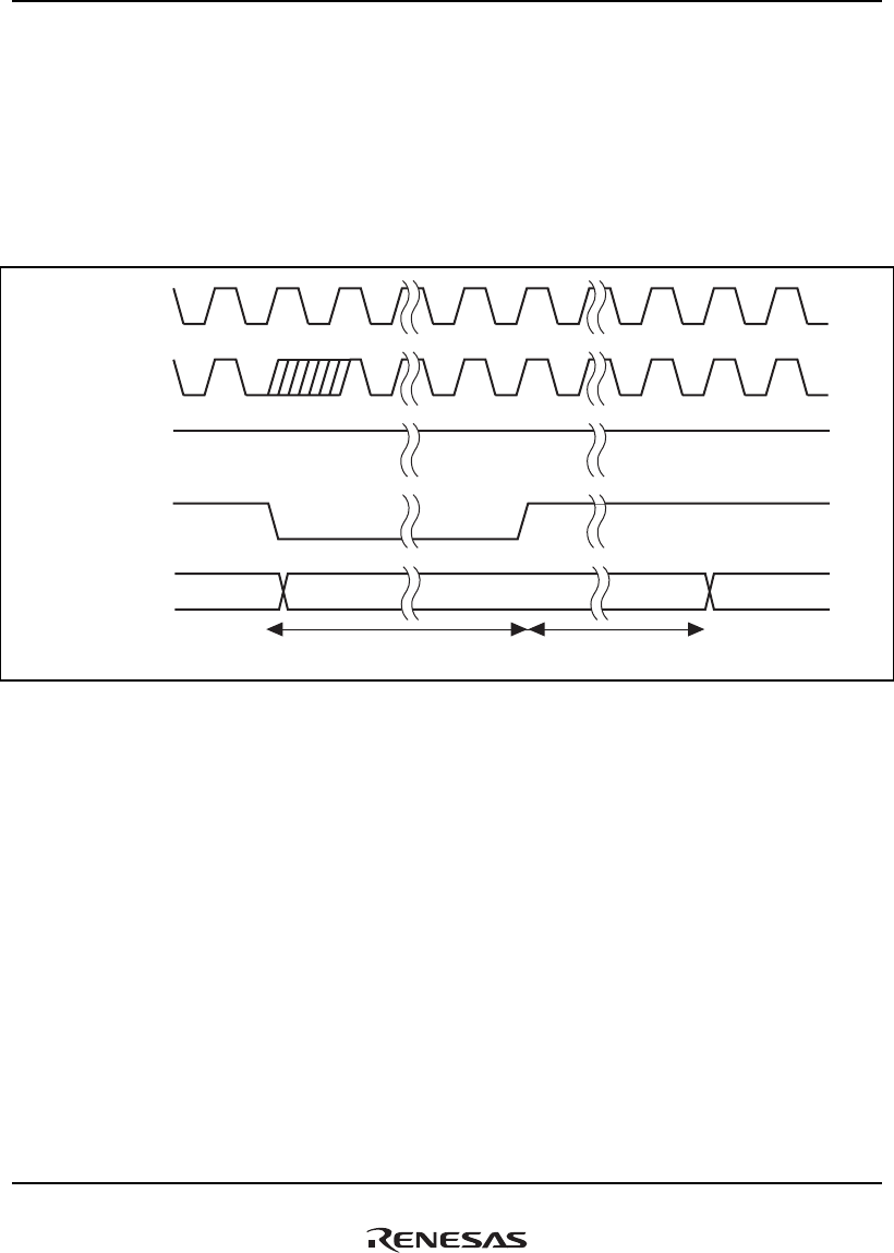
16. Watchdog Timer and Reset (WDT)
Rev.1.00 Jan. 10, 2008 Page 776 of 1658
REJ09B0261-0100
(3) Power-On Reset Caused by PRESET Input in Sleep Mode
It is necessary to ensure the PLL oscillation settling time when a power-on reset is initiated by a
low level input on the PRESET pin during sleep mode.
The timing of reset state indication on the STATUS[1:0] pins is asynchronous. The timing of
indicating normal operation is synchronous with the peripheral clock (Pck), and is therefore
asynchronous with the clocks input from the EXTAL pin and the CLKOUT pin.
CLKOUT
output
STATUS[1:0]
output HH (reset)HH (reset) LL (normal)HL (sleep)
PLL oscillation
settling time Reset holding time
PRESET
input
EXTAL
input
CLKOUTENB
output
Figure 16.5 STATUS Output by Power-On Reset Caused by PRESET Input
in Sleep Mode
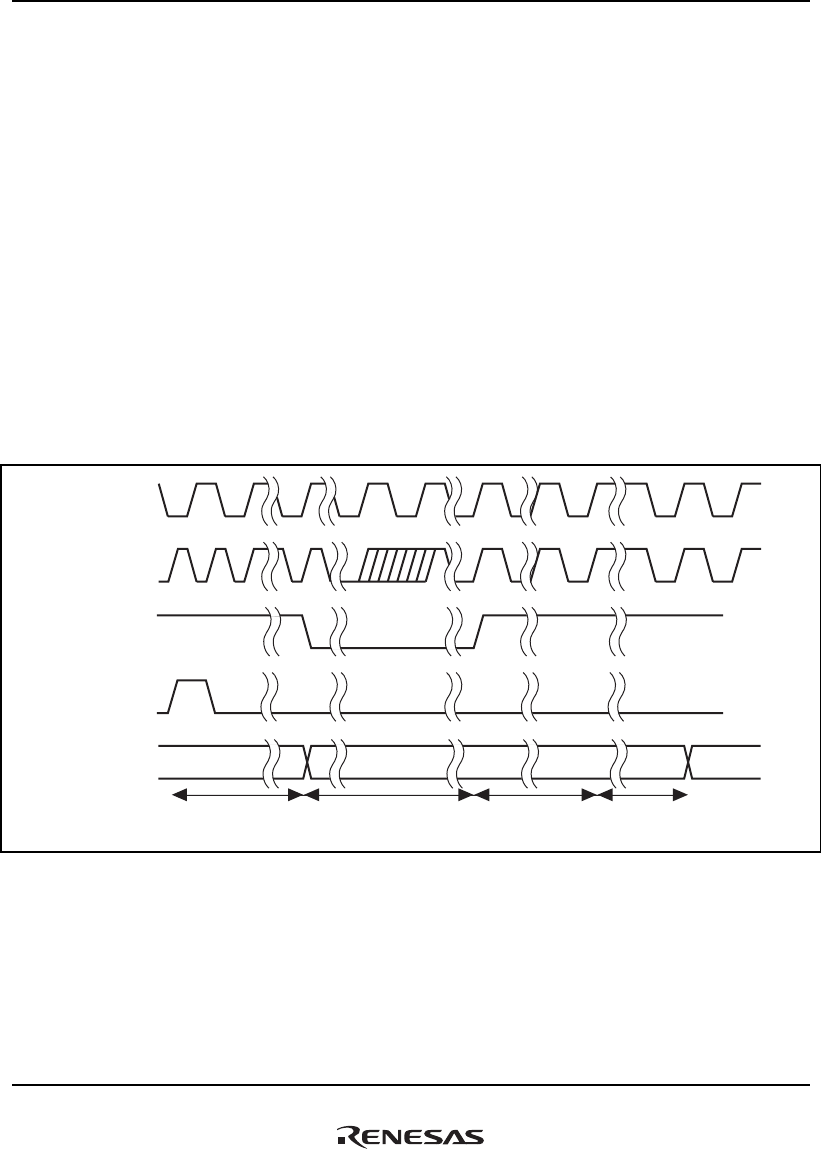
16. Watchdog Timer and Reset (WDT)
Rev.1.00 Jan. 10, 2008 Page 777 of 1658
REJ09B0261-0100
16.5.2 Power-On Reset by Watchdog Timer Overflow
The time period taken by power-on reset on watchdog timer overflow (WDT reset holding time) is
equal to or more than 40 cycles of the peripheral clock (Pck).
The transition time from watchdog timer overflow to the power-on reset state (WDT reset setup
time) is equal to or more than 40 cycles of the peripheral clock (Pck).
If the bus clock frequency has been changed from the initial value, the oscillation settling time of
PLL2 circuit and the time until the LSI resumes operation (WDT count up) are also required. In
this case, the WDT reset holding time is two peripheral clock (Pck) cycles or more.
(1) Power-On Reset Caused by Watchdog Timer Overflow during Normal Operation
The timing of indicating the reset state or normal operation on the STATUS[1:0] pins is
synchronous with the peripheral clock (Pck), and is therefore asynchronous with the clocks input
from the EXTAL pin and the CLKOUT pin.
WDT reset setup time WDT count up WDT reset
holding time
WDT overflow
signal
CLKOUT
output
STATUS[1:0]
output HH (reset) LL (normal)LL (normal)
PLL oscillation
settling time
EXTAL
input
CLKOUTENB
output
Figure 16.6 STATUS Output by Power-On Reset Caused by WDT Overflow
during Normal Operation
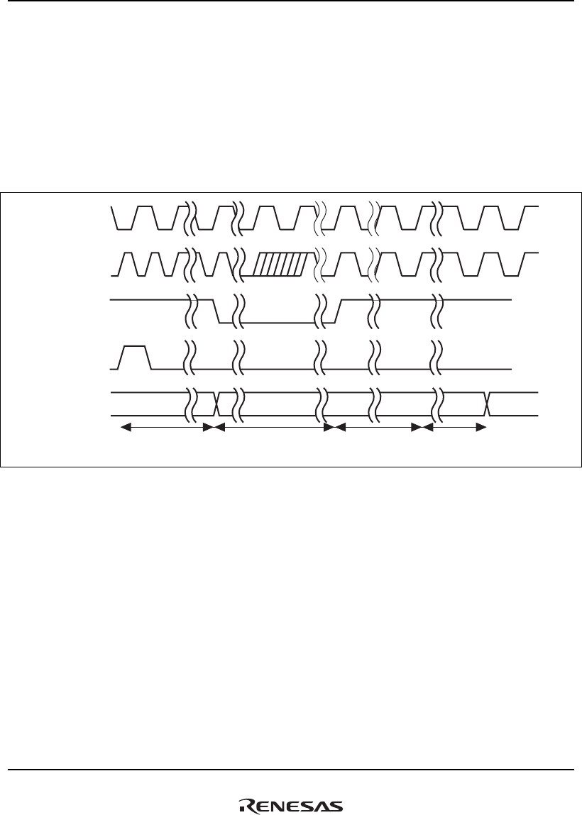
16. Watchdog Timer and Reset (WDT)
Rev.1.00 Jan. 10, 2008 Page 778 of 1658
REJ09B0261-0100
(2) Power-On Reset Caused by Watchdog Timer Overflow in Sleep Mode
The timing of indicating the reset state or normal operation on the STATUS[1:0] pins is
synchronous with the peripheral clock (Pck), and is therefore asynchronous with the clocks input
from the EXTAL pin and the CLKOUT pin.
If the bus clock frequency has been changed from the initial value, the oscillation settling time of
PLL2 circuit and the time until the LSI resumes operation (WDT count up) are also required. In
this case, the WDT reset holding time is two peripheral clock (Pck) cycles or more.
WDT reset setup time WDT count up WDT reset
holding time
WDT overflow
signal
CLKOUT
output
STATUS[1:0]
output HH (reset) LL (normal)HL (sleep)
PLL oscillation
settling time
EXTAL
input
CLKOUTENB
output
Figure 16.7 STATUS Output by Power-On Reset Caused by WDT Overflow
in Sleep Mode
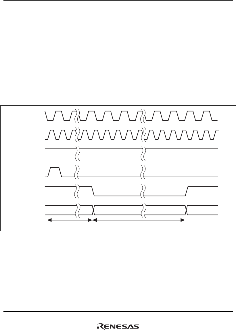
16. Watchdog Timer and Reset (WDT)
Rev.1.00 Jan. 10, 2008 Page 779 of 1658
REJ09B0261-0100
16.5.3 Manual Reset by Watchdog Timer Overflow
The time period taken by manual reset on watchdog timer overflow (WDT manual reset holding
time) is equal to or more than 30 cycles of the peripheral clock (Pck).
The transition time from watchdog timer overflow to the manual reset state (WDT reset setup
time) is equal to or more than eight cycles of the peripheral clock (Pck).
(1) Manual Reset Caused by Watchdog Timer Overflow during Normal Operation
The timing of indicating the reset state or normal operation on the STATUS[1:0] pins is
synchronous with the peripheral clock (Pck), and is therefore asynchronous with the clocks input
from the EXTAL pin and the CLKOUT pin.
WDT reset setup time WDT manual reset holding time
WDT overflow
signal
CLKOUT
output
STATUS[1:0]
output HH (reset) LL (normal)LL (normal)
EXTAL
input
CLKOUTENB
output
MRESETOUT
output
Figure 16.8 STATUS Output by Manual Reset Caused by WDT Overflow
during Normal Operation
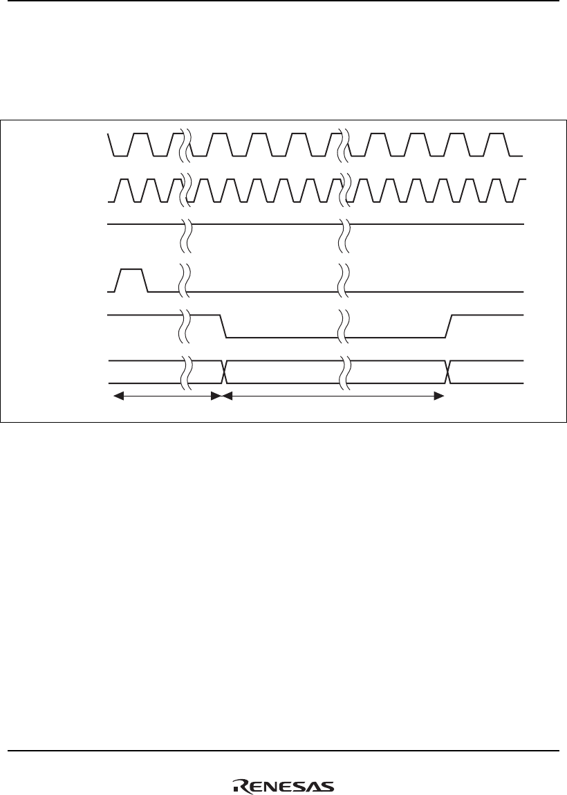
16. Watchdog Timer and Reset (WDT)
Rev.1.00 Jan. 10, 2008 Page 780 of 1658
REJ09B0261-0100
(2) Manual Reset Caused by Watchdog Timer Overflow in Sleep Mode
The timing of indicating the reset state or normal operation on the STATUS[1:0] pins is
synchronous with the peripheral clock (Pck), and is therefore asynchronous with the clocks input
from the EXTAL pin and the CLKOUT pin.
WDT reset setup time WDT manual reset holding time
WDT overflow
signal
CLKOUT
output
STATUS[1:0]
output HH (reset) LL (normal)HL (sleep)
EXTAL
input
CLKOUTENB
output
MRESETOUT
output
Figure 16.9 STATUS Output by Manual Reset Caused by WDT Overflow
in Sleep Mode

17. Power-Down Mode
Rev.1.00 Jan. 10, 2008 Page 781 of 1658
REJ09B0261-0100
Section 17 Power-Down Mode
In power-down mode, some of the on-chip modules and the CPU are stopped. This enables to
reduce power consumption.
17.1 Features
• Supports sleep mode, deep sleep mode, and module standby mode
• Supports DDR2-SDRAM power supply backup mode that turns off the power supplies the 1.8-
V power supply
17.1.1 Types of Power-Down Modes
Power-down modes have the following modes and functions.
• Sleep mode
• Deep sleep mode
• Module standby function
• DDR-SDRAM power supply backup
Table 17.1 shows the conditions of transition to each mode, the states of the CPU, on-chip
modules, etc. in each mode, and the methods for releasing each mode.

17. Power-Down Mode
Rev.1.00 Jan. 10, 2008 Page 782 of 1658
REJ09B0261-0100
Table 17.1 States of Power-Down Modes
State
On-Chip Peripheral Module
Power-
Down
Mode
Conditions of
Transition CPG CPU
On-Chip
Memory DMAC GDTA Others
Pin DDR2-SDRAM
Releasing
Methods
Sleep
mode
SLEEP
instruction
executed (see
section 17.4)
Operate Stopped
(contents
of registers
retained)
Retained Operate Operate Operate Operation
retained
Auto-refresh or
self-refresh*3
1. Interrupt
2. Power-on
reset
3. Manual
reset
Deep
sleep
mode
Corresponding
bit in MSTPCR
set to 1 (see
section 17.3.2)
Operate Stopped
(contents
of registers
retained)
Retained Stopped
(contents
of
registers
retained)
Stopped
(contents
of
registers
retained)
Operate
(DU,
TMU,
SCIF,
SIOF,
HSPI,
MMCIF,
HAC,
SSI,
FLCTL,
and UBC
are
stopped
*1)
Operation
retained
Self-refresh 1. Interrupt
2. Power-on
reset
3. Manual
reset
Module
standby
function
Clear the
corresponding
bits in
MSTPCR0 and
MSTPCR1 to 0
(see sections
17.3.2 and
17.3.3)
Operate Operate Retained Stopped
in six-
channel
units:
channels
0 to 5 and
channels
6 to 11.
Stopped Specified
modules
stopped
Operation
retained
Auto-refresh or
self-refresh
Clear the
corresponding
bits in
MSTPCR0 and
MSTPCR1 to 0
(see sections
17.3.2 and
17.3.3)
DDR2-
SDRAM
power
supply
backup *2
See section
17.7
Stopped Stopped Undefined Stopped Stopped Stopped Undefined
except for the
1.8-V power
supply
interface
(When the
MBKPRST is
low level input,
the MCKE is
high level
output)
Self-refresh Power-on
reset
Notes: 1. The TMU, SCIF, SIOF, HSPI, MMCIF, HAC, SSI, FLCTL and UBC should be in module
stop state by using the module standby function before execute the SLEEP instruction
to make transition to deep sleep mode. For detail, refer to section 17.5, Deep Sleep
Mode.
2. Power supplies (1.1 V, 3.3 V) except the 1.8 V power supply are stopped in DDR2-
SDRAM power supply backup mode. Therefore, all circuitry other than the pad of DDR2
interface are stopped, including DDR2 interface control unit, and the contents of
registers are not retained.
3. For details on auto-refresh and self-refresh operation, see section 12, DDR2-SDRAM
Interface (DBSC2).

17. Power-Down Mode
Rev.1.00 Jan. 10, 2008 Page 783 of 1658
REJ09B0261-0100
17.2 Input/Output Pins
Table 17.2 shows the pins related to power-down mode.
Table 17.2 Pin Configuration
Pin name Function I/O Description
STATUS1 Processing state 1 Output Indicate the operating states of this LSI
STATUS0 Processing state 2 STATUS1 STATUS0 Operating states
H H Reset
H L Sleep mode
L L Normal operation
The STATUS1 pin is multiplexed with the DRAK1
(DMAC) and PK6 (GPIO) pins. The STATUS0 pin
is multiplexed with the DRAK0 (DMAC) and PK7
(GPIO) pins.
Note: L means low level, and H means high level.
17.3 Register Descriptions
Table 17.3 shows the list of registers. Table 17.4 shows the register states in each processing
mode.
Table 17.3 Register Configuration
Table 17.3 Register Configuration
Register Name Abbreviation R/W P4 Address
Area 7
Address
Access
Size
Sync
clock
Sleep control register SLPCR R/W H'FFC8 0020 H'1FC8 0020 32 Pck
Standby control register 0 MSTPCR0 R/W H'FFC8 0030 H'1FC8 0030 32 Pck
Standby control register 1 MSTPCR1 R/W H'FFC8 0034 H'1FC8 0034 32 Pck
Standby display register MSTPMR R H'FFC8 0044 H'1FC8 0044 32 Pck
Note: For details of MSTPCR0 and MSTPCR1, see figure 15.1.

17. Power-Down Mode
Rev.1.00 Jan. 10, 2008 Page 784 of 1658
REJ09B0261-0100
Table 17.4 Register States of CPG in Each Processing Mode
Power-on Reset Manual Reset
Sleep/
Deep Sleep
Register Name Abbreviation
By PRESET
Pin/WDT/H-UDI By WDT
By SLEEP
Instruction
Standby control register 0*1 MSTPCR0 H'0000 0000 Retained Retained
Standby control register 1*1 MSTPCR1 H'0000 0000 Retained Retained
Standby display register MSTPMR H'00x0 0000∗2 Retained Retained
Notes: 1. For details of MSTPCR0 and MSTPCR1, see figure 15.1.
2. The initial value after a power-on reset depends on the combination of mode pin states
(MODE11 and MODE12).
If a low level signal is input to the MODE12 pin, the initial value is H'0010 0000.
If a high level signal is input to the MODE12 pin and a low level signal is input to
MODE11, the initial value is H'0030 0000.
If a high level signal is input to the MODE12 and MODE11 pins, the initial value is
H'0020 0000.

17. Power-Down Mode
Rev.1.00 Jan. 10, 2008 Page 785 of 1658
REJ09B0261-0100
17.3.1 Sleep Control Register (SLPCR)
SLPCR is a 32-bit readable/writable register that can specify transition to deep sleep mode.
SLPCR can be accessed only in longword.
This register is initialized by a power-on reset by the PRESET pin or power-on reset by WDT
overflow, or H-UDI reset.
161718192021222324252627282931 30
0000000000000000
⎯⎯⎯⎯⎯⎯⎯⎯⎯⎯⎯⎯⎯⎯⎯⎯
RRRRRRRRRRRRRRRR
BIt:
Initial value:
R/W:
01234567891011121315 14
0000000000000000
DSLP⎯⎯⎯⎯⎯⎯⎯⎯⎯⎯⎯⎯⎯⎯⎯
R/WR/WRRRRRRRRRRRRRR
BIt:
Initial value:
R/W:
Bit Bit Name
Initial
Value R/W Description
31 to 2 ⎯ All 0 R Reserved
These bits are always read as 0. The write value
should always be 0.
1 ⎯ 0 R/W Reserved
These bits are always read as 0. The write value
should always be 0.
0 DSLP 0 R/W Deep Sleep
Enables transition to deep sleep mode by the SLEEP
instruction
0: Transition to sleep mode by the SLEEP instruction
1: Transition to deep sleep mode by the SLEEP
instruction

17. Power-Down Mode
Rev.1.00 Jan. 10, 2008 Page 786 of 1658
REJ09B0261-0100
17.3.2 Standby Control Register 0 (MSTPCR0)
MSTPCR0 is a 32-bit readable/writable register that can specify whether each peripheral module
operates or is stopped. MSTPCR can be accessed only in longword.
This register is initialized by a power-on reset by the PRESET pin or power-on reset by WDT
overflow, or H-UDI reset.
161718192021222324252627282931 30
0000000000000000
MSTP[17:16]
⎯⎯
MSTP[21:20]
⎯⎯
MSTP[29:24]
⎯⎯
R/WR/WR/WR/WR/WR/WR/WR/WR/WR/WR/WR/WR/WR/WR/W R/W
BIt:
Initial value:
R/W:
01234567891011121315 14
0000000000000000
⎯⎯
MSTP[3:2]
⎯⎯⎯⎯
MSTP[9:8]
⎯⎯
MSTP[13:12]
⎯⎯
R/WR/WR/WR/WR/WR/WR/WR/WR/WR/WR/WR/WR/WR/WR/W R/W
BIt:
Initial value:
R/W:
Bit Bit Name
Initial
Value R/W Description
31, 30 ⎯ All 0 R/W Reserved
These bits are always read as 0. The write value
should always be 0.
29 to 24 MSTP[29:24] All 0 R/W Module Stop Bit [29:24]
Specify that the clock supply to the module of the
corresponding bit is stopped
[29]: SCIF channel 5, [28]: SCIF channel 4,
[27]: SCIF channel 3, [26]: SCIF channel 2,
[25]: SCIF channel 1, [24]: SCIF channel 0
0: The corresponding module operates
1: The clock to the corresponding module is
stopped
23, 22 ⎯ All 0 R/W Reserved
These bits are always read as 0. The write value
should always be 0.

17. Power-Down Mode
Rev.1.00 Jan. 10, 2008 Page 787 of 1658
REJ09B0261-0100
Bit Bit Name
Initial
Value R/W Description
21, 20 MSTP[21:20] All 0 R/W Module Stop Bit [21:20]
Specify that the clock supply to the module of the
corresponding bit is stopped
[21]: SSI channel 1, [20]: SSI channel 0
0: The corresponding module operates
1: The clock to the corresponding module is
stopped
19, 18 ⎯ All 0 R/W Reserved
These bits are always read as 0. The write value
should always be 0.
17, 16 MSTP[17:16] All 0 R/W Module Stop Bit [17:16]
Specify that the clock supply to the module of the
corresponding bit is stopped
[17]: HAC channel 1, [16] HAC channel 0
0: The corresponding module operates
1: The clock to the corresponding module is
stopped
15, 14 ⎯ All 0 R/W Reserved
These bits are always read as 0. The write value
should always be 0.
13, 12 MSTP[13:12] All 0 R/W Module Stop Bit [13:12]
Specify that the clock supply to the module of the
corresponding bit is stopped
[13]: MMCIF, [12] FLCTL
0: The corresponding module operates
1: The clock to the corresponding module is
stopped
11, 10 ⎯ All 0 R/W Reserved
These bits are always read as 0. The write value
should always be 0.

17. Power-Down Mode
Rev.1.00 Jan. 10, 2008 Page 788 of 1658
REJ09B0261-0100
Bit Bit Name
Initial
Value R/W Description
9, 8 MSTP[9:8] All 0 R/W Module Stop Bit [9:8]
Specify that the clock supply to the module of the
corresponding bit is stopped
[9]: TMU channels 3 to 5
[8]: TMU channels 2 to 0
0: The corresponding module operates
1: The clock to the corresponding module is
stopped
7 to 4 ⎯ All 0 R/W Reserved
These bits are always read as 0. The write value
should always be 0.
3, 2 MSTP[3:2] All 0 R/W Module Stop Bit [3:2]
Specify that the clock supply to the module of the
corresponding bit is stopped
[3]: SIOF, [2]: HSPI
0: The corresponding module operates
1: The clock to the corresponding module is
stopped
1, 0 ⎯ All 0 R/W Reserved
These bits are always read as 0. The write value
should always be 0.

17. Power-Down Mode
Rev.1.00 Jan. 10, 2008 Page 789 of 1658
REJ09B0261-0100
17.3.3 Standby Control Register 1 (MSTPCR1)
MSTPCR1 is a 32-bit readable/writable register that each module of H-UDI, UBC, DMAC, and
GDTA operates or is stopped. MSTPCR1 can be accessed only in longword.
This register is initialized by a power-on reset by the PRESET pin or power-on reset by WDT
overflow, or H-UDI reset.
161718192021222324252627282931 30
0000000000000000
⎯
MSTP117
⎯
MSTP119
⎯⎯⎯⎯⎯⎯⎯⎯⎯⎯⎯⎯
R/WR/WR/WR/WR/WR/WR/WR/WR/WR/WR/WR/WR/WR/WR/W R/W
BIt:
Initial value:
R/W:
01234567891011121315 14
0000000000000000
MSTP100
⎯⎯⎯
MSTP[105:104]
⎯⎯⎯⎯⎯⎯⎯⎯⎯⎯
R/WR/WR/WR/WR/WR/WR/WR/WR/WR/WR/WR/WR/WR/WR/W R/W
BIt:
Initial value:
R/W:
Bit Bit Name
Initial
Value R/W Description
31 to 20 ⎯ All 0 R/W Reserved
These bits are always read as 0. The write value
should always be 0.
19 MSTP119 0 R/W Module Stop Bit 119
Specifies that the clock supply to the H-UDI module is
stopped
0: H-UDI operates
1: H-UDI stopped
18 ⎯ 0 R/W Reserved
These bits are always read as 0. The write value
should always be 0.
17 MSTP117 0 R/W Module Stop Bit 117
Specifies that the clock supply to the UBC module is
stopped
0: UBC operates
1: UBC stopped

17. Power-Down Mode
Rev.1.00 Jan. 10, 2008 Page 790 of 1658
REJ09B0261-0100
Bit Bit Name
Initial
Value R/W Description
16 to 6 ⎯ All 0 R/W Reserved
These bits are always read as 0. The write value
should always be 0.
5, 4 MSTP
[105:104]
All 0 R/W Module Stop Bit [105:104]
Specifies that the clock supply to the DMAC channels
of the corresponding bit is stopped
MSTP105: DMAC channels 11 to 6,
MSTP104: DMAC channels 5 to 0
0: DMAC operates
1: DMAC stopped
3 to 1 ⎯ All 0 R/W Reserved
These bits are always read as 0. The write value
should always be 0.
0 MSTP100 0 R/W Module Stop Bit 100
Specifies that the clock supply to the GDTA module is
stopped
To stop the clock, set this bit to 1 after confirming that
the operation of GDTA is completed.
0: GDTA operates
1: GDTA stopped∗
Note: * The GDTA should be placed in module standby state after confirming that the operation
of the GDTA is completed. For the procedure, see section 20.7.1, Regarding Module
Stoppage.

17. Power-Down Mode
Rev.1.00 Jan. 10, 2008 Page 791 of 1658
REJ09B0261-0100
17.3.4 Standby Display Register (MSTPMR)
MSTPMR is a 32-bit readable register that indicates whether the PCIC/display unit
(DU)/DMAC/GDTA modules are in the module standby state. MSTPMR can be accessed only in
longword.
This register is initialized by a power-on reset by the PRESET pin, power-on reset by WDT
overflow, or H-UDI reset.
161718192021222324252627282931 30
0000xx0000000000
⎯⎯⎯⎯
MSTP
MDU
MSTP
MPCI
⎯⎯⎯⎯⎯⎯⎯⎯⎯⎯
RRRRRRRRRRRRRRRR
BIt:
Initial value:
R/W:
01234567891011121315 14
0000000000000000
MSTPS
100
⎯⎯⎯
MSTPS
104
MSTPS
105
⎯⎯⎯⎯⎯⎯⎯⎯⎯⎯
RRRRRRRRRRRRRRRR
BIt:
Initial value:
R/W:
Bit Bit Name
Initial
Value R/W Description
31 to 22 ⎯ All 0 R Reserved
These bits are always read as 0. The write value
should always be 0.
21 MSTPMPCI x R Module Stop Display Bit PCIC
Indicates the state of clock supply to the PCIC module
When a high level signal is input to the MODE12 pin,
the clock supply to the PCIC is stopped
0: PCIC operates (MODE12 pin: Low level)
1: PCIC stopped (MODE12 pin: High level)
20 MSTPMDU x R Module Stop Display Bit DU
Indicates the state of clock supply to the DU module.
When a low level signal is input to the MODE12 or
MODE11 pin, the clock supply to the DU is stopped.
0: DU operates (MODE[12:11] pin: All High level)
1: DU stopped (MODE[12:11] pin: Not all High level)
19 to 6 ⎯ All 0 R Reserved
These bits are always read as 0. The write value
should always be 0.

17. Power-Down Mode
Rev.1.00 Jan. 10, 2008 Page 792 of 1658
REJ09B0261-0100
Bit Bit Name
Initial
Value R/W Description
5, 4 MSTPS105
MSTPS104
All 0 R Module Stop Display Bit 105, 104
Indicates the state of clock supply to the DMAC
channels of the corresponding bit
MSTPS105: DMAC channels 11 to 6
MSTPS104: DMAC channels 5 to 0
0: The DMAC channels operate
1: The DMAC channels stopped
3 to 1 ⎯ All 0 R Reserved
These bits are always read as 0. The write value
should always be 0.
0 MSTP100 0 R Module Stop Display Bit 100
Indicates the state of clock supply to the GDTA
module
0: GDTA operates
1: GDTA stopped

17. Power-Down Mode
Rev.1.00 Jan. 10, 2008 Page 793 of 1658
REJ09B0261-0100
17.4 Sleep Mode
17.4.1 Transition to Sleep Mode
When the SLEEP instruction is executed, the state is changed from the program execution state to
sleep mode. Although the CPU is stopped after the instruction is executed, the contents of the
CPU register are retained.
On-chip modules other than the CPU continue to operate. The clock is output to the CLKOUT pin.
In sleep mode, a high level signal is output to the STATUS1 pin, and a low level signal is output
to the STATUS0 pin.
Complete the operation of DU before transition to sleep mode. Confirm that the operation of
GDTA is completed. The operation is not guaranteed if transition to sleep mode is performed
while the module is operating.
17.4.2 Releasing Sleep Mode
Sleep mode is released by interrupts (NMI, IRQ/IRL[7:0], and on-chip module) and reset.
In sleep mode, interrupts are accepted even if the BL bit in the SR register is 1. If needed, put
SPC, SSR, etc to stack before executing the SLEEP instruction.
(1) Release by Interrupts
When the NMI, IRQ/IRL[7:0], and on-chip module interrupts are generated, sleep mode is
released and exception handling of interrupts are performed. The code corresponding to the
interrupt sources is set to the INTEVT register.
For details of the timing of the changes in the STATUS pin, see section 17.7.2, Releasing Sleep
Mode.
(2) Release by a Reset
Sleep mode is released by a power-on reset by the PRESET pin, power-on reset by WDT
overflow, H-UDI reset, and manual reset. For details of the timing of the changes in the STATUS
pin, see section 16.5, Status Pin Change Timing during Reset.

17. Power-Down Mode
Rev.1.00 Jan. 10, 2008 Page 794 of 1658
REJ09B0261-0100
17.5 Deep Sleep Mode
17.5.1 Transition to Deep Sleep Mode
If a SLEEP instruction is executed when the DSLP bit in SLPCR is set to 1, the chip switches
from the program execution state to deep sleep mode. The procedure for a transition to deep sleep
mode is as follows:
1. Make each modules stop by setting standby control registers MSTPCR0 and MSTPCR1 except
the H-UDI module, i.e. write H’3F33 330C to MSTPCR0 and write H’0002 0031 to MSTPCR1.
For the note of the transition to module standby mode, see section 17.6.1, Transition to Module
Standby Mode and each module sections.
2. Execute a SLEEP instruction when the DSLP bit in SLPCR.
After execution of the SLEEP instruction, the CPU halts but its register contents are retained. The
DU is stopped* as well as the modules that were stopped by the module standby function. Except
for the DMAC, peripheral modules continue to operate. The clock continues to be output to the
CKIO pin, but all bus access (including auto refresh) stops. When using memory that requires
refreshing, select self-refreshing mode prior to making the transition to deep sleep mode.
Note: * For the transition to deep sleep mode of the DU, PCIC, LBSC and DBSC, see notes of
the transition to deep sleep mode in each module sections.
In deep sleep mode, a high-level signal is output at the STATUS1 pin, and a low-level signal at
the STATUS0 pin.
When using the PCIC, it is prohibited to make a transition to deep sleep mode. If transition to deep
sleep mode, the operation of the PCIC is not guaranteed.
If making a transition to deep sleep mode while each modules are in operation, the results of those
operation cannot be guaranteed.

17. Power-Down Mode
Rev.1.00 Jan. 10, 2008 Page 795 of 1658
REJ09B0261-0100
17.5.2 Releasing Deep Sleep Mode
Deep sleep mode is released by means of an interrupt (NMI, IRL, IRQ, GPIO, WDT interval
timer, or H-UDI) or a reset.
In deep sleep mode, an interrupt request is accepted even if the BL bit in SR is set to 1. The
SPC, SSR and other related contents should be saved before execute a SLEEP instruction if
necessary.
(1) Release by Interrupt
When an NMI, IRL, IRQ, GPIO, or WDT interval timer interrupt is generated, deep sleep mode is
released and the interrupt exception handling is executed. The code corresponding to the interrupt
source is set in INTEVT. For details of the timing of the changes in the STATUS pin, that is
similar to sleep mode, see section 17.7.2, Releasing Sleep Mode.
(2) Release by Reset
Deep sleep mode is released by means of a power-on via the PRESET pin or a WDT overflow, H-
UDI reset, or a manual reset by a WDT overflow. For details of the timing of the changes in the
STATUS pin, that is similar to sleep mode, see section 16.5, Status Pin Change Timing during
Reset.

17. Power-Down Mode
Rev.1.00 Jan. 10, 2008 Page 796 of 1658
REJ09B0261-0100
17.6 Module Standby Functions
This LSI supports the module standby state, where the clock supplied to on-chip modules is
stopped.
17.6.1 Transition to Module Standby Mode
By setting the MSTP bits in MSPTCR, the clock supply can be stopped to the corresponding
module*.
In each module that is in the module standby state, the state right before transition to module
standby state is retained. After register setting, the state right before stop is retained. The state of
the external pin is retained. When the module is released from the module standby state, the
module resumes operation.
SSI, HSPI, HAC, and MMCIF are initialized by a manual reset even if they are in the module
standby state. Confirm that the operation of GDTA is completed before putting GDTA and
DMAC in the module standby state.
Note: * For details of the description of the individual MSTP bits in the standby control
registers, see section 17.3.2, Standby Control Register 0 (MSTPCR0) and 17.3.3,
Standby Control Register 1 (MSTPCR1).
The MSTP bits should be set to 1 while the module is in the idle state after completing
its operation and there is no possible activation sources from external pins or other
modules.
17.6.2 Releasing Module Standby Functions
The module standby functions are released by clearing the MSTP bits in MSTPCR0 to 0 or a
power-on reset.
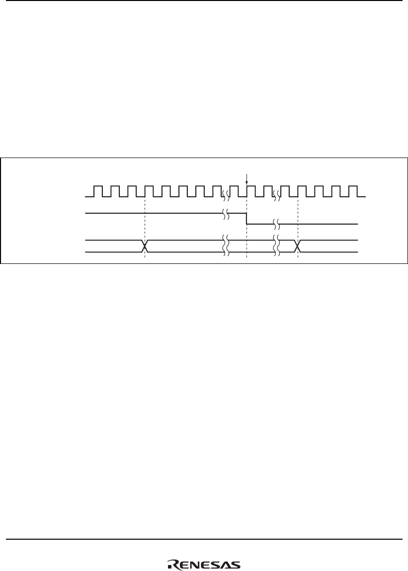
17. Power-Down Mode
Rev.1.00 Jan. 10, 2008 Page 797 of 1658
REJ09B0261-0100
17.7 Timing of the Changes on the STATUS Pins
17.7.1 Reset
For details, see section 16.5, Status Pin Change Timing during Reset.
17.7.2 Releasing Sleep Mode
(1) When Sleep Mode Is Released by an Interrupt
Figure 17.1 shows the timing of the changes in the STATUS pin.
Interrupt request
LL (Normal) HL (Sleep) LL (Normal)
CLKOUT
IRQOUT
output
STATUS[1:0]
output
Figure 17.1 Status Pins Output when an Interrupt Occurs in Sleep Mode
17.8 DDR-SDRAM Power Supply Backup
For details, see section 12.5.10, DDR2-SDRAM Power Supply Backup Function.

17. Power-Down Mode
Rev.1.00 Jan. 10, 2008 Page 798 of 1658
REJ09B0261-0100

18. Timer Unit (TMU)
Rev.1.00 Jan. 10, 2008 Page 799 of 1658
REJ09B0261-0100
Section 18 Timer Unit (TMU)
This LSI includes an on-chip 32-bit timer unit (TMU), which has six channels (channels 0 to 5).
18.1 Features
The TMU has the following features.
• Auto-reload type 32-bit down-counter provided for each channel
• Input capture function provided only for channel 2
• Selection of rising edge or falling edge as external clock input edge when external clock is
selected or input capture function is used: Channels 0 to 2
• 32-bit timer constant register for auto-reload use, readable/writable at any time, and 32-bit
down-counter provided for each channel
• Selection of six counter input clocks: Channels 0 to 2
External clock (TCLK) and five internal clocks (Pck/4, Pck/16, Pck/64, Pck/256, and
Pck/1024) obtained by dividing the peripheral clock (Pck is the peripheral clock).
• Selection of five counter input clocks: Channels 3 to 5
Five internal clocks (Pck/4, Pck/16, Pck/64, Pck/256, and Pck/1024) (Pck is the peripheral
clock).
• Two interrupt sources
One underflow source (each channel) and one input capture source (channel 2).
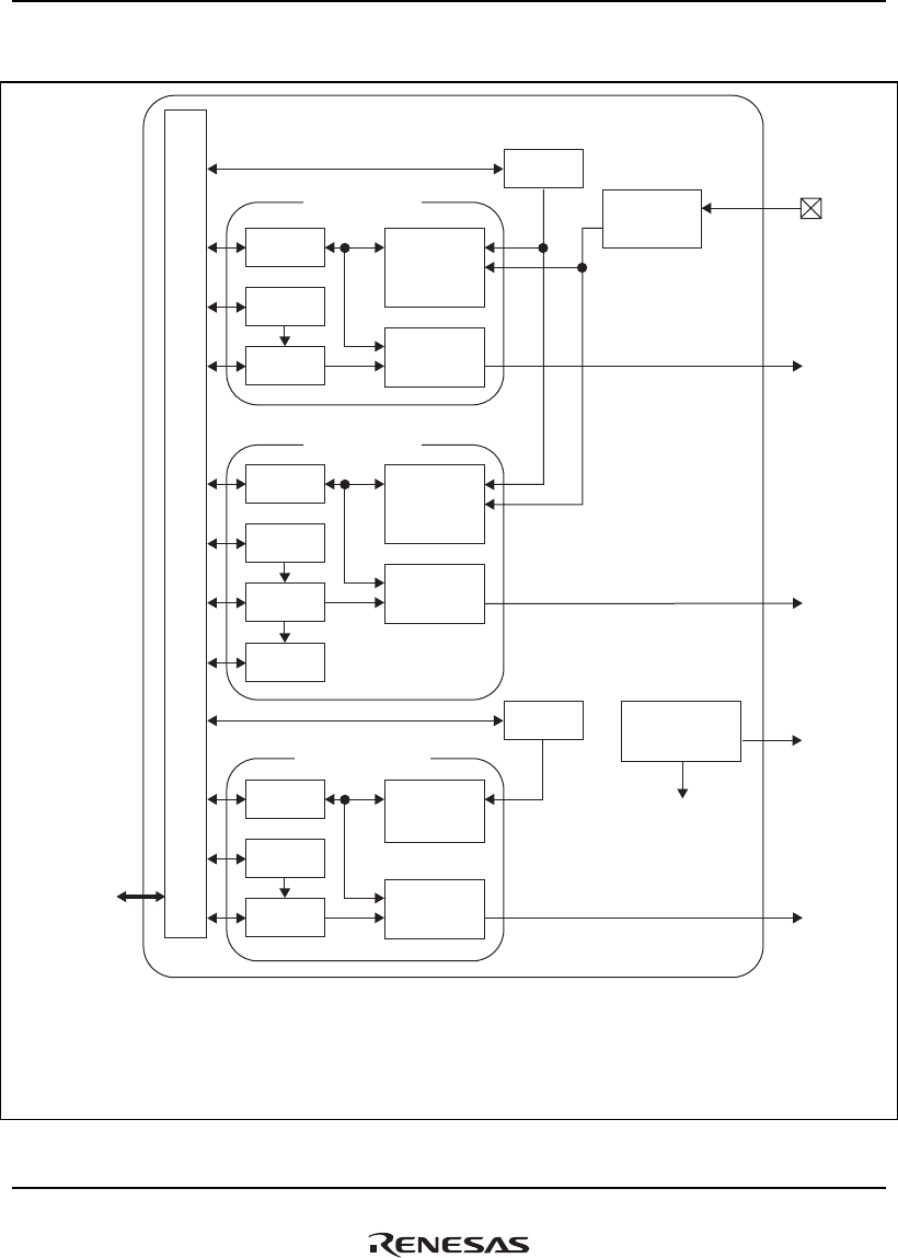
18. Timer Unit (TMU)
Rev.1.00 Jan. 10, 2008 Page 800 of 1658
REJ09B0261-0100
Figure 18.1 shows a block diagram of the TMU.
Channel 0, 1
Channel 2
Channel 3, 4, 5
TCR
TSTR0
TSTR1
Clock
controller
TCLK
controller
TCLK
TUNI0
TUNI1
TUNI2
ICPI2
Pck/4
Pck/16
Pck/64
TUNI3
TUNI4
TUNI5
Prescaler
To each
channel
Interrupt
controller
Clock
controller
Interrupt
controller
Clock
controller
Interrupt
controller
TCOR
TCNT
TCR
TCOR
TCNT
TCR
Peripheral
bus
TCOR
TCNT
TCPR2
Bus interface
Legend:
TCNT:
TCOR:
TCPR2:
TCR:
TSTR0, TSTR1:
Timer counter
Timer constant register
Input capture register 2 (channel 2 only)
Timer control register
Timer start register
Figure 18.1 Block Diagram of TMU

18. Timer Unit (TMU)
Rev.1.00 Jan. 10, 2008 Page 801 of 1658
REJ09B0261-0100
18.2 Input/Output Pins
Table 18.1 shows the TMU pin configuration.
Table 18.1 Pin Configuration
Pin Name Abbrev. I/O Description
Clock input TCLK Input External clock input pin for channels 0, 1 and 2
/input capture control input pin for channel 2

18. Timer Unit (TMU)
Rev.1.00 Jan. 10, 2008 Page 802 of 1658
REJ09B0261-0100
18.3 Register Descriptions
Tables 18.2 and 18.3 show the TMU register configuration.
Table 18.2 Register Configuration (1)
Channel Register Name Abbrev. R/W P4 Address Area 7 Address Size
Sync
Clock
Common
to 0, 1, 2
Timer start register 0 TSTR0 R/W H'FFD8 0004 H'1FD8 0004 8 Pck
Timer constant register 0 TCOR0 R/W H'FFD8 0008 H'1FD8 0008 32 Pck
Timer counter 0 TCNT0 R/W H'FFD8 000C H'1FD8 000C 32 Pck
0
Timer control register 0 TCR0 R/W H'FFD8 0010 H'1FD8 0010 16 Pck
Timer constant register 1 TCOR1 R/W H'FFD8 0014 H'1FD8 0014 32 Pck
Timer counter 1 TCNT1 R/W H'FFD8 0018 H'1FD8 0018 32 Pck
1
Timer control register 1 TCR1 R/W H'FFD8 001C H'1FD8 001C 16 Pck
Timer constant register 2 TCOR2 R/W H'FFD8 0020 H'1FD8 0020 32 Pck
Timer counter 2 TCNT2 R/W H'FFD8 0024 H'1FD8 0024 32 Pck
Timer control register 2 TCR2 R/W H'FFD8 0028 H'1FD8 0028 16 Pck
2
Input capture register 2 TCPR2 R H'FFD8 002C H'1FD8 002C 32 Pck
Common
to 3, 4, 5
Timer start register 1 TSTR1 R/W H'FFDC 0004 H'1FDC 0004 8 Pck
Timer constant register 3 TCOR3 R/W H'FFDC 0008 H'1FDC 0008 32 Pck
Timer counter 3 TCNT3 R/W H'FFDC 000C H'1FDC 000C 32 Pck
3
Timer control register 3 TCR3 R/W H'FFDC 0010 H'1FDC 0010 16 Pck
Timer constant register 4 TCOR4 R/W H'FFDC 0014 H'1FDC 0014 32 Pck
Timer counter 4 TCNT4 R/W H'FFDC 0018 H'1FDC 0018 32 Pck
4
Timer control register 4 TCR4 R/W H'FFDC 001C H'1FDC 001C 16 Pck
5 Timer constant register 5 TCOR5 R/W H'FFDC 0020 H'1FDC 0020 32 Pck
Timer counter 5 TCNT5 R/W H'FFDC 0024 H'1FDC 0024 32 Pck
Timer control register 5 TCR5 R/W H'FFDC 0028 H'1FDC 0028 16 Pck

18. Timer Unit (TMU)
Rev.1.00 Jan. 10, 2008 Page 803 of 1658
REJ09B0261-0100
Table 18.3 Register Configuration (2)
Channel Register Name Abbrev.
Power-on
Reset by
PRESET Pin/
WDT/H-UDI
Manual Reset
by WDT/
Multiple
Exceptions
Sleep by
SLEEP
Instruction
Module
Standby
Common
to 0, 1, 2
Timer start register 0 TSTR0 H'00 H'00 Retained Retained
Timer constant register 0 TCOR0 H'FFFF FFFF H'FFFF FFFF Retained Retained
Timer counter 0 TCNT0 H'FFFF FFFF H'FFFF FFFF Retained Retained
0
Timer control register 0 TCR0 H'0000 H'0000 Retained Retained
Timer constant register 1 TCOR1 H'FFFF FFFF H'FFFF FFFF Retained Retained
Timer counter 1 TCNT1 H'FFFF FFFF H'FFFF FFFF Retained Retained
1
Timer control register 1 TCR1 H'0000 H'0000 Retained Retained
Timer constant register 2 TCOR2 H'FFFF FFFF H'FFFF FFFF Retained Retained
Timer counter 2 TCNT2 H'FFFF FFFF H'FFFF FFFF Retained Retained
Timer control register 2 TCR2 H'0000 H'0000 Retained Retained
2
Input capture register 2 TCPR2 Retained Retained Retained Retained
Common
to 3, 4, 5
Timer start register 1 TSTR1 H'00 H'00 Retained Retained
Timer constant register3 TCOR3 H'FFFF FFFF H'FFFF FFFF Retained Retained
Timer counter 3 TCNT3 H'FFFF FFFF H'FFFF FFFF Retained Retained
3
Timer control register 3 TCR3 H'0000 H'0000 Retained Retained
Timer constant register 4 TCOR4 H'FFFF FFFF H'FFFF FFFF Retained Retained
Timer counter 4 TCNT4 H'FFFF FFFF H'FFFF FFFF Retained Retained
4
Timer control register 4 TCR4 H'0000 H'0000 Retained Retained
5 Timer constant register 5 TCOR5 H'FFFF FFFF H'FFFF FFFF Retained Retained
Timer counter 5 TCNT5 H'FFFF FFFF H'FFFF FFFF Retained Retained
Timer control register 5 TCR5 H'0000 H'0000 Retained Retained

18. Timer Unit (TMU)
Rev.1.00 Jan. 10, 2008 Page 804 of 1658
REJ09B0261-0100
18.3.1 Timer Start Registers (TSTRn) (n = 0, 1)
The TSTR registers are 8-bit readable/writable registers that specifies whether TCNT of the
corresponding channel is operated or stopped.
• TSTR0
01234567
00000000
STR0STR1STR2—————
R/WR/WR/WRRRRR
BIt:
Initial value:
R/W:
Bit Bit Name
Initial
Value R/W Description
7 to 3 — All 0 R Reserved
These bits are always read as 0. The write value should
always be 0.
2 STR2 0 R/W Counter Start 2
Specifies whether TCNT2 is operated or stopped.
0: TCNT2 count operation is stopped
1: TCNT2 performs count operation
1 STR1 0 R/W Counter Start 1
Specifies whether TCNT1 is operated or stopped.
0: TCNT1 count operation is stopped
1: TCNT1 performs count operation
0 STR0 0 R/W Counter Start 0
Specifies whether TCNT0 is operated or stopped.
0: TCNT0 count operation is stopped
1: TCNT0 performs count operation

18. Timer Unit (TMU)
Rev.1.00 Jan. 10, 2008 Page 805 of 1658
REJ09B0261-0100
• TSTR1
01234567
00000000
STR3STR4STR5—————
R/WR/WR/WRRRRR
BIt:
Initial value:
R/W:
Bit Bit Name
Initial
Value R/W Description
7 to 3 — All 0 R Reserved
These bits are always read as 0. The write value should
always be 0.
2 STR5 0 R/W Counter Start 5
Specifies whether TCNT5 is operated or stopped.
0: TCNT5 count operation is stopped
1: TCNT5 performs count operation
1 STR4 0 R/W Counter Start 4
Specifies whether TCNT4 is operated or stopped.
0: TCNT4 count operation is stopped
1: TCNT4 performs count operation
0 STR3 0 R/W Counter Start 3
Specifies whether TCNT3 is operated or stopped.
0: TCNT3 count operation is stopped
1: TCNT3 performs count operation

18. Timer Unit (TMU)
Rev.1.00 Jan. 10, 2008 Page 806 of 1658
REJ09B0261-0100
18.3.2 Timer Constant Registers (TCORn) (n = 0 to 5)
The TCOR registers are 32-bit readable/writable registers. When a TCNT counter underflows
while counting down, the TCOR value is set in that TCNT, which continues counting down from
the set value.
161718192021222324252627282931 30
1111111111111111
1111111111111111
R/WR/WR/WR/WR/WR/WR/WR/WR/WR/WR/WR/WR/WR/WR/W R/W
R/WR/WR/WR/WR/WR/WR/WR/WR/WR/WR/WR/WR/WR/WR/W R/W
BIt:
Initial value:
R/W:
01234567891011121315 14BIt:
Initial value:
R/W:
18.3.3 Timer Counters (TCNTn) (n = 0 to 5)
The TCNT registers are 32-bit readable/writable registers. Each TCNT counts down on the input
clock selected by the TPSC2 to TPSC0 bits in TCR.
When a TCNT counter underflows while counting down, the UNF flag is set in TCR of the
corresponding channel. At the same time, the TCOR value is set in TCNT, and the count-down
operation continues from the set value.
161718192021222324252627282931 30
1111111111111111
1111111111111111
R/WR/WR/WR/WR/WR/WR/WR/WR/WR/WR/WR/WR/WR/WR/W R/W
R/WR/WR/WR/WR/WR/WR/WR/WR/WR/WR/WR/WR/WR/WR/W R/W
BIt:
Initial value:
R/W:
01234567891011121315 14BIt:
Initial value:
R/W:

18. Timer Unit (TMU)
Rev.1.00 Jan. 10, 2008 Page 807 of 1658
REJ09B0261-0100
18.3.4 Timer Control Registers (TCRn) (n = 0 to 5)
The TCR registers are 16-bit readable/writable registers. Each TCR selects the count clock,
specifies the edge when an external clock is selected, and controls interrupt generation when the
flag indicating TCNT underflow is set to 1. TCR2 is also used for input capture control and
control of interrupt generation in the event of input capture.
• TCR0, TCR1, TCR3, TCR4 and TCR5
01234567891011121315 14
0000000000000000
TPSC0TPSC1TPSC2CKEG0CKEG1UNIE——UNF———————
R/WR/WR/WR/WR/WR/WRRR/WRRRRRRR
BIt:
Initial value:
R/W:
• TCR2
01234567891011121315 14
0000000000000000
TPSC0TPSC1TPSC2CKEG0CKEG1UNIEICPE0ICPE1UNFICPF——————
R/WR/WR/WR/WR/WR/WR/WR/WR/WR/WRRRRRR
BIt:
Initial value:
R/W:
Bit Bit Name
Initial
Value R/W Description
15 to 10 — All 0 R Reserved
These bits are always read as 0. The write value should
always be 0.
9 ICPF*1 0 R/W Input Capture Interrupt Flag
Status flag, provided in channel 2 only, which indicates
the occurrence of input capture.
0: Input capture has not occurred
[Clearing condition]
When 0 is written to ICPF
1: Input capture has occurred
[Setting condition]
When input capture occurs*2
8 UNF 0 R/W Underflow Flag
Status flag that indicates the occurrence of TCNT
underflow.
0: TCNT has not underflowed
[Clearing condition]
When 0 is written to UNF
1: TCNT has underflowed
[Setting condition]
When TCNT underflows*2

18. Timer Unit (TMU)
Rev.1.00 Jan. 10, 2008 Page 808 of 1658
REJ09B0261-0100
Bit Bit Name
Initial
Value R/W Description
7
6
ICPE1*1
ICPE0*1
0
0
R/W
R/W
Input Capture Control
These bits, provided in channel 2 only, specify whether
the input capture function is used, and control enabling
or disabling of interrupt generation when the function is
used.
The CKEG bits specify whether the rising edge or falling
edge of the TCLK pin is used to set the TCNT2 value in
TCPR2.
The TCNT2 value is set in TCPR2 only when the ICPF
bit in TCR2 is 0. When the ICPF bit is 1, TCPR2 is not
set in the event of input capture.
00: Input capture function is not used.
01: Reserved (setting prohibited)
10: Input capture function is used, but interrupt due to
input capture (TICPI2) is not enabled.
11: Input capture function is used, and interrupt due to
input capture (TICPI2) is enabled.
5 UNIE 0 R/W Underflow Interrupt Control
Controls enabling or disabling of interrupt generation
when the UNF status flag is set to 1, indicating TCNT
underflow.
0: Interrupt due to underflow (TUNI) is disabled
1: Interrupt due to underflow (TUNI) is enabled
4
3
CKEG1
CKEG0
0
0
R/W
R/W
Clock Edge 1 and 0
These bits select the external clock input edge when an
external clock that is input from the TCLK pin is selected
or the input capture function is used.
00: Count/input capture register set on rising edge
01: Count/input capture register set on falling edge
1X: Count/input capture register set on both rising and
falling edges

18. Timer Unit (TMU)
Rev.1.00 Jan. 10, 2008 Page 809 of 1658
REJ09B0261-0100
Bit Bit Name
Initial
Value R/W Description
2
1
0
TPSC2
TPSC1
TPSC0
0
0
0
R/W
R/W
R/W
Timer Prescaler 2 to 0
These bits select the TCNT count clock.
000: Counts on Pck/4
001: Counts on Pck/16
010: Counts on Pck/64
011: Counts on Pck/256
100: Counts on Pck/1024
101, 110: Setting prohibited
111: Counts on external clock (TCLK) *3
Legend:
X: Don't care
Notes: 1. Reserved bit in channels 0 to 5 (initial value is 0, and can only be read).
2. Writing 1 does not change the value; the previous value is retained.
3. Do not set in channels 3, 4, and 5.
18.3.5 Input Capture Register 2 (TCPR2)
TCPR2 is a 32-bit read-only register for use with the input capture function, provided only in
channel 2. The input capture function is controlled by means of the ICPE and CKEG bits in TCR2.
When input capture occurs, the TCNT2 value is copied into TCPR2. The value is set in TCPR2
only when the ICPF bit in TCR2 is 0.
161718192021222324252627282931 30BIt:
Initial value:
R/W:
01234567891011121315 14BIt:
Initial value:
R/W:
————————————————
RRRRRRRRRRRRRRRR
————————————————
RRRRRRRRRRRRRRRR
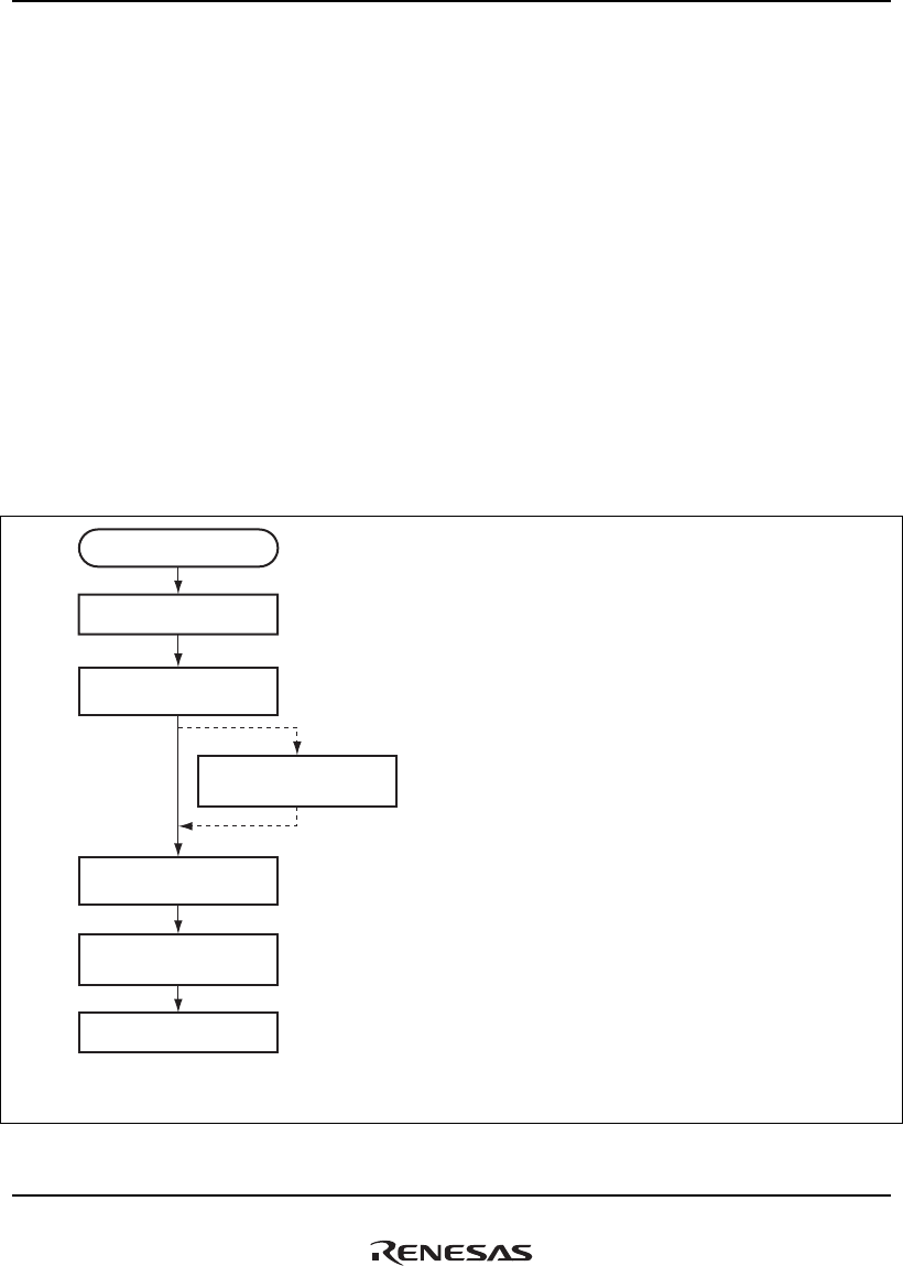
18. Timer Unit (TMU)
Rev.1.00 Jan. 10, 2008 Page 810 of 1658
REJ09B0261-0100
18.4 Operation
Each channel has a 32-bit timer counter (TCNT) and a 32-bit timer constant register (TCOR).
Each TCNT performs count-down operation. The channels have an auto-reload function that
allows cyclic count operations, and can also perform external event counting. Channel 2 also has
an input capture function.
18.4.1 Counter Operation
When one of bits STR0 to STR2 in TSTR is set to 1, the TCNT for the corresponding channel
starts counting. When TCNT underflows, the UNF flag in TCR is set. If the UNIE bit in TCR is
set to 1 at this time, an interrupt request is sent to the CPU. At the same time, the value is copied
from TCOR into TCNT, and the count-down continues (auto-reload function).
(1) Example of Counter Operation Setting Procedure
Figure 18.2 shows an example of the counter operation setting procedure.
Counter operation setup
Select counter clock
Set up underflow
interrupt generation
Set up input capture
interrupt generation
When using
input capture
function
Set timer constant
register
Load the counter with
the initial value
Start counting
(1)
(1)
(2)
(3)
(4)
(5)
(6)
(2)
(3)
(4)
(5)
(6)
Note: When an interrupt is generated, clear the source flag in the interrupt handler processing.
If the interrupt is enabled without clearing the flag, another interrupt will be generated.
Select the counter clock with the TPSC2 to TPSC0 bits
in TCR. When the external clock (TCLK) is selected,
specify the external clock edge with the CKEG1 and
CKEG0 bits in TCR.
Specify whether an interrupt is generated on TCNT
underflow with the UNIE bit in TCR.
When the input capture function is used, set the ICPE
bits in TCR, which also specify the use of the interrupt
function.
Set a value in TCOR.
Set the initial value in TCNT.
Set the STR bit in TSTR to 1 to start counting.
Figure 18.2 Example of Count Operation Setting Procedure
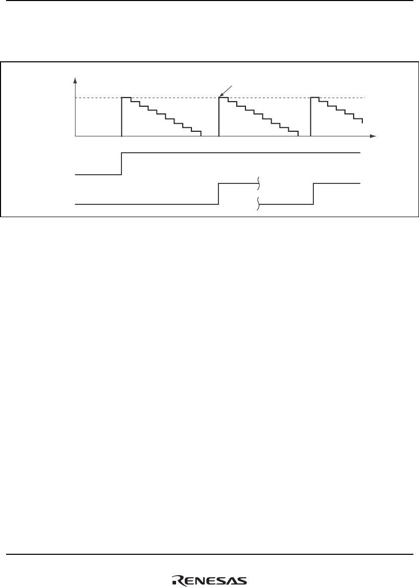
18. Timer Unit (TMU)
Rev.1.00 Jan. 10, 2008 Page 811 of 1658
REJ09B0261-0100
(2) Auto-Reload Count Operation
Figure 18.3 shows the TCNT auto-reload operation.
TCNT value
TCOR
H'0000 0000
STR0 to STR5
UNF
TCOR value is set in TCNT
on underflow
Time
Figure 18.3 TCNT Auto-Reload Operation
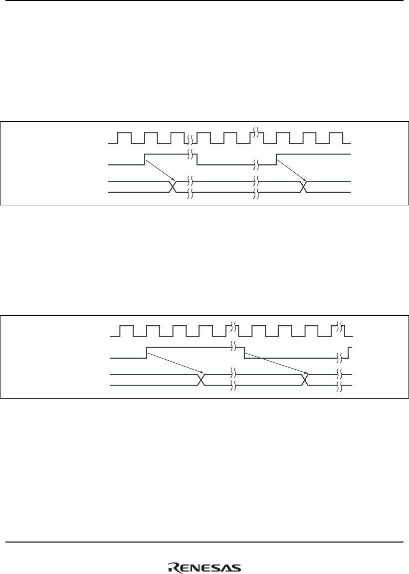
18. Timer Unit (TMU)
Rev.1.00 Jan. 10, 2008 Page 812 of 1658
REJ09B0261-0100
(3) TCNT Count Timing
• Operating on internal clock
Any of five internal count clocks (Pck/4, Pck/16, Pck/64, Pck/256, or Pck/1024) scaled from
the peripheral clock can be selected as the count clock by means of the TPSC2 to TPSC0 bits
in TCR.
Figure 18.4 shows the timing in this case.
Internal clock
Pck
TCNT N + 1 N N – 1
Figure 18.4 Count Timing when Operating on Internal Clock
• Operating on external clock
In channels 0, 1, and 2, the external clock input pin (TCLK) input can be selected as the timer
clock by means of the TPSC2 to TPSC0 bits in TCR. The detected edge (rising, falling, or both
edges) can be selected with the CKEG1 and CKEG0 bits in TCR.
Figure 18.5 shows the timing for both-edge detection.
External clock
input pin (TCLK)
Pck
TCNT N + 1 N N – 1
Figure 18.5 Count Timing when Operating on External Clock Input
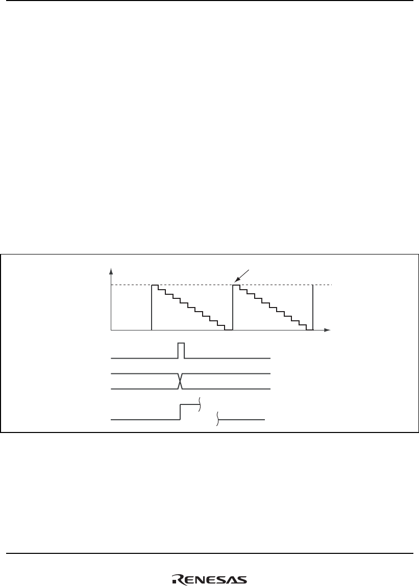
18. Timer Unit (TMU)
Rev.1.00 Jan. 10, 2008 Page 813 of 1658
REJ09B0261-0100
18.4.2 Input Capture Function
Channel 2 has an input capture function.
The procedure for using the input capture function is as follows:
1. Use bits TPSC2 to TPSC0 in TCR2 to set an internal clock as the timer operating clock.
2. Use bits IPCE1 and IPCE0 in TCR2 to specify use of the input capture function, and whether
interrupts are to be generated when this function is used.
3. Use bits CKEG1 and CKEG0 in TCR2 to specify whether the rising or falling edge of the
TCLK pin is to be used to set the TCNT value in TCPR2.
When input capture occurs, the TCNT2 value is set in TCPR2 only when the ICPF bit in TCR2 is
0. A new DMAC transfer request is not generated until processing of the previous request is
finished.
Figure 18.7 shows the operation timing when the input capture function is used (with TCLK rising
edge detection).
TCOR2
H'0000 0000
TCLK
TCPR2
TICPI2
TCNT2 value TCPR2 value is set in TCNT2
on underflow
TCNT2 value is set
Time
Figure 18.6 Operation Timing when Using Input Capture Function

18. Timer Unit (TMU)
Rev.1.00 Jan. 10, 2008 Page 814 of 1658
REJ09B0261-0100
18.5 Interrupts
There are seven TMU interrupt sources: underflow interrupts and the input capture interrupt when
the input capture function is used. Underflow interrupts are generated on each of the channels, and
input capture interrupts on channel 2 only.
An underflow interrupt request is generated (for each channel) when both the UNF bit and the
interrupt enable bit (UNIE) for that channel are set to 1.
When the input capture function is used and an input capture request is generated, an interrupt is
requested if the ICPF bit in TCR2 is 1 and the input capture control bits (ICPE1 and ICPE0) in
TCR2 are both set to 11.
The TMU interrupt sources are summarized in table 18.4.
Table 18.4 TMU Interrupt Sources
Channel Interrupt Source Description
0 TUNI0 Underflow interrupt 0
1 TUNI1 Underflow interrupt 1
2 TUNI2 Underflow interrupt 2
TICPI2 Input capture interrupt 2
3 TUNI3 Underflow interrupt 3
4 TUNI4 Underflow interrupt 4
5 TUNI5 Underflow interrupt 5

18. Timer Unit (TMU)
Rev.1.00 Jan. 10, 2008 Page 815 of 1658
REJ09B0261-0100
18.6 Usage Notes
18.6.1 Register Writes
When writing to a TMU register, timer count operation must be stopped by clearing the start bit
(STR5 to STR0) for the relevant channel in TSTR.
Note that TSTR can be written to, and the UNF and ICPF bits in TCR can be cleared while the
count is in progress. When the flags (UNF and ICPF) are cleared while the count is in progress,
make sure not to change the values of bits other than those being cleared.
18.6.2 Reading from TCNT
Reading from TCNT is performed synchronously with the timer count operation. Note that when
the timer count operation is performed simultaneously with reading from a register, the
synchronous processing causes the TCNT value before the count-down operation to be read as the
TCNT value.
18.6.3 External Clock Frequency
Ensure that the external clock (TCLK) input frequency for channels 0, 1 and 2 does not exceed
Pck/4.

18. Timer Unit (TMU)
Rev.1.00 Jan. 10, 2008 Page 816 of 1658
REJ09B0261-0100

19. Display Unit (DU)
Rev.1.00 Jan. 10, 2008 Page 817 of 1658
REJ09B0261-0100
Section 19 Display Unit (DU)
19.1 Features
The display unit (DU) has the following features.
Plane: The display surfaces normally called the foreground, background, and cursor, are called
planes in this section. Parameters for each plane can be set independently through the settings of
an internal register. The internal register settings can also be used to set the display priority order.
Combined display of up to six planes is possible (however, the plane size is 480 × 234), when the
plane size is WVGA (854 × 480), up to four planes can be combined, when the plane size is
SVGA: 800 × 600, up to three planes can be combined.
• Display size
• Display position
• Display data format (8 bits/pixel, 16 bits/pixel, ARGB (1555), YC)
• Plane superpositioning
• Scrolling
• Wrap-around
• Blinking
• Buffer control
The internal register settings can be used to select two different control modes.
• Manual display change mode (double buffer)
• Auto display change mode (double buffer)
Synchronization Method: Internal register settings can be used to select any of three
synchronization modes for the display output timing.
• Master mode (internal sync mode)
• TV sync mode (external sync mode)
• Sync method switching mode

19. Display Unit (DU)
Rev.1.00 Jan. 10, 2008 Page 818 of 1658
REJ09B0261-0100
CRT Scan Mode (CRT Scan Method): Internal register settings can be used to select from
among three scan modes.
• Non-interlaced mode
• Interlaced sync mode
• Interlaced sync & video mode
YC→RGB Colorspace Conversion Functions: Image data stored in YC format can be converted
into the RGB colorspace and displayed in a window.
(However, when multiple planes are specified for YC → RGB conversion, the YC → RGB
conversion can be performed only for pixels in the uppermost plane.)
Color Palette: Four internal color palette planes are provided, capable of simultaneously
displaying 256 colors out of a possible 260,000 colors. When 8 bits/pixel data is selected in the
plane display format, one among the four planes can be selected.
Eight-bit blend ratios are provided for every 256 colors.
Register Access Control: Internal control registers are provided, and register access is possible
via the peripheral bus interface. The access size is fixed at 32 bits.
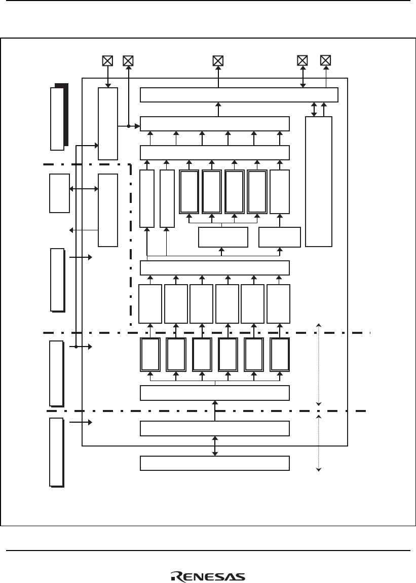
19. Display Unit (DU)
Rev.1.00 Jan. 10, 2008 Page 819 of 1658
REJ09B0261-0100
Figure 19.1 shows a block diagram of the display unit (DU).
Pin control (output timing adjustment)
Display data format selection
Priority contention
determination
16 bit/pixel
(no conversion)
YC to RGB
conversion
Display timing generation
Color palette
contention
determination
YC conversion
contention
determination
Plane rearrangement by priority
1 pixel division
Transparent
color
determination
1 pixel division
Transparent
color
determination
1 pixel division
Transparent
color
determination
1 pixel division
Transparent
color
determination
1 pixel division
Transparent
color
determination
1 pixel division
Transparent
color
determination
Endian conversion
SHwy packet router
Dot clock generation
(frequency division circuit)
Superposition (α blending, EOR operation)
Peripheral bus interface
Peripheral
bus
SHwy interface
irq
Dot clock area
Peripheral clock area
128-bit bus
SHck
64-bit bus
DU clock areaSHwy clock area
DUck
Pck
Color palette 2
(26b x 256w)
Color palette 3
(26b x 256w)
Color palette 4
(26b x 256w)
Color palette 1
(26b x 256w)
DCLKIN DCLKOUT DR5 to DR0
DG5 to DG0
DB5 to DB0
HSYNC
VSYNC
ODDF
DISP
CDE
Buffer-1
(128B x 3)
Buffer-2
(128B x 3)
Buffer-3
(128B x 3)
Buffer-4
(128B x 3)
Buffer-5
(128B x 3)
Buffer-6
(128B x 3)
Legend:
B: byte
b: bit
w: word
Figure 19.1 Block Diagram of the Display Unit (DU)

19. Display Unit (DU)
Rev.1.00 Jan. 10, 2008 Page 820 of 1658
REJ09B0261-0100
19.2 Input/Output Pins
Table 19.1 shows the pin configuration of the display unit (DU).
Table 19.1 Pin Configuration of the Display Unit (DU)
Pin Name Number I/O Function
Signal Name Used
in This Section
DCLKIN 1 I/O Input dot clock DCLKIN
DCLKOUT 1 Output Output dot clock DCLKOUT
HSYNC 1 I/O Composite synchronous output signal
(Initial value)
CSYNC
Horizontal synchronous output/
External horizontal synchronous input
HSYNC (output)/
EXHSYNC (input)
VSYNC 1 I/O Vertical synchronous output/
External vertical synchronous input (Initial
value)
VSYNC (output)/
EXVSYNC (input)
Composite synchronous output signal CSYNC
ODDF 1 I/O Odd/even field (Initial value) ODDF
CLAMP output signal CLAMP
DISP 1 Output Display interval DISP
Composite synchronous output signal CSYNC
DE output signal DE
CDE 1 Output Color detection CDE
DR0 1 Output Digital red 0 Digital RGB
DR1 1 Output Digital red 1
DR2 1 Output Digital red 2
DR3 1 Output Digital red 3
DR4 1 Output Digital red 4
DR5 1 Output Digital red 5
DG0 1 Output Digital green 0
DG1 1 Output Digital green 1
DG2 1 Output Digital green 2
DG3 1 Output Digital green 3
DG4 1 Output Digital green 4

19. Display Unit (DU)
Rev.1.00 Jan. 10, 2008 Page 821 of 1658
REJ09B0261-0100
Pin Name Number I/O Function
Signal Name Used
in This Section
DG5 1 Output Digital green 5
DB0 1 Output Digital blue 0
DB1 1 Output Digital blue 1
DB2 1 Output Digital blue 2
DB3 1 Output Digital blue 3
DB4 1 Output Digital blue 4
DB5 1 Output Digital blue 5
Note: In this section, unless otherwise noted, "dot clock" refers to the output dot clock.
19.3 Register Descriptions
Register update methods include external update and internal update.
(1) External Update
An "external update" is an update which reflects the address-mapped register settings made by the
CPU after the end of CPU access. Registers related to display control (for example, the display
system control register) and the settings of which are updated through external updates can be
overwritten during the vertical blanking interval without display flicker by using the VBK flag and
FRM flag in the display status register (DSSR) indicating the start position of the vertical blanking
interval.
(2) Internal Update
An "internal update" is an update which reflects the address-mapped register settings with the
internal update timing of the display unit (DU). Hence in the case of a register with an internal
update function, even when the CPU overwrites address-mapped registers related to display
operation without being aware of the display timing, display flicker can be prevented.
An internal update is performed during the interval in which the DRES bit in the display system
control register (DSYSR) is 1 and at the beginning of each frame. The internal update performed
at the beginning of each frame can be disabled using the IUPD bit in DSYSR.
Internal updates are performed on the following bits by setting to 1 the DRES bit in DSYSR:

19. Display Unit (DU)
Rev.1.00 Jan. 10, 2008 Page 822 of 1658
REJ09B0261-0100
• Display mode register (DSMR)
⎯ VSPM bit (VSYNC pin mode)
⎯ ODPM bit (ODPM pin mode)
⎯ ODDF bit (ODDF pin mode)
⎯ DIPM bit (DISP pin mode)
⎯ CSPM bit (HSYNC pin mode)
⎯ DIL bit (polarity reversal bit of the DISP pin)
⎯ VSL bit (polarity reversal bit of the VSYNC pin)
⎯ HSL bit (polarity reversal bit of the HSYNC pin)
• Output signal timing adjustment register (OTAR)
⎯ All bits
The registers for the X and Y start positions for plane n in the interlaced sync & video mode
(PnSPXR, PnSPYR) are also internally updated at the beginning of a field.
Internal updates at the beginning of each frame are performed at the falling edge of VSYNC
output when the sync method of DSYSR is master mode (TVM = 00), or at the falling edge of
EXVSYNC detected in TV sync mode (TVM = 10). In sync switching mode (TVM = 11), internal
updates are not performed, and data is retained.
The address-mapped registers with an internal update function are shown in table 19.2. The initial
settings for these registers should be made during the interval in which the DRES bit in DSYSR is
1. For other important information on the timing of register updates, please refer to the
explanations of each register.

19. Display Unit (DU)
Rev.1.00 Jan. 10, 2008 Page 823 of 1658
REJ09B0261-0100
Table 19.2 Register Configuration
Register Name Abbr. R/W
P4
Address
Area 7
Address Size
Synchronous
Clock
Display control registers
Display system control register DSYSR R/W H'FFF80000 H'1FF80000 32 Pck
Display mode register DSMR R/W H'FFF80004 H'1FF80004 32 Pck
Display status register DSSR R H'FFF80008 H'1FF80008 32 Pck
Display status register clear
register
DSRCR W H'FFF8000C H'1FF8000C 32 Pck
Display interrupt enable register DIER R/W H'FFF80010 H'1FF80010 32 Pck
Color palette control register CPCR R/W H'FFF80014 H'1FF80014 32 Pck
Display plane priority order
register
DPPR R/W H'FFF80018 H'1FF80018 32 Pck
Display extension function
enable register
DEFR R/W H'FFF80020 H'1FF80020 32 Pck
Display timing generation registers
Horizontal display start position
register
HDSR R/W H'FFF80040 H'1FF80040 32 Pck
Horizontal display end position
register
HDER R/W H'FFF80044 H'1FF80044 32 Pck
Vertical display start position
register
VDSR R/W H'FFF80048 H'1FF80048 32 Pck
Vertical display end position
register
VDER R/W H'FFF8004C H'1FF8004C 32 Pck
Horizontal scan period register HCR R/W H'FFF80050 H'1FF80050 32 Pck
Horizontal synchronous pulse
width register
HSWR R/W H'FFF80054 H'1FF80054 32 Pck
Vertical scan period register VCR R/W H'FFF80058 H'1FF80058 32 Pck
Vertical synchronous position
register
VSPR R/W H'FFF8005C H'1FF8005C 32 Pck
Equivalent pulse width register EQWR R/W H'FFF80060 H'1FF80060 32 Pck
Separation width register SPWR R/W H'FFF80064 H'1FF80064 32 Pck
CLAMP signal start position
register
CLAMPSR R/W H'FFF80070 H'1FF80070 32 Pck
CLAMP signal width register CLAMPWR R/W H'FFF80074 H'1FF80074 32 Pck

19. Display Unit (DU)
Rev.1.00 Jan. 10, 2008 Page 824 of 1658
REJ09B0261-0100
Register Name Abbr. R/W
P4
Address
Area 7
Address Size
Synchronous
Clock
DE signal start position register DESR R/W H'FFF80078 H'1FF80078 32 Pck
DE signal width register DEWR R/W H'FFF8007C H'1FF8007C 32 Pck
Display attribute registers
Color palette 1 transparent color
register
CP1TR R/W H'FFF80080 H'1FF80080 32 Pck
Color palette 2 transparent color
register
CP2TR R/W H'FFF80084 H'1FF80084 32 Pck
Color palette 3 transparent color
register
CP3TR R/W H'FFF80088 H'1FF80088 32 Pck
Color palette 4 transparent color
register
CP4TR R/W H'FFF8008C H'1FF8008C 32 Pck
Display-off output register DOOR R/W H'FFF80090 H'1FF80090 32 Pck
Color detection register CDER R/W H'FFF80094 H'1FF80094 32 Pck
Base color register BPOR R/W H'FFF80098 H'1FF80098 32 Pck
Raster interrupt offset register RINTOFSR R/W H'FFF8009C H'1FF8009C 32 Pck
Display plane registers
Plane 1 mode register P1MR R/W H'FFF80100 H'1FF80100 32 Pck
Plane 1 memory width register P1MWR R/W H'FFF80104 H'1FF80104 32 Pck
Plane 1 blend ratio register P1ALPHAR R/W H'FFF80108 H'1FF80108 32 Pck
Plane 1 display size X register P1DSXR R/W H'FFF80110 H'1FF80110 32 Pck
Plane 1 display size Y register P1DSYR R/W H'FFF80114 H'1FF80114 32 Pck
Plane 1 display position X
register
P1DPXR R/W H'FFF80118 H'1FF80118 32 Pck
Plane 1 display position Y
register
P1DPYR R/W H'FFF8011C H'1FF8011C 32 Pck
Plane 1 display area start
address 0 register
P1DSA0R R/W H'FFF80120 H'1FF80120 32 Pck
Plane 1 display area start
address 1 register
P1DSA1R R/W H'FFF80124 H'1FF80124 32 Pck
Plane 1 start position X register P1SPXR R/W H'FFF80130 H'1FF80130 32 Pck
Plane 1 start position Y register P1SPYR R/W H'FFF80134 H'1FF80134 32 Pck
Plane 1 wrap-around start
position register
P1WASPR R/W H'FFF80138 H'1FF80138 32 Pck

19. Display Unit (DU)
Rev.1.00 Jan. 10, 2008 Page 825 of 1658
REJ09B0261-0100
Register Name Abbr. R/W
P4
Address
Area 7
Address Size
Synchronous
Clock
Plane 1 wrap-around memory
width register
P1WAMWR R/W H'FFF8013C H'1FF8013C 32 Pck
Plane 1 blinking period register P1BTR R/W H'FFF80140 H'1FF80140 32 Pck
Plane 1 transparent color 1
register
P1TC1R R/W H'FFF80144 H'1FF80144 32 Pck
Plane 1 transparent color 2
register
P1TC2R R/W H'FFF80148 H'1FF80148 32 Pck
Plane 1 memory length register P1MLR R/W H'FFF80150 H'1FF80150 32 Pck
Plane 2 mode register P2MR R/W H'FFF80200 H'1FF80200 32 Pck
Plane 2 memory width register P2MWR R/W H'FFF80204 H'1FF80204 32 Pck
Plane 2 blend ratio register P2ALPHAR R/W H'FFF80208 H'1FF80208 32 Pck
Plane 2 display size X register P2DSXR R/W H'FFF80210 H'1FF80210 32 Pck
Plane 2 display size Y register P2DSYR R/W H'FFF80214 H'1FF80214 32 Pck
Plane 2 display position X
register
P2DPXR R/W H'FFF80218 H'1FF80218 32 Pck
Plane 2 display position Y
register
P2DPYR R/W H'FFF8021C H'1FF8021C 32 Pck
Plane 2 display area start
address 0 register
P2DSA0R R/W H'FFF80220 H'1FF80220 32 Pck
Plane 2 display area start
address 1 register
P2DSA1R R/W H'FFF80224 H'1FF80224 32 Pck
Plane 2 start position X register P2SPXR R/W H'FFF80230 H'1FF80230 32 Pck
Plane 2 start position Y register P2SPYR R/W H'FFF80234 H'1FF80234 32 Pck
Plane 2 wrap-around start
position register
P2WASPR R/W H'FFF80238 H'1FF80238 32 Pck
Plane 2 wrap-around memory
width register
P2WAMWR R/W H'FFF8023C H'1FF8023C 32 Pck
Plane 2 blinking period register P2BTR R/W H'FFF80240 H'1FF80240 32 Pck
Plane 2 transparent color 1
register
P2TC1R R/W H'FFF80244 H'1FF80244 32 Pck
Plane 2 transparent color 2
register
P2TC2R R/W H'FFF80248 H'1FF80248 32 Pck
Plane 2 memory length register P2MLR R/W H'FFF80250 H'1FF80250 32 Pck
Plane 3 mode register P3MR R/W H'FFF80300 H'1FF80300 32 Pck

19. Display Unit (DU)
Rev.1.00 Jan. 10, 2008 Page 826 of 1658
REJ09B0261-0100
Register Name Abbr. R/W
P4
Address
Area 7
Address Size
Synchronous
Clock
Plane 3 memory width register P3MWR R/W H'FFF80304 H'1FF80304 32 Pck
Plane 3 blend ratio register P3ALPHAR R/W H'FFF80308 H'1FF80308 32 Pck
Plane 3 display size X register P3DSXR R/W H'FFF80310 H'1FF80310 32 Pck
Plane 3 display size Y register P3DSYR R/W H'FFF80314 H'1FF80314 32 Pck
Plane 3 display position X
register
P3DPXR R/W H'FFF80318 H'1FF80318 32 Pck
Plane 3 display position Y
register
P3DPYR R/W H'FFF8031C H'1FF8031C 32 Pck
Plane 3 display area start
address 0 register
P3DSA0R R/W H'FFF80320 H'1FF80320 32 Pck
Plane 3 display area start
address 1 register
P3DSA1R R/W H'FFF80324 H'1FF80324 32 Pck
Plane 3 start position X register P3SPXR R/W H'FFF80330 H'1FF80330 32 Pck
Plane 3 start position Y register P3SPYR R/W H'FFF80334 H'1FF80334 32 Pck
Plane 3 wrap-around start
position register
P3WASPR R/W H'FFF80338 H'1FF80338 32 Pck
Plane 3 wrap-around memory
width register
P3WAMWR R/W H'FFF8033C H'1FF8033C 32 Pck
Plane 3 blinking period register P3BTR R/W H'FFF80340 H'1FF80340 32 Pck
Plane 3 transparent color 1
register
P3TC1R R/W H'FFF80344 H'1FF80344 32 Pck
Plane 3 transparent color 2
register
P3TC2R R/W H'FFF80348 H'1FF80348 32 Pck
Plane 3 memory length register P3MLR R/W H'FFF80350 H'1FF80350 32 Pck
Plane 4 mode register P4MR R/W H'FFF80400 H'1FF80400 32 Pck
Plane 4 memory width register P4MWR R/W H'FFF80404 H'1FF80404 32 Pck
Plane 4 blend ratio register P4ALPHAR R/W H'FFF80408 H'1FF80408 32 Pck
Plane 4 display size X register P4DSXR R/W H'FFF80410 H'1FF80410 32 Pck
Plane 4 display size Y register P4DSYR R/W H'FFF80414 H'1FF80414 32 Pck
Plane 4 display position X
register
P4DPXR R/W H'FFF80418 H'1FF80418 32 Pck
Plane 4 display position Y
register
P4DPYR R/W H'FFF8041C H'1FF8041C 32 Pck

19. Display Unit (DU)
Rev.1.00 Jan. 10, 2008 Page 827 of 1658
REJ09B0261-0100
Register Name Abbr. R/W
P4
Address
Area 7
Address Size
Synchronous
Clock
Plane 4 display area start
address 0 register
P4DSA0R R/W H'FFF80420 H'1FF80420 32 Pck
Plane 4 display area start
address 1 register
P4DSA1R R/W H'FFF80424 H'1FF80424 32 Pck
Plane 4 start position X register P4SPXR R/W H'FFF80430 H'1FF80430 32 Pck
Plane 4 start position Y register P4SPYR R/W H'FFF80434 H'1FF80434 32 Pck
Plane 4 wrap-around start
position register
P4WASPR R/W H'FFF80438 H'1FF80438 32 Pck
Plane 4 wrap-around memory
width register
P4WAMWR R/W H'FFF8043C H'1FF8043C 32 Pck
Plane 4 blinking period register P4BTR R/W H'FFF80440 H'1FF80440 32 Pck
Plane 4 transparent color 1
register
P4TC1R R/W H'FFF80444 H'1FF80444 32 Pck
Plane 4 transparent color 2
register
P4TC2R R/W H'FFF80448 H'1FF80448 32 Pck
Plane 4 memory length register P4MLR R/W H'FFF80450 H'1FF80450 32 Pck
Plane 5 mode register P5MR R/W H'FFF80500 H'1FF80500 32 Pck
Plane 5 memory width register P5MWR R/W H'FFF80504 H'1FF80504 32 Pck
Plane 5 blend ratio register P5ALPHAR R/W H'FFF80508 H'1FF80508 32 Pck
Plane 5 display size X register P5DSXR R/W H'FFF80510 H'1FF80510 32 Pck
Plane 5 display size Y register P5DSYR R/W H'FFF80514 H'1FF80514 32 Pck
Plane 5 display position X
register
P5DPXR R/W H'FFF80518 H'1FF80518 32 Pck
Plane 5 display position Y
register
P5DPYR R/W H'FFF8051C H'1FF8051C 32 Pck
Plane 5 display area start
address 0 register
P5DSA0R R/W H'FFF80520 H'1FF80520 32 Pck
Plane 5 display area start
address 1 register
P5DSA1R R/W H'FFF80524 H'1FF80524 32 Pck
Plane 5 start position X register P5SPXR R/W H'FFF80530 H'1FF80530 32 Pck
Plane 5 start position Y register P5SPYR R/W H'FFF80534 H'1FF80534 32 Pck
Plane 5 wrap-around start
position register
P5WASPR R/W H'FFF80538 H'1FF80538 32 Pck

19. Display Unit (DU)
Rev.1.00 Jan. 10, 2008 Page 828 of 1658
REJ09B0261-0100
Register Name Abbr. R/W
P4
Address
Area 7
Address Size
Synchronous
Clock
Plane 5 wrap-around memory
width register
P5WAMWR R/W H'FFF8053C H'1FF8053C 32 Pck
Plane 5 blinking period register P5BTR R/W H'FFF80540 H'1FF80540 32 Pck
Plane 5 transparent color 1
register
P5TC1R R/W H'FFF80544 H'1FF80544 32 Pck
Plane 5 transparent color 2
register
P5TC2R R/W H'FFF80548 H'1FF80548 32 Pck
Plane 5 memory length register P5MLR R/W H'FFF80550 H'1FF80550 32 Pck
Plane 6 mode register P6MR R/W H'FFF80600 H'1FF80600 32 Pck
Plane 6 memory width register P6MWR R/W H'FFF80604 H'1FF80604 32 Pck
Plane 6 blend ratio register P6ALPHAR R/W H'FFF80608 H'1FF80608 32 Pck
Plane 6 display size X register P6DSXR R/W H'FFF80610 H'1FF80610 32 Pck
Plane 6 display size Y register P6DSYR R/W H'FFF80614 H'1FF80614 32 Pck
Plane 6 display position X
register
P6DPXR R/W H'FFF80618 H'1FF80618 32 Pck
Plane 6 display position Y
register
P6DPYR R/W H'FFF8061C H'1FF8061C 32 Pck
Plane 6 display area start
address 0 register
P6DSA0R R/W H'FFF80620 H'1FF80620 32 Pck
Plane 6 display area start
address 1 register
P6DSA1R R/W H'FFF80624 H'1FF80624 32 Pck
Plane 6 start position X register P6SPXR R/W H'FFF80630 H'1FF80630 32 Pck
Plane 6 start position Y register P6SPYR R/W H'FFF80634 H'1FF80634 32 Pck
Plane 6 wrap-around start
position register
P6WASPR R/W H'FFF80638 H'1FF80638 32 Pck
Plane 6 wrap-around memory
width register
P6WAMWR R/W H'FFF8063C H'1FF8063C 32 Pck
Plane 6 blinking period register P6BTR R/W H'FFF80640 H'1FF80640 32 Pck
Plane 6 transparent color 1
register
P6TC1R R/W H'FFF80644 H'1FF80644 32 Pck
Plane 6 transparent color 2
register
P6TC2R R/W H'FFF80648 H'1FF80648 32 Pck
Plane 6 memory length register P6MLR R/W H'FFF80650 H'1FF80650 32 Pck

19. Display Unit (DU)
Rev.1.00 Jan. 10, 2008 Page 829 of 1658
REJ09B0261-0100
Register Name Abbr. R/W
P4
Address
Area 7
Address Size
Synchronous
Clock
Color palette registers
Color palette 1 register 000 CP1_000R R/W H'FFF81000 H'1FF81000 32 Pck
⎯
Color palette 1 register 255 CP1_255R R/W H'FFF813FC H'1FF813FC 32 Pck
Color palette 2 register 000 CP2_000R R/W H'FFF82000 H'1FF82000 32 Pck
⎯
Color palette 2 register 255 CP2_255R R/W H'FFF823FC H'1FF823FC 32 Pck
Color palette 3 register 000 CP3_000R R/W H'FFF83000 H'1FF83000 32 Pck
⎯
Color palette 3 register 255 CP3_255R R/W H'FFF833FC H'1FF833FC 32 Pck
Color palette 4 register 000 CP4_000R R/W H'FFF84000 H'1FF84000 32 Pck
⎯
Color palette 4 register 255 CP4_255R R/W H'FFF843FC H'1FF843FC 32 Pck
External synchronization control register
External synchronization control
register
ESCR R/W H'FFF90000 H'1FF90000 32 Pck
Output signal timing adjustment
register
OTAR R/W H'FFF90004 H'1FF90004 32 Pck

19. Display Unit (DU)
Rev.1.00 Jan. 10, 2008 Page 830 of 1658
REJ09B0261-0100
Table 19.3 Status of Registers in Each Processing Mode
Register Name Abbr.
Power-On
Reset by
PRESET
Pin/ WDT/
H-UDI
Manual
Reset by
WDT
Sleep by
Sleep
Instruction
Module
Standby
Deep
Sleep
Bits with
Internal Update
Function
Display control registers
Display system
control register
DSYSR H'00000280 Retained Retained Retained Retained DSEC
DEN
Display mode
register
DSMR H'00000000 Retained Retained Retained Retained All bits
except the
following bits
which are
updated by the
DRES bit in the
display system
control register
(DSYSR):
VSPM
ODPM
DIPM
CSPM
DIL
VSL
HSL
Display status
register
DSSR H'30000000 Retained Retained Retained Retained None
Display status
register clear
register
DSRCR Undefined Retained Retained Retained Retained None
Display interrupt
enable register
DIER H'00000000 Retained Retained Retained Retained None
Color palette
control register
CPCR H'00000000 Retained Retained Retained Retained All bits
Display plane
priority order
register
DPPR H'00543210 Retained Retained Retained Retained All bits
Display extension
function enable
register
DEFR H'00000000 Retained Retained Retained Retained None

19. Display Unit (DU)
Rev.1.00 Jan. 10, 2008 Page 831 of 1658
REJ09B0261-0100
Register Name Abbr.
Power-On
Reset by
PRESET
Pin/ WDT/
H-UDI
Manual
Reset by
WDT
Sleep by
Sleep
Instruction
Module
Standby
Deep
Sleep
Bits with
Internal Update
Function
Display timing generation registers
Horizontal display
start position
register
HDSR Undefined Retained Retained Retained Retained All bits
Horizontal display
end position
register
HDER Undefined Retained Retained Retained Retained All bits
Vertical display
start position
register
VDSR Undefined Retained Retained Retained Retained All bits
Vertical display
end position
register
VDER Undefined Retained Retained Retained Retained All bits
Horizontal scan
period register
HCR Undefined Retained Retained Retained Retained All bits
Horizontal
synchronous pulse
width register
HSWR Undefined Retained Retained Retained Retained All bits
Vertical scan
period register
VCR Undefined Retained Retained Retained Retained All bits
Vertical
synchronous
position register
VSPR Undefined Retained Retained Retained Retained All bits
Equivalent pulse
width register
EQWR Undefined Retained Retained Retained Retained All bits
Separation width
register
SPWR Undefined Retained Retained Retained Retained All bits
CLAMP signal start
position register
CLAMPSR Undefined Retained Retained Retained Retained All bits
CLAMP signal
width register
CLAMPWR Undefined Retained Retained Retained Retained All bits
DE signal start
position register
DESR Undefined Retained Retained Retained Retained All bits
DE signal width
register
DEWR Undefined Retained Retained Retained Retained All bits

19. Display Unit (DU)
Rev.1.00 Jan. 10, 2008 Page 832 of 1658
REJ09B0261-0100
Register Name Abbr.
Power-On
Reset by
PRESET
Pin/ WDT/
H-UDI
Manual
Reset by
WDT
Sleep by
Sleep
Instruction
Module
Standby
Deep
Sleep
Bits with
Internal Update
Function
Display attribute registers
Color palette 1
transparent color
register
CP1TR H'00000000 Retained Retained Retained Retained All bits
Color palette 2
transparent color
register
CP2TR H'00000000 Retained Retained Retained Retained All bits
Color palette 3
transparent color
register
CP3TR H'00000000 Retained Retained Retained Retained All bits
Color palette 4
transparent color
register
CP4TR H'00000000 Retained Retained Retained Retained All bits
Display-off output
register
DOOR Undefined Retained Retained Retained Retained All bits
Color detection
register
CDER Undefined Retained Retained Retained Retained All bits
Base color register BPOR Undefined Retained Retained Retained Retained All bits
Raster interrupt
offset register
RINTOFSR Undefined Retained Retained Retained Retained All bits
Display plane registers
Plane 1 mode
register
P1MR H'00000000 Retained Retained Retained Retained All bits
Plane 1 memory
width register
P1MWR Undefined Retained Retained Retained Retained All bits
Plane 1 blend ratio
register
P1ALPHAR Undefined Retained Retained Retained Retained All bits
Plane 1 display
size X register
P1DSXR Undefined Retained Retained Retained Retained All bits
Plane 1 display
size Y register
P1DSYR Undefined Retained Retained Retained Retained All bits
Plane 1 display
position X register
P1DPXR Undefined Retained Retained Retained Retained All bits

19. Display Unit (DU)
Rev.1.00 Jan. 10, 2008 Page 833 of 1658
REJ09B0261-0100
Register Name Abbr.
Power-On
Reset by
PRESET
Pin/ WDT/
H-UDI
Manual
Reset by
WDT
Sleep by
Sleep
Instruction
Module
Standby
Deep
Sleep
Bits with
Internal Update
Function
Plane 1 display
position Y register
P1DPYR Undefined Retained Retained Retained Retained All bits
Plane 1 display
area start address
0 register
P1DSA0R Undefined Retained Retained Retained Retained All bits
Plane 1 display
area start address
1 register
P1DSA1R Undefined Retained Retained Retained Retained All bits
Plane 1 start
position X register
P1SPXR Undefined Retained Retained Retained Retained All bits
Plane 1 start
position Y register
P1SPYR Undefined Retained Retained Retained Retained All bits
Plane 1 wrap-
around start
position register
P1WASPR Undefined Retained Retained Retained Retained All bits
Plane 1 wrap-
around memory
width register
P1WAMWR Undefined Retained Retained Retained Retained All bits
Plane 1 blinking
period register
P1BTR H'00000101 Retained Retained Retained Retained All bits
Plane 1
transparent color 1
register
P1TC1R Undefined Retained Retained Retained Retained All bits
Plane 1
transparent color 2
register
P1TC2R Undefined Retained Retained Retained Retained All bits
Plane 1 memory
length register
P1MLR H'00000000 Retained Retained Retained Retained All bits
Plane 2 mode
register
P2MR H'00000000 Retained Retained Retained Retained All bits
Plane 2 memory
width register
P2MWR Undefined Retained Retained Retained Retained All bits
Plane 2 blend ratio
register
P2ALPHAR Undefined Retained Retained Retained Retained All bits

19. Display Unit (DU)
Rev.1.00 Jan. 10, 2008 Page 834 of 1658
REJ09B0261-0100
Register Name Abbr.
Power-On
Reset by
PRESET
Pin/ WDT/
H-UDI
Manual
Reset by
WDT
Sleep by
Sleep
Instruction
Module
Standby
Deep
Sleep
Bits with
Internal Update
Function
Plane 2 display
size X register
P2DSXR Undefined Retained Retained Retained Retained All bits
Plane 2 display
size Y register
P2DSYR Undefined Retained Retained Retained Retained All bits
Plane 2 display
position X register
P2DPXR Undefined Retained Retained Retained Retained All bits
Plane 2 display
position Y register
P2DPYR Undefined Retained Retained Retained Retained All bits
Plane 2 display
area start address
0 register
P2DSA0R Undefined Retained Retained Retained Retained All bits
Plane 2 display
area start address
1 register
P2DSA1R Undefined Retained Retained Retained Retained All bits
Plane 2 start
position X register
P2SPXR Undefined Retained Retained Retained Retained All bits
Plane 2 start
position Y register
P2SPYR Undefined Retained Retained Retained Retained All bits
Plane 2 wrap-
around start
position register
P2WASPR Undefined Retained Retained Retained Retained All bits
Plane 2 wrap-
around memory
width register
P2WAMWR Undefined Retained Retained Retained Retained All bits
Plane 2 blinking
period register
P2BTR H'00000101 Retained Retained Retained Retained All bits
Plane 2
transparent color 1
register
P2TC1R Undefined Retained Retained Retained Retained All bits
Plane 2
transparent color 2
register
P2TC2R Undefined Retained Retained Retained Retained All bits
Plane 2 memory
length register
P2MLR H'00000000 Retained Retained Retained Retained All bits

19. Display Unit (DU)
Rev.1.00 Jan. 10, 2008 Page 835 of 1658
REJ09B0261-0100
Register Name Abbr.
Power-On
Reset by
PRESET
Pin/ WDT/
H-UDI
Manual
Reset by
WDT
Sleep by
Sleep
Instruction
Module
Standby
Deep
Sleep
Bits with
Internal Update
Function
Plane 3 mode
register
P3MR H'00000000 Retained Retained Retained Retained All bits
Plane 3 memory
width register
P3MWR Undefined Retained Retained Retained Retained All bits
Plane 3 blend ratio
register
P3ALPHAR Undefined Retained Retained Retained Retained All bits
Plane 3 display
size X register
P3DSXR Undefined Retained Retained Retained Retained All bits
Plane 3 display
size Y register
P3DSYR Undefined Retained Retained Retained Retained All bits
Plane 3 display
position X register
P3DPXR Undefined Retained Retained Retained Retained All bits
Plane 3 display
position Y register
P3DPYR Undefined Retained Retained Retained Retained All bits
Plane 3 display
area start address
0 register
P3DSA0R Undefined Retained Retained Retained Retained All bits
Plane 3 display
area start address
1 register
P3DSA1R Undefined Retained Retained Retained Retained All bits
Plane 3 start
position X register
P3SPXR Undefined Retained Retained Retained Retained All bits
Plane 3 start
position Y register
P3SPYR Undefined Retained Retained Retained Retained All bits
Plane 3 wrap-
around start
position register
P3WASPR Undefined Retained Retained Retained Retained All bits
Plane 3 wrap-
around memory
width register
P3WAMWR Undefined Retained Retained Retained Retained All bits
Plane 3 blinking
period register
P3BTR H'00000101 Retained Retained Retained Retained All bits
Plane 3
transparent color 1
register
P3TC1R Undefined Retained Retained Retained Retained All bits

19. Display Unit (DU)
Rev.1.00 Jan. 10, 2008 Page 836 of 1658
REJ09B0261-0100
Register Name Abbr.
Power-On
Reset by
PRESET
Pin/ WDT/
H-UDI
Manual
Reset by
WDT
Sleep by
Sleep
Instruction
Module
Standby
Deep
Sleep
Bits with
Internal Update
Function
Plane 3
transparent color 2
register
P3TC2R Undefined Retained Retained Retained Retained All bits
Plane 3 memory
length register
P3MLR H'00000000 Retained Retained Retained Retained All bits
Plane 4 mode
register
P4MR H'00000000 Retained Retained Retained Retained All bits
Plane 4 memory
width register
P4MWR Undefined Retained Retained Retained Retained All bits
Plane 4 blend ratio
register
P4ALPHAR Undefined Retained Retained Retained Retained All bits
Plane 4 display
size X register
P4DSXR Undefined Retained Retained Retained Retained All bits
Plane 4 display
size Y register
P4DSYR Undefined Retained Retained Retained Retained All bits
Plane 4 display
position X register
P4DPXR Undefined Retained Retained Retained Retained All bits
Plane 4 display
position Y register
P4DPYR Undefined Retained Retained Retained Retained All bits
Plane 4 display
area start address
0 register
P4DSA0R Undefined Retained Retained Retained Retained All bits
Plane 4 display
area start address
1 register
P4DSA1R Undefined Retained Retained Retained Retained All bits
Plane 4 start
position X register
P4SPXR Undefined Retained Retained Retained Retained All bits
Plane 4 start
position Y register
P4SPYR Undefined Retained Retained Retained Retained All bits
Plane 4 wrap-
around start
position register
P4WASPR Undefined Retained Retained Retained Retained All bits
Plane 4 wrap-
around memory
width register
P4WAMWR Undefined Retained Retained Retained Retained All bits

19. Display Unit (DU)
Rev.1.00 Jan. 10, 2008 Page 837 of 1658
REJ09B0261-0100
Register Name Abbr.
Power-On
Reset by
PRESET
Pin/ WDT/
H-UDI
Manual
Reset by
WDT
Sleep by
Sleep
Instruction
Module
Standby
Deep
Sleep
Bits with
Internal Update
Function
Plane 4 blinking
period register
P4BTR H'00000101 Retained Retained Retained Retained All bits
Plane 4
transparent color 1
register
P4TC1R Undefined Retained Retained Retained Retained All bits
Plane 4
transparent color 2
register
P4TC2R Undefined Retained Retained Retained Retained All bits
Plane 4 memory
length register
P4MLR H'00000000 Retained Retained Retained Retained All bits
Plane 5 mode
register
P5MR H'00000000 Retained Retained Retained Retained All bits
Plane 5 memory
width register
P5MWR Undefined Retained Retained Retained Retained All bits
Plane 5 blend ratio
register
P5ALPHAR Undefined Retained Retained Retained Retained All bits
Plane 5 display
size X register
P5DSXR Undefined Retained Retained Retained Retained All bits
Plane 5 display
size Y register
P5DSYR Undefined Retained Retained Retained Retained All bits
Plane 5 display
position X register
P5DPXR Undefined Retained Retained Retained Retained All bits
Plane 5 display
position Y register
P5DPYR Undefined Retained Retained Retained Retained All bits
Plane 5 display
area start address
0 register
P5DSA0R Undefined Retained Retained Retained Retained All bits
Plane 5 display
area start address
1 register
P5DSA1R Undefined Retained Retained Retained Retained All bits
Plane 5 start
position X register
P5SPXR Undefined Retained Retained Retained Retained All bits
Plane 5 start
position Y register
P5SPYR Undefined Retained Retained Retained Retained All bits

19. Display Unit (DU)
Rev.1.00 Jan. 10, 2008 Page 838 of 1658
REJ09B0261-0100
Register Name Abbr.
Power-On
Reset by
PRESET
Pin/ WDT/
H-UDI
Manual
Reset by
WDT
Sleep by
Sleep
Instruction
Module
Standby
Deep
Sleep
Bits with
Internal Update
Function
Plane 5 wrap-
around start
position register
P5WASPR Undefined Retained Retained Retained Retained All bits
Plane 5 wrap-
around memory
width register
P5WAMWR Undefined Retained Retained Retained Retained All bits
Plane 5 blinking
period register
P5BTR H'00000101 Retained Retained Retained Retained All bits
Plane 5
transparent color 1
register
P5TC1R Undefined Retained Retained Retained Retained All bits
Plane 5
transparent color 2
register
P5TC2R Undefined Retained Retained Retained Retained All bits
Plane 5 memory
length register
P5MLR H'00000000 Retained Retained Retained Retained All bits
Plane 6 mode
register
P6MR H'00000000 Retained Retained Retained Retained All bits
Plane 6 memory
width register
P6MWR Undefined Retained Retained Retained Retained All bits
Plane 6 blend ratio
register
P6ALPHAR Undefined Retained Retained Retained Retained All bits
Plane 6 display
size X register
P6DSXR Undefined Retained Retained Retained Retained All bits
Plane 6 display
size Y register
P6DSYR Undefined Retained Retained Retained Retained All bits
Plane 6 display
position X register
P6DPXR Undefined Retained Retained Retained Retained All bits
Plane 6 display
position Y register
P6DPYR Undefined Retained Retained Retained Retained All bits
Plane 6 display
area start address
0 register
P6DSA0R Undefined Retained Retained Retained Retained All bits

19. Display Unit (DU)
Rev.1.00 Jan. 10, 2008 Page 839 of 1658
REJ09B0261-0100
Register Name Abbr.
Power-On
Reset by
PRESET
Pin/ WDT/
H-UDI
Manual
Reset by
WDT
Sleep by
Sleep
Instruction
Module
Standby
Deep
Sleep
Bits with
Internal Update
Function
Plane 6 display
area start address
1 register
P6DSA1R Undefined Retained Retained Retained Retained All bits
Plane 6 start
position X register
P6SPXR Undefined Retained Retained Retained Retained All bits
Plane 6 start
position Y register
P6SPYR Undefined Retained Retained Retained Retained All bits
Plane 6 wrap-
around start
position register
P6WASPR Undefined Retained Retained Retained Retained All bits
Plane 6 wrap-
around memory
width register
P6WAMWR Undefined Retained Retained Retained Retained All bits
Plane 6 blinking
period register
P6BTR H'00000101 Retained Retained Retained Retained All bits
Plane 6
transparent color 1
register
P6TC1R Undefined Retained Retained Retained Retained All bits
Plane 6
transparent color 2
register
P6TC2R Undefined Retained Retained Retained Retained All bits
Plane 6 memory
length register
P6MLR H'00000000 Retained Retained Retained Retained All bits
Color palette registers
Color palette 1
register 000
CP1_000R Undefined Retained Retained Retained Retained All bits
⎯
Color palette 1
register 255
CP1_255R Undefined Retained Retained Retained Retained All bits
Color palette 2
register 000
CP2_000R Undefined Retained Retained Retained Retained All bits
⎯
Color palette 2
register 255
CP2_255R Undefined Retained Retained Retained Retained All bits

19. Display Unit (DU)
Rev.1.00 Jan. 10, 2008 Page 840 of 1658
REJ09B0261-0100
Register Name Abbr.
Power-On
Reset by
PRESET
Pin/ WDT/
H-UDI
Manual
Reset by
WDT
Sleep by
Sleep
Instruction
Module
Standby
Deep
Sleep
Bits with
Internal Update
Function
Color palette 3
register 000
CP3_000R Undefined Retained Retained Retained Retained All bits
⎯
Color palette 3
register 255
CP3_255R Undefined Retained Retained Retained Retained All bits
Color palette 4
register 000
CP4_000R Undefined Retained Retained Retained Retained All bits
⎯
Color palette 4
register 255
CP4_255R Undefined Retained Retained Retained Retained All bits
External synchronization control register
External
synchronization
control register
ESCR H'00000000 Retained Retained Retained Retained None
Output signal
timing adjustment
register
OTAR H'00000000 Retained Retained Retained Retained These bits are
updated by the
DRES bit in
DSYSR.

19. Display Unit (DU)
Rev.1.00 Jan. 10, 2008 Page 841 of 1658
REJ09B0261-0100
19.3.1 Display Unit System Control Register
The display unit system control register (DSYSR) sets the system operation for the display unit
(DU).
R/W:
Internal update:
R/W:
Internal update:
161718192021222324252627282931 30Bit:
Initial value:
R/WRRRR/WRRRRRRRRRRR
O
0000000000000000
IUPD
———
DSEC
—————————— —
RRRRR/WR/WR/WR/WR/WR/WRRRRRR
O
0000000101000000
—
———
SCMTVMDENDRES
————— —
01234567891011121315 14Bit:
Initial value:
Bit Bit Name
Initial
Value R/W
Internal
Update Description
31 to 21 ⎯ All 0 R ⎯ Reserved
These bits are always read as 0. The write value
should always be 0.
20 DSEC 0 R/W Yes Display Data Endian Conversion
For details of data swap, see section 19.4.7,
Endian Conversion.
0: Display data in memory is not byte-data/word-
data swapped
1: Display data in memory is byte-data/word-
data swapped
19 to 17 ⎯ All 0 R ⎯ Reserved
These bits are always read as 0. The write value
should always be 0.

19. Display Unit (DU)
Rev.1.00 Jan. 10, 2008 Page 842 of 1658
REJ09B0261-0100
Bit Bit Name
Initial
Value R/W
Internal
Update Description
16 IUPD 0 R/W Yes Internal Updating Disable
When DRES = 1, internal update is performed
regardless of this bit.
For details of internal update, see (2) Internal
Update in section 19.3, Register Descriptions.
0: Internal update is performed upon each
vertical sync signal (VSYNC) assertion
1: By setting this bit to 1, internal updates can be
prohibited.
When this bit is set to 0, register update is
performed upon the next vertical sync signal
(VSYNC).
15 to 10 ⎯ All 0 R ⎯ Reserved
These bits are always read as 0. The write value
should always be 0.

19. Display Unit (DU)
Rev.1.00 Jan. 10, 2008 Page 843 of 1658
REJ09B0261-0100
Bit Bit Name
Initial
Value R/W
Internal
Update Description
9 DRES 1 R/W None Display Reset
8 DEN 0 R/W Yes Display Enable
00: Starts display synchronization operation.
In the case of a register not yet set,
unexpected operation may occur; hence
DRES should be set to 0 after setting all the
registers in the display unit (DU).
When DEN = 0, the display data is the value
set in the display-off output register (DOOR).
01: Starts display synchronization operation.
In the case of a register not yet set,
unexpected operation may occur; hence
DRES and DEN should be set to 0 and 1
respectively after setting all the registers in
the display unit (DU).
When DEN = 1, the display data is the value
stored in memory from the next frame.
10: Halts display and synchronization operation.
Halts display operation and synchronization
operation. Except for the following bits in
DSSR, register settings are held.
For these settings, operation is as follows.
1. All display data output is 0.
2. The following bits in DSSR are cleared to
0.
⎯ TV sync signal error flag (TVR)
⎯ Frame flag (FRM)
⎯ Vertical blanking flag (VBK)
⎯ Raster interrupt flag (RINT)
⎯ Horizontal blanking flag (HBK)
3. The HSYNC, VSYNC, ODDF pins are input
pins.
However, when the ODPM bit in DSMR is 1, the
ODDF pin output is clamped.
11: Setting prohibited

19. Display Unit (DU)
Rev.1.00 Jan. 10, 2008 Page 844 of 1658
REJ09B0261-0100
Bit Bit Name
Initial
Value R/W
Internal
Update Description
7, 6 TVM 10 R/W None TV Synchronization Mode
00: Master mode
HSYNC, VSYNC, CSYNC are output
01: Synchronization method switching mode
When switching from TV sync mode to
master mode, or from master mode to TV
sync mode, is necessary, the switching
should pass through this mode. In this
mode, operation of the display system is
forcibly halted, and DISP outputs a low level
signal. Clock signal supply to the DCLKIN
pin can also be halted (input disabled)
(within the LSI the level is fixed high).
When a clock signal is supplied to the
DCLKIN pin, the clock is output from the
DCLKOUT pin.
The HSYNC pin is the EXHSYNC input, the
VSYNC pin is the EXVSYNC input, and the
ODDF pin is the ODDF input.
However, when the ODPM bit in DSMR is 1,
the ODDF pin output is clamped.
10: TV synchronization mode
The HSYNC pin is the EXHSYNC input, the
VSYNC pin is the EXVSYNC input, and the
ODDF pin is the ODDF input.
However, when the ODPM bit in DSMR is 1,
the ODDF pin output is clamped.
11: Setting prohibited
5, 4 SCM 00 R/W None Scan Mode
00: Non-interlace mode
01: Setting prohibited
10: Interlace sync mode
11: Interlace sync and video mode
3 to 0 ⎯ All 0 R None Reserved
These bits are always read as 0. The write value
should always be 0.

19. Display Unit (DU)
Rev.1.00 Jan. 10, 2008 Page 845 of 1658
REJ09B0261-0100
19.3.2 Display Mode Register (DSMR)
The display mode register (DSMR) sets the display operation of the display unit.
R/W:
Internal update:
R/W:
Internal update:
161718192021222324252627282931 30Bit:
Initial value:
R/WR/WR/WR/WRRRRR/WR/WR/WR/WR/WRRR
**** *****
0000000000000000
DDISHSLVSLDIL
————
CSPMDIPMODPMVSPM
—— —
RRRRRRR/WR/WR/WRRRR/WR/WR/W R/W
* *** *
0000000000000000
—
—————
CSYODEV
———
CDEDCDEL CDEM
01234567891011121315 14Bit:
Initial value:
Bit Bit Name
Initial
Value R/W
Internal
Update Description
31 to 29 ⎯ All 0 R ⎯ Reserved
These bits are always read as 0. The write value
should always be 0.
28 VSPM 0 R/W * VSYNC Pin Mode
Settings in DSYSR are given priority over
settings in this register.
0: VSYNC signal is output to the VSYNC pin
1: CSYNC signal is output to the VSYNC pin
27 ODPM 0 R/W * ODDF Pin Mode
0: ODDF signal is output to the ODDF pin
1: CLAMP signal is output to the ODDF pin
The ODDF pin is an output pin even when the
TVM bit in DSYSR is set to TV sync mode.
26, 25 DIPM 00 R/W * DISP Pin Mode
00: DISP signal is output to the DISP pin
01: CSYNC signal is output to the DISP pin
10: Setting prohibited
11: DE signal is output to the DISP pin

19. Display Unit (DU)
Rev.1.00 Jan. 10, 2008 Page 846 of 1658
REJ09B0261-0100
Bit Bit Name
Initial
Value R/W
Internal
Update Description
24 CSPM 0 R/W * CSYNC Pin Mode
Settings in DSYSR are given priority over
settings in this register.
0: CSYNC signal is output to the HSYNC pin
1: HSYNC signal is output to the HSYNC pin
23 to 20 ⎯ All 0 R ⎯ Reserved
These bits are always read as 0. The write value
should always be 0.
19 DIL 0 R/W * DISP Polarity Select
0: DISP signal at high level during display
interval
1: DISP signal at low level during display interval
18 VSL 0 R/W * VSYNC Polarity Select
0: VSYNC signal is low-active
1: VSYNC signal is high-active
17 HSL 0 R/W * HSYNC Polarity Select
0: HSYNC signal is low-active
1: HSYNC signal is high-active
16 DDIS 0 R/W * DISP Output Disable
0: DISP signal is output
1: DISP signal is not output (fixed to low level)
15 CDEL 0 R/W * CDE Polarity Select
0: CDE signal is high when output display data
and the color detection register (CDER)
match, and is low when they do not match
1: CDE signal is low when output display data
and CDER match, and is high when they do
not match

19. Display Unit (DU)
Rev.1.00 Jan. 10, 2008 Page 847 of 1658
REJ09B0261-0100
Bit Bit Name
Initial
Value R/W
Internal
Update Description
14, 13 CDEM 00 R/W * CDE Output Mode
00: CDE signal is output without change
01: CDE signal is output without change
10: Low level output outside of display interval
(interval when DISP signal is inactive)
11: High level output outside of display interval
(interval when DISP signal is inactive)
12 CDED 0 R/W * CDE Disable
0: CDE signal is output
1: CDE signal is not output (fixed to low level)
11 to 9 ⎯ All 0 R ⎯ Reserved
These bits are always read as 0. The write value
should always be 0.
8 ODEV 0 R/W * ODD Even Select for ODDF Signal
0: In interlaced display of the same frame, when
the ODDF pin is at low level the first half of
the field is displayed.
1: In interlaced display of the same frame, when
the ODDF pin is at high level the first half of
the field is displayed.

19. Display Unit (DU)
Rev.1.00 Jan. 10, 2008 Page 848 of 1658
REJ09B0261-0100
Bit Bit Name
Initial
Value R/W
Internal
Update Description
7, 6 CSY 00 R/W None CSYNC Mode
For details of CSYNC waveform, refer to section
19.5.2, CSYNC.
00: The relation among VSYNC, HSYNC, and
CSYNC is as follows.
VSYNC HSYNC CSYNC
Low level Low level High level
Low level High level Low level
High level Low level Low level
High level High level High level
01: Setting prohibited
10: For the interval of three raster scans after
the falling edge of VSYNC an equivalent
pulse is output, followed by separation pulse
for three raster scans, then an equivalent
pulse for three raster scans, and for the
interval after this the HSYNC waveform is
output as CSYNC.
11: 1/2 raster scan after the VSYNC falling
edge, an equivalent pulse is output for 2.5
raster scans, then separation pulse for 2.5
raster scans, then an equivalent pulse for
2.5 raster scans, and for the interval after
this the HSYNC waveform is output as
CSYNC.
5 to 0 ⎯ All 0 R ⎯ Reserved
These bits are always read as 0. The write value
should always be 0.
Note: * The bit is updated by setting the DRES bit in DSYSR to 1.

19. Display Unit (DU)
Rev.1.00 Jan. 10, 2008 Page 849 of 1658
REJ09B0261-0100
19.3.3 Display Status Register (DSSR)
The display status register (DSSR) is a register used to read, from outside, the internal state of the
display unit (DU).
R/W:
Internal update:
R/W:
Internal update:
161718192021222324252627282931 30Bit:
Initial value:
RRRRRRRRRRRRRRRR
0000000000001100
DFB1DFB2DFB3DFB4DFB5DFB6
————————— —
RRRRRRRRRRRRRRRR
0000000000000000
—
———————
HBKRINT
—
VBK
——
TVR FRM
01234567891011121315 14Bit:
Initial value:
Bit Bit Name
Initial
Value R/W
Internal
Update Description
31, 30 ⎯ 00 R ⎯ Reserved
These bits are always read as 0. The write value
should always be 0.
29, 28 ⎯ 11 R ⎯ Reserved
These bits are always read as 1. The write value
should always be 1.
27 to 22 ⎯ All 0 R ⎯ Reserved
These bits are always read as 0. The write value
should always be 0.
21 DFB6 0 R None Display Frame Buffer 6 Flag
0: The address indicated by the plane 6 display
area start address 0 register (P6DSA0R) in
plane 6 is being used as the display area start
address
1: The address indicated by the plane 6 display
area start address 1 register (P6DSA1R) in
plane 6 is being used as the display area start
address

19. Display Unit (DU)
Rev.1.00 Jan. 10, 2008 Page 850 of 1658
REJ09B0261-0100
Bit Bit Name
Initial
Value R/W
Internal
Update Description
20 DFB5 0 R None Display Frame Buffer 5 Flag
0: The address indicated by the plane 5 display
area start address 0 register (P5DSA0R) in
plane 5 is being used as the display area start
address
1: The address indicated by the plane 5 display
area start address 1 register (P5DSA1R) in
plane 5 is being used as the display area start
address
19 DFB4 0 R None Display Frame Buffer 4 Flag
0: The address indicated by the plane 4 display
area start address 0 register (P4DSA0R) in
plane 4 is being used as the display area start
address
1: The address indicated by the plane 4 display
area start address 1 register (P4DSA1R) in
plane 4 is being used as the display area start
address
18 DFB3 0 R None Display Frame Buffer 3 Flag
0: The address indicated by the plane 3 display
area start address 0 register (P3DSA0R) in
plane 3 is being used as the display area start
address
1: The address indicated by the plane 3 display
area start address 1 register (P3DSA1R) in
plane 3 is being used as the display area start
address
17 DFB2 0 R None Display Frame Buffer 2 Flag
0: The address indicated by the plane 2 display
area start address 0 register (P2DSA0R) in
plane 2 is being used as the display area start
address
1: The address indicated by the plane 2 display
area start address 1 register (P2DSA1R) in
plane 2 is being used as the display area start
address

19. Display Unit (DU)
Rev.1.00 Jan. 10, 2008 Page 851 of 1658
REJ09B0261-0100
Bit Bit Name
Initial
Value R/W
Internal
Update Description
16 DFB1 0 R None Display Frame Buffer 1 Flag
0: The address indicated by the plane 1 display
area start address 0 register (P1DSA0R) in
plane 1 is being used as the display area start
address
1: The address indicated by the plane 1 display
area start address 0 register (P1DSA1R) in
plane 1 is being used as the display area start
address
15 TVR 0 R None TV Synchronization Error Flag
0: After using the DRES bit in DSYSR or the
TVCL bit in the display status register clear
register (DSRCR) to clear the TVR bit to 0,
indicates that the rising edge of EXVSYNC is
being detected each time within the vertical
period determined by the setting of the
vertical scan period register (VCR).
1: Indicates that the rising edge of EXVSYNC
was not detected within the vertical period
determined by the setting of VCR when in TV
sync mode.
The TVR bit holds its state until cleared to 0
by the DRES bit in DSYSR or by the TVCL bit
in DSRCR.
14 FRM 0 R None Frame Flag
0: After clearing to 0 the FRM bit using either the
DRES bit in DSYSR or the FRCL bit in
DSRCR, in interlaced mode indicates the
interval to the next display end, and in
interlaced sync mode or in interlaced sync &
video mode indicates the interval to the
display end of the next even field.
1: After clearing to 0 the FRM bit using either the
DRES bit in DSYSR or the FRCL bit in
DSRCR, indicates the interval until the next
time the FRM bit is cleared, from the first
vertical blanking interval in non-interlaced
mode, and from the first even field blanking
interval in interlaced sync or in interlaced sync
& video mode. (frame units)

19. Display Unit (DU)
Rev.1.00 Jan. 10, 2008 Page 852 of 1658
REJ09B0261-0100
Bit Bit Name
Initial
Value R/W
Internal
Update Description
13, 12 ⎯ All 0 R ⎯ Reserved
These bits are always read as 0. The write value
should always be 0.
11 VBK 0 R None Vertical Blanking Flag
0: Indicates the interval to the next display end
after clearing to 0 the VBK bit using either the
DRES bit in DSYSR or the VBCL bit in
DSRCR.
1: Indicates the interval, after clearing the VBK
bit using either the DRES bit in DSYSR or the
VBCL bit in DSRCR, from the first vertical
blanking interval until the VBK bit is again
cleared to 0. (field units)
10 ⎯ 0 R ⎯ Reserved
This bit is always read as 0. The write value
should always be 0.
9 RINT 0 R None Raster Interrupt Flag
0: Indicates the interval from the start of the next
display until raster scans set in the raster
interrupt offset register have elapsed, after
clearing to 0 the RINT bit using either the
DRES bit in DSYSR or the RICL bit in
DSRCR.
1: After clearing the RINT bit using either the
DRES bit in DSYSR or the RICL bit in
DSRCR, indicates the interval from the start
of the next display after raster scans set in the
raster interrupt offset register have elapsed
until the bit is again cleared to 0.
8 HBK 0 R None Horizontal Blanking Flag
0: Indicates the interval, after clearing to 0 the
HBK bit using the DRES bit in DSYSR or the
HBCL bit in DSRCR, to the next horizontal
blanking.
1: Indicates the interval, after clearing the HBK
bit using either the DRES bit in DSYSR or the
HBCL bit in DSRCR, from the first horizontal
blanking interval until the HBK bit is again
cleared to 0.
7 to 0 ⎯ All 0 R ⎯ Reserved
These bits are always read as 0. The write value
should always be 0.

19. Display Unit (DU)
Rev.1.00 Jan. 10, 2008 Page 853 of 1658
REJ09B0261-0100
19.3.4 Display Unit Status Register Clear Register (DSRCR)
The display unit status register clear register (DSRCR) is a register which clears the various flags
in DSSR.
R/W:
Internal update:
R/W:
Internal update:
161718192021222324252627282931 30Bit:
Initial value:
RRRRRRRRRRRRRRRR
0000000000000000
——————————————— —
RRRRRRRRWWRWRRWW
00000000——0—00——
—
———————
HBCLRICL
—
VBCL
——
TVCL FRCL
01234567891011121315 14Bit:
Initial value:
Bit Bit Name
Initial
Value R/W
Internal
Update Description
31 to 16 ⎯ All 0 R ⎯ Reserved
These bits are always read as 0. The write value
should always be 0.
15 TVCL Undefined W None TV Synchronous Signal Error Flag Clear
0: The TVR flag in DSSR is not changed.
1: The TVR flag in DSSR is cleared to 0.
14 FRCL Undefined W None Flame Flag Clear
0: The FRM flag in DSSR is not changed.
1: The FRM flag in DSSR is cleared to 0.
13, 12 ⎯ All 0 R ⎯ Reserved
These bits are always read as 0. The write value
should always be 0.
11 VBCL Undefined W None Vertical Blanking Flag Clear
0: The VBK flag in DSSR is not changed.
1: The VBK flag in DSSR is cleared to 0.
10 ⎯ 0 R ⎯ Reserved
This bit is always read as 0. The write value
should always be 0.

19. Display Unit (DU)
Rev.1.00 Jan. 10, 2008 Page 854 of 1658
REJ09B0261-0100
Bit Bit Name
Initial
Value R/W
Internal
Update Description
9 RICL Undefined W None Vertical Blanking Flag Clear
0: The RINT flag in DSSR is not changed.
1: The RINT flag in DSSR is cleared to 0.
8 HBCL Undefined W None Vertical Blanking Flag Clear
0: The HBK flag in DSSR is not changed.
1: The HBK flag in DSSR is cleared to 0.
7 to 0 ⎯ All 0 R ⎯ Reserved
These bits are always read as 0. The write value
should always be 0.
19.3.5 Display Unit Interrupt Enable Register (DIER)
The display unit interrupt enable register (DIER) is a register which enables interrupts to the CPU
the causes of which are internal states of the display unit (DU) reflected in DSSR. When bits are
set in this register, if bits in the same bit positions in DSSR are set, an interrupt is issued to the
CPU.
R/W:
Internal update:
R/W:
Internal update:
161718192021222324252627282931 30Bit:
Initial value:
RRRRRRRRRRRRRRRR
0000000000000000
——————————————— —
RRRRRRRRR/WR/WRR/WRRR/W R/W
0000000000000000
—
———————
HBERIE
—
VBE
——
TVE FRE
01234567891011121315 14Bit:
Initial value:

19. Display Unit (DU)
Rev.1.00 Jan. 10, 2008 Page 855 of 1658
REJ09B0261-0100
Bit Bit Name
Initial
Value R/W
Internal
Update Description
31 to 16 ⎯ All 0 R ⎯ Reserved
These bits are always read as 0. The write value
should always be 0.
15 TVE 0 R/W None TV Synchronous Signal Error Interrupt Enable
0: Disables interrupt by the TVR flag in DSSR
1: Enables interrupt by the TVR flag in DSSR
14 FRE 0 R/W None Flame Flag Interrupt Enable
0: Disables interrupt by the FRM flag in DSSR
1: Enables interrupt by the FRM flag in DSSR
13, 12 ⎯ All 0 R ⎯ Reserved
These bits are always read as 0. The write value
should always be 0.
11 VBE 0 R/W None Vertical Blanking Flag Interrupt Enable
0: Disables interrupt by the VBK flag in DSSR
1: Enables interrupt by the VBK flag in DSSR
10 ⎯ 0 R ⎯ Reserved
This bit is always read as 0. The write value
should always be 0.
9 RIE 0 R/W None Vertical Blanking Flag Interrupt Enable
0: Disables interrupt by the RINT flag in DSSR
1: Enables interrupt by the RINT flag in DSSR
8 HBE 0 R/W None Vertical Blanking Flag Interrupt Enable
0: Disables interrupt by the HBK flag in DSSR
1: Enables interrupt by the HBK flag in DSSR
7 to 0 ⎯ All 0 R ⎯ Reserved
These bits are always read as 0. The write value
should always be 0.

19. Display Unit (DU)
Rev.1.00 Jan. 10, 2008 Page 856 of 1658
REJ09B0261-0100
The following are conditions, based on DSSR and this register, for issuing an interrupt to the CPU
from the display unit (DU).
Conditions for issuing an interrupt = a + b + c + d + e
• a = TVR · TVE
• b = FRM · FRE
• c = VBK · VBE
• d = RINT · RIE
• e = HBK · HBE
Interrupts from the display unit (DU) are reflected by bit 27 of the interrupt source register (not
affected by the mask state) (INT2A0) or by bit 27 of the interrupt source register (affected by the
mask state) (INT2A1) of the interrupt controller (INTC).

19. Display Unit (DU)
Rev.1.00 Jan. 10, 2008 Page 857 of 1658
REJ09B0261-0100
19.3.6 Color Palette Control Register (CPCR)
The color palette control register (CPCR) is a register which enables switching of the color palette.
For information on color palette switching, refer to section 19.4.8, Color Palettes.
R/W:
Internal update:
R/W:
Internal update:
161718192021222324252627282931 30Bit:
Initial value:
R/WR/WR/WR/WRRRRRRRRRRRR
OOOO
0000000000000000
CP1CECP2CECP3CECP4CE
——————————— —
RRRRRRRRRRRRRRRR
0000000000000000
—
—————————————— —
01234567891011121315 14Bit:
Initial value:
Bit Bit Name
Initial
Value R/W
Internal
Update Description
31 to 20 ⎯ All 0 R ⎯ Reserved
These bits are always read as 0. The write value
should always be 0.
19 CP4CE 0 R/W Yes Color Palette 4 Change Enable
0: Switching of color palette 4 is not performed.
1: Switching of color palette 4 is performed.
Switching is performed when the DRES bit in
DSYSR is changed from 1 to 0, or with the
timing of an internal update. This bit can only
be set to 1; an operation to set the bit to 0 is
invalid. After switching of the color palette 4,
the bit is cleared to 0.
When setting to 1 and clearing occur
simultaneously, clearing to 0 takes priority.

19. Display Unit (DU)
Rev.1.00 Jan. 10, 2008 Page 858 of 1658
REJ09B0261-0100
Bit Bit Name
Initial
Value R/W
Internal
Update Description
18 CP3CE 0 R/W Yes Color Palette 3 Change Enable
0: Switching of color palette 3 is not performed.
1: Switching of color palette 3 is performed.
Switching is performed when the DRES bit in
DSYSR is changed from 1 to 0, or with the
timing of an internal update. This bit can only
be set to 1; an operation to set the bit to 0 is
invalid. After switching of the color palette 3,
the bit is cleared to 0.
When setting to 1 and clearing occur
simultaneously, clearing to 0 takes priority.
17 CP2CE 0 R/W Yes Color Palette 2 Change Enable
0: Switching of color palette 2 is not performed.
1: Switching of color palette 2 is performed.
Switching is performed when the DRES bit in
DSYSR is changed from 1 to 0, or with the
timing of an internal update. This bit can only
be set to 1; an operation to set the bit to 0 is
invalid. After switching of the color palette 2,
the bit is cleared to 0.
When setting to 1 and clearing occur
simultaneously, clearing to 0 takes priority.
16 CP1CE 0 R/W Yes Color Palette 1 Change Enable
0: Switching of color palette 1 is not performed.
1: Switching of color palette 1 is performed.
Switching is performed when the DRES bit in
DSYSR is changed from 1 to 0, or with the
timing of an internal update. This bit can only
be set to 1; an operation to set the bit to 0 is
invalid. After switching of the color palette 1,
the bit is cleared to 0.
When setting to 1 and clearing occur
simultaneously, clearing to 0 takes priority.
15 to 0 ⎯ All 0 R ⎯ Reserved
These bits are always read as 0. The write value
should always be 0.

19. Display Unit (DU)
Rev.1.00 Jan. 10, 2008 Page 859 of 1658
REJ09B0261-0100
19.3.7 Display Plane Priority Register (DPPR)
The display plane priority register (DPPR) sets the priority order for combining planes and turns
the display on and off.
R/W:
Internal update:
R/W:
Internal update:
161718192021222324252627282931 30Bit:
Initial value:
R/WR/WR/WR/WR/WR/WR/WR/WRRRRRRRR
OOOOOOOO
0010101000000000
DPS5DPE5DPS6DPE6
——————— —
R/WR/WR/WR/WR/WR/WR/WR/WR/WR/WR/WR/WR/WR/WR/W R/W
OOOOOOOOOOOOOOO O
0000100001001100
DPS1DPE1DPS2DPE2DPS3DPE3DPS4DPE4
01234567891011121315 14Bit:
Initial value:
Bit Bit Name
Initial
Value R/W
Internal
Update Description
31 to 24 ⎯ All 0 R ⎯ Reserved
These bits are always read as 0. The write value
should always be 0.
23 DPE6 0 R/W Yes Display Plane Priority 6 Enable
22 to 20 DPS6 101 R/W Yes Display Plane Priority 6 Select
1000: Selects and displays plane 1 in priority 6
1001: Selects and displays plane 2 in priority 6
1010: Selects and displays plane 3 in priority 6
1011: Selects and displays plane 4 in priority 6
1100: Selects and displays plane 5 in priority 6
1101: Selects and displays plane 6 in priority 6
1110: Setting prohibited
1111: Setting prohibited
0---: Priority 6 is not displayed

19. Display Unit (DU)
Rev.1.00 Jan. 10, 2008 Page 860 of 1658
REJ09B0261-0100
Bit Bit Name
Initial
Value R/W
Internal
Update Description
19 DPE5 0 R/W Yes Display Plane Priority 5 Enable
18 to 16 DPS5 100 R/W Yes Display Plane Priority 5 Select
1000: Selects and displays plane 1 in priority 5
1001: Selects and displays plane 2 in priority 5
1010: Selects and displays plane 3 in priority 5
1011: Selects and displays plane 4 in priority 5
1100: Selects and displays plane 5 in priority 5
1101: Selects and displays plane 6 in priority 5
1110: Setting prohibited
1111: Setting prohibited
0---: Priority 5 is not displayed
15 DPE4 0 R/W Yes Display Plane Priority 4 Enable
14 to 12 DPS4 011 R/W Yes Display Plane Priority 4 Select
1000: Selects and displays plane 1 in priority 4
1001: Selects and displays plane 2 in priority 4
1010: Selects and displays plane 3 in priority 4
1011: Selects and displays plane 4 in priority 4
1100: Selects and displays plane 5 in priority 4
1101: Selects and displays plane 6 in priority 4
1110: Setting prohibited
1111: Setting prohibited
0---: Priority 4 is not displayed

19. Display Unit (DU)
Rev.1.00 Jan. 10, 2008 Page 861 of 1658
REJ09B0261-0100
Bit Bit Name
Initial
Value R/W
Internal
Update Description
11 DPE3 0 R/W Yes Display Plane Priority 3 Enable
10 to 8 DPS3 010 R/W Yes Display Plane Priority 3 Select
1000: Selects and displays plane 1 in priority 3
1001: Selects and displays plane 2 in priority 3
1010: Selects and displays plane 3 in priority 3
1011: Selects and displays plane 4 in priority 3
1100: Selects and displays plane 5 in priority 3
1101: Selects and displays plane 6 in priority 3
1110: Setting prohibited
1111: Setting prohibited
0---: Priority 3 is not displayed
7 DPE2 0 R/W Yes Display Plane Priority 2 Enable
6 to 4 DPS2 001 R/W Yes Display Plane Priority 2 Select
1000: Selects and displays plane 1 in priority 2
1001: Selects and displays plane 2 in priority 2
1010: Selects and displays plane 3 in priority 2
1011: Selects and displays plane 4 in priority 2
1100: Selects and displays plane 5 in priority 2
1101: Selects and displays plane 6 in priority 2
1110: Setting prohibited
1111: Setting prohibited
0---: Priority 2 is not displayed
3 DPE1 0 R/W Yes Display Plane Priority 1 Enable
2 to 0 DPS1 000 R/W Yes Display Plane Priority 1 Select
1000: Selects and displays plane 1 in priority 1
1001: Selects and displays plane 2 in priority 1
1010: Selects and displays plane 3 in priority 1
1011: Selects and displays plane 4 in priority 1
1100: Selects and displays plane 5 in priority 1
1101: Selects and displays plane 6 in priority 1
1110: Setting prohibited
1111: Setting prohibited
0---: Priority 1 is not displayed

19. Display Unit (DU)
Rev.1.00 Jan. 10, 2008 Page 862 of 1658
REJ09B0261-0100
19.3.8 Display Unit Extensional Function Enable Register (DEFR)
The display unit extensional function enable register (DEFR) enables extension functions.
DEFR should be set during display reset (the DRES bit and DEN bit in DSYSR should be set to 1
and to 0 respectively) for external updates. If update is performed during display, the display may
flicker.
R/W:
Internal update:
R/W:
Internal update:
161718192021222324252627282931 30Bit:
Initial value:
RRRRRRRRRRRRRRRR
0000000000000000
——————————————— —
R/WRRRR/WR/WRRRRRRRRRR
0000000000000000
DSAE
———
ABREDCKE
————————— —
01234567891011121315 14Bit:
Initial value:
Bit Bit Name
Initial
Value R/W
Internal
Update Description
31 to 6 ⎯ All 0 R ⎯ Reserved
These bits are always read as undefined. The
write value should always be 0.
5 DCKE 0 R/W None Input Dot Clock Select Enable
0: The DCLKSEL bit and bit 4 of the FRQSEL
bits in the external sync control register
(ESCR) are disabled.
1: The DCLKSEL bit and bit 4 of the FRQSEL
bits in ESCR are enabled.
The following functions can be used.
• The clock from the DCLKIN pin and the DU
clock (DUck) can be selected as the input
dot clock. Selection is performed using the
DCLKSEL bit in ESCR.
• The dot clock frequency division ratio can be
selected in the range 0 to 32. The frequency
division ratio is set using the FRQSEL bits in
ESCR.

19. Display Unit (DU)
Rev.1.00 Jan. 10, 2008 Page 863 of 1658
REJ09B0261-0100
Bit Bit Name
Initial
Value R/W
Internal
Update Description
4 ABRE 0 R/W None Alpha Blend Ratio Enable
0: The 31 to 24 bits in the color palette registers
1 to 4 and the PnBRSL bits in the plane n
blend ratio registers (PnALPHAR) are
disabled.
The alpha blend ratio is set only by the
PnALPHA bits PnALPHAR.
1: The 31 to 24 bits in the color palette registers
1 to 4 and the PnBRSL bits in PnALPHAR are
enabled.
• The following can be selected as the alpha
blend ratio. Selection is performed using the
PnBRSL bits in PnALPHAR.
• PnALPHA bits in PnALPHAR
⎯ The 31 to 24 bits in the color palette
registers 1 to 4
⎯ Alpha plane data (display data)
For the alpha blend ratio, refer to section 19.4.9,
Superpositioning of Planes.
3 to 1 ⎯ All 0 R ⎯ Reserved
These bits are always read as undefined. The
write value should always be 0.
0 DSAE 0 R/W None Display Area Start Address Enable
0: The 28 to 4 bits in the plane n display area
start address 0 and 1 registers (PnDSA0R
and PnDSA1R) are enabled.
The 31 to 29 bits are B'000.
1: The 31 to 4 bits PnDSA0R and PnDSA1R are
enabled.

19. Display Unit (DU)
Rev.1.00 Jan. 10, 2008 Page 864 of 1658
REJ09B0261-0100
19.3.9 Horizontal Display Start Register (HDSR)
The horizontal display start register (HDSR) sets the horizontal display start position. The value is
retained during power-on reset and manual reset.
R/W:
Internal update:
R/W:
Internal update:
161718192021222324252627282931 30Bit:
Initial value:
RRRRRRRRRRRRRRRR
0000000000000000
——————————————— —
R/WR/WR/WR/WR/WR/WR/WR/WR/WRRRRRRR
OOOOOOOOO
—————————0000000
HDS
—————— —
01234567891011121315 14Bit:
Initial value:
Bit Bit Name
Initial
Value R/W
Internal
Update Description
31 to 9 ⎯ All 0 R ⎯ Reserved
These bits are always read as 0. The write value
should always be 0.
8 to 0 HDS Undefined R/W Yes Horizontal Display Start
The horizontal display start position should be
set in dot clock units.

19. Display Unit (DU)
Rev.1.00 Jan. 10, 2008 Page 865 of 1658
REJ09B0261-0100
19.3.10 Horizontal Display End Register (HDER)
The horizontal display end register (HDER) sets the horizontal display end position. The value is
retained during power-on reset and manual reset.
R/W:
Internal update:
R/W:
Internal update:
161718192021222324252627282931 30Bit:
Initial value:
RRRRRRRRRRRRRRRR
0000000000000000
——————————————— —
R/WR/WR/WR/WR/WR/WR/WR/WR/WR/WR/WRRRRR
OOOOOOOOOOO
———————————00000
HDE
———— —
01234567891011121315 14Bit:
Initial value:
Bit Bit Name
Initial
Value R/W
Internal
Update Description
31 to 11 ⎯ All 0 R ⎯ Reserved
These bits are always read as 0. The write value
should always be 0.
10 to 0 HDE Undefined R/W Yes Horizontal Display End
The horizontal display end position should be
set in dot clock units.

19. Display Unit (DU)
Rev.1.00 Jan. 10, 2008 Page 866 of 1658
REJ09B0261-0100
19.3.11 Vertical Display Start Register (VDSR)
The vertical display start register (VDSR) sets the vertical display start position. The value is
retained during power-on reset and manual reset.
R/W:
Internal update:
R/W:
Internal update:
161718192021222324252627282931 30Bit:
Initial value:
RRRRRRRRRRRRRRRR
0000000000000000
——————————————— —
R/WR/WR/WR/WR/WR/WR/WR/WR/WRRRRRRR
OOOOOOOOO
—————————0000000
VDS
—————— —
01234567891011121315 14Bit:
Initial value:
Bit Bit Name
Initial
Value R/W
Internal
Update Description
31 to 9 ⎯ All 0 R ⎯ Reserved
These bits are always read as 0. The write value
should always be 0.
8 to 0 VDS Undefined R/W Yes Vertical Display Start
The vertical display start position should be set
in raster line units.

19. Display Unit (DU)
Rev.1.00 Jan. 10, 2008 Page 867 of 1658
REJ09B0261-0100
19.3.12 Vertical Display End Register (VDER)
The vertical display end register (VDER) sets the vertical display end position. The value is
retained during power-on reset and manual reset.
R/W:
Internal update:
R/W:
Internal update:
161718192021222324252627282931 30Bit:
Initial value:
RRRRRRRRRRRRRRRR
0000000000000000
——————————————— —
R/WR/WR/WR/WR/WR/WR/WR/WR/WR/WRRRRRR
OOOOOOOOOO
——————————000000
VDE
————— —
01234567891011121315 14Bit:
Initial value:
Bit Bit Name
Initial
Value R/W
Internal
Update Description
31 to 10 ⎯ All 0 R ⎯ Reserved
These bits are always read as 0. The write value
should always be 0.
9 to 0 VDE Undefined R/W Yes Vertical Display End
The vertical display end position should be set in
raster line units.

19. Display Unit (DU)
Rev.1.00 Jan. 10, 2008 Page 868 of 1658
REJ09B0261-0100
19.3.13 Horizontal Cycle Register (HCR)
The horizontal cycle register (HCR) sets the horizontal scan cycle.(period). The value is retained
during power-on reset and manual reset.
R/W:
Internal update:
R/W:
Internal update:
161718192021222324252627282931 30Bit:
Initial value:
RRRRRRRRRRRRRRRR
0000000000000000
——————————————— —
R/WR/WR/WR/WR/WR/WR/WR/WR/WR/WR/WRRRRR
OOOOOOOOOOO
———————————00000
HC
———— —
01234567891011121315 14Bit:
Initial value:
Bit Bit Name
Initial
Value R/W
Internal
Update Description
31 to 11 ⎯ All 0 R ⎯ Reserved
These bits are always read as 0. The write value
should always be 0.
10 to 0 HC Undefined R/W Yes Horizontal Cycle
One horizontal scan period, including the
horizontal blanking interval, should be set in dot
clock units.
When in TV sync mode, this register should be
set so that the HSYNC period determined by this
register is the same as or greater than the
EXHSYNC period.

19. Display Unit (DU)
Rev.1.00 Jan. 10, 2008 Page 869 of 1658
REJ09B0261-0100
19.3.14 Horizontal Sync Width Register (HSWR)
The horizontal sync width register (HSWR) sets the low-level pulse width of the horizontal sync
signal. The value is retained during power-on reset and manual reset.
R/W:
Internal update:
R/W:
Internal update:
161718192021222324252627282931 30Bit:
Initial value:
RRRRRRRRRRRRRRRR
0000000000000000
——————————————— —
R/WR/WR/WR/WR/WR/WR/WR/WR/WRRRRRRR
OOOOOOOOO
—————————0000000
HSW
—————— —
01234567891011121315 14Bit:
Initial value:
Bit Bit Name
Initial
Value R/W
Internal
Update Description
31 to 9 ⎯ 0 R ⎯ Reserved
These bits are always read as 0. The write value
should always be 0.
8 to 0 HSW Undefined R/W Yes Horizontal Sync Width
The low-level pulse width of the horizontal sync
signal should be set in dot clock units.

19. Display Unit (DU)
Rev.1.00 Jan. 10, 2008 Page 870 of 1658
REJ09B0261-0100
19.3.15 Vertical Cycle Register (VCR)
The vertical cycle register (VCR) sets the vertical scan interval. The value is retained during
power-on reset and manual reset.
R/W:
Internal update:
R/W:
Internal update:
161718192021222324252627282931 30Bit:
Initial value:
RRRRRRRRRRRRRRRR
0000000000000000
——————————————— —
R/WR/WR/WR/WR/WR/WR/WR/WR/WR/WRRRRRR
OOOOOOOOOO
——————————000000
VC
————— —
01234567891011121315 14Bit:
Initial value:
Bit Bit Name
Initial
Value R/W
Internal
Update Description
31 to 10 ⎯ All 0 R ⎯ Reserved
These bits are always read as 0. The write value
should always be 0.
9 to 0 VC Undefined R/W Yes Vertical Cycle
The vertical scan interval, including the vertical
blanking interval, should be set in raster line
units.
When in TV sync mode, the EXVSYNC rising-
edge detection interval time should be set. If not
detected within the interval, the result is
reflected in the TVR flag in DSSR.

19. Display Unit (DU)
Rev.1.00 Jan. 10, 2008 Page 871 of 1658
REJ09B0261-0100
19.3.16 Vertical Sync Point Register (VSPR)
The vertical sync point register (VSPR) sets the start position of the vertical sync signal in raster
line units. The value is retained during power-on reset and manual reset.
R/W:
Internal update:
R/W:
Internal update:
161718192021222324252627282931 30Bit:
Initial value:
RRRRRRRRRRRRRRRR
0000000000000000
——————————————— —
R/WR/WR/WR/WR/WR/WR/WR/WR/WR/WRRRRRR
OOOOOOOOOO
——————————000000
VSP
————— —
01234567891011121315 14Bit:
Initial value:
Bit Bit Name
Initial
Value R/W
Internal
Update Description
31 to 10 ⎯ All 0 R ⎯ Reserved
These bits are always read as 0. The write value
should always be 0.
9 to 0 VSP Undefined R/W Yes Vertical Sync Point
The start position of the vertical sync signal
should be set in raster line units.
When in TV sync mode, this register should be
set such that the VSYNC falling edge set
position in this register is the same as or later
than the EXVSYNC falling edge.

19. Display Unit (DU)
Rev.1.00 Jan. 10, 2008 Page 872 of 1658
REJ09B0261-0100
19.3.17 Equal Pulse Width Register (EQWR)
The equal pulse width register (EQWR) sets the low-level pulse width of a pulse equivalent to the
CSYNC signal. The value is retained during power-on reset and manual reset.
R/W:
Internal update:
R/W:
Internal update:
161718192021222324252627282931 30Bit:
Initial value:
RRRRRRRRRRRRRRRR
0000000000000000
——————————————— —
R/WR/WR/WR/WR/WR/WR/WRRRRRRRRR
OOOOOOO
———————000000000
EQW
———————— —
01234567891011121315 14Bit:
Initial value:
Bit Bit Name
Initial
Value R/W
Internal
Update Description
31 to 7 ⎯ All 0 R ⎯ Reserved
These bits are always read as 0. The write value
should always be 0.
6 to 0 EQW Undefined R/W Yes Equal Pulse Width
The low-level pulse width of a pulse equivalent
to the CSYNC signal should be set in dot clock
units.
To enable this setting, bit 1 of the CSY bits in
DSMR should be set to 1.

19. Display Unit (DU)
Rev.1.00 Jan. 10, 2008 Page 873 of 1658
REJ09B0261-0100
19.3.18 Separation Width Register (SPWR)
The separation width register (SPWR) sets the low-level pulse width of the separation pulse for
the CSYNC signal. The value is retained during power-on reset and manual reset.
R/W:
Internal update:
R/W:
Internal update:
161718192021222324252627282931 30Bit:
Initial value:
RRRRRRRRRRRRRRRR
0000000000000000
——————————————— —
R/WR/WR/WR/WR/WR/WR/WR/WR/WR/WRRRRRR
OOOOOOOOOO
——————————000000
SPW
————— —
01234567891011121315 14Bit:
Initial value:
Bit Bit Name
Initial
Value R/W
Internal
Update Description
31 to 10 ⎯ All 0 R ⎯ Reserved
These bits are always read as 0. The write value
should always be 0.
9 to 0 SPW Undefined R/W Yes Separation Width
The low-level pulse width of the separation pulse
for the CSYNC signal should be set in dot clock
units.
The value set should be smaller than 1/2 the HC
bits in HCR.
To enable this setting, bit 1 of the CSY bits in
DSMR should be set to 1.

19. Display Unit (DU)
Rev.1.00 Jan. 10, 2008 Page 874 of 1658
REJ09B0261-0100
19.3.19 CLAMP Signal Start Register (CLAMPSR)
The CLAMP signal start register (CLAMPSR) sets the rising edge position of the CLAMP signal.
For timing charts for the CLAMP signal and the DE signal, refer to section 19.5.6, CLAMP Signal
and DE Signal.
The value is retained during power-on reset and manual reset.
R/W:
Internal update:
R/W:
Internal update:
Bit:
Initial value:
Bit:
Initial value:
161718192021222324252627282931 30
RRRRRRRRRRRRRRRR
0000000000000000
——————————————— —
R/WR/WR/WR/WR/WR/WR/WR/WR/WR/WR/WRRRRR
OOOOOOOOOOO
———————————00000
CLAMPS
———— —
01234567891011121315 14
Bit Bit Name
Initial
Value R/W
Internal
Update Description
31 to 11 ⎯ All 0 R ⎯ Reserved
These bits are always read as 0. The write value
should always be 0.
10 to 0 CLAMPS Undefined R/W Yes Clamp Signal Start
The CLAMP signal rising edge position should
be set in dot clock units relative to the falling
edge of the HSYNC signal.
The CLAMP signal rises (setting + 1) cycles
after the falling edge of the HSYNC signal.
Hence the CLAMP signal cannot be made to
rise in the same cycle as the falling edge of the
HSYNC signal.

19. Display Unit (DU)
Rev.1.00 Jan. 10, 2008 Page 875 of 1658
REJ09B0261-0100
19.3.20 CLAMP Signal Width Register (CLAMPWR)
The CLAMP signal width register (CLAMPWR) sets the high-level width of the CLAMP signal.
The value is retained during power-on reset and manual reset.
R/W:
Internal update:
R/W:
Internal update:
Bit:
Initial value:
Bit:
Initial value:
161718192021222324252627282931 30
RRRRRRRRRRRRRRRR
0000000000000000
——————————————— —
R/WR/WR/WR/WR/WR/WR/WR/WR/WR/WR/WRRRRR
OOOOOOOOOOO
———————————00000
CLAMPW
———— —
01234567891011121315 14
Bit Bit Name
Initial
Value R/W
Internal
Update Description
31 to 11 ⎯ All 0 R ⎯ Reserved
These bits are always read as 0. The write value
should always be 0.
10 to 0 CLAMPW Undefined R/W Yes Clamp Signal Width
The high-level width of the CLAMP signal should
be set in dot clock units.
If the HSYNC signal falls while the CLAMP
signal is at high level, the CLAMP signal also
falls.

19. Display Unit (DU)
Rev.1.00 Jan. 10, 2008 Page 876 of 1658
REJ09B0261-0100
19.3.21 DE Signal Start Register (DESR)
The DE signal start register (DESR) sets the rising edge position of the DE signal. The value is
retained during power-on reset and manual reset.
R/W:
Internal update:
R/W:
Internal update:
161718192021222324252627282931 30Bit:
Initial value:
RRRRRRRRRRRRRRRR
0000000000000000
——————————————— —
R/WR/WR/WR/WR/WR/WR/WR/WR/WR/WR/WRRRRR
OOOOOOOOOOO
———————————00000
DES
———— —
01234567891011121315 14Bit:
Initial value:
Bit Bit Name
Initial
Value R/W
Internal
Update Description
31 to 11 ⎯ All 0 R ⎯ Reserved
These bits are always read as 0. The write value
should always be 0.
10 to 0 DES Undefined R/W Yes DE Signal Start
The DE signal rising edge position should be set
in dot clock units relative to the falling edge of
the HSYNC signal.
The DE signal rises (setting + 1) cycles after the
falling edge of the HSYNC signal. Hence the DE
signal cannot be made to rise in the same cycle
as the falling edge of the HSYNC signal.
During the vertical blanking interval the level is
fixed at low level.

19. Display Unit (DU)
Rev.1.00 Jan. 10, 2008 Page 877 of 1658
REJ09B0261-0100
19.3.22 DE Signal Width Register (DEWR)
The DE signal width register (DEWR) sets the high-level width of the DE signal. The value is
retained during power-on reset and manual reset.
R/W:
Internal update:
R/W:
Internal update:
161718192021222324252627282931 30Bit:
Initial value:
RRRRRRRRRRRRRRRR
0000000000000000
——————————————— —
R/WR/WR/WR/WR/WR/WR/WR/WR/WR/WR/WRRRRR
OOOOOOOOOOO
———————————00000
DEW
———— —
01234567891011121315 14Bit:
Initial value:
Bit Bit Name
Initial
Value R/W
Internal
Update Description
31 to 11 ⎯ All 0 R ⎯ Reserved
These bits are always read as 0. The write value
should always be 0.
10 to 0 DEW Undefined R/W Yes DE Signal Width
The high-level width of the DE signal should be
set in dot clock units.
If the HSYNC signal falls while the DE signal is
at high level, the DE signal also falls.

19. Display Unit (DU)
Rev.1.00 Jan. 10, 2008 Page 878 of 1658
REJ09B0261-0100
19.3.23 Color Palette 1 Transparent Color Register (CP1TR)
The color palette 1 transparent color register (CP1TR) specifies the transparent color for color
palette 1.
R/W:
Internal update:
R/W:
Internal update:
161718192021222324252627282931 30Bit:
Initial value:
RRRRRRRRRRRRRRRR
0000000000000000
——————————————— —
R/WR/WR/WR/WR/WR/WR/WR/WR/WR/WR/WR/WR/WR/WR/W R/W
OOOOOOOOOOOOOOO O
0000000000000000
CP1I0
CP1I1CP1I2CP1I3CP1I4CP1I5CP1I6CP1I7CP1I8CP1I9CP1IACP1IBCP1ICCP1IDCP1IF CP1IE
01234567891011121315 14Bit:
Initial value:
Bit Bit Name
Initial
Value R/W
Internal
Update Description
31 to 16 ⎯ All 0 R ⎯ Reserved
These bits are always read as 0. The write value
should always be 0.
15 CP1IF 0 R/W Yes Color Palette 1 Index F
0: The color with index F in color palette 1 is not
set to the transparent color.
1: The color with index F in color palette 1 is set
to the transparent color.
14 CP1IE 0 R/W Yes Color Palette 1 Index E
0: The color with index E in color palette 1 is not
set to the transparent color.
1: The color with index E in color palette 1 is set
to the transparent color.
13 CP1ID 0 R/W Yes Color Palette 1 Index D
0: The color with index D in color palette 1 is not
set to the transparent color.
1: The color with index D in color palette 1 is set
to the transparent color.

19. Display Unit (DU)
Rev.1.00 Jan. 10, 2008 Page 879 of 1658
REJ09B0261-0100
Bit Bit Name
Initial
Value R/W
Internal
Update Description
12 CP1IC 0 R/W Yes Color Palette 1 Index C
0: The color with index C in color palette 1 is not
set to the transparent color.
1: The color with index C in color palette 1 is set
to the transparent color.
11 CP1IB 0 R/W Yes Color Palette 1 Index B
0: The color with index B in color palette 1 is not
set to the transparent color.
1: The color with index B in color palette 1 is set
to the transparent color.
10 CP1IA 0 R/W Yes Color Palette 1 Index A
0: The color with index A in color palette 1 is not
set to the transparent color.
1: The color with index A in color palette 1 is set
to the transparent color.
9 CP1I9 0 R/W Yes Color Palette 1 Index 9
0: The color with index 9 in color palette 1 is not
set to the transparent color.
1: The color with index 9 in color palette 1 is set
to the transparent color.
8 CP1I8 0 R/W Yes Color Palette 1 Index 8
0: The color with index 8 in color palette 1 is not
set to the transparent color.
1: The color with index 8 in color palette 1 is set
to the transparent color.
7 CP1I7 0 R/W Yes Color Palette 1 Index 7
0: The color with index 7 in color palette 1 is not
set to the transparent color.
1: The color with index 7 in color palette 1 is set
to the transparent color.
6 CP1I6 0 R/W Yes Color Palette 1 Index 6
0: The color with index 6 in color palette 1 is not
set to the transparent color.
1: The color with index 6 in color palette 1 is set
to the transparent color.

19. Display Unit (DU)
Rev.1.00 Jan. 10, 2008 Page 880 of 1658
REJ09B0261-0100
Bit Bit Name
Initial
Value R/W
Internal
Update Description
5 CP1I5 0 R/W Yes Color Palette 1 Index 5
0: The color with index 5 in color palette 1 is not
set to the transparent color.
1: The color with index 5 in color palette 1 is set
to the transparent color.
4 CP1I4 0 R/W Yes Color Palette 1 Index 4
0: The color with index 4 in color palette 1 is not
set to the transparent color.
1: The color with index 4 in color palette 1 is set
to the transparent color.
3 CP1I3 0 R/W Yes Color Palette 1 Index 3
0: The color with index 3 in color palette 1 is not
set to the transparent color.
1: The color with index 3 in color palette 1 is set
to the transparent color.
2 CP1I2 0 R/W Yes Color Palette 1 Index 2
0: The color with index 2 in color palette 1 is not
set to the transparent color.
1: The color with index 2 in color palette 1 is set
to the transparent color.
1 CP1I1 0 R/W Yes Color Palette 1 Index 1
0: The color with index 1 in color palette 1 is not
set to the transparent color.
1: The color with index 1 in color palette 1 is set
to the transparent color.
0 CP1I0 0 R/W Yes Color Palette 1 Index 0
0: The color with index 0 in color palette 1 is not
set to the transparent color.
1: The color with index 0 in color palette 1 is set
to the transparent color.

19. Display Unit (DU)
Rev.1.00 Jan. 10, 2008 Page 881 of 1658
REJ09B0261-0100
19.3.24 Color Palette 2 Transparent Color Register (CP2TR)
The color palette 2 transparent color register (CP2TR) specifies the transparent color of color
palette 2.
R/W:
Internal update:
R/W:
Internal update:
161718192021222324252627282931 30Bit:
Initial value:
RRRRRRRRRRRRRRRR
0000000000000000
——————————————— —
R/WR/WR/WR/WR/WR/WR/WR/WR/WR/WR/WR/WR/WR/WR/W R/W
OOOOOOOOOOOOOOO O
0000000000000000
CP2I0
CP2I1CP2I2CP2I3CP2I4CP2I5CP2I6CP2I7CP2I8CP2I9CP2IACP2IBCP2ICCP2IDCP2IF CP2IE
01234567891011121315 14Bit:
Initial value:
Bit Bit Name
Initial
Value R/W
Internal
Update Description
31 to 16 ⎯ All 0 R ⎯ Reserved
These bits are always read as 0. The write value
should always be 0.
15 CP2IF 0 R/W Yes Color Palette 2 Index F
0: The color with index F in color palette 2 is not
set to the transparent color.
1: The color with index F in color palette 2 is set
to the transparent color.
14 CP2IE 0 R/W Yes Color Palette 2 Index E
0: The color with index E in color palette 2 is not
set to the transparent color.
1: The color with index E in color palette 2 is set
to the transparent color.
13 CP2ID 0 R/W Yes Color Palette 2 Index D
0: The color with index D in color palette 2 is not
set to the transparent color.
1: The color with index D in color palette 2 is set
to the transparent color.

19. Display Unit (DU)
Rev.1.00 Jan. 10, 2008 Page 882 of 1658
REJ09B0261-0100
Bit Bit Name
Initial
Value R/W
Internal
Update Description
12 CP2IC 0 R/W Yes Color Palette 2 Index C
0: The color with index C in color palette 2 is not
set to the transparent color.
1: The color with index C in color palette 2 is set
to the transparent color.
11 CP2IB 0 R/W Yes Color Palette 2 Index B
0: The color with index B in color palette 2 is not
set to the transparent color.
1: The color with index B in color palette 2 is set
to the transparent color.
10 CP2IA 0 R/W Yes Color Palette 2 Index A
0: The color with index A in color palette 2 is not
set to the transparent color.
1: The color with index A in color palette 2 is set
to the transparent color.
9 CP2I9 0 R/W Yes Color Palette 2 Index 9
0: The color with index 9 in color palette 2 is not
set to the transparent color.
1: The color with index 9 in color palette 2 is set
to the transparent color.
8 CP2I8 0 R/W Yes Color Palette 2 Index 8
0: The color with index 8 in color palette 2 is not
set to the transparent color.
1: The color with index 8 in color palette 2 is set
to the transparent color.
7 CP2I7 0 R/W Yes Color Palette 2 Index 7
0: The color with index 7 in color palette 2 is not
set to the transparent color.
1: The color with index 7 in color palette 2 is set
to the transparent color.
6 CP2I6 0 R/W Yes Color Palette 2 Index 6
0: The color with index 6 in color palette 2 is not
set to the transparent color.
1: The color with index 6 in color palette 2 is set
to the transparent color.

19. Display Unit (DU)
Rev.1.00 Jan. 10, 2008 Page 883 of 1658
REJ09B0261-0100
Bit Bit Name
Initial
Value R/W
Internal
Update Description
5 CP2I5 0 R/W Yes Color Palette 2 Index 5
0: The color with index 5 in color palette 2 is not
set to the transparent color.
1: The color with index 5 in color palette 2 is set
to the transparent color.
4 CP2I4 0 R/W Yes Color Palette 2 Index 4
0: The color with index 4 in color palette 2 is not
set to the transparent color.
1: The color with index 4 in color palette 2 is set
to the transparent color.
3 CP2I3 0 R/W Yes Color Palette 2 Index 3
0: The color with index 3 in color palette 2 is not
set to the transparent color.
1: The color with index 3 in color palette 2 is set
to the transparent color.
2 CP2I2 0 R/W Yes Color Palette 2 Index 2
0: The color with index 2 in color palette 2 is not
set to the transparent color.
1: The color with index 2 in color palette 2 is set
to the transparent color.
1 CP2I1 0 R/W Yes Color Palette 2 Index 1
0: The color with index 1 in color palette 2 is not
set to the transparent color.
1: The color with index 1 in color palette 2 is set
to the transparent color.
0 CP2I0 0 R/W Yes Color Palette 2 Index 0
0: The color with index 0 in color palette 2 is not
set to the transparent color.
1: The color with index 0 in color palette 2 is set
to the transparent color.

19. Display Unit (DU)
Rev.1.00 Jan. 10, 2008 Page 884 of 1658
REJ09B0261-0100
19.3.25 Color Palette 3 Transparent Color Register (CP3TR)
The color palette 3 transparent color register (CP3TR) specifies the transparent color of color
palette 3.
R/W:
Internal update:
R/W:
Internal update:
161718192021222324252627282931 30Bit:
Initial value:
RRRRRRRRRRRRRRRR
0000000000000000
——————————————— —
R/WR/WR/WR/WR/WR/WR/WR/WR/WR/WR/WR/WR/WR/WR/W R/W
OOOOOOOOOOOOOOO O
0000000000000000
CP3I0
CP3I1CP3I2CP3I3CP3I4CP3I5CP3I6CP3I7CP3I8CP3I9CP3IACP3IBCP3ICCP3IDCP3IF CP3IE
01234567891011121315 14Bit:
Initial value:
Bit Bit Name
Initial
Value R/W
Internal
Update Description
31 to 16 ⎯ All 0 R ⎯ Reserved
These bits are always read as 0. The write value
should always be 0.
15 CP3IF 0 R/W Yes Color Palette 3 Index F
0: The color with index F in color palette 3 is not
set to the transparent color.
1: The color with index F in color palette 3 is set
to the transparent color.
14 CP3IE 0 R/W Yes Color Palette 3 Index E
0: The color with index E in color palette 3 is not
set to the transparent color.
1: The color with index E in color palette 3 is set
to the transparent color.
13 CP3ID 0 R/W Yes Color Palette 3 Index D
0: The color with index D in color palette 3 is not
set to the transparent color.
1: The color with index D in color palette 3 is set
to the transparent color.

19. Display Unit (DU)
Rev.1.00 Jan. 10, 2008 Page 885 of 1658
REJ09B0261-0100
Bit Bit Name
Initial
Value R/W
Internal
Update Description
12 CP3IC 0 R/W Yes Color Palette 3 Index C
0: The color with index C in color palette 3 is not
set to the transparent color.
1: The color with index C in color palette 3 is set
to the transparent color.
11 CP3IB 0 R/W Yes Color Palette 3 Index B
0: The color with index B in color palette 3 is not
set to the transparent color.
1: The color with index B in color palette 3 is set
to the transparent color.
10 CP3IA 0 R/W Yes Color Palette 3 Index A
0: The color with index A in color palette 3 is not
set to the transparent color.
1: The color with index A in color palette 3 is set
to the transparent color.
9 CP3I9 0 R/W Yes Color Palette 3 Index 9
0: The color with index 9 in color palette 3 is not
set to the transparent color.
1: The color with index 9 in color palette 3 is set
to the transparent color.
8 CP3I8 0 R/W Yes Color Palette 3 Index 8
0: The color with index 8 in color palette 3 is not
set to the transparent color.
1: The color with index 8 in color palette 3 is set
to the transparent color.
7 CP3I7 0 R/W Yes Color Palette 3 Index 7
0: The color with index 7 in color palette 3 is not
set to the transparent color.
1: The color with index 7 in color palette 3 is set
to the transparent color.
6 CP3I6 0 R/W Yes Color Palette 3 Index 6
0: The color with index 6 in color palette 3 is not
set to the transparent color.
1: The color with index 6 in color palette 3 is set
to the transparent color.

19. Display Unit (DU)
Rev.1.00 Jan. 10, 2008 Page 886 of 1658
REJ09B0261-0100
Bit Bit Name
Initial
Value R/W
Internal
Update Description
5 CP3I5 0 R/W Yes Color Palette 3 Index 5
0: The color with index 5 in color palette 3 is not
set to the transparent color.
1: The color with index 5 in color palette 3 is set
to the transparent color.
4 CP3I4 0 R/W Yes Color Palette 3 Index 4
0: The color with index 4 in color palette 3 is not
set to the transparent color.
1: The color with index 4 in color palette 3 is set
to the transparent color.
3 CP3I3 0 R/W Yes Color Palette 3 Index 3
0: The color with index 3 in color palette 3 is not
set to the transparent color.
1: The color with index 3 in color palette 3 is set
to the transparent color.
2 CP3I2 0 R/W Yes Color Palette 3 Index 2
0: The color with index 2 in color palette 3 is not
set to the transparent color.
1: The color with index 2 in color palette 3 is set
to the transparent color.
1 CP3I1 0 R/W Yes Color Palette 3 Index 1
0: The color with index 1 in color palette 3 is not
set to the transparent color.
1: The color with index 1 in color palette 3 is set
to the transparent color.
0 CP3I0 0 R/W Yes Color Palette 3 Index 0
0: The color with index 0 in color palette 3 is not
set to the transparent color.
1: The color with index 0 in color palette 3 is set
to the transparent color.

19. Display Unit (DU)
Rev.1.00 Jan. 10, 2008 Page 887 of 1658
REJ09B0261-0100
19.3.26 Color Palette 4 Transparent Color Register (CP4TR)
The color palette 4 transparent color register (CP4TR) specifies the transparent color of color
palette 4.
R/W:
Internal update:
R/W:
Internal update:
161718192021222324252627282931 30Bit:
Initial value:
RRRRRRRRRRRRRRRR
0000000000000000
——————————————— —
R/WR/WR/WR/WR/WR/WR/WR/WR/WR/WR/WR/WR/WR/WR/W R/W
OOOOOOOOOOOOOOO O
0000000000000000
CP4I0
CP4I1CP4I2CP4I3CP4I4CP4I5CP4I6CP4I7CP4I8CP4I9CP4IACP4IBCP4ICCP4IDCP4IF CP4IE
01234567891011121315 14Bit:
Initial value:
Bit Bit Name
Initial
Value R/W
Internal
Update Description
31 to 16 ⎯ All 0 R ⎯ Reserved
These bits are always read as 0. The write value
should always be 0.
15 CP4IF 0 R/W Yes Color Palette 4 Index F
0: The color with index F in color palette 4 is not
set to the transparent color.
1: The color with index F in color palette 4 is set
to the transparent color.
14 CP4IE 0 R/W Yes Color Palette 4 Index E
0: The color with index E in color palette 4 is not
set to the transparent color.
1: The color with index E in color palette 4 is set
to the transparent color.
13 CP4ID 0 R/W Yes Color Palette 4 Index D
0: The color with index D in color palette 4 is not
set to the transparent color.
1: The color with index D in color palette 4 is set
to the transparent color.

19. Display Unit (DU)
Rev.1.00 Jan. 10, 2008 Page 888 of 1658
REJ09B0261-0100
Bit Bit Name
Initial
Value R/W
Internal
Update Description
12 CP4IC 0 R/W Yes Color Palette 4 Index C
0: The color with index C in color palette 4 is not
set to the transparent color.
1: The color with index C in color palette 4 is set
to the transparent color.
11 CP4IB 0 R/W Yes Color Palette 4 Index B
0: The color with index B in color palette 4 is not
set to the transparent color.
1: The color with index B in color palette 4 is set
to the transparent color.
10 CP4IA 0 R/W Yes Color Palette 4 Index A
0: The color with index A in color palette 4 is not
set to the transparent color.
1: The color with index A in color palette 4 is set
to the transparent color.
9 CP4I9 0 R/W Yes Color Palette 4 Index 9
0: The color with index 9 in color palette 4 is not
set to the transparent color.
1: The color with index 9 in color palette 4 is set
to the transparent color.
8 CP4I8 0 R/W Yes Color Palette 4 Index 8
0: The color with index 8 in color palette 4 is not
set to the transparent color.
1: The color with index 8 in color palette 4 is set
to the transparent color.
7 CP4I7 0 R/W Yes Color Palette 4 Index 7
0: The color with index 7 in color palette 4 is not
set to the transparent color.
1: The color with index 7 in color palette 4 is set
to the transparent color.
6 CP4I6 0 R/W Yes Color Palette 4 Index 6
0: The color with index 6 in color palette 4 is not
set to the transparent color.
1: The color with index 6 in color palette 4 is set
to the transparent color.

19. Display Unit (DU)
Rev.1.00 Jan. 10, 2008 Page 889 of 1658
REJ09B0261-0100
Bit Bit Name
Initial
Value R/W
Internal
Update Description
5 CP4I5 0 R/W Yes Color Palette 4 Index 5
0: The color with index 5 in color palette 4 is not
set to the transparent color.
1: The color with index 5 in color palette 4 is set
to the transparent color.
4 CP4I4 0 R/W Yes Color Palette 4 Index 4
0: The color with index 4 in color palette 4 is not
set to the transparent color.
1: The color with index 4 in color palette 4 is set
to the transparent color.
3 CP4I3 0 R/W Yes Color Palette 4 Index 3
0: The color with index 3 in color palette 4 is not
set to the transparent color.
1: The color with index 3 in color palette 4 is set
to the transparent color.
2 CP4I2 0 R/W Yes Color Palette 4 Index 2
0: The color with index 2 in color palette 4 is not
set to the transparent color.
1: The color with index 2 in color palette 4 is set
to the transparent color.
1 CP4I1 0 R/W Yes Color Palette 4 Index 1
0: The color with index 1 in color palette 4 is not
set to the transparent color.
1: The color with index 1 in color palette 4 is set
to the transparent color.
0 CP4I0 0 R/W Yes Color Palette 4 Index 0
0: The color with index 0 in color palette 4 is not
set to the transparent color.
1: The color with index 0 in color palette 4 is set
to the transparent color.

19. Display Unit (DU)
Rev.1.00 Jan. 10, 2008 Page 890 of 1658
REJ09B0261-0100
19.3.27 Display Off Mode Output Register (DOOR)
The display off mode output register (DOOR) sets the display data output when the display is
turned off. The value is retained during power-on reset and manual reset.
R/W:
Internal update:
R/W:
Internal update:
161718192021222324252627282931 30Bit:
Initial value:
RRR/WR/WR/WR/WR/WR/WRRRRRRRR
OOOOOO
00——————00000000
——
DOR
——————— —
RRR/WR/WR/WR/WR/WR/WRRR/WR/WR/WR/WR/W R/W
OOOOOO OOOOO O
00——————00——————
—
—
DOB
——
DOG
01234567891011121315 14Bit:
Initial value:
Bit Bit Name
Initial
Value R/W
Internal
Update Description
31 to 24 ⎯ All 0 R ⎯ Reserved
These bits are always read as 0. The write value
should always be 0.
23 to 18 DOR Undefined R/W Yes Display Off Mode Output Red
Red-color display data for output when the
display is off should be set.
17, 16 ⎯ All 0 R ⎯ Reserved
These bits are always read as 0. The write value
should always be 0.
15 to 10 DOG Undefined R/W Yes Display Off Mode Output Green
Green-color display data for output when the
display is off should be set.
9, 8 ⎯ All 0 R ⎯ Reserved
These bits are always read as 0. The write value
should always be 0.
7 to 2 DOB Undefined R/W Yes Display Off Mode Output Blue
Blue-color display data for output when the
display is off should be set.
1, 0 ⎯ All 0 R ⎯ Reserved
These bits are always read as 0. The write value
should always be 0.

19. Display Unit (DU)
Rev.1.00 Jan. 10, 2008 Page 891 of 1658
REJ09B0261-0100
19.3.28 Color Detection Register (CDER)
The color detection register (CDER) sets the color for color detection.
When the display output data match the settings of this register, high level is output from the CDE
pin. For information on the output color data format, please refer to section 19.4.6, Output Data
Format.
The value is held during power-on reset and manual reset.
R/W:
Internal update:
R/W:
Internal update:
Bit:
Initial value:
Bit:
Initial value:
161718192021222324252627282931 30
RRR/WR/WR/WR/WR/WR/WRRRRRRRR
OOOOOO
00——————00000000
——
CDR
——————— —
RRR/WR/WR/WR/WR/WR/WRRR/WR/WR/WR/WR/W R/W
OOOOOO OOOOO O
00——————00——————
—
—
CDB
——
CDG
01234567891011121315 14
Bit Bit Name
Initial
Value R/W
Internal
Update Description
31 to 24 ⎯ All 0 R ⎯ Reserved
These bits are always read as 0. The write value
should always be 0.
23 to 18 CDR Undefined R/W Yes Color Detection Red
Red-color data for color detection should be set.
17, 16 ⎯ All 0 R ⎯ Reserved
These bits are always read as 0. The write value
should always be 0.
15 to 10 CDG Undefined R/W Yes Color Detection Green
Green-color data for color detection should be
set.
9, 8 ⎯ All 0 R ⎯ Reserved
These bits are always read as 0. The write value
should always be 0.
7 to 2 CDB Undefined R/W Yes Color Detection Blue
Blue-color data for color detection should be set.

19. Display Unit (DU)
Rev.1.00 Jan. 10, 2008 Page 892 of 1658
REJ09B0261-0100
Bit Bit Name
Initial
Value R/W
Internal
Update Description
1, 0 ⎯ All 0 R ⎯ Reserved
These bits are always read as 0. The write value
should always be 0.
19.3.29 Background Plane Output Register (BPOR)
The background plane output register (BPOR) sets the color for display when there is no plane for
display, due to the display size or to a transparent color, etc. For detailed conditions, refer to
section 19.4.2, Display On/Off. The value is retained during power-on reset and manual reset.
R/W:
Internal update:
R/W:
Internal update:
161718192021222324252627282931 30Bit:
Initial value:
RRR/WR/WR/WR/WR/WR/WRRRRRRRR
OOOOOO
00——————00000000
——
BPOR
——————— —
RRR/WR/WR/WR/WR/WR/WRRR/WR/WR/WR/WR/W R/W
OOOOOO OOOOO O
00——————00——————
—
—
BPOB
——
BPOG
01234567891011121315 14Bit:
Initial value:
Bit Bit Name
Initial
Value R/W
Internal
Update Description
31 to 24 ⎯ All 0 R ⎯ Reserved
These bits are always read as 0. The write value
should always be 0.
23 to 18 BPOR Undefined R/W Yes Background Plane Output Red
The red-color display data to be output when
there is no plane for display should be set.
17, 16 ⎯ All 0 R ⎯ Reserved
These bits are always read as 0. The write value
should always be 0.
15 to 10 BPOG Undefined R/W Yes Background Plane Output Green
The green-color display data to be output when
there is no plane for display should be set.

19. Display Unit (DU)
Rev.1.00 Jan. 10, 2008 Page 893 of 1658
REJ09B0261-0100
Bit Bit Name
Initial
Value R/W
Internal
Update Description
9, 8 ⎯ All 0 R ⎯ Reserved
These bits are always read as 0. The write value
should always be 0.
7 to 2 BPOB Undefined R/W Yes Background Plane Output Blue
The blue-color display data to be output when
there is no plane for display should be set.
1, 0 ⎯ All 0 R ⎯ Reserved
These bits are always read as 0. The write value
should always be 0.

19. Display Unit (DU)
Rev.1.00 Jan. 10, 2008 Page 894 of 1658
REJ09B0261-0100
19.3.30 Raster Interrupt Offset Register (RINTOFSR)
The raster interrupt offset register (RINTOFSR) sets the raster offset value for raster interrupts.
The value is retained during power-on reset and manual reset.
R/W:
Internal update:
R/W:
Internal update:
161718192021222324252627282931 30Bit:
Initial value:
RRRRRRRRRRRRRRRR
0000000000000000
——————————————— —
R/WR/WR/WR/WR/WR/WR/WR/WR/WR/WRRRRRR
OOOOOOOOOO
——————————000000
RINTOFS
————— —
01234567891011121315 14Bit:
Initial value:
Bit Bit Name
Initial
Value R/W
Internal
Update Description
31 to 10 ⎯ All 0 R ⎯ Reserved
These bits are always read as 0. The write value
should always be 0.
9 to 0 RINTOFS Undefined R/W Yes Raster Interrupt Offset
The raster offset value should be set, with
reference to the number of raster lines set in
VDSR.
If the offset value is n, then after horizontal
display interval of the (VDS + n)th raster line, the
RINT bit in DSSR is set to 1 at the falling edge
of HSYNC.

19. Display Unit (DU)
Rev.1.00 Jan. 10, 2008 Page 895 of 1658
REJ09B0261-0100
19.3.31 Plane n Mode Register (PnMR) (n = 1 to 6)
The plane n mode registers (PnMR, n = 1 to 6) set the display operation for plane n.
R/W:
Internal update:
R/W:
Internal update:
161718192021222324252627282931 30Bit:
Initial value:
R/WR/WRRR/WRRRRRRRRRRR
OO O
0000000000000000
PnWAEPnTC
——PnYCDF—————————— —
R/WR/WRRR/WR/WRR/WR/WR/WRRR/WR/WR R/W
OO OO OOO OO O
0000000000000000
PnDDF
——
PnBM
—
PnDCPnCPSL
——
PnSPIM
—
01234567891011121315 14Bit:
Initial value:
Bit Bit Name
Initial
Value R/W
Internal
Update Description
31 to 21 ⎯ All 0 R ⎯ Reserved
These bits are always read as 0. The write value
should always be 0.
20 PnYCDF 0 R/W Yes Plane n YC Data Format
0: Sets the order of YC data to UYVY format.
1: Sets the order of YC data to YUYV format.
19, 18 ⎯ All 0 R ⎯ Reserved
These bits are always read as 0. The write value
should always be 0.
17 PnTC 0 R/W Yes Plane n Transparent Color
0: When set to 8 bits/pixel display, the
transparent color is the color set in the plane
n transparent color 1 register (PnTC1R)
1: When set to 8 bits/pixel display, any of the
transparent colors set in CP1TR to CP4TR
can be a transparent color
CP1TR to CP4TR to be used are determined
by the setting of the PnCPSL bit.
16 PnWAE 0 R/W Yes Plane n Wrap Around Enable
0: Wraparound is not performed for plane n
1: Wraparound is performed for plane n
15 ⎯ 0 R ⎯ Reserved
This bit is always read as 0. The write value
should always be 0.

19. Display Unit (DU)
Rev.1.00 Jan. 10, 2008 Page 896 of 1658
REJ09B0261-0100
Bit Bit Name
Initial
Value R/W
Internal
Update Description
14 to 12 PnSPIM 0 R/W Yes Plane n Super Impose Mode
000: Transparent color processing is performed
for plane n.
When plane n is in the transparent color,
the lower plane is displayed.
001: Blending of plane n and the lower plane is
performed.
When plane n is the transparent color
blending is not performed, and the lower
plane is displayed.
010: An EOR operation is performed on plane n
and the lower plane.
When plane n is the transparent color the
EOR operation is not performed, and the
lower plane is displayed.
011: Setting prohibited
100: Transparent color processing is not
performed for plane n.
Plane n is displayed.
101: Blending of plane n and the lower plane is
performed.
The transparent color specification for
plane n is ignored, and blending is
performed between all the pixels of plane n
and the lower plane.
110: An EOR operation is performed on plane n
and the lower plane.
The transparent color specification for
plane n is ignored, and EOR operation is
performed on all the pixels of plane n and
the lower plane.
111: Setting prohibited
11, 10 ⎯ All 0 R ⎯ Reserved
These bits are always read as 0. The write value
should always be 0.

19. Display Unit (DU)
Rev.1.00 Jan. 10, 2008 Page 897 of 1658
REJ09B0261-0100
Bit Bit Name
Initial
Value R/W
Internal
Update Description
9, 8 PnCPSL 0 R/W Yes Plane n Color Palette Select
When the PnDDF bit is set to 8 bits/pixel,
specifies the color palette to be used.
00: Selects the color palette 1
01: Selects the color palette 2
10: Selects the color palette 3
11: Selects the color palette 4
7 PnDC 0 R/W Yes Plane n Display Area Change
Controls switching of the frame buffer in manual
display change mode.
0: In manual display change mode, switching of
the frame buffer for display is not performed.
1: In manual display change mode, switching of
the frame buffer for display is performed.
When the PnDC bit is 0, bit setting is possible.
Switching is performed in frame units.
After frame buffer switching (after vertical
blanking detection), this bit is cleared to 0.
6 ⎯ 0 R ⎯ Reserved
This bit is always read as 0. The write value
should always be 0.
5, 4 PnBM 0 R/W Yes Plane n Buffer Mode
When set to manual display change mode or
auto display change mode (blinking mode),
double buffer control is performed using
PnDSA0R and PnDSA1R.
00: Manual display change mode
01: Setting prohibited
10: Auto display change mode (blinking mode)
11: Setting prohibited
3, 2 ⎯ All 0 R ⎯ Reserved
These bits are always read as 0. The write value
should always be 0.
1, 0 PnDDF 0 R/W Yes Plane n Display Data Format
00: 8 bits/pixel
01: 16 bits/pixel
10: ARGB
11: YC (YUV422 is converted to RGB888)

19. Display Unit (DU)
Rev.1.00 Jan. 10, 2008 Page 898 of 1658
REJ09B0261-0100
19.3.32 Plane n Memory Width Register (PnMWR) (n = 1 to 6)
The plane n memory width registers (PnMWR, n = 1 to 6) set the memory width for plane n.
The value is retained during power-on reset and manual reset.
R/W:
Internal update:
R/W:
Internal update:
161718192021222324252627282931 30Bit:
Initial value:
RRRRRRRRRRRRRRRR
0000000000000000
——————————————— —
RRRRR/WR/WR/WR/WR/WR/WR/WR/WR/WRRR
OOOOOOOOO
0000—————————000
—
———
PnMWX
—— —
01234567891011121315 14Bit:
Initial value:
Bit Bit Name
Initial
Value R/W
Internal
Update Description
31 to 13 ⎯ All 0 R ⎯ Reserved
These bits are always read as 0. The write value
should always be 0.
12 to 4 PnMWX Undefined R/W Yes Plane n Memory Width X
The plane n memory width should be set in the
range 16 pixels to 4096 pixels, in 16-pixel units.
3 to 0 ⎯ All 0 R ⎯ Reserved
These bits are always read as 0. The write value
should always be 0.

19. Display Unit (DU)
Rev.1.00 Jan. 10, 2008 Page 899 of 1658
REJ09B0261-0100
19.3.33 Plane n Blending Ratio Register (PnALPHAR) (n = 1 to 6)
The plane n blending ratio registers (PnALPHAR, n = 1 to 6) set the blend ratios and blend ratio
selection for plane n.
R/W:
Internal update:
R/W:
Internal update:
161718192021222324252627282931 30Bit:
Initial value:
RRRRRRRRRRRRRRRR
0000000000000000
——————————————— —
R/WR/WR/WR/WR/WR/WR/WR/WR/WR/WRRRRRR
OOOOOOOOOO
————————00000000
PnALPHAPnBRSL
————— —
01234567891011121315 14Bit:
Initial value:
Bit Bit Name
Initial
Value R/W
Internal
Update Description
31 to 10 ⎯ All 0 R ⎯ Reserved
These bits are always read as 0. The write value
should always be 0.

19. Display Unit (DU)
Rev.1.00 Jan. 10, 2008 Page 900 of 1658
REJ09B0261-0100
Bit Bit Name
Initial
Value R/W
Internal
Update Description
Plane n Blending Ratio Select
This bit is valid when the following two conditions are
satisfied.
• When the PnSPIM bit in PnMR specifies blending.
• When the ABRE bit in DEFR is set to 1.
00: The PnALPHA bits in this register are taken to be the
blend ratio.
01: Setting prohibited
10: Bits 31 to 24 of the color palette register specified by
the PnCPSL bit in PnMR are taken to be the blend
ratio.
Note: Enabled only when the display data format
specified by the PnDDF bit in PnMR is 8 bits/pixel.
For formats other than 8 bits/pixel, the blend ratio
is determined by the PnALPHA bits in this register.
9, 8 PnBRSL 0 R/W Yes
11: The display data for the plane specified by bits 2 to 0
of the PnALPHA bits in this register is taken to be the
blend ratio.
• Bits 2 to 0 = 000: Display data for plane 1 is the
blend ratio
• Bits 2 to 0 = 001: Display data for plane 2 is the
blend ratio
• Bits 2 to 0 = 010: Display data for plane 3 is the
blend ratio
• Bits 2 to 0 = 011: Display data for plane 4 is the
blend ratio
• Bits 2 to 0 = 100: Display data for plane 5 is the
blend ratio
• Bits 2 to 0 = 101: Display data for plane 6 is the
blend ratio
Notes: 1. When the register's own plane is specified, the
PnALPHA bits in this register are taken to be
the blend ratio.
2. The specified plane should satisfy the
following conditions. If the conditions are not
satisfied, the blend ratio is undefined.
• The display should be turned on using DPPR.
• The display data format should be set to 8 bits/pixel.
• The display size (plane n display size X register
(PnDSXR), plane n display size Y register
(PnDSYR)) should be set equal to or greater than
the size of the plane forth is register.
• The display position (plane n display position X
register (PnDPXR), plane n display position Y
register (PnDPYR)) should be the same as for the
plane of this register.

19. Display Unit (DU)
Rev.1.00 Jan. 10, 2008 Page 901 of 1658
REJ09B0261-0100
Bit Bit Name
Initial
Value R/W
Internal
Update Description
7 to 0 PnALPHA Undefined R/W Yes Plane n Blending Ratio
The alpha value (α) which is the blend ratio for
plane n should be set.
Blending result = (α × plane n + (H'100 − α) ×
lower plane)/ H'100
Note: Blending result, α, plane n, and lower
plane in the above formula are all 8-bit
data.
19.3.34 Plane n Display Size X Register (PnDSXR) (n = 1 to 6)
The plane n display size X registers (PnDSXR, n = 1 to 6) set the display size in the horizontal
direction of plane n. The value is retained during power-on reset and manual reset.
R/W:
Internal update:
R/W:
Internal update:
161718192021222324252627282931 30Bit:
Initial value:
RRRRRRRRRRRRRRRR
0000000000000000
——————————————— —
R/WR/WR/WR/WR/WR/WR/WR/WR/WR/WR/WRRRRR
OOOOOOOOOOO
———————————00000
PnDSX
———— —
01234567891011121315 14Bit:
Initial value:
Bit Bit Name
Initial
Value R/W
Internal
Update Description
31 to 11 ⎯ All 0 R ⎯ Reserved
These bits are always read as 0. The write value
should always be 0.
10 to 0 PnDSX Undefined R/W Yes Plane n Display Size X
The horizontal-direction display size of plane n
should be set in dot clock units.
Note: When YC is set by the PnDDF bit in
PnMR, this value should be set to an even
number.

19. Display Unit (DU)
Rev.1.00 Jan. 10, 2008 Page 902 of 1658
REJ09B0261-0100
19.3.35 Plane n Display Size Y Register (PnDSYR) (n = 1 to 6)
The plane n display size Y registers (PnDSYR, n = 1 to 6) set the display size in the vertical
direction for plane n. The value is retained during power-on reset and manual reset.
R/W:
Internal update:
R/W:
Internal update:
161718192021222324252627282931 30Bit:
Initial value:
RRRRRRRRRRRRRRRR
0000000000000000
——————————————— —
R/WR/WR/WR/WR/WR/WR/WR/WR/WR/WRRRRRR
OOOOOOOOOO
——————————000000
PnDSY
————— —
01234567891011121315 14Bit:
Initial value:
Bit Bit Name
Initial
Value R/W
Internal
Update Description
31 to 10 ⎯ All 0 R ⎯ Reserved
These bits are always read as 0. The write value
should always be 0.
9 to 0 PnDSY Undefined R/W Yes Plane n Display Size Y
The vertical-direction display size of plane n
should be set in raster line units.

19. Display Unit (DU)
Rev.1.00 Jan. 10, 2008 Page 903 of 1658
REJ09B0261-0100
19.3.36 Plane n Display Position X Register (PnDPXR) (n = 1 to 6)
The plane n display position X registers (PnDPXR, n = 1 to 6) set the horizontal start positions on
the display monitor for plane n. The value is retained during power-on reset and manual reset.
R/W:
Internal update:
R/W:
Internal update:
161718192021222324252627282931 30Bit:
Initial value:
RRRRRRRRRRRRRRRR
0000000000000000
——————————————— —
R/WR/WR/WR/WR/WR/WR/WR/WR/WR/WR/WRRRRR
OOOOOOOOOOO
———————————00000
PnDPX
———— —
01234567891011121315 14Bit:
Initial value:
Bit Bit Name
Initial
Value R/W
Internal
Update Description
31 to 11 ⎯ All 0 R ⎯ Reserved
These bits are always read as 0. The write value
should always be 0.
10 to 0 PnDPX Undefined R/W Yes Plane n Display Position X
The horizontal start position on the display
monitor of plane n should be set in dot clock
units, taking as the origin the upper-left corner of
the display monitor.

19. Display Unit (DU)
Rev.1.00 Jan. 10, 2008 Page 904 of 1658
REJ09B0261-0100
19.3.37 Plane n Display Position Y Register (PnDPYR) (n = 1 to 6)
The plane n display position Y registers (PnDPYR, n = 1 to 6) set the vertical start position on the
display monitor of plane n. The value is retained during power-on reset and manual reset.
R/W:
Internal update:
R/W:
Internal update:
161718192021222324252627282931 30Bit:
Initial value:
RRRRRRRRRRRRRRRR
0000000000000000
——————————————— —
R/WR/WR/WR/WR/WR/WR/WR/WR/WR/WRRRRRR
OOOOOOOOOO
——————————000000
PnDPY
————— —
01234567891011121315 14Bit:
Initial value:
Bit Bit Name
Initial
Value R/W
Internal
Update Description
31 to 10 ⎯ All 0 R ⎯ Reserved
These bits are always read as 0. The write value
should always be 0.
9 to 0 PnDPY Undefined R/W Yes Plane n Display Position Y
The vertical start position on the display monitor
of plane n should be set in raster line units,
taking as the origin the upper-left corner of the
display monitor.

19. Display Unit (DU)
Rev.1.00 Jan. 10, 2008 Page 905 of 1658
REJ09B0261-0100
19.3.38 Plane n Display Area Start Address 0 Register (PnDSA0R) (n = 1 to 6)
The plane n display area start address 0 registers (PnDSA0R, n = 1 to 6) set the memory area in
frame buffer 0 for plane n. The value is retained during power-on reset and manual reset.
R/W:
Internal update:
R/W:
Internal update:
161718192021222324252627282931 30Bit:
Initial value:
R/WR/WR/WR/WR/WR/WR/WR/WR/WR/WR/WR/WR/WR/WR/W R/W
OOOOOOOOOOOOOOO O
————————————————
PnDSA0
RRRRR/WR/WR/WR/WR/WR/WR/WR/WR/WR/WR/W R/W
OOOOOOOOOOO O
0000————————————
—
———
PnDSA0
01234567891011121315 14Bit:
Initial value:
Bit Bit Name
Initial
Value R/W
Internal
Update Description
31 to 4 PnDSA0 Undefined R/W Yes Plane n Display Area Start Address 0
To enable the 31 to 29 bits, the DSAE bit in
DEFR should be set to 1.
In the initial state the bits are not enabled, and
are fixed at 0.
When the buffer mode for plane n is manual
display change mode or auto display change
mode, the buffer is used as frame buffer 0.
Note: In 32-bit address extended mode, when
the 31 to 29 bits in this register are
disabled, of the lower 29 bits in a specified
32-bit physical address, a 25-bit address
(A28 to A4) is specified in the 28 to 4 bits.
3 to 0 ⎯ All 0 R ⎯ Reserved
These bits are always read as 0. The write value
should always be 0.

19. Display Unit (DU)
Rev.1.00 Jan. 10, 2008 Page 906 of 1658
REJ09B0261-0100
19.3.39 Plane n Display Area Start Address 1 Register (PnDSA1R) (n = 1 to 6)
The plane n display area start address 1 registers (PnDSA1R, n = 1 to 6) set the memory area in
frame buffer 1 for plane n. The value is retained during power-on reset and manual reset.
R/W:
Internal update:
R/W:
Internal update:
161718192021222324252627282931 30Bit:
Initial value:
R/WR/WR/WR/WR/WR/WR/WR/WR/WR/WR/WR/WR/WR/WR/W R/W
OOOOOOOOOOOOOOO O
————————————————
PnDSA1
RRRRR/WR/WR/WR/WR/WR/WR/WR/WR/WR/WR/W R/W
OOOOOOOOOOO O
0000————————————
—
———
PnDSA1
01234567891011121315 14Bit:
Initial value:
Bit Bit Name
Initial
Value R/W
Internal
Update Description
31 to 4 PnDSA1 Undefined R/W Yes Plane n Display Area Start Address 1
To enable the 31 to 29 bits, the DSAE bit in
DEFR should be set to 1.
In the initial state the bits are not enabled, and
are fixed at 0.
When the buffer mode for plane n is manual
display change mode or auto display change
mode, the buffer is used as frame buffer 1.
Note: In 32-bit address extended mode, when
the 31 to 29 bits in this register are
disabled, of the lower 29 bits of a specified
32-bit physical address, a 25-bit address
(A28 to A4) is specified in the 28 to 4 bits.
3 to 0 ⎯ All 0 R ⎯ Reserved
These bits are always read as 0. The write value
should always be 0.

19. Display Unit (DU)
Rev.1.00 Jan. 10, 2008 Page 907 of 1658
REJ09B0261-0100
19.3.40 Plane n Start Position X Register (PnSPXR) (n = 1 to 6)
The plane n start position X registers (PnSPXR, n = 1 to 6) set the horizontal start position of
plane n in memory. The value is retained during power-on reset and manual reset.
R/W:
Internal update:
R/W:
Internal update:
161718192021222324252627282931 30Bit:
Initial value:
RRRRRRRRRRRRRRRR
0000000000000000
——————————————— —
R/WR/WR/WR/WR/WR/WR/WR/WR/WR/WR/WR/WRRRR
OOOOOOOOOOOO
————————————0000
PnSPX
——— —
01234567891011121315 14Bit:
Initial value:
Bit Bit Name
Initial
Value R/W
Internal
Update Description
31 to 12 ⎯ All 0 R ⎯ Reserved
These bits are always read as 0. The write value
should always be 0.
11 to 0 PnSPX Undefined R/W Yes Plane n Start Position X
The horizontal start position of plane n in
memory should be set in dot units.
Notes: 1. When YC is set by the PnDDF bit in
PnMR, an even value should be set.
2. Setting of values exceeding twice the
value of the plane n memory width X
register (PnMWX) is prohibited.

19. Display Unit (DU)
Rev.1.00 Jan. 10, 2008 Page 908 of 1658
REJ09B0261-0100
19.3.41 Plane n Start Position Y Register (PnSPYR) (n = 1 to 6)
The plane n start position Y registers (PnSPYR, n = 1 to 6) set the vertical start position of plane n
in memory. The value is retained during power-on reset and manual reset.
R/W:
Internal update:
R/W:
Internal update:
161718192021222324252627282931 30Bit:
Initial value:
RRRRRRRRRRRRRRRR
0000000000000000
——————————————— —
R/WR/WR/WR/WR/WR/WR/WR/WR/WR/WR/WR/WR/WR/WR/W R/W
OOOOOOOOOOOOOOO O
————————————————
PnSPY
01234567891011121315 14Bit:
Initial value:
Bit Bit Name
Initial
Value R/W
Internal
Update Description
31 to 16 ⎯ All 0 R ⎯ Reserved
These bits are always read as 0. The write value
should always be 0.
15 to 0 PnSPY Undefined R/W Yes Plane n Start Position Y
The vertical start position of plane n in memory
should be set in raster line units.
Note: Setting a value exceeding {twice the plane
n wrap-around start position Y
(PnWASPY) + twice the plane n wrap-
around memory width Y (PnWAMWY)} is
prohibited.

19. Display Unit (DU)
Rev.1.00 Jan. 10, 2008 Page 909 of 1658
REJ09B0261-0100
19.3.42 Plane n Wrap Around Start Position Register (PnWASPR) (n = 1 to 6)
The plane n wrap-around start position registers (PnWASPR, n = 1 to 6) set the Y direction start
position of one wrap-around area of plane n. The value is retained during power-on reset and
manual reset.
R/W:
Internal update:
R/W:
Internal update:
161718192021222324252627282931 30Bit:
Initial value:
RRRRRRRRRRRRRRRR
0000000000000000
——————————————— —
RRRRR/WR/WR/WR/WR/WR/WR/WR/WR/WR/WRR
OOOOOOOOOO
0000——————————00
—
———
PnWASPY
— —
01234567891011121315 14Bit:
Initial value:
Bit Bit Name
Initial
Value R/W
Internal
Update Description
31 to 14 ⎯ All 0 R ⎯ Reserved
These bits are always read as 0. The write value
should always be 0.
13 to 4 PnWASPY Undefined R/W Yes Plane n Wrap Around Start Position Y
The Y direction start position of one wrap-
around area should be set with reference to the
address specified in PnDSA0R and PnDSA1R.
The start position can be set every 16 raster
lines.
3 to 0 ⎯ All 0 R ⎯ Reserved
These bits are always read as 0. The write value
should always be 0.

19. Display Unit (DU)
Rev.1.00 Jan. 10, 2008 Page 910 of 1658
REJ09B0261-0100
19.3.43 Plane n Wrap Around Memory Width Register (PnWAMWR) (n = 1 to 6)
The plane n wrap-around memory width registers (PnWAMWR, n = 1 to 6) set the wrap-around
Y-direction memory width for plane n. The value is retained during power-on reset and manual
reset.
R/W:
Internal update:
R/W:
Internal update:
161718192021222324252627282931 30Bit:
Initial value:
RRRRRRRRRRRRRRRR
0000000000000000
——————————————— —
R/WR/WR/WR/WR/WR/WR/WR/WR/WR/WR/WR/WRRRR
OOOOOOOOOOOO
————————————0000
PnWAMWY
——— —
01234567891011121315 14Bit:
Initial value:
Bit Bit Name
Initial
Value R/W
Internal
Update Description
31 to 12 ⎯ All 0 R ⎯ Reserved
These bits are always read as 0. The write value
should always be 0.
11 to 0 PnWAMWY Undefined R/W Yes Plane n Wrap Around Memory Width Y
The wrap-around Y-direction memory width
should be set in the range 240 to 4095 raster
lines, in raster line units.

19. Display Unit (DU)
Rev.1.00 Jan. 10, 2008 Page 911 of 1658
REJ09B0261-0100
19.3.44 Plane n Blinking Time Register (PnBTR) (n = 1 to 6)
The plane n blinking time registers (PnBTR, n = 1 to 6) set the display interval length for plane n.
When the PnBM bit in PnMR is set to the auto display change mode (blinking mode), by setting,
in this register, the length of the interval of display of PnDSA0R and PnDSA1R, blinking
operation is performed using PnDSA0R and PnDSA1R.
When 1 is set, PnDSA0R and PnDSA1R are switched for each field.
When 0 is set, operation is the same as when set to 1.
R/W:
Internal update:
R/W:
Internal update:
161718192021222324252627282931 30Bit:
Initial value:
RRRRRRRRRRRRRRRR
0000000000000000
——————————————— —
R/WR/WR/WR/WR/WR/WR/WR/WR/WR/WR/WR/WR/WR/WR/W R/W
OOOOOOOOOOOOOOO O
1000000010000000
PnBTBPnBTA
01234567891011121315 14Bit:
Initial value:
Bit Bit Name
Initial
Value R/W
Internal
Update Description
31 to 16 ⎯ All 0 R ⎯ Reserved
These bits are always read as 0. The write value
should always be 0.
15 to 8 PnBTA H'01 R/W Yes Plane n Blinking Time A
The length of the interval of display of PnDSA0R
should be set in field units.
7 to 0 PnBTB H'01 R/W Yes Plane n Blinking Time B
The length of the interval of display of PnDSA1R
should be set in field units.

19. Display Unit (DU)
Rev.1.00 Jan. 10, 2008 Page 912 of 1658
REJ09B0261-0100
19.3.45 Plane n Transparent Color 1 Register (PnTC1R) (n = 1 to 6)
The plane n transparent color 1 registers (PnTC1R, n = 1 to 6) set a transparent color for plane n,
in 8 bits/pixel data format. The value is retained during power-on reset and manual reset.
R/W:
Internal update:
R/W:
Internal update:
161718192021222324252627282931 30Bit:
Initial value:
RRRRRRRRRRRRRRRR
0000000000000000
——————————————— —
R/WR/WR/WR/WR/WR/WR/WR/WRRRRRRRR
OOOOOOOO
————————00000000
PnTC1
——————— —
01234567891011121315 14Bit:
Initial value:
Bit Bit Name
Initial
Value R/W
Internal
Update Description
31 to 8 ⎯ All 0 R ⎯ Reserved
These bits are always read as 0. The write value
should always be 0.
7 to 0 PnTC1 Undefined R/W Yes Plane n Transparent Color 1
A transparent color for plane n in 8 bits/pixel
data format should be set.
In order to render valid the transparent color set
in this register, the PnTC bit in PnMR should be
set to 0.

19. Display Unit (DU)
Rev.1.00 Jan. 10, 2008 Page 913 of 1658
REJ09B0261-0100
19.3.46 Plane n Transparent Color 2 Register (PnTC2R) (n = 1 to 6)
The plane n transparent color 2 registers (PnTC2R, n = 1 to 6) set a transparent color for plane n in
the 16 bits/pixel, ARGB data format. The value is retained during power-on reset and manual
reset.
R/W:
Internal update:
R/W:
Internal update:
161718192021222324252627282931 30Bit:
Initial value:
RRRRRRRRRRRRRRRR
0000000000000000
——————————————— —
R/WR/WR/WR/WR/WR/WR/WR/WR/WR/WR/WR/WR/WR/WR/W R/W
OOOOOOOOOOOOOOO O
————————————————
PnTC2
01234567891011121315 14Bit:
Initial value:
Bit Bit Name
Initial
Value R/W
Internal
Update Description
31 to 16 ⎯ All 0 R ⎯ Reserved
These bits are always read as 0. The write value
should always be 0.
15 to 0 PnTC2 Undefined R/W Yes Plane n Transparent Color 2
A transparent color for plane n in the 16
bits/pixel, ARGB data format should be set.
In the case of ARGB, bits 14 to 0 of this register
are compared, and bit 15 is ignored.

19. Display Unit (DU)
Rev.1.00 Jan. 10, 2008 Page 914 of 1658
REJ09B0261-0100
19.3.47 Plane n Memory Length Register (PnMLR) (n = 1 to 6)
The plane n memory length registers (PnMLR, n = 1 to 6) set the memory length (Y-direction
memory area) for plane n.
R/W:
Internal update:
R/W:
Internal update:
161718192021222324252627282931 30Bit:
Initial value:
R/WRRRRRRRRRRRRRRR
O
0000000000000000
PnMLY
—————————————— —
R/WR/WR/WR/WR/WR/WR/WR/WR/WR/WR/WR/WR/WR/WR/W R/W
OOOOOOOOOOOOOOO O
0000000000000000
PnMLY
01234567891011121315 14Bit:
Initial value:
Bit Bit Name
Initial
Value R/W
Internal
Update Description
31 to 17 ⎯ All 0 R ⎯ Reserved
These bits are always read as 0. The write value
should always be 0.
16 to 0 PnMLY 0 R/W Yes Plane n Memory Length Y
The memory length (Y-direction memory area)
for plane n should be set in raster line units.
When the display exceeds this area, the display
data becomes the data for BPOR.
When the setting is 0, the area is handled as an
infinite area, and so the display data is never the
background color register data.

19. Display Unit (DU)
Rev.1.00 Jan. 10, 2008 Page 915 of 1658
REJ09B0261-0100
19.3.48 Color Palette 1 Register 000 to 255 (CP1_000R to CP1_255R)
The color palette 1 registers 000 to 255 (CP1_000R to CP1_255R) are a group of 256 registers
which set six bits for each of the RGB components of a color, and are used as a color palette
capable of displaying 256 colors among 260,000 possible colors. Bits 31 to 24 are used as a blend
ratio. The values are valid for 8 bits/pixel data display.
For details of color palette operation, refer to section 19.4.8, Color Palettes.
Values are retained during power-on reset and manual reset.
R/W:
Internal update:
R/W:
Internal update:
Bit:
Initial value:
Bit:
Initial value:
161718192021222324252627282931 30
RRR/WR/WR/WR/WR/WR/WR/WR/WR/WR/WR/WR/WR/W R/W
OOOOOOOOOOOOO O
00——————————————
——
CP1_000R to CP1_255RCP1_000A to CP1_255A
RRR/WR/WR/WR/WR/WR/WRRR/WR/WR/WR/WR/W R/W
OOOOOO OOOOO O
00——————00——————
—
—
CP1_000B to CP1_255B
——
CP1_000G to CP1_255G
01234567891011121315 14
Bit Bit Name
Initial
Value R/W
Internal
Update Description
31 to 24 CP1_000A to
CP1_255A
Undefined R/W Yes Color Palette 1_000 to 255 Blending Ratio
To enable this bit, the ABRE bit in DEFR
should be set to 1. In the initial state, this bit is
not enabled.
When the PnBRSL bits in PnALPHAR are 10,
the value is the alpha value, which is the blend
ratio.
23 to 18 CP1_000R to
CP1_255R
Undefined R/W Yes Color Palette 1_000 to 255 Red
Red-color data of color palette 1 should be set.
17, 16 ⎯ All 0 R ⎯ Reserved
These bits are always read as 0. The write
value should always be 0.
15 to 10 CP1_000G to
CP1_255G
Undefined R/W Yes Color Palette 1_000 to 255 Green
Green-color data of color palette 1 should be
set.

19. Display Unit (DU)
Rev.1.00 Jan. 10, 2008 Page 916 of 1658
REJ09B0261-0100
Bit Bit Name
Initial
Value R/W
Internal
Update Description
9, 8 ⎯ All 0 R ⎯ Reserved
These bits are always read as 0. The write
value should always be 0.
7 to 2 CP1_000B to
CP1_255B
Undefined R/W Yes Color Palette 1_000 to 255 Blue
Blue-color data of color palette 1 should be set.
1, 0 ⎯ All 0 R ⎯ Reserved
These bits are always read as 0. The write
value should always be 0.
19.3.49 Color Palette 2 Register 000 to 255 (CP2_000R to CP2_255R)
The color palette 2 registers 000 to 255 (CP2_000R to CP2_255R) are a group of 256 registers
which set six bits for each of the RGB components of a color, and are used as a color palette
capable of displaying 256 colors among 260,000 possible colors. Bits 31 to 24 are used as a blend
ratio. The values are valid for 8 bits/pixel data display.
For details of color palette operation, refer to section 19.4.8, Color Palettes.
Values are retained during power-on reset and manual reset.
R/W:
Internal update:
R/W:
Internal update:
161718192021222324252627282931 30Bit:
Initial value:
RRR/WR/WR/WR/WR/WR/WR/WR/WR/WR/WR/WR/WR/W R/W
OOOOOOOOOOOOO O
00——————————————
——
CP2_000R to CP2_255RCP2_000A to CP2_255A
RRR/WR/WR/WR/WR/WR/WRRR/WR/WR/WR/WR/W R/W
OOOOOO OOOOO O
00——————00——————
—
—
CP2_000B to CP2_255B
——
CP2_000G to CP2_255G
01234567891011121315 14Bit:
Initial value:

19. Display Unit (DU)
Rev.1.00 Jan. 10, 2008 Page 917 of 1658
REJ09B0261-0100
Bit Bit Name
Initial
Value R/W
Internal
Update Description
31 to 24 CP2_000A to
CP2_255A
Undefined R/W Yes Color Palette 2_000 to 255 Blending Ratio
To enable this bit, the ABRE bit in DEFR
should be set to 1. In the initial state, this bit is
not enabled.
When the PnBRSL bits in PnALPHAR are 10,
the value is the alpha value, which is the blend
ratio.
23 to 18 CP2_000R to
CP2_255R
Undefined R/W Yes Color Palette 2_000 to 255 Red
Red-color data of color palette 2 should be set.
17, 16 ⎯ All 0 R ⎯ Reserved
These bits are always read as 0. The write
value should always be 0.
15 to 10 CP2_000G to
CP2_255G
Undefined R/W Yes Color Palette 2_000 to 255 Green
Green-color data of color palette 2 should be
set.
9, 8 ⎯ All 0 R ⎯ Reserved
These bits are always read as 0. The write
value should always be 0.
7 to 2 CP2_000B to
CP2_255B
Undefined R/W Yes Color Palette 2_000 to 255 Blue
Blue-color data of color palette 2 should be set.
1, 0 ⎯ All 0 R ⎯ Reserved
These bits are always read as 0. The write
value should always be 0.

19. Display Unit (DU)
Rev.1.00 Jan. 10, 2008 Page 918 of 1658
REJ09B0261-0100
19.3.50 Color Palette 3 Register 000 to 255 (CP3_000R to CP3_255R)
The color palette 3 registers 000 to 255 (CP3_000R to CP3_255R) are a group of 256 registers
which set six bits for each of the RGB components of a color, and are used as a color palette
capable of displaying 256 colors among 260,000 possible colors. Bits 31 to 24 are used as a blend
ratio. The values are valid for 8 bits/pixel data display.
For details of color palette operation, refer to section 19.4.8, Color Palettes.
Values are retained during power-on reset and manual reset.
R/W:
Internal update:
R/W:
Internal update:
161718192021222324252627282931 30Bit:
Initial value:
RRR/WR/WR/WR/WR/WR/WR/WR/WR/WR/WR/WR/WR/W R/W
OOOOOOOOOOOOO O
00——————————————
——
CP3_000R to CP3_255RCP3_000A to CP3_255A
RRR/WR/WR/WR/WR/WR/WRRR/WR/WR/WR/WR/W R/W
OOOOOO OOOOO O
00——————00——————
—
—
CP3_000B to CP3_255B
——
CP3_000G to CP3_255G
01234567891011121315 14Bit:
Initial value:
Bit Bit Name
Initial
Value R/W
Internal
Update Description
31 to 24 CP3_000A to
CP3_255A
Undefined R/W Yes Color Palette 3_000 to 255 Blending Ratio
To enable this bit, the ABRE bit in DEFR
should be set to 1. In the initial state, this bit is
not enabled.
When the PnBRSL bits in PnALPHAR are 10,
the value is the alpha value, which is the blend
ratio.
23 to 18 CP3_000R to
CP3_255R
Undefined R/W Yes Color Palette 3_000 to 255 Red
Red-color data of color palette 3 should be set.
17, 16 ⎯ All 0 R ⎯ Reserved
These bits are always read as 0. The write
value should always be 0.
15 to 10 CP3_000G to
CP3_255G
Undefined R/W Yes Color Palette 3_000 to 255 Green
Green-color data of color palette 3 should be
set.
19. Display Unit (DU)
Rev.1.00 Jan. 10, 2008 Page 919 of 1658
REJ09B0261-0100
Bit Bit Name
Initial
Value R/W
Internal
Update Description
9, 8 ⎯ All 0 R ⎯ Reserved
These bits are always read as 0. The write
value should always be 0.
7 to 2 CP3_000B to
CP3_255B
Undefined R/W Yes Color Palette 3_000 to 255 Blue
Blue-color data of color palette 3 should be set.
1, 0 ⎯ All 0 R ⎯ Reserved
These bits are always read as 0. The write
value should always be 0.
19.3.51 Color Palette 4 Register 000 to 255 (CP4_000R to CP4_255R)
The color palette 4 registers 000 to 255 (CP4_000R to CP4_255R) are a group of 256 registers
which set six bits for each of the RGB components of a color, and are used as a color palette
capable of displaying 256 colors among 260,000 possible colors. Bits 31 to 24 are used as a blend
ratio. The values are valid for 8 bits/pixel data display.
For details of color palette operation, refer to section 19.4.8, Color Palettes.
Values are retained during power-on reset and manual reset.
R/W:
Internal update:
R/W:
Internal update:
161718192021222324252627282931 30Bit:
Initial value:
RRR/WR/WR/WR/WR/WR/WR/WR/WR/WR/WR/WR/WR/W R/W
OOOOOOOOOOOOO O
00——————————————
——
CP4_000R to CP4_255RCP4_000A to CP4_255A
RRR/WR/WR/WR/WR/WR/WRRR/WR/WR/WR/WR/W R/W
OOOOOO OOOOO O
00——————00——————
—
—
CP4_000B to CP4_255B
——
CP4_000G to CP4_255G
01234567891011121315 14Bit:
Initial value:

19. Display Unit (DU)
Rev.1.00 Jan. 10, 2008 Page 920 of 1658
REJ09B0261-0100
Bit Bit Name
Initial
Value R/W
Internal
Update Description
31 to 24 CP4_000A to
CP4_255A
Undefined R/W Yes Color Palette 4_000 to 255 Blending Ratio
To enable this bit, the ABRE bit in DEFR
should be set to 1. In the initial state, this bit is
not enabled.
When the PnBRSL bits in PnALPHAR are 10,
the value is the alpha value, which is the blend
ratio.
23 to 18 CP4_000R to
CP4_255R
Undefined R/W Yes Color Palette 4_000 to 255 Red
Red-color data of color palette 4 should be set.
17, 16 ⎯ All 0 R ⎯ Reserved
These bits are always read as 0. The write
value should always be 0.
15 to 10 CP4_000G to
CP4_255G
Undefined R/W Yes Color Palette 4_000 to 255 Green
Green-color data of color palette 4 should be
set.
9, 8 ⎯ All 0 R ⎯ Reserved
These bits are always read as 0. The write
value should always be 0.
7 to 2 CP4_000B to
CP4_255B
Undefined R/W Yes Color Palette 4_000 to 255 Blue
Blue-color data of color palette 4 should be set.
1, 0 ⎯ All 0 R ⎯ Reserved
These bits are always read as 0. The write
value should always be 0.

19. Display Unit (DU)
Rev.1.00 Jan. 10, 2008 Page 921 of 1658
REJ09B0261-0100
19.3.52 External Synchronization Control Register (ESCR)
The external synchronization control register (ESCR) controls the dot clock.
R/W:
Internal update:
R/W:
Internal update:
161718192021222324252627282931 30Bit:
Initial value:
R/WRRRR/WRRRRRRRRRRR
0000000000000000
DCLK
DIS
———
DCLK
SEL
—————————— —
R/WR/WR/WR/WR/WRRRRRRRRRRR
0000000000000000
FRQSEL
—————————— —
01234567891011121315 14Bit:
Initial value:
Bit Bit Name
Initial
Value R/W
Internal
Update Description
31 to 21 ⎯ All 0 R ⎯ Reserved
These bits are always read as 0. The write value
should always be 0.
20 DCLKSEL 0 R/W None DOTCLKIN Select
To enable this bit, the DCKE bit in DEFR should
be set to 1. In the initial state, this bit is fixed to 0.
0: The input dot clock source is the DCLKIN pin
1: The input dot clock is DUck
This setting should be made such that the
frequency of the frequency-divided dot clock
generated by the dot clock generation circuit is
50 MHz or lower.
19 to 17 ⎯ All 0 R ⎯ Reserved
These bits are always read as 0. The write value
should always be 0.
16 DCLKDIS 0 R/W None DOTCLKOUT Disable
0: DOTCLKOUT is output.
1: DOTCLKOUT is not output.
DOTCLKOUT is fixed to low level.
15 to 5 ⎯ All 0 R ⎯ Reserved
These bits are always read as 0. The write value
should always be 0.

19. Display Unit (DU)
Rev.1.00 Jan. 10, 2008 Page 922 of 1658
REJ09B0261-0100
Bit Bit Name
Initial
Value R/W
Internal
Update Description
4 to 0 FRQSEL 0 R/W None Frequency Select
To enable this bit, the DCKE bit in DEFR should be set to 1.
In the initial state, bit 4 is fixed at 0, and the frequency
division ratio is up to 16.
00000: Frequency division of the input dot clock (clock for
division) is not performed.
00001: Division by 2 of the input dot clock (clock for division)
00010: Division by 3 of the input dot clock (clock for division)
00011: Division by 4 of the input dot clock (clock for division)
00100: Division by 5 of the input dot clock (clock for division)
00101: Division by 6 of the input dot clock (clock for division)
00110: Division by 7 of the input dot clock (clock for division)
00111: Division by 8 of the input dot clock (clock for division)
01000: Division by 9 of the input dot clock (clock for division)
01001: Division by 10 of the input dot clock (clock for division)
01010: Division by 11 of the input dot clock (clock for division)
01011: Division by 12 of the input dot clock (clock for division)
01100: Division by 13 of the input dot clock (clock for division)
01101: Division by 14 of the input dot clock (clock for division)
01110: Division by 15 of the input dot clock (clock for division)
01111: Division by 16 of the input dot clock (clock for division)
10000: Division by 17 of the input dot clock (clock for division)
10001: Division by 18 of the input dot clock (clock for division)
10010: Division by 19 of the input dot clock (clock for division)
10011: Division by 20 of the input dot clock (clock for division)
10100: Division by 21 of the input dot clock (clock for division)
10101: Division by 22 of the input dot clock (clock for division)
10110: Division by 23 of the input dot clock (clock for division)
10111: Division by 24 of the input dot clock (clock for division)
11000: Division by 25 of the input dot clock (clock for division)
11001: Division by 26 of the input dot clock (clock for division)
11010: Division by 27 of the input dot clock (clock for division)
11011: Division by 28 of the input dot clock (clock for division)
11100: Division by 29 of the input dot clock (clock for division)
11101: Division by 30 of the input dot clock (clock for division)
11110: Division by 31 of the input dot clock (clock for division)
11111: Division by 32 of the input dot clock (clock for division)

19. Display Unit (DU)
Rev.1.00 Jan. 10, 2008 Page 923 of 1658
REJ09B0261-0100
19.3.53 Output Signal Timing Adjustment Register (OTAR)
The output signal timing adjustment register (OTAR) selects the timing for the output signal.
For information on adjustment timing, refer to section 19.5.5, Output Signal Timing Adjustment.
R/W:
Internal update:
R/W:
Internal update:
161718192021222324252627282931 30Bit:
Initial value:
RRRRR/WR/WR/WRR/WR/WR/WRR/WR/WR R/W
0000000000000000
————
DRGBA
—
CLAMPA
—
DEA
—
R/WR/WR/WRR/WR/WR/WRR/WR/WR/WRRRRR
0000000000000000
SYNCA
—
DISPA
—
CDEA
———— —
01234567891011121315 14Bit:
Initial value:
Bit Bit Name
Initial
Value R/W
Internal
Update Description
31 ⎯ 0 R ⎯ Reserved
This bit is always read as 0. The write value
should always be 0.

19. Display Unit (DU)
Rev.1.00 Jan. 10, 2008 Page 924 of 1658
REJ09B0261-0100
Bit Bit Name
Initial
Value R/W
Internal
Update Description
30 to 28 DEA 0 R/W None DE Output Timing Adjustment
000: Adjustment of output timing is not
performed.
The DE signal is output at the rising edge
of the dot clock, with the reference timing.
001: The DE signal is output at the rising edge,
delayed one dot clock cycle relative to the
reference timing.
010: The DE signal is output at the rising edge,
delayed two dot clock cycles relative to the
reference timing.
011: The DE signal is output at the rising edge,
delayed three dot clock cycles relative to
the reference timing.
100: The DE signal is output at the falling edge,
preceding the reference timing by 1/2 dot
clock cycle.
101: The DE signal is output at the falling edge,
delayed 1/2 dot clock cycle relative to the
reference timing.
110: The DE signal is output at the falling edge,
delayed (1+1/2) dot clock cycles relative to
the reference timing.
111: The DE signal is output at the falling edge,
delayed (2+1/2) dot clock cycles relative to
the reference timing.
27 ⎯ 0 R ⎯ Reserved
This bit is always read as 0. The write value
should always be 0.

19. Display Unit (DU)
Rev.1.00 Jan. 10, 2008 Page 925 of 1658
REJ09B0261-0100
Bit Bit Name
Initial
Value R/W
Internal
Update Description
26 to 24 CLAMPA 0 R/W None CLAMP Output Timing Adjustment
000: Adjustment of output timing is not
performed.
The CLAMP signal is output at the rising
edge of the dot clock, with the reference
timing.
001: The CLAMP signal is output at the rising
edge, delayed one dot clock cycle relative
to the reference timing.
010: The CLAMP signal is output at the rising
edge, delayed two dot clock cycles relative
to the reference timing.
011: The CLAMP signal is output at the rising
edge, delayed three dot clock cycles
relative to the reference timing.
100: The CLAMP signal is output at the falling
edge, preceding the reference timing by 1/2
dot clock cycle.
101: The CLAMP signal is output at the falling
edge, delayed 1/2 dot clock cycle relative to
the reference timing.
110: The CLAMP signal is output at the falling
edge, delayed (1+1/2) dot clock cycles
relative to the reference timing.
111: The CLAMP signal is output at the falling
edge, delayed (2+1/2) dot clock cycles
relative to the reference timing.
23 ⎯ 0 R ⎯ Reserved
This bit is always read as 0. The write value
should always be 0.

19. Display Unit (DU)
Rev.1.00 Jan. 10, 2008 Page 926 of 1658
REJ09B0261-0100
Bit Bit Name
Initial
Value R/W
Internal
Update Description
22 to 20 DRGBA 0 R/W None Digital IRGV Output Timing Adjustment
000: Adjustment of output timing is not
performed.
The RGB signal is output at the rising edge
of the dot clock, with the reference timing.
001: The RGB signal is output at the rising edge,
delayed one dot clock cycle relative to the
reference timing.
010: The RGB signal is output at the rising edge,
delayed two dot clock cycles relative to the
reference timing.
011: The RGB signal is output at the rising edge,
delayed three dot clock cycles relative to
the reference timing.
100: The RGB signal is output at the falling
edge, preceding the reference timing by 1/2
dot clock cycle.
101: The RGB signal is output at the falling
edge, delayed 1/2 dot clock cycle relative to
the reference timing.
110: The RGB signal is output at the falling
edge, delayed (1+1/2) dot clock cycles
relative to the reference timing.
111: The RGB signal is output at the falling
edge, delayed (2+1/2) dot clock cycles
relative to the reference timing.
19 ⎯ 0 R ⎯ Reserved
This bit is always read as 0. The write value
should always be 0.
18 to 16 ⎯ All 0 R ⎯ Reserved
These bits are always read as undefined. The
write value should always be 0.
15 to 11 ⎯ All 0 R ⎯ Reserved
These bits are always read as 0. The write value
should always be 0.

19. Display Unit (DU)
Rev.1.00 Jan. 10, 2008 Page 927 of 1658
REJ09B0261-0100
Bit Bit Name
Initial
Value R/W
Internal
Update Description
10 to 8 CDEA 0 R/W None CDE Output Timing Adjustment
000: Adjustment of output timing is not
performed.
The CDE signal is output at the rising edge
of the dot clock, with the reference timing.
001: The CDE signal is output at the rising edge,
delayed one dot clock cycle relative to the
reference timing.
010: The CDE signal is output at the rising edge,
delayed two dot clock cycles relative to the
reference timing.
011: The CDE signal is output at the rising edge,
delayed three dot clock cycles relative to
the reference timing.
100: The CDE signal is output at the falling
edge, preceding the reference timing by 1/2
dot clock cycle.
101: The CDE signal is output at the falling
edge, delayed 1/2 dot clock cycle relative to
the reference timing.
110: The CDE signal is output at the falling
edge, delayed (1+1/2) dot clock cycles
relative to the reference timing.
111: The CDE signal is output at the falling
edge, delayed (2+1/2) dot clock cycles
relative to the reference timing.
7 ⎯ 0 R ⎯ Reserved
This bit is always read as 0. The write value
should always be 0.

19. Display Unit (DU)
Rev.1.00 Jan. 10, 2008 Page 928 of 1658
REJ09B0261-0100
Bit Bit Name
Initial
Value R/W
Internal
Update Description
6 to 4 DISPA 0 R/W None DISP Output Timing Adjustment
000: Adjustment of output timing is not
performed.
The DISP signal is output at the rising edge
of the dot clock, with the reference timing.
001: The DISP signal is output at the rising
edge, delayed one dot clock cycle relative
to the reference timing.
010: The DISP signal is output at the rising
edge, delayed two dot clock cycles relative
to the reference timing.
011: The DISP signal is output at the rising
edge, delayed three dot clock cycles
relative to the reference timing.
100: The DISP signal is output at the falling
edge, preceding the reference timing by 1/2
dot clock cycle.
101: The DISP signal is output at the falling
edge, delayed 1/2 dot clock cycle relative
to the reference timing.
110: The DISP signal is output at the falling
edge, delayed (1+1/2) dot clock cycles
relative to the reference timing.
111: The DISP signal is output at the falling
edge, delayed (2+1/2) dot clock cycles
relative to the reference timing.
3 ⎯ 0 R ⎯ Reserved
This bit is always read as 0. The write value
should always be 0.

19. Display Unit (DU)
Rev.1.00 Jan. 10, 2008 Page 929 of 1658
REJ09B0261-0100
Bit Bit Name
Initial
Value R/W
Internal
Update Description
2 to 0 SYNCA 0 R/W None SYNC* Output Timing Adjustment
000: Adjustment of output timing is not
performed.
The SYNC* signal is output at the rising
edge of the dot clock, with the reference
timing.
001: The SYNC* signal is output at the rising
edge, delayed one dot clock cycle relative
to the reference timing.
010: The SYNC* signal is output at the rising
edge, delayed two dot clock cycles relative
to the reference timing.
011: The SYNC* signal is output at the rising
edge, delayed three dot clock cycles
relative to the reference timing.
100: The SYNC* signal is output at the falling
edge, preceding the reference timing by 1/2
dot clock cycle.
101: The SYNC* signal is output at the falling
edge, delayed 1/2 dot clock cycle relative to
the reference timing.
110: The SYNC* signal is output at the falling
edge, delayed (1+1/2) dot clock cycles
relative to the reference timing.
111: The SYNC* signal is output at the falling
edge, delayed (2+1/2) dot clock cycles
relative to the reference timing.
Note: * HSYNC, VSYNC, CSYNC, ODDF
signals

19. Display Unit (DU)
Rev.1.00 Jan. 10, 2008 Page 930 of 1658
REJ09B0261-0100
19.4 Operation
19.4.1 Configuration of Output Screen
The display unit (DU) executes window displays with up to a maximum of six window layers.
Each of these windows is called a "plane", and the order of stacking of the planes can be set
arbitrarily. For each plane, display can be turned on and off, and the display data format (8
bits/pixel, 16 bits/pixel, ARGB, YC), blending functions, and other settings can be changed
independently.
Each plane has a double-buffer configuration, so that smooth display is possible.
Note: In cases of high-resolution display, the unified memory traffic volume may be
considerable depending on the number of combined planes and display size, and
constraints may arise owing to the traffic volume; but there are no constraints on display
functions.

19. Display Unit (DU)
Rev.1.00 Jan. 10, 2008 Page 931 of 1658
REJ09B0261-0100
Table 19.4 Display Functions of Planes
Display Data Format
Display
On/Off
8 bits/
pixel
16
bits/
pixel ARGB YC Superpositioning
Blink
-ing Size
Scroll
-ing
Wrap-
around
Plane 1 O O*1 O O O*2 α blending/
transparent
color/
EOR operation
O X, Y
arbitrary
O O
Plane 2 O O*1 O O O*2 α blending/
transparent
color/
EOR operation
O X, Y
arbitrary
O O
Plane 3 O O*1 O O O*2 α blending/
transparent
color/
EOR operation
O X, Y
arbitrary
O O
Plane 4 O O*1 O O O*2 α blending/
transparent
color/
EOR operation
O X, Y
arbitrary
O O
Plane 5 O O*1 O O O*2 α blending/
transparent
color/
EOR operation
O X, Y
arbitrary
O O
Plane 6 O O*1 O O O*2 α blending/
transparent
color/
EOR operation
O X, Y
arbitrary
O O
Back-
ground
color*3
× × × × × × × × × ×
Notes: 1. Any among the color the palette 1, 2, 3, 4 is selected.
2. If YC→RGB conversion is specified for multiple planes, it can be performed only on the
pixels of the uppermost plane.
3. The data format for background color is RGB:6·6·6.
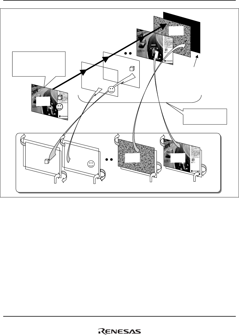
19. Display Unit (DU)
Rev.1.00 Jan. 10, 2008 Page 932 of 1658
REJ09B0261-0100
Frame
buffer 2
A double-buffer function is used to switch the frame buffer between drawing side and display side
The superpositioning
order can be specified
arbitrarily.
Background color can be specified.
Frame
buffer 1 Frame
buffer 2
Frame
buffer 1
Output planes are combined
and displayed according to
the superpositioning order
and blending mode for
each plane.
Frame
buffer 4
Frame
buffer 3
Display
side
Frame
buffer 4
Figure 19.2 Block Diagram of Plane Configuration and Superpositioning

19. Display Unit (DU)
Rev.1.00 Jan. 10, 2008 Page 933 of 1658
REJ09B0261-0100
19.4.2 Display On/Off
All plane display can be turned on and off using the DEN bit in DSYSR. When the DEN bit is 0,
the display data set in DOOR is displayed.
Display is turned on and off for planes 1 to 6 using DPPR. Under the following display conditions,
display data set in BPOR is displayed.
1. When display of all planes 1 to 6 is turned off
2. In an area with no plane for display, due to the display size and display position
3. When the pixels in a plane for display are all a transparent color
Table 19.5 Display On/Off of Plane 1 to 6
Display Plane Display Plane Priority Register (DPPR)
Plane 1 Plane 1 is selected in one among priority positions 1 to 6, and the
corresponding enable bit is set to 1
Plane 2 Plane 2 is selected in one among priority positions 1 to 6, and the
corresponding enable bit is set to 1
Plane 3 Plane 3 is selected in one among priority positions 1 to 6, and the
corresponding enable bit is set to 1
Plane 4 Plane 4 is selected in one among priority positions 1 to 6, and the
corresponding enable bit is set to 1
Plane 5 Plane 5 is selected in one among priority positions 1 to 6, and the
corresponding enable bit is set to 1
Plane 6 Plane 6 is selected in one among priority positions 1 to 6, and the
corresponding enable bit is set to 1
Note: Even if display on is set using DPPR, under the following conditions, the setting is handled
as display off, and the corresponding plane is not displayed.
• Planes for which the value set in PnDPXR is greater than the screen size (horizontal
display ending position register (HDE) - horizontal display start position register (HDS))
• Planes for which the value set in PnDPYR is greater than the screen size (vertical
display ending position register (VDE) - vertical display start position register (VDS))
• Planes for which the value set in PnDSXR is 0
• Planes for which the value set in PnDSYR is 0
• Planes for which the value set in PnMWR is 0
• Planes for which the value set in PnSPXR is equal to or greater than twice the value set
in PnMWR
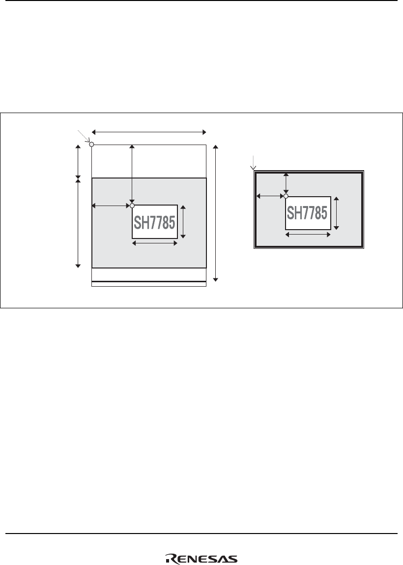
19. Display Unit (DU)
Rev.1.00 Jan. 10, 2008 Page 934 of 1658
REJ09B0261-0100
19.4.3 Plane Parameter
For each plane, a display area start position, memory width, display start position, and display size
are set using registers.
The followings are the schematic diagram of start positions and sizes related to planes and the
registers used for setting start positions and sizes.
1. MWX
2. DSA
5. SPX
6. SPY
7. DSX
8. DSY
3. WASPY
4. WAMWY
7. DSX
8. DSY
9. DPX
10. DPY
Monitor origin (upper left)
Memory parameters
Monitor parameters
11. MLY
Figure 19.3 Parameters

19. Display Unit (DU)
Rev.1.00 Jan. 10, 2008 Page 935 of 1658
REJ09B0261-0100
Table 19.6 Memory Parameter/ Monitor Parameter Setting Registers
No.
Names Used in the
Figure
Setting
Registers Description
1 MWX
(Plane memory width)
PnMWR The plane X-direction memory width is set
between 16 and 4096 pixels, in 16 pixel units.
2 DSA
(Display area start
address)
PnDSA0R and
PnDSA1R
The start address in memory area is set for
plane n.
3 WASPY
(Plane n wrap-around start
position)
PnWASPR The Y direction start position of the plane n
wrap-around area is set in raster line units,
with the address set by DSA as reference.
4 WAMWY
(Wraparound memory
width)
PnWAMWR The wrap-around Y-direction memory width is
set arbitrarily in the range 240 to 4095 lines.
5 SPX
(Start position X)
PnSPXR The distance in the X direction to the display
start position is set in pixel units, taking the
address set by DSA as the origin.
6 SPY
(Start position Y)
PnSPYR The distance in the Y direction to the display
start position is set in raster line units, taking
the address set by DSA as the origin.
7 DSX
(Display size X)
PnDSXR The X-direction display size of plane n is set in
pixel units.
8 DSY
(Display size Y)
PnDSYR The Y-direction display size of plane n is set in
raster line units.
9 DPX
(Display position X)
PnDPXR The X-direction distance to the display position
is set in pixel units, taking the upper-left corner
of monitor as the origin.
10 DPY
(Display position Y)
PnDPYR The Y-direction distance to the display position
is set in raster line units, taking the upper-left
corner of monitor as the origin.
11 MLY
(Memory length Y)
PnMLR The Y-direction memory area of plane n is set
in raster line units.

19. Display Unit (DU)
Rev.1.00 Jan. 10, 2008 Page 936 of 1658
REJ09B0261-0100
19.4.4 Memory Allocation
A display start address for the display screen can be set individually for each plane. Leading
addresses for the memory areas used are set in each of the display area start address registers.
In the display unit (DU), the display area start addresses 0 and 1 are used for each plane to
perform double-buffer control and display each plane.
Below is a list of display area start address registers used for each of the planes.
Table 19.7 Memory Allocation Registers
Display Plane Setting Register Name
Plane 1 display area start address register 0 P1DSA0 Plane 1
Plane 1 display area start address register 1 P1DSA1
Plane 2 display area start address register 0 P2DSA0 Plane 2
Plane 2 display area start address register 1 P2DSA1
Plane 3 display area start address register 0 P3DSA0 Plane 3
Plane 3 display area start address register 1 P3DSA1
Plane 4 display area start address register 0 P4DSA0 Plane 4
Plane 4 display area start address register 1 P4DSA1
Plane 5 display area start address register 0 P5DSA0 Plane 5
Plane 5 display area start address register 1 P5DSA1
Plane 6 display area start address register 0 P6DSA0 Plane 6
Plane 6 display area start address register 1 P6DSA1
19. Display Unit (DU)
Rev.1.00 Jan. 10, 2008 Page 937 of 1658
REJ09B0261-0100
19.4.5 Input Display Data Format
The following format is used for input color data used in display.
• 8 bit/pixel
A color palette index is used. The color palette is used to convert and display image data into
RGB data with 6 bits for each RGB color (RGB666).
The arrangement of data in memory is as follows.
A+3 A+2 A+1 A A A+1 A+2 A+3
31 23 15 7 0 31 23 15 7 0
Address A Index 3 Index 2 Index 1 Index 0 Address A Index 0 Index 1 Index 2 Index 3
Address A+4 Index 7 Index 6 Index 5 Index 4 Address A+4 Index 4 Index 5 Index 6 Index 7
Address A+8 Index 11 Index 10 Index 9 Index 8 Address A+8 Index 8 Index 9 Index 10 Index 11
Little endian Big endian
• 16 bit/pixel: RGB
The RGB levels are represented using 5 bits for R, 6 bits for G, and 5 bits for B (RGB565).
D15-D0 15 11 10 5 4 0
R G B
The arrangement of data in memory is as follows.
A+2 A A A+2
31 15 0 31 15 0
Address A RGB565 - 1 RGB565 - 0 Address A RGB565 - 0 RGB565 - 1
Address A+4 RGB565 - 3 RGB565 - 2 Address A+4 RGB565 - 2 RGB565 - 3
Address A+8 RGB565 - 5 RGB565 - 4 Address A+8 RGB565 - 4 RGB565 - 5
Little endian Big endian
19. Display Unit (DU)
Rev.1.00 Jan. 10, 2008 Page 938 of 1658
REJ09B0261-0100
• 16 bit/pixel: ARGB
The ARGB levels are represented using A:1, R:5, G:5, B:5 bits (ARGB555). In addition to the
RGB values, an alpha value is set. Blending control using the A value is valid when the
PnSPIM bit in PnMR is set to perform blending; when A = 1, blending is performed. When the
PnSPIM bit is not set to perform blending, blending is not performed even when A = 1.
D15-D0 15 14 10 9 5 4 0
A R G B
A+2 A A A+2
31 15 0 31 15 0
Address A ARGB555 - 1 ARGB555- 0 Address A ARGB555- 0 ARGB555- 1
Address A+4 ARGB555- 3 ARGB555- 2 Address A+4 ARGB555- 2 ARGB555- 3
Address A+8 ARGB555- 5 ARGB555- 4 Address A+8 ARGB555- 4 ARGB555- 5
Little endian Big endian
• YC
Image data has the format YC (YCbCr) = 4:2:2. A calculation circuit is used to convert each of
the 8 bits of the RGB colors of image data.
The YC data order corresponds to the UYVY format and YUYV format. The UYVY format
and YUYV format can be selected using the PnYCDF bits in PnMR.
The conversion formulae for each of the 8 bits of the RGB colors are as follows:
R = Y + 1.37 × (Cr - 128)
G = Y - 0.698 × (Cr - 128) - 0.336 x (Cb - 128)
B = Y + 1.73 × (Cb - 128)
16 ≤ Y ≤ 235
16 ≤ Cr ≤ 240
16 ≤ Cb ≤ 240
The following coefficients are used for the above formulae.
(1) 1.37 = 1.0101111
(2) 1.73 = 1.1011110
(3) 0.698 = 0.10110010
(4) 0.336 = 0.01010110
The internal processing is performed in 16-bit units.
Calculation is performed with fixed-point arithmetic and values are rounded down.

19. Display Unit (DU)
Rev.1.00 Jan. 10, 2008 Page 939 of 1658
REJ09B0261-0100
• UYVY format
A+3 A+2 A+1 A A A+1 A+2 A+3
31 23 15 7 0 31 23 15 7 0
Address A Y1 V0 Y0 U0 Address A U0 Y0 V0 Y1
Address A+4 Y3 V2 Y2 U2 Address A+4 U2 Y2 V2 Y3
Address A+8 Y5 V4 Y4 U4 Address A+8 U4 Y4 V4 Y5
Little endian Big endian
• YUYV format
A+3 A+2 A+1 A A A+1 A+2 A+3
31 23 15 7 0 31 23 15 7 0
Address A V0 Y1 U0 Y0 Address A Y0 U0 Y1 V0
Address A+4 V2 Y3 U2 Y2 Address A+4 Y2 U2 Y3 V2
Address A+8 V4 Y5 U4 Y4 Address A+8 Y4 U4 Y5 V4
Little endian Big endian

19. Display Unit (DU)
Rev.1.00 Jan. 10, 2008 Page 940 of 1658
REJ09B0261-0100
19.4.6 Output Data Format
When outputting digital RGB data from the display unit (DU), the display data format is expanded
into the RGB666 format before output. The format at the time of output is as indicated in the
following table.
Table 19.8 Output Data Format
Pin
Output
Data DR5 DR4 DR3 DR2 DR1 DR0 DG5 DG4 DG3 DG2 DG1 DG0 DG5 DG4 DG3 DG2 DG1 DG0
8 bits/
pixel
R (6 bits) G (6 bits) B (6 bits)
16 bits/
pixel
R (5 bits) 0 G (6 bits) B (5 bits) 0
ARGB R (5 bits) 0 G (5 bits) 0 B (5 bits) 0
YC→
RGB
R (upper 6 bits of the 8 bits) G (upper 6 bits of the 8 bits) B (upper 6 bits of the 8 bits)
19.4.7 Endian Conversion
The display unit (DU) can perform big-endian/little-endian conversion according to the setting of
the DSEC bit in DSYSR.
The internal data format in the display unit (DU) is fixed at little-endian; by setting the DSEC bit
in DSYSR to 1, display data arranged in big-endian format in memory is converted into little-
endian format and read.
The units for endian conversion (byte/word) is determined by the setting of the PnDDF bit in
PnMR.
Table 19.9 Endian Conversion
PnMR/PnDDF Data Format Units for Endian Conversion
00 8 bits/pixel Byte
01 16 bits/pixel Word
10 ARGB Word
11 YC Byte
19. Display Unit (DU)
Rev.1.00 Jan. 10, 2008 Page 941 of 1658
REJ09B0261-0100
Endian conversion in each of the units indicated below is shown in figure 19.4.
B0 B1 B2 B3 B4 B5 B6 B7
A
63 0
B8 B9 B10 B11 B12 B13 B14 B15
A + 8
Data
B7 B6 B5 B4 B3 B2 B1 B0
63 0
B15 B14 B12 B11 B10 B9 B8
127 64
W0 W1 W2 W3
63 0
W4 W5 W6 W7
63 0
127
W3 W2 W1 W0
W7 W6 W5 W4
B13
Address
SHwy bus (big endian)
Display data in the display unit (DU)
A
A + 8
Data
Address
SHwy bus (big endian)
Display data in the display unit (DU)
Endian Conversion in Byte Units:
PnDDF = 0 0: 8 bits/pixel
PnDDF = 1 1: YC
Endian Conversion in Word Units:
PnDDF = 0 1: 16 bits/pixel
PnDDF = 1 0: ARGB
Figure 19.4 Endian Conversion

19. Display Unit (DU)
Rev.1.00 Jan. 10, 2008 Page 942 of 1658
REJ09B0261-0100
19.4.8 Color Palettes
8 bits/pixel data employs color palettes. Four color palettes can be used; these are called color
palette 1, color palette 2, color palette 3, and color palette 4.
The color palette used in each plane can be set to any among color palette 1, color palette 2, color
palette 3, and color palette 4 using the PnCPSL bits in PnMR. Each of the color palettes consists
of two alternate buffers; one serves as a display buffer, and the other is for CPU access. After
setting each color palette, by setting the color palette switching enable bits (CP4CE, CP3CE,
CP2CE, CP1CE) in CPCR to 1, the color palette thus set becomes valid at the next VSYNC falling
edge (internal update timing), or upon display reset (when the DRES bit in DSYSR is changed
from 1 to 0).
Notes on Use of Color Palettes:
1. Because palettes consist of alternate buffers, complete overwriting is necessary upon a color
palette update. However, when the details of color palette updates are being managed, there is
no problem with overwriting only the relevant part.
2. Upon completion of color palette settings, the switching enable bit must always be set to 1.
3. When reading a color palette which has been written from the CPU, reading should be
performed before setting the switching enabled bit to 1. If read after setting the bit to 1, there is
the possibility that different palette contents may be read after palette switching occurs.
Procedure For Setting A Color Palette:
• Procedure for switching from the initial state
The initial state (after power-on reset) is the display reset state.
A. Set the registers of the display unit (DU).
B. Set either color palette 1, color palette 2, color palette 3, or color palette 4.
C. After setting the color palette, set the color palette switching enable bit to 1.
D. Cancel the display reset.
• Procedure for switching from display state
In the display state, the DRES bit and DEN bit in the DSYSR are 0 and 1 respectively.
A. Confirm that the color palette switching enable bit is 0.
B. Set either color palette 1, color palette 2, color palette 3, or color palette 4.
C. After setting the color palette, set the color palette switching enable bit to 1.

19. Display Unit (DU)
Rev.1.00 Jan. 10, 2008 Page 943 of 1658
REJ09B0261-0100
19.4.9 Superpositioning of Planes
For each plane, three types of combined superpositioning are possible: α blending, transparent
colors, and EOR operations. By setting the PnSPIM bits in PnMR, the superpositioned display
type can be selected.
However, α blending and EOR operation cannot be performed simultaneously on the same plane.
α blending and EOR operations are performed after expanding the display data format into
RGB888 format.
Complementary formats for the different input display data formats are indicated in table 19.11.
α blending and EOR operations are performed in order from lower planes to higher planes. Figure
19.5 is a block diagram illustrating this procedure.
Table 19.10 Superpositioning
PnSPIM Superpositioning
000 Transparency processing is performed for the specified plane.
When the specified plane is a transparent color, the lower plane is displayed.
(Initial value)
001 Blending of the specified plane with the lower plane is performed.
When the specified plane is a transparent color, blending is not performed and the
lower plane is displayed.
010 EOR operation of the specified plane and the lower plane is performed.
When the specified plane is a transparent color, EOR operation is not performed
and the lower plane is displayed.
011 Setting prohibited
100 Transparency processing is not performed for the specified plane.
The specified plane is displayed.
101 Blending of the specified plane with the lower plane is performed.
Transparent color specification for the specified plane is ignored, and blending of
all the pixels in the specified plane with the lower plane is performed.
110 EOR operation of the specified plane and the lower plane is performed.
Transparent color specification for the specified plane is ignored, and EOR
operation of all the pixels in the specified plane and the lower plane is performed.
111 Setting prohibited
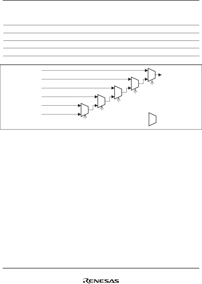
19. Display Unit (DU)
Rev.1.00 Jan. 10, 2008 Page 944 of 1658
REJ09B0261-0100
Table 19.11 RGB888 Bit Configuration in Each Display Data Format
Data Format R (8 bits) G (8 bits) B (8 bits)
8 bits/pixel R (6 bits) 0 0 G (6 bits) 0 0 B (6 bits) 0 0
16 bits/pixel R (5 bits) 0 0 0 G (6 bits) 0 0 B (5 bits) 0 0 0
ARGB R (5 bits) 0 0 0 G (5 bits) 0 0 0 B (5 bits) 0 0 0
YC→RGB R (8 bits) G (8 bits) B (8 bits)
Plane PnSPIM with priority 4
Plane with priority 1
Plane with priority 2
Plane with priority 3
Plane with priority 4
Plane with priority 5
Plane with priority 6
Output display data
Plane PnSPIM with priority 3
Plane PnSPIM with priority 2
Plane PnSPIM with priority 1
Superposition
processing circuit
The priority is set in DPPR. Plane PnSPIM with priority 5
Figure 19.5 Plane Processing Sequence in α Blending and EOR Operation
When the format of display data for α blending or EOR operation is 8 bits/pixel, after selection in
advance of the color palette to be used, the α blending or EOR operation on/off should be
specified. At this time, when both planes for α blending or for EOR operation have the same color
palette selected (color palette contention), only the specified plane is displayed, with no α
blending or EOR operation performed. When display of all lower planes is turned off, the
specified plane is displayed. That is, blending or EOR operation of the specified plane with the
display data specified in BPOR is not performed.
α Blending: In α blending, blending processing is performed according to the alpha (α) value set
by the PnALPHA bits in PnALPHAR, the alpha (α) value set by the blend ratio bits in the color
palette, or the alpha (α) value of the input display data.
Blending result = (α × specified plane + (H'100-α) × lower plane)/H'100
Notes: 1. In the above formula, the blending result, α, the specified plane, and the lower plane
are all given as 8-bit data.
2. When 0 is set as the alpha value, only the lower plane is displayed.
3. Approximation compensation is not performed. Alpha value is equal to H'FF, specified
plane is equal to H'FF and lower plane equal to H’00, and then the result is H'FE.

19. Display Unit (DU)
Rev.1.00 Jan. 10, 2008 Page 945 of 1658
REJ09B0261-0100
When the PnDDF bit in PnMR is set to ARGB, and moreover the PnSPIM bit in PnMR is set to
perform blending, α blending is performed according to the A value of the input ARGB data
format.
Transparent Colors: For each plane, transparent color processing can be performed between the
specified plane and the lower plane by setting PnSPIM bit in PnMR to 0. However, in YC format
transparent color processing cannot be performed.
When the input display data and register value match, a color is judged to be a transparent color.
• In 8 bits/pixel mode
When the PnTC bit in PnMR is 0 (initial value), transparent color processing is performed
according to the setting in the plane n transparent color 1 register (PnTC1R). When the PnTC
bit PnMR is 1, up to a maximum 16 colors can be simultaneously specified for each of color
palette 1, color palette 2, color palette 3, color palette 4 according to the settings in CP1TR to
CP4TR. Only the indexes H'00 to H'0F can be specified as transparent colors; H'10 to H'FF
cannot be specified as transparent colors.
The color palette 1 to 4 transparent color registers can be selected using the PnCPSL bits in
PnMR.
• In 16 bits/pixel mode and ARGB mode
Transparent color processing is performed according to PnTC2R, regardless of the setting of
the PnTC bit in PnMR.
In the case of ARGB, bits 14 to 0 of PnTC2R are compared, and bit 15 is ignored.
The above is summarized in table 19.12, which indicates the transparent color specification
registers which are valid when the PnTC bit in PnMR is 0 and 1.

19. Display Unit (DU)
Rev.1.00 Jan. 10, 2008 Page 946 of 1658
REJ09B0261-0100
Table 19.12 Transparent Color Specification Registers
Data Format
Transparent Color
Specification Bit
Color Palette Select
Bit
Transparent Color
Specification Register
⎯ (PnMR) /PnTC (PnMR) /PnCPSL ⎯
0 ⎯ PnTC1R
1 00 CP1TR
1 01 CP2TR
1 10 CP3TR
8 bits/pixel
1 11 CP4TR
16 bits/pixel ⎯ ⎯ PnTC2R
ARGB ⎯ ⎯ PnTC2R
EOR Operation: EOR operation of the specified plane with the lower plane is performed.
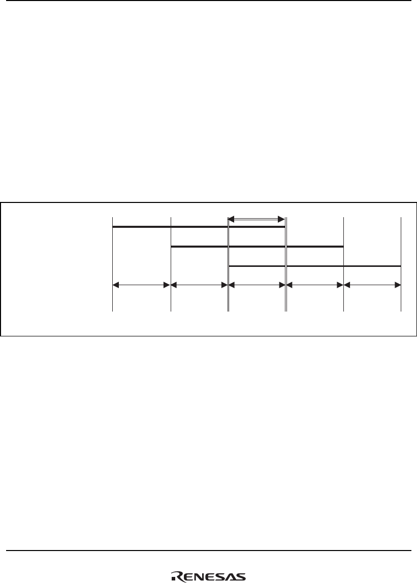
19. Display Unit (DU)
Rev.1.00 Jan. 10, 2008 Page 947 of 1658
REJ09B0261-0100
19.4.10 Display Contention
Color Palette Contention: When performing α blending and EOR operations, if the same color
palette is selected for both planes with the input display data format at 8 bits/pixel, color palette
contention may occur. This is because contention decisions occur not in plane units, but in pixel
units.
Figure 19.6 shows contention for a case in which data for plane 1, plane 2, and plane 3 is 8
bits/pixel, α blending is specified for plane 1 and EOR operation is specified for plane 2, and the
same color palette is selected for the three planes. (It is assumed that there are no transparent-color
pixels in plane 1, plane 2, or plane 3.)
When contention occurs, α blending and EOR operations become invalid, and the plane with the
highest priority is displayed.
A
Plane 1 (α blending)
Plane 2 (EOR operation)
Plane 3
Legend:
P1: Plane 1
P2: Plane 2
P3: Plane 3
No contention
P1 is displayed
P1 and P2
contention
P1 is displayed
P1, P2, and P3
contention
P1 is displayed
P2 and P3
contention
P2 is displayed
No contention
P3 is displayed
Note: Bold black lines indicate the display area.
Figure 19.6 Color Palette Contention
(When Same Color Palette Is Selected for Multiple Planes)
Figure 19.7 summarizes the display results when combining color palette selection and transparent
colors in the display section A in Figure 19.6.
• P1αP2 shows the result of α blending of plane 1 and plane 2.
• P2⊕P3 shows the result of an EOR operation on plane 2 and plane 3.
• P1α (P2⊕P3) shows the result of α blending of plane 1 with the result of an EOR operation on
plane 2 and Plane 3.
• BPOR shows display data in the background color register.
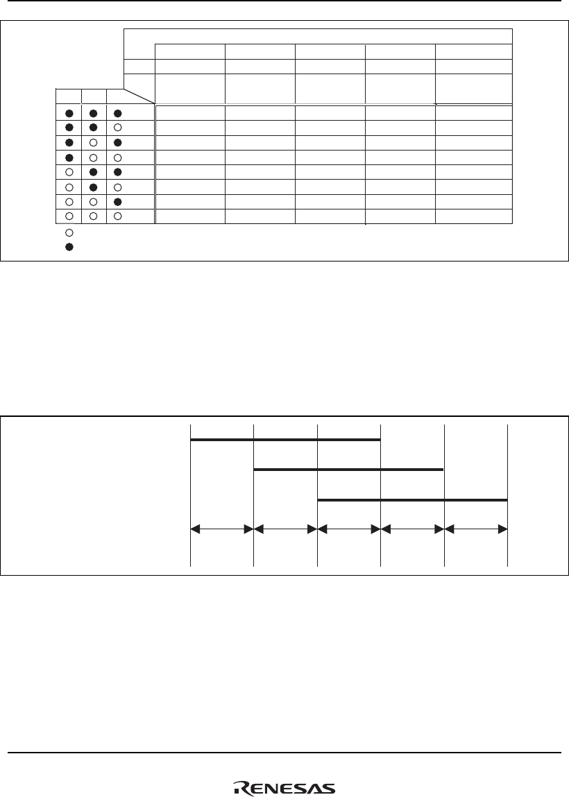
19. Display Unit (DU)
Rev.1.00 Jan. 10, 2008 Page 948 of 1658
REJ09B0261-0100
P1
P1 P2 P3
ΔΔΔX X
P2 ΔΔXΔX
P3 ΔXΔΔX
P1
P1
P1
P1
P2
P2
P3
BPOR
P1
P1
P1αP3
P1
P2⊕P3 P2⊕P3
P2
P3
BPOR
P1αP2
P1αP2
P1
P1
P2
P3
BPOR
P1αP2
P1αP2
P1αP3
P1
P2
P2
P3
BPOR
P1(P2⊕P3)
P1αP2
P1αP3
P1
P2⊕P3
P2
P3
BPOR
Color palette selection Δ: Same color palette selected; X: Different color palette selected
Transparent color
Non-transparent color
Figure 19.7 Results of Display Combining Color Palette Selection and Transparent Colors
YC Data Contention: The display unit (DU) has only one YC-RGB conversion circuit internally,
and so YC-RGB conversion cannot be performed simultaneously for two or more planes. When
there are pixels requiring YC-RGB conversion on two or more planes simultaneously, the pixels
on the uppermost plane are YC-RGB converted, and the lower plane is not displayed.
Figure 19.8 describes YC-RGB conversion when the data for three planes is in YC format.
Plane 1 (YC data)
Plane 2 (YC data)
Plane 3 (YC data)
YC-RGB conversion plane Plane 1 Plane 1 Plane 1 Plane 2 Plane 3
Figure 19.8 YC Data Contention
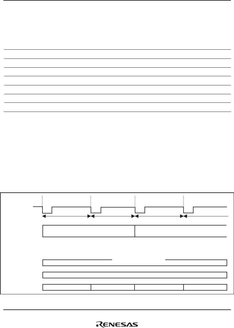
19. Display Unit (DU)
Rev.1.00 Jan. 10, 2008 Page 949 of 1658
REJ09B0261-0100
Plane Priority Order: The display priority order for planes is set using DPPR; if one plane is set
in two or more places in the priority order, the place with highest priority is selected.
For example, if the setting in DPPR is H'00CBD888, then the results of the priority order and
display on/off settings are as follows.
Plane with priority 1 Plane 1
Plane with priority 2 No corresponding plane
Plane with priority 3 No corresponding plane
Plane with priority 4 Plane 6
Plane with priority 5 Plane 4
Plane with priority 6 Plane 5
Display off planes Plane 2 and plane 3
19.4.11 Blinking
For each plane, blinking operation can be performed by using the display area start address 0 and
1 registers.
Usually, double buffer control is performed for each plane according to the setting of the PnBM
bit in PnMR. However, blinking is performed with the period specified by the PnBTA and PnBTB
bits in PnBTR by setting the PnBM bits in PnMR to 10 (Auto display change mode (blinking
mode)). If the PnBTA and PnBTB bits are set to 0, operation is the same as when set to 1.
(m-1)th frame m-th frame First frame Second frame
VSYNC
Operation of
the display unit (DU) A0 is displayed on screen A1 is displayed on screen
A0: Display area start address 0
A1: Display area start address 1
PnBTA (A0 display period is set)
PnBTB (A1 display period is set)
(Internal counter)
Blinking period
setting
BTA-1 BTA 0 1
Buffer switching performed
according to blinking period
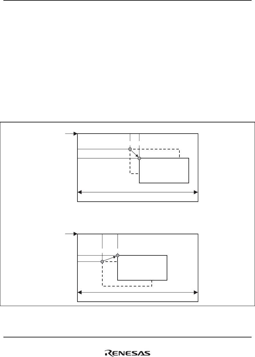
19. Display Unit (DU)
Rev.1.00 Jan. 10, 2008 Page 950 of 1658
REJ09B0261-0100
19.4.12 Scroll Display
By setting display area and display screen sizes and start positions independently for each plane,
smooth scroll processing can be performed independently for each plane.
The display can be scrolled by cyclically setting the plane n display start position X, Y values
(coordinates specified by PnSPXR and PnSPYR), taking as the origin the leading address in
memory specified by PnDSA0R and PnDSA1R for each plane.
Figure 19.9 summarizes display scrolling. The display is scrolled by setting the display start
position from A to B.
Note: Display sizes and other area settings for each plane should be set such that there is no data
display outside the memory configuration area.
Plane 1 display area start address
A
B
Memory width
Plane 6 display area start address
A
B
Memory width
.
.
.
Display start position
Display start position
Figure 19.9 Schematic Diagram of Scroll Display
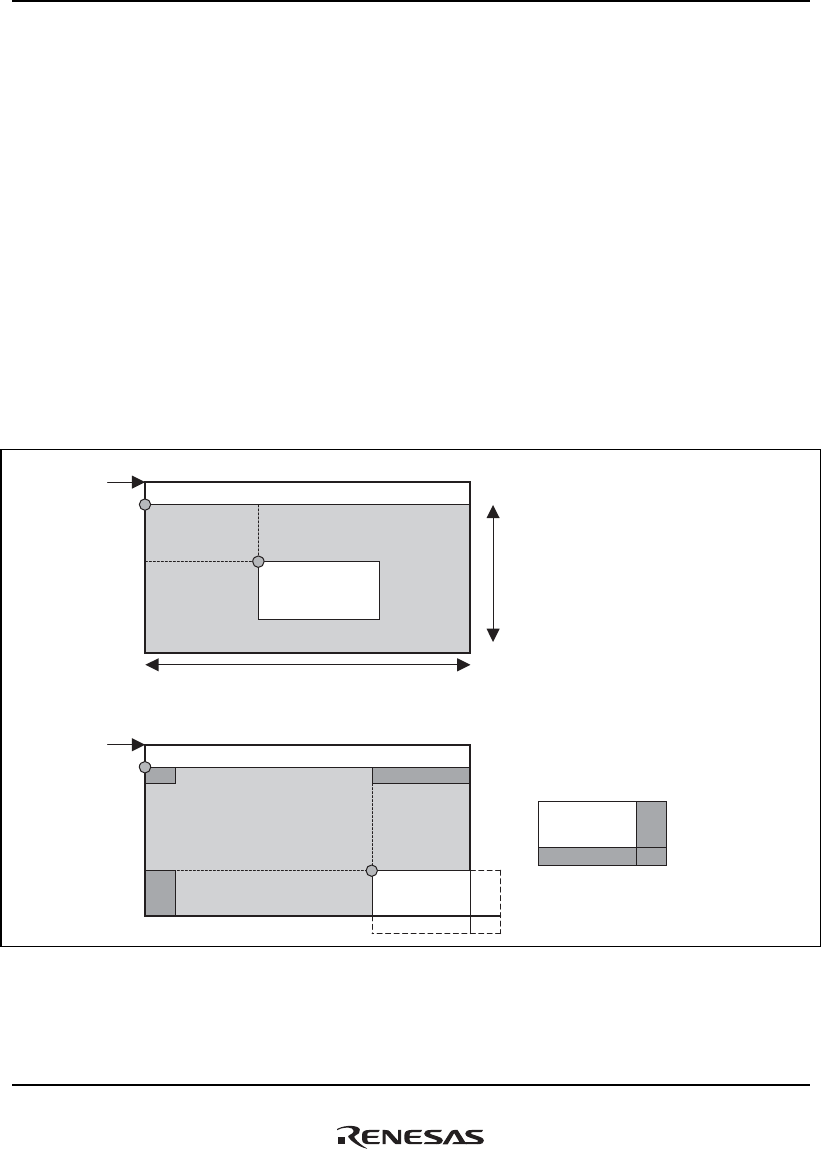
19. Display Unit (DU)
Rev.1.00 Jan. 10, 2008 Page 951 of 1658
REJ09B0261-0100
19.4.13 Wraparound Display
In addition to display scrolling, wrap-around display, which can be used in spherical scrolling, is
possible for each plane. When enabling wrap-around display, the PnWAE bit in PnMR is set. As a
result of changing the plane n display start position X, Y (the plane n start position X set in
PnSPXR and the plane n start position Y set in PnSPYR) in order to scroll the display, even when
plane n overflows the wrap-around area, the wrap-around area is seen as a spherical surface in
wrap-around display, as in figure 19.10, and the part overflowing is complemented and displayed.
The method used to specify the wrap-around area is described below.
1. The leading address of the memory used for plane n is specified in PnDSA0R and PnDSA1R.
2. With the beginning of the specified memory as origin, the upper-left coordinates of the wrap-
around area are specified in PnWASPR. The X-direction width of the wrap-around area is the
memory width set in PnMWR.
3. The Y-direction width of the wrap-around area is set in PnWAMWR.
Plane n display area start address
Plane n wrap-around start position
Wrap-around
memory width Y
Plane n display start position
Wrap-around display
Memory width
Plane n display start position
1
2
43
1
34
2
Figure 19.10 Schematic Diagram of Wraparound Display
Note: When wrap-around display is disabled (when the PnWAE bit in PnMR is 0), the part
overflowing the wrap-around area becomes the color specified by BPOR, and
superposition processing using this color is performed.
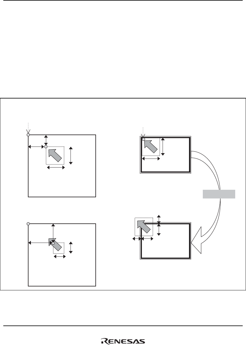
19. Display Unit (DU)
Rev.1.00 Jan. 10, 2008 Page 952 of 1658
REJ09B0261-0100
19.4.14 Upper-Left Overflow Display
For each plane, a display start position in memory (PnSPXR, PnSPYR) and display size
(PnDSXR, PnDSYR) can be set arbitrarily, so that by combining and using these registers, areas
overflowing the upper-left relative to the monitor origin (upper-left corner) can be displayed
without overwriting display data in memory.
For a picture of size (DSX, DSY) and with start position (SPX, SPY), by setting the size to (DSX-
ΔX, DSY-ΔY) and the start position to (SPX+ΔX, SPY+ΔY), the ΔX part overflowing on the left
side and the ΔY part overflowing on top can be displayed. At this time, the display position
(PnDPXR, PnDPYR) is fixed at 0.
SPY
SPX DSY
DSX
Monitor
SPY + ΔY
SPX + ΔX DSY - ΔY
DSX - ΔX
Monitor
DSX
DSY
DSY - ΔY
DSX - ΔX
ΔY
ΔX
Display data in memory Monitor screen
(DPX,DPY)=(0,0)
(DPX,DPY)=(0,0)
Display area start address
Monitor origin
Overflow display
Figure 19.11 Schematic Diagram of Upper-Left Overflow Display
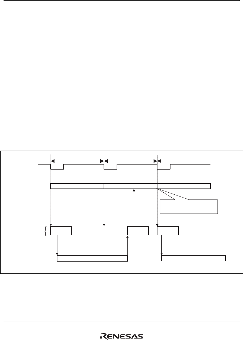
19. Display Unit (DU)
Rev.1.00 Jan. 10, 2008 Page 953 of 1658
REJ09B0261-0100
19.4.15 Double Buffer Control
The double buffer control of the display unit (DU) includes two types of functions, which are a
manual display change mode in which display switching is all controlled by software, and an auto
display change mode to realize blinking.
In the case of manual display change mode, the display change is performed in frame units for
non-interlaced and interlaced sync display, and in field units for interlaced sync & video display.
In the case of auto display change mode, all switching is performed in field units.
Manual Display Change Mode: In manual display change mode, display frame switching is
controlled by software. Display switching can either be performed by software using the PnDC bit
in PnMR, or by setting the buffer 0 or buffer 1 start address in PnDSA0R and PnDSA1R indicated
by the DFBn bit in DSSR.
When making a transition from this mode to another mode, the PnDC bit should always be set to 1
first.
The following shows a control example for the manual display mode.
VSYNC
(Non-interlaced)
Display screen
operation
A0 display A0 display A1 display
First frame Second frame Third frame
Interrupt
processing
Interrupt
processing
Interrupt
processing
Start of
transfer
Start of
transfer
CPU operation
A0: Display area start address 0
A1: Display area start address 1
VBK: VBK bit in DSSR
Transfer of display data for A1 Transfer of display data for A0
Display is switched by
the PnDC bit or DSAR
at the falling edge of VSYNC.
Display data
transfer by a
VBK interrupt
If display data
transfer for B1 has
not been completed,
a VBK interrupt is
ignored.
PnDC bit is set to 1,
or
DSAR address is
set.
The PnDC bit is
set by a transfer
end interrupt.
Auto Display Change Mode: For information on the auto display change mode, refer to section
19.4.11, Blinking.

19. Display Unit (DU)
Rev.1.00 Jan. 10, 2008 Page 954 of 1658
REJ09B0261-0100
19.4.16 Sync Mode
In order to facilitate synchronization with external equipment, in addition to master mode, a TV
synchronization function is provided. Selection of master mode and TV sync mode is performed
using the TVM bit in DSYSR. Regardless of the synchronization method, the position of the
falling edge of the vertical sync signal (VSYNC) set by VSPR is detected and is reflected in the
FRM bit and VBK bit in DSSR.
Master Mode (Internal Sync Mode): By setting the period and pulse width of the horizontal and
vertical sync signals (HSYNC, VSYNC) in the display timing generation register, the
corresponding waveforms are output. Also, display data is output in sync with these signals.
When in interlaced sync mode and interlaced sync & video mode, a signal is output to the ODDF
pin indicating odd/even fields.
TV Sync Mode (External Sync Mode): In TV sync mode, display data is output in sync with a
horizontal sync signal and vertical sync signal (EXHSYNC, EXVSYNC) input from a TV, video,
or other external sync signal generation circuit. Display data is output with reference to the falling
edge of the EXHSYNC signal and the rising edge of the EXVSYNC signal.
The horizontal sync signal, vertical sync signal, and clock signal from the external sync signal
generation circuit are input to the HSYNC, VSYNC, and DCLKIN pin, respectively. CSYNC is at
high level. When in interlaced sync mode and interlaced sync & video mode, a signal should be
input to the ODDF pin indicating odd/even fields. When in non-interlaced mode, the input to the
ODDF pin should be fixed at low level or at high level.
When operating the unit in TV sync mode also, values must be set in HCR, HSWR, VCR, and
VSPR (display timing generation registers).
When the EXVSYNC signal is input, either before or after completion of display of the display
size portion set in the display unit (DU), the display unit (DU) performs vertical display
completion operation and transitions to control for the next screen. When the EXVSYNC signal is
not input, the unit continues to wait for the EXVSYNC signal while remaining in the vertical
blanking interval (auto-control is not performed). Similarly, when the EXHSYNC signal is input
the display unit (DU) performs horizontal display completion operation and transitions to control
for the next raster line; but if the EXHSYNC signal is not input, the unit continues to wait for the
EXHSYNC signal while remaining in the horizontal blanking interval (auto-control is not
performed).
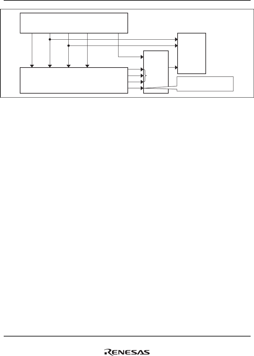
19. Display Unit (DU)
Rev.1.00 Jan. 10, 2008 Page 955 of 1658
REJ09B0261-0100
TV (sync signal generation circuit): Master
Clock HSYNC
VSYNC R,G,B
This LSI: Slave
DCLKIN DR5-DR0
DG5-DG0
DB5-DB0
Input 2
Input 1
Output
Display
Switching between master
(input 2) and slave (input 1)
by CDE.
VSYNCODDF
CDE
HSYNC
Field signal
Figure 19.12 Signal Flow in TV Sync Mode
Sync Method Switching Mode: When switching from master mode into TV sync mode, or from
TV sync mode into master mode, when necessary this mode should be switched into first. Even if
a transition to this mode is not made first, switching of the synchronization method is possible.
In this mode, input/output pins connected to the display unit (DU) are for input, and so pin
collision can be avoided. Also, in this mode no display operation is performed, and the internal dot
clock is stopped, so that disorder in the input dot clock has no effect on display operation.
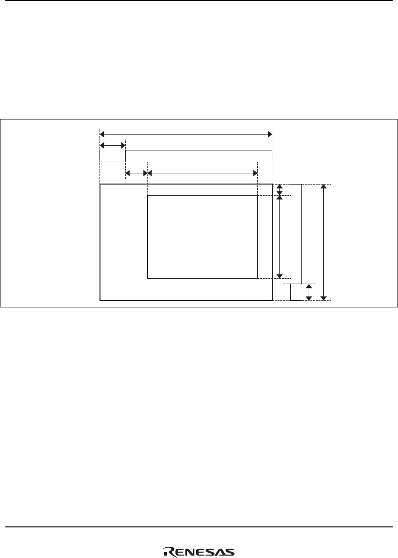
19. Display Unit (DU)
Rev.1.00 Jan. 10, 2008 Page 956 of 1658
REJ09B0261-0100
19.5 Display Control
19.5.1 Display Timing Generation
In the display unit (DU), display timing is generated for the horizontal direction and vertical
direction of the display screen. Display timing is set by using display timing generation registers.
Figure 19.13 shows the display timing in non-interlaced mode. Here, the display screen is defined
in terms of the variables of Table 19.13.
hc
hsw
xs xw
ys yw
vc
vsw
Display area
HSYNC
VSYNC
Figure 19.13 Display Timing Generation for Horizontal Direction and Vertical Direction of
Display Screen

19. Display Unit (DU)
Rev.1.00 Jan. 10, 2008 Page 957 of 1658
REJ09B0261-0100
Table 19.13 Variables Defined in Display Screen
Variables Contents Units
hc*1 Horizontal scan period Dot clock
hsw Horizontal sync pulse width Dot clock
xs From rise of HSYNC to display start position in the
horizontal direction of the display screen
Dot clock
xw Display width per 1 raster of display screen Dot clock
vc*2 Vertical scan period Raster line
vsw Vertical sync pulse width Raster line
ys From rise of VSYNC to display start position in the
vertical direction of the display screen
Raster line
yw Vertical display period of display screen Raster line
Notes: 1. Should be set such that hsw + xs + xw < hc + 18 (decimal)
2. Should be set such that vsw + ys + yw < vc
The display timing generation register settings are different depending on the scan method and
synchronization method. Hence the value of the display timing generation register should be set
after performing calculations like those indicated in Table 19.14.
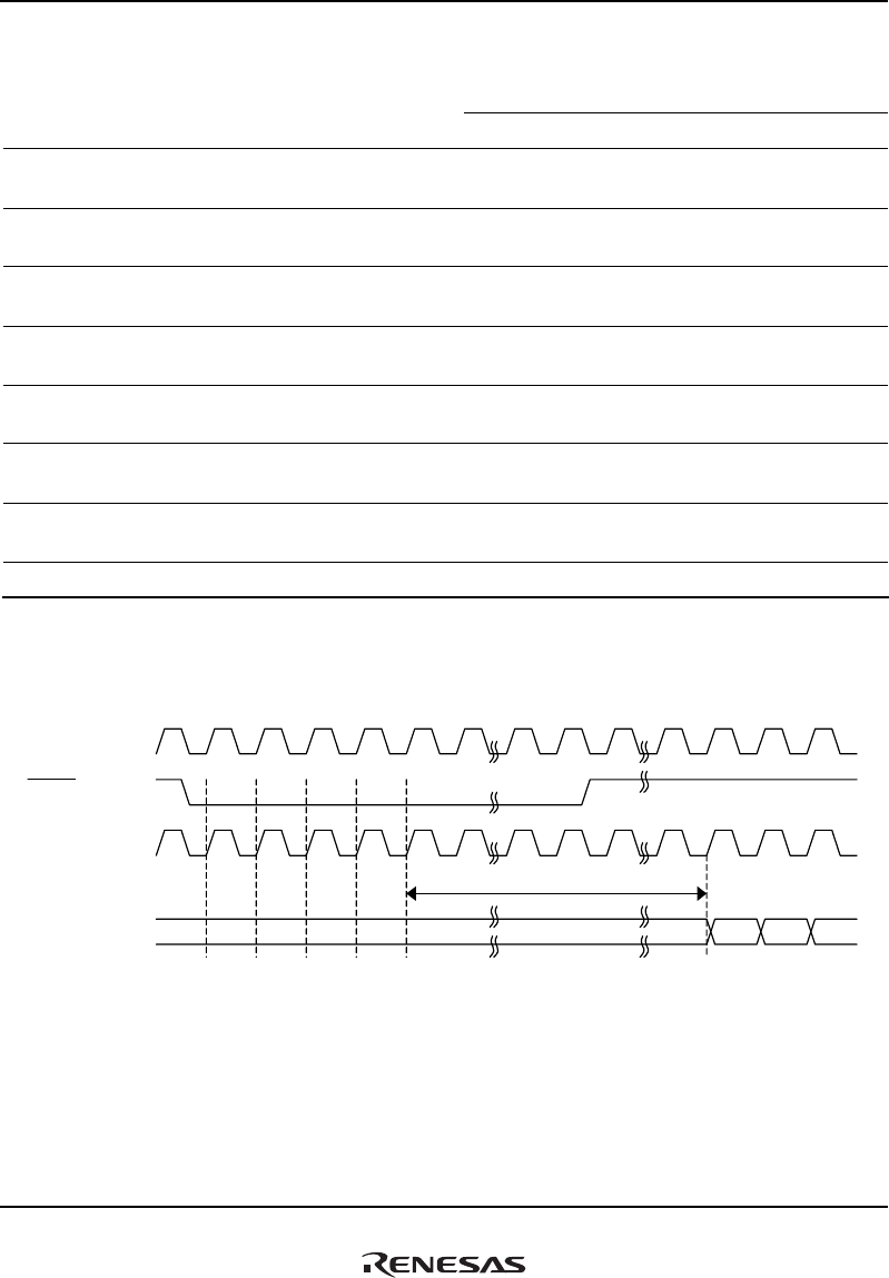
19. Display Unit (DU)
Rev.1.00 Jan. 10, 2008 Page 958 of 1658
REJ09B0261-0100
Table 19.14 Correspondence Table of Settings of Display Timing Generation Registers
Synchronization Method
Register Name Bit Name Master Mode TV Sync Mode
Horizontal display start position
register (HDSR)
HDS hsw + xs - 19 hsw + xs – 24 *2
Horizontal display end position
register (HDER)
HDE hsw + xs – 19 + xw hsw + xs – 24 + xw *2
Vertical display start position register
(VDSR)
VDS ys – 2 *3 ys – 2 *3
Vertical display end position register
(VDER)
VDE ys – 2 + yw ys – 2 + yw
Horizontal synchronous pulse width
register (HSWR)
HSW hsw - 1 hsw - 1
Horizontal scan period register
(HCR)
HC hc - 1 hc - 1
Vertical synchronous position
register (VSPR)
VSP vc – vsw - 1 vc – vsw - 1
Vertical scan period register (VCR) VC vc - 1 vc - 1
Notes: The numerical values in the above table are decimal numbers.
1. In all scan modes, VDS, VDE, VSP, VC settings are in single-field units.
2. The values of HDS and HDE are from the fourth rising edge of DCLKOUT after
detection of the falling edge of HSYNC through the rising edge of DCLKOUT.
DCLKIN(input)
DR5-DR0(output)
DG5-DG0(output)
DB5-DB0(output)
hsw + xs
D0 D1 D2
HSYNC( input)
DCLKOUT(output)
3. VDS should be set to 1 or greater.
4. HC should be set so as to satisfy HC > HDE.
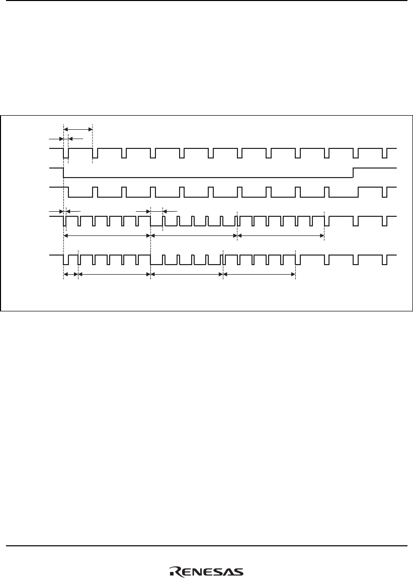
19. Display Unit (DU)
Rev.1.00 Jan. 10, 2008 Page 959 of 1658
REJ09B0261-0100
19.5.2 CSYNC
When in master mode, a CSYNC (composite sync) signal is output. EQWR is used to set the low-
level pulse width of the CSYNC equal pulse. SPWR is used to set the low-level pulse width of the
CSYNC separation pulse.
The CSYNC waveform is selected using the CSY bit in DSMR.
HSW
HSYNC
VSYNC
CSYNC
(CSY = 00)
EQW
(CSY = 10)
(CSY = 11)
HC
SPW
1/2HC
When HC is odd, it is rounded to an even value.
Equivalent pulse:
2.5 rasters
Separation pulse:
2.5 rasters
Equivalent pulse:
2.5 rasters
Equivalent pulse:
3 rasters
Separation pulse:
3 rasters
Equivalent pulse:
3 rasters
Figure 19.14 CSYNC Timing Chart (Non-Interlaced Mode, First Half of Interlace Frame)
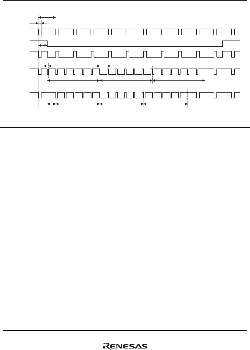
19. Display Unit (DU)
Rev.1.00 Jan. 10, 2008 Page 960 of 1658
REJ09B0261-0100
VSYNC
CSYNC
(CSY = 00)
EQW
(CSY = 10)
(CSY = 11)
1/2HC
1/2HC
SPW
HSW
HSYNC
HC
Equivalent pulse:
2.5 rasters
Separation pulse:
2.5 rasters
Equivalent pulse:
2.5 rasters
Equivalent pulse:
3 rasters
Separation pulse:
3 rasters
Equivalent pulse:
3 rasters
When HC is odd, it is rounded to an even value.
Figure 19.15 CSYNC Timing Chart (Last Half of Interlace Frame)

19. Display Unit (DU)
Rev.1.00 Jan. 10, 2008 Page 961 of 1658
REJ09B0261-0100
19.5.3 Scan Method
The scan method can be selected from among non-interlaced mode, interlaced sync mode, and
interlaced sync & video mode. The mode is selected using the SCM bit in DSYSR.
• Non-interlaced mode
In this scan method, one frame consists of a single field.
• Interlaced sync mode
In this scan method, one frame consists of two fields. The two fields are an even field and an
odd field, displaying the same data.
• Interlaced sync & video mode
In this scan method, one frame consists of two fields. The two fields are an even field and an
odd field, displaying different data.
The ODEV bit in DSMR is used to set the display order of fields in interlaced sync mode and in
interlaced sync & video mode. When the ODEV bit is 0, the display order for one frame is odd
field, then even field; when the ODEV bit is 1, the order for one frame is even field, then odd
field.
When in master mode, high level is output from the ODDF pin during even field display, and low
level is output during odd field display. When in TV sync mode, high level is input to the ODDF
pin to cause display of the even field, and low level is input to cause display of the odd field.
Note: When non-interlaced mode is selected in TV sync mode, the ODDF pin should be fixed at
low level or high level.
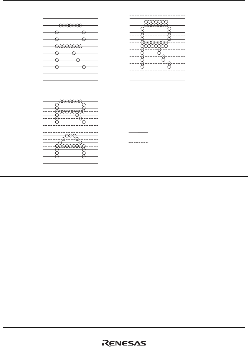
19. Display Unit (DU)
Rev.1.00 Jan. 10, 2008 Page 962 of 1658
REJ09B0261-0100
Raster scanned in an odd field
Raster scanned in an even field
00
01
02
03
04
05
06
07
08
09
00
01
02
03
04
05
06
07
08
09
00
01
02
03
04
05
06
07
08
09
00
02
04
06
08
0A
0C
0E
10
12
01
03
05
07
09
0B
0D
0F
11
13
Interlaced sync & video mode
Non-interlaced mode Interlaced sync mode
Figure 19.16 Example of Display in Each Scan Mode
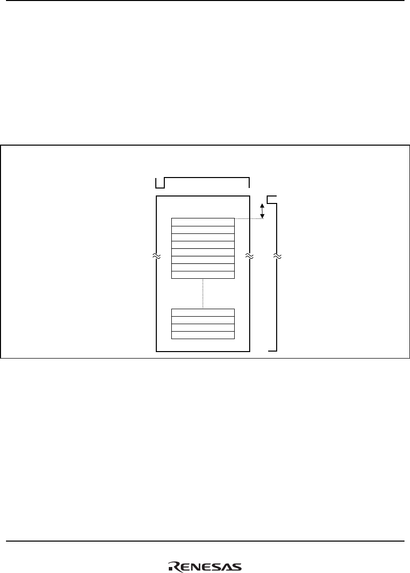
19. Display Unit (DU)
Rev.1.00 Jan. 10, 2008 Page 963 of 1658
REJ09B0261-0100
• Example of vertical scan period
Non-interlaced mode: 1/60 second/field, 1/30 second/field
Interlaced mode: 1/30 second/frame
Interlaced sync & video mode: 1/30 second/frame
• Display in non-interlaced method
In this method, all lines are displayed at once without providing intervals between input video
signals.
This input method is for monitors capable of high-resolution display.
0
1
2
3
476
477
HSYNC
VDS
VSYN
C
Display in non-interlaced mode
The ODEV and ODDF pins are not used.
4
5
6
7
478
479
Figure 19.17 Display in Non-Interlaced Method
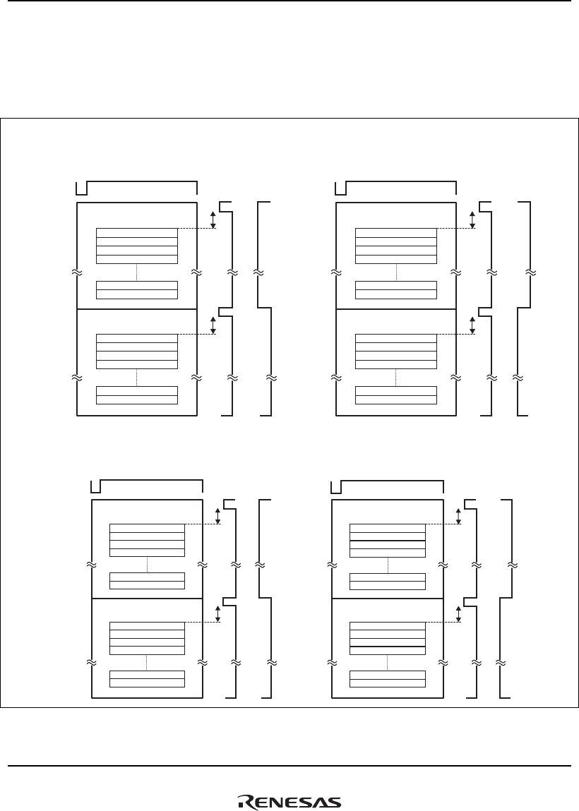
19. Display Unit (DU)
Rev.1.00 Jan. 10, 2008 Page 964 of 1658
REJ09B0261-0100
• Display in interlaced method
At every scan period VC of the input video signal, even lines and odd lines are switched and
displayed in alternation, and a single screen (one frame) is combined and displayed (with the
afterimage of the preceding VC) with a period of 2VC. This is the normal TV input method.
1. Display in interlaced sync mode
When one frame is configured as shown below,
clear the ODEV bit to 0.
· The first field is an odd field (the ODDF pin is low)
· The second field is an even field (the ODDF pin is high)
When one frame is configured as shown below,
set the ODEV bit to 1.
· The first field is an even field (the ODDF pin is high)
· The second field is an odd field (the ODDF pin is low)
2. Display in interlaced sync & video mode
When one frame is configured as shown below,
clear the ODEV bit to 0.
· The first field is an odd field (the ODDF pin is low)
· The second field is an even field (the ODDF pin is high)
When one frame is configured as shown below,
set the ODEV bit to 1.
· The first field is an even field (the ODDF pin is high)
· The second field is an odd field (the ODDF pin is low)
0
1
2
3
238
239
HSYNC
VDS
Even field
VDS + HC/2
VSYNCODDF
0
1
2
3
238
239
Odd filed
0
2
4
6
476
478
HSYNC
VDS
Even field
VDS + HC/2
VSYNCODDF
1
3
5
7
477
479
Odd filed
0
1
2
3
238
239
HSYNC
VDS
Odd filed
VDS - HC/2
VSYNCODDF
0
1
2
3
238
239
Even field
1
3
5
7
477
479
HSYNC
VDS
Odd filed
VDS - HC/2
VSYNCODDF
0
2
4
6
476
478
Even field
Figure 19.18 Display in Interlaced Method

19. Display Unit (DU)
Rev.1.00 Jan. 10, 2008 Page 965 of 1658
REJ09B0261-0100
19.5.4 Color Detection
When output display data matches a color set in CDER, high level is output from the CDE pin.
The CDEM bit in DSMR can be used to fix the level outside display intervals. Also, the CDEL bit
in DSMR can be used to select the polarity of the output level.
Table 19.15 Output Level of the CDE Pin
The CDE pin in display intervals
The CDE pin outside display
intervals
Result of comparison of output
display data and color detection
register
Value of the color detection
register*
CDEL CDEM Same Different 0 Other than 0
0 00 High level Low level High level Low level
0 01 High level Low level High level Low level
0 10 High level Low level Low level Low level
0 11 High level Low level High level High level
1 00 Low level High level Low level High level
1 01 Low level High level Low level High level
1 10 Low level High level High level High level
1 11 Low level High level Low level Low level
Note: * Output display data is 0 outside display intervals.
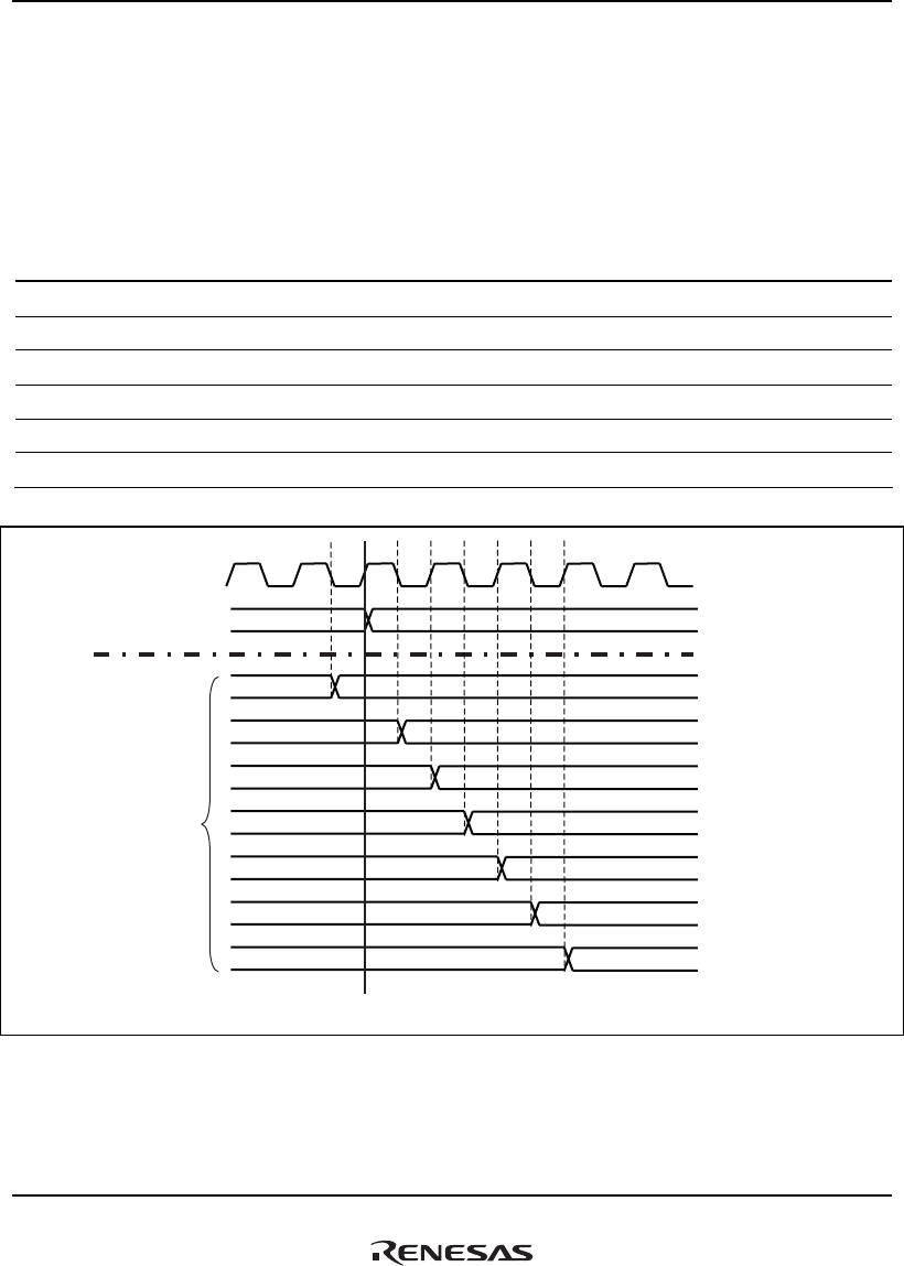
19. Display Unit (DU)
Rev.1.00 Jan. 10, 2008 Page 966 of 1658
REJ09B0261-0100
19.5.5 Output Signal Timing Adjustment
The display unit (DU) enables selection of output timing, with respect to the output dot clock, of
the various output signals (the four sync signals HSYNC, VSYNC, CSYNC, ODDF, as well as
DISP, CDE, CLAMP, DE, digital RGB signals). Timing is selected by setting OTAR.
Table 19.16 Output Signal Timing Setting Parameters
Bit Name in OTAR Description
SYNCA Sets output timing of the HSYNC, VSYNC, CSYNC, ODDF signal
DISPA Sets output timing of the DISP signal
CDEA Sets output timing of the CDE signal
DRGBA Sets output timing of digital RGB signal
CLAMPA Sets output timing of the CLAMP signal
DEA Sets output timing of the DE signal
DCLKOUT
Reference timing
Adjustable range of output timing
Register value
B'000
(Initial value)
B'100
B'101
B'001
B'110
B'010
B'111
B'011
Note: Timing charts other than this chart in this section are all provided on basic timing.
Figure 19.19 Adjustable Range of Output Timing
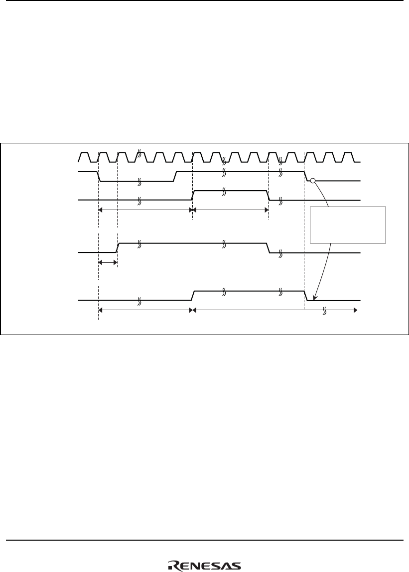
19. Display Unit (DU)
Rev.1.00 Jan. 10, 2008 Page 967 of 1658
REJ09B0261-0100
19.5.6 CLAMP Signal and DE Signal
The display unit (DU) generates a CLAMP signal and DE signal, independent of the DISP signal
indicating the display interval.
The rising-edge start position and high-level width of the CLAMP signal and DE signal, with
reference to the HSYNC signal falling edge, can be set in dot clock units. Figure 19.20 shows the
timing chart.
However, the DE signal is fixed at low level during the vertical blanking interval.
DCLKOUT
(output)
HSYNC signal
CLAMP signal/
DE signal
CLAMP signal/
DE signal
CLAMP signal/
DE signal
Starting position value
+ 1 High-level width value
The minimum value of rising position = 1
Start position value
+ 1
High-level width value
When the HSYNC
signal falls, the
CLAMP signal/DE
signal also falls.
When start position value is 0
When (start position value + high-level width value) exceeds the HSYNC period
Figure 19.20 CLAMP Signal and DE Signal

19. Display Unit (DU)
Rev.1.00 Jan. 10, 2008 Page 968 of 1658
REJ09B0261-0100
19.6 Power-Down Sequence
When executing the power-down sequence by the following modes or functions, turn off the
display in advance.
1. Sleep mode
2. Deep sleep mode
3. Module standby
4. Change of frequency
5. Manual reset
Even when the display unit (DU) enters the power-down sequence, the register values are retained.
During a power-down sequence, do not access the display unit (DU).
19.6.1 Procedures before Executing the Power-Down Sequence
1. Display is turned off by setting both the DEN and DRES bits in DSYSR to 0.
2. Use the VBK bit in DSSR to confirm the next VBK flag (because the display is turned off with
the timing of VBK).
3. The display unit (DU) displays the data in DOOR before the display is turned off.
4. Execute the power-down sequence.
5. Display unit (DU) is turned off.
19.6.2 Resetting the Power-Down Sequence
1. Reset the power-down sequence and start the clock.
2. Make settings to turn the display on, with the DEN and DRES bits in DSYSR set to 1 and 0
respectively.

20. Graphics Data Translation Accelerator (GDTA)
Rev.1.00 Jan. 10, 2008 Page 969 of 1658
REJ09B0261-0100
Section 20 Graphics Data Translation Accelerator (GDTA)
This block incorporates a YUV data conversion processing module (CL) that converts data in the
YUV 4:2:0 format to YUV 4:2:2 or ARGB format, as well as a video processing module (MC)
that generates estimated images using motion vectors.
A GADMAC is provided within the GDTA; the internal GADMAC performs high-speed data
transfer between external DDR2-SDRAM and the internal image processing function block,
bypassing the CPU. This block is also provided with buffer RAM; the buffer RAM is used for
color conversion table data in CL processing and as storage work RAM for IDCT data in MC
processing. RAM read access is performed by the internal GADMAC, to realize high-speed image
processing.
20.1 Features
• CL: YUV data conversion processing unit
Reads an image in external memory, processes the data, and writes the data back to external
memory
Conversion modes: YUV 4:2:0 → YUV 4:2:2 (YUYV mode), ARGB8888 (ARGB mode)
• MC: Video processing control unit
Reads images in external memory, processes the data, and writes the data back to external
memory
Generates estimated images through motion vectors in macroblock units (Y: 16 pixels x 16
lines, U/V: 8 pixels x 8 lines)
Modes: Forward, reverse, bidirectional, and intra macroblock processing
• Internal GADMAC dedicated to data transfer and internal data buffer RAM
The GADMAC for data transfer has four channels, and is capable of high-speed data transfer
bypassing the CPU.
In addition, 8 Kbytes of buffer RAM each are incorporated for both color conversion table data
storage in CL processing, and for IDCT data storage in MC processing.
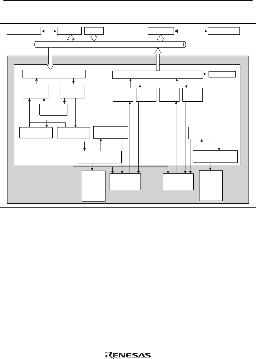
20. Graphics Data Translation Accelerator (GDTA)
Rev.1.00 Jan. 10, 2008 Page 970 of 1658
REJ09B0261-0100
Figure 20.1 shows the GDTA block diagram.
SuperHyway bus
External memory
Target interface Initiator interface
(external) (external)
Control
register
Buffer RAM
interface
RAM 0 interface
arbiter
CL/MC
interface
Buffer
RAM 0
(8 Kbytes)
Buffer
RAM 1
(8 Kbytes)
CL
function block
MC
function block
RAM 1 interface
arbiter
Request
queue
(4 planes)
Response
queue
(4 planes)
Color conversion
table control IDCT control
Arbiter
CPU
LBSC DDR2-SDRAMDDR2IF
CLW-
GADMAC
CLR-
GADMAC
MCW-
GADMAC
MCR-
GADMAC
GDTA
Figure 20.1 GDTA Block Diagram

20. Graphics Data Translation Accelerator (GDTA)
Rev.1.00 Jan. 10, 2008 Page 971 of 1658
REJ09B0261-0100
(1) Target Interface
The target interface controls access by the CPU to the GDTA internal registers, buffer RAM 0/1,
and CL and MC function blocks (image processing function blocks). The target interface places a
request queue/response queue in the high-speed SuperHyway bus reception unit, and alleviates the
access load of the initiator on this bus.
(2) Initiator Interface
Four GADMAC channels are provided within the GDTA, for data control during DMA data
transfer between external memory and internal image processing function blocks.
(3) GADMAC (CLR_GADMAC, CLW_GADMAC, MCR_GADMAC, MCW_GADMAC)
The GADMAC executes DMA control of data transfer between external memory and internal
image processing function blocks. A total of four channels are provided, including two channels
for CL functions and two channels for MC functions. The GADMAC is controlled through
registers within the CL function block and MC function block.
Applications of each of the channels are as follows.
CLR_GADMAC: Data transfer from external memory to the CL function block (read data
transfer)
CLW_GADMAC: Data transfer from the CL function block to external memory (write data
transfer)
MCR_GADMAC: Data transfer from external memory to the MC function block (read data
transfer)
MCW_GADMAC: Data transfer from the MC function block to external memory (write data
transfer)
* External memory: The external DDR2-SDRAM or the external memory connected to the
local bus.
(4) Color Conversion Table Control
In color conversion table control, color conversion table data is transferred between buffer RAM 0
and the CL function block.
(5) IDCT Control
In IDCT control, IDCT data is transferred between the buffer RAM 1 and MC function block.

20. Graphics Data Translation Accelerator (GDTA)
Rev.1.00 Jan. 10, 2008 Page 972 of 1658
REJ09B0261-0100
(6) Buffer RAM
Buffer RAM consists of two SRAM units each with an 8-Kbyte capacity. The RAM is used to
store color conversion table data for CL functions (buffer RAM 0) and to store IDCT data for MC
functions (buffer RAM 1). The entire 16-Kbyte capacity of this buffer RAM is allocated to a
memory map seen from the CPU. Valid access sizes are 4, 8, 16 and 32 bytes, and invalid access
sizes are 1 and 2 bytes.
(7) Buffer RAM Interface
The buffer RAM interface controls access to the buffer RAM 0/1. When there is access contention
between the CPU and the color conversion table transfer unit or the IDCT data transfer unit, bus
arbitration is performed. The buffer RAM interface exists as two independent blocks for the two
buffer RAM units. Because there is no access contention even during simultaneous reading of
buffer RAM 0 by the color conversion table data transfer unit and reading of buffer RAM 1 by the
IDCT table transfer unit, processing delays due to wait states and so on do not occur.
(8) CL Function Block
This block realizes CL functions. Specifically, data in YUV 4:2:0 format is converted into YUV
4:2:2 format or into ARGB8888 format.
(9) MC Function Block
This block realizes MC functions. Specifically, estimated images are generated using motion
vectors.
(10) CL/MC Bus Interface
The CL/MC bus interface controls access to the CL/MC function block by the CPU.
(11) Arbiter
When there is contention of access from each GADMAC in the GDTA to the SuperHyway bus,
bus arbitration is performed.
20. Graphics Data Translation Accelerator (GDTA)
Rev.1.00 Jan. 10, 2008 Page 973 of 1658
REJ09B0261-0100
20.2 GDTA Address Space
Figure 20.2 shows the GDTA address space (physical addresses). The GDTA consists of a number
of function blocks; the address space is divided into function block units owned by the respective
blocks. However, not all actually existing addresses are on the space; addresses following those in
a function block are mapped as mirror spaces for the function block. For the details of addresses
actually existing in each function block, refer to section 20.3, Register Descriptions. Mirror spaces
also exist in buffer RAM.
Note: The space from H'FE40_3000 to H'FE40_3FFF, excluding the space for registers
DRCL_CTL, DWCL_CTL, DRMC_CTL, DWMC_CTL, DCP_CTL, and DID_CTL is a
reserved area, and write access is prohibited. If write access is made, correct operation
cannot be guaranteed.
Common registers for bus interface
CL
MC
Buffer RAM 0 (8 Kbytes)
Buffer RAM 1 (8 Kbytes)
Reserved
Undefined (buffer RAM 0 mirror space: 8 Kbytes × 7)
Undefined (buffer RAM 1 mirror space: 8 Kbytes × 7)
Reserved
P4 area address Area 7 address
H'FE40 0000 H'1E40 0000
H'FE40 1000 H'1E40 1000
H'FE40 2000 H'1E40 2000
H'FE40 3000 H'1E40 3000
H'FE41 0000 H'1E41 0000
H'FE41 2000 H'1E41 2000
H'FE42 0000 H'1E42 0000
H'FE42 2000 H'1E42 2000
H'FE43 0000 H'1E43 0000
H'FE4F FFFF H'1E4F FFFF
Figure 20.2 GDTA Address Space Map (Physical Addresses)

20. Graphics Data Translation Accelerator (GDTA)
Rev.1.00 Jan. 10, 2008 Page 974 of 1658
REJ09B0261-0100
20.3 Register Descriptions
Table 20.1 to 20.3 show the register configuration of the GDTA. Table 20.4 to 20.6 show the
register states in each processing mode.
Table 20.1 GDTA Register Configuration (GDTA Common Registers)
Name Abbreviation R/W P4 Address
Area 7
Address
Access
Size
Sync
Clock
GA mask register GACMR R/W H'FE40 000C H'1E40 000C 32 GAck
GA enable register GACER R/W H'FE40 0010 H'1E40 0010 32 GAck
GA processing end
interrupt source
indicating register
GACISR R H'FE40 0014 H'1E40 0014 32 GAck
GA processing end
interrupt source
indication clear register
GACICR W H'FE40 0018 H'1E40 0018 32 GAck
GA interrupt enable
register
GACIER R/W H'FE40 001C H'1E40 001C 32 GAck
GA CL output data
alignment register
DWCL_CTL R/W H'FE40 3000 H'1E40 3000 32 GAck
GA CL input data
alignment register
DRCL_CTL R/W H'FE40 3200 H'1E40 3200 32 GAck
GA MC input data
alignment register
DRMC_CTL R/W H'FE40 3400 H'1E40 3400 32 GAck
GA MC output data
alignment register
DWMC_CTL R/W H'FE40 3600 H'1E40 3600 32 GAck
GA buffer RAM 0 data
alignment register
DCP_CTL R/W H'FE40 3800 H'1E40 3800 32 GAck
GA buffer RAM 1 data
alignment register
DID_CTL R/W H'FE40 3A00 H'1E40 3A00 32 GAck

20. Graphics Data Translation Accelerator (GDTA)
Rev.1.00 Jan. 10, 2008 Page 975 of 1658
REJ09B0261-0100
Table 20.2 GDTA Register Configuration (CL Block)
Name Abbreviation R/W P4 Address
Area 7
Address
Access
Size
Sync
Clock
CL command FIFO CLCF W H'FE40 1000 H'1E40 1000 32 GAck
CL control register CLCR R/W H'FE40 1004 H'1E40 1004 32 GAck
CL status register CLSR R H'FE40 1008 H'1E40 1008 32 GAck
CL frame width setting
register
CLWR R/W H'FE40 100C H'1E40 100C 32 GAck
CL frame height setting
register
CLHR R/W H'FE40 1010 H'1E40 1010 32 GAck
CL input Y padding size
setting register
CLIYPR R/W H'FE40 1014 H'1E40 1014 32 GAck
CL input UV padding
size setting register
CLIUVPR R/W H'FE40 1018 H'1E40 1018 32 GAck
CL output padding size
setting register
CLOPR R/W H'FE40 101C H'1E40 101C 32 GAck
CL palette pointer setting
register
CLPLPR R/W H'FE40 1020 H'1E40 1020 32 GAck

20. Graphics Data Translation Accelerator (GDTA)
Rev.1.00 Jan. 10, 2008 Page 976 of 1658
REJ09B0261-0100
Table 20.3 GDTA Register Configuration (MC Block)
Name Abbreviation R/W P4 Address
Area 7
Address
Access
Size
Sync
Clock
MC command FIFO MCCF W H'FE40 2000 H'1E40 2000 32 GAck
MC status register MCSR R H'FE40 2004 H'1E40 2004 32 GAck
MC frame width setting
register
MCWR R/W H'FE40 2008 H'1E40 2008 32 GAck
MC frame height setting
register
MCHR R/W H'FE40 200C H'1E40 200C 32 GAck
MC Y padding size
setting register
MCYPR R/W H'FE40 2010 H'1E40 2010 32 GAck
MC UV padding size
setting register
MCUVPR R/W H'FE40 2014 H'1E40 2014 32 GAck
MC output frame Y
pointer register
MCOYPR R/W H'FE40 2018 H'1E40 2018 32 GAck
MC output frame U
pointer register
MCOUPR R/W H'FE40 201C H'1E40 201C 32 GAck
MC output frame V
pointer register
MCOVPR R/W H'FE40 2020 H'1E40 2020 32 GAck
MC past frame Y pointer
register
MCPYPR R/W H'FE40 2024 H'1E40 2024 32 GAck
MC past frame U pointer
register
MCPUPR R/W H'FE40 2028 H'1E40 2028 32 GAck
MC past frame V pointer
register
MCPVPR R/W H'FE40 202C H'1E40 202C 32 GAck
MC future frame Y
pointer register
MCFYPR R/W H'FE40 2030 H'1E40 2030 32 GAck
MC future frame U
pointer register
MCFUPR R/W H'FE40 2034 H'1E40 2034 32 GAck
MC future frame V
pointer register
MCFVPR R/W H'FE40 2038 H'1E40 2038 32 GAck

20. Graphics Data Translation Accelerator (GDTA)
Rev.1.00 Jan. 10, 2008 Page 977 of 1658
REJ09B0261-0100
Table 20.4 GDTA Register States in Each Processing Mode (GDTA Common Registers)
Register
Abbreviation Power-On Reset Manual Reset Sleep Deep Sleep
GACMR H'0000 0000 H'0000 0000 Retained Retained
GACER H'0000 0000 H'0000 0000 Retained Retained
GACISR H'0000 0000 H'0000 0000 Retained Retained
GACICR H'0000 0000 H'0000 0000 Retained Retained
GACIER H'0000 0000 H'0000 0000 Retained Retained
DWCL_CTL H'0000 0000 H'0000 0000 Retained Retained
DRCL_CTL H'0000 0000 H'0000 0000 Retained Retained
DRMC_CTL H'0000 0000 H'0000 0000 Retained Retained
DWMC_CTL H'0000 0000 H'0000 0000 Retained Retained
DCP_CTL H'0000 0000 H'0000 0000 Retained Retained
DID_CTL H'0000 0000 H'0000 0000 Retained Retained
Table 20.5 GDTA States in Each Processing Mode (CL Block)
Register
Abbreviation Power-On Reset Manual Reset Sleep Deep Sleep
CLCF H'0000 0000 H'0000 0000 Retained H'0000_0000
CLCR H'0000 0000 H'0000 0000 Retained Retained
CLSR H'0000 0000 H'0000 0000 Retained Retained
CLWR H'0000 0000 H'0000 0000 Retained Retained
CLHR H'0000 0000 H'0000 0000 Retained Retained
CLIYPR H'0000 0000 H'0000 0000 Retained Retained
CLIUVPR H'0000 0000 H'0000 0000 Retained Retained
CLOPR H'0000 0000 H'0000 0000 Retained Retained
CLPLPR H'0000 0000 H'0000 0000 Retained Retained
Note: A 0 is always read from these registers.

20. Graphics Data Translation Accelerator (GDTA)
Rev.1.00 Jan. 10, 2008 Page 978 of 1658
REJ09B0261-0100
Table 20.6 GDTA States in Each Processing Mode (MC Block)
Register
Abbreviation
Power-On
Reset Manual Reset Sleep Deep Sleep
Module
Standby
MCCF H'0000 0000 H'0000 0000 Retained H'0000_0000 H'0000_0000
MCSR H'0000 0000 H'0000 0000 Retained Retained Retained
MCWR H'0000 0000 H'0000 0000 Retained Retained Retained
MCHR H'0000 0000 H'0000 0000 Retained Retained Retained
MCYPR H'0000 0000 H'0000 0000 Retained Retained Retained
MCUVPR H'0000 0000 H'0000 0000 Retained Retained Retained
MCOYPR H'0000 0000 H'0000 0000 Retained Retained Retained
MCOUPR H'0000 0000 H'0000 0000 Retained Retained Retained
MCOVPR H'0000 0000 H'0000 0000 Retained Retained Retained
MCPYPR H'0000 0000 H'0000 0000 Retained Retained Retained
MCPUPR H'0000 0000 H'0000 0000 Retained Retained Retained
MCPVPR H'0000 0000 H'0000 0000 Retained Retained Retained
MCFYPR H'0000 0000 H'0000 0000 Retained Retained Retained
MCFUPR H'0000 0000 H'0000 0000 Retained Retained Retained
MCFVPR H'0000 0000 H'0000 0000 Retained Retained Retained
Note: A 0 is always read from these registers.

20. Graphics Data Translation Accelerator (GDTA)
Rev.1.00 Jan. 10, 2008 Page 979 of 1658
REJ09B0261-0100
20.3.1 GA Mask Register (GACMR)
GACMR is in the GDTA common register block and enables writing to the GA enable register
(GACER). Writing to GACER is enabled by writing of the key code to this register. In the initial
state, the key code is not written and writing to GACER is disabled.
161718192021222324252627282931 30
0000000000000000
GACM
R/WR/WR/WR/WR/WR/WR/WR/WR/WR/WR/WR/WR/WR/WR/W R/W
BIt:
Initial value:
R/W:
01234567891011121315 14
0000000000000000
GACM
R/WR/WR/WR/WR/WR/WR/WR/WR/WR/WR/WR/WR/WR/WR/W R/W
BIt:
Initial value:
R/W:
Bit Bit Name
Initial
Value R/W Description
31 to 0 GACM 0 R/W Write the key code [H'A55A 0FF0] to enable writing to
GACER. If a value other than the key code is written,
writing to the GA enable register is disabled.

20. Graphics Data Translation Accelerator (GDTA)
Rev.1.00 Jan. 10, 2008 Page 980 of 1658
REJ09B0261-0100
20.3.2 GA Enable Register (GACER)
GACER is in the GDTA common register block and controls the block operation.
161718192021222324252627282931 30
0000000000000000
⎯⎯⎯⎯⎯⎯⎯⎯⎯⎯⎯⎯⎯⎯⎯⎯
⎯⎯⎯⎯⎯⎯⎯⎯⎯⎯⎯⎯⎯⎯⎯⎯
BIt:
Initial value:
R/W:
01234567891011121315 14
0000000000000000
CL_ENMC_EN
⎯⎯⎯⎯⎯⎯⎯⎯⎯⎯⎯⎯⎯⎯
R/WR/W⎯⎯⎯⎯⎯⎯⎯⎯⎯⎯⎯⎯⎯⎯
BIt:
Initial value:
R/W:
Bit Bit Name
Initial
Value R/W Description
31 to 2 ⎯ All 0 ⎯ Reserved
These bits are always read as 0. The write value should
always be 0.
1 MC_EN 0 R/W Enables access to the MC registers.
0: Writing to the MC registers is invalid. The value read
from the MC register is undefined.
1: Reading and writing are enabled.
0 CL_EN 0 R/W Enables access to the CL registers.
0: Writing to the CL registers is invalid. The value read
from the CL register is undefined.
1: Reading and writing are enabled.

20. Graphics Data Translation Accelerator (GDTA)
Rev.1.00 Jan. 10, 2008 Page 981 of 1658
REJ09B0261-0100
20.3.3 GA Interrupt Source Indicating Register (GACISR)
GACISR is in the GDTA common register block and indicates the states of interrupt sources for
each module.
161718192021222324252627282931 30
0000000000000000
⎯⎯⎯⎯⎯⎯⎯⎯⎯⎯⎯⎯⎯⎯⎯⎯
⎯⎯⎯⎯⎯⎯⎯⎯⎯⎯⎯⎯⎯⎯⎯⎯
BIt:
Initial value:
R/W:
01234567891011121315 14
0000000000000000
CL_ENDMC_ENDCL_ERRMC_ERR
⎯⎯⎯⎯⎯⎯⎯⎯⎯⎯⎯⎯
RRRR⎯⎯⎯⎯⎯⎯⎯⎯⎯⎯⎯⎯
BIt:
Initial value:
R/W:
Bit Bit Name
Initial
Value R/W Description
31 to 4 ⎯ All 0 ⎯ Reserved
These bits are always read as 0. The write value should
always be 0.
3 MC_EER 0 R Indicates whether an MC module error interrupt has
occurred.
0: No error
1: Error occurred
2 CL_EER 0 R Indicates whether a CL module error interrupt has
occurred.
0: No error
1: Error occurred
1 MC_END 0 R Indicates whether an MC module processing end
interrupt has occurred.
0: '1' has been written to the MC_ENCR bit in GACICR.
1: Processing completed
0 CL_END 0 R Indicates whether a CL module processing end interrupt
has occurred.
0: '1' has been written to the CL_ENCR bit in GACICR.
1: Processing completed
Note: MC processing completion is indicated when the command processing is complete and the
end command is written to the MC command FIFO (see section 20.3.17, CL Input Y
Padding Size Setting Register (CLIYPR)).

20. Graphics Data Translation Accelerator (GDTA)
Rev.1.00 Jan. 10, 2008 Page 982 of 1658
REJ09B0261-0100
20.3.4 GA Interrupt Source Indication Clear Register (GACICR)
GACICR is in the GDTA common register block and clears interrupt source indication for each
module. Bits in this register are read as 0.
161718192021222324252627282931 30
0000000000000000
⎯⎯⎯⎯⎯⎯⎯⎯⎯⎯⎯⎯⎯⎯⎯⎯
⎯⎯⎯⎯⎯⎯⎯⎯⎯⎯⎯⎯⎯⎯⎯⎯
BIt:
Initial value:
R/W:
01234567891011121315 14
0000000000000000
CL_
ENCR
MC_
ENCR
CL_
ERCR
MC_
ERCR
⎯⎯⎯⎯⎯⎯⎯⎯⎯⎯⎯⎯
WWWW⎯⎯⎯⎯⎯⎯⎯⎯⎯⎯⎯⎯
BIt:
Initial value:
R/W:
Bit Bit Name
Initial
Value R/W Description
31 to 4 ⎯ All 0 ⎯ Reserved
These bits are always read as 0. The write value should
always be 0.
3 MC_ERCR 0 W Clears indication of an MC error interrupt (clears the
MC_ERR bit)
0: No effect
1: Clears error interrupt indication
2 CL_ERCR 0 W Clears indication of a CL error interrupt (clears the
CL_ERR bit)
0: No effect
1: Clears error interrupt indication
1 MC_ENCR 0 W Clears indication of an MC processing end interrupt
(clears the MC_END bit)
0: No effect
1: Clears processing end interrupt indication
0 CL_ENCR 0 W Clears indication of a CL processing end interrupt (clears
the CL_END bit)
0: No effect
1: Clears processing end interrupt indication

20. Graphics Data Translation Accelerator (GDTA)
Rev.1.00 Jan. 10, 2008 Page 983 of 1658
REJ09B0261-0100
20.3.5 GA Interrupt Enable Register (GACIER)
GACIER is in the GDTA common register block and sets interrupt output for each module.
161718192021222324252627282931 30
0000000000000000
⎯⎯⎯⎯⎯⎯⎯⎯⎯⎯⎯⎯⎯⎯⎯⎯
⎯⎯⎯⎯⎯⎯⎯⎯⎯⎯⎯⎯⎯⎯⎯⎯
BIt:
Initial value:
R/W:
01234567891011121315 14
0000000000000000
CL_
ENEN
MC_
ENEN
CL_
EREN
MC_
EREN
⎯⎯⎯⎯⎯⎯⎯⎯⎯⎯⎯⎯
R/WR/WR/WR/W⎯⎯⎯⎯⎯⎯⎯⎯⎯⎯⎯⎯
BIt:
Initial value:
R/W:
Bit Bit Name
Initial
Value R/W Description
31 to 4 ⎯ All 0 ⎯ Reserved
These bits are always read as 0. The write value should
always be 0.
3 MC_EREN 0 R/W Controls output of an MC module error interrupt
0: Does not output the interrupt.
1: Outputs the interrupt.
2 CL_EREN 0 R/W Controls output of a CL module error interrupt
0: Does not output the interrupt.
1: Outputs the interrupt.
1 MC_ENEN 0 R/W Controls output of an MC module processing end
interrupt
0: Does not output the interrupt.
1: Outputs the interrupt.
0 CL_ENEN 0 R/W Controls output of a CL module processing end interrupt
0: Does not output the interrupt.
1: Outputs the interrupt.

20. Graphics Data Translation Accelerator (GDTA)
Rev.1.00 Jan. 10, 2008 Page 984 of 1658
REJ09B0261-0100
20.3.6 GA CL Input Data Alignment Register (DRCL_CTL)
DRCL_CTL is in the GDTA common register block and specifies data alignment of CL input
data.
161718192021222324252627282931 30
0000000000000000
⎯⎯⎯⎯⎯⎯⎯⎯⎯⎯⎯⎯⎯⎯⎯⎯
⎯⎯⎯⎯⎯⎯⎯⎯⎯⎯⎯⎯⎯⎯⎯⎯
BIt:
Initial value:
R/W:
01234567891011121315 14
0000000000000000
DCLR_DTUADCLR_DTSA
DCLR_
DTAM
⎯⎯⎯⎯⎯⎯⎯⎯⎯⎯⎯
R/WR/WR/WR/WR/W⎯⎯⎯⎯⎯⎯⎯⎯⎯⎯⎯
BIt:
Initial value:
R/W:
Bit Bit Name
Initial
Value R/W Description
31 to 5 ⎯ All 0 ⎯ Reserved
These bits are always read as 0. The write value should
always be 0.
4 DCLR_DTAM 0 R/W Specifies data alignment conversion mode.
0: Data alignment is performed using an endian signal
1: Data alignment is performed using the DRCL_CTL
register setting
3, 2 DCLR_DTSA 0 R/W Specifies the data size for data alignment conversion.
00: No conversion
01: 64 bits
10: 32 bits
11: 16 bits
1, 0 DCLR_DTUA 0 R/W Specifies the unit for data alignment conversion.
00: No conversion
01: 8 bits
10: 16 bits
11: 32 bits
Note: For details of data alignment conversion patterns, refer to section 20.6, Data Alignment.

20. Graphics Data Translation Accelerator (GDTA)
Rev.1.00 Jan. 10, 2008 Page 985 of 1658
REJ09B0261-0100
20.3.7 GA CL Output Data Alignment Register (DWCL_CTL)
DWCL_CTL is in the GDTA common register block and specifies data alignment of CL output
data.
161718192021222324252627282931 30
0000000000000000
⎯⎯⎯⎯⎯⎯⎯⎯⎯⎯⎯⎯⎯⎯⎯⎯
⎯⎯⎯⎯⎯⎯⎯⎯⎯⎯⎯⎯⎯⎯⎯⎯
BIt:
Initial value:
R/W:
01234567891011121315 14
0000000000000000
DCLW_DTUADCLW_DTSA
DCLW_
DTAM
⎯⎯⎯⎯⎯⎯⎯⎯⎯⎯⎯
R/WR/WR/WR/WR/W⎯⎯⎯⎯⎯⎯⎯⎯⎯⎯⎯
BIt:
Initial value:
R/W:
Bit Bit Name
Initial
Value R/W Description
31 to 5 ⎯ All 0 ⎯ Reserved
These bits are always read as 0. The write value should
always be 0.
4 DCLW_DTAM 0 R/W Specifies data alignment conversion mode
0: Data alignment is performed using an endian signal
1: Data alignment is performed using the DWCL_CTL
register setting
3, 2 DCLW_DTSA 0 R/W Specifies the data size for data alignment conversion.
00: No conversion
01: 64 bits
10: 32 bits
11: 16 bits
1, 0 DCLW_DTUA 0 R/W Specifies the unit for data alignment conversion.
00: No conversion
01: 8 bits
10: 16 bits
11: 32 bits
Note: For details of data alignment conversion patterns, refer to section 20.6, Data Alignment.

20. Graphics Data Translation Accelerator (GDTA)
Rev.1.00 Jan. 10, 2008 Page 986 of 1658
REJ09B0261-0100
20.3.8 GA MC Input Data Alignment Register (DRMC_CTL)
DRMC_CTL is in the GDTA common register block and specifies data alignment of MC input
data.
161718192021222324252627282931 30
0000000000000000
⎯⎯⎯⎯⎯⎯⎯⎯⎯⎯⎯⎯⎯⎯⎯⎯
⎯⎯⎯⎯⎯⎯⎯⎯⎯⎯⎯⎯⎯⎯⎯⎯
BIt:
Initial value:
R/W:
01234567891011121315 14
0000000000000000
DMCR_DTUADMCR_DTSA
DMCR_
DTAM
⎯⎯⎯⎯⎯⎯⎯⎯⎯⎯⎯
R/WR/WR/WR/WR/W⎯⎯⎯⎯⎯⎯⎯⎯⎯⎯⎯
BIt:
Initial value:
R/W:
Bit Bit Name
Initial
Value R/W Description
31 to 5 ⎯ All 0 ⎯ Reserved
These bits are always read as 0. The write value should
always be 0.
4 DMCR_DTAM 0 R/W Specifies data alignment conversion mode
0: Data alignment is performed using an endian signal
1: Data alignment is performed using the DRMC_CTL
register setting
3, 2 DMCR_DTSA 0 R/W Specifies the data size for data alignment conversion.
00: No conversion
01: 64 bits
10: 32 bits
11: 16 bits
1, 0 DMCR_DTUA 0 R/W Specifies the unit for data alignment conversion.
00: No conversion
01: 8 bits
10: 16 bits
11: 32 bits
Note: For details of data alignment conversion patterns, refer to section 20.6, Data Alignment.

20. Graphics Data Translation Accelerator (GDTA)
Rev.1.00 Jan. 10, 2008 Page 987 of 1658
REJ09B0261-0100
20.3.9 GA MC Output Data Alignment Register (DWMC_CTL)
DWMC_CTL is in the GDTA common register block and specifies data alignment of MC output
data.
161718192021222324252627282931 30
0000000000000000
⎯⎯⎯⎯⎯⎯⎯⎯⎯⎯⎯⎯⎯⎯⎯⎯
⎯⎯⎯⎯⎯⎯⎯⎯⎯⎯⎯⎯⎯⎯⎯⎯
BIt:
Initial value:
R/W:
01234567891011121315 14
0000000000000000
DMCW_DTUADMCW_DTSA
DMCW_
DTAM
⎯⎯⎯⎯⎯⎯⎯⎯⎯⎯⎯
R/WR/WR/WR/WR/W⎯⎯⎯⎯⎯⎯⎯⎯⎯⎯⎯
BIt:
Initial value:
R/W:
Bit Bit Name
Initial
Value R/W Description
31 to 5 ⎯ All 0 ⎯ Reserved
These bits are always read as 0. The write value should
always be 0.
4 DMCW_DTAM 0 R/W Specifies data alignment conversion mode
0: Data alignment is performed using an endian signal
1: Data alignment is performed using the DWMC_CTL
register setting
3, 2 DMCW_DTSA 0 R/W Specifies the data size for data alignment conversion.
00: No conversion
01: 64 bits
10: 32 bits
11: 16 bits
1, 0 DMCW_DTUA 0 R/W Specifies the unit for data alignment conversion.
00: No conversion
01: 8 bits
10: 16 bits
11: 32 bits
Note: For details of data alignment conversion patterns, refer to section 20.6, Data Alignment.

20. Graphics Data Translation Accelerator (GDTA)
Rev.1.00 Jan. 10, 2008 Page 988 of 1658
REJ09B0261-0100
20.3.10 GA Buffer RAM 0 Data Alignment Register (DCP_CTL)
DCP_CTL is in the GDTA common register block and specifies data alignment of the data stored
in buffer RAM 0.
161718192021222324252627282931 30
0000000000000000
⎯⎯⎯⎯⎯⎯⎯⎯⎯⎯⎯⎯⎯⎯⎯⎯
⎯⎯⎯⎯⎯⎯⎯⎯⎯⎯⎯⎯⎯⎯⎯⎯
BIt:
Initial value:
R/W:
01234567891011121315 14
0000000000000000
DCP_DTUADCP_DTSA
DCP_
DTAM
⎯⎯⎯⎯⎯⎯⎯⎯⎯⎯⎯
R/WR/WR/WR/WR/W⎯⎯⎯⎯⎯⎯⎯⎯⎯⎯⎯
BIt:
Initial value:
R/W:
Bit Bit Name
Initial
Value R/W Description
31 to 5 ⎯ All 0 ⎯ Reserved
These bits are always read as 0. The write value should
always be 0.
4 DCP_DTAM 0 R/W Specifies data alignment conversion mode
0: Data alignment is performed using an endian signal
1: Data alignment is performed using the DCP_CTL
register setting
3, 2 DCP_DTSA 0 R/W Specifies the data size for data alignment conversion.
00: No conversion
01: 64 bits
10: 32 bits
11: 16 bits
1, 0 DCP_DTUA 0 R/W Specifies the unit for data alignment conversion.
00: No conversion
01: 8 bits
10: 16 bits
11: 32 bits
Note: For details of data alignment conversion patterns, refer to section 20.6, Data Alignment.

20. Graphics Data Translation Accelerator (GDTA)
Rev.1.00 Jan. 10, 2008 Page 989 of 1658
REJ09B0261-0100
20.3.11 GA Buffer RAM 1 Data Alignment Register (DID_CTL)
DID_CTL is in the GDTA common register block and specifies data alignment of the data stored
in buffer RAM 1.
161718192021222324252627282931 30
0000000000000000
⎯⎯⎯⎯⎯⎯⎯⎯⎯⎯⎯⎯⎯⎯⎯⎯
⎯⎯⎯⎯⎯⎯⎯⎯⎯⎯⎯⎯⎯⎯⎯⎯
BIt:
Initial value:
R/W:
01234567891011121315 14
0000000000000000
DID_DTUADID_DTSA
DID_
DTAM
⎯⎯⎯⎯⎯⎯⎯⎯⎯⎯⎯
R/WR/WR/WR/WR/W⎯⎯⎯⎯⎯⎯⎯⎯⎯⎯⎯
BIt:
Initial value:
R/W:
Bit Bit Name
Initial
Value R/W Description
31 to 5 ⎯ All 0 ⎯ Reserved
These bits are always read as 0. The write value should
always be 0.
4 DID_DTAM 0 R/W Specifies data alignment conversion mode
0: Data alignment is performed using an endian signal
1: Data alignment is performed using the DID_CTL
register setting
3, 2 DID_DTSA 0 R/W Specifies the data size for data alignment conversion.
00: No conversion
01: 64 bits
10: 32 bits
11: 16 bits
1, 0 DID_DTUA 0 R/W Specifies the unit for data alignment conversion.
00: No conversion
01: 8 bits
10: 16 bits
11: 32 bits
Note: For details of data alignment conversion patterns, refer to section 20.6, Data Alignment.
20. Graphics Data Translation Accelerator (GDTA)
Rev.1.00 Jan. 10, 2008 Page 990 of 1658
REJ09B0261-0100
20.3.12 CL Command FIFO (CLCF)
CLCF is in the CL register block and receives commands. This register uses the FIFO method and
recognizes four command parameters according to the writing order. This register does not retain
the written values. This register is always read as 0.
161718192021222324252627282931 30
0000000000000000
CL_CF
WWWWWWWWWWWWWWWW
BIt:
Initial value:
R/W:
01234567891011121315 14
0000000000000000
CL_CF
WWWWWWWWWWWWWWWW
BIt:
Initial value:
R/W:
Bit Bit Name
Initial
Value R/W Description
31 to 0 CL_CF 0 W Command FIFO register
Notes: 1. Setting Method
When accessing this register, the CL_EN bit in GACER should be set to 1. Access is
possible only when the CL_EN bit is set to 1. If the CL_EN bit is 0, access is invalid
(writing is invalid; the result of reading is indefinite).
The following shows the parameter contents assumed according to the writing order:
Writing Order Setting Contents
CL command parameter 1 Input Y pointer
CL command parameter 2 Input U pointer
CL command parameter 3 Input V pointer CL command
CL command parameter 4 Output pointer
• Input Y pointer: Pointer for input Y data (Input Y data storing address)
• Input U pointer: Pointer for input U data (Input U data storing address)
• Input V pointer: Pointer for input V data (Input V data storing address)
• Output pointer: Pointer for output data (Output data storing address)

20. Graphics Data Translation Accelerator (GDTA)
Rev.1.00 Jan. 10, 2008 Page 991 of 1658
REJ09B0261-0100
2. Setting Method When Setting Values in Succession
When setting values in this register in succession, the CL module is able to receive the
next command while the CL_CFF bit in CLSR is 0. To perform processing by changing
the command alone, just set the new command in this register.
3. The input Y/U/V pointers and output pointers must be set to point to addresses on 32-
byte boundaries. If not, the lower address is regarded as 0.
4. Two commands can be received. If the next command is written when the command
FIFO is full, the commands stored in the command FIFO are retained and the next
command is ignored.
20.3.13 CL Control Register (CLCR)
CLCR is in the CL register block and specifies the CL operating mode.
161718192021222324252627282931 30
0000000000000000
⎯⎯⎯⎯⎯⎯⎯⎯⎯⎯⎯⎯⎯⎯⎯⎯
⎯⎯⎯⎯⎯⎯⎯⎯⎯⎯⎯⎯⎯⎯⎯⎯
BIt:
Initial value:
R/W:
01234567891011121315 14
0000000000000000
CL_MDCL_OACL_OD⎯CL_DA⎯⎯⎯⎯⎯⎯⎯
R/WR/WR/W⎯R/WR/WR/WR/WR/W⎯⎯⎯⎯⎯⎯⎯
BIt:
Initial value:
R/W:
Bit Bit Name
Initial
Value R/W Description
31 to 9 ⎯ All 0 ⎯ Reserved
These bits are always read as 0. The write value should
always be 0.
8 to 4 CL_DA All 0 R/W Specifies output data alignment.
The correspondence between the alignment and
specified value is shown in the following table.
3 ⎯ 0 ⎯ Reserved
This bit is always read as 0. The write value should
always be 0.
2 CL_OD 0 R/W Specifies output access size (access size for output)
0: 4 bytes
1: 32 bytes

20. Graphics Data Translation Accelerator (GDTA)
Rev.1.00 Jan. 10, 2008 Page 992 of 1658
REJ09B0261-0100
Bit Bit Name
Initial
Value R/W Description
1 CL_OA 0 R/W Specifies output address mode
0: Output address incremented
When the output access size is 4 bytes, the address is
incremented by H'4; when the output access size is 32
bytes, the address is incremented by H'20.
1: Output address fixed
The address set in CLCF as command parameter 4
(output pointer) is output.
0 CL_MD 0 R/W Specifies conversion mode
0: YUYV conversion
Converts from YUV420 to YUV422 format
1: ARGB conversion
Converts from YUV420 to ARGB8888 format
A Table of CL_DA Register Settings And Output Data Alignment
CL_DA
YUYV
Conversion
ARGB
Conversion CL_DA
YUYV
Conversion
ARGB
Conversion
H'0 Y0UY1V ARGB H'10 UVY0Y1 RBAG
H'1 Y0UVY1 ARBG H'11 UVY1Y0 RBGA
H'2 Y0Y1UV AGRB H'12 VY1Y0U BGAR
H'3 Y0Y1VU AGBR H'13 VY1UY0 BGRA
H'4 Y0VY1U ABGR H'14 VY0Y1U BAGR
H'5 Y0VUY1 ABRG H'15 VY0UY1 BARG
H'6 Y1UY0V GRAB H'16 VUY0Y1 BRAG
H'7 Y1UVY0 GRBA H'17 VUY1Y0 BRGA
H'8 Y1Y0UV GARB H'18 Y0UY1V ARGB
H'9 Y1Y0VU GABR H'19 Y0UY1V ARGB
H'A Y1VY0U GBAR H'1A Y0UY1V ARGB
H'B Y1VUY0 GBRA H'1B Y0UY1V ARGB
H'C UY1Y0V RGAB H'1C Y0UY1V ARGB
H'D UY1VY0 RGBA H'1D Y0UY1V ARGB
H'E UY0Y1V RAGB H'1E Y0UY1V ARGB
H'F UY0VY1 RABG H'1F Y0UY1V ARGB

20. Graphics Data Translation Accelerator (GDTA)
Rev.1.00 Jan. 10, 2008 Page 993 of 1658
REJ09B0261-0100
20.3.14 CL Status Register (CLSR)
CLSR is in the CL register block and indicates the internal states of the CL.
161718192021222324252627282931 30
0000000000000000
⎯⎯⎯⎯⎯⎯⎯⎯⎯⎯⎯⎯⎯⎯⎯⎯
⎯⎯⎯⎯⎯⎯⎯⎯⎯⎯⎯⎯⎯⎯⎯⎯
BIt:
Initial value:
R/W:
01234567891011121315 14
0000000000000000
CL_CFSCL_CFF
CLSR_
EXE
⎯⎯⎯⎯⎯⎯⎯⎯⎯⎯⎯⎯
RRRR⎯⎯⎯⎯⎯⎯⎯⎯⎯⎯⎯⎯
BIt:
Initial value:
R/W:
Bit Bit Name
Initial
Value R/W Description
31 to 4 ⎯ All 0 ⎯ Reserved
These bits are always read as 0. The write value should
always be 0.
3 CLSR_EXE 0 R CL execution state display
0: Stopped
1: Executing
2 CL_CFF 0 R CL_CF (command FIFO) status display
Indicates the state of command buffer reception.
0: Command receivable
1: Command buffer full
1, 0 CL_CFS 0 R Command pointer status display
00: CL_CF command parameter 1 setting wait state
01: CL_CF command parameter 2 setting wait state
10: CL_CF command parameter 3 setting wait state
11: CL_CF command parameter 4 setting wait state

20. Graphics Data Translation Accelerator (GDTA)
Rev.1.00 Jan. 10, 2008 Page 994 of 1658
REJ09B0261-0100
20.3.15 CL Frame Width Setting Register (CLWR)
CLWR is in the CL register block and sets the input image width in pixel units.
161718192021222324252627282931 30
0000000000000000
⎯⎯⎯⎯⎯⎯⎯⎯⎯⎯⎯⎯⎯⎯⎯⎯
⎯⎯⎯⎯⎯⎯⎯⎯⎯⎯⎯⎯⎯⎯⎯⎯
BIt:
Initial value:
R/W:
01234567891011121315 14
0000000000000000
CL_W
⎯⎯⎯⎯
R/WR/WR/WR/WR/WR/WR/WR/WR/WR/WR/WR/W⎯⎯⎯⎯
BIt:
Initial value:
R/W:
Bit Bit Name
Initial
Value R/W Description
31 to 12 ⎯ All 0 ⎯ Reserved
These bits are always read as 0. The write value should
always be 0.
11 to 0 CL_W All 0 R/W Frame width setting
Should be set in pixel units.
Value set should be 2 × n (n: an integer greater than 0)
Notes: 1. CL processing is prohibited when the setting is 0.
2. Addition is performed taking that 1 pixel = 1 byte.
3. CLWR (bytes) + CLIYPR (bytes) should be 32 bytes × n (n: an integer greater than 0)
4. CLWR (bytes)/2 + CLUVPR (bytes) should be 32 bytes × n (n: an integer greater than
0)

20. Graphics Data Translation Accelerator (GDTA)
Rev.1.00 Jan. 10, 2008 Page 995 of 1658
REJ09B0261-0100
20.3.16 CL Frame Height Setting Register (CLHR)
CLHR is in the CL register block and sets the input image height in line units.
161718192021222324252627282931 30
0000000000000000
⎯⎯⎯⎯⎯⎯⎯⎯⎯⎯⎯⎯⎯⎯⎯⎯
⎯⎯⎯⎯⎯⎯⎯⎯⎯⎯⎯⎯⎯⎯⎯⎯
BIt:
Initial value:
R/W:
01234567891011121315 14
0000000000000000
CL_H
⎯⎯⎯⎯
R/WR/WR/WR/WR/WR/WR/WR/WR/WR/WR/WR/W⎯⎯⎯⎯
BIt:
Initial value:
R/W:
Bit Bit Name
Initial
Value R/W Description
31 to 12 ⎯ All 0 ⎯ Reserved
These bits are always read as 0. The write value should
always be 0.
11 to 0 CL_H All 0 R/W Frame height setting
Should be set in line units.
Note: CL processing is prohibited when the setting is 0.

20. Graphics Data Translation Accelerator (GDTA)
Rev.1.00 Jan. 10, 2008 Page 996 of 1658
REJ09B0261-0100
20.3.17 CL Input Y Padding Size Setting Register (CLIYPR)
CLIYPR is in the CL register block and sets the input Y padding size in byte units.
161718192021222324252627282931 30
0000000000000000
⎯⎯⎯⎯⎯⎯⎯⎯⎯⎯⎯⎯⎯⎯⎯⎯
⎯⎯⎯⎯⎯⎯⎯⎯⎯⎯⎯⎯⎯⎯⎯⎯
BIt:
Initial value:
R/W:
01234567891011121315 14
0000000000000000
CL_IYP
⎯⎯⎯⎯
R/WR/WR/WR/WR/WR/WR/WR/WR/WR/WR/WR/W⎯⎯⎯⎯
BIt:
Initial value:
R/W:
Bit Bit Name
Initial
Value R/W Description
31 to 12 ⎯ All 0 ⎯ Reserved
These bits are always read as 0. The write value should
always be 0.
11 to 0 CL_IYP All 0 R/W Input Y padding size setting
Should be set in byte units.
Value set should be 2 × n (n: an integer greater than 0)
Notes: 1. Addition is performed taking that 1 pixel = 1 byte.
2. CLWR (bytes) + CLIYPR (bytes) should be 32 bytes × n (n: an integer greater than 0)

20. Graphics Data Translation Accelerator (GDTA)
Rev.1.00 Jan. 10, 2008 Page 997 of 1658
REJ09B0261-0100
20.3.18 CL Input UV Padding Size Setting Register (CLIUVPR)
CLIUVPR is in the CL register block and sets the input UV padding size in byte units.
161718192021222324252627282931 30
0000000000000000
⎯⎯⎯⎯⎯⎯⎯⎯⎯⎯⎯⎯⎯⎯⎯⎯
⎯⎯⎯⎯⎯⎯⎯⎯⎯⎯⎯⎯⎯⎯⎯⎯
BIt:
Initial value:
R/W:
01234567891011121315 14
0000000000000000
CL_IUVP
⎯⎯⎯⎯
R/WR/WR/WR/WR/WR/WR/WR/WR/WR/WR/WR/W⎯⎯⎯⎯
BIt:
Initial value:
R/W:
Bit Bit Name
Initial
Value R/W Description
31 to 12 ⎯ All 0 ⎯ Reserved
These bits are always read as 0. The write value should
always be 0.
11 to 0 CL_IUVP All 0 R/W Input UV padding size setting
Should be set in byte units.
Notes: 1. Addition is performed taking that 1 pixel = 1 byte.
2. CLWR (bytes)/2 + CLUVPR (bytes) should be 32 bytes × n (n: an integer greater than
0)

20. Graphics Data Translation Accelerator (GDTA)
Rev.1.00 Jan. 10, 2008 Page 998 of 1658
REJ09B0261-0100
20.3.19 CL Output Padding Size Setting Register (CLOPR)
CLOPR is in the CL register block and sets the output padding size in byte units.
161718192021222324252627282931 30
0000000000000000
⎯⎯⎯⎯⎯⎯⎯⎯⎯⎯⎯⎯⎯⎯⎯⎯
⎯⎯⎯⎯⎯⎯⎯⎯⎯⎯⎯⎯⎯⎯⎯⎯
BIt:
Initial value:
R/W:
01234567891011121315 14
0000000000000000
CL_OP
⎯⎯⎯⎯
R/WR/WR/WR/WR/WR/WR/WR/WR/WR/WR/WR/W⎯⎯⎯⎯
BIt:
Initial value:
R/W:
Bit Bit Name
Initial
Value R/W Description
31 to 12 ⎯ All 0 ⎯ Reserved
These bits are always read as 0. The write value should
always be 0.
11 to 0 CL_OP All 0 R/W Output padding size setting
Should be set in byte units.
Value set should be 2 × n (n: an integer greater than 0)

20. Graphics Data Translation Accelerator (GDTA)
Rev.1.00 Jan. 10, 2008 Page 999 of 1658
REJ09B0261-0100
20.3.20 CL Palette Pointer Register (CLPLPR)
CLPLPR is in the CL register block and sets the color conversion table pointer. The RAM 0
address used for a work area should be specified. This register setting is used only in the ARBG
conversion mode, not used in the YUYV conversion mode.
161718192021222324252627282931 30
0000000000000000
CL_PLPT
R/WR/WR/WR/WR/WR/WR/WR/WR/WR/WR/WR/WR/WR/WR/W R/W
BIt:
Initial value:
R/W:
01234567891011121315 14
0000000000000000
CL_PLPT
R/WR/WR/WR/WR/WR/WR/WR/WR/WR/WR/WR/WR/WR/WR/W R/W
BIt:
Initial value:
R/W:
Bit Bit Name
Initial
Value R/W Description
31 to 0 CL_PLPT All 0 R/W Palette Pointer Setting
An address in the range from H'FE41_0000 to
H'FE41_1FFF (P4 area address) should be specified.
Note: A 4-byte boundary address must be specified.

20. Graphics Data Translation Accelerator (GDTA)
Rev.1.00 Jan. 10, 2008 Page 1000 of 1658
REJ09B0261-0100
20.3.21 MC Command FIFO (MCCF)
MCCF is in the MC register block and receives commands. This register uses the FIFO method
and recognizes a maximum of eight command parameters according to the writing order. This
register does not retain the written values. This register is always read as 0.
161718192021222324252627282931 30
0000000000000000
MC_CF
WWWWWWWWWWWWWWWW
BIt:
Initial value:
R/W:
01234567891011121315 14
0000000000000000
MC_CF
WWWWWWWWWWWWWWWW
BIt:
Initial value:
R/W:
Bit Bit Name
Initial
Value R/W Description
31 to 0 MC_CF 0 W Command FIFO Register
Setting Method: When accessing this register, the MC_EN bit in GACER should be set to 1.
Access is possible only when the MC_EN bit is set to 1. If the MC_EN bit is 0, access is invalid
(writing is invalid; the read value is indefinite).
The following shows the setting contents assumed according to the writing order:

20. Graphics Data Translation Accelerator (GDTA)
Rev.1.00 Jan. 10, 2008 Page 1001 of 1658
REJ09B0261-0100
Writing Order
Intra Macroblock
Processing
Forward
Macroblock
Processing
Reverse
Macroblock
Processing
Bidirectional
Macroblock
Processing
End
Command
Command
parameter 1
Bits 31 to 26: cbp
Bits 2 to 0: H'0
Bits 31 to 26: cbp
Bits 2 to 0: H'1
Bits 31 to 26: cbp
Bits 2 to 0: H'2
Bits 31 to 26: cbp
Bits 2 to 0: H'3
Bits 2 to 0: H'4
Command
parameter 2
mbcol mbcol mbcol mbcol ⎯
Command
parameter 3
mbrow mbrow mbrow mbrow ⎯
Command
parameter 4
Buffer RAM
pointer
Forward_
Recon_down
Back_
Recon_down
Forward_
Recon_down
⎯
Command
parameter 5
⎯ Forward_
Recon_right
Back_
Recon_right
Forward_
Recon_right
⎯
MC
command
Command
parameter 6
⎯ Buffer RAM
pointer
Buffer RAM
pointer
Back_
Recon_down
⎯
Command
parameter 7
⎯ ⎯ ⎯ Back_
Recon_right
⎯
Command
parameter 8
⎯ ⎯ ⎯ Buffer RAM
pointer
⎯
• MC Operating Mode:
⎯ Bits 2 to 0 are H'0: Intra macroblock processing
⎯ Bits 2 to 0 are H'1: Forward macroblock processing
⎯ Bits 2 to 0 are H'2: Reverse macroblock processing
⎯ Bits 2 to 0 are H'3: Bidirectional macroblock processing
⎯ Bits 2 to 0 are H'4: End command (When bit 2 is 1, it is regarded as the end command.)
• Coded Block Pattern (cbp):
⎯ Bit 31: Indicates whether or not the Y0 IDCT data exists (0: IDCT data is invalid, 1: IDCT
data is valid)
⎯ Bit 30: Indicates whether or not the Y1 IDCT data exists (0: IDCT data is invalid, 1: IDCT
data is valid)
⎯ Bit 29: Indicates whether or not the Y2 IDCT data exists (0: IDCT data is invalid, 1: IDCT
data is valid)
⎯ Bit 28: Indicates whether or not the Y3 IDCT data exists (0: IDCT data is invalid, 1: IDCT
data is valid)
⎯ Bit 27: Indicates whether or not the U IDCT data exists (0: IDCT data is invalid, 1: IDCT
data is valid)

20. Graphics Data Translation Accelerator (GDTA)
Rev.1.00 Jan. 10, 2008 Page 1002 of 1658
REJ09B0261-0100
⎯ Bit 26: Indicates whether or not the V IDCT data exists (0: IDCT data is invalid, 1: IDCT
data is valid)
• mbcol: Row position in macroblock units (number of macroblocks)
• mbrow: Column position in macroblock units (number of macroblocks)
• Forward_Recon_down: Past-frame vertical-direction vector (half-pixel units)
• Forward_Recon_right: Past-frame horizontal-direction vector (half-pixel units)
• Back_Recon_down: Future-frame vertical-direction vector (half-pixel units)
• Back_Recon_right: Future-frame horizontal-direction vector (half-pixel units)
• Buffer RAM pointer: Pointer to the buffer RAM 1 in use (RAM 1 address storing IDCT data)
Notes on MC Command FIFO Register (MCCF) Settings:
1. Buffer RAM pointers should point to addresses on 4-byte boundaries. If not, the lower address
is regarded as 0.
2. When setting values in this register in succession, the MC module is able to receive the next
command while the MC_CFF bit in MCSR is 0. To perform processing by changing the
command alone, just set the new command in this register.
3. Four commands can be received. If the next command is written when the command FIFO is
full, the commands stored in the command FIFO are retained and the next command is
ignored.
4. Specify the RAM 1 pointer even when the cbp is set to 6'h00. The specified address should be
H'FE42_0000.
5. In intra macroblock processing mode, the output data values are not guaranteed if the cbp is set
to a value other than 6'h3F.

20. Graphics Data Translation Accelerator (GDTA)
Rev.1.00 Jan. 10, 2008 Page 1003 of 1658
REJ09B0261-0100
20.3.22 MC Status Register (MCSR)
MCSR is in the MC register block and indicates the internal states of the MC.
161718192021222324252627282931 30
0000000000000000
⎯⎯⎯⎯⎯⎯⎯⎯⎯⎯⎯⎯⎯⎯⎯⎯
⎯⎯⎯⎯⎯⎯⎯⎯⎯⎯⎯⎯⎯⎯⎯⎯
BIt:
Initial value:
R/W:
01234567891011121315 14
0000000000000000
MC_CFS
MC_CFF
⎯⎯⎯⎯
MC_CFA
⎯⎯⎯⎯⎯
RRRR⎯⎯⎯⎯RRR⎯⎯⎯⎯⎯
BIt:
Initial value:
R/W:
Bit Bit Name
Initial
Value R/W Description
31 to 11 ⎯ All 0 ⎯ Reserved
These bits are always read as 0. The write value should
always be 0.
10 to 8 MC_CFA All 0 R Indicates the number of commands accumulated in
MCCF (command FIFO); maximum number accumulated
is 4
Number of accumulated commands:
000: 0
001: 1
010: 2
011: 3
100: 4
7 to 4 ⎯ All 0 ⎯ Reserved
These bits are always read as 0. The write value should
always be 0.
3 MC_CFF 0 R MCCF status display
Indicates the state of command buffer reception.
0: Command receivable
1: Command buffer full

20. Graphics Data Translation Accelerator (GDTA)
Rev.1.00 Jan. 10, 2008 Page 1004 of 1658
REJ09B0261-0100
Bit Bit Name
Initial
Value R/W Description
2 to 0 MC_CFS All 0 R Command pointer status display
000: MCCF command parameter 1 setting wait state
001: MCCF command parameter 2 setting wait state
010: MCCF command parameter 3 setting wait state
011: MCCF command parameter 4 setting wait state
100: MCCF command parameter 5 setting wait state
101: MCCF command parameter 6 setting wait state
110: MCCF command parameter 7 setting wait state
111: MCCF command parameter 8 setting wait state
20.3.23 MC Frame Width Setting Register (MCWR)
MCWR is in the MC register block and sets the input frame width in pixel units.
161718192021222324252627282931 30
0000000000000000
⎯⎯⎯⎯⎯⎯⎯⎯⎯⎯⎯⎯⎯⎯⎯⎯
⎯⎯⎯⎯⎯⎯⎯⎯⎯⎯⎯⎯⎯⎯⎯⎯
BIt:
Initial value:
R/W:
01234567891011121315 14
0000000000000000
MC_W⎯⎯⎯⎯
R/WR/WR/WR/WR/WR/WR/WR/WR/WR/WR/WR/W⎯⎯⎯⎯
BIt:
Initial value:
R/W:
Bit Bit Name
Initial
Value R/W Description
31 to 12 ⎯ All 0 ⎯ Reserved
These bits are always read as 0. The write value should
always be 0.
11 to 0 MC_W All 0 R/W Frame width setting
Should be set by the number of pixels.
Notes: 1. MC processing is prohibited when the setting is 0.
2. Addition is performed taking that 1 pixel = 1 byte.
3. MCWR (bytes) + MCYPR (bytes) should be 16 bytes x n (n: an integer greater than 0)
4. MCWR (bytes)/2 + MCUVPR (bytes) should be 8 bytes x n (n: an integer greater than
0)
5. MCWR (bytes)/2: Shifts the MCWR setting one bit to the right. (When the setting is odd,
the bit 0 setting is discarded.)

20. Graphics Data Translation Accelerator (GDTA)
Rev.1.00 Jan. 10, 2008 Page 1005 of 1658
REJ09B0261-0100
20.3.24 MC Frame Height Setting Register (MCHR)
MCHR is in the MC register block and sets the input image height in line units.
161718192021222324252627282931 30
0000000000000000
⎯⎯⎯⎯⎯⎯⎯⎯⎯⎯⎯⎯⎯⎯⎯⎯
⎯⎯⎯⎯⎯⎯⎯⎯⎯⎯⎯⎯⎯⎯⎯⎯
BIt:
Initial value:
R/W:
01234567891011121315 14
0000000000000000
MC_H
⎯⎯⎯⎯
R/WR/WR/WR/WR/WR/WR/WR/WR/WR/WR/WR/W⎯⎯⎯⎯
BIt:
Initial value:
R/W:
Bit Bit Name
Initial
Value R/W Description
31 to 12 ⎯ All 0 ⎯ Reserved
These bits are always read as 0. The write value should
always be 0.
11 to 0 MC_H All 0 R/W Frame height setting
Should be set by the number of lines.
Note: MC processing is prohibited when the setting is 0.

20. Graphics Data Translation Accelerator (GDTA)
Rev.1.00 Jan. 10, 2008 Page 1006 of 1658
REJ09B0261-0100
20.3.25 MC Y Padding Size Setting Register (MCYPR)
MCYPR is in the MC register block and sets the input Y padding size in byte units.
161718192021222324252627282931 30
0000000000000000
⎯⎯⎯⎯⎯⎯⎯⎯⎯⎯⎯⎯⎯⎯⎯⎯
⎯⎯⎯⎯⎯⎯⎯⎯⎯⎯⎯⎯⎯⎯⎯⎯
BIt:
Initial value:
R/W:
01234567891011121315 14
0000000000000000
MC_YP
⎯⎯⎯⎯
R/WR/WR/WR/WR/WR/WR/WR/WR/WR/WR/WR/W⎯⎯⎯⎯
BIt:
Initial value:
R/W:
Bit Bit Name
Initial
Value R/W Description
31 to 12 ⎯ All 0 ⎯ Reserved
These bits are always read as 0. The write value should
always be 0.
11 to 0 MC_YP All 0 R/W Input Y padding size setting
Should be set by the number of bytes.
Notes: 1. Addition is performed taking that 1 pixel = 1 byte.
2. MCWR (bytes) + MCYPR (bytes) should be 16 bytes x n (n: an integer greater than 0)

20. Graphics Data Translation Accelerator (GDTA)
Rev.1.00 Jan. 10, 2008 Page 1007 of 1658
REJ09B0261-0100
20.3.26 MC UV Padding Size Setting Register (MCUVPR)
MCUVPR is in the MC register block and sets the input UV padding size in byte units.
161718192021222324252627282931 30
0000000000000000
⎯⎯⎯⎯⎯⎯⎯⎯⎯⎯⎯⎯⎯⎯⎯⎯
⎯⎯⎯⎯⎯⎯⎯⎯⎯⎯⎯⎯⎯⎯⎯⎯
BIt:
Initial value:
R/W:
01234567891011121315 14
0000000000000000
MC_UVP
⎯⎯⎯⎯
R/WR/WR/WR/WR/WR/WR/WR/WR/WR/WR/WR/W⎯⎯⎯⎯
BIt:
Initial value:
R/W:
Bit Bit Name
Initial
Value R/W Description
31 to 12 ⎯ All 0 ⎯ Reserved
These bits are always read as 0. The write value should
always be 0.
11 to 0 MC_UVP All 0 R/W Input UV padding size setting
Should be set by the number of bytes.
Notes: 1. Addition is performed taking that 1 pixel = 1 byte.
2. MCWR (bytes)/2 + MCUVPR (bytes) should be 8 bytes x n (n: an integer greater than
0)
3. MCWR (bytes)/2: Shifts the MCWR setting one bit to the right. (When the setting is odd,
the bit 0 setting is discarded.)

20. Graphics Data Translation Accelerator (GDTA)
Rev.1.00 Jan. 10, 2008 Page 1008 of 1658
REJ09B0261-0100
20.3.27 MC Output Frame Y Pointer Register (MCOYPR)
MCOYPR is in the MC register block and specifies the Y pointer address for an output frame.
161718192021222324252627282931 30
0000000000000000
MC_OYPT
R/WR/WR/WR/WR/WR/WR/WR/WR/WR/WR/WR/WR/WR/WR/W R/W
BIt:
Initial value:
R/W:
01234567891011121315 14
0000000000000000
MC_OYPT
R/WR/WR/WR/WR/WR/WR/WR/WR/WR/WR/WR/WR/WR/WR/W R/W
BIt:
Initial value:
R/W:
Bit Bit Name
Initial
Value R/W Description
31 to 0 MC_OYPT All 0 R/W Output Frame Y Pointer
The address should be set. 0 should be written to bits 3
to 0.
Note: A 16-byte boundary address must be specified.
20.3.28 MC Output Frame U Pointer Register (MCOUPR)
MCOUPR is in the MC register block and specifies the U pointer address for an output frame.
161718192021222324252627282931 30
0000000000000000
MC_OUPT
R/WR/WR/WR/WR/WR/WR/WR/WR/WR/WR/WR/WR/WR/WR/W R/W
BIt:
Initial value:
R/W:
01234567891011121315 14
0000000000000000
MC_OUPT
R/WR/WR/WR/WR/WR/WR/WR/WR/WR/WR/WR/WR/WR/WR/W R/W
BIt:
Initial value:
R/W:
Bit Bit Name
Initial
Value R/W Description
31 to 0 MC_OUPT All 0 R/W Output Frame U Pointer
The address should be set. 0 should be written to bits 2
to 0.
Note: An 8-byte boundary address must be specified.

20. Graphics Data Translation Accelerator (GDTA)
Rev.1.00 Jan. 10, 2008 Page 1009 of 1658
REJ09B0261-0100
20.3.29 MC Output Frame V Pointer Register (MCOVPR)
MCOVPR is in the MC register block and specifies the V pointer address for an output frame.
161718192021222324252627282931 30
0000000000000000
MC_OVPT
R/WR/WR/WR/WR/WR/WR/WR/WR/WR/WR/WR/WR/WR/WR/W R/W
BIt:
Initial value:
R/W:
01234567891011121315 14
0000000000000000
MC_OVPT
R/WR/WR/WR/WR/WR/WR/WR/WR/WR/WR/WR/WR/WR/WR/W R/W
BIt:
Initial value:
R/W:
Bit Bit Name
Initial
Value R/W Description
31 to 0 MC_OVPT All 0 R/W Output Frame V Pointer
The address should be set. 0 should be written to bits 2
to 0.
Note: An 8-byte boundary address must be specified.
20.3.30 MC Past Frame Y Pointer Register (MCPYPR)
MCPYPR is in the MC register block and specifies the Y pointer address for a past frame.
161718192021222324252627282931 30
0000000000000000
MC_PYPT
R/WR/WR/WR/WR/WR/WR/WR/WR/WR/WR/WR/WR/WR/WR/W R/W
BIt:
Initial value:
R/W:
01234567891011121315 14
0000000000000000
MC_PYPT
R/WR/WR/WR/WR/WR/WR/WR/WR/WR/WR/WR/WR/WR/WR/W R/W
BIt:
Initial value:
R/W:
Bit Bit Name
Initial
Value R/W Description
31 to 0 MC_PYPT All 0 R/W Past Frame Y Pointer
The address should be set. 0 should be written to bits 3
to 0.
Note: A 16-byte boundary address must be specified.

20. Graphics Data Translation Accelerator (GDTA)
Rev.1.00 Jan. 10, 2008 Page 1010 of 1658
REJ09B0261-0100
20.3.31 MC Past Frame U Pointer Register (MCPUPR)
MCPUPR is in the MC register block and specifies the U pointer address for a past frame.
161718192021222324252627282931 30
0000000000000000
MC_PUPT
R/WR/WR/WR/WR/WR/WR/WR/WR/WR/WR/WR/WR/WR/WR/W R/W
BIt:
Initial value:
R/W:
01234567891011121315 14
0000000000000000
MC_PUPT
R/WR/WR/WR/WR/WR/WR/WR/WR/WR/WR/WR/WR/WR/WR/W R/W
BIt:
Initial value:
R/W:
Bit Bit Name
Initial
Value R/W Description
31 to 0 MC_PUPT All 0 R/W Past Frame U Pointer
The address should be set. 0 should be written to bits 2
to 0.
Note: An 8-byte boundary address must be specified.
20.3.32 MC Past Frame V Pointer Register (MCPVPR)
MCPVPR is in the MC register block and specifies the V pointer address for a past frame.
161718192021222324252627282931 30
0000000000000000
MC_PVPT
R/WR/WR/WR/WR/WR/WR/WR/WR/WR/WR/WR/WR/WR/WR/W R/W
BIt:
Initial value:
R/W:
01234567891011121315 14
0000000000000000
MC_PVPT
R/WR/WR/WR/WR/WR/WR/WR/WR/WR/WR/WR/WR/WR/WR/W R/W
BIt:
Initial value:
R/W:
Bit Bit Name
Initial
Value R/W Description
31 to 0 MC_PVPT All 0 R/W Past Frame V Pointer
The address should be set. 0 should be written to bits 2
to 0.
Note: An 8-byte boundary address must be specified.

20. Graphics Data Translation Accelerator (GDTA)
Rev.1.00 Jan. 10, 2008 Page 1011 of 1658
REJ09B0261-0100
20.3.33 MC Future Frame Y Pointer Register (MCFYPR)
MCFYPR is in the MC register block and specifies the Y pointer address for a future frame.
161718192021222324252627282931 30
0000000000000000
MC_FYPT
R/WR/WR/WR/WR/WR/WR/WR/WR/WR/WR/WR/WR/WR/WR/W R/W
BIt:
Initial value:
R/W:
01234567891011121315 14
0000000000000000
MC_FYPT
R/WR/WR/WR/WR/WR/WR/WR/WR/WR/WR/WR/WR/WR/WR/W R/W
BIt:
Initial value:
R/W:
Bit Bit Name
Initial
Value R/W Description
31 to 0 MC_FYPT All 0 R/W Future Frame Y Pointer
The address should be set. 0 should be written to bits 3
to 0.
Note: A 16-byte boundary address must be specified.
20.3.34 MC Future Frame U Pointer Register (MCFUPR)
MCFUPR is in the MC register block and specifies an address to set the U pointer for a future
frame.
161718192021222324252627282931 30
0000000000000000
MC_FUPT
R/WR/WR/WR/WR/WR/WR/WR/WR/WR/WR/WR/WR/WR/WR/W R/W
BIt:
Initial value:
R/W:
01234567891011121315 14
0000000000000000
MC_FUPT
R/WR/WR/WR/WR/WR/WR/WR/WR/WR/WR/WR/WR/WR/WR/W R/W
BIt:
Initial value:
R/W:
Bit Bit Name
Initial
Value R/W Description
31 to 0 MC_FUPT All 0 R/W Future Frame U Pointer
The address should be set. 0 should be written to bits 2
to 0.
Note: An 8-byte boundary address must be specified.

20. Graphics Data Translation Accelerator (GDTA)
Rev.1.00 Jan. 10, 2008 Page 1012 of 1658
REJ09B0261-0100
20.3.35 MC Future Frame V Pointer Register (MCFVPR)
MCFVPR is in the MC register block and specifies the V pointer address for a future frame.
161718192021222324252627282931 30
0000000000000000
MC_FVPT
R/WR/WR/WR/WR/WR/WR/WR/WR/WR/WR/WR/WR/WR/WR/W R/W
BIt:
Initial value:
R/W:
01234567891011121315 14
0000000000000000
MC_FVPT
R/WR/WR/WR/WR/WR/WR/WR/WR/WR/WR/WR/WR/WR/WR/W R/W
BIt:
Initial value:
R/W:
Bit Bit Name
Initial
Value R/W Description
31 to 0 MC_FVPT All 0 R/W Future Frame V Pointer
The address should be set. 0 should be written to bits 2
to 0.
Note: An 8-byte boundary address must be specified.
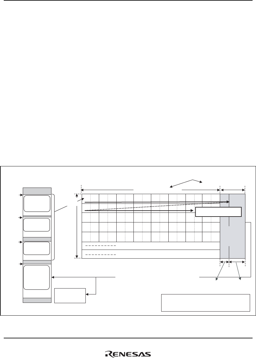
20. Graphics Data Translation Accelerator (GDTA)
Rev.1.00 Jan. 10, 2008 Page 1013 of 1658
REJ09B0261-0100
20.4 GDTA Operation
20.4.1 Explanation of CL Operation
By writing 1 to the CL_EN bit in GACER, registers in the CL register unit can be accessed. After
setting, as initial values, the input frame width/height, input padding size, output padding size,
operating mode (and, in ARGB conversion mode, the palette pointer setting), data written in
succession to CLCF is received, and upon receiving four command parameters (input Y/U/V
pointers, output pointer), processing is begun. In processing, data for one input frame as defined
by the settings (width vs. height) is read, and by setting the CL_MD bit in CLCR, YUYV
conversion or ARGB conversion is performed within the module. Processing is performed in
single frame units, and one frame's worth of converted data is transmitted to the output destination.
The CL can store two commands (in register CLCF) and does not accept the command for the next
frame when two commands are already stored (command FIFO full). A judgment as to whether
processing has ended can be made by using either an interrupt or the CL_END bit in GACISR.
(1) Overview of YUYV Conversion Functions
The following shows an outline of the YUYV conversion specification.
Y0 Y1
Y8 Y9
Y2 Y3
U0 U1
U4 U5
U2 U3
Y4 Y5 Y6 Y7
** ** ** **
** ** ** **
** ** ** **
** ** ** **
Input
Y pointer
Input
U pointer
Input
V pointer
Output
pointer
...
(1) Input data
reading
Frame height
.
.
.
.
.
.
...
V0 V1
V4 V5
V2 V3
Y0 U0 Y1 V0
Y8 U0
Y10 U1
Y9 V0
Y2 U1 Y3 V1
Y4 U2 Y5 V2
Y6 U3 Y7 V3
** ** ** **
** ** ** **
.
.
.
** ** ** **
** ** ** **
.
.
.
...
...
DDR2-SDRAM
Frame width (8 pixels in this figure)
Y0 U0 V0
Y1
Y8 U0 V0Y9
Y16 U4 V4Y17
Y24 U8 V8Y25
Y32 U1 V12Y33
Y2 U1 V1
Y3
Y10 U1 V1Y11
Y18 U5 V5Y19
Y26 U9 V9Y27
Y34 U13 V13Y35
Y4 U2 V2
Y5
Y12 U2 V2Y13
Y20 U6 V6Y21
Y28 U10 V10 Y29
Y36 U14 V14 Y37
Y6 U3 V3
Y7
Y14 U3 V3Y15
Y22 U7 V7Y23
Y30 U11 V11Y31
Y38 U15 V15
Y39
External memory
connected to the
local bus
Display image
In the example of this figure, H'8 is set in CLIWR
and H'30 is set in CLOPR.
(2) Rearrangement (with output padding)
Output padding size (= 48 bytes)
Invalid data
Converted data output order
(3) Output data writing (including output padding data)
For output
(= 16 bytes)
Not for output
(= 32 bytes)
Depending on the specified width and padding size,
there may exist either one or neither of "padding data
for output" and "padding data not for output".
Figure 20.3 YUYV Conversion Functions

20. Graphics Data Translation Accelerator (GDTA)
Rev.1.00 Jan. 10, 2008 Page 1014 of 1658
REJ09B0261-0100
Table 20.7 shows YUYV4:2:2 conversion sequence shown in figure 20.3.
No. in the table corresponds to the number used in figure 20.3.
Table 20.7 YUYV4:2:2 Conversion Sequence
No. Operation Description
(1) Input data
reading
YUV-separated input data stored in DDR2-SDRAM is read into the GDTA.
The input data includes padding data with the specified input Y (UV)
padding size, but the GDTA excludes this padding data when reading the
data. However, if the input frame width is not on a 32-byte boundary,
padding data of the amount for 32-byte boundary adjustment is read into
the GDTA. Transfer of data from the DDR2-SDRAM to the GDTA is in 32
byte units, so that the input data size should be an integral multiple of 32
bytes for one line (frame width + input padding). If there are deviations in
the specified padding sizes for Y and U/V, operation is not guaranteed.
(2) Rearrangement YUV data is rearranged according to the format indicated in the display
image of figure 20.3.
(When converting from YUYV 4:2:0 to YUYV 4:2:2, because the data
quantity for UV is 1/2 that for Y, the UV data in even lines is used for the UV
data in odd lines. For example, the UV data in line 0 is also used in line 1.)
Converted data is output in the converted data output order of the display
image diagram of figure 20.3, regardless of the output destination.
Before the converted data is output, padding data of the size specified by
the CLOPR register is added.
(3) Output data
writing
Because output data is transferred in 32 byte units, one line of output data,
including output padding, should be made an integral multiple of 32 bytes.
(Similarly when the transfer destination is an external device, one line
should be an integral multiple of 32 bytes.)
Padding data other than that used for adjustment for the 32-byte boundary
is not output.
The output data write address for the next line output is calculated by
adding, to the current write address, the size of the padding data that is
specified as the output padding size for each line.
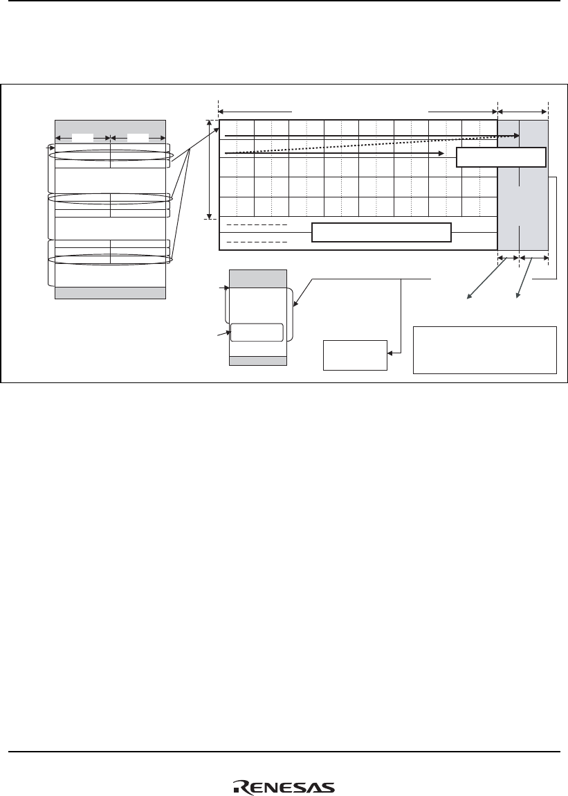
20. Graphics Data Translation Accelerator (GDTA)
Rev.1.00 Jan. 10, 2008 Page 1015 of 1658
REJ09B0261-0100
(2) Overview of ARGB Conversion Functions
The following shows an outline of the ARGB conversion specification.
Frame height
DDR2-SDRAM
AR B
G
AR BG
AR BG
AR BG
AR BG
AR B
G
AR BG
BR BG
BR BG
BR BG
AR B
G
AR B G
AR B G
AR B G
AR B G
A R B
G
A R BG
A R BG
A R BG
A R B
G
External memory
connected to the
local bus
U0: -0.392 (U-128)
AY1: 1.164 (Y-16)
U1: 2.017 (U-128)
V0: 1.596 (V-128) V1: -0.813 (V-128)
U0: -0.392 (U-128)
AY1: 1.164 (Y-16)
U1: 2.017 (U-128)
V0: 1.596 (V-128) V1: -0.813 (V-128)
U0: -0.392 (U-128)
AY1: 1.164 (Y-16)
U1: 2.017 (U-128)
V0: 1.596 (V-128) V1: -0.813 (V-128)
.
.
.
.
16 bits 16 bits
.
.
.
.
.
.
.
.
.
.
.
.
.
.
.
.
.
.
.
.
ARGB
ARGB
ARGB
ARGB
ARGB
ARGB
** ** ** **
** ** ** **
Output pointer
.
.
Output padding size
data inserted
Multiple of 32 bytes of data
Buffer RAM 0
Display image
Frame width (4 pixels in this sample figure)
Invalid data
Converted data output order
Output padding size (= 48 bytes)
(4) ARGB conversion (with output padding)
(3) Color
information
reading
(5) Output data writing
(including output padding data)
For output
(= 16 bytes)
Not for output
(= 32 bytes)
Depending on the specified width and
padding size, there may exist either one or
neither of "padding data for output" and
"padding data not for output".
Data for the
frame width
of 1 line
Pallete
Pointer
256 entries
256 entries
256 entries
Figure 20.4 ARGB Conversion Functions

20. Graphics Data Translation Accelerator (GDTA)
Rev.1.00 Jan. 10, 2008 Page 1016 of 1658
REJ09B0261-0100
Table 20.8 shows ARGB8888 conversion sequence shown in figure 20.4.
No. in the table corresponds to the number used in figure 20.4. (1) and (2) correspond to the
numbers in figure 20.3.
Table 20.8 ARGB8888 Conversion Sequence
No. Operation Description
(1) Input data
reading
YUV-separated input data stored in DDR2-SDRAM is read into the GDTA.
The input data includes padding data with the specified input Y (UV)
padding size, but the GDTA excludes this padding data when reading the
data. However, if the input frame width is not on a 32-byte boundary,
padding data of the amount for 32-byte boundary adjustment is read into the
GDTA. Transfer of data from the DDR2-SDRAM to the GDTA is in 32 byte
units, so that the input data size should be an integral multiple of 32 bytes
for one line (frame width + input padding). If there are deviations in the
specified padding sizes for Y and U/V, operation is not guaranteed.
(2) Rearrangement YUV data is rearranged according to the format indicated in the display
image of figure 20.3.
(When converting from YUV 4:2:0 to YUV 4:2:2, because the data quantity
for UV is 1/2 that for Y, the UV data in even lines is used for the UV data in
odd lines. For example, the UV data in line 0 is also used in line 1.)
(3) Color
information
reading
Data converted in (2) is used as the address of the color conversion table
stored in buffer RAM 0 (CLPLPR setting address + converted data), and
color information is read from buffer RAM 0.
(Converted data: Data converted in (2) is shifted two bits to the left and
added to be the RAM 0 address.)
(Color information is read from the buffer RAM 0 address calculated by
adding the Y value read from DDR2-SDRAM to the buffer RAM 0 palette
pointer value (the address set in CLPLPR). (Same for U and V))

20. Graphics Data Translation Accelerator (GDTA)
Rev.1.00 Jan. 10, 2008 Page 1017 of 1658
REJ09B0261-0100
No. Operation Description
(4) ARGB
conversion
ARGB data is generated from color information read from buffer RAM 0
using the following formula, and the converted data is output in the format
shown in the display image of figure 20.4. ARGB conversion is performed
according to the following conversion logic.
A = The result of computation of clip_0_255((A+16)>> 5) for unsigned 16-bit
data (11 integer bits, 5 decimal bits) read from RAM 0 is output.
R = clip_0_255((Y1 + V0 + 16) >> 5);
G = clip_0_255((Y1 + U0 + V1 + 16) >> 5);
B = clip_0_255((Y1 + U1 + 16) >> 5);
When Y1 = 0, the conversion result is R, G, B = 0.
clip_0_255: 8-bit saturation calculation (0 ≤ x ≤ 255) (the sign is determined
by the uppermost bit (bit 15))
The converted data is output according to the conversion data output order
in the display image of figure 20.4, regardless of the output destination.
Converted data is output by the size 4 x the frame width specified by
CLWR, rounded up to an integral multiple of 32 bytes.
(5) Output data
writing
Because output data is transferred in 32 byte units, one line of output data,
including output padding, should be made an integral multiple of 32 bytes.
Padding data other than that used for adjustment for the 32-byte boundary
is not output.
The output data write address for the next line output is calculated by
adding, to the current write address, the size of the padding data that is
specified as the output padding size for each line.
(3) CL Processing Procedure
Various initial settings are made by the CPU, and processing is started. The processing procedure
is the same for YUYV conversion mode and for ARGB conversion mode, except that in ARGB
conversion mode the data of the color conversion table must be prepared in buffer RAM 0. The
procedure is described below.
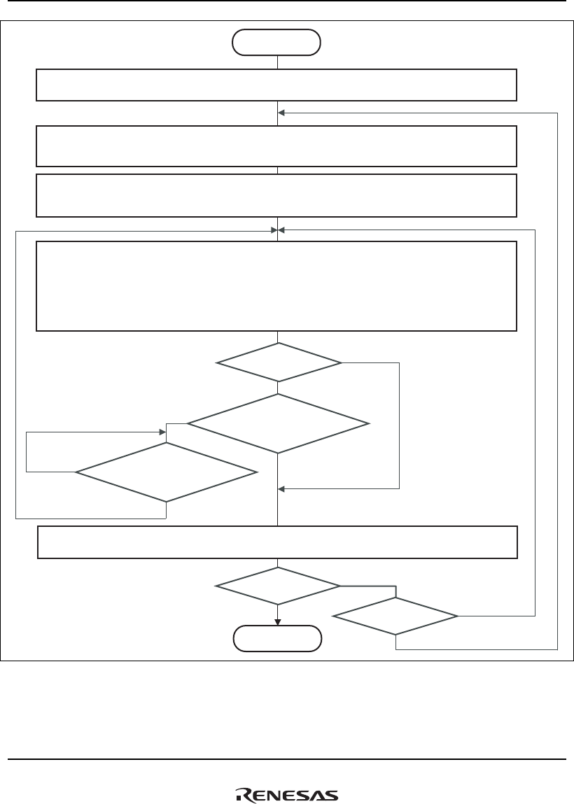
20. Graphics Data Translation Accelerator (GDTA)
Rev.1.00 Jan. 10, 2008 Page 1018 of 1658
REJ09B0261-0100
[Step (1) Clear the CL access mask]
After the CPU sets the key code in GACMR within the bus interface, set GACER to enable access to the CL function block.
[Step (2) Initialize the CL function block]
The CPU sets the frame width/height, input Y/UV padding size, output padding size, and output data/address mode.
In ARGB conversion mode, CLPLPR should also be set.
[Step (5) Wait for processing completion]
Processing completion is judged using an interrupt from the CPU or the CL_END bit in GACISR.
[Step (3) Write the color conversion table to RAM 0]
The CPU writes the color conversion table to RAM 0.
* Step (3) is not necessary in YUYV conversion mode; it is only required in ARGB conversion mode.
[Step (4) Write to the command FIFO]
The CPU writes commands to CLCF. Four command parameters are required
and should be written in succession in the following order:
(1) Data for writing: Input Y pointer
(2) Data for writing: Input U pointer
(3) Data for writing: Input V pointer
(4) Data for writing: Output pointer
Continuous processing?
Next processing?
End
Start
Is continuous processing
timed by interrupt or setting of the
CL_END bit in GACISR?
Is the CL command FIFO full?
(Check the CK_CFF bit in CLSR.)
Change settings
for CL processing?
No
No
No
No No
Yes
Yes
Yes
Yes
Yes
Figure 20.5 CL Processing Procedure

20. Graphics Data Translation Accelerator (GDTA)
Rev.1.00 Jan. 10, 2008 Page 1019 of 1658
REJ09B0261-0100
20.4.2 Explanation of MC Operation
By writing 1 to the MC_EN bit in GACER, registers in the MC register unit can be accessed.
After setting, as initial values, the input frame width/height, input YUV padding size, output frame
YUV pointer, past frame YUV pointer and future frame YUV pointer, data written in succession
to MCCF is received, and upon receiving a maximum of eight command parameters (estimating
mode, vector, buffer RAM 1 address), processing is begun. In processing, data is read in
macroblock units (Y: 16 pixels × 16 lines, U/V: 8 pixels × 8 lines), and estimated image
generation is performed within the module. The generated image by the amount of a macroblock
is output to the output destination.
The MC can store four commands (in register MCCF) and does not accept the command for the
next frame when four commands are already stored (command FIFO full). A judgment as to
whether processing has ended can be made by using either an interrupt or the MC_END bit in
GACISR.
Figure 20.6 illustrates the processing of one Y macroblock in "forward macroblock processing".
(After three rounds of processing for Y, U, and V have been done, a processing-end interrupt is
generated by writing an end command.) On the other hand, in "reverse macroblock processing" the
address for reading data from DDR2, shown in figure 20.6, is changed to the future frame pointer,
and other processing is the same. Hence in "bidirectional macroblock processing", (half-pixel-
corrected past data + half-pixel-corrected future data + 1)/2 is taken to be the correction processing
result, and calculation is performed with the IDCT data.
Finally, in "intra macroblock processing" signed IDCT data (the sign of which is discriminated
using the uppermost bit (bit 15)) is converted into unsigned 8-bit data and written to the output
position.
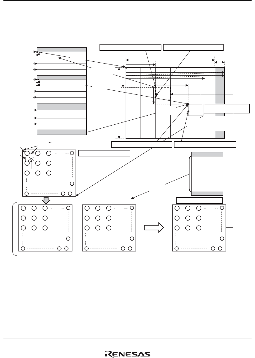
20. Graphics Data Translation Accelerator (GDTA)
Rev.1.00 Jan. 10, 2008 Page 1020 of 1658
REJ09B0261-0100
(1) Estimated Image Generation Function
The following shows an outline of the estimated image generation function.
Output frame
Y pointer (current)
Output frame
U pointer (current)
Output frame
V pointer (current)
Past frame
Y pointer
Past frame
U pointer
Past frame
V pointer
Future frame
Y pointer
Future frame
U pointer
Future frame
V pointer
(9) Estimated
image writing
(5) Data
reading
Image data for one frame
Frame width
Y padding
U (current)
V (current)
U (past)
V (past)
Y (future)
U (future)
V (future)
Y (past)
Y (current)
Base point
Base point
Output
(current)
Output
target position
Target position (mbcol, mbrow)
Comparison point
(+Recon_right, down)
(6) Half-pixel correction processing
Recon_down
(negative value indicates reverse direction)
Invalid data
Y: 16 × 16 dot
U: 8 × 8 dot
V: 8 × 8 dot
Input
image
(half-pixel)
Recon_right (negative value indicates reverse direction)
Y: 17 × 17 dot
U: 9 × 9 dot
V: 9 × 9 dot
For half-pixel processing,
get data for a block with one
extra dot according to motion
vector values
Hardware performs processing
as is even when in padding part
Y0 (128 bytes)
Y1 (128 bytes)
Y2 (128 bytes)
Y3 (128 bytes)
U (128 bytes)
V (128 bytes)
Buffer RAM 1
(8) Estimated-image generation
(7) IDCT data
reading
IDCT data
Y: 16 × 16 dot
U: 8 × 8 dot
V: 8 × 8 dot
Y: 16 × 16 dot
U: 8 × 8 dot
V: 8 × 8 dot
Y: 17 × 17 dot
U: 9 × 9 dot
V: 9 × 9 dot
Y: 16 × 16 dot
U: 8 × 8 dot
V: 8 × 8 dot
Correction processing result (Y: 16 × 16, U/V: 8 × 8)
Data after half-pixel
correction
IDCT data
Data to be written back to the current target position
(result of forward macroblock processing)
× 16
× 16
× 16
× 16
× 16
× 16
× 17
× 17
Input data for one macroblock
Correction
case 3
Correction case 4
Correction
case 1
Correction
case 2
Each frame pointer should point to an address on a 16-byte boundary
for Y and 8-byte boundary for U and V.
8-bit saturation
calculation
(0 ≤ x ≤ 255)
(1) Calculation of output position (first row) (2) Calculation of output position (nth row)
(3) Calculation of input position (first row) (4) Calculation of input position (nth row)
AB
ED
A' B'
D'C'
ab
d
c
A'' B'
D'C'
mbcol
mbrow
Frame height
(mbcol, mbrow)
DDR2-SDRAM
Figure 20.6 Outline of Estimated Image Generation Function

20. Graphics Data Translation Accelerator (GDTA)
Rev.1.00 Jan. 10, 2008 Page 1021 of 1658
REJ09B0261-0100
Table 20.9 shows estimated image generation sequence shown in figure 20.6.
No. in the table corresponds to the number used in figure 20.6.
Table 20.9 Estimated Image Generation Sequence
No. Operation Description
(1) Calculation of
output position
(first row)
The following formulae are used to compute output position (first row) (DDR2-
SDRAM output address).
First row output address formulae
• Y output target address
Calculation formula: Output frame Y point value (base point) + [mbrow ×
16 × (width + Y padding)] + [mbcol × 16]
Output frame Y pointer value (base point): MCOYPR setting address
mbrow: Calculated from MCCF setting
mbcol: Calculated from MCCF setting
width: Calculated from MCWR setting
Y padding: Calculated from MCYPR setting
Subsequently, data for 16 dots (= 16 bytes) is processed in succession
• U/V output target address
Calculation formula: Output frame U point value (base point) + [mbrow × 8
× (width/2 + U padding)] + [mbcol × 8]
Output frame U pointer value (base point): MCOUPR setting address
mbrow: Calculated from MCCF setting
mbcol: Calculated from MCCF setting
width: Calculated from MCWR setting
U padding: Calculated from MCUVPR setting
Subsequently, data for 8 dots (= 8 bytes) is processed in succession
V pointer address is calculated using a formula similar to that for the U pointer
address.

20. Graphics Data Translation Accelerator (GDTA)
Rev.1.00 Jan. 10, 2008 Page 1022 of 1658
REJ09B0261-0100
No. Operation Description
(2) Calculation of
output position
(nth row and
below)
The following formulae are used to compute output positions (nth row and
below) (DDR2-SDRAM output address).
Output address formulae for nth row and below
• Y output target address
Calculation formula: Output frame Y point value (base point) + [(mbrow ×
16 + n - 1) × (width + Y padding)] + [mbcol × 16]
Output frame Y pointer value (base point): MCOYPR setting address
mbrow: Calculated from MCCF setting
mbcol: Calculated from MCCF setting
width: Calculated from MCWR setting
Y padding: Calculated from MCYPR setting
Subsequently, data for 16 dots (= 16 bytes) is processed in succession
• U/V output target address
Calculation formula: Output frame U point value (base point) + [(mbrow ×
8 + n - 1) × (width/2 + U padding)] + [mbcol × 8]
Output frame U pointer value (base point): MCOUPR setting address
mbrow: Calculated from MCCF setting
mbcol: Calculated from MCCF setting
width: Calculated from MCWR setting
U padding: Calculated from MCUVPR setting
Subsequently, data for 8 dots (= 8 bytes) is processed in succession
V pointer address is calculated using a formula similar to that for the U pointer
address.

20. Graphics Data Translation Accelerator (GDTA)
Rev.1.00 Jan. 10, 2008 Page 1023 of 1658
REJ09B0261-0100
No. Operation Description
(3) Calculation of
input position
(first row)
The following formulae are used to compute input position (first row) (DDR2-
SDRAM input address).
First row input address formulae
• Y input comparison address
Calculation formula: Past frame Y point value (base point) + [(mbrow × 16
+ (Recon_down>>1)) × (width + Y padding)] + [mbcol × 16 +
(Recon_right>>1)]
Past frame Y pointer value (base point): MCPYPR setting address
mbrow: Calculated from MCCF setting
mbcol: Calculated from MCCF setting
Recon_down: Calculated from MCCF setting
Recon_right: Calculated from MCCF setting
width: Calculated from MCWR setting
Y padding: Calculated from MCYPR setting
Depending on the motion vector value, 16-dot data (16 bytes) or 17-dot data
(17 bytes) is processed in succession.
Future frame Y pointer address is calculated using a formula similar to that for
the past frame.
* Calculation result for Recon_down>>1 is shown below:
Recon_
down
-6 -5 -4 -3 -2 -1 0 1 2 3 4 5 6
Recon_
down>>1
-3 -3 -2 -2 -1 -1 0 0 1 1 2 2 3
Calculation result for Recon_right>>1 is the same.

20. Graphics Data Translation Accelerator (GDTA)
Rev.1.00 Jan. 10, 2008 Page 1024 of 1658
REJ09B0261-0100
No. Operation Description
(3) Calculation of
input position
(first row)
• U/V input comparison address
Calculation formula: Past frame U point value (base point) + [(mbrow × 8 +
(Recon_down/2>>1)) × (width/2 + U padding)] + [mbcol × 8 +
(Recon_right/2>>1)]
Past frame U pointer value (base point): MCPUPR setting address
mbrow: Calculated from MCCF setting
mbcol: Calculated from MCCF setting
Recon_down: Calculated from MCCF setting
Recon_right: Calculated from MCCF setting
width: Calculated from MCWR setting
U padding: Calculated from MCUVPR setting
Depending on the motion vector value, 8-dot data (8 bytes) or 9-dot data (9
bytes) is processed in succession.
Future frame U pointer address is calculated using a formula similar to that for
the past frame.
V pointer address is calculated using a formula similar to that for the U pointer
address.
* Calculation result for Recon_down/2>>1 is shown below:
Recon_
down
-6 -5 -4 -3 -2 -1 0 1 2 3 4 5 6
Recon_
down/2>>1
-2 -1 -1 -1 -1 0 0 0 0 0 1 1 1
Calculation result for Recon_right/2>>1 is the same.

20. Graphics Data Translation Accelerator (GDTA)
Rev.1.00 Jan. 10, 2008 Page 1025 of 1658
REJ09B0261-0100
No. Operation Description
(4) Calculation of
input position
(nth row and
below)
The following formulae are used to compute input positions (nth row and
below) (DDR2-SDRAM input address).
Input address formulae for nth row and below
• Y input comparison address
Calculation formula: Past frame Y point value (base point) + [(mbrow × 16
+ (Recon_down>>1) + n - 1) × (width + Y padding)] + [mbcol × 16 +
(Recon_right>>1)]
Past frame Y pointer value (base point): MCPYPR setting address
mbrow: Calculated from MCCF setting
mbcol: Calculated from MCCF setting
Recon_down: Calculated from MCCF setting
Recon_right: Calculated from MCCF setting
width: Calculated from MCWR setting
Y padding: Calculated from MCYPR setting
Depending on the motion vector value, 16-dot data (16 bytes) or 17-dot data
(17 bytes) is processed in succession.
Future frame Y pointer address is calculated using a formula similar to that for
the past frame.
• U/V input comparison address
Calculation formula: Past frame U point value (base point) + [(mbrow × 8 +
(Recon_down/2>>1) + n - 1) × (width/2 + U padding)] + [mbcol × 8 +
((Recon_right/2)>>1)]
Past frame U pointer value (base point): MCPUPR setting address
mbrow: Calculated from MCCF setting
mbcol: Calculated from MCCF setting
Recon_down: Calculated from MCCF setting
Recon_right: Calculated from MCCF setting
width: Calculated from MCWR setting
U padding: Calculated from MCUVPR setting
Depending on the motion vector value, 8-dot data (8 bytes) or 9-dot data (9
bytes) is processed in succession.
Future frame U pointer address is calculated using a formula similar to that for
the past frame.
V pointer address is calculated using a formula similar to that for the U pointer
address.
(5) Data reading Input data stored in DDR2-SDRAM is read into the GDTA at the address
computed in (3) and (4).
20. Graphics Data Translation Accelerator (GDTA)
Rev.1.00 Jan. 10, 2008 Page 1026 of 1658
REJ09B0261-0100
No. Operation Description
(6) Half-pixel
correction
processing
Half-pixel correction processing is performed for the data read in (5).
(For the Y pointer: 16 to the right and 16 downward in 4 pixel units, for a total
of 256 processed)
* The Recon_down value is used to perform half-pixel correction even/odd
decisions. Decision results are as follows.
(The Recon_right value is similarly used to perform half-pixel correction
even/odd decisions.)
Recon_down -6 -5 -4 -3 -2 -1 0 1 2 3 4 5 6
Y even/odd even odd even odd even odd even odd even odd even odd even
U/V
even/odd
odd even even odd odd even even even odd odd even even odd
Formulae for each correction case at "Input data for one macroblock" in figure
20.6 are as follows.
Correction case 1: right = even, down = even
-> (A + A + 1)/2 = A (digits below the decimal point are discarded (no
change))
Correction case 2: right = even, down = odd
-> (A + C + 1)/2 = A' (digits below the decimal point are discarded)
Correction case 3: right = odd, down = even
-> (A + B + 1)/2 = A' (digits below the decimal point are discarded)
Correction case 4: right = odd, down = odd
-> (A + D + B + C + 2)/4 = A' (digits below the decimal point are discarded)
In bidirectional macroblock processing, the result of computation of the
following formula using past data after half-pixel correction and future data
after half-pixel correction is taken to be the half-pixel correction result, and
computation processing with IDCT data is performed.
(past data after half-pixel correction + future data after half-pixel correction
+1)/2 = half-pixel correction result
There are cases in which, due to the settings, input macroblock data is not
within the padding area and the data exceeds the screen height (invalid
image data), but the hardware performs processing without modification.

20. Graphics Data Translation Accelerator (GDTA)
Rev.1.00 Jan. 10, 2008 Page 1027 of 1658
REJ09B0261-0100
No. Operation Description
(7) IDCT data
reading
IDCT data stored in buffer RAM 1 is read.
(Only blocks specified by a CBP setting of 1 are read from buffer RAM 1.)
The IDCT data should be stored in buffer RAM 1 as 16-bit signed data.
(The sign is discriminated using the uppermost bit (bit 15).)
Regardless of the CBP value, the IDCT data should be stored in successive
addresses in the order Y0 (128 bytes), Y1 (128 bytes), Y2 (128 bytes), Y3
(128 bytes), U (128 bytes), V (128 bytes).
When there is a CBP=0 block, the address space should not be packed, but
data should be stored in successive addresses in the Y0, Y1, Y2, Y3, U, V
data format.
The CBP value indicates whether a sign is required compared with the
comparison image for the six blocks (four luminance blocks and two
chrominance blocks). The above Y0, Y1, Y2, Y3, U, V are CBP values of
block positions in the following format.
CBP Blocks with YUV4:2:0
Y0 Y1 U
Luminance Y Y2 Y3
Chrominance
U/V V
(Data for a CBP=0 block: data invalid)
9-bit saturation computation is performed for IDCT data read from RAM 1 (-
256 ≤ x ≤ 255).
(The sign is discriminated using the uppermost bit (bit 15).)
IDCT data reading is performed in parallel with the operation of (5) and (6).
(8) Estimated
image data
generation
Estimated image data is generated using the following formula from the half-
pixel processing data generated in (6) and the IDCT data (9-bit data after
saturation computation) read in (7).
Formula: (data of (6) + data of (7)) -> (saturation computation) (0 ≤ x ≤ 255)
(9) Estimated
image data
writing
Estimated image data is written to DDR2-SDRAM at the address computed in
(1) and (2).
(2) MC Processing Procedure
The CPU performs required initialization and starts the processing. IDCT data must be prepared in
the buffer RAM 1. The procedure is shown below.
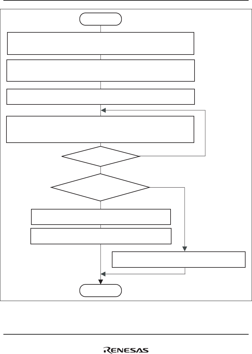
20. Graphics Data Translation Accelerator (GDTA)
Rev.1.00 Jan. 10, 2008 Page 1028 of 1658
REJ09B0261-0100
Start
End
Is an interrupt used to recognize
processing completion?
Continuous processing?
[Step (1) Clear the MC access mask]
After the CPU sets the key code in GACMR within the bus interface,
set GACER to enable access to the MC function block.
[Step (2) Initialize the MC function block]
The CPU sets the frame width/height, input Y/UV padding size, output frame Y/U/V pointers,
past frame Y/U/V pointers, and future frame Y/U/V pointers.
[Step (3) Write IDCT data to RAM 1]
The CPU writes IDCT data to RAM 1.
[Step (4) Write commands to FIFO]
The CPU writes commands to MCCF. Eight command parameters are required,
and are written in sequence.
For details of settings, refer to section 20.3.21, MC Command FIFO (MCCF).
[Step (5) Write the end command to command FIFO]
The CPU writes the end command to MCCF.
[Step (7) Check the register to confirm processing completion]
Processing completion is judged using the MC_END bit in GACISR.
[Step (6) Wait for an interrupt signaling processing completion]
Processing completion is judged using an interrupt from the CPU.
No
No
Yes
Yes
Figure 20.7 MC Processing Procedure

20. Graphics Data Translation Accelerator (GDTA)
Rev.1.00 Jan. 10, 2008 Page 1029 of 1658
REJ09B0261-0100
20.5 Interrupt Processing
In the GDTA, there are four types of interrupt sources. There are three interrupt flags for CL
processing end, MC processing end, and CL/MC errors, used to identify interrupt sources. The
interrupt enable bit allows generation of interrupt requests.
CL errors and MC errors use a common GAERI interrupt.
Table 20.10 GDTA Interrupt Request
Interrupt Source Interrupt Flag Enable Bit Description
CL_END interrupt CL_END CL_ENEN CL processing ended
MC_END interrupt MC_END MC_ENEN MC processing ended
CL_ERR interrupt CL_ERR or MC_ERR CL_EREN CL error occurred
MC_ERR interrupt MC_EREN MC error occurred
20.6 Data Alignment
The GDTA performs data alignment conversion of input data, output data, and RAM 0/1 data
using an endian signal (pin MD8) or using GDTA internal registers.
Table 20.11 shows the correspondence between data alignment conversion patterns and the
settings of DRCL_CTL, DWCL_CTL, DRMC_CTL, DWMC_CTL, DCP_CTL, and DID_CTL.
Table 20.11 GDTA Data Alignment Conversion
DTAM DTSA DTUA Little (MD8) Data Alignment Conversion Pattern Remarks
0 H'00 H'00 0 CP3 (2)
0 H'00 H'00 1 CP3 (1)
1 H'00 H'00 * CP3 (2)
1 H'01 H'01 * CP1 (1)
1 H'01 H'10 * CP2 (1)
1 H'01 H'11 * CP3 (1)
1 H'10 H'01 * CP1 (2)
1 H'10 H'10 * CP2 (2)
1 H'11 H'01 * CP1 (3)
Note: * For the data alignment pattern numbers, refer to figure 20.8.
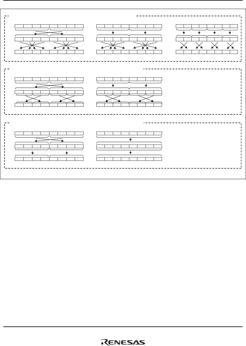
20. Graphics Data Translation Accelerator (GDTA)
Rev.1.00 Jan. 10, 2008 Page 1030 of 1658
REJ09B0261-0100
D0 D1 D2 D3 D4 D5 D6 D7
D4 D5 D6 D7 D0 D1 D2 D3
D7 D6 D5 D4 D3 D2 D1 D0
D0 D1 D2 D3 D4 D5 D6 D7
D0 D1 D2 D3 D4 D5 D6 D7
D3 D2 D1 D0 D7 D6 D5 D4
D0 D1 D2 D3 D4 D5 D6 D7
D0 D1 D2 D3 D4 D5 D6 D7
D1 D0 D3 D2 D5 D4 D7 D6
D0 D1 D2 D3 D4 D5 D6 D7
D0 D1 D2 D3 D4 D5 D6 D7
D2 D3 D0 D1 D6 D7 D4 D5
D0 D1 D2 D3 D4 D5 D6 D7
D0 D1 D2 D3 D4 D5 D6 D7
D0 D1 D2 D3 D4 D5 D6 D7
D0 D1 D2 D3 D4 D5 D6 D7
D4 D5 D6 D7 D0 D1 D1 D3
D6 D7 D4 D5 D2 D3 D0 D1
D0 D1 D2 D3 D4 D5 D6 D7
D4 D5 D6 D7 D0 D1 D2 D3
D4 D5 D6 D7 D0 D1 D2 D3
63 56 55 48 47 40 39 32 31 24 23 16 15 8 7 0
63 56 55 48 47 40 39 32 31 24 23 16 15 8 7 0
63 56 55 48 47 40 39 32 31 24 23 16 15 8 7 0 63 56 55 48 47 40 39 32 31 24 23 16 15 8 7 0
63 56 55 48 47 40 39 32 31 24 23 16 15 8 7 0
63 56 55 48 47 40 39 32 31 24 23 16 15 8 7 0 63 56 55 48 47 40 39 32 31 24 23 16 15 8 7 0
Data alignment unit: 1 byte Conversion pattern 1 (CP1)
Data alignment unit: 2 bytes Conversion pattern 2 (CP2)
Data alignment unit: 3 bytes Conversion pattern 3 (CP3)
2.1. 3.
1. 2.
1. 2.
* D0 to D7 above indicate byte data on the SHwy.
Figure 20.8 Data Alignment Conversion Pattern

20. Graphics Data Translation Accelerator (GDTA)
Rev.1.00 Jan. 10, 2008 Page 1031 of 1658
REJ09B0261-0100
20.7 Usage Notes
When using the GDTA, note the following:
20.7.1 Regarding Module Stoppage
During GDTA operation, the CPG register settings must not be done to stop a module (other
modules as well as the GDTA). If a module is stopped during GDTA operation, the GDTA
processing is stopped and processing contents set in CL/MC command FIFO are cleared.
When stopping the module, settings should be changed to stop the module only after confirming
that the CLSR.EXE bit (bit 3) in CLSR is 0 and the MC_CFA bits (bits 10 to 8) in MCSR are 000.
In order to resume the processing, the procedure described in section 20.4.1 (3), CL Processing
Procedure or section 20.4.2 (2), MC Processing Procedure should be used after releasing the
module stop. (After a module is stopped, the processing that was in progress and processing
contents set in the CL/MC command FIFO should be performed again.)
20.7.2 Regarding Deep Sleep Modes
During GDTA operation, deep sleep mode must not be entered. If a transition is made to deep
sleep mode during GDTA operation, the GDTA processing is stopped and processing contents set
in CL/MC command FIFO are cleared.
When entering deep sleep mode, a transition should be made only after confirming that the
CLSR.EXE bit (bit 3) in CLSR is 0, and also after confirming that the MC_CFA bits (bits 10 to 8)
in MCSR are 000.
In order to resume the processing, the procedure described in section 20.4.1 (3), CL Processing
Procedure or section 20.4.2 (2), MC Processing Procedure should be used after releasing the deep
sleep mode. (After deep sleep mode is entered, the processing that was in progress and processing
contents set in the CL/MC command FIFO should be performed again.)

20. Graphics Data Translation Accelerator (GDTA)
Rev.1.00 Jan. 10, 2008 Page 1032 of 1658
REJ09B0261-0100
20.7.3 Regarding Frequency Changes
During GDTA operation, the CPG register setting must not be used to change frequency. If
frequency is changed during GDTA operation, the GDTA processing is stopped and processing
contents set in CL/MC command FIFO are cleared.
When changing the frequency, the frequency should be changed only after confirming that the
CLSR.EXE bit (bit 3) in CLSR is 0 and the MC_CFA bits (bits 10 to 8) in MCSR are 000.
When resuming the processing, the procedure described in section 20.4.1 (3), CL Processing
Procedure or section 20.4.2 (2), MC Processing Procedure should be used after changing the
frequency. (After a frequency is changed, the processing that was in progress and processing
contents set in the CL/MC command FIFO should be performed again.)

21. Serial Communication Interface with FIFO (SCIF)
Rev.1.00 Jan. 10, 2008 Page 1033 of 1658
REJ09B0261-0100
Section 21 Serial Communication Interface with FIFO
(SCIF)
This LSI is equipped with a 6-channel serial communication interface with built-in FIFO buffers
(Serial Communication Interface with FIFO: SCIF). The SCIF can perform both asynchronous and
clocked synchronous serial communications.
64-stage FIFO buffers are provided for transmission and reception, enabling fast, efficient, and
continuous communication.
Channel 0 has modem control functions (RTS and CTS).
21.1 Features
The SCIF has the following features.
• Asynchronous serial communication mode
Serial data communication is executed using an asynchronous system in which
synchronization is achieved character by character. Serial data communication can be carried
out with standard asynchronous communication chips such as a Universal Asynchronous
Receiver/Transmitter (UART) or Asynchronous Communication Interface Adapter (ACIA).
There is a choice of 8 serial data transfer formats.
⎯ Data length: 7 or 8 bits
⎯ Stop bit length: 1 or 2 bits
⎯ Parity: Even/odd/none
⎯ Receive error detection: Parity, framing, and overrun errors
⎯ Break detection: A break is detected when a framing error lasts for more than 1 frame
length at Space 0 (low level). When a framing error occurs, a break can also be detected by
reading the SCIF0_RXD to SCIF5_RXD pin levels directly from the serial port register
(SCSPTR).
• Clocked synchronous serial communication mode
Serial data communication is synchronized with a clock. Serial data communication can be
carried out with other LSIs that have a synchronous communication function.
There is a single serial data communication format.
Data length: 8 bits
Receive error detection: Overrun errors

21. Serial Communication Interface with FIFO (SCIF)
Rev.1.00 Jan. 10, 2008 Page 1034 of 1658
REJ09B0261-0100
• Full-duplex communication capability
The transmitter and receiver are independent units, enabling transmission and reception to be
performed simultaneously.
The transmitter and receiver both have a 64-stage FIFO buffer structure, enabling continuous
transmission and reception of serial data.
• LSB first for data transmission and reception
• On-chip baud rate generator allows any bit rate to be selected.
• Choice of clock source: internal clock from baud rate generator or external clock from
SCIF0_SCK to SCIF5_SCK pins
• Four interrupt sources
There are four interrupt sources – transmit-FIFO-data-empty, break, receive-FIFO-data-full,
and receive error – that can issue requests independently.
• The DMA controller (DMAC) can be activated to execute a data transfer by issuing a DMA
transfer request in the event of a transmit-FIFO-data-empty or receive-FIFO-data-full interrupt.
• When not in use, the SCIF can be stopped by halting its clock supply to reduce power
consumption.
• In asynchronous mode, modem control functions (SCIF0_RTS and SCIF0_CTS) are
provided.(only in channel 0)
• The amount of data in the transmit/receive FIFO registers, and the number of receive errors in
the receive data in the receive FIFO register, can be ascertained.
• In asynchronous mode, a timeout error (DR) can be detected during reception.
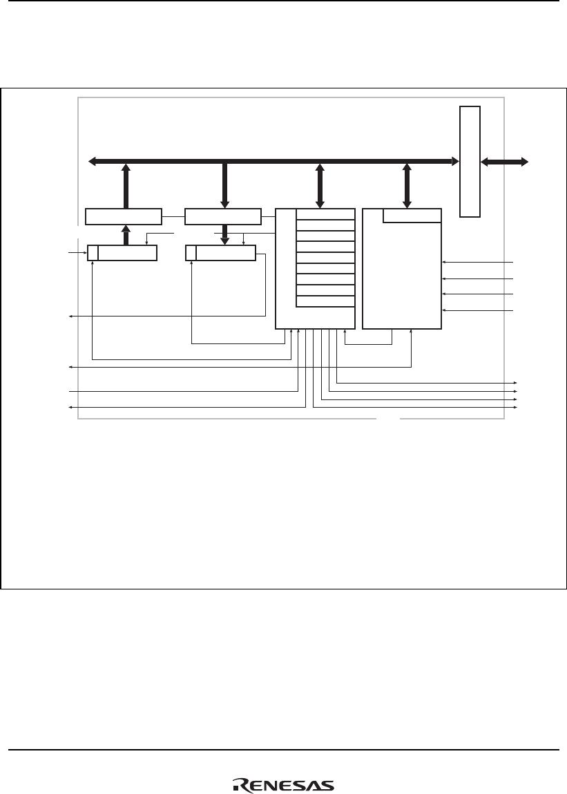
21. Serial Communication Interface with FIFO (SCIF)
Rev.1.00 Jan. 10, 2008 Page 1035 of 1658
REJ09B0261-0100
Figure 21.1 shows a block diagram of the SCIF. Figures 21.2 to 21.6 show block diagrams of the
I/O ports in the SCIF. There are six channels in this LSI. In figures 21.2 to 21.6, the channel
number is omitted.
SCFRDRn (128 stages)
SCRSRn
SCIFn_RXD
SCIFn_TXD
SCIFn_SCK
SCIF0_CTS
SCIF0_RTS
SCFTDRn (128 stages)
SCTSRn
SCTFDRn
SCRFDRn
SCFCRn
SCFSRn
SCSCRn
SCSPTRn
SCRERn
SCLSRn
SCSMRn SCBRRn
Pck
Pck/4
Pck/16
Pck/64
SCIF
Parity generation
Parity check
Module data bus
Transmission/
reception control
Clock
Baud rate generator
Peripheral bus
External clock
Bus interface
(64 stages) (64 stages)
Legend:
SCRSRn: Receive shift register
SCFRDRn: Receive FIFO data register
SCTSRn: Transmit shift register
SCFTDRn: Transmit FIFO data register
SCSMRn: Serial mode register
SCSCRn: Serial control register
SCFSRn: Serial status register
SCBRRn: Bit rate register
SCSPTRn: Serial port register
SCFCRn: FIFO control register
SCTFDRn: Transmit FIFO data count register
SCRFDRn: Receive FIFO data count register
SCLSRn: Line status register
SCRERn: Serial error register
Note: n = 0 to 5
Channels 1 to 5 do not have SCIF1_CTS to SCIF5_CTS and SCIF1_RTS to SCIF5_RTS.
TXIn
RXIn
ERIn
BRIn
Figure 21.1 Block Diagram of SCIF
Figures 21.2 to 21.6 show block diagrams of the I/O ports in SCIF.
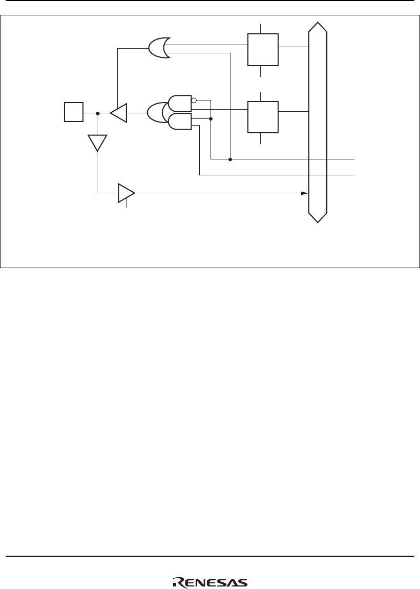
21. Serial Communication Interface with FIFO (SCIF)
Rev.1.00 Jan. 10, 2008 Page 1036 of 1658
REJ09B0261-0100
SPTRW
D7
D6
R
QD
RTSIO
C
SPTRR
SPTRW
R
QD
RTSDT
C
SCIF0_RTS
Reset
Reset
Peripheral bus
Modem control
enable signal*
SCIF0_RTS signal
Legend:
SPTRW: Write to SCSPTR
SPTRR: Read from SCSPTR
Note:
*
SCSPTR The
SCIF0_RTS pin function is designated as modem control by the MCE bit in SCFCR.
Figure 21.2 SCIF0_RTS Pin
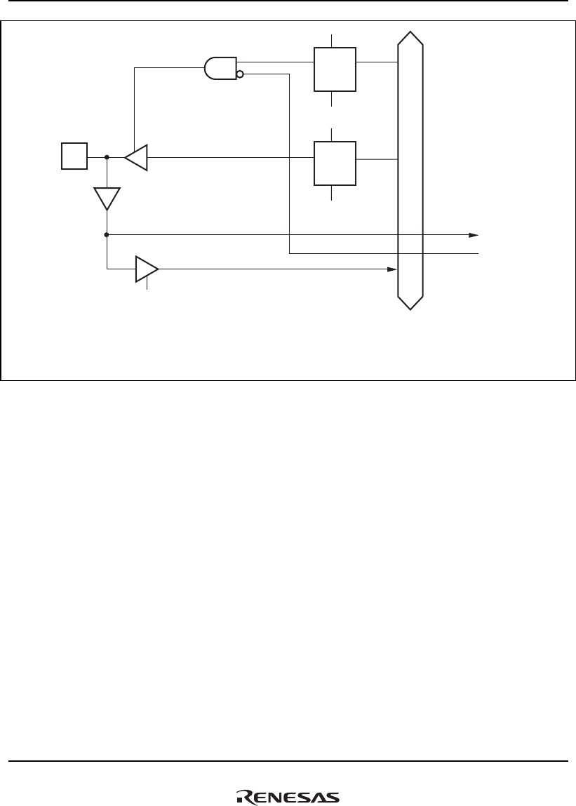
21. Serial Communication Interface with FIFO (SCIF)
Rev.1.00 Jan. 10, 2008 Page 1037 of 1658
REJ09B0261-0100
SPTRW
D5
D4
R
QD
CTSIO
C
SPTRR
SPTRW
R
QD
CTSDT
C
SCIF0_CTS
Legend:
SPTRW: Write to SCSPTR
SPTRR: Read from SCSPTR
Note:
*
The SCIF0_CTS pin function is designated as modem control by the MCE bit in SCFCR.
Modem control enable signal*
SCIF0_CTS signal
Reset
Reset
Peripheral bus
Figure 21.3 SCIF0_CTS Pin
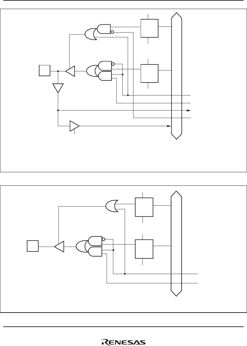
21. Serial Communication Interface with FIFO (SCIF)
Rev.1.00 Jan. 10, 2008 Page 1038 of 1658
REJ09B0261-0100
SPTRW
D3
D2
R
QD
SCKIO
C
SPTRR
SPTRW
R
QD
SCKDT
C
Clock output enable signal*
Serial clock output signal*
Serial clock input signal*
Serial input enable signal*
Peripheral bus
Reset
Reset
Legend:
SPTRW: Write to SCSPTR
SPTRR: Read from SCSPTR
Note: * The SCIFn_SCK pin function is designated as internal clock output or external clock input
by the C/A bit in SCSMR and the CKE1 and CKE0 bits in SCSCR.
SCIFn_SCK
Figure 21.4 SCIFn_SCK Pin (n = 0 to 5)
SPTRW
D1
D0
R
QD
SPB2IO
C
SPTRW
R
QD
SPB2DT
C
Legend:
SPTRW: Write to SCSPTR
SCIFn_TXD
Transmit enable signal
Serial transmit data
Peripheral bus
Reset
Reset
Figure 21.5 SCIFn_TXD Pin (n = 0 to 5)
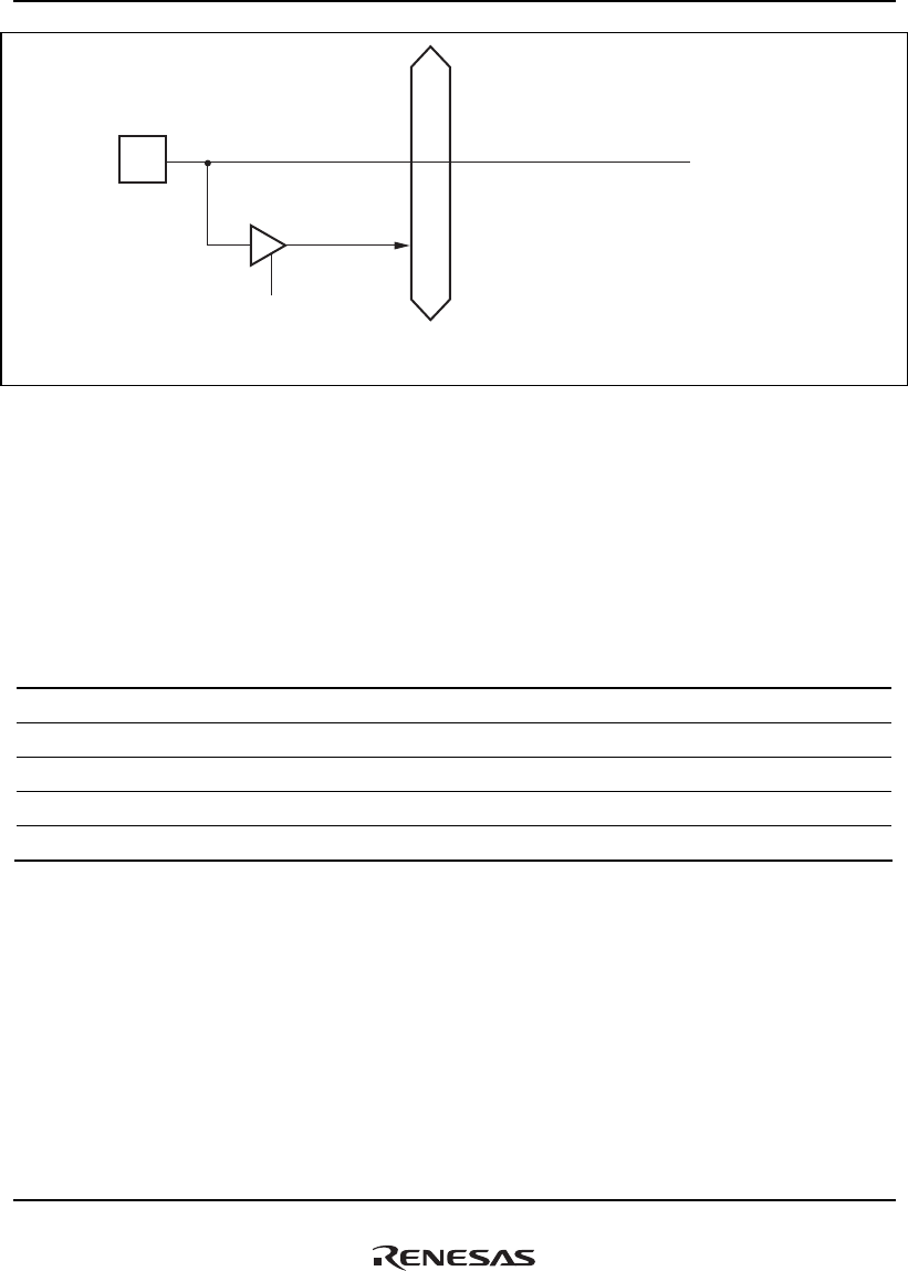
21. Serial Communication Interface with FIFO (SCIF)
Rev.1.00 Jan. 10, 2008 Page 1039 of 1658
REJ09B0261-0100
SPTRR
Legend:
SPTRR: Read from SCSPTR
SCIFn_RXD
Peripheral bus
Serial receive data
Figure 21.6 SCIFn_RXD Pin (n = 0 to 5)
21.2 Input/Output Pins
Table 21.1 shows the SCIF pin configuration. Since the pin functions are the same in each
channel, the channel number is omitted in the description below. The modem control pins are
available only in channel 0.
Table 21.1 Pin Configuration
Pin Name Abbreviation I/O Function
Serial clock pin SCIF0_SCK to SCIF5_SCK I/O Clock input/output
Receive data pin SCIF0_RXD to SCIF5_RXD Input Receive data input
Transmit data pin SCIF0_TXD to SCIF5_TXD Output Transmit data output
Modem control pin SCIF0_CTS I/O Transmission enabled
Modem control pin SCIF0_RTS I/O Transmission request
Note: These pins function as serial pins by performing SCIF operation settings with the C/A bit in
SCSMR, the TE, RE, CKE1, and CKE0 bits in SCSCR, and the MCE bit in SCFCR. Break
state transmission and detection can be set by SCSPTR of the SCIF.

21. Serial Communication Interface with FIFO (SCIF)
Rev.1.00 Jan. 10, 2008 Page 1040 of 1658
REJ09B0261-0100
21.3 Register Descriptions
The SCIF has the following registers. Since the register functions are the same in each channel,
the channel number is omitted in the description below.
Table 21.2 Register Configuration (1)
Ch. Register Name Abbrev. R/W P4 Address Area 7 Address Size
Sync
Clock
0 Serial mode register 0 SCSMR0 R/W H'FFEA 0000 H'1FEA 0000 16 Pck
Bit rate register 0 SCBRR0 R/W H'FFEA 0004 H'1FEA 0004 8 Pck
Serial control register 0 SCSCR0 R/W H'FFEA 0008 H'1FEA 0008 16 Pck
Transmit FIFO data register 0 SCFTDR0 W H'FFEA 000C H'1FEA 000C 8 Pck
Serial status register 0 SCFSR0 R/W*1 H'FFEA 0010 H'1FEA 0010 16 Pck
Receive FIFO data register 0 SCFRDR0 R H'FFEA 0014 H'1FEA 0014 8 Pck
FIFO control register 0 SCFCR0 R/W H'FFEA 0018 H'1FEA 0018 16 Pck
Transmit FIFO data count register 0 SCTFDR0 R H'FFEA 001C H'1FEA 001C 16 Pck
Receive FIFO data count register 0 SCRFDR0 R H'FFEA 0020 H'1FEA 0020 16 Pck
Serial port register 0 SCSPTR0 R/W H'FFEA 0024 H'1FEA 0024 16 Pck
Line status register 0 SCLSR0 R/W*2 H'FFEA 0028 H'1FEA 0028 16 Pck
Serial error register 0 SCRER0 R H'FFEA 002C H'1FEA 002C 16 Pck
1 Serial mode register 1 SCSMR1 R/W H'FFEB 0000 H'1FEB 0000 16 Pck
Bit rate register 1 SCBRR1 R/W H'FFEB 0004 H'1FEB 0004 8 Pck
Serial control register 1 SCSCR1 R/W H'FFEB 0008 H'1FEB 0008 16 Pck
Transmit FIFO data register 1 SCFTDR1 W H'FFEB 000C H'1FEB 000C 8 Pck
Serial status register 1 SCFSR1 R/W*1 H'FFEB 0010 H'1FEB 0010 16 Pck
Receive FIFO data register 1 SCFRDR1 R H'FFEB 0014 H'1FEB 0014 8 Pck
FIFO control register 1 SCFCR1 R/W H'FFEB 0018 H'1FEB 0018 16 Pck
Transmit FIFO data count register 1 SCTFDR1 R H'FFEB 001C H'1FEB 001C 16 Pck
Receive FIFO data count register 1 SCRFDR1 R H'FFEB 0020 H'1FEB 0020 16 Pck
Serial port register 1 SCSPTR1 R/W H'FFEB 0024 H'1FEB 0024 16 Pck
Line status register 1 SCLSR1 R/W*2 H'FFEB 0028 H'1FEB 0028 16 Pck
Serial error register 1 SCRER1 R H'FFEB 002C H'1FEB 002C 16 Pck

21. Serial Communication Interface with FIFO (SCIF)
Rev.1.00 Jan. 10, 2008 Page 1041 of 1658
REJ09B0261-0100
Ch. Register Name Abbrev. R/W P4 Address Area 7 Address Size
Sync
Clock
2 Serial mode register 2 SCSMR2 R/W H'FFEC 0000 H'1FEC 0000 16 Pck
Bit rate register 2 SCBRR2 R/W H'FFEC 0004 H'1FEC 0004 8 Pck
Serial control register 2 SCSCR2 R/W H'FFEC 0008 H'1FEC 0008 16 Pck
Transmit FIFO data register 2 SCFTDR2 W H'FFEC 000C H'1FEC 000C 8 Pck
Serial status register 2 SCFSR2 R/W*1 H'FFEC 0010 H'1FEC 0010 16 Pck
Receive FIFO data register 2 SCFRDR2 R H'FFEC 0014 H'1FEC 0014 8 Pck
FIFO control register 2 SCFCR2 R/W H'FFEC 0018 H'1FEC 0018 16 Pck
Transmit FIFO data count register 2 SCTFDR2 R H'FFEC 001C H'1FEC 001C 16 Pck
Receive FIFO data count register 2 SCRFDR2 R H'FFEC 0020 H'1FEC 0020 16 Pck
Serial port register 2 SCSPTR2 R/W H'FFEC 0024 H'1FEC 0024 16 Pck
Line status register 2 SCLSR2 R/W*2 H'FFEC 0028 H'1FEC 0028 16 Pck
Serial error register 2 SCRER2 R H'FFEC 002C H'1FEC 002C 16 Pck
3 Serial mode register 3 SCSMR3 R/W H'FFED 0000 H'1FED 0000 16 Pck
Bit rate register 3 SCBRR3 R/W H'FFED 0004 H'1FED 0004 8 Pck
Serial control register 3 SCSCR3 R/W H'FFED 0008 H'1FED 0008 16 Pck
Transmit FIFO data register 3 SCFTDR3 W H'FFED 000C H'1FED 000C 8 Pck
Serial status register 3 SCFSR3 R/W*1 H'FFED 0010 H'1FED 0010 16 Pck
Receive FIFO data register 3 SCFRDR3 R H'FFED 0014 H'1FED 0014 8 Pck
FIFO control register 3 SCFCR3 R/W H'FFED 0018 H'1FED 0018 16 Pck
Transmit FIFO data count register 3 SCTFDR3 R H'FFED 001C H'1FED 001C 16 Pck
Receive FIFO data count register 3 SCRFDR3 R H'FFED 0020 H'1FED 0020 16 Pck
Serial port register 3 SCSPTR3 R/W H'FFED 0024 H'1FED 0024 16 Pck
Line status register 3 SCLSR3 R/W*2 H'FFED 0028 H'1FED 0028 16 Pck
Serial error register 3 SCRER3 R H'FFED 002C H'1FED 002C 16 Pck

21. Serial Communication Interface with FIFO (SCIF)
Rev.1.00 Jan. 10, 2008 Page 1042 of 1658
REJ09B0261-0100
Ch. Register Name Abbrev. R/W P4 Address Area 7 Address Size
Sync
Clock
4 Serial mode register 4 SCSMR4 R/W H'FFEE 0000 H'1FEE 0000 16 Pck
Bit rate register 4 SCBRR4 R/W H'FFEE 0004 H'1FEE 0004 8 Pck
Serial control register 4 SCSCR4 R/W H'FFEE 0008 H'1FEE 0008 16 Pck
Transmit FIFO data register 4 SCFTDR4 W H'FFEE 000C H'1FEE 000C 8 Pck
Serial status register 4 SCFSR4 R/W*1 H'FFEE 0010 H'1FEE 0010 16 Pck
Receive FIFO data register 4 SCFRDR4 R H'FFEE 0014 H'1FEE 0014 8 Pck
FIFO control register 4 SCFCR4 R/W H'FFEE 0018 H'1FEE 0018 16 Pck
Transmit FIFO data count register 4 SCTFDR4 R H'FFEE 001C H'1FEE 001C 16 Pck
Receive FIFO data count register 4 SCRFDR4 R H'FFEE 0020 H'1FEE 0020 16 Pck
Serial port register 4 SCSPTR4 R/W H'FFEE 0024 H'1FEE 0024 16 Pck
Line status register 4 SCLSR4 R/W*2 H'FFEE 0028 H'1FEE 0028 16 Pck
Serial error register 4 SCRER4 R H'FFEE 002C H'1FEE 002C 16 Pck
5 Serial mode register 1 SCSMR5 R/W H'FFEF 0000 H'1FEF 0000 16 Pck
Bit rate register 5 SCBRR5 R/W H'FFEF 0004 H'1FEF 0004 8 Pck
Serial control register 5 SCSCR5 R/W H'FFEF 0008 H'1FEF 0008 16 Pck
Transmit FIFO data register 5 SCFTDR5 W H'FFEF 000C H'1FEF 000C 8 Pck
Serial status register 5 SCFSR5 R/W*1 H'FFEF 0010 H'1FEF 0010 16 Pck
Receive FIFO data register 5 SCFRDR5 R H'FFEF 0014 H'1FEF 0014 8 Pck
FIFO control register 5 SCFCR5 R/W H'FFEF 0018 H'1FEF 0018 16 Pck
Transmit FIFO data count register 5 SCTFDR5 R H'FFEF 001C H'1FEF 001C 16 Pck
Receive FIFO data count register 5 SCRFDR5 R H'FFEF 0020 H'1FEF 0020 16 Pck
Serial port register 5 SCSPTR5 R/W H'FFEF 0024 H'1FEF 0024 16 Pck
Line status register 5 SCLSR5 R/W*2 H'FFEF 0028 H'1FEF 0028 16 Pck
Serial error register 5 SCRER5 R H'FFEF 002C H'1FEF 002C 16 Pck

21. Serial Communication Interface with FIFO (SCIF)
Rev.1.00 Jan. 10, 2008 Page 1043 of 1658
REJ09B0261-0100
Table 21.2 Register Configuration (2)
Ch. Register Name Abbrev.
Power-on Reset
by PRESET Pin/
WDT/H-UDI
Manual Reset
by WDT/Multiple
Exception
Sleep/Deep
Sleep
by SLEEP
Instruction
Module
Standby
0 Serial mode register 0 SCSMR0 H'0000 H'0000 Retained Retained
Bit rate register 0 SCBRR0 H'FF H'FF Retained Retained
Serial control register 0 SCSCR0 H'0000 H'0000 Retained Retained
Transmit FIFO data register 0 SCFTDR0 Undefined Undefined Retained Retained
Serial status register 0 SCFSR0 H'0060 H'0060 Retained Retained
Receive FIFO data register 0 SCFRDR0 Undefined Undefined Retained Retained
FIFO control register 0 SCFCR0 H'0000 H'0000 Retained Retained
Transmit FIFO data count register 0 SCTFDR0 H'0000 H'0000 Retained Retained
Receive FIFO data count register 0 SCRFDR0 H'0000 H'0000 Retained Retained
Serial port register 0 SCSPTR0 H'0000*3 H'0000*3 Retained Retained
Line status register 0 SCLSR0 H'0000 H'0000 Retained Retained
Serial error register 0 SCRER0 H'0000 H'0000 Retained Retained
1 Serial mode register 1 SCSMR1 H'0000 H'0000 Retained Retained
Bit rate register 1 SCBRR1 H'FF H'FF Retained Retained
Serial control register 1 SCSCR1 H'0000 H'0000 Retained Retained
Transmit FIFO data register 1 SCFTDR1 Undefined Undefined Retained Retained
Serial status register 1 SCFSR1 H'0060 H'0060 Retained Retained
Receive FIFO data register 1 SCFRDR1 Undefined Undefined Retained Retained
FIFO control register 1 SCFCR1 H'0000 H'0000 Retained Retained
Transmit FIFO data count register 1 SCTFDR1 H'0000 H'0000 Retained Retained
Receive FIFO data count register 1 SCRFDR1 H'0000 H'0000 Retained Retained
Serial port register 1 SCSPTR1 H'0000*4 H'0000*4 Retained Retained
Line status register 1 SCLSR1 H'0000 H'0000 Retained Retained
Serial error register 1 SCRER1 H'0000 H'0000 Retained Retained

21. Serial Communication Interface with FIFO (SCIF)
Rev.1.00 Jan. 10, 2008 Page 1044 of 1658
REJ09B0261-0100
Ch. Register Name Abbrev.
Power-on Reset
by PRESET Pin/
WDT/H-UDI
Manual Reset
by WDT/Multiple
Exception
Sleep/Deep
Sleep
by SLEEP
Instruction
Module
Standby
2 Serial mode register 2 SCSMR2 H'0000 H'0000 Retained Retained
Bit rate register 2 SCBRR2 H'FF H'FF Retained Retained
Serial control register 2 SCSCR2 H'0000 H'0000 Retained Retained
Transmit FIFO data register 2 SCFTDR2 Undefined Undefined Retained Retained
Serial status register 2 SCFSR2 H'0060 H'0060 Retained Retained
Receive FIFO data register 2 SCFRDR2 Undefined Undefined Retained Retained
FIFO control register 2 SCFCR2 H'0000 H'0000 Retained Retained
Transmit FIFO data count register 2 SCTFDR2 H'0000 H'0000 Retained Retained
Receive FIFO data count register 2 SCRFDR2 H'0000 H'0000 Retained Retained
Serial port register 2 SCSPTR2 H'0000*4 H'0000*4 Retained Retained
Line status register 2 SCLSR2 H'0000 H'0000 Retained Retained
Serial error register 2 SCRER2 H'0000 H'0000 Retained Retained
3 Serial mode register 3 SCSMR3 H'0000 H'0000 Retained Retained
Bit rate register 3 SCBRR3 H'FF H'FF Retained Retained
Serial control register 3 SCSCR3 H'0000 H'0000 Retained Retained
Transmit FIFO data register 3 SCFTDR3 Undefined Undefined Retained Retained
Serial status register 3 SCFSR3 H'0060 H'0060 Retained Retained
Receive FIFO data register 3 SCFRDR3 Undefined Undefined Retained Retained
FIFO control register 3 SCFCR3 H'0000 H'0000 Retained Retained
Transmit FIFO data count register 3 SCTFDR3 H'0000 H'0000 Retained Retained
Receive FIFO data count register 3 SCRFDR3 H'0000 H'0000 Retained Retained
Serial port register 3 SCSPTR3 H'0000*4 H'0000*4 Retained Retained
Line status register 3 SCLSR3 H'0000 H'0000 Retained Retained
Serial error register 3 SCRER3 H'0000 H'0000 Retained Retained

21. Serial Communication Interface with FIFO (SCIF)
Rev.1.00 Jan. 10, 2008 Page 1045 of 1658
REJ09B0261-0100
Ch. Register Name Abbrev.
Power-on Reset
by PRESET Pin/
WDT/H-UDI
Manual Reset
by WDT/Multiple
Exception
Sleep/Deep
Sleep
by SLEEP
Instruction
Module
Standby
4 Serial mode register 4 SCSMR4 H'0000 H'0000 Retained Retained
Bit rate register 4 SCBRR4 H'FF H'FF Retained Retained
Serial control register 4 SCSCR4 H'0000 H'0000 Retained Retained
Transmit FIFO data register 4 SCFTDR4 Undefined Undefined Retained Retained
Serial status register 4 SCFSR4 H'0060 H'0060 Retained Retained
Receive FIFO data register 4 SCFRDR4 Undefined Undefined Retained Retained
FIFO control register 4 SCFCR4 H'0000 H'0000 Retained Retained
Transmit FIFO data count register 4 SCTFDR4 H'0000 H'0000 Retained Retained
Receive FIFO data count register 4 SCRFDR4 H'0000 H'0000 Retained Retained
Serial port register 4 SCSPTR4 H'0000*4 H'0000*4 Retained Retained
Line status register 4 SCLSR4 H'0000 H'0000 Retained Retained
5 Serial mode register 5 SCSMR5 H'0000 H'0000 Retained Retained
Bit rate register 5 SCBRR5 H'FF H'FF Retained Retained
Serial control register 5 SCSCR5 H'0000 H'0000 Retained Retained
Transmit FIFO data register 5 SCFTDR5 Undefined Undefined Retained Retained
Serial status register 5 SCFSR5 H'0060 H'0060 Retained Retained
Receive FIFO data register 5 SCFRDR5 Undefined Undefined Retained Retained
FIFO control register 5 SCFCR5 H'0000 H'0000 Retained Retained
Transmit FIFO data count register 5 SCTFDR5 H'0000 H'0000 Retained Retained
Receive FIFO data count register 5 SCRFDR5 H'0000 H'0000 Retained Retained
Serial port register 5 SCSPTR5 H'0000*4 H'0000*4 Retained Retained
Line status register 5 SCLSR5 H'0000 H'0000 Retained Retained
Serial error register 5 SCRER5 H'0000 H'0000 Retained Retained
Notes: 1. Only 0 can be written to bits 7 to 4, 1, and 0 to clear the flags.
2. Only 0 can be written to bit 0 to clear the flags.
3. Bits 2 and 0 are undefined.
4. Bits 6, 4, 2, and 0 are undefined.
21. Serial Communication Interface with FIFO (SCIF)
Rev.1.00 Jan. 10, 2008 Page 1046 of 1658
REJ09B0261-0100
21.3.1 Receive Shift Register (SCRSR)
SCRSR is the register used to receive serial data.
The SCIF sets serial data input from the SCIF_RXD pin in SCRSR in the order received, starting
with the LSB (bit 0), and converts it to parallel data. When one byte of data has been received, it is
transferred to SCFRDR, automatically.
SCRSR cannot be directly read from and written to by the CPU.
01234567
⎯⎯⎯⎯⎯⎯⎯⎯
⎯⎯⎯⎯⎯⎯⎯⎯
BIt:
Initial value:
R/W:
21.3.2 Receive FIFO Data Register (SCFRDR)
SCFRDR is an 8-bit FIFO register of 64 stages that stores received serial data.
When the SCIF has received one byte of serial data, it transfers the received data from SCRSR to
SCFRDR where it is stored, and completes the receive operation. SCRSR is then enabled for
reception, and consecutive receive operations can be performed until SCFRDR is full.
SCFRDR is a read-only register, and cannot be written to by the CPU.
If a read is performed when there is no receive data in SCFRDR, an undefined value is returned.
When SCFRDR is full of receive data, subsequent serial data is lost.
01234567
RRRRRRRR
⎯⎯⎯⎯⎯⎯⎯⎯
BIt:
Initial value:
R/W:
21. Serial Communication Interface with FIFO (SCIF)
Rev.1.00 Jan. 10, 2008 Page 1047 of 1658
REJ09B0261-0100
21.3.3 Transmit Shift Register (SCTSR)
SCTSR is a register used to transmit serial data.
To perform serial data transmission, the SCIF first transfers transmit data from SCFTDR to
SCTSR, then sends the data to the TXD pin starting with the LSB (bit 0). When transmission of
one byte of serial data is completed, the next transmit data is automatically transferred from
SCFTDR to SCTSR, and transmission started.
SCTSR cannot be directly read from and written to by the CPU.
01234567
⎯⎯⎯⎯⎯⎯⎯⎯
⎯⎯⎯⎯⎯⎯⎯⎯
BIt:
Initial value:
R/W:
21.3.4 Transmit FIFO Data Register (SCFTDR)
SCFTDR is an 8-bit FIFO register of 64 stages that stores data for serial transmission.
If SCTSR is empty when transmit data has been written to SCFTDR, the SCIF transfers the
transmit data written in SCFTDR to SCTSR and starts serial transmission.
SCFTDR is a write-only register, and cannot be read from by the CPU. The next data cannot be
written when SCFTDR is filled with 64 bytes of transmit data. Data written in this case is ignored.
01234567
————————
WWWWWWWW
BIt:
Initial value:
R/W:

21. Serial Communication Interface with FIFO (SCIF)
Rev.1.00 Jan. 10, 2008 Page 1048 of 1658
REJ09B0261-0100
21.3.5 Serial Mode Register (SCSMR)
SCSMR is a 16-bit register used to set the SCIF's serial communication format and select the baud
rate generator clock source.
SCSMR can always be read from and written to by the CPU.
01234567891011121315 14
0000000000000000
CKS0CKS1⎯STOPO/EPECHRC/A⎯⎯⎯⎯⎯⎯⎯⎯
R/WR/WRR/WR/WR/WR/WR/WRRRRRRRR
BIt:
Initial value:
R/W:
Bit Bit Name
Initial
Value R/W Description
15 to 8 — All 0 R Reserved
These bits are always read as 0. The write value should
always be 0.
7 C/A 0 R/W Communication Mode
Selects asynchronous mode or clocked synchronous
mode as the SCIF operating mode.
0: Asynchronous mode
1: Clocked synchronous mode
6 CHR 0 R/W Character Length
Selects 7 or 8 bits as the asynchronous mode data
length. In clocked synchronous mode, the data length is
fixed at 8 bits regardless of the CHR bit setting. When
7-bit data is selected, the MSB (bit 7) of SCFTDR is not
transmitted.
0: 8-bit data
1: 7-bit data

21. Serial Communication Interface with FIFO (SCIF)
Rev.1.00 Jan. 10, 2008 Page 1049 of 1658
REJ09B0261-0100
Bit Bit Name
Initial
Value R/W Description
5 PE 0 R/W Parity Enable
In asynchronous mode, selects whether or not parity bit
addition is performed in transmission, and parity bit
checking is performed in reception.
In clocked synchronous mode, parity bit addition and
checking is disabled regardless of the PE bit setting.
0: Parity bit addition and checking disabled
1: Parity bit addition and checking enabled*1
4 O/E 0 R/W Parity Mode
Selects either even or odd parity for use in parity
addition and checking. In asynchronous mode, the O/E
bit setting is only valid when the PE bit is set to 1,
enabling parity bit addition and checking. In clocked
synchronous mode or when parity addition and
checking is disabled in asynchronous mode, the O/E bit
setting is invalid.
0: Even parity
1: Odd parity
When even parity is set, parity bit addition is performed
in transmission so that the total number of 1-bits in the
transmit character plus the parity bit is even. In
reception, a check is performed to see if the total
number of 1-bits in the receive character plus the parity
bit is even.
When odd parity is set, parity bit addition is performed
in transmission so that the total number of 1-bits in the
transmit character plus the parity bit is odd. In
reception, a check is performed to see if the total
number of 1-bits in the receive character plus the parity
bit is odd.

21. Serial Communication Interface with FIFO (SCIF)
Rev.1.00 Jan. 10, 2008 Page 1050 of 1658
REJ09B0261-0100
Bit Bit Name
Initial
Value R/W Description
3 STOP 0 R/W Stop Bit Length
In asynchronous mode, selects 1 or 2 bits as the stop
bit length. The stop bit setting is valid only in
asynchronous mode. Since the stop bit is not added in
clocked synchronous mode, the STOP bit setting is
invalid.
0: 1 stop bit*2
1: 2 stop bits*3
In reception, only the first stop bit is checked,
regardless of the STOP bit setting. If the second stop
bit is 1, it is treated as a stop bit. If it is 0, it is treated as
the start bit of the next transmit character.
2 — 0 R Reserved
This bit is always read as 0. The write value should
always be 0.
1
0
CKS1
CKS0
0
0
R/W
R/W
Clock Select 1 and 0
These bits select the clock source for the on-chip baud
rate generator. The clock source can be selected from
Pck, Pck/4, Pck/16, and Pck/64, according to the CKS1
and CKS0 settings.
For details on the relationship among clock sources, bit
rate register settings, and baud rate, see section
21.3.8, Bit Rate Register n (SCBRR).
00: Pck clock
01: Pck/4 clock
10: Pck/16 clock
11: Pck/64 clock
Legend:
Pck: Peripheral Clock
Notes: 1. When the PE bit is set to 1, the parity (even or odd) specified by the O/E bit is added to
transmit data before transmission. In reception, the parity bit is checked for the parity
(even or odd) specified by the O/E bit.
2. In transmission, a single 1-bit (stop bit) is added to the end of a transmit character
before it is sent.
3. In transmission, two 1-bits (stop bits) are added to the end of a transmit character
before it is sent.

21. Serial Communication Interface with FIFO (SCIF)
Rev.1.00 Jan. 10, 2008 Page 1051 of 1658
REJ09B0261-0100
21.3.6 Serial Control Register (SCSCR)
SCSCR is a register used to enable/disable transmission/reception by SCIF, serial clock output,
interrupt requests, and to select transmission/reception clock source for the SCIF.
SCSCR can always be read from and written to by the CPU.
01234567891011121315 14
0000000000000000
CKE0CKE1⎯REIERETERIETIE⎯⎯⎯⎯⎯⎯⎯⎯
R/WR/WRR/WR/WR/WR/WR/WRRRRRRRR
BIt:
Initial value:
R/W:
Bit Bit Name
Initial
Value R/W Description
15 to 8 — All 0 R Reserved
These bits are always read as 0. The write value
should always be 0.
7 TIE 0 R/W Transmit Interrupt Enable
Enables or disables transmit-FIFO-data-empty interrupt
(TXI) request generation when serial transmit data is
transferred from SCFTDR to SCTSR, the number of
data bytes in SCFTDR falls to or below the transmit
trigger setting count, and the TDFE flag in SCFSR is
set to 1.
TXI interrupt requests can be released by the following
methods: Either by reading 1 from the TDFE flag in
SCFSR, writing transmit data exceeding the transmit
trigger setting count to SCFTDR and then clearing the
TDFE flag in SCFSR to 0, or by clearing the TIE bit to
0.
0: Transmit-FIFO-data-empty interrupt (TXI) request
disabled
1: Transmit-FIFO-data-empty interrupt (TXI) request
enabled

21. Serial Communication Interface with FIFO (SCIF)
Rev.1.00 Jan. 10, 2008 Page 1052 of 1658
REJ09B0261-0100
Bit Bit Name
Initial
Value R/W Description
6 RIE 0 R/W Receive Interrupt Enable*1
Enables or disables generation of a receive-data-full
interrupt (RXI) request when the RDF flag or DR flag in
SCFSR is set to 1, a receive-error interrupt (ERI)
request when the ER flag in SCFSR is set to 1, and a
break interrupt (BRI) request when the BRK flag in
SCFSR or the ORER flag in SCLSR is set to 1.
0: Receive-data-full interrupt (RXI) request, receive-
error interrupt (ERI) request, and break interrupt
(BRI) request disabled
1: Receive-data-full interrupt (RXI) request, receive-
error interrupt (ERI) request, and break interrupt
(BRI) request enabled
5 TE 0 R/W Transmit Enable
Enables or disables the start of serial transmission by
the SCIF.
Serial transmission is started when transmit data is
written to SCFTDR while the TE bit is set to 1.
0: Transmission disabled
1: Transmission enabled*2

21. Serial Communication Interface with FIFO (SCIF)
Rev.1.00 Jan. 10, 2008 Page 1053 of 1658
REJ09B0261-0100
Bit Bit Name
Initial
Value R/W Description
4 RE 0 R/W Receive Enable
Enables or disables the start of serial reception by the
SCIF.
Serial reception is started when a start bit or a
synchronization clock input is detected in
asynchronous mode or clocked synchronous mode,
respectively, while the RE bit is set to 1.
It should be noted that clearing the RE bit to 0 does not
affect the ER, BRK, FER, PER, RDF, and DR flags in
SCFSR, and ORER flag in SCLSR, which retain their
states.
Serial reception begins once the start bit is detected in
these states.
0: Reception disabled
1: Reception enabled*3
3 REIE 0 R/W Receive Error Interrupt Enable
Enables or disables generation of receive-error
interrupt (ERI) and break interrupt (BRI) requests. The
REIE bit setting is valid only when the RIE bit is 0.
Receive-error interrupt (ERI) and break interrupt (BRI)
requests can be cleared by reading 1 from ER and
BRK in SCFSR, or the ORER flag in SCLSR, then
clearing the flag to 0, or by clearing the RIE and REIE
bits to 0. When REIE is set to 1, ERI and BRI interrupt
requests are generated even if RIE is cleared to 0. In
DMA transfer, this setting is made if the interrupt
controller is to be notified of ERI and BRI interrupt
requests.
0: Receive-error interrupt (ERI) and break interrupt
(BRI) requests disabled
1: Receive-error interrupt (ERI) and break interrupt
(BRI) requests enabled
2 — 0 R Reserved
This bit is always read as 0. The write value should
always be 0.

21. Serial Communication Interface with FIFO (SCIF)
Rev.1.00 Jan. 10, 2008 Page 1054 of 1658
REJ09B0261-0100
Bit Bit Name
Initial
Value R/W Description
1
0
CKE1
CKE0
0
0
R/W
R/W
Clock Enable 1, 0
These bits select the SCIF clock source and whether to
enable or disable the clock output from the SCIF_SCK
pin. The CKE1 and CKE0 bits are used together to
specify whether the SCIF_SCK pin functions as a serial
clock output pin or a serial clock input pin. Note
however that the CKE0 bit setting is valid only when an
internal clock is selected as the SCIF clock source
(CKE1 = 0). When an external clock is selected (CKE1
= 1), the CKE0 bit setting is invalid. The CKE1 and
CKE0 bit must be set before determining the SCIF's
operating mode with SCSMR.
• Asynchronous mode
00: Internal clock/SCIF_SCK pin functions as port
according to the SCSPTR settings
01: Internal clock/SCIF_SCK pin functions as clock
output*4
1x: External clock/SCIF_SCK pin functions as clock
input*5
• Clocked synchronous mode
0x: Internal clock/SCIF_SCK pin functions as
synchronization clock output
1x: External clock/SCIF_SCK pin functions as
synchronization clock input
Legend:
x: Don't care
Notes: 1. An RXI interrupt request can be canceled by reading 1 from the RDF or DR flag in
SCFSR, then clearing the flag to 0, or by clearing the RIE bit to 0. ERI and BRI interrupt
requests can be canceled by reading 1 from ER and BRK in SCFSR, or ORER flag in
SCFSR, then clearing the flag to 0, or by clearing the RIE and REIE bits to 0.
2. SCSMR and SCFCR settings must be made, the transmission format determined, and
the transmit FIFO reset (the TFCL bit in SCFCR set to 1), before the TE bit is set to 1.
3. SCSMR and SCFCR settings must be made, the reception format determined, and the
receive FIFO reset (the RFCL bit in SCFCR set to 1), before the RE bit is set to 1.
4. The output clock frequency is 16 times the bit rate.
5. The input clock frequency is 16 times the bit rate.
(For the relation between the value set in SCBRR and the baud rate generator, see
section 21.3.8, Bit Rate Register n (SCBRR).)

21. Serial Communication Interface with FIFO (SCIF)
Rev.1.00 Jan. 10, 2008 Page 1055 of 1658
REJ09B0261-0100
21.3.7 Serial Status Register n (SCFSR)
SCFSR is a 16-bit register that consists of status flags that indicate the operating status of the
SCIF.
SCFSR can be always read from or written to by the CPU. However, 1 cannot be written to the
ER, TEND, TDFE, BRK, RDF, and DR flags. Also note that in order to clear these flags they
must be read as 1 beforehand. The FER flag and PER flag are read-only flags and cannot be
modified.
01234567891011121315 14
0000011000000000
DRRDFPERFERBRKTDFETENDER⎯⎯⎯⎯⎯⎯⎯⎯
R/W*R/W*RRR/W*R/W*R/W*R/W*RRRRRRRR
BIt:
Initial value:
R/W:
Note: * Only 0 can be written to clear the flag.
Bit Bit Name
Initial
Value R/W Description
15 to 8 — All 0 R Reserved
These bits are always read as 0. The write value
should always be 0.

21. Serial Communication Interface with FIFO (SCIF)
Rev.1.00 Jan. 10, 2008 Page 1056 of 1658
REJ09B0261-0100
Bit Bit Name
Initial
Value R/W Description
7 ER 0 R/W*1Receive Error
Indicates that a framing error or parity error occurred
during reception. The ER flag is not affected and
retains its previous state when the RE bit in SCSCR is
cleared to 0. When a receive error occurs, the receive
data is still transferred to SCFRDR, and reception
continues.
The FER and PER bits in SCFSR can be used to
determine whether there is a receive error in the
readout data from SCFRDR.
0: No framing error or parity error occurred during
reception
[Clearing conditions]
• Power-on reset or manual reset
• When 0 is written to ER after reading ER = 1
1: A framing error or parity error occurred during
reception
[Setting conditions]
• When the SCIF checks whether the stop bit at the
end of the receive data is 1 when reception ends,
and the stop bit is 0*2
• When, in reception, the number of 1-bits in the
receive data plus the parity bit does not match the
parity setting (even or odd) specified by the O/E bit
in SCSMR.
6 TEND 1 R/W*1Transmit End
Indicates that transmission has been ended without
valid data in SCFTDR on transmission of the last bit of
the transmit character.
0: Transmission is in progress
[Clearing conditions]
• When transmit data is written to SCFTDR, and 0 is
written to TEND after reading TEND = 1
• When data is written to SCFTDR by the DMAC
1: Transmission has been ended
[Setting conditions]
• Power-on reset or manual reset
• When the TE bit in SCSCR is 0
• When there is no transmit data in SCFTDR on
transmission of the last bit of a 1-byte serial
transmit character

21. Serial Communication Interface with FIFO (SCIF)
Rev.1.00 Jan. 10, 2008 Page 1057 of 1658
REJ09B0261-0100
Bit Bit Name
Initial
Value R/W Description
5 TDFE 1 R/W*1Transmit FIFO Data Empty
Indicates that data has been transferred from SCFTDR
to SCTSR, the number of data bytes in SCFTDR has
fallen to or below the transmit trigger data count set by
the TTRG1 and TTRG0 bits in SCFCR, and new
transmit data can be written to SCFTDR.
0: A number of transmit data bytes exceeding the
transmit trigger setting count have been written to
SCFTDR
[Clearing conditions]
• When transmit data exceeding the transmit trigger
setting count is written to SCFTDR after reading
TDFE = 1, and 0 is written to TDFE
• When transmit data exceeding the transmit trigger
setting count is written to SCFTDR by the DMAC
1: The number of transmit data bytes in SCFTDR does
not exceed the transmit trigger setting count
[Setting conditions]
• Power-on reset or manual reset
• When the number of SCFTDR transmit data bytes
falls to or below the transmit trigger setting count as
the result of a transmit operation*3
4 BRK 0 R/W*1Break Detection
Indicates that a receive data break signal has been
detected.
0: A break signal has not been received
[Clearing conditions]
• Power-on reset or manual reset
• When 0 is written to BRK after reading BRK = 1
1: A break signal has been received*4
[Setting condition]
• When data with a framing error is received, followed
by the space 0 level (low level) for at least one
frame length

21. Serial Communication Interface with FIFO (SCIF)
Rev.1.00 Jan. 10, 2008 Page 1058 of 1658
REJ09B0261-0100
Bit Bit Name
Initial
Value R/W Description
3 FER 0 R Framing Error Display
In asynchronous mode, indicates whether or not a
framing error has been found in the data that is to be
read from SCFRDR.
0: There is no framing error that is to be read next from
SCFRDR
[Clearing conditions]
• Power-on reset or manual reset
• When there is no framing error in the data that is to
be read next from SCFRDR
1: There is a framing error that is to be read from
SCFRDR
[Setting condition]
• When there is a framing error in the data that is to
be read next from SCFRDR
2 PER 0 R Parity Error Display
In asynchronous mode, indicates whether or not a
parity error has been found in the data that is to be
read next from SCFRDR.
0: There is no parity error that is to be read from
SCFRDR
[Clearing conditions]
• Power-on reset or manual reset
• When there is no parity error in the data that is to
be read next from SCFRDR
1: There is a parity error in the receive data that is to be
read next from SCFRDR
[Setting condition]
• When there is a parity error in the data that is to be
read next from SCFRDR

21. Serial Communication Interface with FIFO (SCIF)
Rev.1.00 Jan. 10, 2008 Page 1059 of 1658
REJ09B0261-0100
Bit Bit Name
Initial
Value R/W Description
1 RDF 0 R/W*1Receive FIFO Data Full
Indicates that the received data has been transferred
from SCRSR to SCFRDR, and the number of receive
data bytes in SCFRDR is equal to or greater than the
receive trigger count set by the RTRG1 and RTRG0
bits in SCFCR.
0: The number of receive data bytes in SCFRDR is less
than the receive trigger setting count.
[Clearing conditions]
• Power-on reset or manual reset
• When SCFRDR is read until the number of receive
data bytes in SCFRDR falls below the receive
trigger setting count after reading RDF = 1, and 0 is
written to RDF
• When SCFRDR is read by the DMAC until the
number of receive data bytes in SCFRDR falls
below the receive trigger setting count
1: The number of receive data bytes in SCFRDR is
equal to or greater than the receive trigger setting
count
[Setting condition]
• When SCFRDR contains at least the receive trigger
setting count of receive data bytes*5

21. Serial Communication Interface with FIFO (SCIF)
Rev.1.00 Jan. 10, 2008 Page 1060 of 1658
REJ09B0261-0100
Bit Bit Name
Initial
Value R/W Description
0 DR 0 R/W*1Receive Data Ready
In asynchronous mode, indicates that there are fewer
than the receive trigger setting count of data bytes in
SCFRDR, and no further data has arrived for at least
15 etu after the stop bit of the last data received. This is
not set when using clocked synchronous mode.
0: Reception is in progress or has ended normally and
there is no receive data left in SCFRDR
[Clearing conditions]
• Power-on reset or manual reset
• When all the receive data in SCFRDR has been
read after reading DR = 1, and 0 is written to DR
• When all the receive data in SCFRDR has been
read by the DMAC
1: No further receive data has arrived
[Setting condition]
• When SCFRDR contains fewer than the receive
trigger setting count of receive data bytes, and no
further data has arrived for at least 15 etu after the
stop bit of the last data received*6
Legend:
etu: Elementary time unit (time for transfer of 1 bit)
Notes: 1. Only 0 can be written to clear the flag.
2. In 2-stop bit mode, only the first stop bit is checked for a value of 1; the second stop bit
is not checked.
3. As SCFTDR is a 64-byte FIFO register, the maximum number of bytes that can be
written when TDFE = 1 is 64 − (transmit trigger setting count). Data written in excess of
this is ignored. The upper bits of SCTFDR indicate the number of data bytes transmitted
to SCFTDR.
4. When a break is detected, the receive data (H'00) following detection is not transferred
to SCFRDR. When the break ends and the receive signal returns to mark 1, receive
data transfer is resumed.
5. SCFRDR is a 64-byte FIFO register. When RDF = 1, at least the receive trigger setting
count of data bytes can be read. If all the data in SCFRDR is read and another read is
performed, the data value is undefined. The number of receive data bytes in SCFRDR
is indicated by SCRFDR.
6. Equivalent to 1.5 frames with an 8-bit, 1-stop-bit format

21. Serial Communication Interface with FIFO (SCIF)
Rev.1.00 Jan. 10, 2008 Page 1061 of 1658
REJ09B0261-0100
21.3.8 Bit Rate Register n (SCBRR)
SCBRR is an 8-bit register that sets the serial transmission/reception bit rate in accordance with
the baud rate generator operating clock selected by the CKS1 and CKS0 bits in SCSMR.
SCBRR can always be read from and written to by the CPU.
The SCBRR setting is found from the following equation.
Asynchronous mode:
N = × 106 - 1
Pck
64 × 22n - 1 × B
Clocked synchronous mode:
N = × 10
6
- 1
Pck
8 × 2
2n - 1
× B
Where B: Bit rate (bit/s)
N: SCBRR setting for baud rate generator (0 ≤ N ≤ 255)
Pck: Peripheral module operating frequency (MHz)
n: 0, 1, 2, 3
(See table 21.3 for the relation between n and the baud rate generator input clock.)
Table 21.3 SCSMR Settings
SCSMR Setting
n Baud Rate Generator Input Clock CKS1 CKS0
0 Pck 0 0
1 Pck/4 0 1
2 Pck/16 1 0
3 Pck/64 1 1
The bit rate error in asynchronous mode is found from the following equation:
Error (%) = - 1 × 100
Pck × 106
(N + 1) × B × 64 × 22n - 1

21. Serial Communication Interface with FIFO (SCIF)
Rev.1.00 Jan. 10, 2008 Page 1062 of 1658
REJ09B0261-0100
21.3.9 FIFO Control Register n (SCFCR)
SCFCR is a register that performs data count resetting and trigger data number setting for transmit
and receive FIFO registers, and also contains a loopback test enable bit.
SCFCR can always be read from and written to by the CPU.
01234567891011121315 14
0000000000000000
LOOPRFCLTFCLMCE*
1
TTRG0TTRG1RTRG0RTRG1
RST
RG2*
1
RST
RG1*
1
RST
RG0*
1
⎯⎯⎯⎯⎯
R/WR/WR/WR/WR/WR/WR/WR/WR/WR/WR/WRRRRR
BIt:
Initial value:
R/W:
Bit Bit Name
Initial
Value R/W Description
15 to 11 — All 0 R Reserved
These bits are always read as 0. The write value
should always be 0.
10
9
8
RSTRG2*1
RSTRG1*1
RSTRG0*1
0
0
0
R/W
R/W
R/W
SCIF_RTS Output Active Trigger
The SCIF_RTS signal becomes high when the number
of receive data stored in SCFRDR exceeds the trigger
setting count shown below.
000:63
001:1
010:8
011:16
100:32
101:48
110:54
111:60
7
6
RTRG1
RTRG0
0
0
R/W
R/W
Receive FIFO Data Count Trigger
These bits are used to set the number of receive data
bytes that sets the RDF flag in SCFSR.
The RDF flag is set when the number of receive data
bytes in SCFRDR is equal to or greater than the trigger
setting count shown below.
00:1
01:16
10:32
11:48

21. Serial Communication Interface with FIFO (SCIF)
Rev.1.00 Jan. 10, 2008 Page 1063 of 1658
REJ09B0261-0100
Bit Bit Name
Initial
Value R/W Description
5
4
TTRG1
TTRG0
0
0
R/W
R/W
Transmit FIFO Data Count Trigger
These bits are used to set the number of remaining
transmit data bytes that sets the TDFE flag in SCFSR.
The TDFE flag is set when the number of transmit data
bytes in SCFTDR is equal to or less than the trigger
setting count shown below.
00: 32 (32)*2
01:16 (48)
10: 2 (62)
11: 0 (64)
3 MCE*1 0 R/W Modem Control Enable
Enables the SCIF_CTS and SCIF_RTS modem control
signals. Always set the MCE bit to 0 in clocked
synchronous mode.
0: Modem signals disabled*3
1: Modem signals enabled
2 TFCL 0 R/W Transmit FIFO Data Count Register Clear
Clears the transmit data count in the transmit FIFO
data count register to 0.
0: The FIFO data count not cleared*4
1: The FIFO data count cleared to 0
1 RFCL 0 R/W Receive FIFO Data Count Register Clear
Clears the receive data count in the receive FIFO data
count register to 0.
0: The FIFO data count not cleared*4
1: The FIFO data count cleared
0 LOOP 0 R/W Loopback Test
Internally connects the transmit output pin (SCIF_TXD)
and receive input pin (SCIF_RXD), and the SCIF_RTS
pin and SCIF_CTS pin, enabling loopback testing.
0: Loopback test disabled
1: Loopback test enabled
Notes: 1. Only channel 0. Reserved bit in channels 1 to 5.
2. Figures in parentheses are the number of empty bytes in SCFTDR when the flag is set.
3. SCIF_CTS is fixed at active-0 regardless of the input value, and SCIF_RTS output is
also fixed at 0.
4. A reset operation is performed in the event of a power-on reset or manual reset.

21. Serial Communication Interface with FIFO (SCIF)
Rev.1.00 Jan. 10, 2008 Page 1064 of 1658
REJ09B0261-0100
21.3.10 Transmit FIFO Data Count Register n (SCTFDR)
SCTFDR is a 16-bit register that indicates the number of transmit data bytes stored in SCFTDR.
SCTFDR can always be read from the CPU.
01234567891011121315 14
0000000000000000
T0T1T2T3T4T5T6⎯⎯⎯⎯⎯⎯⎯⎯⎯
RRRRRRRRRRRRRRRR
BIt:
Initial value:
R/W:
Bit Bit Name
Initial
Value R/W Description
15 to 7 — All 0 R Reserved
These bits are always read as 0. The write value
should always be 0.
6 to 0 T6 to T0 All 0 R These bits show the number of untransmitted data
bytes in SCFTDR. A value of H'00 indicates that there
is no transmit data, and a value of H'40 indicates that
SCFTDR is full of the maximum number (64 bytes) of
transmit data.

21. Serial Communication Interface with FIFO (SCIF)
Rev.1.00 Jan. 10, 2008 Page 1065 of 1658
REJ09B0261-0100
21.3.11 Receive FIFO Data Count Register n (SCRFDR)
SCRFDR is a 16-bit register that indicates the number of receive data bytes stored in SCFRDR.
SCRFDR can always be read from the CPU.
01234567891011121315 14
0000000000000000
R0R1R2R3R4R5R6⎯⎯⎯⎯⎯⎯⎯⎯⎯
RRRRRRRRRRRRRRRR
BIt:
Initial value:
R/W:
Bit Bit Name
Initial
Value R/W Description
15 to 7 — All 0 R Reserved
These bits are always read as 0. The write value
should always be 0.
6 to 0 R6 to R0 All 0 R These bits show the number of receive data bytes in
SCFRDR. A value of H'00 indicates that there is no
receive data, and a value of H'40 indicates that
SCFRDR is full of receive data.

21. Serial Communication Interface with FIFO (SCIF)
Rev.1.00 Jan. 10, 2008 Page 1066 of 1658
REJ09B0261-0100
21.3.12 Serial Port Register n (SCSPTR)
SCSPTR is a 16-bit readable/writable register that controls input/output and data for the port pins
multiplexed with the serial communication interface (SCIF) pins at all times. Input data can be
read from the RXD pin, and output data written to the TXD pin, and breaks in serial
transmission/reception controlled, by means of bits 1 and 0.
All SCSPTR bits except bits 6, 4, 2, and 0 are initialized to 0 by a power-on reset or manual reset;
the value of bits 6, 4, 2, and 0 is undefined. SCSPTR is not initialized in the module standby state.
Note that when reading data via a serial port pin in the SCIF, the peripheral clock value from 2
cycles before is read.
01234567891011121315 14
⎯0⎯0⎯0⎯000000000
SPB2
DT
SPB2
IO
SCK
DT
SCK
IO
CTS
DT*
CTS
IO*
RTS
DT*
RTS
IO*
⎯⎯⎯⎯⎯⎯⎯⎯
R/WR/WR/WR/WR/WR/WR/WR/WRRRRRRRR
BIt:
Initial value:
R/W:
Bit Bit Name
Initial
Value R/W Description
15 to 8 — All 0 R Reserved
These bits are always read as 0. The write value
should always be 0.
7 RTSIO* 0 R/W Serial Port SCIF_RTS Port Input/Output
Specifies the serial port SCIF_RTS pin input/output
condition. When actually setting the SCIF_RTS pin as
a port output pin to output the value set by the RTSDT
bit, the MCE bit in SCFCR should be cleared to 0.
0: RTSDT bit value is not output to SCIF_RTS pin
1: RTSDT bit value is output to SCIF_RTS pin

21. Serial Communication Interface with FIFO (SCIF)
Rev.1.00 Jan. 10, 2008 Page 1067 of 1658
REJ09B0261-0100
Bit Bit Name
Initial
Value R/W Description
6 RTSDT* — R/W Serial Port SCIF_RTS Port Data
Specifies the serial port SCIF_RTS pin input/output
data. Input or output is specified by the RTSIO bit. In
output mode, the RTSDT bit value is output to the
SCIF_RTS pin. The SCIF_RTS pin value is read from
the RTSDT bit regardless of the value of the RTSIO bit.
The initial value of this bit after a power-on reset or
manual reset is undefined.
0: Input/output data is low-level
1: Input/output data is high-level
5 CTSIO* 0 R/W Serial Port SCIF_CTS Port Input/Output
Specifies the serial port SCIF_CTS pin input/output
condition. When actually setting the SCIF_CTS pin as
a port output pin to output the value set by the CTSDT
bit, the MCE bit in SCFCR should be cleared to 0.
0: CTSDT bit value is not output to SCIF_CTS pin
1: CTSDT bit value is output to SCIF_CTS pin
4 CTSDT* — R/W Serial Port SCIF_CTS Port Data
Specifies the serial port SCIF_CTS pin input/output
data. Input or output is specified by the CTSIO bit. In
output mode, the CTSDT bit value is output to the
SCIF_CTS pin. The SCIF_CTS pin is read from the
CTSDT bit regardless of the value of the CTSIO bit.
The initial value of this bit after a power-on reset or
manual reset is undefined.
0: Input/output data is low-level
1: Input/output data is high-level
3 SCKIO 0 R/W Serial Port Clock Port Input/Output
Specifies the serial port SCIF_SCK pin input/output
condition. When actually setting the SCIF_SCK pin as
a port output pin to output the value set by the SCKDT
bit, the CKE1 and CKE0 bits in SCSCR should be
cleared to 0.
0: SCKDT bit value is not output to SCIF_SCK pin
1: SCKDT bit value is output to SCIF_SCK pin

21. Serial Communication Interface with FIFO (SCIF)
Rev.1.00 Jan. 10, 2008 Page 1068 of 1658
REJ09B0261-0100
Bit Bit Name
Initial
Value R/W Description
2 SCKDT — R/W Serial Port Clock Port Data
Specifies the serial port SCIF_SCK pin input/output
data. Input or output is specified by the SCKIO bit. In
output mode, the SCKDT bit value is output to the
SCIF_SCK pin. The SCIF_SCK pin value is read from
the SCKDT bit regardless of the value of the SCKIO bit.
The initial value of this bit after a power-on reset or
manual reset is undefined.
0: Input/output data is low-level
1: Input/output data is high-level
1 SPB2IO 0 R/W Serial Port Break Input/Output
This bit specifies serial port SCIF_TXD pin output
condition. When actually setting the SCIF_TXD pin as a
port output pin to output the value set by the SPB2DT
bit, the TE bit in SCSCR should be cleared to 0.
0: SPB2DT bit value is not output to the SCIF_TXD pin
1: SPB2DT bit value is output to the SCIF_TXD pin
0 SPB2DT — R/W Serial Port Break Data
Specifies the serial port SCIF_RXD pin input data and
SCIF_TXD pin output data. The SCIF_TXD pin output
condition is specified by the SPB2IO bit. When the
SCIF_TXD pin is designated as an output, the value of
the SPB2DT bit is output to the SCIF_TXD pin. The
SCIF_RXD pin value is read from the SPB2DT bit
regardless of the value of the SPB2IO bit. The initial
value of this bit after a power-on reset or manual reset
is undefined.
0: Input/output data is low-level
1: Input/output data is high-level
Note: * Only channel 0. Reserved bit in channels 1 to 5.

21. Serial Communication Interface with FIFO (SCIF)
Rev.1.00 Jan. 10, 2008 Page 1069 of 1658
REJ09B0261-0100
21.3.13 Line Status Register n (SCLSR)
01234567891011121315 14
0000000000000000
ORER⎯⎯⎯⎯⎯⎯⎯⎯⎯⎯⎯⎯⎯⎯⎯
R/W*RRRRRRRRRRRRRRR
BIt:
Initial value:
R/W:
Note: * Only 0 can be written to clear the flag.
Bit Bit Name
Initial
Value R/W Description
15 to 1 — All 0 R Reserved
These bits are always read as 0. The write value
should always be 0.
0 ORER 0 R/W*1Overrun Error
Indicates that an overrun error occurred during
reception, causing abnormal termination.
0: Reception in progress, or reception has ended
normally*2
[Clearing conditions]
• Power-on reset or manual reset
• When 0 is written to ORER after reading ORER = 1,
1: An overrun error occurred during reception*3
[Setting condition]
• When the next serial reception is completed while
SCFRDR receives 64-byte data (SCFRDR is full)
Notes: 1. Only 0 can be written to clear the flag.
2. The ORER flag is not affected and retains its previous state when the RE bit in SCSCR
is cleared to 0.
3. The receive data prior to the overrun error is retained in SCFRDR, and the data
received subsequently is lost. Serial reception cannot be continued while the ORER flag
is set to 1.

21. Serial Communication Interface with FIFO (SCIF)
Rev.1.00 Jan. 10, 2008 Page 1070 of 1658
REJ09B0261-0100
21.3.14 Serial Error Register n (SCRER)
SCRER is a 16-bit register that indicates the number of receive errors in the data in SCFRDR.
SCRER can always be read from the CPU.
01234567891011121315 14
0000000000000000
FER0FER1FER2FER3FER4FER5⎯⎯PER0PER1PER2PER3PER4PER5⎯⎯
RRRRRRRRRRRRRRRR
BIt:
Initial value:
R/W:
Bit Bit Name
Initial
Value R/W Description
15, 14 — All 0 R Reserved
These bits are always read as 0. The write value
should always be 0.
13
12
11
10
9
8
PER5
PER4
PER3
PER2
PER1
PER0
0
0
0
0
0
0
R
R
R
R
R
R
Number of Parity Errors
These bits indicate the number of data bytes in which a
parity error occurred in the receive data stored in
SCFRDR.
After the ER bit in SCFSR is set, the value indicated by
bits PER5 to PER0 is the number of data bytes in
which a parity error occurred.
If all 64 bytes of receive data in SCFRDR have parity
errors, the value indicated by bits PER5 to PER0 is 0.
7, 6 — All 0 R Reserved
These bits are always read as 0. The write value
should always be 0.
5
4
3
2
1
0
FER5
FER4
FER3
FER2
FER1
FER0
0
0
0
0
0
0
R
R
R
R
R
R
Number of Framing Errors
These bits indicate the number of data bytes in which a
framing error occurred in the receive data stored in
SCFRDR.
After the ER bit in SCFSR is set, the value indicated by
bits FER5 to FER0 is the number of data bytes in which
a framing error occurred.
If all 64 bytes of receive data in SCFRDR have framing
errors, the value indicated by bits FER5 to FER0 is 0.

21. Serial Communication Interface with FIFO (SCIF)
Rev.1.00 Jan. 10, 2008 Page 1071 of 1658
REJ09B0261-0100
21.4 Operation
21.4.1 Overview
The SCIF can perform serial communication in asynchronous mode, in which synchronization is
achieved character by character and in clocked synchronous mode, in which synchronization is
achieved with clock pulses. For details on asynchronous mode, see section 21.4.2, Operation in
Asynchronous Mode.
64-stage FIFO buffers are provided for both transmission and reception, reducing the CPU
overhead, and enabling fast and continuous communication to be performed.
SCIF_RTS and SCIF_CTS signals are also provided as modem control signals (only in channel 0).
The serial transfer format is selected using SCSMR as shown in table 21.4. The SCIF clock source
is determined by the combination of the C/A bit in SCSMR and the CKE1 and CKE0 bits in
SCSCR, as shown in table 21.5.
Asynchronous Mode:
• Data length: Choice of 7 or 8 bits
• LSB first for data transmission and reception
• Choice of parity addition and addition of 1 or 2 stop bits (the combination of these parameters
determines the transfer format and character length)
• Detection of framing errors, parity errors, receive-FIFO-data-full state, overrun errors, receive-
data-ready state, and breaks, during reception
• Indication of the number of data bytes stored in the transmit and receive FIFO registers
• Choice of peripheral clock (Pck) or SCIF_SCK pin input as SCIF clock source
When peripheral clock is selected: The SCIF operates on the baud rate generator clock and can
output a clock with frequency of 16 times the bit rate.
When SCIF_SCK pin input is selected: A clock with frequency of 16 times the bit rate must be
input (the on-chip baud rate generator is not used).

21. Serial Communication Interface with FIFO (SCIF)
Rev.1.00 Jan. 10, 2008 Page 1072 of 1658
REJ09B0261-0100
Clocked Synchronous Mode
• Data length: Fixed at 8 bits
• LSB first for data transmission and reception
• Detection of overrun errors during reception
• Choice of peripheral clock (Pck) or SCIF_SCK pin input as SCIF clock source
When peripheral clock (Pck) is selected: The SCIF operates on the baud rate generator clock
and a serial clock is output to external devices.
When SCIF_SCK pin input is selected: The on-chip baud rate generator is not used and the
SCIF operates on the input serial clock.
Table 21.4 SCSMR Settings for Serial Transfer Format Selection
SCSMR Settings SCIF Transfer Format
Bit 7:
C/A
Bit 6:
CHR
Bit 5:
PE
Bit 3:
STOP Mode
Data
Length
Parity
Bit
Stop Bit
Length
0 1 bit 0
1
No
2 bits
0 1 bit
0
1
1
8-bit data
Yes
2 bits
0 0 1 bit
1
No
2 bits
0 1 bit
0
1
1
1
Asynchronous mode
7-bit data
Yes
2 bits
1 x x x Clocked synchronous
mode
8-bit data No No
Legend:
x: Don't care

21. Serial Communication Interface with FIFO (SCIF)
Rev.1.00 Jan. 10, 2008 Page 1073 of 1658
REJ09B0261-0100
Table 21.5 SCSMR and SCSCR Settings for SCIF Clock Source Selection
SCSMR SCSCR Settings
Bit 7:
C/A
Bit 1:
CKE1
Bit 0:
CKE0 Mode
Clock
Source SCIF_SCK Pin Function
0 SCIF does not use SCIF_SCK pin0
1
Internal
Outputs clock with frequency of
16 times the bit rate
0
0
1
1
Asynchronous
mode
External Inputs clock with frequency of 16
times the bit rate
1 0
0
1
Internal Outputs synchronization clock
1 0
Clocked
synchronous
mode
External Inputs synchronization clock
1
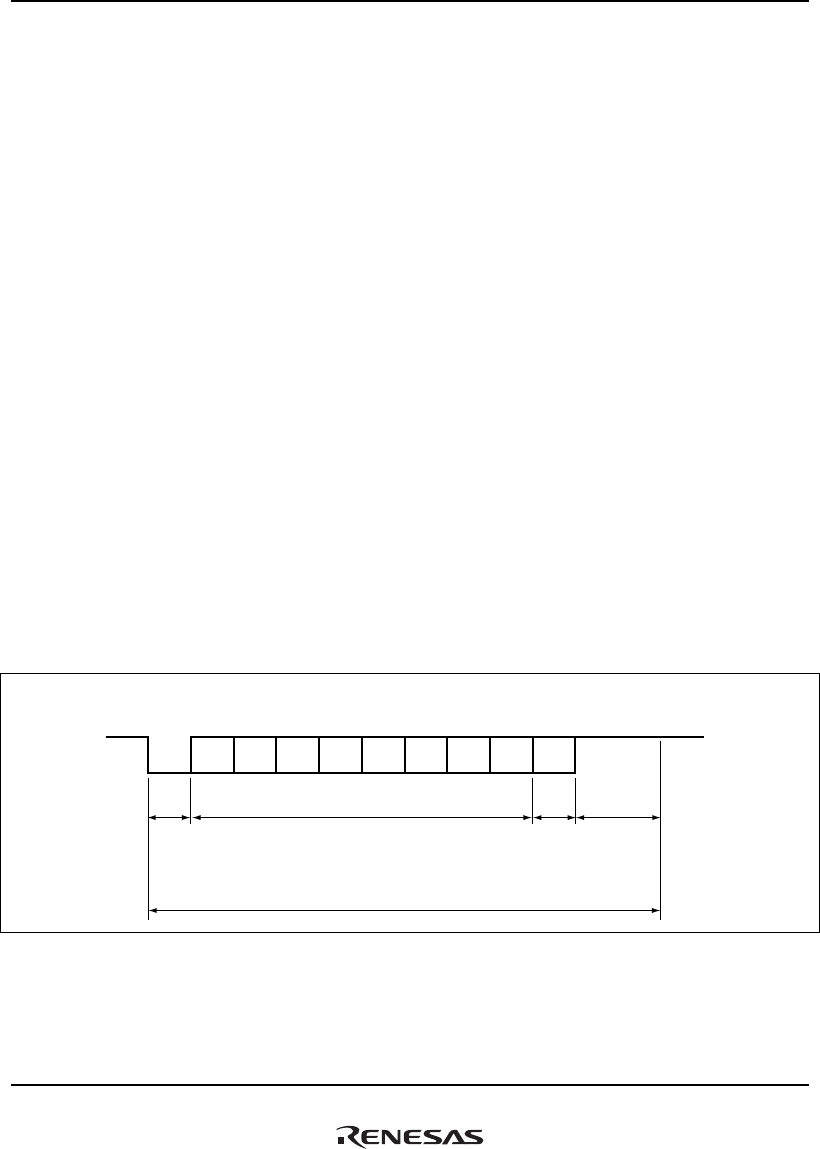
21. Serial Communication Interface with FIFO (SCIF)
Rev.1.00 Jan. 10, 2008 Page 1074 of 1658
REJ09B0261-0100
21.4.2 Operation in Asynchronous Mode
In asynchronous mode, a character that consists of data with a start bit indicating the start of
communication and a stop bit indicating the end of communication is transmitted or received. In
this mode, serial communication is performed with synchronization achieved character by
character.
Inside the SCIF, the transmitter and receiver are independent units, enabling full-duplex
communication. Both the transmitter and receiver have a 64-stage FIFO buffer structure, so that
data can be read or written during transmission or reception, enabling continuous data
transmission and reception.
Figure 21.7 shows the general format for asynchronous serial communication.
In asynchronous serial communication, the transmission line is usually held in the mark state (high
level). The SCIF monitors the transmission line, and when it goes to the space state (low level),
recognizes a start bit and starts serial communication.
One character in serial communication consists of a start bit (low level), followed by
transmit/receive data (LSB first; from the lowest bit), a parity bit (high or low level), and finally
stop bits (high level).
In reception in asynchronous mode, the SCIF synchronizes with the fall of the start bit. Receive
data can be latched at the middle of each bit because the SCIF samples data at the eighth clock
with frequency of 16 times the bit rate.
LSB
Start
bit
MSB
Idle state
(mark state)
Idle state
(mark state)
Stop bit
0
Transmit/receive data
D0 D1 D2 D3 D4 D5 D6 D7 0/1 1 1
11
Serial
data
Parity
bit
1 bit 1 or 2 bits7 or 8 bits 1 bit or
none
One unit of transfer data (character or frame)
Figure 21.7 Data Format in Asynchronous Communication
(Example with 8-Bit Data, Parity, and Two Stop Bits)
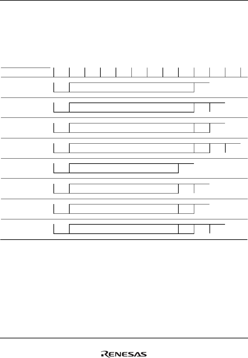
21. Serial Communication Interface with FIFO (SCIF)
Rev.1.00 Jan. 10, 2008 Page 1075 of 1658
REJ09B0261-0100
(1) Data Transfer Format
Table 21.6 shows the data transfer formats that can be used. Any of 8 transfer formats can be
selected according to the SCSMR settings.
Table 21.6 Serial Transfer Formats (Asynchronous Mode)
SCSMR Settings Serial Transfer Format and Frame Length
CHR PE STOP 1 2 3 4 5 6 7 8 9 10 11 12
0 0 0 S 8-bit data STOP
0 0 1 S 8-bit data STOP STOP
0 1 0 S 8-bit data P STOP
0 1 1 S 8-bit data P STOP STOP
1 0 0 S 7-bit data STOP
1 0 1 S 7-bit data STOP STOP
1 1 0 S 7-bit data P STOP
1 1 1 S 7-bit data P STOP STOP
Legend:
S: Start bit
STOP: Stop bit
P: Parity bit

21. Serial Communication Interface with FIFO (SCIF)
Rev.1.00 Jan. 10, 2008 Page 1076 of 1658
REJ09B0261-0100
(2) Clock
Either an internal clock generated by the on-chip baud rate generator or an external clock input at
the SCIF_SCK pin can be selected as the SCIF's serial clock, according to the settings of the C/A
bit in SCSMR and the CKE1 and CKE0 bits in SCSCR. For details on SCIF clock source
selection, see table 21.5.
When an external clock is input to the SCIF_SCK pin, the clock frequency should be 16 times the
bit rate used.
When the SCIF is operated on an internal clock, a clock with frequency of 16 times the bit rate is
output from the SCIF_SCK pin.
(3) SCIF Initialization (Asynchronous Mode)
Before transmitting and receiving data, it is necessary to clear the TE and RE bits in SCSCR to 0,
then initialize the SCIF as described below.
When the operating mode or transfer format, etc., is changed, the TE and RE bits must be cleared
to 0 before making the change using the following procedure.
1. When the TE bit is cleared to 0, SCTSR is initialized. Note that clearing the TE and RE bits to
0 does not change the contents of SCFSR, SCFTDR, or SCFRDR.
2. The TE bit should be cleared to 0 after all transmit data has been sent and the TEND flag in
SCFSR has been set. The TE bit can also be cleared to 0 during transmission, but the data
being transmitted goes to the mark state after the clearance. Before setting TE again to start
transmission, the TFRST bit in SCFCR should first be set to 1 to reset SCFTDR.
3. When an external clock is used, the clock should not be stopped during operation, including
initialization, since operation will be unreliable in this case.
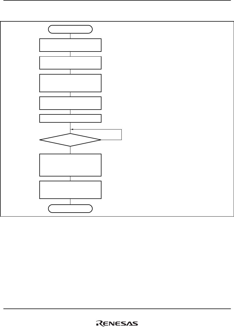
21. Serial Communication Interface with FIFO (SCIF)
Rev.1.00 Jan. 10, 2008 Page 1077 of 1658
REJ09B0261-0100
Figure 21.8 shows a sample SCIF initialization flowchart.
Start of initialization
Clear TE and RE bits in
SCSCR to 0
Set TFCL and RFCL bits in
SCFCR to 1
Set CKE1 and CKE0 bits
in SCSCR (leaving TIE, RIE,
TE, and RE bits cleared to 0)
Set data transfer format
in SCSMR
Set value in SCBRR
1-bit interval elapsed?
Set RTRG1 and RTRG0,
TTRG1 and TTRG0, and
MCE bits in SCFCR, and
clear TFCL and RFCL bits to 0
Set TE and RE bits in
SCSCR to 1, and set TIE, RIE,
and REIE bits
End of initialization
Wait
No
Yes
Set the clock selection in SCSCR.
Be sure to clear bits TIE, RIE, TE,
and RE to 0.
Set the data transfer format in
SCSMR.
Write a value corresponding to the
bit rate into SCBRR. (Not
necessary if an external clock is
used.)
Wait at least one bit interval, then
set the TE bit or RE bit in SCSCR
to 1. Also set the TIE, RIE, and
REIE bits.
Setting the TE and RE bits
enables the SCIF_TXD and
SCIF_RXD pins to be used.
When transmitting, the SCIF goes
to the mark state; when receiving,
it goes to the idle state, waiting for
a start bit.
[1]
[1]
[2]
[3]
[4]
[2]
[3]
[4]
Figure 21.8 Sample SCIF Initialization Flowchart
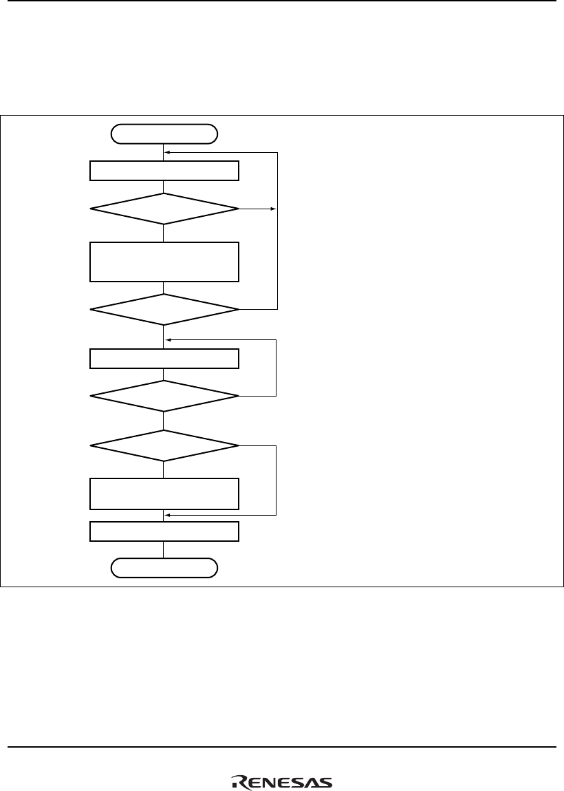
21. Serial Communication Interface with FIFO (SCIF)
Rev.1.00 Jan. 10, 2008 Page 1078 of 1658
REJ09B0261-0100
(4) Serial Data Transmission (Asynchronous Mode)
Figure 21.9 shows a sample flowchart for serial transmission.
Use the following procedure for serial data transmission after enabling the SCIF for transmission.
Start of transmission
Read TDFE flag in SCFSR
TDFE = 1?
Write transmit data in SCFTDR,
and clear TDFE and TEND bits
in SCFSR to 0
All data transmitted?
Read TEND bit in SCFSR
TEND = 1?
Break output?
Clear SPB2DT to 0 and
set SPB2IO to 1
Clear TE bit in SCSCR to 0
End of transmission
No
Yes
No
Yes
No
Yes
No
Yes
[1] SCIF status check and transmit data
write:
Read SCFSR and check that the
TDFE flag is set to 1, then write
transmit data to SCFTDR, and clear
the TDFE and TEND flags to 0.
The number of transmit data bytes
that can be written is 64 - (transmit
trigger setting count).
[2] Serial transmission continuation
procedure:
To continue serial transmission, read
1 from the TDFE flag to confirm that
writing is possible, then write data to
SCFTDR, and then clear the TDFE
flag to 0.
[3] Break output at the end of serial
transmission:
To output a break in serial
transmission, clear the SPB2DT bit to
0 and set the SPB2IO bit to 1 in
SCSPTR, then clear the TE bit in
SCSCR to 0.
In [1] and [2], it is possible to
ascertain the number of data bytes
that can be written from the number
of transmit data bytes in SCFTDR
indicated by SCTFDR.
[1]
[2]
[3]
Figure 21.9 Sample Serial Transmission Flowchart

21. Serial Communication Interface with FIFO (SCIF)
Rev.1.00 Jan. 10, 2008 Page 1079 of 1658
REJ09B0261-0100
In serial transmission, the SCIF operates as follows.
1. When data is written to SCFTDR, the SCIF transfers the data from SCFTDR to SCTSR and
starts transmission. Confirm that the TDFE flag in SCFSR is set to 1 before writing transmit
data to SCFTDR. The number of data bytes that can be written is at least 64 − (transmit trigger
setting count).
2. When data is transferred from SCFTDR to SCTSR and transmission is started, consecutive
transmit operations are performed until there is no transmit data left in SCFTDR. When the
number of transmit data bytes in SCFTDR falls to or below the transmit trigger count set in
SCFCR, the TDFE flag is set. If the TIE bit in SCSCR is set to 1 at this time, a transmit-FIFO-
data-empty interrupt (TXI) request is generated.
The serial transmit data is sent from the SCIF_TXD pin in the following order.
(a) Start bit: One 0-bit is output.
(b) Transmit data: 8-bit or 7-bit data is output in LSB-first order.
(c) Parity bit: One parity bit (even or odd parity) is output. A format in which a parity bit is not
output can also be selected.
(d) Stop bit(s): One or two 1-bits (stop bits) are output.
(e) Mark state: 1 is output continuously until the start bit that starts the next transmission is
sent.
3. The SCIF checks the SCFTDR transmit data at the timing for sending the stop bit. If data is
present, the data is transferred from SCFTDR to SCTSR, the stop bit is sent, and then serial
transmission of the next frame is started.
If there is no transmit data after the stop bit is sent, the TEND flag in SCFSR is set to 1, and
then the SCIF goes to the mark state in which 1 is output from the SCIF_TXD pin.
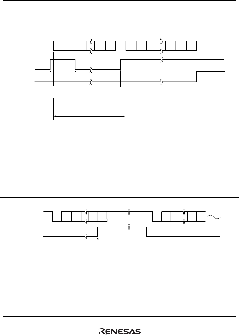
21. Serial Communication Interface with FIFO (SCIF)
Rev.1.00 Jan. 10, 2008 Page 1080 of 1658
REJ09B0261-0100
Figure 21.10 shows an example of the operation for transmission in asynchronous mode.
1
0 D0 D1 D7 0/1 1 0 D0 D1 D7 0/1 1
1
TDFE
TEND
Serial
data
Start
bit
Data Parity
bit
Stop
bit
Start
bit
Idle state
(mark state)
Idle state
(mark state)
SCIF_TXD
Data Parity
bit
Stop
bit
TXI interrupt
request Data written to SCFTDR
and TDFE read as 1 then
cleared to 0 by TXI
interrupt handler
TXI interrupt
request
One frame
Figure 21.10 Example of SCIF Transmission Operation
(Example with 8-Bit Data, Parity, One Stop Bit)
4. When modem control is enabled, transmission can be stopped and restarted in accordance with
the SCIF_CTS input value. When SCIF_CTS is set to 1 during transmission, the SCIF goes to
the mark state after transmission of one frame. When SCIF_CTS is set to 0, the next transmit
data is output starting from the start bit.
Figure 21.11 shows an example of the operation when modem control is used.
Serial data
SCIF_TXD
SCIF_CTS
0 D0 D1 D7 0/1 0 D0 D1 D7 0/1
Drive high before stop bit
Start
bit
Parity
bit
Stop
bit
Start
bit
Figure 21.11 Example of Operation Using Modem Control (SCIF_CTS)
(Only in Channel 0)
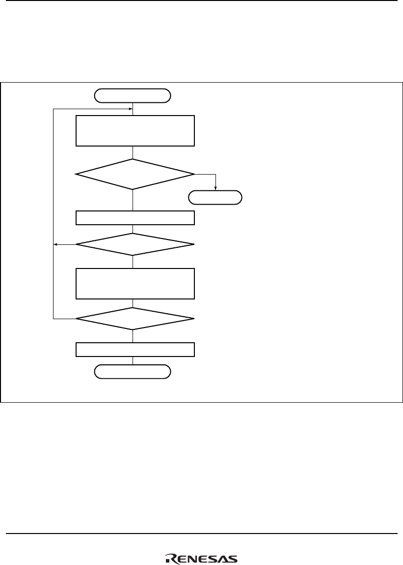
21. Serial Communication Interface with FIFO (SCIF)
Rev.1.00 Jan. 10, 2008 Page 1081 of 1658
REJ09B0261-0100
(5) Serial Data Reception (Asynchronous Mode)
Figure 21.12 shows a sample flowchart for serial reception.
Use the following procedure for serial data reception after enabling the SCIF for reception.
Start of reception
Read ER, DR, BRK flags in
SCFSR and ORER
flag in SCLSR
ER or DR or BRK or ORER = 1?
Read RDF flag in SCFSR
RDF = 1?
Read receive data in
SCFRDR, and clear RDF
flag in SCFSR to 0
All data received?
Clear RE bit in SCSCR to 0
End of reception
Yes
No
Yes
Yes
No
No
Error handling
[1] Receive error handling and
break detection:
Read the DR, ER, and BRK
flags in SCFSR, and the
ORER flag in SCLSR, to
identify any error, perform the
appropriate error handling,
then clear the DR, ER, BRK,
and ORER flags to 0. In the
case of a framing error, a
break can also be detected by
reading the value of the
SCIF_RXD pin.
[2] SCIF status check and receive
data read:
Read SCFSR and check that
RDF = 1, then read the receive
data in SCFRDR, read 1 from
the RDF flag, and then clear
the RDF flag to 0. The
transition of the RDF flag from
0 to 1 can also be identified by
an RXI interrupt.
[3] Serial reception continuation
procedure:
To continue serial reception,
read at least the receive
trigger setting count of receive
data bytes from SCFRDR,
read 1 from the RDF flag, then
clear the RDF flag to 0. The
number of receive data bytes
in SCFRDR can be
ascertained by reading from
SCRFDR.
[1]
[2]
[3]
Figure 21.12 Sample Serial Reception Flowchart (1)
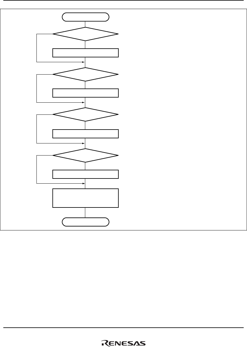
21. Serial Communication Interface with FIFO (SCIF)
Rev.1.00 Jan. 10, 2008 Page 1082 of 1658
REJ09B0261-0100
Error handling
Receive error handling
ER = 1?
BRK = 1?
Break handling
DR = 1?
Read receive data in SCFRDR
Clear DR, ER, BRK flags
in SCFSR,
and ORER flag in SCLSR, to 0
End
Yes
Yes
Yes
No
Overrun error handling
ORER = 1?
Yes
No
No
No
[1] Whether a framing error or parity error
has occurred in the receive data that
is to be read from SCFRDR can be
ascertained from the FER and PER
bits in SCFSR.
[2] When a break signal is received,
receive data (H'00) is not transferred
to SCFRDR.
However, note that the last data in
SCFRDR is H'00, and the break data
in which a framing error occurred is
stored.
When a break handling is completed
and a receive signal returns to 1, the
receive data transfer resumes.
Figure 21.12 Sample Serial Reception Flowchart (2)
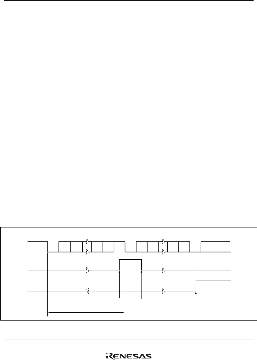
21. Serial Communication Interface with FIFO (SCIF)
Rev.1.00 Jan. 10, 2008 Page 1083 of 1658
REJ09B0261-0100
In serial reception, the SCIF operates as follows.
1. The SCIF monitors the transmission line, and if a 0-start bit is detected, performs internal
synchronization and starts reception.
2. The received data is stored in SCRSR in LSB-to-MSB order.
3. The parity bit and stop bit are received.
After receiving these bits, the SCIF carries out the following checks.
(a) Stop bit check: The SCIF checks whether the stop bit is 1. If there are two stop bits, only
the first is checked.
(b) The SCIF checks whether receive data can be transferred from SCRSR to SCFRDR.*
(c) Overrun error check: The SCIF checks that the ORER flag is 0, indicating that no overrun
error has occurred.*
(d) Break check: The SCIF checks that the BRK flag is 0, indicating that the break state is not
set.*
If (b), (c), and (d) checks are passed, the receive data is stored in SCFRDR.
Note: * Reception continues even when a parity error or framing error occurs.
4. If the RIE bit in SCSCR is set to 1 when the RDF or DR flag changes to 1, a receive-FIFO-
data-full interrupt (RXI) request is generated.
If the RIE bit or REIE bit in SCSCR is set to 1 when the ER flag changes to 1, a receive-error
interrupt (ERI) request is generated.
If the RIE bit or REIE bit in SCSCR is set to 1 when the BRK or ORER flag changes to 1, a
break reception interrupt (BRI) request is generated.
Figure 21.13 shows an example of the operation for reception in asynchronous mode.
1
0 D0 D1 D7 0/1 1 0 D0 D1 D7 0/1 0/10
RDF
FER
Framing error
detected
Serial
data
SCIF_RXD
Start
bit
Data Parity
bit
Stop
bit
Start
bit
Data Parity
bit
Stop
bit
RXI interrupt
request
One frame
Data read and RDF flag
read as 1 then cleared to
0 by RXI interrupt handler
ERI interrupt request
generated by receive
error
Figure 21.13 Example of SCIF Receive Operation
(Example with 8-Bit Data, Parity, One Stop Bit)
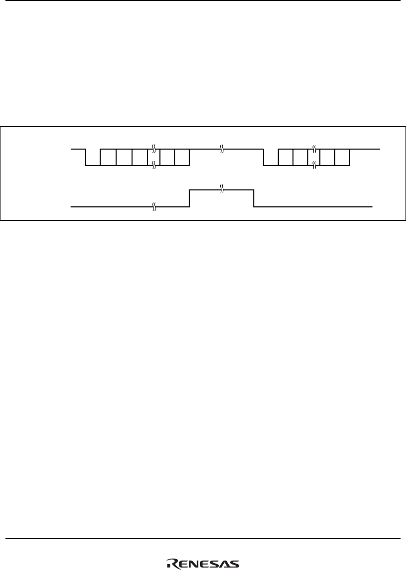
21. Serial Communication Interface with FIFO (SCIF)
Rev.1.00 Jan. 10, 2008 Page 1084 of 1658
REJ09B0261-0100
5. When modem control is enabled, the SCIF_RTS signal is output when SCFRDR is empty.
When SCIF_RTS is 0, reception is possible. When SCIF_RTS is 1, this indicates that
SCFRDR contains bytes of data equal to or more than the SCIF_RTS output active trigger
count. The SCIF_RTS output active trigger value is specified by bits 10 to 8 in SCFCR. For
details, see section 21.3.9, FIFO Control Register n (SCFCR). In addition, SCIF_RTS is also 1
when the RE bit in SCSCR is cleared to 0.
Figure 21.14 shows an example of the operation when modem control is used.
D0 D1 D2 D7 0/1 1 00
Serial data
SCIF_RXD
SCIF_RTS
Start
bit
Parity
bit
Stop
bit
Start
bit
Figure 21.14 Example of Operation Using Modem Control (SCIF_RTS)
(Only in Channels 1 and 2)
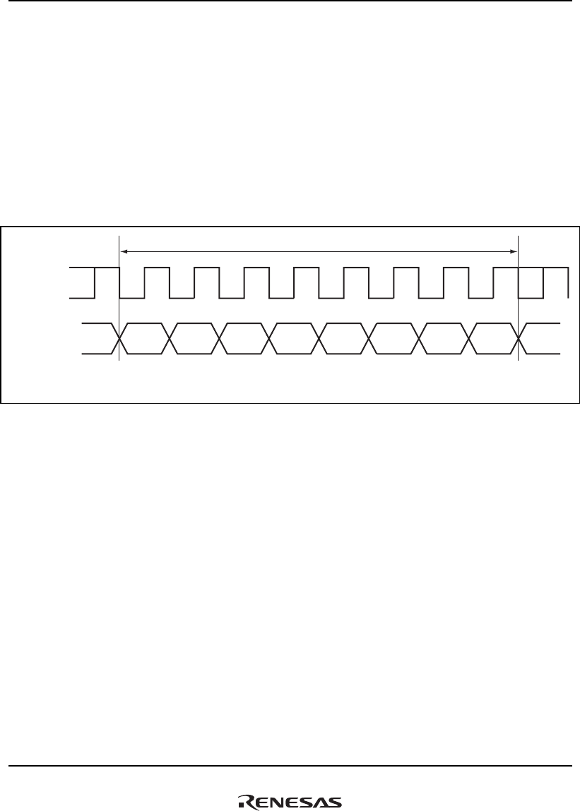
21. Serial Communication Interface with FIFO (SCIF)
Rev.1.00 Jan. 10, 2008 Page 1085 of 1658
REJ09B0261-0100
21.4.3 Operation in Clocked Synchronous Mode
Clocked synchronous mode, in which data is transmitted or received in synchronization with clock
pulses, is suitable for fast serial communication.
Since the transmitter and receiver are independent units in the SCIF, full-duplex communication
can be performed by sharing the clock. Both the transmitter and receiver have a 64-stage FIFO
buffer structure, so that data can be read or written during transmission or reception, enabling
continuous data transmission or reception.
Figure 21.15 shows the general format for clocked synchronous communication.
One unit of transfer data (character or frame)
* *
Bit 0 Bit 1 Bit 2 Bit 3 Bit 4 Bit 5 Bit 6 Bit 7
Don't careDon't care
LSB MSB
Synchronization
clock
Serial data
Note: * High except in continuous transfer
Figure 21.15 Data Format in Clocked Synchronous Communication
In clocked synchronous serial communication, data on the communication line is output from one
fall of the synchronization clock to the next fall. Data is guaranteed to be accurate at the start of
the synchronization clock.
In serial communication, each character is output starting with the LSB and ending with the MSB.
After the MSB is output, the communication line remains in the state of the last data.
In clocked synchronous mode, the SCIF receives data in synchronization with the rise of the
synchronization clock.

21. Serial Communication Interface with FIFO (SCIF)
Rev.1.00 Jan. 10, 2008 Page 1086 of 1658
REJ09B0261-0100
(1) Data Transfer Format
A fixed 8-bit data format is used. No parity bit can be added.
(2) Clock
Either an internal clock generated by the on-chip baud rate generator or an external
synchronization clock input at the SCIF_SCK pin can be selected as the SCIF's serial clock,
according to the settings of the C/A bit in SCSMR and the CKE1 and CKE0 bits in SCSCR. For
details on SCIF clock source selection, see table 21.5.
When the SCIF is operated on an internal clock, the synchronization clock is output from the
SCIF_SCK pin. Eight synchronization clock pulses are output in the transfer of one character, and
when no transfer is performed, the clock is fixed high. When an internal clock is selected in a
receive operation only, as long as the RE bit in SCSCR is set to 1, clock pulses are output until the
number of receive data bytes in the receive FIFO data register reaches the receive trigger count.
(3) SCIF Initialization (Clocked Synchronous Mode)
Before transmitting and receiving data, it is necessary to clear the TE and RE bits in SCSCR to 0,
then initialize the SCIF as described below.
When changing the operating mode or transfer format, etc., the TE and RE bits must be cleared to
0 before making the change using the following procedure. When the TE bit is cleared to 0,
SCTSR is initialized. Note that clearing the RE bit to 0 does not initialize the RDF, PER, FER, or
ORER flag state or change the contents of SCFRDR.
Figure 21.16 shows a sample SCIF initialization flowchart.
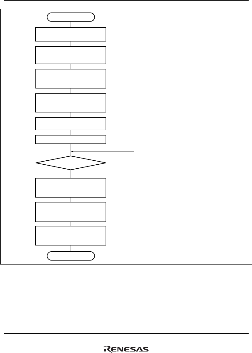
21. Serial Communication Interface with FIFO (SCIF)
Rev.1.00 Jan. 10, 2008 Page 1087 of 1658
REJ09B0261-0100
Start of initialization
Clear TE and RE bits
in SCSCR to 0
Set TFCL and RFCL bits
in SCFCR to 1 to clear
the FIFO buffer
After reading BRK, DR,
and ER flags in SCFSR,
write 0 to clear them
Set CKE1 and CKE0 bits
in SCSCR (leaving TE, RE, TIE,
and RIE bits cleared to 0)
Set data transfer format
in SCSMR
Set value in SCBRR
1-bit interval elapsed?
Set RTRG1 and RTRG0 and
TTRG1 and TTRG0 bits in SCFCR,
and clear TFCL and RFCL bits to 0
Set TE and RE bits in SCSCR
to 1, and set TIE, RIE,
and REIE bits
Set external pins to be used
(SCIF_CLK, SCIF_TXD,
and SCIF_RXD)
End of initialization
Wait
No
Yes
Leave the TE and RE bits cleared
to 0 until the initialization almost
ends. Be sure to clear the TIE,
RIE, TE, and RE bits to 0.
Set the CKE1 and CKE0 bits.
Set the data transfer format in
SCSMR.
Write a value corresponding to
the bit rate into SCBRR. This
is not necessary if an external
clock is used. Wait at least one
bit interval after this write before
moving to the next step.
Set the external pins to be used.
Set SCIF_RXD input for reception and
SCIF_TXD output for transmission.
The input/output of the SCIF_CLK pin
must match the setting of the CKE1
and CKE0 bits.
Set the TE or RE bit in SCSCR
to 1. Also set the TIE, RIE, and
REIE bits to enable the SCIF_TXD,
SCIF_RXD, and SCIF_CLK pins to
be used. When transmitting, the
SCIF_TXD pin goes to the mark
state. When receiving in clocked
synchronous mode with the
synchronization clock output (clock
master) selected, a clock starts to
be output from the SCIF_CLK pin
at this point.
[1]
[1]
[2]
[3]
[4]
[5]
[6]
[2]
[3]
[4]
[5]
[6]
Figure 21.16 Sample SCIF Initialization Flowchart
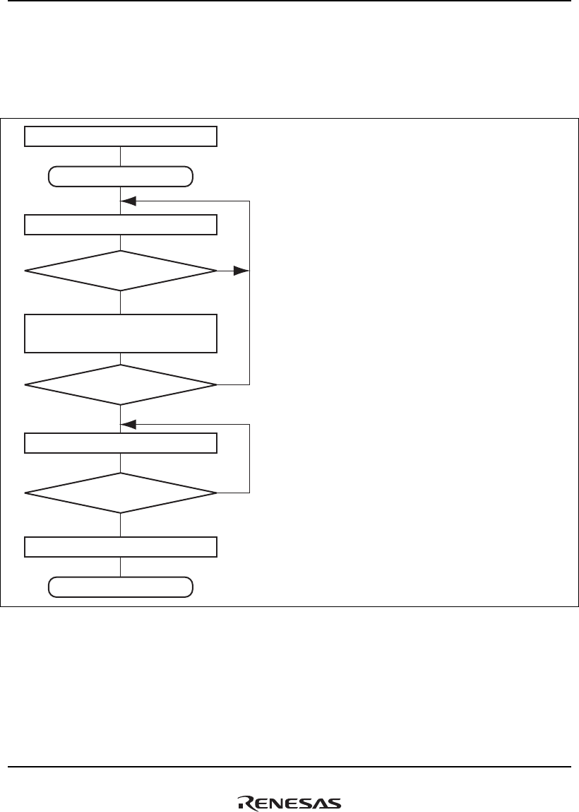
21. Serial Communication Interface with FIFO (SCIF)
Rev.1.00 Jan. 10, 2008 Page 1088 of 1658
REJ09B0261-0100
(4) Serial Data Transmission (Clocked Synchronous Mode)
Figure 21.17 shows a sample flowchart for serial transmission.
Use the following procedure for serial data transmission after enabling the SCIF for transmission.
Start of transmission
Initialization
Read TDFE bit in SCFSR
TDFE = 1 ?
All data transmitted?
Read TEND flag in SCFSR
TEND = 1 ?
Clear TE bit in SCSCR to 0
End of transmission
[1] SCIF initialization:
See Sample SCIF Initialization Flowchart in figure
21.16.
[2] SCIF status check and transmit data write:
Read SCFSR and check that the TDFE flag is set to
1, then write transmit data to SCFTDR, and clear
the TDFE flag to 0. The transition of the TDFE flag
from 0 to 1 can also be identified by a TXI interrupt.
[3] Serial transmission continuation procedure:
To continue serial transmission, read 1 from the
TDFE flag to confirm that writing is possible, then
write data to SCFTDR, and then clear the TDFE
flag to 0.
[1]
[2]
[3]
Ye s
No
No
No
Ye s
Ye s
Write transmit data to SCFTDR and clear
TDFE and TEND bits in SCFSR to 0
Figure 21.17 Sample Serial Transmission Flowchart

21. Serial Communication Interface with FIFO (SCIF)
Rev.1.00 Jan. 10, 2008 Page 1089 of 1658
REJ09B0261-0100
In serial transmission, the SCIF operates as follows.
1. When data is written into SCFTDR, the SCIF transfers the data from SCFTDR to SCTSR and
starts transmitting. Confirm that the TDFE flag in SCFSR is set to 1 before writing transmit
data to SCFTDR. The number of data bytes that can be written is at least 64 (transmit trigger
setting count).
2. When data is transferred from SCFTDR to SCTSR and transmission is started, consecutive
transmit operations are performed until there is no transmit data left in SCFTDR. When the
number of transmit data bytes in SCFTDR falls to or below the transmit trigger count set in
SCFCR, the TDFE flag is set. If the TIE bit in SCSCR is set to 1 at this time, a transmit-FIFO-
data-empty interrupt (TXI) request is generated.
If clock output mode is selected, the SCIF outputs eight synchronization clock pulses for each
data.
When the external clock is selected, data is output in synchronization with the input clock.
The serial transmit data is sent from the SCIF_TXD pin in LSB-first order.
3. The SCIF checks the SCFTDR transmit data at the timing for sending the last bit. If data is
present, the data is transferred from SCFTDR to SCTSR, and then serial transmission of the
next frame is started. If there is no transmit data, the TEND flag in SCFSR is set to 1 after the
last bit is sent, and the transmit data pin (SCIF_TXD pin) retains the output state of the last bit.
4. After serial transmission ends, the SCIF_SCK pin is fixed high when the CKE1 bit in SCSCR
is 0.
Figure 21.18 shows an example of the SCIF transmission operation.
Bit 0 Bit 1 Bit 7 Bit 0 Bit 1 Bit 6 Bit 7
TXI interrupt
request
Data written to SCFTDR
and TDFE flag cleared to 0
by TXI interrupt handler
LSB
TDFE
TEND
MSB
TXI interrupt
request
Synchronization
clock
SCIF_SCK
Serial data
SCIF_TXD
One frame
Figure 21.18 Example of SCIF Transmission Operation
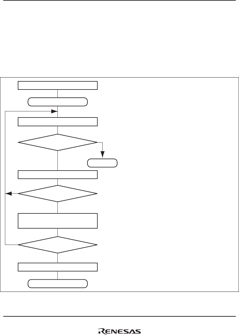
21. Serial Communication Interface with FIFO (SCIF)
Rev.1.00 Jan. 10, 2008 Page 1090 of 1658
REJ09B0261-0100
(5) Serial Data Reception (Clocked Synchronous Mode)
Figure 21.19 shows a sample flowchart for serial reception.
Use the following procedure for serial data reception after enabling the SCIF for reception.
When switching the operating mode from asynchronous mode to clocked synchronous mode
without initializing the SCIF, make sure that the ORER, PER7 to PER0, and FER7 to FER0 flags
are cleared to 0.
Read receive data in SCFRDR, and
clear RDF flag in SCFSR to 0
Start of reception
Initialization
Read ORER flag in SCLSR
ORER = 1 ?
Read RDF flag in SCFSR
RDF = 1 ?
All data received?
Clear RE bit in SCSCR to 0
End of reception
[1] SCIF initialization:
See Sample SCIF Initialization Flowchart in figure
21.16.
[2] Receive error handling:
Read the ORER flag in SCLSR to identify any error,
perform the appropriate error handling, then clear the
ORER flag to 0.
Transmission/reception cannot be resumed while the
ORER flag is set to 1.
[3] SCIF status check and receive data read:
Read SCFSR and check that RDF = 1, then read the
receive data in SCFRDR, and clear the RDF flag to
0. The transition of the RDF flag from 0 to 1 can also
be identified by an RXI interrupt.
[4] Serial reception continuation procedure:
To continue serial reception, read at east the receive
trigger setting count of receive data bytes from
SCFRDR, read 1 from the RDF flag, then clear the
RDF flag to 0. The number of receive data bytes in
SCFRDR can be ascertained by reading SCRFDR.
[1]
[2]
[3]
[4]
Ye s
Ye s
No
No
No
Ye s
Error handling
Figure 21.19 Sample Serial Reception Flowchart (1)
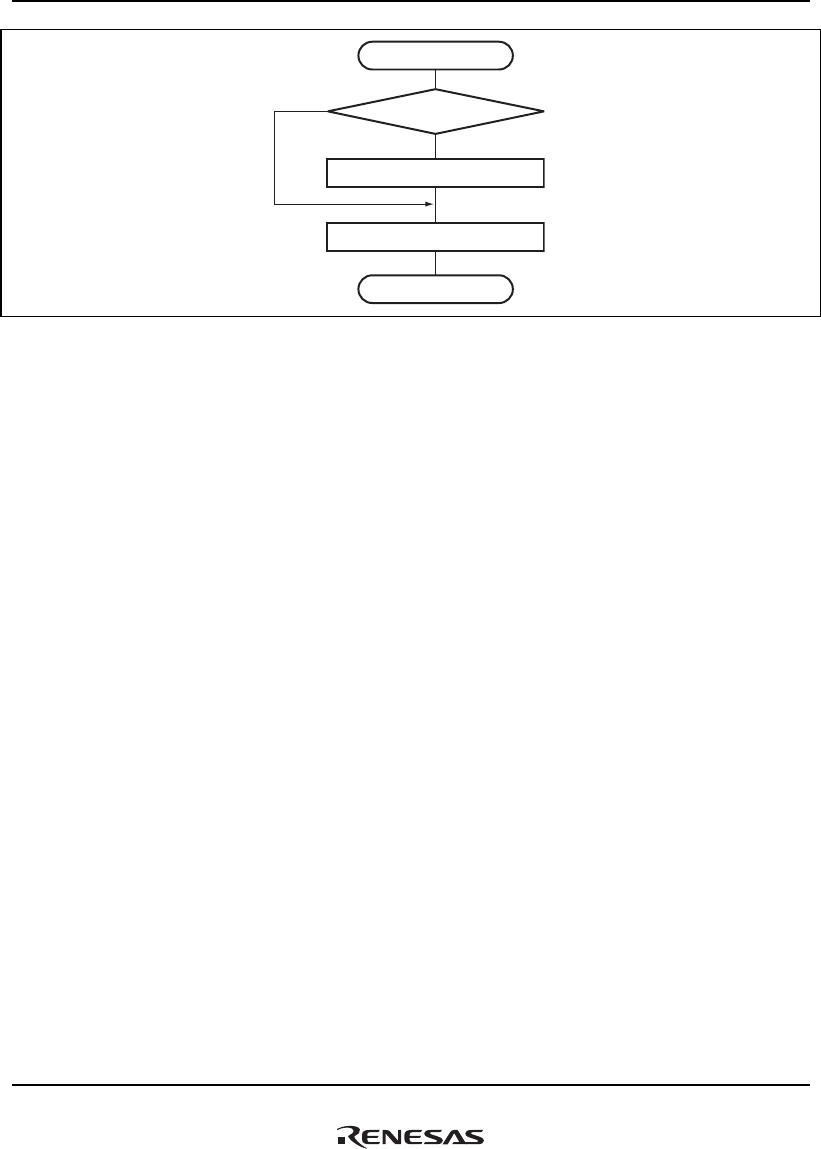
21. Serial Communication Interface with FIFO (SCIF)
Rev.1.00 Jan. 10, 2008 Page 1091 of 1658
REJ09B0261-0100
Error handling
Clear ORER flag in SCLSR to 0
End
Overrun error handling
ORER = 1?
Yes
No
Figure 21.19 Sample Serial Reception Flowchart (2)
In serial reception, the SCIF operates as follows.
1. The SCIF is initialized internally in synchronization with the input or output of the
synchronization clock.
2. The receive data is stored in SCRSR in LSB-to-MSB order.
After receiving the data, the SCIF checks whether the receive data can be transferred from
SCRSR to SCFRDR. If this check is passed, the receive data is stored in SCFRDR. If an
overrun error is detected in the error check, reception cannot continue.
3. If the RIE bit in SCSCR is set to 1 when the RDF flag changes to 1, a receive-FIFO-data-full
interrupt (RXI) request is generated.
If the RIE bit in SCSCR is set to 1 when the ORER flag changes to 1, a break interrupt (BRI)
request is generated.
Figure 21.20 shows an example of the SCIF reception operation.
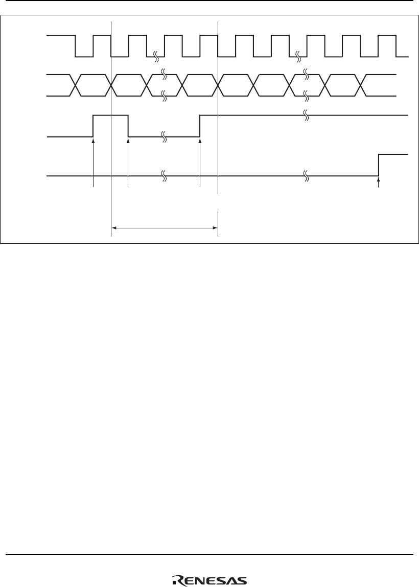
21. Serial Communication Interface with FIFO (SCIF)
Rev.1.00 Jan. 10, 2008 Page 1092 of 1658
REJ09B0261-0100
Bit 7 Bit 0 Bit 7 Bit 0 Bit 1 Bit 6 Bit 7
RXI interrupt
request
One frame
Data read from
SCFRDR and RDF flag
cleared to 0 by RXI
interrupt handler
LSB
RDF
Serial data
SCIF_RXD
Synchronization
clock
ORER
MSB
RXI interrupt
request
BRI interrupt request
by overrun error
Figure 21.20 Example of SCIF Reception Operation
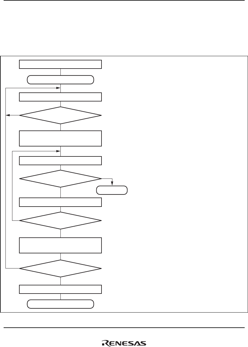
21. Serial Communication Interface with FIFO (SCIF)
Rev.1.00 Jan. 10, 2008 Page 1093 of 1658
REJ09B0261-0100
(6) Transmitting and Receiving Serial Data Simultaneously (Clocked Synchronous Mode)
Figure 21.21 shows a sample flowchart for transmitting and receiving data simultaneously.
Use the following procedure for the simultaneous serial transmission/reception of serial data, after
enabling the SCIF transmission/reception.
Read receive data in SCFRDR, and
clear RDF flag in SCFSR to 0
Write transmit data to SCFTDR, and
clear TDFE flag in SCFSR to 0
Start of transmission and reception
Initialization
Read TDFE flag in SCFSR
TDFE = 1 ?
Read ORER flag in SCLSR
ORER = 1 ?
Read RDF flag in SCFSR
RDF = 1 ?
All data received?
Clear TE and RE bits in SCSCR to 0
End of transmission and reception
[1] SCIF initialization:
See Sample SCIF Initialization Flowchart in figure
21.16.
[2] SCIF status check and transmit data write:
Read SCFSR and check that the TDFE flag is set to 1,
then write transmit data to SCFTDR, and clear the
TDFE flag to 0. The transition of the TDFE flag from 0
to 1 can also be identified by a TXI interrupt.
[3] Receive error handling:
Read the ORER flag in SCLSR to identify any error,
perform the appropriate error handling, then clear the
ORER flag to 0. Reception cannot be resumed while
the ORER flag is set to 1.
[4] SCIF status check and receive data read:
Read SCFSR and check that RDF = 1, then read the
receive data in SCFRDR, and clear the RDF flag to 0.
The transition of the RDF flag from 0 to 1 can also be
identified by an RXI interrupt.
[5] Serial transmission and reception continuation
procedure:
To continue serial transmission and reception, read
RDF flag and SCFRDR, and clear the RDF flag to 0
before receiving the MSB in the current frame.
Similarly, read 1 from the TDFE flag to confirm that
writing is possible before transmitting the MSB in the
current frame. Then write data to SCFTDR and clear
the TDFE flag to 0.
Note: When switching from a transmit operation or receive
operation to simultaneous transmission and reception
operations, clear the TE and RE bits to 0, and then set
them simultaneously to 1.
[1]
[2]
[3]
[4]
[5]
Ye s
Ye s
Ye s
Ye s
No
No
No
No
Error handling
Figure 21.21 Sample Flowchart for Transmitting/Receiving Serial Data

21. Serial Communication Interface with FIFO (SCIF)
Rev.1.00 Jan. 10, 2008 Page 1094 of 1658
REJ09B0261-0100
21.5 SCIF Interrupt Sources and the DMAC
The SCIF has four interrupt sources for each channel: transmit-FIFO-data-empty interrupt (TXI)
request, receive-error interrupt (ERI) request, receive-FIFO-data-full interrupt (RXI) request, and
break interrupt (BRI) request.
Table 21.7 shows the interrupt sources and their order of priority. The interrupt sources are
enabled or disabled by means of the TIE, RIE, and REIE bits in SCSCR. A separate interrupt
request is sent to the interrupt controller for each of these interrupt sources.
If the TDFE flag in SCFSR is set to 1 when a TXI interrupt is enabled by the TIE bit, a TXI
interrupt request and a transmit-FIFO-data-empty request for DMA transfer are generated. If the
TDFE flag is set to 1 when a TXI interrupt is disabled by the TIE bit, only a transmit-FIFO-data-
empty request for DMA transfer is generated. A transmit-FIFO-data-empty request can activate
the DMAC to perform data transfer.
If the RDF or DR flag in SCFSR is set to 1 when an RXI interrupt is enabled by the RIE bit, an
RXI interrupt request and a receive-FIFO-data-full request for DMA transfer are generated. If the
RDF or DR flag is set to 1 when an RXI interrupt is disabled by the RIE bit, only a receive-FIFO-
data-full request for DMA transfer is generated. A receive-FIFO-data-full request can activate the
DMAC to perform data transfer. Note that generation of an RXI interrupt request or a receive-
FIFO-data-full request by setting the DR flag to 1 occurs only in asynchronous mode.
When the BRK flag in SCFSR or the ORER flag in SCLSR is set to 1, a BRI interrupt request is
generated.
If transmission/reception is carried out using the DMAC, set and enable the DMAC before making
the SCIF setting. Also make settings to inhibit output of RXI and TXI interrupt requests to the
interrupt controller. If output of interrupt requests is enabled, these interrupt requests to the
interrupt controller can be cleared by the DMAC regardless of the interrupt handler.
By setting the REIE bit to 1 while the RIE bit is cleared to 0 in SCSCR, it is possible to output
ERI interrupt requests, but not RXI interrupt requests.

21. Serial Communication Interface with FIFO (SCIF)
Rev.1.00 Jan. 10, 2008 Page 1095 of 1658
REJ09B0261-0100
Table 21.7 SCIF Interrupt Sources
Interrupt
Source Description
DMAC
Activation
Priority on
Reset Release
ERI Interrupt initiated by receive error flag (ER) Not possible High
RXI Interrupt initiated by receive FIFO data full flag
(RDF) or receive data ready flag (DR)*
Possible
BRI Interrupt initiated by break flag (BRK) or overrun
error flag (ORER)
Not possible
TXI Interrupt initiated by transmit FIFO data empty
flag (TDFE)
Possible
Low
Note: * An RXI interrupt by setting of the DR flag is available only in asynchronous mode.

21. Serial Communication Interface with FIFO (SCIF)
Rev.1.00 Jan. 10, 2008 Page 1096 of 1658
REJ09B0261-0100
21.6 Usage Notes
Note the following when using the SCIF.
(1) SCFTDR Writing and the TDFE Flag
The TDFE flag in SCFSR is set when the number of transmit data bytes written in SCFTDR has
fallen to or below the transmit trigger count set by bits TTRG1 and TTRG0 in SCFCR. After
TDFE is set, transmit data up to the number of empty bytes in SCFTDR can be written, allowing
efficient continuous transmission.
However, if the number of data bytes written in SCFTDR is equal to or less than the transmit
trigger count, the TDFE flag will be set to 1 again, even after being read as 1 and cleared to 0.
Therefore, the TDFE flag should be cleared when SCFTDR contains more than the transmit
trigger count of transmit data bytes.
The number of transmit data bytes in SCFTDR can be found from SCTFDR.
(2) SCFRDR Reading and the RDF Flag
The RDF flag in SCFSR is set when the number of receive data bytes in SCFRDR has become
equal to or greater than the receive trigger count set by bits RTRG1 and RTRG0 in SCFCR. After
RDF is set, receive data equivalent to the trigger count can be read from SCFRDR, allowing
efficient continuous reception.
However, if the number of data bytes read in SCFRDR is equal to or greater than the trigger count,
the RDF flag will be set to 1 again even if it is cleared to 0. After the receive data is read, clear the
RDF flag readout to 0 in order to reduce the number of data bytes in SCFRDR to less than the
trigger count.
The number of receive data bytes in SCFRDR can be found from SCRFDR.
(3) Break Detection and Processing
If a framing error (FER) is detected, break signals can also be detected by reading the SCIF_RXD
pin value directly. In the break state the input values from the SCIF_RXD consists of all 0s, so the
FER flag is set and the parity error flag (PER) may also be set.
Although the SCIF stops transferring receive data to SCFRDR after receiving a break, the receive
operation continues.
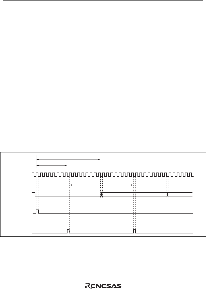
21. Serial Communication Interface with FIFO (SCIF)
Rev.1.00 Jan. 10, 2008 Page 1097 of 1658
REJ09B0261-0100
(4) Sending a Break Signal
The input/output condition and level of the SCIF_TXD pin are determined by bits SPB2IO and
SPB2DT in SCSPTR. This feature can be used to send a break signal.
After the serial transmitter is initialized and until the TE bit is set to 1 (enabling transmission), the
SCIF_TXD pin function is not selected and the value of the SPB2DT bit substitutes for the mark
state. The SPB2IO and SPB2DT bits should therefore be set to 1 (designating output and high
level) in the beginning.
To send a break signal during serial transmission, clear the SPB2DT bit to 0 (designating low
level), and then clear the TE bit to 0 (halting transmission). When the TE bit is cleared to 0, the
transmitter is initialized, regardless of the current transmission state, and 0 is output from the
SCIF_TXD pin.
(5) Receive Data Sampling Timing and Receive Margin in Asynchronous Mode
In asynchronous mode, the SCIF operates on a base clock with frequency of 16 times the bit rate.
In reception, the SCIF synchronizes internally with the fall of the start bit, which it samples on the
base clock. Receive data is latched at the rising edge of the eighth base clock pulse.
Figure 21.22 shows the timing.
0 1 2 3 4 5 6 7 8 9 10 11 12 13 14 15 0 1 2 3 4 5 6 7 8 9 10 11 12 13 14 15 0 1 2 3 4 5
16 clocks
8 clocks
-7.5 clocks
Start bit
+7.5 clocks
D0 D1
Receive data
(SCIF_RXD)
Synchronization
sampling
timing
Data sampling timing
Base clock
Figure 21.22 Receive Data Sampling Timing in Asynchronous Mode

21. Serial Communication Interface with FIFO (SCIF)
Rev.1.00 Jan. 10, 2008 Page 1098 of 1658
REJ09B0261-0100
Thus, the reception margin in asynchronous mode is given by formula (1).
1 | D - 0.5 |
M= (0.5 - 2N ) - (L - 0.5) F - N (1 + F) × 100 % .................. (1)
M: Receive margin (%)
N: Ratio of bit rate to clock (N = 16)
D: Clock duty (D = 0 to 1.0)
L: Frame length (L = 9 to 12)
F: Absolute value of clock rate deviation
From equation (1), if F = 0 and D = 0.5, the reception margin is 46.875%, as given by formula (2).
When D = 0.5 and F = 0:
M = (0.5 – 1 / (2 × 16) ) × 100% = 46.875% ............................................... (2)
However, this is a theoretical value. A reasonable margin to allow in system designs is 20% to
30%.

22. Serial I/O with FIFO (SIOF)
Rev.1.00 Jan. 10, 2008 Page 1099 of 1658
REJ09B0261-0100
Section 22 Serial I/O with FIFO (SIOF)
This LSI is equipped with a clock-synchronized serial I/O module with FIFO (SIOF).
22.1 Features
• Serial transfer
32-bit FIFO × 16-stage (the transmit FIFO and receive FIFO are independent units)
Supports input/output for 8-bit data, 16-bit data, and 16-bit stereo audio data
MSB first for data transmission and reception
Supports up to 48-kHz sampling rate
Synchronization by either frame synchronization pulse or left/right channel switch
Supports CODEC control data interface
Connectable to linear, audio, A-Law, or μ-Law CODEC chip
Supports both master and slave modes
• Serial clock
An external pin input or peripheral clock (Pck) can be selected as the clock source.
• Interrupts: One type
• DMA transfer
Supports DMA transfer by a transfer request from the transmit FIFO unit
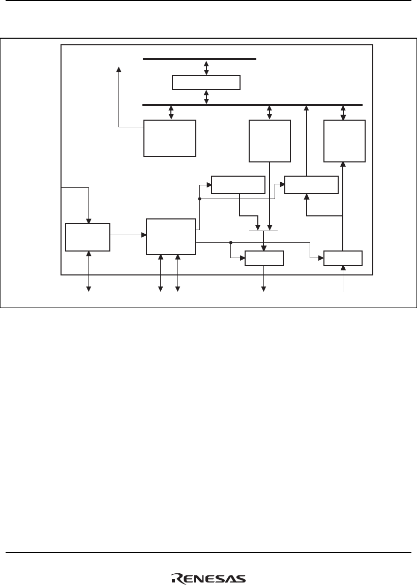
22. Serial I/O with FIFO (SIOF)
Rev.1.00 Jan. 10, 2008 Page 1100 of 1658
REJ09B0261-0100
Figure 22.1 shows a block diagram of the SIOF.
P/S
Transmit
FIFO
(32 bits ×
16 stages)
Pck
1/nMCLK
SIOF_MCLK SIOF_SCK SIOF_SYNC SIOF_TXD SIOF_RXD
SIOF interrupt
request
Bus interface
Control
registers
Baud rate
generator Timing control
Transmit
control data
Peripheral bus
Receive
FIFO
(32 bits ×
16 stages)
Receive
control data
S/P
Figure 22.1 Block Diagram of SIOF

22. Serial I/O with FIFO (SIOF)
Rev.1.00 Jan. 10, 2008 Page 1101 of 1658
REJ09B0261-0100
22.2 Input/Output Pins
Table 22.1 shows the pin configuration.
Table 22.1 Pin Configuration
Pin Name* Function I/O Description
SIOF_MCLK Master clock Input Master clock input pin
SIOF_SCK Serial clock I/O Serial clock pin (common to
transmission/reception)
SIOF_SYNC Frame synchronous
signal
I/O Frame synchronous signal
(common to transmission/reception)
SIOF_TXD Transmit data Output Transmit data pin
SIOF_RXD Receive data Input Receive data pin
Note: * A pin group to be used can be selected according to the setting of PFC.
For details, see Peripheral Module Select Register 1 and Peripheral Module Select
Register 2, in section 28, General Purpose I/O Ports (GPIO).

22. Serial I/O with FIFO (SIOF)
Rev.1.00 Jan. 10, 2008 Page 1102 of 1658
REJ09B0261-0100
22.3 Register Descriptions
Table 22.2 shows the register configuration of the SIOF. Table 22.3 shows the register states in
each operating mode.
Table 22.2 Register Configuration
Name Abbreviation R/W P4 Address Area7 Address
Access
Size
Sync
Clock
Mode register SIMDR R/W H'FFE2 0000 H'1FE2 0000 16 Pck
Clock select register SISCR R/W H'FFE2 0002 H'1FE2 0002 16 Pck
Transmit data assign register SITDAR R/W H'FFE2 0004 H'1FE2 0004 16 Pck
Receive data assign register SIRDAR R/W H'FFE2 0006 H'1FE2 0006 16 Pck
Control data assign register SICDAR R/W H'FFE2 0008 H'1FE2 0008 16 Pck
Control register SICTR R/W H'FFE2 000C H'1FE2 000C 16 Pck
FIFO control register SIFCTR R/W H'FFE2 0010 H'1FE2 0010 16 Pck
Status register SISTR R/W H'FFE2 0014 H'1FE2 0014 16 Pck
Interrupt enable register SIIER R/W H'FFE2 0016 H'1FE2 0016 16 Pck
Transmit data register SITDR W H'FFE2 0020 H'1FE2 0020 32 Pck
Receive data register SIRDR R H'FFE2 0024 H'1FE2 0024 32 Pck
Transmit control data register SITCR R/W H'FFE2 0028 H'1FE2 0028 32 Pck
Receive control data register SIRCR R/W H'FFE2 002C H'1FE2 002C 32 Pck

22. Serial I/O with FIFO (SIOF)
Rev.1.00 Jan. 10, 2008 Page 1103 of 1658
REJ09B0261-0100
Table 22.3 Register States in Each Operating Mode
Name Abbreviation
Power-On
Reset
Manual
Reset
Module
Standby Sleep
Mode register SIMDR H'8000 H'8000 Retained Retained
Clock select register SISCR H'C000 H'C000 Retained Retained
Transmit data assign register SITDAR H'0000 H'0000 Retained Retained
Receive data assign register SIRDAR H'0000 H'0000 Retained Retained
Control data assign register SICDAR H'0000 H'0000 Retained Retained
Control register SICTR H'0000 H'0000 Retained Retained
FIFO control register SIFCTR H'1000 H'1000 Retained Retained
Status register SISTR H'0000 H'0000 Retained Retained
Interrupt enable register SIIER H'0000 H'0000 Retained Retained
Transmit data register SITDR H'xxxx xxxx H'xxxx xxxx Retained Retained
Receive data register SIRDR H'xxxx xxxx H'xxxx xxxx Retained Retained
Transmit control data register SITCR H'0000 0000 H'0000 0000 Retained Retained
Receive control data register SIRCR H'xxxx xxxx H'xxxx xxxx Retained Retained

22. Serial I/O with FIFO (SIOF)
Rev.1.00 Jan. 10, 2008 Page 1104 of 1658
REJ09B0261-0100
22.3.1 Mode Register (SIMDR)
SIMDR is a 16-bit readable/writable register that sets the SIOF operating mode.
01234567891011121315 14
0000000000000010
————
SYN
CDL
SYN
CAC
RCIMTXDIZFL[3:0]REDG
SYN
CAT
TRMD[1:0]
RRRRR/WR/WR/WR/WR/WR/WR/WR/WR/WR/WR/W R/W
BIt:
Initial value:
R/W:
Bit Bit Name
Initial
Value R/W Description
15, 14 TRMD[1:0] 10 R/W Transfer Mode 1, 0
These bits select transfer mode shown in table 22.4.
00: Slave mode 1
01: Slave mode 2
10: Master mode 1
11: Master mode 2
13 SYNCAT 0 R/W SIOF_SYNC Pin Valid Timing
Indicates the position of the SIOF_SYNC signal to be
output as a synchronous pulse.
0: At the start bit data of frame
1: At the last bit data of slot
12 REDG 0 R/W Receive Data Sampling Edge
0: The SIOF_RXD signal is sampled at the falling edge
of SIOF_SCK
1: The SIOF_RXD signal is sampled at the rising edge
of SIOF_SCK
Note: The timing to transmit the SIOF_TXD signal is at
the opposite edge of the timing that samples the
SIOF_RXD. This bit is valid only in master
mode.
11 to 8 FL[3:0] 0000 R/W Frame Length 3 to 0
These bits specify the flame length of transfer data
format. For the correspondence among setting values,
data length, and frame length, see table 22.7.

22. Serial I/O with FIFO (SIOF)
Rev.1.00 Jan. 10, 2008 Page 1105 of 1658
REJ09B0261-0100
Bit Bit Name
Initial
Value R/W Description
7 TXDIZ 0 R/W SIOF_TXD Pin Output when Transmission is Invalid*
0: High output when invalid
1: High-impedance state when invalid
Note: Transmission is invalid when transmission is
disabled, or when a slot that is not assigned as
transmit data or control data is being
transmitted.
6 RCIM 0 R/W Receive Control Data Interrupt Mode
0: Sets the RCRDY bit in SISTR when the contents of
SIRCR change.
1: Sets the RCRDY bit in SISTR each time when
SIRCR receives the control data.
5 SYNCAC 0 R/W SIOF_SYNC Pin Polarity
This bit is valid when the SIOF_SYNC signal is output
as synchronous pulse.
0: Active-high
1: Active-low
4 SYNCDL 0 R/W Data Pin Bit Delay for SIOF_SYNC Pin
This bit is valid when the SIOF_SYNC signal is output
as synchronous pulse. In slave mode, specify one-bit
delay.
0: No bit delay
1: 1-bit delay
3 to 0 ⎯ All 0 R Reserved
These bits are always read as 0. The write value should
always be 0.
Table 22.4 shows the operation in each transfer mode.
Table 22.4 Operation in Each Transfer Mode
Transfer Mode Master/Slave SIOF_SYNC Bit Delay Control Data Method*
Slave mode 1 Slave Synchronous pulse Slot position
Slave mode 2 Slave Synchronous pulse Secondary FS
Master mode 1 Master Synchronous pulse
SYNCDL bit
Slot position
Master mode 2 Master L/R No Not supported
Note: * The control data method is valid when the FL bits are set to 1xxx. (x: don't care.)
For details, see section 22.4.5, Control Data Interface.

22. Serial I/O with FIFO (SIOF)
Rev.1.00 Jan. 10, 2008 Page 1106 of 1658
REJ09B0261-0100
22.3.2 Control Register (SICTR)
SICTR is a 16-bit readable/writable register that sets the SIOF operating state.
01234567891011121315 14
0000000000000000
RXRSTTXRST——————RXETXE————SCKE FSE
R/WR/WRRRRRRR/WR/WRRRRR/W R/W
BIt:
Initial value:
R/W:
Bit Bit Name
Initial
Value R/W Description
15 SCKE 0 R/W Serial Clock Output Enable
This bit is valid in master mode.
0: Disables the SIOF_SCK output (outputs low level)
1: Enables the SIOF_SCK output
If this bit is set to 1, the SIOF initializes the baud rate
generator and initiates the operation. At the same time,
the SIOF outputs the clock generated by the baud rate
generator to the SIOF_SCK pin.
14 FSE 0 R/W Frame Synchronous Signal Output Enable
This bit is valid in master mode.
0: Disables the SIOF_SYNC output (outputs low level)
1: Enables the SIOF_SYNC output
If this bit is set to 1, the SIOF initializes the frame
counter and initiates the operation.
13 to 10 ⎯ All 0 R Reserved
These bits are always read as 0. The write value should
always be 0.
9 TXE 0 R/W Transmit Enable
0: Disables data transmission from the SIOF_TXD pin
(Outputs according to the value set in the TXDIZ bit)
1: Enables data transmission from the SIOF_TXD pin
• This bit setting becomes valid at the start of the next
frame (at the rising edge of the SIOF_SYNC signal).
• When the 1 setting for this bit becomes valid, the
SIOF issues a transmit transfer request according to
the setting of the TFWM bit in SIFCTR. When
transmit data is stored in the transmit FIFO,
transmission of data from the SIOF_TXD pin begins.
• This bit is initialized by a transmit reset.

22. Serial I/O with FIFO (SIOF)
Rev.1.00 Jan. 10, 2008 Page 1107 of 1658
REJ09B0261-0100
Bit Bit Name
Initial
Value R/W Description
8 RXE 0 R/W Receive Enable
0: Disables data reception from SIOF_RXD
1: Enables data reception from SIOF_RXD
• This bit setting becomes valid at the start of the next
frame (at the rising edge of the SIOF_SYNC signal).
• When the 1 setting for this bit becomes valid, the
SIOF begins the reception of data from the
SIOF_RXD pin. When receive data is stored in the
receive FIFO, the SIOF issues a reception transfer
request according to the setting of the RFWM bit in
SIFCTR.
• This bit is initialized by a receive reset.
7 to 2 ⎯ All 0 R Reserved
These bits are always read as 0. The write value should
always be 0.
1 TXRST 0 R/W Transmit Reset
0: Does not reset transmit operation
1: Resets transmit operation
• This bit setting becomes valid immediately. For
details on initialization, see section 22.4.7 (5),
Transmit/Receive Reset.
• This bit is automatically cleared by SIOF after
completes a reset, to be always read as 0.
0 RXRST 0 R/W Receive Reset
0: Does not reset receive operation
1: Resets receive operation
• This bit setting becomes valid immediately. For
details on initialization, see section 22.4.7 (5),
Transmit/Receive Reset.
• This bit is automatically cleared by SIOF after
completes a reset, to be always read as 0.

22. Serial I/O with FIFO (SIOF)
Rev.1.00 Jan. 10, 2008 Page 1108 of 1658
REJ09B0261-0100
22.3.3 Transmit Data Register (SITDR)
SITDR is a 32-bit write-only register that specifies SIOF transmit data.
161718192021222324252627282931 30
————————————————
SITDL[15:0]
WWWWWWWWWWWWWWWW
WWWWWWWWWWWWWWWW
BIt:
Initial value:
R/W:
01234567891011121315 14
————————————————
SITDR[15:0]
BIt:
Initial value:
R/W:
Bit Bit Name
Initial
Value R/W Description
31 to 16 SITDL[15:0] Undefined W Left-Channel Transmit Data
These bits specify data to be output from the
SIOF_TXD pin as left-channel data. The position of the
left-channel data in the transmit frame depends on the
value set in the TDLA bit in SITDAR.
• These bits are valid when the TDLE bit in SITDAR is
set to 1.
15 to 0 SITDR[15:0] Undefined W Right-Channel Transmit Data
These bits specify data to be output from the
SIOF_TXD pin as right-channel data. The position of
the right-channel data in the transmit frame depends on
the value set in the TDRA bit in SITDAR.
• These bits are valid when the TDRE bit in SITDAR
is set to 1, and the TLREP bit in SITDAR is cleared
to 0.

22. Serial I/O with FIFO (SIOF)
Rev.1.00 Jan. 10, 2008 Page 1109 of 1658
REJ09B0261-0100
22.3.4 Receive Data Register (SIRDR)
SIRDR is a 32-bit read-only register that reads receive data of the SIOF. SIRDR stores data in the
receive FIFO.
161718192021222324252627282931 30
————————————————
SIRDL[15:0]
RRRRRRRRRRRRRRRR
RRRRRRRRRRRRRRRR
BIt:
Initial value:
R/W:
01234567891011121315 14
————————————————
SIRDR[15:0]
BIt:
Initial value:
R/W:
Bit Bit Name
Initial
Value R/W Description
31 to 16 SIRDL[15:0] Undefined R Left-Channel Receive Data
These bits store data received from the SIOF_RXD pin
as left-channel data. The position of the left-channel
data in the receive frame depends on the value set in
the RDLA bit in SIRDAR.
• These bits are valid when the RDLE bit in SIRDAR
is set to 1.
15 to 0 SIRDR[15:0] Undefined R Right-Channel Receive Data
These bits store data received from the SIOF_RXD pin
as right-channel data. The position of the right-channel
data in the receive frame depends on the value set in
the RDRA bit in SIRDAR.
• These bits are valid when the RDRE bit in SIRDAR
is set to 1.

22. Serial I/O with FIFO (SIOF)
Rev.1.00 Jan. 10, 2008 Page 1110 of 1658
REJ09B0261-0100
22.3.5 Transmit Control Data Register (SITCR)
SITCR is a 32-bit readable/writable register that specifies transmit control data of the SIOF. The
setting of SITCR is valid only when bits FL3 to FL0 in SIMDR are set to 1xxx (x: any value).
SITCR is initialized by the conditions shown in table 22.3, Register State in Each Operating
Mode, or by a transmit reset by the TXRST bit in SICTR.
161718192021222324252627282931 30
————————————————
SITC0[15:0]
R/WR/WR/WR/WR/WR/WR/WR/WR/WR/WR/WR/WR/WR/WR/W R/W
R/WR/WR/WR/WR/WR/WR/WR/WR/WR/WR/WR/WR/WR/WR/W R/W
BIt:
Initial value:
R/W:
01234567891011121315 14
————————————————
SITC1[15:0]
BIt:
Initial value:
R/W:
Bit Bit Name
Initial
Value R/W Description
31 to 16 SITC0[15:0] H'0000 R/W Control Channel 0 Transmit Data
These bits specify data to be output from the
SIOF_TXD pin as control channel 0 transmit data. The
position of the control channel 0 data in the transmit or
receive frame depends on the value set in the CD0A bit
in SICDAR.
• These bits are valid when the CD0E bit in SICDAR
is set to 1.
15 to 0 SITC1[15:0] H'0000 R/W Control Channel 1 Transmit Data
These bits specify data to be output from the
SIOF_TXD pin as control channel 1 transmit data. The
position of the control channel 1 data in the transmit or
receive frame depends on the CD1A bit in SICDAR.
• These bits are valid when the CD1E bit in SICDAR
is set to 1.

22. Serial I/O with FIFO (SIOF)
Rev.1.00 Jan. 10, 2008 Page 1111 of 1658
REJ09B0261-0100
22.3.6 Receive Control Data Register (SIRCR)
SIRCR is a 32-bit readable/writable register that stores receive control data of the SIOF. The
setting of SIRCR is valid only when bits FL3 to FL0 in SIMDR are set to 1xxx (x: any value).
161718192021222324252627282931 30
————————————————
SIRC0[15:0]
R/WR/WR/WR/WR/WR/WR/WR/WR/WR/WR/WR/WR/WR/WR/W R/W
R/WR/WR/WR/WR/WR/WR/WR/WR/WR/WR/WR/WR/WR/WR/W R/W
BIt:
Initial value:
R/W:
01234567891011121315 14
————————————————
SIRC1[15:0]
BIt:
Initial value:
R/W:
Bit Bit Name
Initial
Value R/W Description
31 to 16 SIRC0[15:0] Undefined R/W Control Channel 0 Receive Data
These bits store data received from the SIOF_RXD pin
as control channel 0 receive data. The position of the
control channel 0 data in the transmit or receive frame
depends on the value set the CD0A bit in SICDAR.
• These bits are valid when the CD0E bit in SICDAR
is set to 1.
15 to 0 SIRC1[15:0] Undefined R/W Control Channel 1 Receive Data
These bits store data received from the SIOF_RXD pin
as control channel 1 receive data. The position of the
control 1 channel data in the transmit or receive frame
depends on the value set in the CD1A bit in SICDAR.
• These bits are valid when the CD1E bit in SICDAR
is set to 1.

22. Serial I/O with FIFO (SIOF)
Rev.1.00 Jan. 10, 2008 Page 1112 of 1658
REJ09B0261-0100
22.3.7 Status Register (SISTR)
SISTR is a 16-bit readable/writable register that indicates the SIOF state. Each bit in this register
becomes an SIOF interrupt source when the corresponding bit in SIIER is set to 1.
01234567891011121315 14
0000000000000000
RFOVFRFUDFTFUDFTFOVFFSERRSAERR
——
RDREQRFFULRCRDY
—
TDREQTFEMP
—
TCRDY
R/WR/WR/WR/WR/WR/WRRRRRRRRRR
BIt:
Initial value:
R/W:
Bit Bit Name
Initial
Value R/W Description
15 ⎯ 0 R Reserved
This bit is always read as 0. The write value should
always be 0.
14 TCRDY 0 R Transmit Control Data Ready
0: Indicates that writing to SITCR is disabled
1: Indicates that writing to SITCR is enabled
• If SITCR is written to when this bit is cleared to 0,
SITCR is overwritten to and the previous contents of
SITCR are not output from the SIOF_TXD pin.
• This bit is valid when the TXE bit in SITCR is set to
1.
• This bit indicates the SIOF state. If SITCR is written
to, this bit is automatically cleared to 0.
• To enable the issuance of this interrupt source, set
the TCRDYE bit in SIIER to 1.
13 TFEMP 0 R Transmit FIFO Empty
0: Indicates that transmit FIFO is not empty
1: Indicates that transmit FIFO is empty
• This bit is valid when the TXE bit in SICTR is 1.
• This bit indicates the SIOF state. If SITDR is written
to, this bit is automatically cleared to 0.
• To enable the issuance of this interrupt source, set
the TFEMPE bit in SIIER to 1.

22. Serial I/O with FIFO (SIOF)
Rev.1.00 Jan. 10, 2008 Page 1113 of 1658
REJ09B0261-0100
Bit Bit Name
Initial
Value R/W Description
12 TDREQ 0 R Transmit Data Transfer Request
0: Indicates that the size of empty space in the transmit
FIFO does not exceed the size specified by the
TFWM bit in SIFCTR.
1: Indicates that the size of empty space in the transmit
FIFO exceeds the size specified by the TFWM bit in
SIFCTR.
A transmit data transfer request is issued when the
empty space in the transmit FIFO exceeds the size
specified by the TFWM bit in SIFCTR.
When using transmit data transfer through the DMAC,
this bit is always cleared by one DMAC access. After
DMAC access, when conditions for setting this bit are
satisfied, the SIOF again indicates 1 for this bit.
• This bit is valid when the TXE bit in SICTR is 1.
• This bit indicates a state; if the size of empty space
in the transmit FIFO is less than the size specified
by the TFWM bit in SIFCTR, this bit is automatically
cleared to 0.
• To enable the issuance of this interrupt source, set
the TDREQE bit in SIIER to 1.
11 ⎯ 0 R Reserved
This bit is always read as 0. The write value should
always be 0.
10 RCRDY 0 R Receive Control Data Ready
0: Indicates that SIRCR stores no valid data
1: Indicates that SIRCR stores valid data
• If SIRCR is written to when this bit is set to 1,
SIRCR is overwritten to by the latest data.
• This bit is valid when the RXE bit in SICTR is set to
1.
• This bit indicates the state of the SIOF. If SIRCR is
read from, this bit is automatically cleared to 0.
• To enable the issuance of this interrupt source, set
the RCRDYE bit in SIIER to 1.

22. Serial I/O with FIFO (SIOF)
Rev.1.00 Jan. 10, 2008 Page 1114 of 1658
REJ09B0261-0100
Bit Bit Name
Initial
Value R/W Description
9 RFFUL 0 R Receive FIFO Full
0: Receive FIFO not full
1: Receive FIFO full
• This bit is valid when the RXE bit in SICTR is 1.
• This bit indicates the state of the SIOF. If SIRDR is
read from, this bit is automatically cleared to 0.
• To enable the issuance of this interrupt source, set
the RFFULE bit in SIIER to 1.
8 RDREQ 0 R Receive Data Transfer Request
0: Indicates that the size of valid space in the receive
FIFO does not exceed the size specified by the
RFWM bit in SIFCTR.
1: Indicates that the size of valid space in the receive
FIFO exceeds the size specified by the RFWM bit in
SIFCTR.
A receive data transfer request is issued when the valid
space in the receive FIFO exceeds the value specified
by the RFWM bit in SIFCTR.
When using receive data transfer through the DMAC,
this bit is always cleared by one DMAC access. After
DMAC access, when conditions for setting this bit are
satisfied, this bit is set to 1 again by the SIOF.
• This bit is valid when the RXE bit in SICTR is 1.
• This bit indicates a state; if the size of valid data
space in the receive FIFO is less than the size
specified by the RFWM bit in SIFCTR, this bit is
automatically cleared to 0.
• To enable the issuance of this interrupt source, set
the RDREQE bit in SIIER to 1.
7, 6 ⎯ All 0 R Reserved
These bits are always read as 0. The write value should
always be 0.

22. Serial I/O with FIFO (SIOF)
Rev.1.00 Jan. 10, 2008 Page 1115 of 1658
REJ09B0261-0100
Bit Bit Name
Initial
Value R/W Description
5 SAERR 0 R/W Slot Assign Error
0: Indicates that no slot assign error occurs
1: Indicates that a slot assign error occurs
A slot assign error occurs when the settings in SITDAR,
SIRDAR, and SICDAR overlap.
If a slot assign error occurs, the SIOF does not transmit
data to the SIOF_TXD pin and does not receive data
from the SIOF_RXD pin. Note that the SIOF does not
clear the TXE bit or RXE bit in SICTR at a slot assign
error.
• This bit is valid when the TXE bit or RXE bit in
SICTR is 1.
• When 1 is written to this bit, the contents are
cleared. Writing 0 to this bit is invalid.
• To enable the issuance of this interrupt source, set
the SAERRE bit in SIIER to 1.
4 FSERR 0 R/W Frame Synchronization Error
0: Indicates that no frame synchronization error occurs
1: Indicates that a frame synchronization error occurs
A frame synchronization error occurs when the next
frame synchronization timing appears before the
previous data or control data transfers have been
completed.
If a frame synchronization error occurs, the SIOF
performs transmission or reception for slots that can be
transferred.
• This bit is valid when the TXE or RXE bit in SICTR
is 1.
• When 1 is written to this bit, the contents are
cleared. Writing 0 to this bit is invalid.
• To enable the issuance of this interrupt source, set
the FSERRE bit in SIIER to 1.

22. Serial I/O with FIFO (SIOF)
Rev.1.00 Jan. 10, 2008 Page 1116 of 1658
REJ09B0261-0100
Bit Bit Name
Initial
Value R/W Description
3 TFOVF 0 R/W Transmit FIFO Overflow
0: Indicates that no transmit FIFO overflow occurs
1: Indicates that a transmit FIFO overflow occurs
A transmit FIFO overflow means that there has been an
attempt to write to SITDR when the transmit FIFO is full.
When a transmit FIFO overflow occurs, the SIOF
indicates overflow, and writing is invalid.
• This bit is valid when the TXE bit in SICTR is 1.
• When 1 is written to this bit, the contents are
cleared. Writing 0 to this bit is invalid.
• To enable the issuance of this interrupt source, set
the TFOVFE bit in SIIER to 1.
2 TFUDF 0 R/W Transmit FIFO Underflow
0: Indicates that no transmit FIFO underflow occurs
1: Indicates that a transmit FIFO underflow occurs
A transmit FIFO underflow means that loading for
transmission has occurred when the transmit FIFO is
empty.
When a transmit FIFO underflow occurs, the SIOF
repeatedly sends the previous transmit data.
• This bit is valid when the TXE bit in SICTR is 1.
• When 1 is written to this bit, the contents are
cleared. Writing 0 to this bit is invalid.
• To enable the issuance of this interrupt source, set
the TFUDFE bit to 1.

22. Serial I/O with FIFO (SIOF)
Rev.1.00 Jan. 10, 2008 Page 1117 of 1658
REJ09B0261-0100
Bit Bit Name
Initial
Value R/W Description
1 RFUDF 0 R/W Receive FIFO Underflow
0: Indicates that no receive FIFO underflow occurs
1: Indicates that a receive FIFO underflow occurs
A receive FIFO underflow means that reading of SIRDR
has occurred when the receive FIFO is empty.
When a receive FIFO underflow occurs, the value of
data read from SIRDR is not guaranteed.
• This bit is valid when the RXE bit in SICTR is 1.
• When 1 is written to this bit, the contents are
cleared. Writing 0 to this bit is invalid.
• To enable the issuance of this interrupt source, set
the RFUDFE bit in SIIER is set to 1.
0 RFOVF 0 R/W Receive FIFO Overflow
0: Indicates that no receive FIFO overflow occurs
1: Indicates a receive FIFO overflow occurs
A receive FIFO overflow means that writing has
occurred when the receive FIFO is full.
When a receive FIFO overflow occurs, the SIOF
indicates overflow, and receive data is lost.
• This bit is valid when the RXE bit in SICTR is 1.
• When 1 is written to this bit, the contents are
cleared. Writing 0 to this bit is invalid.
• To enable the issuance of this interrupt source, set
the RFOVFE bit in SIIER is set to 1.

22. Serial I/O with FIFO (SIOF)
Rev.1.00 Jan. 10, 2008 Page 1118 of 1658
REJ09B0261-0100
22.3.8 Interrupt Enable Register (SIIER)
SIIER is a 16-bit readable/writable register that enables the issuance of SIOF interrupts. When
each bit in this register is set to 1 and the corresponding bit in SISTR is set to 1, the SIOF issues
an interrupt.
01234567891011121315 14
0000000000000000
RF
OVFE
RF
UDFE
TF
UDFE
TF
OVFE
FS
ERRE
SA
ERRE
——
RD
REQE
RF
FULE
RC
RDYE
RD
MAE
TDR
EQE
TFE
MPE
TD
MAE TCR
DYE
R/WR/WR/WR/WR/WR/WR/WR/WR/WR/WR/WR/WR/WR/WR/W R/W
BIt:
Initial value:
R/W:
Bit Bit Name
Initial
Value R/W Description
15 TDMAE 0 R/W Transmit Data DMA Transfer Request Enable
Transmits an interrupt as a CPU interrupt or a DMA
transfer request when the TDREQE bit is 1.
0: Used as a CPU interrupt
1: Used as a DMA transfer request to the DMAC
14 TCRDYE 0 R/W Transmit Control Data Ready Enable
0: Disables interrupts due to transmit control data ready
1: Enables interrupts due to transmit control data ready
13 TFEMPE 0 R/W Transmit FIFO Empty Enable
0: Disables interrupts due to transmit FIFO empty
1: Enables interrupts due to transmit FIFO empty
12 TDREQE 0 R/W Transmit Data Transfer Request Enable
0: Disables interrupts due to transmit data transfer
requests
1: Enables interrupts due to transmit data transfer
requests
11 RDMAE 0 R/W Receive Data DMA Transfer Request Enable
Transmits an interrupt as a CPU interrupt or a DMA
transfer request when the RDREQE bit is 1.
0: Used as a CPU interrupt
1: Used as a DMA transfer request to the DMAC

22. Serial I/O with FIFO (SIOF)
Rev.1.00 Jan. 10, 2008 Page 1119 of 1658
REJ09B0261-0100
Bit Bit Name
Initial
Value R/W Description
10 RCRDYE 0 R/W Receive Control Data Ready Enable
0: Disables interrupts due to receive control data ready
1: Enables interrupts due to receive control data ready
9 RFFULE 0 R/W Receive FIFO Full Enable
0: Disables interrupts due to receive FIFO full
1: Enables interrupts due to receive FIFO full
8 RDREQE 0 R/W Receive Data Transfer Request Enable
0: Disables interrupts due to receive data transfer
requests
1: Enables interrupts due to receive data transfer
requests
7, 6 ⎯ All 0 R Reserved
These bits are always read as 0. The write value should
always be 0.
5 SAERRE 0 R/W Slot Assign Error Enable
0: Disables interrupts due to slot assign error
1: Enables interrupts due to slot assign error
4 FSERRE 0 R/W Frame Synchronization Error Enable
0: Disables interrupts due to frame synchronization
error
1: Enables interrupts due to frame synchronization error
3 TFOVFE 0 R/W Transmit FIFO Overflow Enable
0: Disables interrupts due to transmit FIFO overflow
1: Enables interrupts due to transmit FIFO overflow
2 TFUDFE 0 R/W Transmit FIFO Underflow Enable
0: Disables interrupts due to transmit FIFO underflow
1: Enables interrupts due to transmit FIFO underflow
1 RFUDFE 0 R/W Receive FIFO Underflow Enable
0: Disables interrupts due to receive FIFO underflow
1: Enables interrupts due to receive FIFO underflow
0 RFOVFE 0 R/W Receive FIFO Overflow Enable
0: Disables interrupts due to receive FIFO overflow
1: Enables interrupts due to receive FIFO overflow

22. Serial I/O with FIFO (SIOF)
Rev.1.00 Jan. 10, 2008 Page 1120 of 1658
REJ09B0261-0100
22.3.9 FIFO Control Register (SIFCTR)
SIFCTR is a 16-bit readable/writable register that indicates the area available for the
transmit/receive FIFO transfer.
01234567891011121315 14
0000000000001000
RFUA[4:0]RFWM[2:0]TFUA[4:0]TFWM[2:0]
RRRRRR/WR/WR/WRRRRRR/WR/W R/W
BIt:
Initial value:
R/W:
Bit Bit Name
Initial
Value R/W Description
15 to 13 TFWM[2:0] 000 R/W Transmit FIFO Watermark
000: Issue a transfer request when 16 stages of the
transmit FIFO are empty.
001: Setting prohibited
010: Setting prohibited
011: Setting prohibited
100: Issue a transfer request when 12 or more stages
of the transmit FIFO are empty.
101: Issue a transfer request when 8 or more stages of
the transmit FIFO are empty.
110: Issue a transfer request when 4 or more stages of
the transmit FIFO are empty.
111: Issue a transfer request when 1 or more stages of
transmit FIFO are empty. Setting prohibited when
using the DMA transfer.
• A transfer request to the transmit FIFO is issued by
the TDREQE bit in SISTR.
• The transmit FIFO is always used as 16 stages of
the FIFO regardless of these bit settings.
12 to 8 TFUA[4:0] 10000 R Transmit FIFO Usable Area
These bits indicate the number of words that can be
transferred by the CPU or DMAC as B'00000 (full) to
B'10000 (empty).

22. Serial I/O with FIFO (SIOF)
Rev.1.00 Jan. 10, 2008 Page 1121 of 1658
REJ09B0261-0100
Bit Bit Name
Initial
Value R/W Description
7 to 5 RFWM[2:0] 000 R/W Receive FIFO Watermark
000: Issue a transfer request when 1 stage or more of
the receive FIFO are valid.
001: Setting prohibited
010: Setting prohibited
011: Setting prohibited
100: Issue a transfer request when 4 or more stages of
the receive FIFO are valid.
101: Issue a transfer request when 8 or more stages of
the receive FIFO are valid.
110: Issue a transfer request when 12 or more stages
of the receive FIFO are valid.
111: Issue a transfer request when 16 stages of the
receive FIFO are valid.
• A transfer request to the receive FIFO is issued by
the RDREQE bit in SISTR.
• The receive FIFO is always used as 16 stages of
the FIFO regardless of these bit settings.
4 to 0 RFUA[4:0] 00000 R Receive FIFO Usable Area
These bits indicate the number of words that can be
transferred by the CPU or DMAC as B'00000 (empty) to
B'10000 (full).

22. Serial I/O with FIFO (SIOF)
Rev.1.00 Jan. 10, 2008 Page 1122 of 1658
REJ09B0261-0100
22.3.10 Clock Select Register (SISCR)
SISCR is a 16-bit readable/writable register that sets the serial clock generation conditions for the
master clock. SCSCR can be specified when the TRMD1 and TRMD0 bits in SIMDR are set to
B'10 or B'11.
01234567891011121315 14
0000000000000011
BRDV[2:0]—————BRPS[4:0]—
MSSEL MSIMM
R/WR/WR/WRRRRRR/WR/WR/WR/WR/WRR/W R/W
BIt:
Initial value:
R/W:
Bit Bit Name
Initial
Value R/W Description
15 MSSEL 1 R/W Master Clock Source Selection
The master clock is the clock source input to the baud
rate generator.
0: Uses the input signal of the SIOF_MCLK pin as the
master clock
1: Uses a peripheral clock (Pck) as the master clock
14 MSIMM 1 R/W Master Clock Direct Selection
0: Uses the output clock of the baud rate generator as
the serial clock
1: Uses the master clock itself as the serial clock
13 — 0 R Reserved
This bit is always read as 0. The write value should
always be 0.
12 to 8 BRPS[4:0] 00000 R/W Prescaler Setting
These bits set the master clock division ratio according
to the count value of the prescaler of the baud rate
generator.
The range of settings is from B'00000 (× 1/1) to B'11111
(× 1/32).
7 to 3 — All 0 R Reserved
These bits are always read as 0. The write value should
always be 0.

22. Serial I/O with FIFO (SIOF)
Rev.1.00 Jan. 10, 2008 Page 1123 of 1658
REJ09B0261-0100
Bit Bit Name
Initial
Value R/W Description
2 to 0 BRDV[2:0] 000 R/W Baud Rate Generator's Division Ratio Setting
These bits set the frequency division ratio for the output
stage of the baud rate generator.
000: Prescaler output × 1/2
001: Prescaler output × 1/4
010: Prescaler output × 1/8
011: Prescaler output × 1/16
100: Prescaler output × 1/32
101: Setting prohibited
110: Setting prohibited
111: Prescaler output × 1/1*
Note: This setting is valid only when the bits BRPS4 to
BRPS0 are set to B'00001.
22.3.11 Transmit Data Assign Register (SITDAR)
SITDAR is a 16-bit readable/writable register that specifies the position of the transmit data in a
frame.
01234567891011121315 14
0000000000000000
TDRA[3:0]——
TLREPTDRETDLA[3:0]—TDLE —
R/WR/WR/WR/WRRR/WR/WR/WR/WR/WR/WRRR/W R
BIt:
Initial value:
R/W:
—
Bit Bit Name
Initial
Value R/W Description
15 TDLE 0 R/W Transmit Left-Channel Data Enable
0: Disables left-channel data transmission
1: Enables left-channel data transmission
14 to 12 ⎯ All 0 R Reserved
These bits are always read as 0. The write value should
always be 0.

22. Serial I/O with FIFO (SIOF)
Rev.1.00 Jan. 10, 2008 Page 1124 of 1658
REJ09B0261-0100
Bit Bit Name
Initial
Value R/W Description
11 to 8 TDLA[3:0] 0000 R/W Transmit Left-Channel Data Assigns 3 to 0
These bits specify the position of left-channel data in a
transmit frame as B'0000 (0) to B'1110 (14).
1111: Setting prohibited
• Transmit data for the left channel is specified in the
SITDL bit in SITDR.
7 TDRE 0 R/W Transmit Right-Channel Data Enable
0: Disables right-channel data transmission
1: Enables right-channel data transmission
6 TLREP 0 R/W Transmit Left-Channel Repeat
0: Transmits data specified in the SITDR bit in SITDR
as right-channel data
1: Repeatedly transmits data specified in the SITDL bit
in SITDR as right-channel data
• This bit setting is valid when the TDRE bit is set to
1.
• When this bit is set to 1, the SITDR settings are
ignored.
5, 4 — All 0 R Reserved
These bits are always read as 0. The write value should
always be 0.
3 to 0 TDRA[3:0] 0000 R/W Transmit Right-Channel Data Assigns 3 to 0
These bits specify the position of right-channel data in a
transmit frame as B'0000 (0) to B'1110 (14).
1111: Setting prohibited
• Transmit data for the right channel is specified in the
SITDR bit in SITDR.

22. Serial I/O with FIFO (SIOF)
Rev.1.00 Jan. 10, 2008 Page 1125 of 1658
REJ09B0261-0100
22.3.12 Receive Data Assign Register (SIRDAR)
SIRDAR is a 16-bit readable/writable register that specifies the position of the receive data in a
frame.
01234567891011121315 14
0000000000000000
RDRA[3:0]———
RDRERDLA[3:0]—RDLE —
R/WR/WR/WR/WRRRR/WR/WR/WR/WR/WRRR/W R
BIt:
Initial value:
R/W:
—
Bit Bit Name
Initial
Value R/W Description
15 RDLE 0 R/W Receive Left-Channel Data Enable
0: Disables left-channel data reception
1: Enables left-channel data reception
14 to 12 ⎯ All 0 R Reserved
These bits are always read as 0. The write value should
always be 0.
11 to 8 RDLA[3:0] 0000 R/W Receive Left-Channel Data Assigns 3 to 0
These bits specify the position of left-channel data in a
receive frame as B'0000 (0) to B'1110 (14).
1111: Setting prohibited
• Receive data for the left channel is stored in the
SIRDL bit in SIRDR.
7 RDRE 0 R/W Receive Right-Channel Data Enable
0: Disables right-channel data reception
1: Enables right-channel data reception
6 to 4 ⎯ All 0 R Reserved
These bits are always read as 0. The write value should
always be 0.
3 to 0 RDRA[3:0] 0000 R/W Receive Right-Channel Data Assigns 3 to 0
These bits specify the position of right-channel data in a
receive frame as B'0000 (0) to B'1110 (14).
1111: Setting prohibited
• Receive data for the right channel is stored in the
SIRDR bit in SIRDR.

22. Serial I/O with FIFO (SIOF)
Rev.1.00 Jan. 10, 2008 Page 1126 of 1658
REJ09B0261-0100
22.3.13 Control Data Assign Register (SICDAR)
SICDAR is a 16-bit readable/writable register that specifies the position of the control data in a
frame. SICDAR can be specified only when the FL bits in SIMDR are set to 1xxx (x: don't care.).
01234567891011121315 14
0000000000000000
CD1A[3:0]———CD1ECD0A[3:0]—CD0E —
R/WR/WR/WR/WRRRR/WR/WR/WR/WR/WRRR/W R
BIt:
Initial value:
R/W:
—
Bit Bit Name
Initial
Value R/W Description
15 CD0E 0 R/W Control Channel 0 Data Enable
0: Disables transmission and reception of control
channel 0 data
1: Enables transmission and reception of control
channel 0 data
14 to 12 ⎯ All 0 R Reserved
These bits are always read as 0. The write value should
always be 0.
11 to 8 CD0A[3:0] 0000 R/W Control Channel 0 Data Assigns 3 to 0
These bits specify the position of control channel 0 data
in a receive or transmit frame as B'0000 (0) to B'1110
(14).
1111: Setting prohibited
• Transmit data for the control channel 0 data is
specified in the SITD0 bit in SITCR.
• Receive data for the control channel 0 data is stored
in the SIRD0 bit in SIRCR.
7 CD1E 0 R/W Control Channel 1 Data Enable
0: Disables transmission and reception of control
channel 1 data
1: Enables transmission and reception of control
channel 1 data
6 to 4 ⎯ All 0 R Reserved
These bits are always read as 0. The write value should
always be 0.

22. Serial I/O with FIFO (SIOF)
Rev.1.00 Jan. 10, 2008 Page 1127 of 1658
REJ09B0261-0100
Bit Bit Name
Initial
Value R/W Description
3 to 0 CD1A[3:0] 0000 R/W Control Channel 1 Data Assigns 3 to 0
These bits specify the position of control channel 1 data
in a receive or transmit frame as B'0000 (0) to B'1110
(14).
1111: Setting prohibited
• Transmit data for the control channel 1 data is
specified in the SITD1 bit in SITCR.
• Receive data for the control channel 1 data is stored
in the SIRD1 bit in SIRCR.
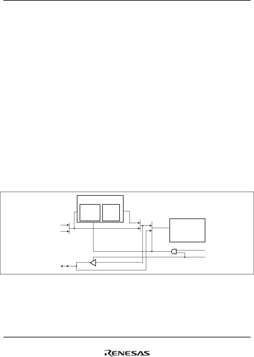
22. Serial I/O with FIFO (SIOF)
Rev.1.00 Jan. 10, 2008 Page 1128 of 1658
REJ09B0261-0100
22.4 Operation
22.4.1 Serial Clocks
(1) Master/Slave Modes
The following two modes are available as the SIOF clock mode.
• Slave mode: SIOF_SCK, SIOF_SYNC input
• Master mode: SIOF_SCK, SIOF_SYNC output
(2) Baud Rate Generator
In SIOF master mode, the baud rate generator (BRG) is used to generate the serial clock. The baud
rate generator consists of the prescaler that can select 32 types of division ratio from 1 to 1/32 with
the BRPS4 to BRSP0 bits in SISCR and divider that can select the division ratio from 1, 1/2, 1/4,
1/8, 1/16, and 1/32. The division ratio of the baud rate generator ranges from 1 to 1/1024 of the
product of the division ratios of the prescaler and the divider.
When the master clock is not divided by the baud rate generator (the division ratio is 1), set the
MSIMM bit in SISCR to 1 and use the master clock without division as a serial clock.
Figure 22.2 shows connections for supply of the serial clock.
Baud rate generator
Prescaler Divider
MCLK
1/1 to 1/1024 MCLK
Timing control
SCKE
Master
SIOF_SCK
SIOF_MCLK
Pck
Figure 22.2 Serial Clock Supply

22. Serial I/O with FIFO (SIOF)
Rev.1.00 Jan. 10, 2008 Page 1129 of 1658
REJ09B0261-0100
Table 22.5 shows an example of serial clock frequency.
Table 22.5 SIOF Serial Clock Frequency
Sampling Rate*
Frame Length 8 kHz 44.1 kHz 48 kHz
32 bits 256 kHz 1.4112 MHz 1.536 MHz
64 bits 512 kHz 2.8224 MHz 3.072 MHz
128 bits 1.024 MHz 5.6448 MHz 6.144 MHz
256 bits 2.048 MHz 11.289 MHz 12.289 MHz
Note: * Control data formats are valid when the FL bits are set to 1xxx (x: Don't care).
22.4.2 Serial Timing
(1) SIOF_SYNC
The SIOF_SYNC is a frame synchronous signal. Depending on the transfer mode, it has the
following two functions.
• Synchronous pulse: 1-bit-width pulse indicating the start of the frame
• L/R: 1/2-frame-width pulse indicating the left-channel stereo data (L) in high level and the
right-channel stereo data (R) in low level
Figure 22.3 shows the SIOF_SYNC synchronization timing.
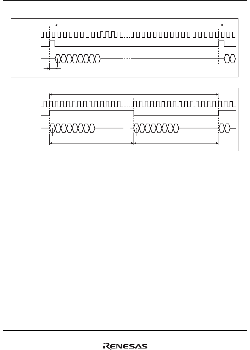
22. Serial I/O with FIFO (SIOF)
Rev.1.00 Jan. 10, 2008 Page 1130 of 1658
REJ09B0261-0100
SIOF_SCK
SIOF_RXD
SIOF_TXD
SIOF_SYNC
1-bit delay
Start bit data
1 frame
SIOF_SCK
SIOF_RXD
SIOF_TXD
SIOF_SYNC
Lch. Start bit of left channel data
(1/2 frame length)
1 frame
No delay
Rch. Start bit of right channel data
(1/2 frame length)
(b) L/R
(a) Synchronous pulse
Figure 22.3 Serial Data Synchronization Timing
(2) Transmit/Receive Timing
The SIOF_TXD transmit timing and SIOF_RXD receive timing relative to the SIOF_SCK can be
set as the sampling timing in the following two ways. The transmit/receive timing is set by the
REDG bit in SIMDR.
• Falling-edge sampling
• Rising-edge sampling
Figure 22.4 shows the transmit/receive timing.
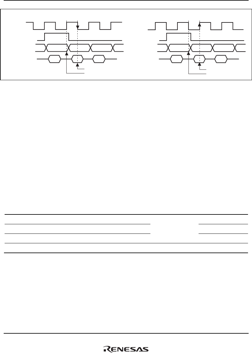
22. Serial I/O with FIFO (SIOF)
Rev.1.00 Jan. 10, 2008 Page 1131 of 1658
REJ09B0261-0100
SIOF_SCK
SIOF_SYNC
SIOF_TXD
SIOF_RXD
(a) Falling-edge sampling (REDG = 0)
SIOF_SCK
SIOF_SYNC
SIOF_TXD
SIOF_RXD
(b) Rising-edge sampling (REDG = 1)
Receive timing
Transmit timing
Receive timing
Transmit timing
Figure 22.4 SIOF Transmit/Receive Timing
22.4.3 Transfer Data Format
The SIOF performs the following transfer.
• Transmit/receive data: Transfer of 8-bit data/16-bit data/16-bit stereo data
• Control data: Transfer of 16-bit data (uses the transmit/receive control register as interface)
(1) Transfer Mode
As shown in table 22.6, the SIOF supports the following four transfer modes. The transfer mode
can be specified by the TRMD1 and TRMD0 bits in SIMDR.
Table 22.6 Serial Transfer Modes
TRMD1 and
TRMD0 Transfer Mode SIOF_SYNC Bit Delay Control Data*
00 Slave mode 1 Synchronous pulse Slot position
01 Slave mode 2 Synchronous pulse Secondary FS
10 Master mode 1 Synchronous pulse
SYNCDL bit
Slot position
11 Master mode 2 L/R No Not supported
Note: * The control data method is valid when the FL bits are set to B'1xxx (x: don't care).

22. Serial I/O with FIFO (SIOF)
Rev.1.00 Jan. 10, 2008 Page 1132 of 1658
REJ09B0261-0100
(2) Frame Length
The frame length to be transferred by the SIOF is specified by the FL3 to FL0 bits in SIMDR.
Table 22.7 shows the relationship between the setting values and frame length.
Table 22.7 Frame Length
FL3 to FL0 Slot Length
Number of Bits
in a Frame Transfer Data
00xx 8 8 8-bit monaural data
0100 8 16 8-bit monaural data
0101 8 32 8-bit monaural data
0110 8 64 8-bit monaural data
0111 8 128 8-bit monaural data
10xx 16 16 16-bit monaural data
1100 16 32 16-bit monaural/stereo data
1101 16 64 16-bit monaural/stereo data
1110 16 128 16-bit monaural/stereo data
1111 16 256 16-bit monaural/stereo data
Note: x: Don't care.
(3) Slot Position
The SIOF can specify the position of transmit data, receive data, and control data in a frame
(common to transmission and reception) by slot numbers. The slot number of each data is
specified by the following registers.
• Transmit data: SITDAR
• Receive data: SIRDAR
• Control data: SICDAR
Only 16-bit data is valid for control data. In addition, control data is always assigned to the same
slot number both in transmission and reception.
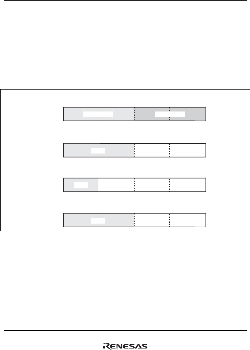
22. Serial I/O with FIFO (SIOF)
Rev.1.00 Jan. 10, 2008 Page 1133 of 1658
REJ09B0261-0100
22.4.4 Register Allocation of Transfer Data
(1) Transmit/Receive Data
Writing and reading of transmit/receive data is performed for the following registers.
• Transmit data writing: SITDR (32-bit access)
• Receive data reading: SIRDR (32-bit access)
Figure 22.5 shows the transmit/receive data and the SITDR and SIRDR bit alignment.
(a) 16-bit stereo data
(b) 16-bit monaural data
(c) 8-bit monaural data
(d) 16-bit stereo data (left and right same audio output)
31 24 23 16 15 8 7 0
31 24 23 16 15 8 7 0
31 24 23 16 15 8 7 0
31 24 23 16 15 8 7 0
L-channel data
Data
Data
Data
R-channel data
Figure 22.5 Transmit/Receive Data Bit Alignment
Note: In the figure, only the shaded areas are transmitted or received as valid data. Therefore,
access must be made in byte units for 8-bit data, and in word units for 16-bit data. Data in
not shaded areas is not transmitted or received.
Monaural or stereo can be specified for transmit data by the TDLE bit and TDRE bit in SITDAR.
Monaural or stereo can be specified for receive data by the RDLE bit and RDRE bit in SIRDAR.
To achieve left and right same audio output while stereo is specified for transmit data, set the
TLREP bit in SITDAR. Tables 22.8 and 22.9 show the audio mode specification for transmit data
and that for receive data, respectively.
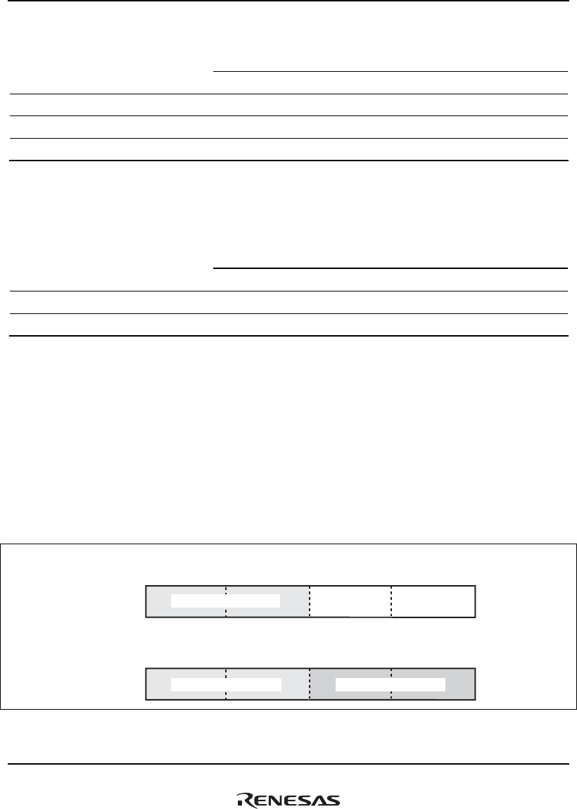
22. Serial I/O with FIFO (SIOF)
Rev.1.00 Jan. 10, 2008 Page 1134 of 1658
REJ09B0261-0100
Table 22.8 Audio Mode Specification for Transmit Data
Bit
Mode TDLE TDRE TLREP
Monaural 1 0 x
Stereo 1 1 0
Left and right same audio output 1 1 1
Legend:
x: Don't care
Table 22.9 Audio Mode Specification for Receive Data
Bit
Mode RDLE RDRE
Monaural 1 0
Stereo 1 1
Note: Left and right same audio mode is not supported in receive data.
To execute 8-bit monaural transmission or reception, use the left channel.
(2) Control Data
Control data is written to or read from by the following registers.
• Transmit control data write: SITCR (32-bit access)
• Receive control data read: SIRCR (32-bit access)
Figure 22.6 shows the control data and bit alignment in SITCR and SIRCR.
(b) Control data: Two channels
(a) Control data: One channel
31 24 23 16 15 8 7 0
31 24 23 16 15 8 7 0
Control data (channel 0)
Control data (channel 0) Control data (channel 1)
Figure 22.6 Control Data Bit Alignment
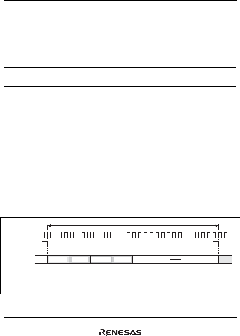
22. Serial I/O with FIFO (SIOF)
Rev.1.00 Jan. 10, 2008 Page 1135 of 1658
REJ09B0261-0100
The number of channels in control data is specified by the CD0E and CD1E bits in SICDAR.
Table 22.10 shows the relationship between the number of channels in control data and bit
settings.
Table 22.10 Number of Channels in Control Data
Bit
Number of Channels CD0E CD1E
1 1 0
2 1 1
Note: To use only one channel in control data, use channel 0.
22.4.5 Control Data Interface
Control data performs control command output to the CODEC and status input from the CODEC.
The SIOF supports the following two control data interface methods.
• Control by slot position
• Control by secondary FS
Control data is valid when data length is specified as 16 bits.
(1) Control by Slot Position (Master Mode 1 and Slave Mode 1)
Control data is transferred for all frames transmitted or received by the SIOF by specifying the slot
position of control data. This method can be used in both SIOF master and slave modes. Figure
22.7 shows an example of the control data interface timing by slot position control.
SIOF_SCK
SIOF_RXD
SIOF_TXD
SIOF_SYNC
1 frame
L-channel
data R-channel
data
Control
channel 0 Control
channel 0
Slot No.0 Slot No.1 Slot No.2 Slot No.3
TRMD[1:0] = 00 or 10,Specifications:
TDLE = 1,
RDLE = 1,
CD0E = 1,
REDG = 0
TDLA[3:0] = 0000,
RDLA[3:0] = 0000,
CD0A[3:0] = 0001,
FL[3:0] = 1110 (Frame length: 128 bits),
TDRE = 1,
RDRE = 1,
CD1E = 1,
TDRA[3:0] = 0010,
RDRA[3:0] = 0010,
CD1A[3:0] = 0011
Figure 22.7 Control Data Interface (Slot Position)
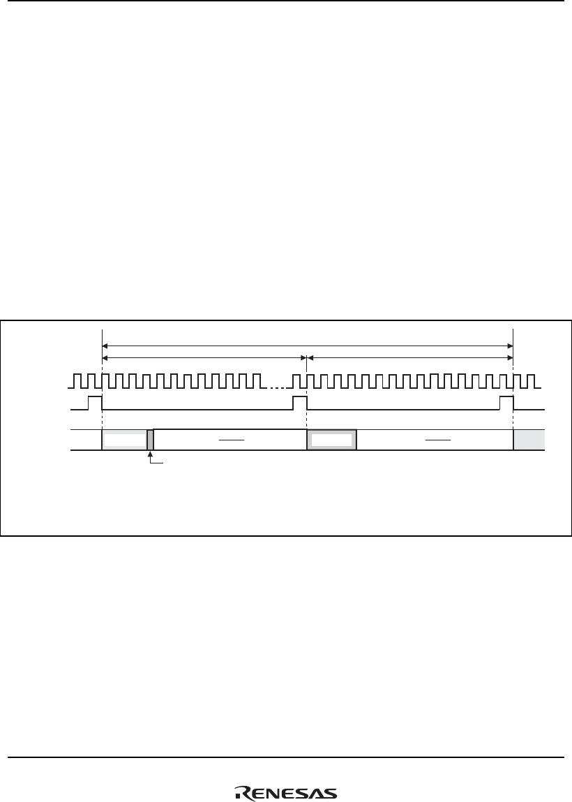
22. Serial I/O with FIFO (SIOF)
Rev.1.00 Jan. 10, 2008 Page 1136 of 1658
REJ09B0261-0100
(2) Control by Secondary FS (Slave Mode 2)
The CODEC normally outputs the SIOF_SYNC signal as synchronization pulse (FS). In this
method, the CODEC outputs the secondary FS specific to the control data transfer after 1/2 frame
time has been passed (not the normal FS output timing) to transmit or receive control data. This
method is valid for SIOF slave mode. The following summarizes the control data interface
procedure by the secondary FS.
• Transmit normal transmit data of LSB = 0 (the SIOF forcibly clears to 0).
• To execute control data transmission, send transmit data of LSB = 1 (the SIOF forcibly set to 1
by writing SITCDR).
• The CODEC outputs the secondary FS.
• The SIOF transmits or receives (stores in SIRCDR) control data (data specified by SITCDR)
synchronously with the secondary FS.
Figure 22.8 shows an example of the control data interface timing by the secondary FS.
TRMD[1:0] = 01,Specifications:
TDLE = 1,
RDLE = 1,
CD0E = 1,
REDG = 0
TDLA[3:0] = 0000,
RDLA[3:0] = 0000,
CD0A[3:0] = 0000,
FL[3:0] = 1110 (Frame length: 128 bits),
TDRE = 0,
RDRE = 0,
CD1E = 0,
TDRA[3:0] = 0000,
RDRA[3:0] = 0000,
CD1A[3:0] = 0000,
SIOF_SCK
SIOF_RXD
SIOF_TXD
SIOF_SYNC
1 frame
L-channel
data Control
channel 0
Slot No.0 Slot No.0
1/2 frame 1/2 frame
Secondary FS Normal FS
Normal FS
LSB = 1 (Secondary FS request)
Figure 22.8 Control Data Interface (Secondary FS)

22. Serial I/O with FIFO (SIOF)
Rev.1.00 Jan. 10, 2008 Page 1137 of 1658
REJ09B0261-0100
22.4.6 FIFO
(1) Overview
The transmit and receive FIFO systems of the SIOF have the following features.
• 16-stage 32-bit FIFOs for transmission and reception
• The FIFO pointer can be updated in one read or write cycle regardless of access size of the
CPU and DMAC. (One-stage 32-bit FIFO access cannot be divided into multiple accesses.)
(2) Transfer Request
The transfer request of the FIFO can be issued to the CPU or DMAC as the following interrupt
sources.
• FIFO transmit request: TDREQ (transmit interrupt source)
• FIFO receive request: RDREQ (receive interrupt source)
The request conditions for FIFO transmit or receive can be specified individually. The request
conditions for the FIFO transmit and receive are specified by the TFWM2 to TFWM0 bits and the
bits RFWM2 to RFWM0 in SIFCTR, respectively. Tables 22.11 and 22.12 summarize the
conditions to issue transmit request and those to issue receive request, respectively.
Table 22.11 Conditions to Issue Transmit Request
TFWM2 to
TFWM0
Number of
Requested Stages*1 Transmit Request Used Areas
000 1 Empty area is 16 stages
100 4 Empty area is 12 stages or more
101 8 Empty area is 8 stages or more
110 12 Empty area is 4 stages or more
Smallest
111*2 16 Empty area is 1 stage or more Largest
Notes: 1. The number of requested stages is the number of stages in transmit/receive FIFO.
2. Setting prohibited in DMA use.

22. Serial I/O with FIFO (SIOF)
Rev.1.00 Jan. 10, 2008 Page 1138 of 1658
REJ09B0261-0100
Table 22.12 Conditions to Issue Receive Request
RFWM2 to
RFWM0
Number of
Requested Stages* Receive Request Used Areas
000 1 Valid data is 1 stage or more
100 4 Valid data is 4 stages or more
101 8 Valid data is 8 stages or more
110 12 Valid data is 12 stages or more
Smallest
111 16 Valid data is 16 stages Largest
Note: * The number of requested stages is the number of stages in transmit/receive FIFO.
The number of stages of the FIFO is always sixteen even if the data area or empty area exceeds the
FIFO size. Accordingly, an overflow error or underflow error occurs if data area or empty area
exceeds sixteen FIFO stages.
The FIFO transmit or receive request is canceled when the above condition is not satisfied even if
the FIFO is not empty or full.
(3) Number of FIFOs
The number of FIFO stages used in transmission and reception is indicated by the following
register.
• Transmit FIFO: The number of empty FIFO stages is indicated by the TFUA4 to TFUA0 bits
in SIFCTR.
• Receive FIFO: The number of valid data stages is indicated by the bits RFUA4 to RFUA0 bits
in SIFCTR.
The above indicates possible data numbers that can be transferred by the CPU or DMAC.
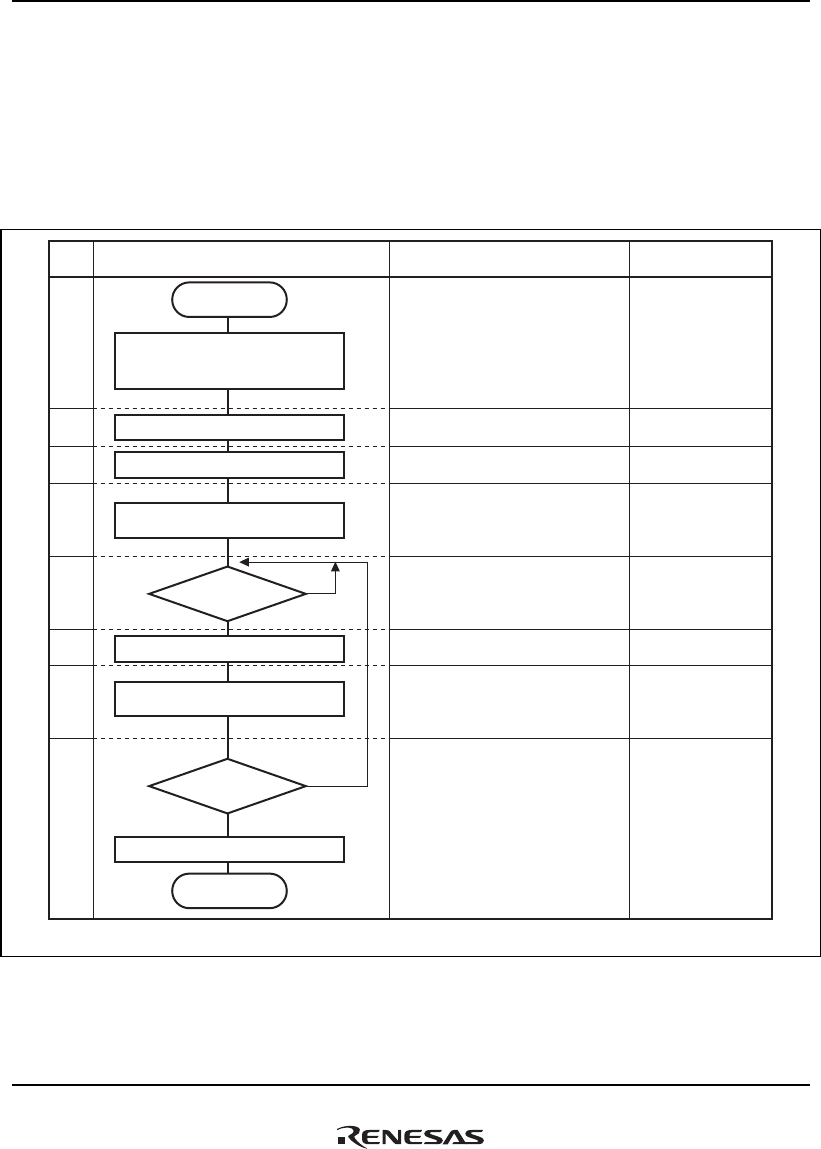
22. Serial I/O with FIFO (SIOF)
Rev.1.00 Jan. 10, 2008 Page 1139 of 1658
REJ09B0261-0100
22.4.7 Transmit and Receive Procedures
Set each register after setting the PFC.
(1) Transmission in Master Mode
Figure 22.9 shows an example of settings and operation for master mode transmission.
Start
End
Set the SCKE bit in SICTR to 1
Start SIOF_SCK output
Set SITDR
Set the TXE bit in SICTR to 0
Transmit SITDR from SIOF_TXD
synchronously with SIOF_SYNC
TDREQ = 1
Transfer ended?
No
Yes
No
Yes
No.
1
2
3
4
5
6
7
8
Flowchart SIOF Settings SIOF Operation
Set operation start for baud rate generator
Output serial clock
Set transmit data
Set to disable transmission End transmission
Set the start for frame synchronous signal
output and enable transmission
Output frame
synchronous signal and
issue transmit transfer
request*
Transmit
Note: * When interrupts due to transmit data underflow are enabled, after setting the no. 6 transmit data, the TXE bit should be set to 1.
Set SIMDR, SISCR, SITDAR,
SIRDAR, SICDAR, SITCR,
and SIFCTR
Set the FSE and TXE bits in SICTR to 1
Set operating mode, serial clock, slot
positions for transmit/receive data, slot
position for control data, and FIFO
request threshold value
Figure 22.9 Example of Transmit Operation in Master Mode
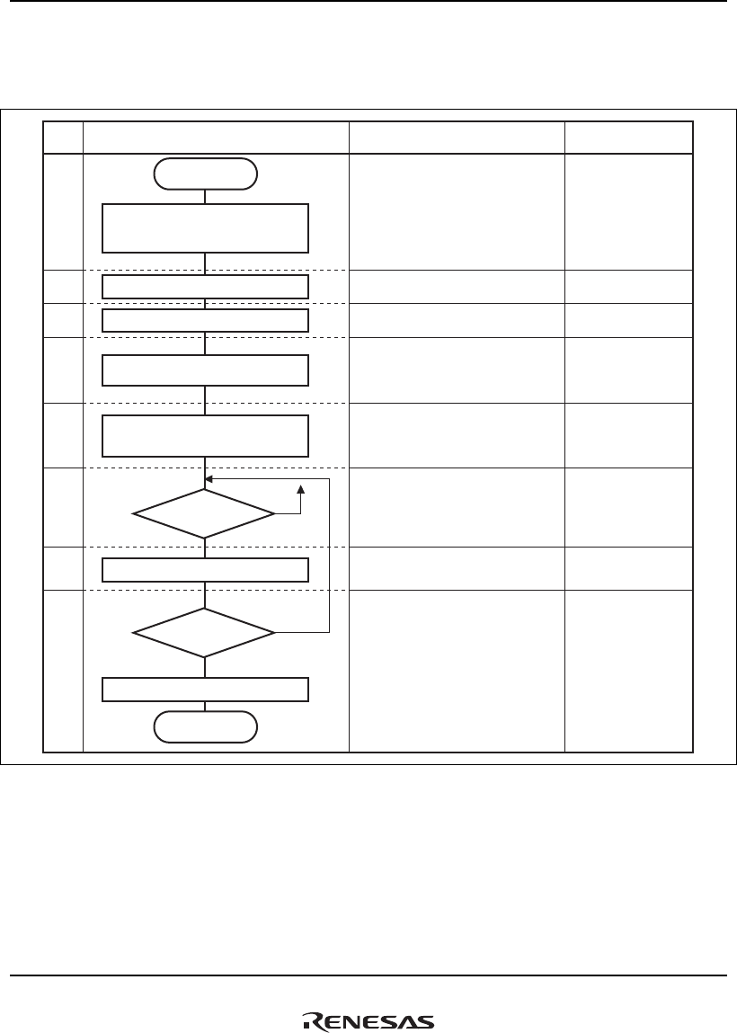
22. Serial I/O with FIFO (SIOF)
Rev.1.00 Jan. 10, 2008 Page 1140 of 1658
REJ09B0261-0100
(2) Reception in Master Mode
Figure 22.10 shows an example of settings and operation for master mode reception.
Start
End
Set the SCKE bit in SICTR to 1
Start SIOF_SCK output
Read SIRDR
Clear the RXE bit in SICTR to 0
RDREQ = 1
Transfer ended?
No
Yes
No
Yes
No.
1
2
3
4
5
6
7
8
Flowchart SIOF Settings SIOF Operation
Set operation start for baud rate generator
Output serial clock
Read receive data
Receive
Set to disable reception End reception
Set the start for frame synchronous signal
output and enable reception
Output frame
synchronous signal
Issue receive transfer
request according to
the receive FIFO
threshold value
Set SIMDR, SISCR, SITDAR,
SIRDAR, SICDAR, SITCR,
and SIFCTR
Set the FSE and RXE bits in SICTR to 1
Store SIOF_RXD receive data in SIRDR
synchronously with SIOF_SYNC
Set operating mode, serial clock, slot
positions for transmit/receive data, slot
position for control data, and FIFO
request threshold value
Figure 22.10 Example of Receive Operation in Master Mode
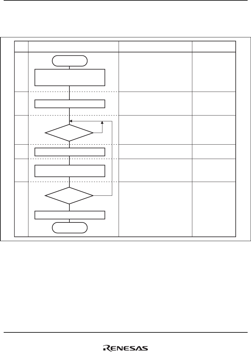
22. Serial I/O with FIFO (SIOF)
Rev.1.00 Jan. 10, 2008 Page 1141 of 1658
REJ09B0261-0100
(3) Transmission in Slave Mode
Figure 22.11 shows an example of settings and operation for slave mode transmission.
Start
End
Set the TXE bit in SICTR to 1
Set SITDR
Clear the TXE bit in SICTR to 0
TDREQ = 1
Transfer ended?
No
Yes
No
Yes
No.
1
2
3
4
6
Flowchart SIOF Settings SIOF Operation
Set to enable transmission
Issue transmit transfer
request to enable
transmission when frame
synchronous signal is
input
Set transmit data
Transmit SITDR from SIOF_TXD
synchronously with SIOF_SYNC
5Transmit
Set to disable transmission End transmission
Set SIMDR, SISCR, SITDAR,
SIRDAR, SICDAR, SITCR,
and SIFCTR
Set operating mode, serial clock, slot
positions for transmit/receive data, slot
position for control data, and FIFO
request threshold value
Figure 22.11 Example of Transmit Operation in Slave Mode
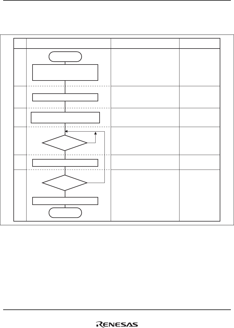
22. Serial I/O with FIFO (SIOF)
Rev.1.00 Jan. 10, 2008 Page 1142 of 1658
REJ09B0261-0100
(4) Reception in Slave Mode
Figure 22.12 shows an example of settings and operation for slave mode reception.
Start
End
Set the RXE bit in SICTR to 1
Read SIRDR
Clear the RXE bit in SICTR to 0
RDREQ = 1
Transfer ended?
No
Yes
No
Yes
No.
1
2
3
4
6
Flowchart SIOF Settings SIOF Operation
Set to enable reception
Enable reception when
the frame synchronous
signal is input
Read receive data
Store SIOF_RXD receive data in SIRDR
synchronously with SIOF_SYNC
5
Issue receive transfer
request according to the
receive FIFO threshold
value
Set to disable reception End reception
Receive
Set SIMDR, SISCR, SITDAR,
SIRDAR, SICDAR, SITCR,
and SIFCTR
Set operating mode, serial clock, slot
positions for transmit/receive data, slot
position for control data, and FIFO
request threshold value
Figure 22.12 Example of Receive Operation in Slave Mode

22. Serial I/O with FIFO (SIOF)
Rev.1.00 Jan. 10, 2008 Page 1143 of 1658
REJ09B0261-0100
(5) Transmit/Receive Reset
The SIOF can separately reset the transmit and receive units by setting the following bits to 1.
• Transmit reset: TXRST bit in SICTR
• Receive reset: RXRST bit in SICTR
Table 22.13 shows the details on initialization upon transmit or receive reset.
Table 22.13 Transmit and Receive Reset
Type Objects to be Initialized
Transmit reset Stop transmitting from SIOF_TXD (output according to the value set in
the TXDIZ bit)
Transmit FIFO write pointer
TCRDY, TFEMP, and TDREQ bits in SISTR
TXE bit in SICTR
Receive reset Stop receiving from SIOF_RXD
Receive FIFO read pointer
RCRDY, RFFUL, and RDREQ bits in SISTR
RXE bit in SICTR

22. Serial I/O with FIFO (SIOF)
Rev.1.00 Jan. 10, 2008 Page 1144 of 1658
REJ09B0261-0100
22.4.8 Interrupts
The SIOF has one type of interrupt.
(1) Interrupt Sources
Interrupts can be issued by several sources. Each source is shown as an SIOF status in SISTR.
Table 22.14 lists the SIOF interrupt sources.
Table 22.14 SIOF Interrupt Sources
No. Classification Bit Name Function Name Description
1 TDREQ Transmit FIFO transfer
request
The transmit FIFO stores data of
specified size or more.
2
Transmission
TFEMP Transmit FIFO empty The transmit FIFO is empty.
3 RDREQ Receive FIFO transfer
request
The receive FIFO stores data of
specified size or more.
4
Reception
RFFUL Receive FIFO full The receive FIFO is full.
5 TCRDY Transmit control data
ready
The transmit control register is ready to
be written to.
6
Control
RCRDY Receive control data
ready
The receive control data register stores
valid data.
7 Error TFUDF Transmit FIFO
underflow
Serial data transmit timing has arrived
while the transmit FIFO is empty.
8 TFOVF Transmit FIFO overflow Write to the transmit FIFO is performed
while the transmit FIFO is full.
9 RFOVF Receive FIFO overflow Serial data is received while the receive
FIFO is full.
10 RFUDF Receive FIFO
underflow
The receive FIFO is read while the
receive FIFO is empty.
11 FSERR Frame Synchronous
Error
A synchronous signal is input before
the specified bit number has been
passed (in slave mode).
12 SAERR Slot assign error The same slot is specified in both serial
data and control data.
Whether an interrupt is issued or not as the result of an interrupt source is determined by the
SIIER settings. If an interrupt source is set to 1 and the corresponding bit in SIIER is set to 1, an
SIOF interrupt is issued.

22. Serial I/O with FIFO (SIOF)
Rev.1.00 Jan. 10, 2008 Page 1145 of 1658
REJ09B0261-0100
(2) Regarding Transmit and Receive Classification
The transmit sources and receive sources are signals indicating the state; after being set, if the state
changes, they are automatically cleared by the SIOF.
When the DMA transfer is used, a DMA transfer request is pulled low for one cycle at the end of
DMA transfer.
(3) Processing when Errors Occur
On occurrence of each of the errors indicated as a status in SISTR, the SIOF performs the
following operations.
• Transmit FIFO underflow (TFUDF)
The immediately preceding transmit data is again transmitted.
• Transmit FIFO overflow (TFOVF)
The contents of the transmit FIFO are protected, and the write operation causing the overflow
is ignored.
• Receive FIFO overflow (RFOVF)
Data causing the overflow is discarded and lost.
• Receive FIFO underflow (RFUDF)
An undefined value is output on the bus.
• Frame synchronization error (FSERR)
The internal counter is reset according to the signal in which an error occurs.
• Slot assign error (SAERR)
⎯ If the same slot is assigned to both serial data and control data, the slot is assigned to serial
data.
⎯ If the same slot is assigned to two control data items, the data cannot be transferred
correctly.
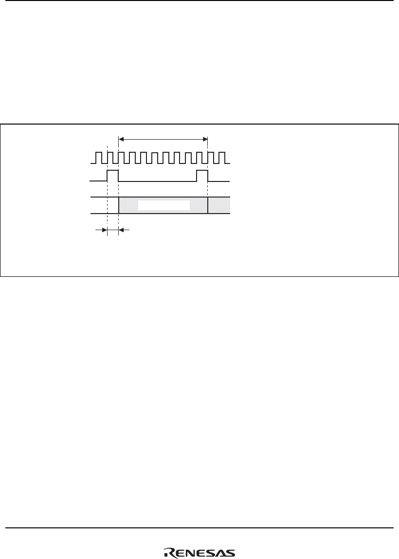
22. Serial I/O with FIFO (SIOF)
Rev.1.00 Jan. 10, 2008 Page 1146 of 1658
REJ09B0261-0100
22.4.9 Transmit and Receive Timing
Figures 22.13 to 22.19 show examples of the SIOF serial transmission and reception.
(1) 8-bit Monaural Data (1)
Synchronous pulse method, falling edge sampling, slot No.0 used for transmit and receive data, a
frame length = 8 bits
Slot No.0
TRMD[1:0] = 00 or 10,
TDLE = 1,
RDLE = 1,
CD0E = 0,
REDG = 0,
TDLA[3:0] = 0000,
RDLA[3:0] = 0000,
CD0A[3:0] = 0000,
FL[3:0] = 0000 (frame length: 8 bits)
TDRE = 0,
RDRE = 0,
CD1E = 0,
TDRA[3:0] = 0000,
RDRA[3:0] = 0000,
CD1A[3:0] = 0000
Specifications:
1 frame
1-bit delay
SIOF_SCK
SIOF_RXD
SIOF_TXD
SIOF_SYNC
SYNCDL = 1
L-channel data
Figure 22.13 Transmit and Receive Timing (8-Bit Monaural Data (1))

22. Serial I/O with FIFO (SIOF)
Rev.1.00 Jan. 10, 2008 Page 1147 of 1658
REJ09B0261-0100
(2) 8-bit Monaural Data (2)
Synchronous pulse method, falling edge sampling, slot No.0 used for transmit and receive data,
and frame length = 16 bits
TRMD[1:0] = 00 or 10,
TDLE = 1,
RDLE = 1,
CD0E = 0,
REDG = 0,
TDLA[3:0] = 0000,
RDLA[3:0] = 0000,
CD0A[3:0] = 0000,
FL[3:0] = 0100 (frame length: 16 bits)
TDRE = 0,
RDRE = 0,
CD1E = 0,
TDRA[3:0] = 0000,
RDRA[3:0] = 0000,
CD1A[3:0] = 0000
Slot No.0 Slot No.1
Specifications:
1 frame
1-bit delay
SIOF_SCK
SIOF_RXD
SIOF_TXD
SIOF_SYNC
SYNCDL = 1
L-channel data
Figure 22.14 Transmit and Receive Timing (8-Bit Monaural Data (2))
(3) 16-bit Monaural Data
Synchronous pulse method, falling edge sampling, slot No.0 used for transmit and receive data,
and frame length = 64 bits
TRMD[1:0] = 00 or 10,
TDLE = 1,
RDLE = 1,
CD0E = 0,
REDG = 0,
TDLA[3:0] = 0000,
RDLA[3:0] = 0000,
CD0A[3:0] = 0000,
FL[3:0] = 1101 (frame length: 64 bits)
TDRE = 0,
RDRE = 0,
CD1E = 0,
TDRA[3:0] = 0000,
RDRA[3:0] = 0000,
CD1A[3:0] = 0000
Slot No.0 Slot No.1 Slot No.2 Slot No.3
Specifications:
1 frame
1-bit delay
SYNCDL = 1
SIOF_SCK
SIOF_RXD
SIOF_TXD
SIOF_SYNC
L-channel data
Figure 22.15 Transmit and Receive Timing (16-Bit Monaural Data)
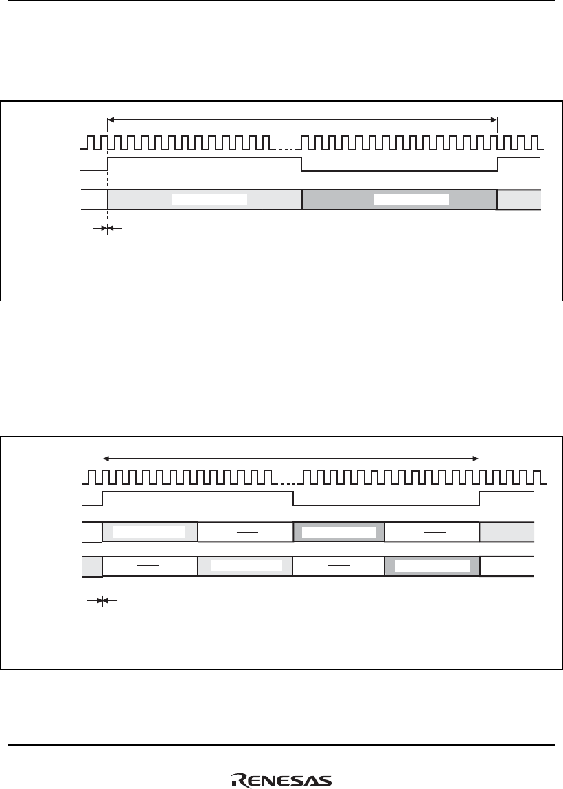
22. Serial I/O with FIFO (SIOF)
Rev.1.00 Jan. 10, 2008 Page 1148 of 1658
REJ09B0261-0100
(4) 16-bit Stereo Data (1)
L/R method, rising edge sampling, slot No.0 used for left-channel data, slot No.1 used for right-
channel data, and frame length = 32 bits
TRMD[1:0] = 11,
TDLE = 1,
RDLE = 1,
CD0E = 0,
REDG = 1,
TDLA[3:0] = 0000,
RDLA[3:0] = 0000,
CD0A[3:0] = 0000,
FL[3:0] = 1101 (frame length: 32 bits)
TDRE = 1,
RDRE = 1,
CD1E = 0,
TDRA[3:0] = 0001,
RDRA[3:0] = 0001,
CD1A[3:0] = 0000
Slot No.0 Slot No.1
Specifications:
1 frame
No bit delay
SIOF_SCK
SIOF_RXD
SIOF_TXD
SIOF_SYNC
L-channel data R-channel data
Figure 22.16 Transmit and Receive Timing (16-Bit Stereo Data (1))
(5) 16-bit Stereo Data (2)
L/R method, rising edge sampling, slot No.0 used for left-channel transmit data, slot No.1 used for
left-channel receive data, slot No.2 used for right-channel transmit data, slot No.3 used for right-
channel receive data, and frame length = 64 bits
TRMD[1:0] = 11,
TDLE = 1,
RDLE = 1,
CD0E = 0,
REDG = 1,
TDLA[3:0] = 0000,
RDLA[3:0] = 0001,
CD0A[3:0] = 0000,
FL[3:0] = 1101 (frame length: 64 bits),
TDRE = 1,
RDRE = 1,
CD1E = 0,
TDRA[3:0] = 0010,
RDRA[3:0] = 0011,
CD1A[3:0] = 0000
Slot No.0 Slot No.1 Slot No.2 Slot No.3
Specifications:
1 frame
No bit delay
SIOF_SCK
SIOF_RXD
SIOF_TXD
SIOF_SYNC
R-channel data
L-channel data
L-channel data R-channel data
Figure 22.17 Transmit and Receive Timing (16-Bit Stereo Data (2))
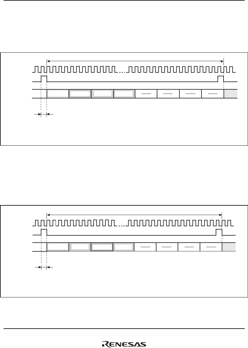
22. Serial I/O with FIFO (SIOF)
Rev.1.00 Jan. 10, 2008 Page 1149 of 1658
REJ09B0261-0100
(6) 16-bit Stereo Data (3)
Synchronous pulse method, falling edge sampling, slot No.0 used for left-channel data, slot No.1
used for right-channel data, slot No.2 used for control channel 0 data, slot No.3 used for control
channel 1 data, and frame length = 128 bits
TRMD[1:0] = 00 or 10,
TDLE = 1,
RDLE = 1,
CD0E = 1,
REDG = 0,
TDLA[3:0] = 0000,
RDLA[3:0] = 0000,
CD0A[3:0] = 0010,
FL[3:0] = 1110 (frame length: 128 bits),
TDRE = 1,
RDRE = 1,
CD1E = 1,
TDRA[3:0] = 0001,
RDRA[3:0] = 0001,
CD1A[3:0] = 0011
Slot No.0 Slot No.1 Slot No.2 Slot No.3 Slot No.4 Slot No.5 Slot No.6 Slot No.7
Specifications:
1 frame
1 bit delay
SYNCDL = 1
SIOF
_
SCK
SIOF
_
RXD
SIOF
_
TXD
SIOF
_
SYNC
L-channel
data R-channel
data Control
channel 0 Control
channel 1
Figure 22.18 Transmit and Receive Timing (16-Bit Stereo Data (3))
(7) 16-bit Stereo Data (4)
Synchronous pulse method, falling edge sampling, slot No.0 used for left-channel data, slot No.2
used for right-channel data, slot No.1 used for control channel 0 data, slot No.3 used for control
channel 1 data, and frame length = 128 bits
TRMD[1:0] = 00 or 10,
TDLE = 1,
RDLE = 1,
CD0E = 1,
REDG = 1,
TDLA[3:0] = 0000,
RDLA[3:0] = 0000,
CD0A[3:0] = 0001,
FL[3:0] = 1110 (frame length: 128 bits)
TDRE = 1,
RDRE = 1,
CD1E = 1,
TDRA[3:0] = 0010,
RDRA[3:0] = 0010,
CD1A[3:0] = 0011
Slot No.0 Slot No.1 Slot No.2 Slot No.3 Slot No.4 Slot No.5 Slot No.6 Slot No.7
Specifications:
1 frame
1 bit delay
SYNCDL = 1
SIOF_SCK
SIOF_RXD
SIOF_TXD
SIOF_SYNC
L-channel
data Control
channel 0 Control
channel 1
R-channel
data
Figure 22.19 Transmit and Receive Timing (16-Bit Stereo Data (4))
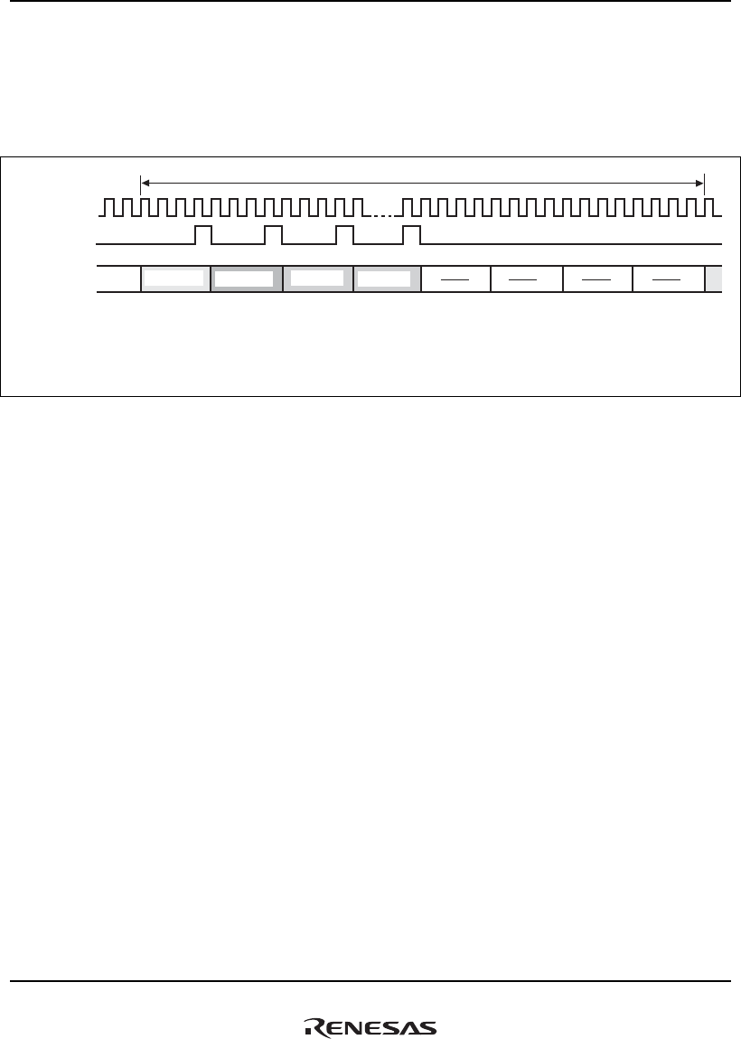
22. Serial I/O with FIFO (SIOF)
Rev.1.00 Jan. 10, 2008 Page 1150 of 1658
REJ09B0261-0100
(8) Synchronization-Pulse Output Mode at End of Each Slot (SYNCAT Bit = 1)
Synchronous pulse method, falling edge sampling, slot No.0 used for left-channel data, slot No.1
used for right-channel data, slot No.2 used for control channel 0 data, slot No.3 used for control
channel 1 data, and frame length = 128 bits
TRMD[1:0] = 00 or 10,
TDLE = 1,
RDLE = 1,
CD0E = 1,
REDG = 0,
TDLA[3:0] = 0000,
RDLA[3:0] = 0000,
CD0A[3:0] = 0010,
FL[3:0] = 1110 (frame length: 128 bits),
TDRE = 1,
RDRE = 1,
CD1E = 1,
TDRA[3:0] = 0001,
RDRA[3:0] = 0001,
CD1A[3:0] = 0011
Slot No.0 Slot No.1 Slot No.2 Slot No.3 Slot No.4 Slot No.5 Slot No.6 Slot No.7
Specifications:
1 frame
SIOF
_
SCK
SIOF
_
RXD
SIOF
_
TXD
SIOF
_
SYNC
L-channel
data R-channel
data Control
channel 0 Control
channel 1
Figure 22.20 Transmit and Receive Timing (16-Bit Stereo Data)

23. Serial Peripheral Interface (HSPI)
Rev.1.00 Jan. 10, 2008 Page 1151 of 1658
REJ09B0261-0100
Section 23 Serial Peripheral Interface (HSPI)
This LSI incorporates one channel of the Serial Protocol Interface (HSPI).
23.1 Features
The HSPI has the following features.
• Operating mode: Master mode or Slave mode.
• The transmit and receive sections within the module are double buffered to allow duplex
communication.
• A flexible peripheral clock (Pck) division strategy allows a wide range of bit rates to be
supported.
• The programmable clock control logic allows setting for two different transmit protocols and
accommodates transmit and receive functions on either edge of the serial clock.
• Error detection logic is provided for warning of the receive buffer overflow.
• The HSPI has a facility to generate the chip select signal to slave modules when configured as
a master either automatically as part of the data transfer process, or under the manual control
of the host processor.
• Both the transmit data and receive data can be DMA transferred independently via the two
DMA channels.
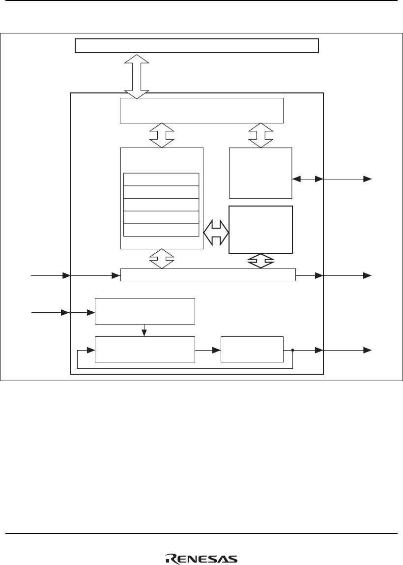
23. Serial Peripheral Interface (HSPI)
Rev.1.00 Jan. 10, 2008 Page 1152 of 1658
REJ09B0261-0100
Figure 23.1 is a block diagram of the HSPI.
HSPI_CLK
HSPI_TX
HSPI_RX LSB MSB
SPCR
HSPI_CS
SPSR
SPSCR
SPTBR
SPRBR
Pck
In FIFO mode
Peripheral bus
Transmit FIFO
Receive FIFO
(Eight entries
for each)
LSB MSB
Bus interface
Registers
System
control
Shift register
Clock division
Polarity selection SCK generator
Figure 23.1 Block Diagram of HSPI

23. Serial Peripheral Interface (HSPI)
Rev.1.00 Jan. 10, 2008 Page 1153 of 1658
REJ09B0261-0100
23.2 Input/Output Pins
The input/output pins of the HSPI is shown in table 23.1.
Table 23.1 Pin Configuration
Pin Name Abbrev. I/O Description
Serial bit clock pin HSPI_CLK I/O Clock input/output
Transmit data pin HSPI_TX Output Transmit data output
Receive data pin HSPI_RX Input Receive data input
Chip select pin HSPI_CS I/O Chip select
23.3 Register Descriptions
Table 23.2 Register Configuration (1)
Register Name Abbrev. R/W P4 Address Area 7 Address Size
Sync
Clock
Control register SPCR R/W H'FFE5 0000 H'1FE5 0000 32 Pck
Status register SPSR R* H'FFE5 0004 H'1FE5 0004 32 Pck
System control register SPSCR R/W H'FFE5 0008 H'1FE5 0008 32 Pck
Transmit buffer register SPTBR R/W H'FFE5 000C H'1FE5 000C 32 Pck
Receive buffer register SPRBR R H'FFE5 0010 H'1FE5 0010 32 Pck
Note: For bits 4 and 3, only 0s can be written to clear the flags.

23. Serial Peripheral Interface (HSPI)
Rev.1.00 Jan. 10, 2008 Page 1154 of 1658
REJ09B0261-0100
Table 23.3 Register Configuration (2)
Register Name Abbrev.
Power-on Reset
by PRESET
Pin/WDT/H-UDI
Manual Reset
by WDT/
Multiple
Exception
Sleep/Deep
Sleep by
SLEEP
Instruction
Module
Standby
Software
Reset
Control register SPCR H'0000 0000 H'0000 0000 Retained Retained Retained
Status register SPSR H'xxxx xx20*1 H'xxxx xx20*1 Retained Retained H'xxxx xxxx*2
System control register SPSCR H'0000 0040 H'0000 0040 Retained Retained Retained
Transmit buffer register SPTBR H'0000 0000 H'0000 0000 Retained Retained Retained
Receive buffer register SPRBR H'0000 0000 H'0000 0000 Retained Retained Retained
Notes: 1. "x" represents an undefined value.
2. "x" represents an undefined value. Bits 9, 6, 4, and 3 are retained. The other bits are
initialized except those of which the initial values are undefined.

23. Serial Peripheral Interface (HSPI)
Rev.1.00 Jan. 10, 2008 Page 1155 of 1658
REJ09B0261-0100
23.3.1 Control Register (SPCR)
SPCR is a 32-bit readable/writable register that controls the transfer data of shift timing and
specifies the clock polarity and frequency.
161718192021222324252627282931 30
————————————————
RRRRRRRRRRRRRRRR
Bit:
Initial value:
R/W:
01234567891011121315 14
00000000
CLKC0CLKC1CLKC2CLKC3CLKC4
IDIVCLKPFBS————————
0000000000000000
00000000
R/WR/WR/WR/WR/WR/WR/WR/WRRRRRRRR
Bit:
Initial value:
R/W:
Bit Bit Name
Initial
Value R/W Description
31 to 8 ⎯ All 0 R Reserved
These bits are always read as an undefined value. The
write value should always be 0.
7 FBS 0 R/W First Bit Start
Controls the timing relationship between each bit of
transferred data and the serial clock.
0: The first bit transmitted from the HSPI module is set
up such that it can be sampled by the receiving device at
the first edge of HSPI_CLK specified by the register after
the HSPI_CS pin goes low. Similarly the first received bit
is sampled at the first edge of HSPI_CLK after the
HSPI_CS pin goes low.
1: The first bit transmitted from the HSPI module is set
up such that it can be sampled by the receiving device at
the second edge of HSPI_CLK after the HSPI_CS pin
goes low. Similarly the first received bit is sampled at the
second edge of HSPI_CLK specified by the register after
the HSPI_CS pin goes low.
6 CLKP 0 R/W Serial Clock Polarity
0: HSPI_CLK signal is not inverted and so is low when
inactive.
1: HSPI_CLK signal is inverted and so is high when
inactive.

23. Serial Peripheral Interface (HSPI)
Rev.1.00 Jan. 10, 2008 Page 1156 of 1658
REJ09B0261-0100
Bit Bit Name
Initial
Value R/W Description
5 IDIV 0 R/W Initial Clock Division Ratio
0: The peripheral clock (Pck) is divided by a factor of 4
initially to create an intermediate frequency, which is
further divided to create the serial clock for master
mode.
1: The peripheral clock (Pck) is divided by a factor of 32
initially to create an intermediate frequency, which is
further divided to create the serial clock for master
mode.
4 to 0 CLKC4 to
CLKC0
All 0 R/W Clock Division Count
These bits determine the frequency dividing ratio that is
used to obtain the serial clock from the intermediate
clock.
00000: 1 intermediate frequency cycle.
Serial clock frequency = Intermediate
frequency / 2.
00001: 2 Intermediate frequency cycles.
Serial clock frequency = Intermediate
frequency / 4.
00010: 3 intermediate frequency cycles.
Serial clock frequency = Intermediate
frequency / 6.
: :
11111: 32 intermediate frequency cycles.
Serial clock frequency = Intermediate
frequency / 64.

23. Serial Peripheral Interface (HSPI)
Rev.1.00 Jan. 10, 2008 Page 1157 of 1658
REJ09B0261-0100
The serial clock frequency can be computed using the following formula:
Peripheral clock frequency
(Initial division ratio × (Clock division count + 1) × 2)
Serial clock frequency =
When the HSPI is configured as a slave, the IDIV and CLKC bits are ignored and the HSPI
synchronizes to the externally supplied serial clock. The maximum value of the external serial
clock that the module can operate with is Pck / 8.
If any of the FBS, CLKP, IDIV or CLKC bit values are changed, the HSPI will undergo a
software reset.
When IPIV or CLKC is specified or changed, the internal serial clock generation counter is reset.
In this case, data transmit/receive should be performed after the time length of at least one serial
clock cycle (depends on IDIV or CLKC specified) has elapsed.

23. Serial Peripheral Interface (HSPI)
Rev.1.00 Jan. 10, 2008 Page 1158 of 1658
REJ09B0261-0100
23.3.2 Status Register (SPSR)
SPSR is a 32-bit readable/writable register. Through the status flags in SPSR, it can be confirmed
whether or not the system is correctly operating. If the ROIE bit in SPSCR is set to 1, an interrupt
request is generated due to the occurrence of the receive buffer overrun error or the warning of the
receive buffer overrun error. When the TFIE bit in SPSCR is set to 1, an interrupt request is
generated by the transmit complete status flag. If the appropriate enable bit in SPSCR is set to 1,
an interrupt request is generated due to the receive FIFO halfway, receive FIFO full, transmit
FIFO empty, or transmit FIFO halfway flag. If the RNIE bit in SPSCR is set to 1, an interrupt
request is generated when the receive FIFO is not empty.
161718192021222324252627282931 30
————————————————
RRRRRRRRRRRRRRRR
Bit:
Initial value:
R/W:
01234567891011121315 14
00000100100
TXFLTXFNRXFLRXOWRXOO
RXEMRXHARXFUTXEMTXHATXFU—————
————————————————
—————
RRRR/W*R/W*RRRRRRRRRRR
Bit:
Initial value:
R/W:
Bit Bit Name
Initial
Value R/W Description
31 to 11 ⎯ Undefined R Reserved
These bits are always read as an undefined value. The
write value should always be 0.
10 TXFU 0 R Transmit FIFO Full Flag
This status flag is enabled only in FIFO mode. The flag
is set to 1 when the transmit FIFO is full of bytes for
transmission and cannot accept any more. It is cleared
to 0 when data is transmitted from the transmit FIFO to
the HSPI bus.
9 TXHA 0 R Transmit FIFO Halfway Flag
This status flag is enabled only in FIFO mode. The flag
is set to 1 when the transmit FIFO reaches the halfway
point, that is, it has four bytes of data and free space for
four bytes of data. It is cleared to 0 when more data is
written to the transmit FIFO. It remains set to 1 until
cleared to 0 even if data stored in the FIFO becomes
less than four bytes (halfway point).
If TXHA = 1 and THIE = 1, an interrupt is generated.

23. Serial Peripheral Interface (HSPI)
Rev.1.00 Jan. 10, 2008 Page 1159 of 1658
REJ09B0261-0100
Bit Bit Name
Initial
Value R/W Description
8 TXEM 1 R Transmit FIFO Empty Flag
This status flag is enabled only in FIFO mode. The flag
is set to 1 when the transmit FIFO is empty of data to
transmit. It is cleared to 0 when data is written to the
transmit FIFO.
If TXEM = 1 and TEIE = 1, an interrupt is generated.
7 RXFU 0 R Receive FIFO Full Flag
This status flag is enabled only in FIFO mode. The flag
is set to 1 when the receive FIFO is full of received
bytes and cannot accept any more. It is cleared to 0
when data is read out of the receive FIFO.
If RXFU = 1 and RFIE = 1, an interrupt is generated.
6 RXHA 0 R Receive FIFO Halfway Flag
This status flag is enabled only in FIFO mode. The flag
is set to 1 when the receive FIFO reaches the halfway
point, that is, it has four bytes of data and free space for
four bytes of data. This flag is cleared to 0 when the
receive data is read from receive FIFO and the data
stored in the FIFO becomes less than four bytes
(halfway point).
If RXHA = 1 and RHIE = 1, an interrupt is generated.
5 RXEM 1 R Receive FIFO Empty Flag
This status flag is enabled only in FIFO mode. The flag
is set to 1 when the receive FIFO is empty of received
data. It is cleared to 0 when data is written to the
receive FIFO.
If RXEM = 0 and RNIE = 1, an interrupt is generated.
4 RXOO 0 R/W* Receive Buffer Overrun Occurred Flag
This status flag is set to 1 when new data has been
received but the previous received data has not been
read from SPRBR. The previously received data will not
be overwritten by the newly received data. The RXOO
flag remains set to 1 until writing 0 to this bit position.
If RXOO = 1 and ROIE = 1, an interrupt is generated.

23. Serial Peripheral Interface (HSPI)
Rev.1.00 Jan. 10, 2008 Page 1160 of 1658
REJ09B0261-0100
Bit Bit Name
Initial
Value R/W Description
3 RXOW 0 R/W* Receive Buffer Overrun Warning Flag
This status flag is set to 1 when a new serial data
transfer has started before the previous received data is
read from SPRBR. The RXOW remains set to 1 until
writing 0 to this bit position.
If RXOW= 1 and ROIE = 1, an interrupt is generated.
2 RXFL 0 R Receive Buffer Full Status Flag
This status flag indicates that new data is available in
the SPRBR and has not yet been read. It is set to 1
when the shift register contents are loaded into the
SPRBR in the end of a serial bus transfer. This bit is
cleared to 0 by reading SPRBR.
1 TXFN 0 R Transmit Complete Status Flag
This status flag indicates that the last transmission has
been completed. It is set to 1 when SPTBR is ready to
accept data from the peripheral bus. This bit is cleared
to 0 by writing data to SPTBR.
If TXFN = 1 and TFIE = 1, an interrupt is generated.
0 TXFL 0 R Transmit Buffer Full Status Flag
This status flag indicates the SPTBR stores data that
has not been transmitted. It is set to 1 when SPTBR is
written with data from the peripheral bus. This bit is
cleared to 0 when SPTBR is ready to accept data from
the peripheral bus.
Note: * These bits are readable/writable bits. Writing 0 initializes these bits to the initial values
of respective bits, while writing 1 is ignored.

23. Serial Peripheral Interface (HSPI)
Rev.1.00 Jan. 10, 2008 Page 1161 of 1658
REJ09B0261-0100
23.3.3 System Control Register (SPSCR)
SPSCR is a 32-bit readable/writable register that enables or disables interrupts or FIFO mode,
selects either LSB first or MSB first in transmitting/receiving data, and master or slave mode.
If any of the FFEN, LMSB, CSA, or MASL bit values are changed, the module will undergo a
software reset.
161718192021222324252627282931 30
————————————————
RRRRRRRRRRRRRRRR
Bit:
Initial value:
R/W:
01234567891011121315 14
00000010000000
MASLTXDERXDEROIETFIE
CSACSVLMSBFFENRFIERHIERNIETHIETEIE——
0000000000000000
00
R/WR/WR/WR/WR/WR/WR/WR/WR/WR/WR/WR/WR/WR/WRR
Bit:
Initial value:
R/W:
Bit Bit Name
Initial
Value R/W Description
31 to 14 ⎯ All 0 R Reserved
These bits are always read as an undefined value. The
write value should always be 0.
13 TEIE 0 R/W Transmit FIFO Empty Interrupt Enable
0: Transmit FIFO empty interrupt disabled
1: Transmit FIFO empty interrupt enabled
12 THIE 0 R/W Transmit FIFO Halfway Interrupt Enable
0: Transmit FIFO halfway interrupt disabled
1: Transmit FIFO halfway interrupt enabled
11 RNIE 0 R/W Receive FIFO Not Empty Interrupt Enable
0: Receive FIFO not empty interrupt disabled
1: Receive FIFO not empty interrupt enabled
10 RHIE 0 R/W Receive FIFO Halfway Interrupt Enable
0: Receive FIFO halfway interrupt disabled
1: Receive FIFO halfway interrupt enabled
9 RFIE 0 R/W Receive FIFO Full Interrupt Enable
0: Receive FIFO full interrupt disabled
1: Receive FIFO full interrupt enabled

23. Serial Peripheral Interface (HSPI)
Rev.1.00 Jan. 10, 2008 Page 1162 of 1658
REJ09B0261-0100
Bit Bit Name
Initial
Value R/W Description
8 FFEN 0 R/W FIFO Mode Enable
Enables or disables the FIFO mode. When FIFO mode
is enabled, two 8-entry FIFOs are made available, one
for transmit data and one for receive data. These FIFOs
are read and written via SPTBR and SPRBR,
respectively. When FIFO mode is disabled, the SPTBR
and SPRBR are used directly so new data must be
written to SPTBR and read from SPRBR for each and
every transfer through the HSPI bus. FIFO mode must
be disabled if DMA requests are also to be used to
service SPTBR and SPRBR.
0: FIFO mode disabled
1: FIFO mode enabled
7 LMSB 0 R/W LSB/MSB First Control
0: Data is transmitted and received most significant bit
(MSB) first.
1: Data is transmitted and received least significant bit
(LSB) first.
6 CSV 1 R/W Chip Select Value
Controls the value output as the chip select signal when
the HSPI is a master and manual generation of the chip
select signal has been selected.
0: Chip select output is low.
1: Chip select output is high.
5 CSA 0 R/W Automatic/Manual Chip Select
0: Chip select output is automatically generated during
data transfer.
1: Chip select output is manually controlled, with its
value being determined by the CSV bit.
4 TFIE 0 R/W Transmit Complete Interrupt Enable
0: Transmit complete interrupt disabled
1: Transmit complete interrupt enabled
3 ROIE 0 R/W Receive Overrun Occurred/Warning Interrupt Enable
0: Receive overrun occurred/warning interrupt disabled
1: Receive overrun occurred/warning interrupt enabled

23. Serial Peripheral Interface (HSPI)
Rev.1.00 Jan. 10, 2008 Page 1163 of 1658
REJ09B0261-0100
Bit Bit Name
Initial
Value R/W Description
2 RXDE 0 R/W Receive DMA Enable
0: Receive DMA transfer request disabled
1: Receive DMA transfer request enabled
1 TXDE 0 R/W Transmit DMA Enable
0: Transmit DMA transfer request disabled
1: Transmit DMA transfer request enabled
0 MASL 0 R/W Master/Slave Select Bit
0: HSPI module configured as a slave
1: HSPI module configured as a master
23.3.4 Transmit Buffer Register (SPTBR)
SPTBR is a 32-bit readable/writable register that stores data to be transmitted.
161718192021222324252627282931 30
————————————————
RRRRRRRRRRRRRRRR
Bit:
Initial value:
R/W:
01234567891011121315 14
00000000
TD
————————
0000000000000000
00000000
R/WR/WR/WR/WR/WR/WR/WR/WRRRRRRRR
Bit:
Initial value:
R/W:
Bit Bit Name
Initial
Value R/W Description
31 to 8 ⎯ All 0 R Reserved
These bits are always read as an undefined value. The
write value should always be 0.
7 to 0 TD All 0 R/W Transmit Data
Data written to this register is transferred to the shift
register for transmission.
When reading these bits, the data stored in the transmit
buffer is always read.

23. Serial Peripheral Interface (HSPI)
Rev.1.00 Jan. 10, 2008 Page 1164 of 1658
REJ09B0261-0100
23.3.5 Receive Buffer Register (SPRBR)
SPRBR is a 32-bit read-only register that stores received data.
161718192021222324252627282931 30
————————————————
RRRRRRRRRRRRRRRR
Bit:
Initial value:
R/W:
01234567891011121315 14
00000000
RD
————————
0000000000000000
00000000
RRRRRRRRRRRRRRRR
Bit:
Initial value:
R/W:
Bit Bit Name
Initial
Value R/W Description
31 to 8 ⎯ All 0 R Reserved
These bits are always read as an undefined value. The
write value should always be 0.
7 to 0 RD All 0 R Receive Data
Data is transferred from the shift register to these bits
every time one byte of data is received if the previously
received data has been read.
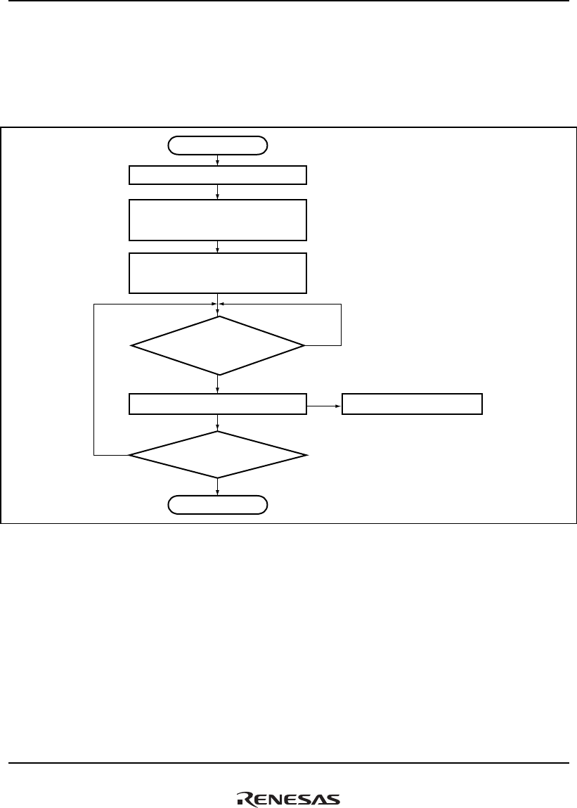
23. Serial Peripheral Interface (HSPI)
Rev.1.00 Jan. 10, 2008 Page 1165 of 1658
REJ09B0261-0100
23.4 Operation
23.4.1 Operation Overview with FIFO Mode Disabled
Figure 23.2 shows the flow of a transmit/receive operation procedure.
Yes
No
No
Yes
Start
Reset the system
Select master or slave
operation by setting the MASL bit
in SPSCR
Select required interrupts by
setting TFIE and ROIE bits in
SPSCR
Check if
SPTBR is empty by
reading the TXFL bit
in SPSR
Write data to SPTBR TX/RX data to/from slave
Another
transmit required?
End
Figure 23.2 Operational Flowchart
Depending on the settings of SPCR, the master transmits data to the slave on either the falling or
rising edge of HSPI_CLK and samples data from the slave at the opposite edge. The data transfer
between the master and slave is completed when the transmit complete status flag (TXFN) in
SPSR is set to 1. This flag should be used to identify when an HSPI transfer event (byte
transmitted and byte received) has occurred, even in the case where the HSPI module is used to
receive data only (null data being transmitted). By default data is transmitted MSB first, but LSB
first is also possible depending on how the LMSB bit in SPSCR is set.
During the transmit operation the slave responds by sending data to the master synchronized with
the HSPI_CLK from the master transmitted. Data from the slave is sampled and transferred to the
shift register in the module and on completion of the transmit operation, is transferred to SPRBR.

23. Serial Peripheral Interface (HSPI)
Rev.1.00 Jan. 10, 2008 Page 1166 of 1658
REJ09B0261-0100
The HSPI_CS pin should be used to select the HSPI module and prepare it to receive data from an
external master when the HSPI is configured as a slave. When the FBS bit in SPCR is 0, the
HSPI_CS pin must be driven high between successive bytes (the HSPI_CS pin must be driven
high after a byte transfer). When FBS = 1, the HSPI_CS pin can stay low for several byte
transmissions. In this case, if the system is configured such that FBS is always 1, the HSPI_CS
line can be fixed at ground (if the HSPI will only be used as a slave).
23.4.2 Operation with FIFO Mode Enabled
In order to reduce the interrupt overhead on the CPU, FIFO mode has been provided. When FIFO
mode is enabled, up to eight bytes can be written in advance for transmission and up to eight bytes
can be received before the receive FIFO needs to be read. To transfer the specified amount of data
between the HSPI module and an external device, use the following procedure:
1. Set up the module for the required HSPI transfer characteristics (master/slave, clock polarity
etc.) and enable FIFO mode.
2. Write bytes into the transmit FIFO via SPTBR. If more than eight bytes are to be transmitted,
enable the transmit FIFO halfway interrupt to keep track of the FIFO level as data is
transmitted.
3. Respond to the transmit FIFO halfway interrupt when it occurs by writing more data to the
transmit FIFO and reading data from the receive FIFO via SPRBR.
4. When all of the transmit data has been written into the transmit FIFO, disable the transmit
FIFO halfway interrupt and read the contents of the receive FIFO until it is empty. Enable the
receive FIFO not empty interrupt to keep track of when the final bytes of the transfer are
received.
5. Respond to the receive FIFO not empty interrupt until all the expected data has been received.
6. Disable the module until it is required again.
In some applications, an undefined amount of data will be received from an external HSPI device.
If this is the case, use the following procedure:
1. Set up the module for the required HSPI transfer characteristics (master/slave, clock polarity,
etc.) and enable FIFO mode.
2. Fill the transmit FIFO with the data to transmit. Enable the receive FIFO not empty interrupt.
3. Respond to the receive FIFO not empty interrupt and read data from the receive FIFO until it is
empty. Write more data to the transmit FIFO if required.
4. Disable the module when the transfer is to stop.
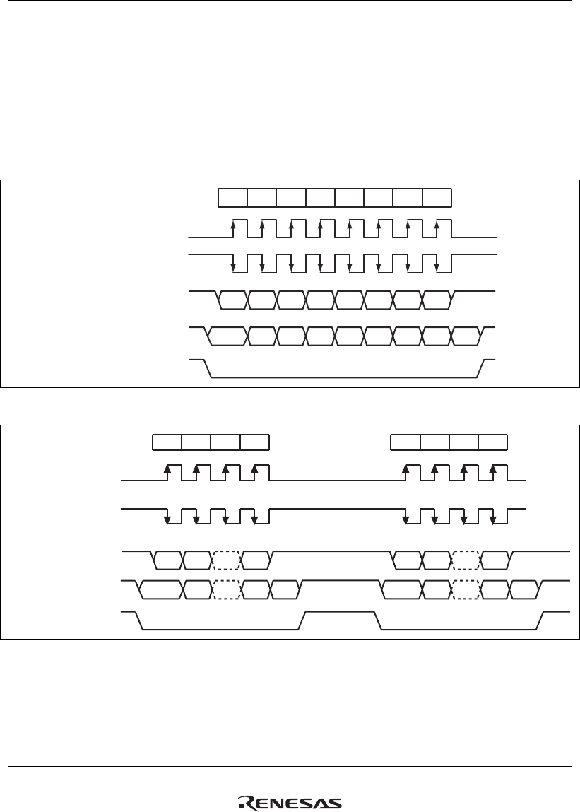
23. Serial Peripheral Interface (HSPI)
Rev.1.00 Jan. 10, 2008 Page 1167 of 1658
REJ09B0261-0100
23.4.3 Timing Diagrams
The following diagrams explain the timing relationship of all shift and sample processes in the
HSPI. Figure 23.3 shows the conditions when FBS = 0, figure 23.4 shows the conditions when
FBS = 0 (continuous transfer), figure 23.5 shows the conditions when FBS = 1, and figure 23.6
shows the conditions when FBS = 1 (continuous transfer). It can be seen that if CLKP in SPCR is
0, transmit data is shifted at the falling edge of HSPI_CLK and receive data is sampled at the
rising edge of HSPI_CLK. The opposite is true when CLKP = 1.
Data transfer cycle
HSPI_CLK (CLKP = 0)
HSPI_CLK (CLKP = 1)
1 432 8765
HSPI_TX MSB 6 5 4 3 2 1 LSB
MSB 6 5 4 3 2 1 LSB *HSPI_RX
HSPI_CS
Figure 23.3 Timing Conditions when FBS = 0
HSPI_CLK (CLKP = 0)
HSPI_CLK (CLKP = 1)
1 8..2 9 16..10
HSPI_TX MSB 6 LSB MSB 6 LSB
MSB 6 LSB MSB 6 LSB *
HSPI_RX
HSPI_CS
Data transfer cycle
*
Figure 23.4 Timing Conditions when FBS = 0 (Continuous Transfer)
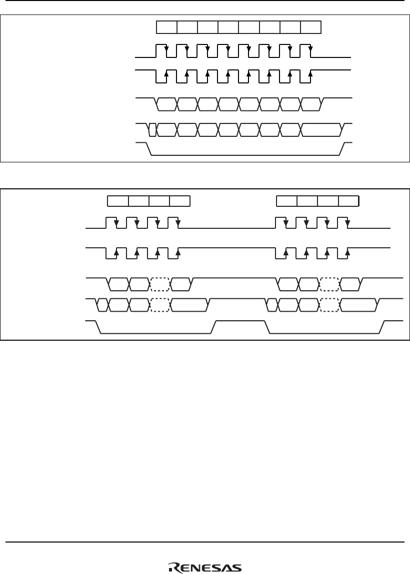
23. Serial Peripheral Interface (HSPI)
Rev.1.00 Jan. 10, 2008 Page 1168 of 1658
REJ09B0261-0100
Data transfer cycle
HSPI_CLK (CLKP = 0)
HSPI_CLK (CLKP = 1)
1 432 8765
MSB 6 5 4 3 2 1 LSB
MSB 6 5 4 3 2 1 LSB
*
HSPI_TX
HSPI_RX
HSPI_CX
Figure 23.5 Timing Conditions when FBS = 1
HSPI_CLK (CLKP = 0)
HSPI_CLK (CLKP = 1)
1 8..2 9 16..10
HSPI_TX MSB 6 LSB MSB 6 LSB
MSB 6 LSB MSB 6* * LSB
HSPI_RX
HSPI_CS
Data transfer cycle
Figure 23.6 Timing Conditions when FBS = 1 (Continuous Transfer)
The asterisk (*) in the figures shows 0 or 1.

23. Serial Peripheral Interface (HSPI)
Rev.1.00 Jan. 10, 2008 Page 1169 of 1658
REJ09B0261-0100
23.4.4 HSPI Software Reset
If any of the control bits, except for SPCR and the interrupt and chip select value bits of SPSCR,
are changed, then the HSPI software reset is generated. The receive and transmit FIFO pointers
can be initialized by the HSPI software reset. The data transmission after the HSPI software reset
should conform to transmitting and receiving protocol of HSPI and be performed from the
beginning; otherwise, correct operation is not guaranteed.
When asserting the HSPI_CS except when the master device is transferring data with the HSPI in
slave mode, set CSA again after a software reset. This prevents the HSPI from receiving erroneous
data.
23.4.5 Clock Polarity and Transmit Control
SPCR also allows the user to define the shift timing for transmit data and polarity. The FBS bit in
SPCR allows selection between two different transfer formats. When CSA of SPSR is 0, the MSB
or LSB is valid at the falling edge of HSPI_CS. The CLKP bit in SPCR allows for control of the
polarity select block, shown in figure 23.1, which selects the edge of HSPI_CLK on which data is
shifted and sampled in the master and slave.
23.4.6 Transmit and Receive Routines
The master and slave can be considered linked together as a circular shift register synchronized
with HSPI_CLK. The transmit byte from the master is replaced with the receive byte from the
slave in eight HSPI_CLK cycles. Both the transmit and receive functions are double buffered to
allow for continuous reads and writes. When FIFO mode is enabled, 8-entry FIFOs are available
for both transmit and receive data.
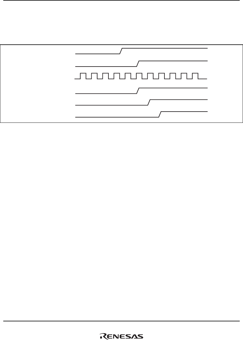
23. Serial Peripheral Interface (HSPI)
Rev.1.00 Jan. 10, 2008 Page 1170 of 1658
REJ09B0261-0100
23.4.7 Flags and Interrupt Timing
The interrupt timing when the flags of the status register (SPSR) and the system control register
(SPSCR) are set is shown in figure 23.7.
HSPI_CLK
HSPI_CS
Pck
Internal interrupt
Flags (SPSR)
Interrupt
Figure 23.7 Flags and Interrupt Timing
If an interrupt cause (receive FIFO halfway, etc.) occurs, it is reflected to the status register
(SPSR) in synchronization with Pck, and an interrupt occurs.
23.4.8 Low-Power Consumption and Clock Synchronization
The HSPI operates in synchronization with the bus clock. Module standby mode is
enabled/disabled by the MSTP2 bit of the CPG module standby control register 0 (MSTPCR0).
Take the following steps to enter module standby mode.
1. Check that all data transfers have been completed. The transmit buffer (or FIFO) must be
empty and the receive buffer (or FIFO) must be read until the receive buffer becomes empty.
2. Disable all DMA requests, interrupt requests, and FIFO mode.
3. Set the MSTP2 bit of the standby control register 0 (MSTPCR0).
To activate the HSPI, write 0 to the MSTP2 bit of the standby control register 0 (MSTPCR0).

24. Multimedia Card Interface (MMCIF)
Rev.1.00 Jan. 10, 2008 Page 1171 of 1658
REJ09B0261-0100
Section 24 Multimedia Card Interface (MMCIF)
This LSI supports a multimedia card interface (MMCIF). The MMC mode interface can be
utilized. The MMCIF is a clock-synchronous serial interface that transmits/receives data that is
distinguished in terms of command and response. A number of commands/responses are
predefined in the multimedia card. As the MMCIF specifies a command code and command
type/response type upon the issuance of a command, commands extended by the secure
multimedia card (Secure-MMC) and additional commands can be supported in the future within
the range of combinations of currently defined command types/response types.
24.1 Features
The MMCIF has the following features:
• Supports a subset of the MultiMediaCard System Specification Version 3.1
• Supports MMC mode
• Incorporates 64 data-transfer FIFOs of 16 bits
• Supports DMA transfer
• Four interrupt sources
FIFO empty/full (FSTAT), command/response/data transfer complete (TRAN), transfer error
(ERR), and FIFO ready (FRDY)
• Interface via the MMCCLK output (transfer clock output) pin, the MMCCMD input/output
(command output/response input) pin, and the MMCDAT input/output (data input/output) pin
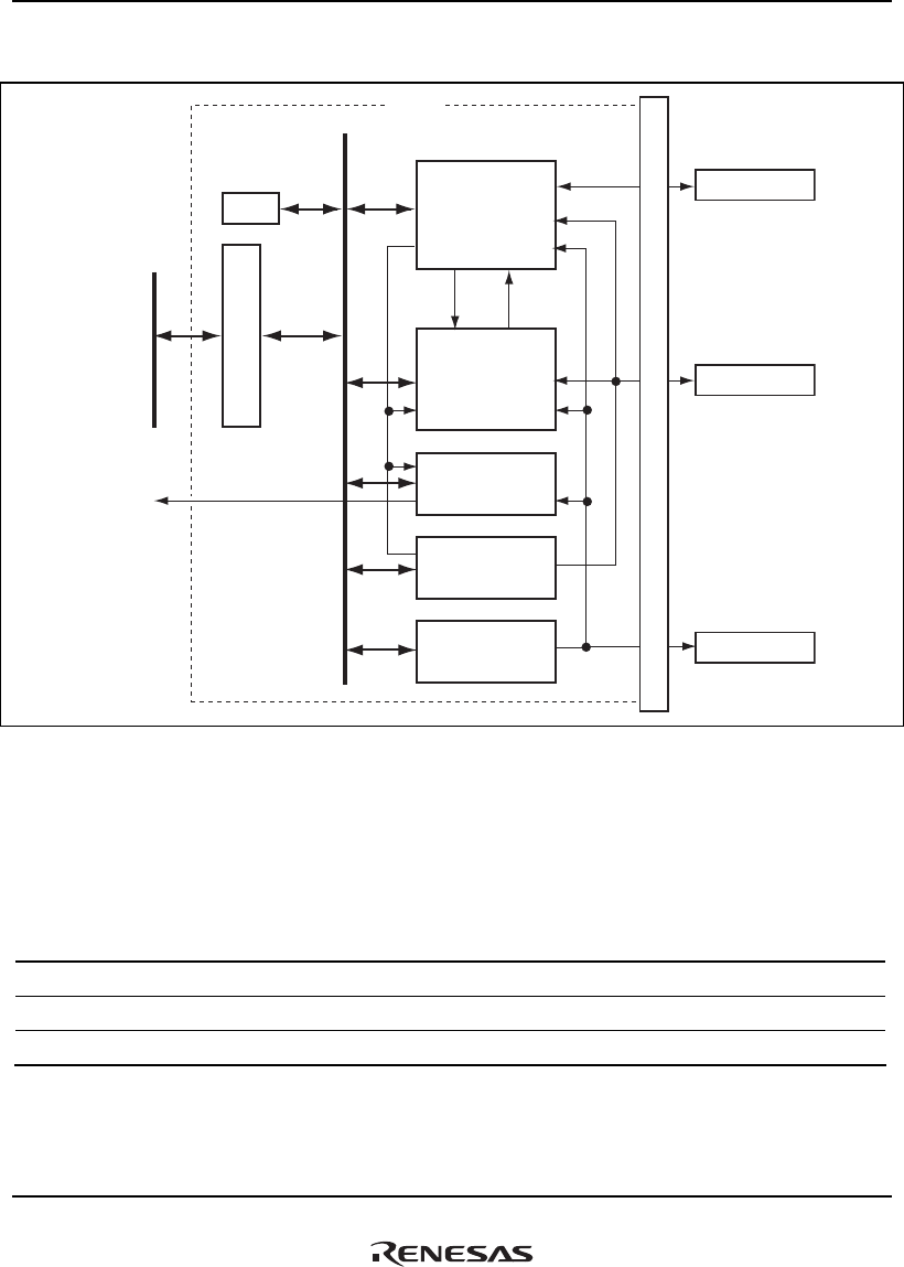
24. Multimedia Card Interface (MMCIF)
Rev.1.00 Jan. 10, 2008 Page 1172 of 1658
REJ09B0261-0100
Figure 24.1 shows a block diagram of the MMCIF.
MMCDAT
MMCCMD
MMCCLK
MMCIF
FIFO
FS TAT
TRAN
ERR
FRDY
Peripheral bus
Peripheral bus interface
Data transmission/
reception control
Command
transmission/
response
reception control
Interrupt control
MMC mode control
Card clock
generator
Port
Figure 24.1 Block Diagram of MMCIF
24.2 Input/Output Pins
Table 24.1 summarizes the pins of the MMCIF.
Table 24.1 Pin Configuration
Pin Name I/O Function
MMCCLK Input/Output Card clock output
MMCCMD Input/Output Command output/response input
MMCDAT Input/Output Data input/output
Note: For insertion/detachment of a card or for signals switching over between open-drain and
CMOS modes, use ports of this LSI.

24. Multimedia Card Interface (MMCIF)
Rev.1.00 Jan. 10, 2008 Page 1173 of 1658
REJ09B0261-0100
24.3 Register Descriptions
Table 24.2 shows the MMCIF register configuration.
Table 24.2 Register Configuration (1)
Register Name Abbrev. R/W P4 Address Area 7 Address Size
Sync
Clock
Command register 0 CMDR0 R/W H'FFE6 0000 H'1FE6 0000 8 Pck
Command register 1 CMDR1 R/W H'FFE6 0001 H'1FE6 0001 8 Pck
Command register 2 CMDR2 R/W H'FFE6 0002 H'1FE6 0002 8 Pck
Command register 3 CMDR3 R/W H'FFE6 0003 H'1FE6 0003 8 Pck
Command register 4 CMDR4 R/W H'FFE6 0004 H'1FE6 0004 8 Pck
Command register 5 CMDR5 R H'FFE6 0005 H'1FE6 0005 8 Pck
Command start register CMDSTRT R/W H'FFE6 0006 H'1FE6 0006 8 Pck
Operation control register OPCR R/W H'FFE6 000A H'1FE6 000A 8 Pck
Card status register CSTR R H'FFE6 000B H'1FE6 000B 8 Pck
Interrupt control register 0 INTCR0 R/W H'FFE6 000C H'1FE6 000C 8 Pck
Interrupt control register 1 INTCR1 R/W H'FFE6 000D H'1FE6 000D 8 Pck
Interrupt status register 0 INTSTR0 R/W H'FFE6 000E H'1FE6 000E 8 Pck
Interrupt status register 1 INTSTR1 R/W H'FFE6 000F H'1FE6 000F 8 Pck
Transfer clock control register CLKON R/W H'FFE6 0010 H'1FE6 0010 8 Pck
Command timeout control register CTOCR R/W H'FFE6 0011 H'1FE6 0011 8 Pck
Transfer byte number count register TBCR R/W H'FFE6 0014 H'1FE6 0014 8 Pck
Mode register MODER R/W H'FFE6 0016 H'1FE6 0016 8 Pck
Command type register CMDTYR R/W H'FFE6 0018 H'1FE6 0018 8 Pck
Response type register RSPTYR R/W H'FFE6 0019 H'1FE6 0019 8 Pck
Transfer block number counter TBNCR R/W H'FFE6 001A H'1FE6 001A 16 Pck
Response register 0 RSPR0 R/W H'FFE6 0020 H'1FE6 0020 8 Pck
Response register 1 RSPR1 R/W H'FFE6 0021 H'1FE6 0021 8 Pck
Response register 2 RSPR2 R/W H'FFE6 0022 H'1FE6 0022 8 Pck
Response register 3 RSPR3 R/W H'FFE6 0023 H'1FE6 0023 8 Pck
Response register 4 RSPR4 R/W H'FFE6 0024 H'1FE6 0024 8 Pck

24. Multimedia Card Interface (MMCIF)
Rev.1.00 Jan. 10, 2008 Page 1174 of 1658
REJ09B0261-0100
Register Name Abbrev. R/W P4 Address Area 7 Address Size
Sync
Clock
Response register 5 RSPR5 R/W H'FFE6 0025 H'1FE6 0025 8 Pck
Response register 6 RSPR6 R/W H'FFE6 0026 H'1FE6 0026 8 Pck
Response register 7 RSPR7 R/W H'FFE6 0027 H'1FE6 0027 8 Pck
Response register 8 RSPR8 R/W H'FFE6 0028 H'1FE6 0028 8 Pck
Response register 9 RSPR9 R/W H'FFE6 0029 H'1FE6 0029 8 Pck
Response register 10 RSPR10 R/W H'FFE6 002A H'1FE6 002A 8 Pck
Response register 11 RSPR11 R/W H'FFE6 002B H'1FE6 002B 8 Pck
Response register 12 RSPR12 R/W H'FFE6 002C H'1FE6 002C 8 Pck
Response register 13 RSPR13 R/W H'FFE6 002D H'1FE6 002D 8 Pck
Response register 14 RSPR14 R/W H'FFE6 002E H'1FE6 002E 8 Pck
Response register 15 RSPR15 R/W H'FFE6 002F H'1FE6 002F 8 Pck
Response register 16 RSPR16 R/W H'FFE6 0030 H'1FE6 0030 8 Pck
CRC status register RSPRD R/W H'FFE6 0031 H'1FE6 0031 8 Pck
Data timeout register DTOUTR R/W H'FFE6 0032 H'1FE6 0032 16 Pck
Data register DR R/W H'FFE6 0040 H'1FE6 0040 16 Pck
FIFO pointer clear register FIFOCLR W H'FFE6 0042 H'1FE6 0042 8 Pck
DMA control register DMACR R/W H'FFE6 0044 H'1FE6 0044 8 Pck
Interrupt control register 2 INTCR2 R/W H'FFE6 0046 H'1FE6 0046 8 Pck
Interrupt status register 2 INTSTR2 R/W H'FFE6 0048 H'1FE6 0048 8 Pck

24. Multimedia Card Interface (MMCIF)
Rev.1.00 Jan. 10, 2008 Page 1175 of 1658
REJ09B0261-0100
Table 24.3 Register Configuration (2)
Register Name Abbrev.
Power-on
Reset by
PRESET
Pin/WDT/
H-UDI
Manual
Reset by WDT/
Multiple
Exception
Sleep by
SLEEP
Instruction
Module
Standby
Command register 0 CMDR0 H'00 H'00 Retained Retained
Command register 1 CMDR1 H'00 H'00 Retained Retained
Command register 2 CMDR2 H'00 H'00 Retained Retained
Command register 3 CMDR3 H'00 H'00 Retained Retained
Command register 4 CMDR4 H'00 H'00 Retained Retained
Command register 5 CMDR5 H'00 H'00 Retained Retained
Command start register CMDSTRT H'00 H'00 Retained Retained
Operation control register OPCR H'00 H'00 Retained Retained
Card status register CSTR H'0x H'0x Retained Retained
Interrupt control register 0 INTCR0 H'00 H'00 Retained Retained
Interrupt control register 1 INTCR1 H'00 H'00 Retained Retained
Interrupt status register 0 INTSTR0 H'00 H'00 Retained Retained
Interrupt status register 1 INTSTR1 H'00 H'00 Retained Retained
Transfer clock control register CLKON H'00 H'00 Retained Retained
Command timeout control register CTOCR H'01 H'01 Retained Retained
Transfer byte number count register TBCR H'00 H'00 Retained Retained
Mode register MODER H'00 H'00 Retained Retained
Command type register CMDTYR H'00 H'00 Retained Retained
Response type register RSPTYR H'00 H'00 Retained Retained
Transfer block number counter TBNCR H'0000 H'0000 Retained Retained
Response register 0 RSPR0 H'00 H'00 Retained Retained
Response register 1 RSPR1 H'00 H'00 Retained Retained
Response register 2 RSPR2 H'00 H'00 Retained Retained
Response register 3 RSPR3 H'00 H'00 Retained Retained
Response register 4 RSPR4 H'00 H'00 Retained Retained
Response register 5 RSPR5 H'00 H'00 Retained Retained

24. Multimedia Card Interface (MMCIF)
Rev.1.00 Jan. 10, 2008 Page 1176 of 1658
REJ09B0261-0100
Register Name Abbrev.
Power-on
Reset by
PRESET
Pin/WDT/
H-UDI
Manual Reset
by WDT/
Multiple
Exception
Sleep by
SLEEP
Instruction
Module
Standby
Response register 6 RSPR6 H'00 H'00 Retained Retained
Response register 7 RSPR7 H'00 H'00 Retained Retained
Response register 8 RSPR8 H'00 H'00 Retained Retained
Response register 9 RSPR9 H'00 H'00 Retained Retained
Response register 10 RSPR10 H'00 H'00 Retained Retained
Response register 11 RSPR11 H'00 H'00 Retained Retained
Response register 12 RSPR12 H'00 H'00 Retained Retained
Response register 13 RSPR13 H'00 H'00 Retained Retained
Response register 14 RSPR14 H'00 H'00 Retained Retained
Response register 15 RSPR15 H'00 H'00 Retained Retained
Response register 16 RSPR16 H'00 H'00 Retained Retained
CRC status register RSPRD H'00 H'00 Retained Retained
Data timeout register DTOUTR H'FFFF H'FFFF Retained Retained
Data register DR H'xxxx H'xxxx Retained Retained
FIFO pointer clear register FIFOCLR H'00 H'00 Retained Retained
DMA control register DMACR H'00 H'00 Retained Retained
Interrupt control register 2 INTCR2 H'00 H'00 Retained Retained
Interrupt status register 2 INTSTR2 H'0x H'0x Retained Retained

24. Multimedia Card Interface (MMCIF)
Rev.1.00 Jan. 10, 2008 Page 1177 of 1658
REJ09B0261-0100
24.3.1 Command Registers 0 to 5 (CMDR0 to CMDR5)
The CMDR registers are six 8-bit registers. A command is written to CMDR as shown in table
24.4, and the command is transmitted when the CMDSTART bit in CMDSTRT is set to 1. Each
command is transmitted in order form the MSB (bit 7) in CMDR0 to the LSB (bit 0) in CMDR5.
Table 24.4 CMDR Configuration
Register Contents Operation
CMDR0 to
CMDR4
Command argument Write command arguments.
CMDR5 CRC and End bit Setting of CRC is unnecessary (automatic calculation).
End bit is fixed to 1 and its setting is unnecessary
(automatic setting).
The read value is 0.
(1) CMDR0 to CMDR4
Bit:
Initial value:
R/W:
76543210
0000
(command argument)
0000
R/W R/W R/W R/W R/W R/W R/W R/W
Bit Bit Name
Initial
Value R/W Description
7 to 0 — All 0 R/W Command arguments
See specifications for the MMC card.
Data is sequentially transmitted from CMDR0 MSB to
CMDR5 LSB.

24. Multimedia Card Interface (MMCIF)
Rev.1.00 Jan. 10, 2008 Page 1178 of 1658
REJ09B0261-0100
(2) CMDR5
Bit:
Initial value:
R/W:
76543210
00000000
R
CRC End
RR RR RRR
Bit Bit Name
Initial
Value R/W Description
7 to 1 CRC All 0 R These bits are always read as 0. The write value should
always be 0.
0 End 0 R This bit is always read as 0. The write value should
always be 0.
24.3.2 Command Start Register (CMDSTRT)
CMDSTRT is an 8-bit readable/writable register that triggers the start of command transmission,
representing the start of a command sequence. The following operations should have been
completed before the command sequence starts.
• Analysis of prior command response, clearing the command response register write if
necessary
• Analysis/transfer of receive data of prior command if necessary
• Preparation of transmit data of the next command if necessary
• Setting of CMDTYR, RSPTYR, TBCR and TBNCR
• Setting of CMDR0 to CMDR4
The CMDR0 to CMDR4, CMDTYR, RSPTYR, TBCR and TBNCR registers should not be
changed until command transmission has ended (during the CWRE flag in CSTR has been set
to 1 or until command transmit end interrupt has occurred).
Command sequences are controlled by the sequencers in both the MMCIF side and the MMC card
side. Normally, these operate synchronously. However, if an error occurs or a command is
aborted, these may become temporarily unsynchronized. Be careful when setting the CMDOFF bit
in OPCR, issuing the CMD12 command, or processing an error in MMC mode. A new command
sequence should be started only after the end of the command sequence on both the MMCIF and
card sides is confirmed. See section24.4, Operation when an error occurred.

24. Multimedia Card Interface (MMCIF)
Rev.1.00 Jan. 10, 2008 Page 1179 of 1658
REJ09B0261-0100
Bit:
Initial value:
R/W:
76543210
00000000
R
CMD
START
RRRRRRR/W
⎯⎯⎯⎯⎯⎯⎯
Bit Bit Name
Initial
Value R/W Description
7 to 1 — All 0 R Reserved
These bits are always read as 0. The write value should
always be 0.
0 CMDSTART 0 R/W Starts command transmission when 1 is written. This bit
is automatically cleared to 0 after the MMCIF received
the CMDSTART command. When 0 is written to this bit,
operation is not affected.
24.3.3 Operation Control Register (OPCR)
OPCR is an 8-bit readable/writable register that aborts command operation, and suspends or
continues data transfer.
Bit:
Initial value:
R/W:
76543210
00000000
R/W
DATAEN
RD_
CONTI
CMD
OFF
R R/W R/W R R R R
⎯⎯⎯⎯⎯
Bit Bit Name
Initial
Value R/W Description
7 CMDOFF 0 R/W Command Off
Aborts all command operations (MMCIF command
sequence) when 1 is written after a command is
transmitted. This bit is cleared to 0 automatically after
the MMCIF received the CMDOFF command.
Write enabled period: From command transmission
completion to command sequence end
Write of 0: Operation is not affected.
Write of 1: Command sequence is forcibly aborted.
Note: Do not write to this bit out of the write enable
period.

24. Multimedia Card Interface (MMCIF)
Rev.1.00 Jan. 10, 2008 Page 1180 of 1658
REJ09B0261-0100
Bit Bit Name
Initial
Value R/W Description
6 — 0 R Reserved
This bit is always read as 0. The write value should
always be 0.
5 RD_CONTI 0 R/W Read Continue
Read data reception is resumed when 1 is written while
the sequence has been halted by FIFO full or
termination of block reading in multiple block read.
This bit is cleared to 0 automatically when 1 is written
and the MMCIF received the RD_CONTI command.
Write enabled period: While read data reception is
halted
Write of 0: Operation is not affected.
Write of 1: Resumes read data reception.
Note: Do not write to this bit out of the write enable
period.
4 DATAEN 0 R/W Data Enable
Starts a write data transmission by a command with
write data. This bit is cleared automatically when 1 is
written and the MMCIF received the DATAEN
command. Resumes write data transmission while the
sequence has been halted by FIFO empty or
termination of block writing in multiple block write.
Write enabled period: (1) after receiving a response to a
command with write data, (2) while sequence is halted
by FIFO empty, (3) when one block writing in multiple
block write is terminated.
Write of 0: Operation is not affected.
Write of 1: Starts or resumes write data transmission.
Note: Do not write to this bit out of the write enable
period.
3 to 0 — All 0 R Reserved
These bits are always read as 0. The write value should
always be 0.

24. Multimedia Card Interface (MMCIF)
Rev.1.00 Jan. 10, 2008 Page 1181 of 1658
REJ09B0261-0100
In write data transmission, the contents of the command response and data response should be
analyzed, and then transmission should be triggered. In addition, the data transmission should be
temporarily halted by FIFO full/empty, and it should be resumed when the preparation has been
completed.
In multiple block transfer, the transfer should be temporarily halted at every block break to select
either to continue to the next block or to abort the multiple block transfer command by issuing the
CMD12 command. To continue to the next block, the RD_CONTI and DATAEN bits should be
set to 1. To issue the CMD12 command, the CMDOFF bit should be set to 1 to abort the command
sequence on the MMCIF side. When using the auto-mode for a pre-defined multiple block
transfer, the setting of the RD_CONTI bit or the DATAEN bit between blocks can be omitted.
24.3.4 Card Status Register (CSTR)
CSTR indicates the MMCIF status during command sequence execution.
Bit:
Initial value:
R/W:
76543210
00000 00
R
DTBUSY DTBUSY
_TU REQBUSY CWRE
FIFO_
FULL
FIFO_
EMPTY
RR RR RRR
—
—
Bit Bit Name
Initial
Value R/W Description
7 BUSY 0 R Command Busy
Indicates command execution status. When the
CMDOFF bit in OPCR is set to 1, this bit is cleared to 0
because the MMCIF command sequence is aborted.
0: Idle state waiting for a command, or data busy state
1: Command sequence execution in progress
6 FIFO_FULL 0 R FIFO Full
This bit is set to 1 when the FIFO becomes full while
data is being received from the card, and cleared to 0
when RD_CONTI is set to 1 or the command sequence
is completed.
Indicates whether the FIFO is empty or not.
0: The FIFO is empty.
1: The FIFO is full.

24. Multimedia Card Interface (MMCIF)
Rev.1.00 Jan. 10, 2008 Page 1182 of 1658
REJ09B0261-0100
Bit Bit Name
Initial
Value R/W Description
5 FIFO_EMPTY 0 R FIFO Empty
This bit is set to 1 when the FIFO becomes empty while
data is being sent to the card, and cleared to 0 when
DATA_EN is set to 1 or the command sequence is
completed.
Indicates whether the FIFO holds data or not.
0: The FIFO includes data.
1: The FIFO is empty.
4 CWRE 0 R Command Register Write Enable
Indicates whether the CMDR command is being
transmitted or has been transmitted.
0: The CMDR command has been transmitted, or the
CMDSTART bit in CMDSTRT has not been set yet,
so the new command can be written.
1: The CMDR command is waiting for transmission or is
being transmitted. If a new command is written, a
malfunction will result.
3 DTBUSY 0 R Data Busy
Indicates command execution status. Indicates that the
card is in the busy state after the command sequence
of a command without data transfer which includes the
busy state in the response, or a command with write
data has been ended.
0: Idle state waiting for a command, or command
sequence execution in progress
1: Card is in the data busy state after command
sequence termination.
2 DTBUSY_TU Undefined R Data Busy Pin Status
Indicates the MMCDAT pin level. By reading this bit, the
MMCDAT level can be monitored.
0: A low level is input to the MMCDAT pin.
1: A high level is input to the MMCDAT pin.
1 — 0 R Reserved
This bit is always read as 0. The write value should
always be 0.

24. Multimedia Card Interface (MMCIF)
Rev.1.00 Jan. 10, 2008 Page 1183 of 1658
REJ09B0261-0100
Bit Bit Name
Initial
Value R/W Description
0 REQ 0 R Interrupt Request
Indicates whether an interrupt is requested or not.
When any of the INTSTR0, INTSTR1 and INTSTR2
flags is set, this bit is set to 1. Setting of the INTSTR0,
INTSTR1 and INTSTR2 flags is controlled by the
enable bits in INTCR0, INTSTR1 and INTCR2.
0: No interrupt requested.
1: Interrupt requested.
24.3.5 Interrupt Control Registers 0 to 2 (INTCR0 to INTCR2)
The INTCR registers enable or disable interrupts.
(1) INTCR0
Bit:
Initial value:
R/W:
76543210
00000 000
R/W
FEIE FFIE DRPIE DTIE CRPIE CMDIE DBS
YIE
R/W R/W R/W R/W R/W R/W R/W
BTIE
Bit Bit Name
Initial
Value R/W Description
7 FEIE 0 R/W FIFO Empty Interrupt Flag Setting Enable
0: Disables FIFO empty interrupt (disables FEI flag
setting).
1. Enables FIFO empty interrupt (enables FEI flag
setting).
6 FFIE 0 R/W FIFO Full Interrupt Flag Setting Enable
0: Disables FIFO full interrupt (disables FFI flag
setting).
1: Enables FIFO full interrupt (enables FFI flag setting).
5 DRPIE 0 R/W Data Response Interrupt Flag Setting Enable
0: Disables data response interrupt (disables DPRI flag
setting).
1: Enables data response interrupt (enables DPRI flag
setting).

24. Multimedia Card Interface (MMCIF)
Rev.1.00 Jan. 10, 2008 Page 1184 of 1658
REJ09B0261-0100
Bit Bit Name
Initial
Value R/W Description
4 DTIE 0 R/W Data Transfer End Interrupt Flag Setting Enable
0: Disables data transfer end interrupt (disables DTI
flag setting).
1: Enables data transfer end interrupt (enables DTI flag
setting).
3 CRPIE 0 R/W Command Response Receive End Interrupt Flag
Setting Enable
0: Disables command response receive end interrupt
(disables CRPI flag setting).
1: Enables command response receive end interrupt
(enables CRPI flag setting).
2 CMDIE 0 R/W Command Transmit End Interrupt Flag Setting Enable
0: Disables command transmit end interrupt (disables
CMDI flag setting).
1: Enables command transmit end interrupt (enables
CMDI flag setting).
1 DBSYIE 0 R/W Data Busy End Interrupt Flag Setting Enable
0: Disables data busy end interrupt (disables DBSYI
flag setting).
1: Enables data busy end interrupt (enables DBSYI flag
setting).
0 BTIE 0 R/W Multiple block Transfer End Flag Setting Enable
0: Disables multiple block transfer end flag setting
1: Enables multiple block transfer end flag setting

24. Multimedia Card Interface (MMCIF)
Rev.1.00 Jan. 10, 2008 Page 1185 of 1658
REJ09B0261-0100
(2) INTCR1
Bit:
Initial value:
R/W:
76543210
00000 000
R/W
INTR
Q2E
INTR
Q1E
INTR
Q0E
CRCE
RIE
DTE
RIE
CTE
RIE
R/W R/W R R R/W R/W R/W
⎯⎯
Bit Bit Name
Initial
Value R/W Description
7 INTRQ2E 0 R/W ERR Interrupt Enable
0: Disables ERR interrupt.
1: Enables ERR interrupt.
6 INTRQ1E 0 R/W TRAN Interrupt Enable
0: Disables TRAN interrupt.
1: Enables TRAN interrupt.
5 INTRQ0E 0 R/W FSTAT Interrupt Enable
0: Disables FSTAT interrupt.
1: Enables FSTAT interrupt.
4, 3 — All 0 R Reserved
These bits are always read as 0. The write value should
always be 0.
2 CRCERIE 0 R/W CRC Error Interrupt Flag Setting Enable
0: Disables CRC error interrupt (disables CRCERI flag
setting).
1: Enables CRC error interrupt (enables CRCERI flag
setting).
1 DTERIE 0 R/W Data Timeout Error Interrupt Flag Setting Enable
0: Disables data timeout error interrupt (disables DTERI
flag setting).
1: Enables data timeout error interrupt (enables DTERI
flag setting).
0 CTERIE 0 R/W Command Timeout Error Interrupt Flag Setting Enable
0: Disables command timeout error interrupt (disables
CTERI flag setting).
1: Enables command timeout error interrupt (enables
CTERI flag setting).

24. Multimedia Card Interface (MMCIF)
Rev.1.00 Jan. 10, 2008 Page 1186 of 1658
REJ09B0261-0100
(3) INTCR2
Bit:
Initial value:
R/W:
76543210
00000 000
R/W
FRDYIE
R R R R R R R/W
⎯⎯⎯⎯⎯⎯
INTR
Q3E
Bit Bit Name
Initial
Value R/W Description
7 INTRQ3E 0 R/W FRDY Interrupt Enable
0: Disables FRDY interrupt.
1: Enables FRDY interrupt.
6 to 1 ⎯ All 0 R Reserved
These bits are always read as 0. The write value should
always be 0.
0 FRDYIE 0 R/W FIFO Ready Interrupt Enable
0: Disables FIFO ready interrupt (disables FRDY flag
setting).
1: Enables FIFO ready interrupt (enables FRDY flag
setting).

24. Multimedia Card Interface (MMCIF)
Rev.1.00 Jan. 10, 2008 Page 1187 of 1658
REJ09B0261-0100
24.3.6 Interrupt Status Registers 0 to 2 (INTSTR0 to INTSTR2)
The INTSTR registers enable or disable MMCIF interrupts FSTAT, TRAN, ERR and FRDY, and
interrupt flags.
(1) INTSTR0
Bit:
Initial value:
R/W:
76543210
00000 000
R/W
FEI FFI DRPI DTI CRPI CMDI DBSYI
R/W R/W R/W R/W R/W R/W R/W
BTI
Bit Bit Name
Initial
Value R/W Description
Interrupt
output
7 FEI 0 R/W FIFO Empty Interrupt Flag
0: No interrupt
[Clearing condition]
Write 0 after reading FEI = 1.
(Writing 1 is invalid)
1: Interrupt requested
[Setting condition]
When FIFO becomes empty while FEIE = 1
and data is being transmitted
(when the FIFO_EMPTY bit in CSTR is set)
FSTAT
6 FFI 0 R/W FIFO Full Interrupt Flag
0: No interrupt
[Clearing condition]
Write 0 after reading FFI = 1.
(Writing 1 is invalid)
1: Interrupt requested
[Setting condition]
When FIFO becomes full while FFIE = 1
and data is being received
(when the FIFO_FULL bit in CSTR is set)
FSTAT

24. Multimedia Card Interface (MMCIF)
Rev.1.00 Jan. 10, 2008 Page 1188 of 1658
REJ09B0261-0100
Bit Bit Name
Initial
Value R/W Description
Interrupt
output
5 DRPI 0 R/W Data Response Interrupt Flag
0: No interrupt
[Clearing condition]
Write 0 after reading DRPI = 1.
(Writing 1 is invalid)
1: Interrupt requested
[Setting condition]
When the CRC status is received while
DRPIE = 1.
TRAN
4 DTI 0 R/W Data Transfer End Interrupt Flag
0: No interrupt
[Clearing condition]
Write 0 after reading DTI = 1.
(Writing 1 is invalid)
1: Interrupt requested
[Setting condition]
When the number of bytes of data transfer
specified in TBCR ends while DTIE = 1.
TRAN
3 CRPI 0 R/W Command Response Receive End Interrupt
Flag
0: No interrupt
[Clearing condition]
Write 0 after reading CRPI = 1.
(Writing 1 is invalid)
1: Interrupt requested
[Setting condition]
When command response reception ends
while CRPIE = 1.
TRAN

24. Multimedia Card Interface (MMCIF)
Rev.1.00 Jan. 10, 2008 Page 1189 of 1658
REJ09B0261-0100
Bit Bit Name
Initial
Value R/W Description
Interrupt
output
2 CMDI 0 R/W Command Transmit End Interrupt Flag
0: No interrupt
[Clearing condition]
Write 0 after reading CMDI = 1.
(Writing 1 is invalid)
1: Interrupt requested
[Setting condition]
When command transmission ends while
CMDIE = 1. (When the CWRE bit in CSTR
is cleared.)
TRAN
1 DBSYI 0 R/W Data Busy End Interrupt Flag
0: No interrupt
[Clearing condition]
Write 0 after reading DBSYI = 1.
(Writing 1 is invalid)
1: Interrupt requested
[Setting condition]
When data busy state is canceled while
DBSYIE = 1. (When the DTBUSY bit in
CSTR is cleared.)
TRAN
0 BTI 0 R/W Multiple block Transfer End Flag
0: No interrupt
[Clearing condition]
Write 0 after reading BTI = 1.
(Writing 1 is invalid)
1: Interrupt requested
[Setting condition]
When the number of bytes of data transfer
specified in TBCR is reached while BTIE =
1 and TBNCR = 0.
TRAN

24. Multimedia Card Interface (MMCIF)
Rev.1.00 Jan. 10, 2008 Page 1190 of 1658
REJ09B0261-0100
(2) INTSTR1
Bit:
Initial value:
R/W:
76543210
00000 000
R
CRC
ERI DTERI CTERI
R R R R R/W R/W R/W
⎯⎯⎯⎯⎯
Bit Bit Name
Initial
Value R/W Description
Interrupt
output
7 to 3 — All 0 R Reserved
These bits are always read as 0. The write
value should always be 0.
—
2 CRCERI 0 R/W CRC Error Interrupt Flag
0: No interrupt
[Clearing condition]
Write 0 after reading CRCERI = 1.
(Writing 1 is invalid)
1: Interrupt requested
[Setting condition]
When a CRC error for command response
or receive data or a CRC status error for
transmit data response is detected while
CRCERIE = 1.
For the command response, CRC is
checked when the RTY4 in RSPTYR is
enabled.
ERR
1 DTERI 0 R/W Data Timeout Error Interrupt Flag
0: No interrupt
[Clearing condition]
Write 0 after reading DTERI = 1.
(Writing 1 is invalid)
1: Interrupt requested
[Setting condition]
When a data timeout error specified in
DTOUTR occurs while DTERIE = 1.
ERR

24. Multimedia Card Interface (MMCIF)
Rev.1.00 Jan. 10, 2008 Page 1191 of 1658
REJ09B0261-0100
Bit Bit Name
Initial
Value R/W Description
Interrupt
output
0 CTERI 0 R/W Command Timeout Error Interrupt Flag
0: No interrupt
[Clearing condition]
Write 0 after reading CTERI = 1.
(Writing 1 is invalid)
1: Interrupt requested
[Setting condition]
When a command timeout error specified in
TOCR occurs while CTERIE = 1.
ERR

24. Multimedia Card Interface (MMCIF)
Rev.1.00 Jan. 10, 2008 Page 1192 of 1658
REJ09B0261-0100
(3) INTSTR2
Bit:
Initial value:
R/W:
76543210
00000 0 0
R
FRDY
_TU FRDYI
R R R R R R R/W
——————
—
Bit Bit Name
Initial
Value R/W Description
Interrupt
output
7 to 2 ⎯ All 0 R Reserved
These bits are always read as 0. The write
value should always be 0.
⎯
1 FRDY_TU Undefined R FIFO Ready Flag
Regardless of set values of DMAEN and
FRDYIE, this bit is read as 0 when FIFO
data amount matches the asserting
condition set in DMACR[2:0], and
otherwise, read as 1.
⎯
0 FRDYI 0 R/W FIFO Ready Interrupt Flag
0: No interrupt
[Clearing condition]
Write 0 after reading FRDYI = 1.
(Writing 1 is invalid)
1: Interrupt requested
[Setting condition]
When remained FIFO data does not match
the assert condition set in DMACR while
DMAEN = 1 and FRDYIE = 1.
Note: FRDYI will be set on the setting
condition after clearing. To clear it,
disable the flag setting by FRDYIE in
INTCR2.
FRDY

24. Multimedia Card Interface (MMCIF)
Rev.1.00 Jan. 10, 2008 Page 1193 of 1658
REJ09B0261-0100
24.3.7 Transfer Clock Control Register (CLKON)
CLKON controls the transfer clock frequency and clock ON/OFF.
At this time, use a sufficiently slow clock for transfer through open-drain type output in MMC
mode.
In a command sequence, do not perform clock ON/OFF or frequency modification.
Bit:
Initial value:
R/W:
76543210
00000 000
R/W
CLKON CSEL2 CSEL1 CSEL0
R R R R/W R/W R/W R/W
⎯⎯⎯
CSEL3
Bit Bit Name
Initial
Value R/W Description
7 CLKON 0 R/W Clock On
0: Stops the transfer clock output from the MMCCLK
pin.
1: Outputs the transfer clock from the MMCCLK pin.
6 to 4 — All 0 R Reserved
These bits are always read as 0. The write value
should always be 0.
3
2
1
0
CSEL3
CSEL2
CSEL1
CSEL0
0
0
0
0
R/W
R/W
R/W
R/W
Transfer Clock Frequency Select
0000: Reserved
0001: Uses the 1/2-divided peripheral clock (Pck) as a
transfer clock.
0010: Uses the 1/4-divided peripheral clock as a
transfer clock.
0011: Uses the 1/8-divided peripheral clock as a
transfer clock.
0100: Uses the 1/16-divided peripheral clock as a
transfer clock.
0101: Uses the 1/32-divided peripheral clock as a
transfer clock.
0110: Uses the 1/64-divided peripheral clock as a
transfer clock.
0111: Uses the 1/128-divided peripheral clock as a
transfer clock.
1000: Uses the 1/256-divided peripheral clock as a
transfer clock.
1001 to 1111: Setting prohibited

24. Multimedia Card Interface (MMCIF)
Rev.1.00 Jan. 10, 2008 Page 1194 of 1658
REJ09B0261-0100
24.3.8 Command Timeout Control Register (CTOCR)
CTOCR specifies the period to generate a timeout for the command response.
The counter (CTOUTC), to which the peripheral bus does not have access, counts the transfer
clock to monitor the command timeout. The initial value of CTOUTC is 0, and CTOUTC starts
counting the transfer clock from the start of command transmission. CTOUTC is cleared and stops
counting the transfer clock when command response reception has been completed, or when the
command sequence has been aborted by setting the CMDOFF bit to 1.
When the command response cannot be received, CTOUTC continues counting the transfer clock,
and enters the command timeout error state when the number of transfer clock cycles reaches the
number specified in CTOCR. When the CTERIE bit in INTCR1 is set to 1, the CTERI flag in
INTSTR1 is set. As CTOUTC continues counting transfer clock, the CTERI flag setting condition
is repeatedly generated. To perform command timeout error handling, the command sequence
should be aborted by setting the CMDOFF bit to 1, and then the CTERI flag should be cleared to
prevent extra-interrupt generation.
Bit:
Initial value:
R/W:
76543210
00000001
R
CTSEL0
⎯
R R R R R R R/W
⎯⎯⎯⎯⎯⎯
Bit Bit Name
Initial
Value R/W Description
7 to 1 — All 0 R Reserved
These bits are always read as 0. The write value should
always be 0.
0 CTSEL0 1 R/W Command Timeout Select
0: 128 transfer clock cycles from command
transmission completion to response reception
completion
1: 256 transfer clock cycles from command
transmission completion to response reception
completion
Transfer clock: MMCCLK
Note: If R2 response (17-byte command response) is requested and CTSEL0 is cleared to 0, a
timeout is generated during response reception. Therefore, set CTSEL0 to 1.

24. Multimedia Card Interface (MMCIF)
Rev.1.00 Jan. 10, 2008 Page 1195 of 1658
REJ09B0261-0100
24.3.9 Transfer Byte Number Count Register (TBCR)
TBCR is an 8-bit readable/writable register that specifies the number of bytes to be transferred
(block size) for each single block transfer command. TBCR specifies the number of data block
bytes not including the start bit, end bit, and CRC.
The multiple block transfer command corresponds to the number of bytes of each data block. This
setting is ignored by the stream transfer command.
Bit:
Initial value:
R/W:
76543210
00000000
R
C2C3 C1 C0
R R R R/W R/W R/W R/W
⎯⎯⎯⎯
Bit Bit Name
Initial
Value R/W Description
7 to 4 — All 0 R Reserved
These bits are always read as 0. The write value should
always be 0.
3
2
1
0
CS3
CS2
CS1
CS0
0
0
0
0
R/W
R/W
R/W
R/W
Transfer Data Block Size
Four or more bytes should be set before executing a
command with data transfer.
0000: 1 byte (for forced erase)
0001: 2 bytes
0010: 4 bytes
0011: 8 bytes
0100: 16 bytes
0101: 32 bytes
0110: 64 bytes
0111: 128 bytes
1000: 256 bytes
1001: 512 bytes
1010: 1024 bytes
1011: 2048 bytes
1100 to 1111: Setting prohibited

24. Multimedia Card Interface (MMCIF)
Rev.1.00 Jan. 10, 2008 Page 1196 of 1658
REJ09B0261-0100
24.3.10 Mode Register (MODER)
MODER is an 8-bit readable/writable register that specifies the MMCIF operating mode. The
following sequence should be repeated when the MMCIF uses the multimedia card: Send a
command, wait for the end of the command sequence and the end of the data busy state, and send
a next command.
The series of operations from command sending, command response reception, data
transmission/reception, and data response reception is called as the command sequence. The
command sequence starts from sending a command by setting the CMDSTART bit in CMDSTRT
to 1, and ends when all necessary data transmission/reception and response reception have been
completed. The multimedia card supports the data busy state such that only the specific command
is accepted to write/erase data to/from the flash memory in the card during command sequence
execution and after command sequence execution has ended. The data busy state is indicated by a
low level output from the card side to the MMCDAT pin.
Bit:
Initial value:
R/W:
76543210
00000000
R
MODE
R R R R R R R/W
⎯⎯⎯⎯⎯ ⎯⎯
Bit Bit Name
Initial
Value R/W Description
7 to 1 — All 0 R Reserved
These bits are always read as 0. The write value should
always be 0.
0 MODE 0 R/W Operating Mode
Specifies the MMCIF operating mode.
0: Operates in MMC mode
1: Setting prohibited

24. Multimedia Card Interface (MMCIF)
Rev.1.00 Jan. 10, 2008 Page 1197 of 1658
REJ09B0261-0100
24.3.11 Command Type Register (CMDTYR)
CMDTYR is an 8-bit readable/writable register that specifies the command format in conjunction
with RSPTYR. Bits TY1 and TY0 specify the existence and direction of transfer data, and bits
TY6 to TY2 specify the additional settings. All of bits TY6 to TY2 should be cleared to 0 or only
one of them should be set to 1. Bits TY6 to TY2 can only be set to 1 if the corresponding settings
in TY1 and TY0 allow that setting. If these bits are not set correctly, the operation cannot be
guaranteed. When executing a single block transaction, set TY1 and TY0 to 01 or 10, and TY6 to
TY2 to all 0s.
Bit:
Initial value:
R/W:
76543210
00000000
R
TY4 TY3 TY2 TY1 TY0
R/W R/W R/W R/W R/W R/W R/W
TY6
⎯TY5
Bit Bit Name
Initial
Value R/W Description
7 to 5 ⎯ All 0 R Reserved
These bits are always read as 0. The write value should
always be 0.
6 TY6 0 R/W Type 6
Specifies a predefined multiple block transaction.
TY[1:0] should be set to 01 or 10.
When using the command set to this bit, it is necessary
to specify the transfer block size and the transfer block
number in the TBCR and TBNCR respectively.
5 TY5 0 R/W Type 5
Specifies a multiple block transaction when using
secure MMC. TY[1:0] should be set to 01 or 10.
Using the command to set to this bit, it is necessary to
specify the transfer block size and the transfer block
number in the TBCR and TBNCR respectively.
4 TY4 0 R/W Type 4
Set this bit to 1 when specifying the CMD12 command.
Bits TY1 and TY0 should be set to 00.

24. Multimedia Card Interface (MMCIF)
Rev.1.00 Jan. 10, 2008 Page 1198 of 1658
REJ09B0261-0100
Bit Bit Name
Initial
Value R/W Description
3 TY3 0 R/W Type 3
Set this bit to 1 when specifying stream transfer. Bits
TY1 and TY0 should be set to 01 or 10.
The command sequence of the stream transfer
specified by this bit ends when it is aborted by the
CMD12 command.
2 TY2 0 R/W Type 2
Set this bit to 1 when specifying a multiple block
transfer. Bits TY1 and TY0 should be set to 01 or 10.
The command sequence of the multiple block transfer
specified by this bit ends when it is aborted by the
CMD12 command.
1
0
TY1
TY0
0
0
R/W
R/W
Types 1 and 0
These bits specify the existence and direction of
transfer data.
00: A command without data transfer
01: A command with read data reception
10: A command with write data transmission
11: Setting prohibited
24.3.12 Response Type Register (RSPTYR)
RSPTYR is an 8-bit readable/writable register that specifies command format in conjunction with
CMDTYR. Bits RTY2 to RTY0 specify the number of response bytes, and bits RTY6 to RTY4
specify the additional settings.
Bit:
Initial value:
R/W:
76543210
00000000
R
RTY5 RTY4 RTY2 RTY1 RTY0
R/W R/W R/W R R/W R/W R/W
⎯⎯ RTY6
Bit Bit Name
Initial
Value R/W Description
7 ⎯ 0 R Reserved
This bit is always read as 0. The write value should
always be 0.

24. Multimedia Card Interface (MMCIF)
Rev.1.00 Jan. 10, 2008 Page 1199 of 1658
REJ09B0261-0100
Bit Bit Name
Initial
Value R/W Description
6 RTY6 0 R/W Response Type 5
Sets data busy status from the MMC card.
This bit is set to perform CRC check for the response
(R2 response of MMC mode) when the command that
reads, as a response, the register value of the
multimedia card, including CRC7, is executed.
RTY2 to RTY0 must be set to 101.
5 RTY5 0 R/W Response Type 5
Sets data busy status from the MMC card.
0: A command without data busy
1: A command with data busy
4 RTY4 0 R/W Response Type 4
Specifies that the command response CRC is checked
through CRC7. Bits RTY2 to RTY0 should be set to
100.
0: Does not check CRC through CRC7
1: Checks CRC through CRC7
3 ⎯ 0 R Reserved
These bits are always read as 0. The write value should
always be 0.
2
1
0
RTY2
RTY1
RTY0
0
0
0
R/W
R/W
R/W
Response Types 2 to 0
These bits specify the number of command response
bytes.
000: A command needs no command response.
001: Setting prohibited
010: Setting prohibited
011: Setting prohibited
100: A command needs 6-byte command responses.
Specified by R1, R1b, R3, R4, and R5 responses.
101: A command needs a 17-byte command response.
Specified by R2 response.
110: Setting prohibited
111: Setting prohibited

24. Multimedia Card Interface (MMCIF)
Rev.1.00 Jan. 10, 2008 Page 1200 of 1658
REJ09B0261-0100
Table 24.5 summarizes the correspondence between the commands described in the
MultiMediaCard System Specification Version 3.1 and the settings of the CMDTYR and
RSPTYR registers.
Table 24.5 Correspondence between Commands and Settings of CMDTYR and RSPTYR
CMD CMDTYR RSPTYR
INDEX Abbreviation resp 6 5 4 3 2 [1:0] 6 5 4 [2:0]
CMD0 GO_IDLE_STATE ⎯ 00 000
CMD1 SEND_OP_COND R3 00 100
CMD2 ALL_SEND_CID R2 00 *4 101
CMD3 SET_RELATIVE_ADDR R1 00 *4 100
CMD4 SET_DSR ⎯ 00 000
CMD7 SELECT/DESELECT_CARD R1b 00 1 *4 100
CMD9 SEND_CSD R2 00 *4 101
CMD10 SEND_CID R2 00 *4 101
CMD11 READ_DAT_UNTIL_STOP R1 1 01 *4 100
CMD12 STOP_TRANSMISSION R1b 1 00 1 *4 100
CMD13 SEND_STATUS R1 00 *4 100
CMD15 GO_INACTIVE_STATE ⎯ 00 000
CMD16 SET_BLOCKLEN R1 00 *4 100
CMD17 READ_SINGLE_BLOCK R1 *3 01 *4 100
CMD18 READ_MULTIPLE_BLOCK R1 *2 *2 01 *4 100
CMD20 WRITE_DAT_UNTIL_STOP R1 1 10 *4 100
CMD23*6 SET_BLOCK_COUNT R1 00 *4 100
CMD24 WRITE_BLOCK R1 *3 10 *4 100
CMD25 WRITE_MULTIPLE_BLOCK R1 *2 *2 10 *4 100
CMD26 PROGRAM_CID R1 10 *4 100
CMD27 PROGRAM_CSD R1 10 *4 100
CMD28 SET_WRITE_PROT R1b 00 1 *4 100
CMD29 CLR_WRITE_PROT R1b 00 1 *4 100
CMD30 SEND_WRITE_PROT R1 01 *4 100

24. Multimedia Card Interface (MMCIF)
Rev.1.00 Jan. 10, 2008 Page 1201 of 1658
REJ09B0261-0100
CMD CMDTYR RSPTYR
INDEX Abbreviation resp 6 5 4 3 2 [1:0] 6 5 4 [2:0]
CMD32*1 TAG_SECTOR_START R1 00 *4 100
CMD33*1 TAG_SECTOR_END R1 00 *4 100
CMD34*1 UNTAG_SECTOR R1 00 *4 100
CMD35 TAG_ERASE_GROUP_
START
R1 00 *4 100
CMD36 TAG_ERASE_GROUP_END R1 00 *4 100
CMD37*1 UNTAG_ERASE_GROUP R1 00 *4 100
CMD38 ERASE R1b 00 1 *4 100
CMD39 FAST_IO R4 00 *4 100
CMD40 GO_IRQ_STATE R5 00 *4 100
CMD42 LOCK_UNLOCK R1b 10 1 *4 100
CMD55 APP_CMD R1 00 *4 100
CMD56 GEN_CMD R1b *5 1 *4 100
Notes: A blank: Means value 0.
1. These commands are not supported by MMCA Ver3.1 and later cards.
2. Set bits TY6 and TY2 = B'10 when the number of blocks for transfer is set in advance.
Set bits TY6 and TY2 = B'01 when the number of blocks for transfer is not set.
3. Set this bit when executing multiple-block transfer with use of secure MMC.
4. Set this bit to 1 when checking CRC of a command response.
5. Set these bits to B'01 when reading and B'10 when writing.
6. This command was newly added in MMCA Ver.3.1.

24. Multimedia Card Interface (MMCIF)
Rev.1.00 Jan. 10, 2008 Page 1202 of 1658
REJ09B0261-0100
24.3.13 Transfer Block Number Counter (TBNCR)
A value other than 0 must be written to the TBNCR register if a multiple block transfer is selected
through the TY5 and TY6 bits in the CMDTYR. Set the transfer block number in the TBNCR.
The value of TBNCR is decremented by one as each block transfer is executed and the command
sequence ends when the TBNCR value equals 0.
TBNCR
Bit:
Initial value:
R/W:
15 14 13 12 11 10 9 8 7 6 5 4 3 2 1 0
0000000000000000
R/W R/W R/W R/W R/W R/W R/W R/W R/W R/W R/WR/W R/WR/WR/W R/W
Bit Bit Name
Initial
Value R/W Description
15 to 0 TBNCR All 0 R/W Transfer Block Number Counter
[Clearing condition]
When the specified number of blocks are transferred or
0 is written to TBNCR.

24. Multimedia Card Interface (MMCIF)
Rev.1.00 Jan. 10, 2008 Page 1203 of 1658
REJ09B0261-0100
24.3.14 Response Registers 0 to 16, D (RSPR0 to RSPR16, RSPRD)
RSPR0 to RSPR16 are command response registers, which are seventeen 8-bit registers. RSPRD
is an 8-bit CRC status register.
The number of command response bytes differs according to the command. The number of
command response bytes can be specified by RSPTYR in the MMCIF. The command response is
shifted-in from bit 0 in RSPR16, and shifted to the number of command response bytes × 8 bits.
Table 24.6 summarizes the correspondence between the number of command response bytes and
valid RSPR register.
Table 24.6 Correspondence between Command Response Byte Number and RSPR
MMC Mode Response
RSPR registers 6 bytes (R1, R1b, R3, R4, R5) 17 bytes (R2)
RSPR0 ⎯ 1st byte
RSPR1 ⎯ 2nd byte
RSPR2 ⎯ 3rd byte
RSPR3 ⎯ 4th byte
RSPR4 ⎯ 5th byte
RSPR5 ⎯ 6th byte
RSPR6 ⎯ 7th byte
RSPR7 ⎯ 8th byte
RSPR8 ⎯ 9th byte
RSPR9 ⎯ 10th byte
RSPR10 ⎯ 11th byte
RSPR11 1st byte 12th byte
RSPR12 2nd byte 13th byte
RSPR13 3rd byte 14th byte
RSPR14 4th byte 15th byte
RSPR15 5th byte 16th byte
RSPR16 6th byte 17th byte
RSPR0 to RSPR16 are simple shift registers. A command response that has been shifted in is not
automatically cleared, and it is continuously shifted until it is shifted out from bit 7 in RSPR0. To
clear unnecessary bytes to H'00, write an arbitrary value to each RSPR.

24. Multimedia Card Interface (MMCIF)
Rev.1.00 Jan. 10, 2008 Page 1204 of 1658
REJ09B0261-0100
(1) RSPR0 to RSPR16
Bit:
Initial value:
R/W:
76543210
00000000
R/W
RSPR
R/W R/W R/W R/W R/W R/W R/W
Bit Bit Name
Initial
Value R/W Description
7 to 0 RSPR H'00 R/W These bits are cleared to H'00 by writing an arbitrary
value.
RSPR0 to RSPR16 comprise a continuous 17-byte shift
register.
(2) RSPRD
Bit:
Initial value:
R/W:
76543210
00000000
R
RSPRD
R R R/W R/W R/W R/W R/W
⎯⎯⎯
Bit Bit Name
Initial
Value R/W Description
7 to 5 — All 0 R Reserved
These bits are always read as 0. The write value should
always be 0.
4 to 0 RSPRD 00000 R/W CRC status
[Clearing condition]
When writing any value to these bits, cleared to
B'00000.
CRC status is stored. CRC status is command
response from the card when data is written into the
MMC card.

24. Multimedia Card Interface (MMCIF)
Rev.1.00 Jan. 10, 2008 Page 1205 of 1658
REJ09B0261-0100
24.3.15 Data Timeout Register (DTOUTR)
DTOUTR specifies the period to generate a data timeout. The 16-bit counter (DTOUTC) and a
prescaler, to which the peripheral bus does not have access, count the peripheral clock to monitor
the data timeout. The prescaler always counts the peripheral clock, and outputs a count pulse for
every 10,000 peripheral clock cycles. The initial value of DTOUTC is 0, and DTOUTC starts
counting the prescaler output from the start of the command sequence. DTOUTC is cleared when
the command sequence has ended, or when the command sequence has been aborted by setting the
CMDOFF bit to 1, after which the DTOUTC stops counting the prescaler output.
When the command sequence does not end, DTOUTC continues counting the prescaler output,
and enters the data timeout error states when the number of prescaler outputs reaches the number
specified in DTOUTR. When the DTERIE bit in INTCR1 is set to 1, the DTERI flag in INTSTR1
is set. As DTOUTC continues counting prescaler output, the DTERI flag setting condition is
repeatedly generated. To perform data timeout error handling, the command sequence should be
aborted by setting the CMDOFF bit to 1, and then the DTERI flag should be cleared to prevent
extra-interrupt generation.
For a command with data busy status, data timeout cannot be monitored since the command
sequence is terminated before entering the data busy state. Timeout in the data busy state should
be monitored by firmware.
DTOUTR
Bit:
Initial value:
R/W:
1514131211109876543210
1111111111111111
R/W R/W R/W R/W R/W R/W R/W R/W R/W R/W R/WR/W R/WR/WR/W R/W
Bit Bit Name
Initial
Value R/W Description
15 to 0 DTOUTR All 1 R/W Data Timeout Time/10,000
Data timeout time: Peripheral clock cycle × DTOUTR
setting value × 10,000.

24. Multimedia Card Interface (MMCIF)
Rev.1.00 Jan. 10, 2008 Page 1206 of 1658
REJ09B0261-0100
24.3.16 Data Register (DR)
DR is a register for reading/writing FIFO data.
Word/byte access is enabled to addresses of this register.
DR
Bit:
Initial value:
R/W:
1514131211109876543210
R/W R/W R/W R/W R/W R/W R/W R/W R/W R/W R/WR/W R/WR/WR/W R/W
———————— —— ——————
Bit Bit Name
Initial
Value R/W Description
15 to 0 DR ⎯ R/W Register for reading/writing FIFO data.
Word/byte access is enabled.
When DR is accessed in words, the upper and lower
bytes are transmitted or received in that order. Word
access and byte access can be done in random order.
However, (DR address + 1) cannot be accessed in
bytes.
The following shows examples of DR access.
When data is written to DR in the following steps 1 to 4, the transmit data is stored in the FIFO as
shown in figure 24.2.
1. Write word data H'0123 to DR.
2. Write byte data H'45 to DR.
3. Write word data H'6789 to DR.
4. Write byte data H'AB to DR.
When the receive data is stored in the FIFO as shown in figure 24.2 (for example, after data is
started to be received while the FIFO is empty and data is received in the order of H'01, H'23, ...,
H'AB), data can be read from DR in the following steps 5 to 8.
5. Read byte data H'01 from DR.
6. Read word data H'2345 from DR.
7. Read byte data H'67 from DR.
8. Read word data H'89AB from DR.
24. Multimedia Card Interface (MMCIF)
Rev.1.00 Jan. 10, 2008 Page 1207 of 1658
REJ09B0261-0100
H'01
1 word (2 bytes)
64 words
H'23
H'45
.
.
.
.
.
.
H'67
H'89
FIFO
H'AB
Figure 24.2 DR Access Example
24.3.17 FIFO Pointer Clear Register (FIFOCLR)
The FIFO write/read pointer is cleared by writing an arbitrary value to FIFOCLR.
Bit:
Initial value:
R/W:
76543210
00000000
W
FIFOCLR
WW WW WWW
Bit Bit Name
Initial
Value R/W Description
7 to 0 FIFOCLR H'00 W The FIFO pointer is cleared by writing an arbitrary value
to this register.

24. Multimedia Card Interface (MMCIF)
Rev.1.00 Jan. 10, 2008 Page 1208 of 1658
REJ09B0261-0100
24.3.18 DMA Control Register (DMACR)
DMACR sets DMA request signal output. DMAEN enables or disables a DMA request signal.
The DMA request signal is output based on a value that has been set to SET2 to SET0.
Bit:
Initial value:
R/W:
76543210
00000 000
R/W
DMAEN SET2 SET1 SET0
R/W R R R R/W R/W R/W
AUTO ⎯⎯⎯
Bit Bit Name
Initial
Value R/W Description
7 DMAEN 0 R/W DMA Enable
0: Disables output of DMA request signal.
1: Enables output of DMA request signal.
6 AUTO 0 R/W Auto Mode for pre-define multiple block transfer using
DMA transfer
0: Disable auto mode
1: Enable auto mode
5 to 3 ⎯ All 0 R Reserved
These bits are always read as 0. The write value should
always be 0.
2
1
0
SET2
SET1
SET0
0
0
0
R/W
R/W
R/W
DMA Request Signal Assert Condition
Sets DMA request signal assert condition.
000: Not output
001: FIFO remained data is 1/4 or less of FIFO capacity.
010: FIFO remained data is 1/2 or less of FIFO capacity.
011: FIFO remained data is 3/4 or less of FIFO capacity.
100: FIFO remained data is 1 byte or more.
101: FIFO remained data is 1/4 or more of FIFO capacity.
110: FIFO remained data is 1/2 or more of FIFO capacity.
111: FIFO remained data is 3/4 or more of FIFO capacity.

24. Multimedia Card Interface (MMCIF)
Rev.1.00 Jan. 10, 2008 Page 1209 of 1658
REJ09B0261-0100
24.4 Operation
The multimedia card is an external storage media that can be easily connected or disconnected.
The MMCIF operates in MMC mode.
Insert a card and supply power to it. Then operate the MMCIF by applying the transfer clock after
setting an appropriate transfer clock frequency.
Do not connect or disconnect the card during command sequence execution or in the data busy
state.
24.4.1 Operations in MMC Mode
MMC mode is an operating mode in which the transfer clock is output from the MMCCLK pin,
command transmission/response receive occurs via the MMCCMD pin, and data is
transmitted/received via the MMCDAT pin. In this mode the next command can be issued while
data is being transmitted/received.
This feature is efficient for multiple block or stream transfer. In this case, the next command is the
CMD12 command, which aborts the current command sequence.
In MMC mode, broadcast commands that simultaneously issue commands to multiple cards are
supported. After information of the inserted cards is recognized by a broadcast command, a
relative address is given to each card. One card is selected by the relative address, other cards are
deselected, and then various commands are issued to the selected card.
Commands in MMC mode are basically classified into three types: broadcast, relative address, and
flash memory operation commands. The card can be operated by issuing these commands
appropriately according to the card state.

24. Multimedia Card Interface (MMCIF)
Rev.1.00 Jan. 10, 2008 Page 1210 of 1658
REJ09B0261-0100
(1) Operation of Broadcast Commands
CMD0, CMD1, CMD2, and CMD4 are broadcast commands. These commands and the CMD3
command comprise a sequence assigning relative addresses to individual cards. In this sequence,
the CMD output format is open drain, and the command response is wired-OR. During the
issuance of this command sequence, the transfer clock frequency should be set to a sufficiently
low value.
• All cards are initialized to the idle state by CMD0.
• The operation condition registers (OCR) of all cards are read via wired-OR and cards that
cannot operate are deactivated by CMD1.
The cards that are not deactivated enter the ready state.
• The card identifications (CID) of all cards in the ready state are read via wired-OR by CMD2.
Each card compares it's CID and data on the MMCCMD, and if they are different, the card
aborts the CID output. Only one card in which the CID can be entirely output enters the
acknowledge state. When the R2 response is necessary, set CTOCR to H'01.
• A relative address (RCA) is given to the card in the acknowledge state by CMD3.
The card to which the RCA is given enters the standby state.
• By repeating CMD2 and CMD3, RCAs are given to all cards in the ready state to make them
enter the standby state.
(2) Operation of Relative Address Commands
CMD7, CMD9, CMD10, CMD13, CMD15, CMD39, and CMD55 are relative address commands
that address the card by RCA. The relative address commands are used to read card administration
information and original information, and to change the specific card states.
CMD7 sets one addressed card to the transfer state, and the other cards to the standby state. Only
the card in the transfer state can execute flash-memory operation commands, other than broadcast
or relative-address commands.
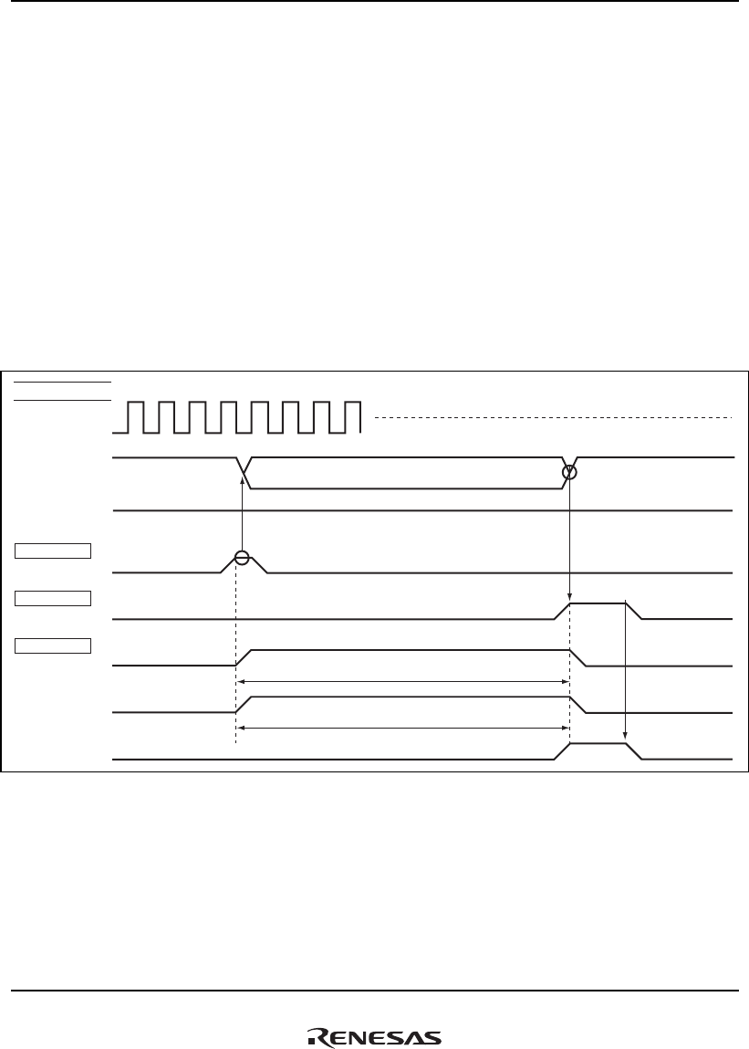
24. Multimedia Card Interface (MMCIF)
Rev.1.00 Jan. 10, 2008 Page 1211 of 1658
REJ09B0261-0100
(3) Operation of Commands Not Requiring Command Response
Some broadcast commands do not require a command response.
Figure 24.3 shows an example of the command sequence for commands that do not require a
command response.
Figure 24.4 shows the operational flow for commands that do not require a command response.
• Make settings to issue the command.
• Set the CMDSTART bit in CMDSTRT to 1 to start command transmission. MMCCMD must
be kept driven until the end bit output is completed.
• The end of the command sequence is detected by poling the BUSY flag in CSTR or by the
command transmit end interrupt (CMDI).
MMCCLK
MMCCMD
MMCDAT
CMDSTRT
(CMDSTART)
INTSTR0
(CMDI)
CSTR
(CWRE)
(BUSY)
(REQ)
Input/output pins
Command output (48 bits)
Command transmission
started Command transmission
ended
Cleared by
software
Command transmission period
Command sequence period
Figure 24.3 Example of Command Sequence for Commands
Not Requiring Command Response
24. Multimedia Card Interface (MMCIF)
Rev.1.00 Jan. 10, 2008 Page 1212 of 1658
REJ09B0261-0100
Ye s
Start of command sequence
Set command data in CMDR0 to CMDR4
Set command type in CMDTYR
Set command response type in RSPTYR
Set the CMDSTART bit in CMDSTRT to 1
(CMDI) interrupt detected?
End of command sequence
No
Figure 24.4 Example of Operational Flow for Commands
Not Requiring Command Response
(4) Operation of Commands without Data Transfer
Broadcast, relative address, and flash memory operation commands include a number of
commands that do not include data transfer. Such commands execute the desired data transfer
using command arguments and command responses. For a command that is related to time-
consuming processing such as flash memory write/erase, the card indicates the data busy state via
the MMCDAT.
Figures 24.5 and 24.6 show examples of the command sequence for commands without data
transfer.
Figure 24.7 shows the operational flow for commands without data transfer.
• Make settings to issue the command.
• Set the CMDSTART bit in CMDSTRT to 1 to start command transmission.
Command transmission completion can be confirmed by the command transmit end interrupt
(CMDI).
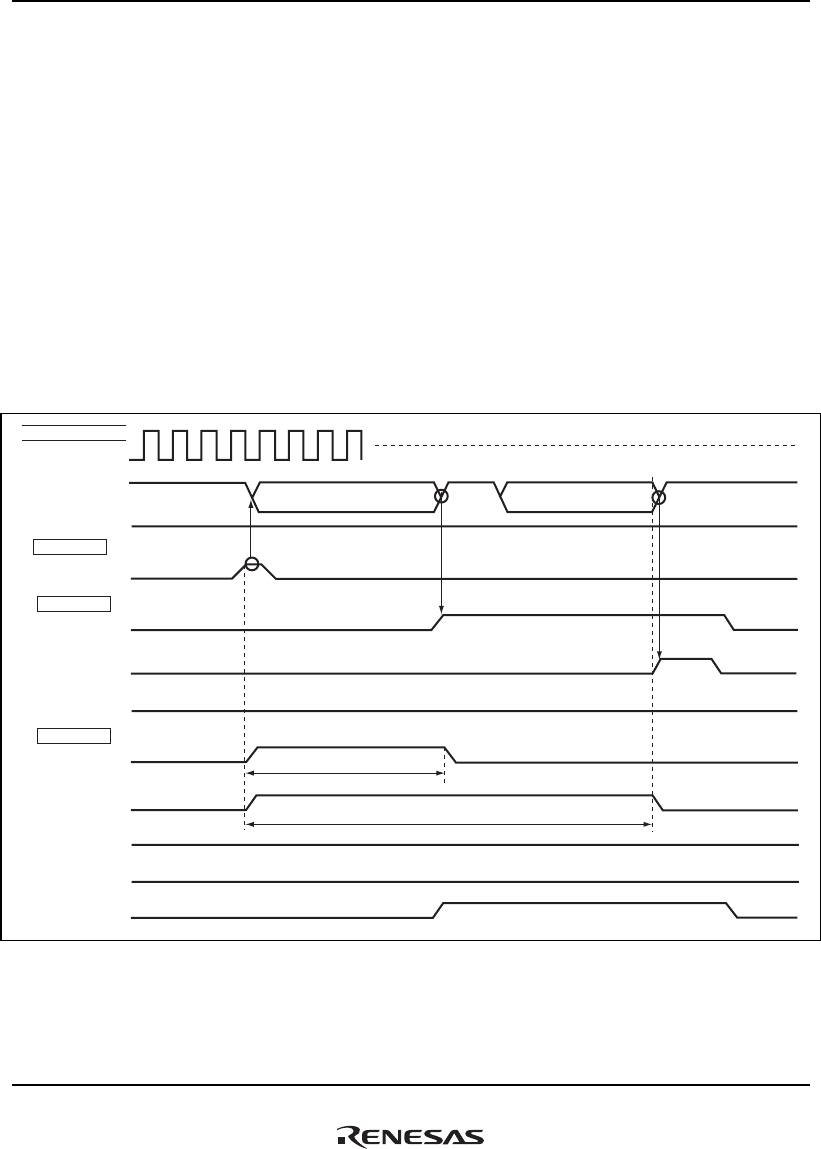
24. Multimedia Card Interface (MMCIF)
Rev.1.00 Jan. 10, 2008 Page 1213 of 1658
REJ09B0261-0100
• The command response is received from the card.
If the card returns no command response, the command response is detected by the command
timeout error (CTERI).
• The end of the command sequence is detected by poling the BUSY flag in CSTR or by the
command response receive end interrupt (CRPI).
• Check whether the state is data busy through the DTBUSY bit in CSTR. If data busy is
detected, the end of the data busy state is then detected through the data busy end interrupt
(DBSYI).
• Write the CMDOFF bit to 1, if a CRC error (CRCERI) or a command timeout error (CTERI)
occurs.
• The MMCCMD and MMCDAT pins go to the high impedance state when the MMCIF and the
MMC card do not drive the bus and the input level of these pins is high because they are
pulled-up internally.
MMCCLK
MMCCMD
MMCDAT
CMDSTRT
(CMDSTART)
INTSTR0
(CMDI)
CSTR
(BUSY)
(CWRE)
(REQ)
(CRPI)
(DBSYI)
(DTBUSY_TU)
(DTBUSY)
Input/output pins
Command output (48 bits)
Command transmission
started
Command response
reception (No busy state)
Command transmission period
Command sequence execution period
Response reception
completed
Figure 24.5 Example of Command Sequence for Commands without Data Transfer
(No Data Busy State)
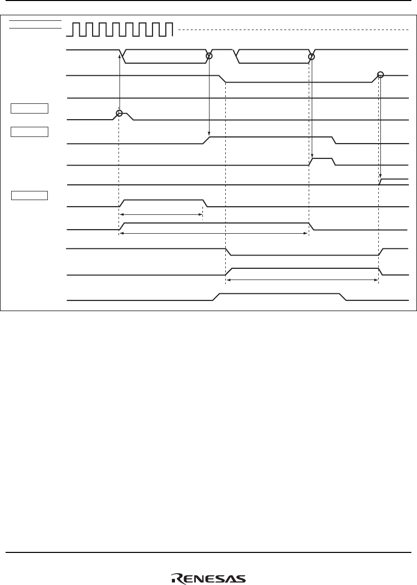
24. Multimedia Card Interface (MMCIF)
Rev.1.00 Jan. 10, 2008 Page 1214 of 1658
REJ09B0261-0100
MMCCLK
MMCCMD
MMCDAT
CMDSTRT
(CMDSTART)
INTSTR0
(CMDI)
CSTR
(CWRE)
(BUSY)
(REQ)
(CRPI)
(DBSYI)
(DTBUSY_TU)
(DTBUSY)
Input/output pins
Command output (48 bits)
Command transmission
started
Command response
reception
Command transmission
period
Command sequence execution period
Response reception
completed
Data busy period
Busy state
ends
(Busy state)
Figure 24.6 Example of Command Sequence for Commands without Data Transfer
(with Data Busy State)
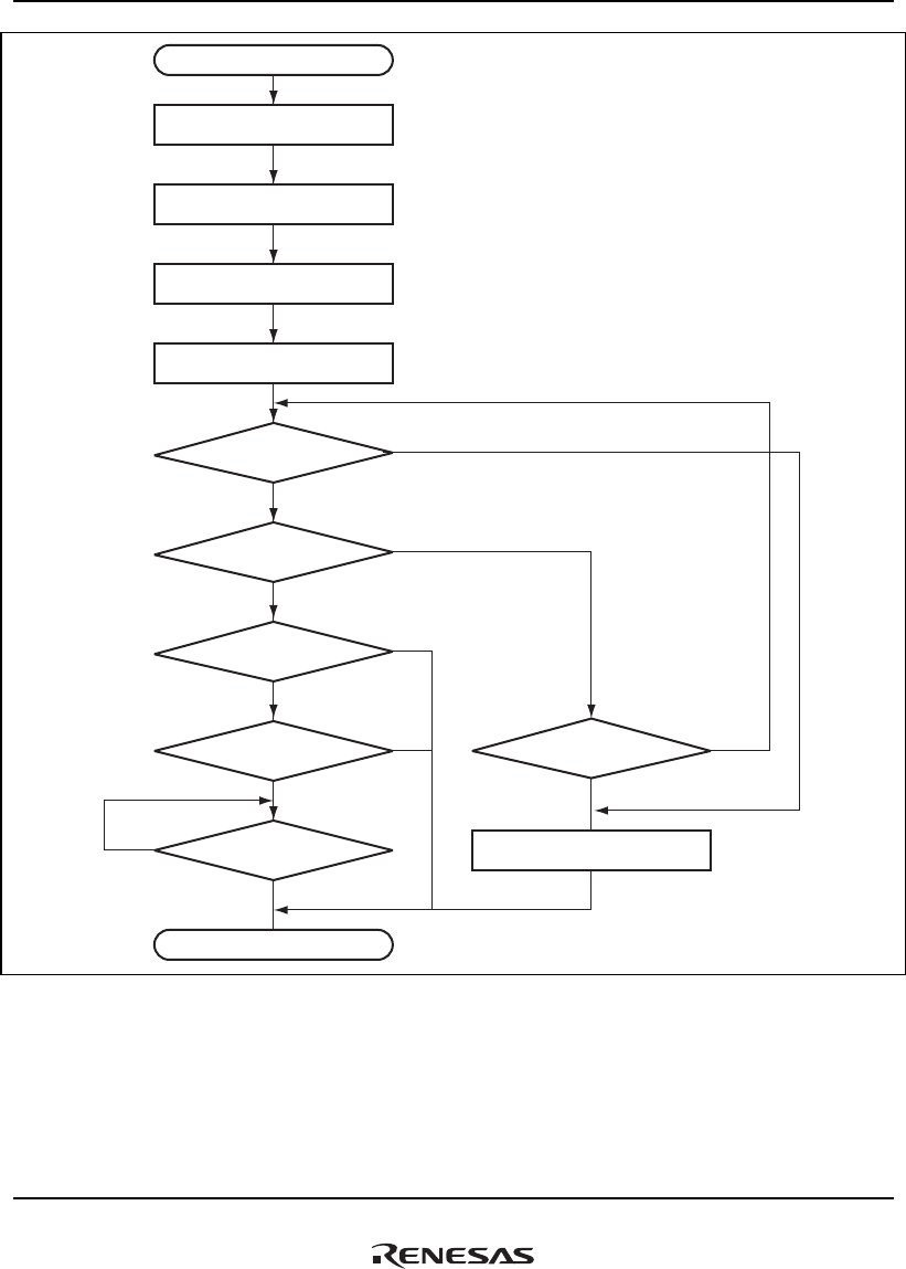
24. Multimedia Card Interface (MMCIF)
Rev.1.00 Jan. 10, 2008 Page 1215 of 1658
REJ09B0261-0100
Start of command sequence
Set command data in
CMDR0 to CMDR4
Set command type in CMDTYR
Set command response type
in RSPTYR
Write 1 to CMDSTRT
Ye s
No
CRCERI
interrupt detected?
Ye s
No
CRPI
interrupt detected?
Ye s
No
R1b
response?
Ye s
No
DTBUSY
detected?
Ye s
No
Ye s
No DBSYI
interrupt detected?
End of command sequence
CTERI interrupt
detected?
Write 1 to CMDOFF
Figure 24.7 Example of Operational Flow for Commands without Data Transfer

24. Multimedia Card Interface (MMCIF)
Rev.1.00 Jan. 10, 2008 Page 1216 of 1658
REJ09B0261-0100
(5) Commands with Read Data
Flash memory operation commands include a number of commands involving read data. Such
commands confirm the card status by the command argument and command response, and receive
card information and flash memory data from the MMCDAT pin.
In multiple block transfer, two transfer methods can be used; one is open-ended and another one is
pre-defined. Open-ended operation is suspended for each block transfer and an instruction to
continue or end the command sequence is waited for. For pre-defined operation, the block number
of the transmission is set before transfer.
When the FIFO is full between blocks in multiple block transfer, the command sequence is
suspended. Once the command sequence is suspended, process the data in FIFO if necessary
before allowing the command sequence to continue.
Note: In multiple block transfer, when the command sequence is ended (the CMDOFF bit is
written to 1) before command response reception (CRPI), the command response may not
be received correctly. Therefore, to receive the command response correctly, the command
sequence must be continued (set the RD_CONT bit to 1) until the command response
reception ends.
Figures 24.8 to 24.11 show examples of the command sequence for commands with read data.
Figures 24.12 to 24.14 show the operational flows for commands with read data.
• Make settings to issue the command, and clear FIFO.
• Set the CMDSTART bit in CMDSTRT to 1 to start command transmission. MMCCMD must
be kept driven until the end bit output is completed.
Command transmission completion can be confirmed by the command transmit end interrupt
(CMDI).
• The command response is received from the card.
If the card does not return the command response, the command response is detected by the
command timeout error (CTERI).
• Read data is received from the card.
• The inter-block suspension in multiple block transfer and suspension by the FIFO full are
detected by the data transfer end interrupt (DTI) and FIFO full interrupt (FFI), respectively.
To continue the command sequence, the RD_CONTI bit in OPCR should be set to 1. To end
the command sequence, the CMDOFF bit in OPCR should be set to 1, and CMD12 should be
issued. Unless the sequence is suspended in pre-defined multiple block transfer, CMD12 is not
needed.
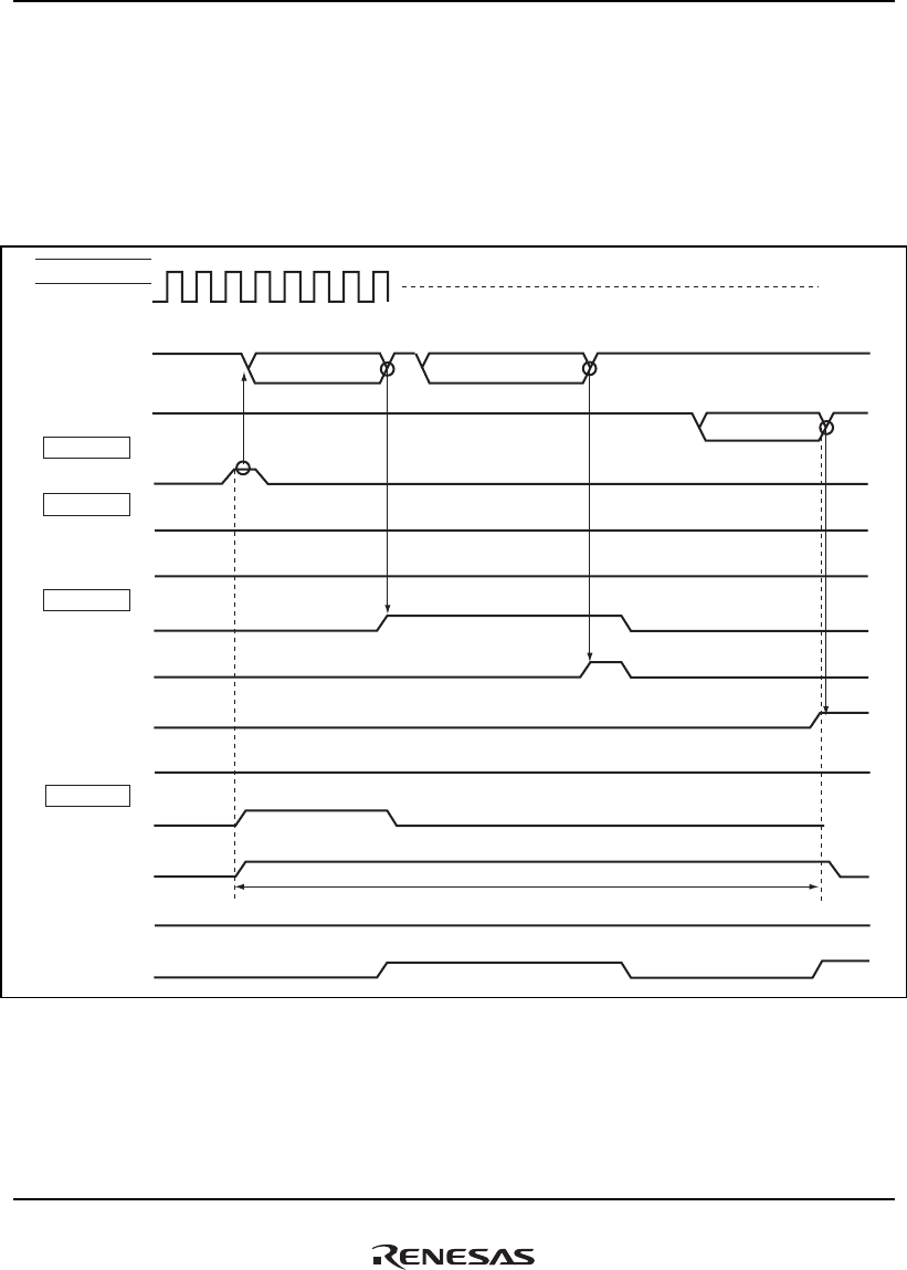
24. Multimedia Card Interface (MMCIF)
Rev.1.00 Jan. 10, 2008 Page 1217 of 1658
REJ09B0261-0100
• The end of the command sequence is detected by poling the BUSY flag in CSTR, by the data
transfer end interrupt (DTI) or pre-defined multiple block transfer end (BTI).
• Write the CMDOFF bit to 1 if a CRC error (CRCERI) or a command timeout error (CTERI)
occurs in the command response reception.
• Clear the FIFO by writing the CMDOFF bit to 1, when CRC error (CRCERI) and data timeout
error (DTERI) occurs in the read data reception.
MMCCLK
MMCCMD
MMCDAT
CMDSTRT
(CMDSTART)
INTSTR0
(CMDI)
(CMDOFF)
CSTR
(CWRE)
(BUSY)
(REQ)
(CRPI)
(DTI)
(FFI)
(FIFO_FULL)
CMD17 (READ_SINGLE_BLOCK)
OPCR
(RD_CONTI)
Input/output pins
Command Command response
Read data
Command
transmission
started
Single block read command execution sequence
Figure 24.8 Example of Command Sequence for Commands with Read Data
(Block Size ≤ FIFO Size)
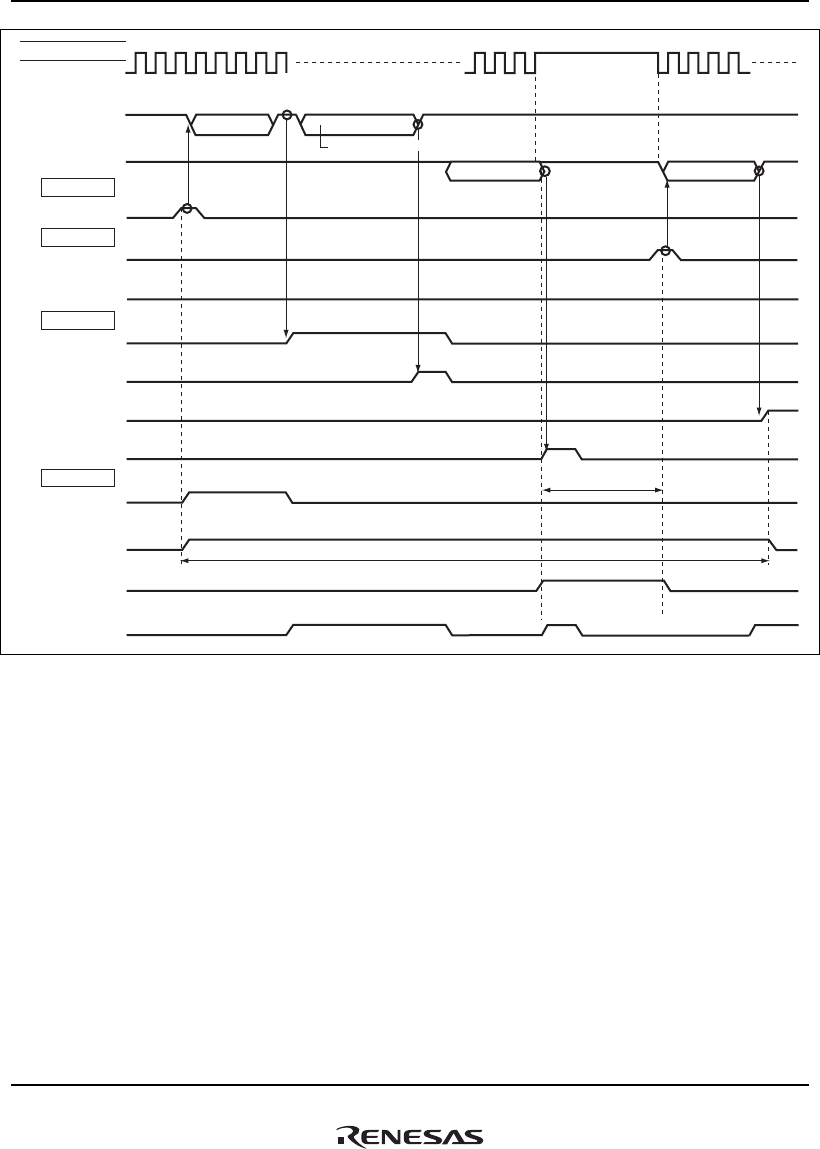
24. Multimedia Card Interface (MMCIF)
Rev.1.00 Jan. 10, 2008 Page 1218 of 1658
REJ09B0261-0100
MMCCLK
MMCCMD
MMCDAT
CMDSTRT
(CMDSTART)
INTSTR0
(CMDI)
(CMDOFF)
CSTR
(CWRE)
(BUSY)
(REQ)
(CRPI)
(DTI)
(FFI)
(FIFO_FULL)
CMD17 (READ_SINGLE_BLOCK)
OPCR
(RD_CONTI)
Input/output pins
Transfer clock
transmission halted
Transfer clock
transmission resumed
Command response
Command
Block data
reception suspended
Read data Read data
Block data
reception resumed
Reading data
from FIFO
Single block read command execution sequence
Command
transmission
started
Figure 24.9 Example of Command Sequence for Commands with Read Data
(Block Size > FIFO Size)
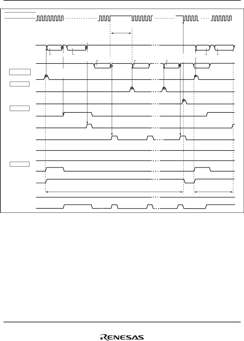
24. Multimedia Card Interface (MMCIF)
Rev.1.00 Jan. 10, 2008 Page 1219 of 1658
REJ09B0261-0100
MMCCLK
MMCCMD
MMCDAT
CMDSTRT
(CMDSTART)
INTSTR0
(CMDI)
(CMDOFF)
CSTR
(CWRE)
(BUSY)
(REQ)
(CRPI)
(DTI)
(FFI)
(BTI)
(FIFO_FULL)
CMD18 (READ_MULTIPLE_BLOCK) CMD12
(STOP_TRANSMISSION)
OPCR
(RD_CONTI)
Input/output pins
Transfer clock
transmission halted
Transfer clock
transmission resumed
Read data
Block data
reception ended
Multiblock read command execution sequence
Stop command
execution sequence
Command Command
Command
transmission started
Command
response
Read data Read data
Command
response
Figure 24.10 Example of Command Sequence for Commands with Read Data
(Multiple Block Transfer)
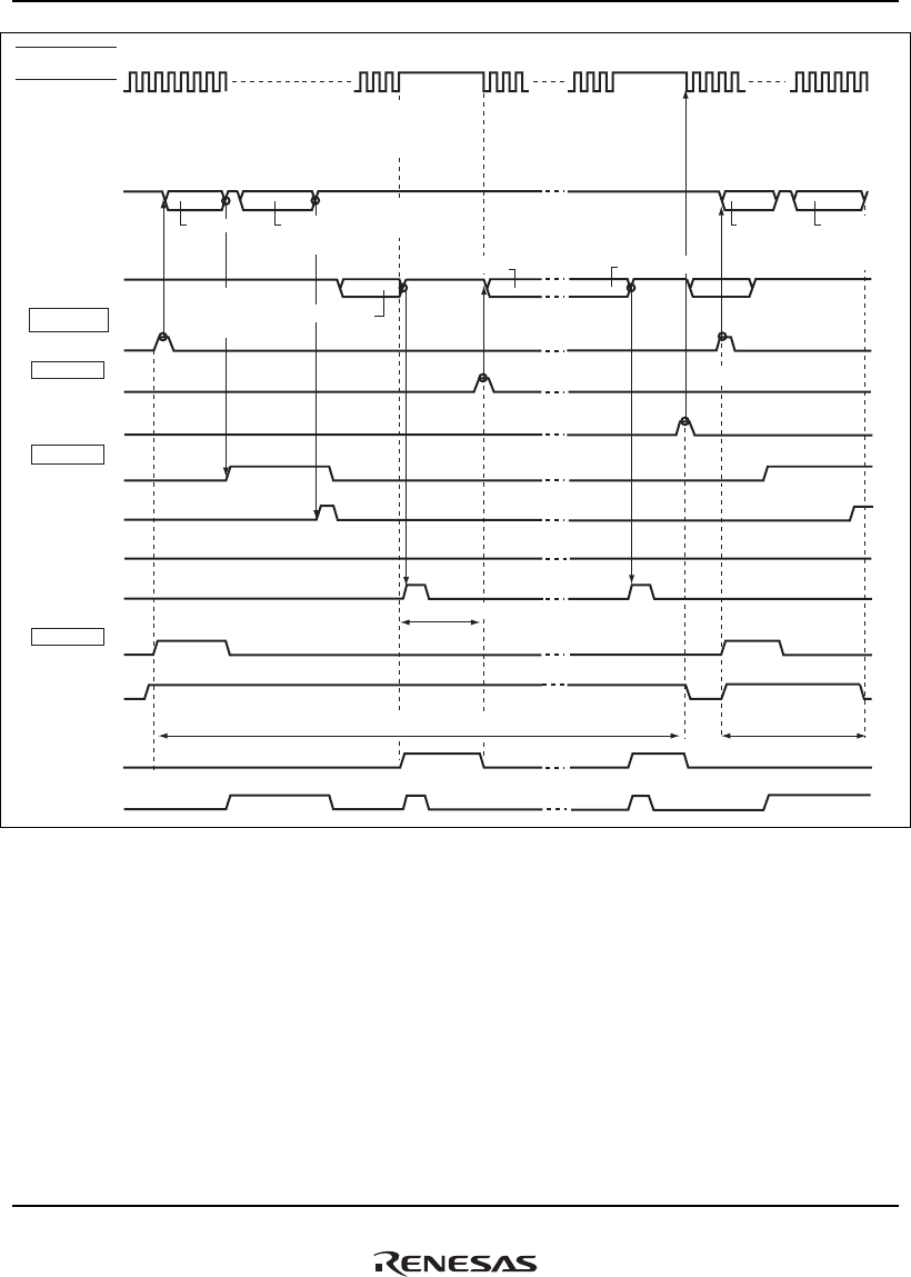
24. Multimedia Card Interface (MMCIF)
Rev.1.00 Jan. 10, 2008 Page 1220 of 1658
REJ09B0261-0100
CMD11 (READ_DAT_UNTIL_STOP)
CMD12
(STOP_TRANSMISSION)
Input/output
pins
Transfer clock
transmission resumed
Transfer clock
transmission resumed
Stop command
execution sequence
Data reception
resumed
Data reception ended
Read data from FIFO
Stream read command execution sequence
MMCCLK
MMCCMD
MMCDAT
CMDSTRT
(CMDSTART)
INTSTR0
(CMDI)
(CMDOFF)
CSTR
(CWRE)
(BUSY)
(REQ)
(CRPI)
(DTI)
(FFI)
(FIFO_FULL)
OPCR
(RD_CONTI)
Command
Read data
Read data
Read data
Command
response
Command Command
response
Command
transmission
started
Transfer clock
transmission
halted
Data reception
suspended
Figure 24.11 Example of Command Sequence for Commands with Read Data
(Stream Transfer)
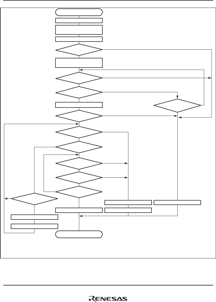
24. Multimedia Card Interface (MMCIF)
Rev.1.00 Jan. 10, 2008 Page 1221 of 1658
REJ09B0261-0100
Start of command sequence
Clear FIFO
Execute CMD16
Read response register
Execute CMD17
(Set CMDR then CMDSTRT)
Set the size of block
for transfer in TBCR
No
Ye s
CRCERI interrupt
detected?
Ye s
No
CMD16
normal end?
Ye s
No
CRPI inte rrupt
detected?
Ye s
No
Response status
normal?
Ye s
No
End of command sequence
CTERI interrupt
detected?
Ye s
No FFI interrupt
detected? Set CMDOFF to 1
Read data from FIFO
Set RD_CONTI to 1
Read data from FIFO
No
Ye s
DTERI interrupt
detected?
No
Ye s
CRCERI interrupt
detected?
No
Ye s
Legend:
Len: Block length [bytes]
Cap: FIFO size [bytes]
n (FFI): Number of FIFO full interrupts (FFI) from the start of read sequence
DTERI interrupt
detected?
Ye s
No DTI interrupt
detected?
Ye s
No Cap ≥
Len - Cap × n (FFI)
Set CMDOFF to 1
Clear FIFO
Figure 24.12 Example of Operational Flow for Commands with Read Data
(Single Block Transfer)
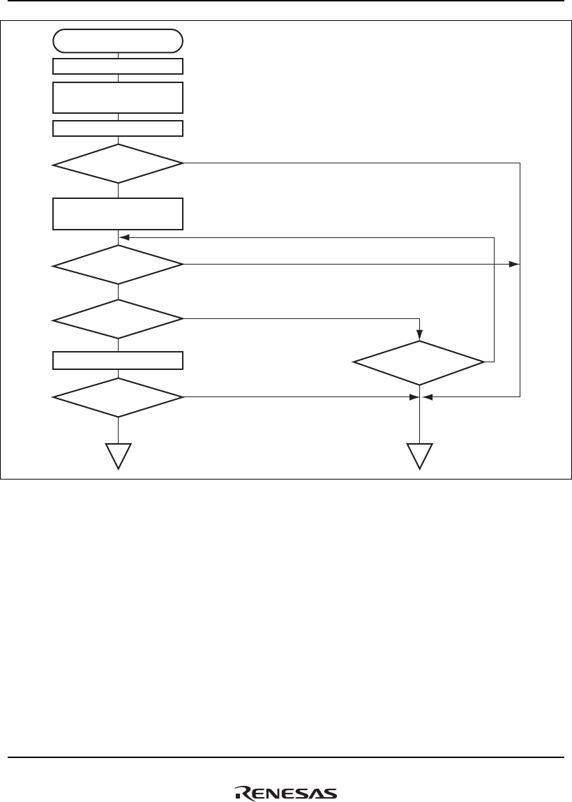
24. Multimedia Card Interface (MMCIF)
Rev.1.00 Jan. 10, 2008 Page 1222 of 1658
REJ09B0261-0100
Start of command sequence
Clear FIFO
Execute CMD16
Read response register
Execute CMD18
(Set CMDR then CMDSTRT)
Set the block size in TBCR
No
Ye s
CRCERI interrupt
detected?
Ye s
No
CMD16
normal end?
Ye s
No
CRPI interrupt
detected?
Ye s
No
Response status
normal?
Ye s
No
CTERI interrupt
detected?
12
Figure 24.13 Example of Operational Flow for Commands with Read Data (1)
(Open-ended Multiple Block Transfer)
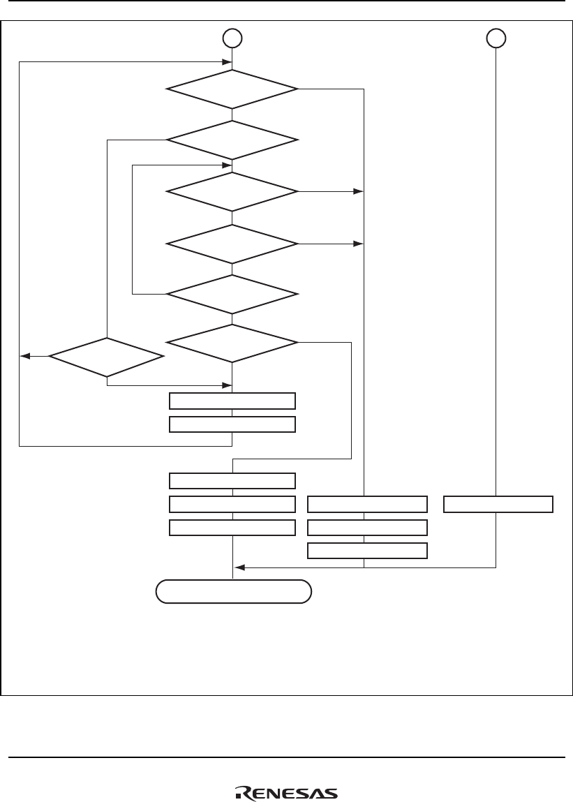
24. Multimedia Card Interface (MMCIF)
Rev.1.00 Jan. 10, 2008 Page 1223 of 1658
REJ09B0261-0100
End of command sequence
Ye s
No FFI interrupt
detected?
Set CMDOFF to 1
Read data from FIFO
Set RD_CONTI to 1
Read data from FIFO
No
Ye s
DTERI interrupt
detected?
No
Ye s
CRCERI interrupt
detected?
No
Ye s
Legend:
Len: Block length [bytes]
Cap: FIFO size [bytes]
n (FFI): Number of FIFO full interrupts (FFI) from the start of read sequence
n (DTI): Number of data transfer end interrupts (DTI) from the start of read sequence
DTERI interrupt
detected?
Ye s
No
Read next block?
Ye s
No DTI interrupt
detected?
Ye s
No Cap ≥
Len (1 + n (DTI))
- Cap × n (FFI)
Set CMDOFF to 1
Execute CMD12
Set CMDOFF to 1
Execute CMD12
Clear FIFO
1 2
Figure 24.13 Example of Operational Flow for Commands with Read Data (2)
(Open-ended Multiple Block Transfer)
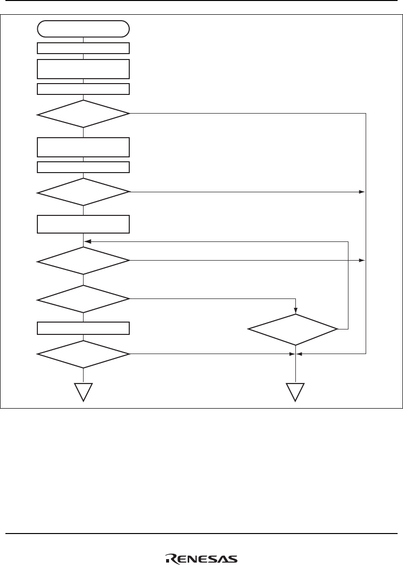
24. Multimedia Card Interface (MMCIF)
Rev.1.00 Jan. 10, 2008 Page 1224 of 1658
REJ09B0261-0100
Start of command sequence
Clear FIFO
Execute CMD16
Read response register
Execute CMD18
(Set CMDR then CMDSTRT)
Set the block size in TBCR
No
Ye s
CRCERI interrupt
detected?
Ye s
No
CMD16
normal end?
Execute CMD23
Set the number of blocks
for transfer (TBNCR)
Ye s
No
CMD23
normal end?
Ye s
No
CRPI interrupt
detected?
Ye s
No
Response status
normal?
Ye s
No
CTERI interrupt
detected?
12
Figure 24.13 Example of Operational Flow for Commands with Read Data (3)
(Pre-defined Multiple Block Transfer)
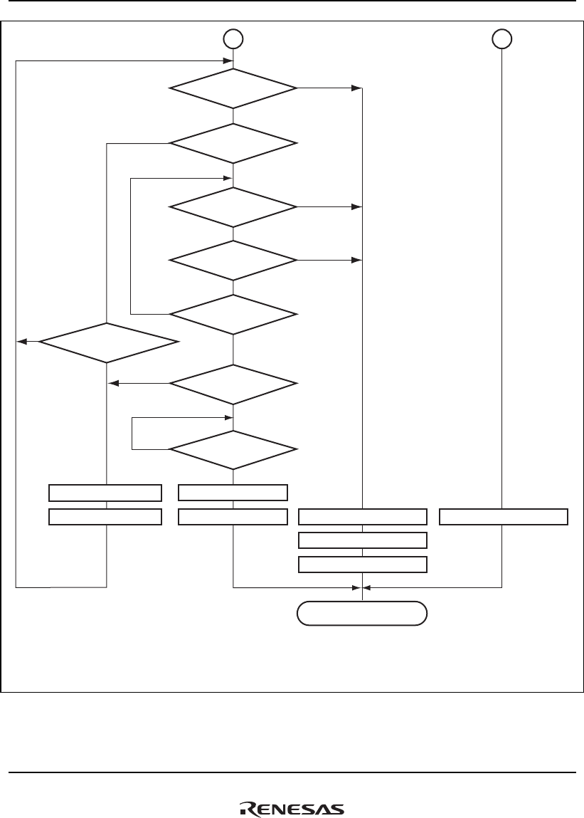
24. Multimedia Card Interface (MMCIF)
Rev.1.00 Jan. 10, 2008 Page 1225 of 1658
REJ09B0261-0100
End of command sequence
Ye s
No FFI interrupt
detected?
Set CMDOFF to 1
Read data from FIFO
Set RD_CONTI to 1
No
Ye s
DTERI interrupt
detected?
No
Ye s
CRCERI interrupt
detected?
No
Ye s
Legend:
Len: Block length [bytes]
Cap: FIFO size [bytes]
n (FFI): Number of FIFO full interrupts (FFI) from the start of read sequence
n (DTI): Number of data transfer end interrupts (DTI) from the start of read sequence
DTERI interrupt
detected?
Ye s
No BTI interrupt
detected?
Ye s
No DTI interrupt
detected?
Ye s
No
Cap ≥
Len (1 + n (DTI))
- Cap × n (FFI)
Ye s
No
TBNCR value
= n (DTI) ?
Set CMDOFF to 1
Execute CMD12
Read data from FIFO
Set CMDOFF to 1
Clear FIFO
1 2
Figure 24.13 Example of Operational Flow for Commands with Read Data (4)
(Pre-defined Multiple Block Transfer)
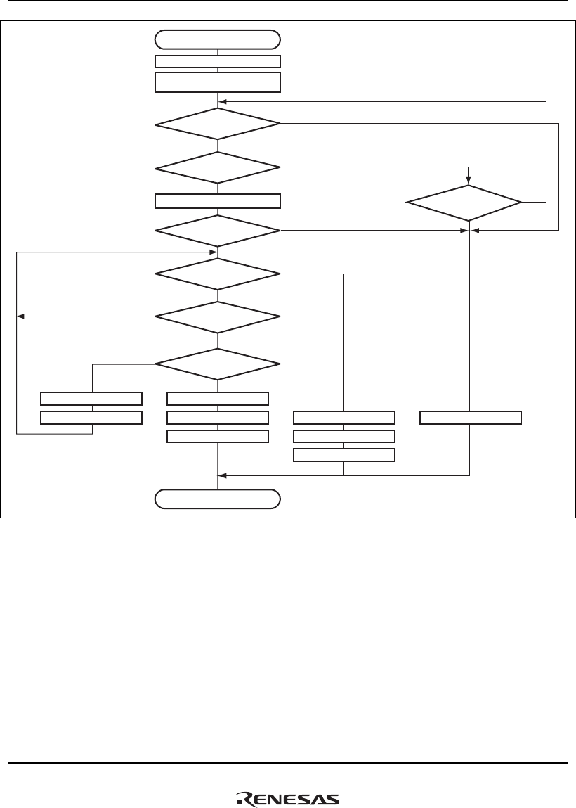
24. Multimedia Card Interface (MMCIF)
Rev.1.00 Jan. 10, 2008 Page 1226 of 1658
REJ09B0261-0100
Start of command sequence
Clear FIFO
Read response register
Execute CMD11
(CMDR to CMDSTRT)
No
Ye s
(CRCERI) interrupt
detected?
Ye s
No
(CRPI) interrupt
detected?
Ye s
No
Response status
normal ended?
Ye s
No
End of command sequence
(CTERI) interrupt
detected?
Ye s
No (FFI) interrupt
detected?
Set the CMDOFF to 1
Read data from FIFO
Set the RD_CONTI to 1
No
Ye s
(DTERI) interrupt
detected?
Ye s
No Data read
completed?
Set the CMDOFF to 1
Execute CMD12Execute CMD12
Read data from FIFO
Set the CMDOFF to 1
Clear FIFO
Figure 24.14 Example of Operational Flow for Commands with Read Data
(Stream Transfer)

24. Multimedia Card Interface (MMCIF)
Rev.1.00 Jan. 10, 2008 Page 1227 of 1658
REJ09B0261-0100
(6) Commands with Write Data
Flash memory operation commands include a number of commands involving write data. Such
commands confirm the card status by the command argument and command response, and
transmit card information and flash memory data via the MMCDAT pin. For a command that is
related to time-consuming processing such as flash memory write, the card indicates the data busy
state via the MMCDAT pin.
In multiple block transfer, two transfer methods can be used; one is open-ended and the other is
pre-defined. Open-ended operation is suspended for each block transfer and an instruction to
continue or end the command sequence is waited for. For pre-defined operation, the block number
of the transmission is set before transfer.
When the FIFO is full between blocks in multiple block transfer, the command sequence is
suspended. Once the command sequence is suspended, process the data in FIFO if necessary
before allowing the command sequence to continue.
Figures 24.15 to 24.18 show examples of the command sequence for commands with write data.
Figures 24.19 to 24.21 show the operational flows for commands with write data.
• Make settings to issue a command, and clear FIFO.
• Set the CMDSTART bit in CMDSTRT to 1 to start command transmission. MMCCMD must
be kept driven until the end bit output is completed.
• Command transmission completion can be confirmed by the command transmit end interrupt
(CMDI).
• The command response is received from the card.
• If the card returns no command response, the command response is detected by the command
timeout error (CTERI).
• Set the write data to FIFO.
• Set the DATAEN bit in OPCR to 1 to start write data transmission. MMCDAT must be kept
driven until the end bit output is completed.
• Inter-block suspension in multiple block transfer and suspension according to the FIFO empty
are detected by the data response interrupt (DRPI) and FIFO empty interrupt (FEI),
respectively. To continue the command sequence, set the next data to FIFO and set the
DATAEN bit in OPCR to 1. To end the command sequence, set the CMDOFF bit in OPCR to
1 and issue CMD12. Unless the sequence is suspended in pre-defined multiple block transfer,
CMD12 is not needed.

24. Multimedia Card Interface (MMCIF)
Rev.1.00 Jan. 10, 2008 Page 1228 of 1658
REJ09B0261-0100
• The end of the command sequence is detected by poling the BUSY flag in CSTR, data transfer
end interrupt (DTI), data response interrupt (DRPI), or pre-defined multiple block transfer end
(BTI).
• The data busy state is checked through DTBUSY in CSTR. If the card is in data busy state, the
end of the data busy state is detected by the data busy end interrupt (DBSYI).
• Write the CMDOFF bit to 1 if a CRC error (CRCERI) or a command timeout error (CTERI)
occurs in the command response reception.
• Write the CMDOFF bit to 1 if a CRC error (CRCERI) or a data timeout error (DTERI) occurs
in the write data transmission.
Note: In a write to the card by stream transfer, the MMCIF continues data transfer to the card
even after a FIFO empty interrupt is detected. In this case, complete the command
sequence after at least 24 transfer clock cycles.
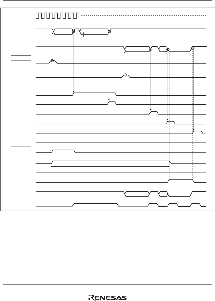
24. Multimedia Card Interface (MMCIF)
Rev.1.00 Jan. 10, 2008 Page 1229 of 1658
REJ09B0261-0100
MMCCLK
MMCCMD
MMCDAT
CMDSTRT
(CMDSTART)
(CMDI)
CSTR
(CWRE)
(BUSY)
(DTBUSY)
(DTBUSY_TU)
(REQ)
(CRPI)
(DTI)
(DBSYI)
(FEI)
(FIFO_EMPTY)
CMD24 (WRITE_SINGLE_BLOCK)
OPCR
(DATAEN)
(DRPI)
INTSTR0
Input/output pins
Command
Command
response
Command
transmission
started
Single block write command execution sequence
Write data
Status
Busy
Figure 24.15 Example of Command Sequence for Commands with Write Data
(Block Size ≤ FIFO Size)
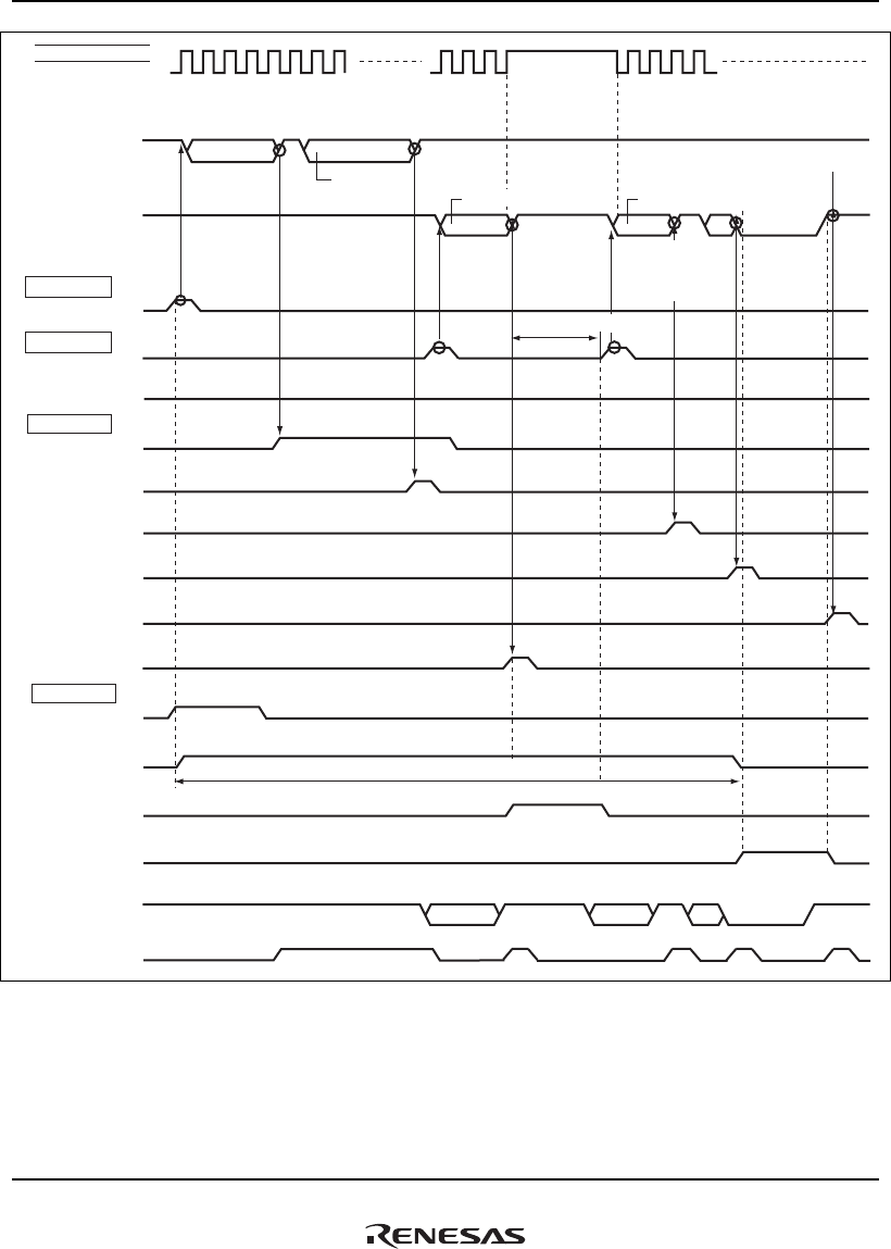
24. Multimedia Card Interface (MMCIF)
Rev.1.00 Jan. 10, 2008 Page 1230 of 1658
REJ09B0261-0100
MMCCLK
MMCCMD
MMCDAT
CMDSTRT
(CMDSTART)
INTSTR0
(CMDI)
(CMDOFF)
CSTR
(CWRE)
(BUSY)
(DTBUSY)
(DTBUSY_TU)
(REQ)
(CRPI)
(DRPI)
(DBSYI)
(DTI)
(FEI)
(FIFO_EMPTY)
CMD24 (WRITE_SINGLE_BLOCK)
OPCR
(DATAEN)
Input/output pins
Command
Command
response
Command
transmission
started
Busy
Transfer clock
transmission
halted
Transfer clock
transmission resumed
Block data
transmission
suspended
Writing data to FIFO
Write data Write data
Block data
transmission
resumed
Single block write command execution sequence
Figure 24.16 Example of Command Sequence for Commands with Write Data
(Block Size > FIFO Size)
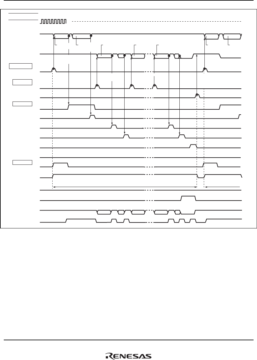
24. Multimedia Card Interface (MMCIF)
Rev.1.00 Jan. 10, 2008 Page 1231 of 1658
REJ09B0261-0100
MMCCLK
MMCCMD
MMCDAT
CMDSTRT
(CMDSTART)
INTSTR0
(CMDI)
(CMDOFF)
CSTR
(CWRE)
(BUSY)
(DTBUSY)
(DTBUSY_TU)
(REQ)
(CRPI)
(DRPI)
(DBSYI)
(DTI)
(FEI)
(FIFO_EMPTY)
CMD25 (WRITE_MULTIPE_BLOCK) CMD12(STOP_TRANSMISSION)
OPCR
(DATAEN)
Input/output pins
Write data Write data Write data
Status Status
Block data
transmission
started
Block data
reception
ended
Next block data
transmission
started
Stop-command
execution sequence
Command Command
response Command Command
response
Command
transmission
started
Figure 24.17 Example of Command Sequence for Commands with Write Data
(Multiple Block Transfer)
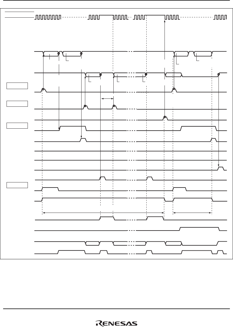
24. Multimedia Card Interface (MMCIF)
Rev.1.00 Jan. 10, 2008 Page 1232 of 1658
REJ09B0261-0100
MMCCLK
MMCCMD
MMCDAT
CMDSTRT
(CMDSTART)
INTSTR0
(CMDI)
(CMDOFF)
CSTR
(CWRE)
(BUSY)
(DTBUSY)
(DTBUSY_TU)
(REQ)
(CRPI)
(DRPI)
(DBSYI)
(DTI)
(FEI)
(FIFO_EMPTY)
CMD20 (WRITE_DAT_UNTIL_STOP) CMD12(STOP_TRANSMISSION)
OPCR
(DATAEN)
Input/output pins
Command Command
response Command
Stop command
execution sequence
Busy
Transfer
clock
trans-
mission
halted
Transfer
clock
trans-
mission
halted
Transfer
clock
transmission
resumed
Transfer
clock
transmission
resumed
Writing data to FIFO
Data
transmission
suspended
Data
transmission
suspended
Data
transmission
resumed
Data
transmission
ended
Stream write command execution sequence
Command
response
Command
transmission
started
Write data Write data Write data
Figure 24.18 Example of Command Sequence for Commands with Write Data
(Stream Transfer)
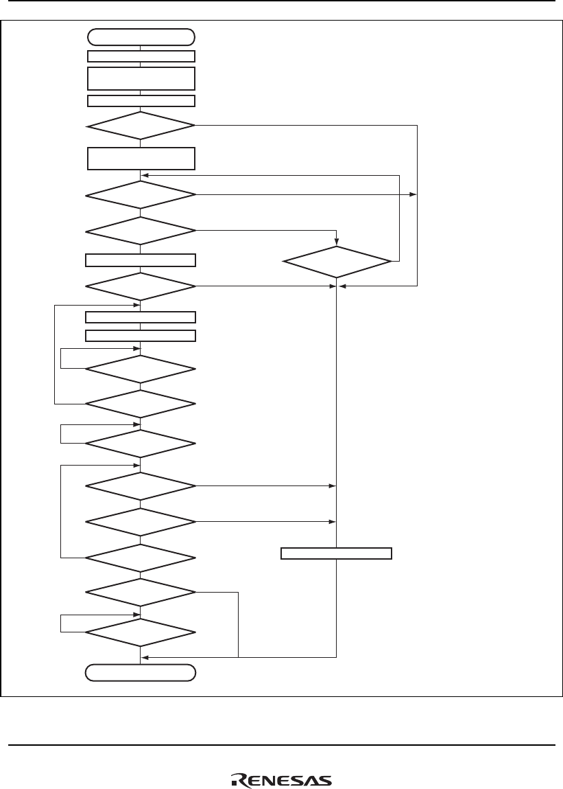
24. Multimedia Card Interface (MMCIF)
Rev.1.00 Jan. 10, 2008 Page 1233 of 1658
REJ09B0261-0100
Start of command sequence
Clear FIFO
Execute CMD16
Read response register
Execute CMD24
(Set CMDR then CMDSTRT)
Set the size of block
for transfer in TBCR
No
Ye s
CRCERI interrupt
detected?
Ye s
No
CMD16
normal end?
Ye s
No
CRPI interrupt
detected?
Ye s
No
No
Response status
normal?
Ye s
No
End of command sequence
CTERI interrupt
detected?
Set CMDOFF to 1
Write data to FIFO
Set DATAEN to 1
Ye s
DTBUSY detected?
Ye s
DBSYI interrupt
detected?
No
Ye s
CRCERI interrupt
detected?
No
Ye s
Legend:
Len: Block length [bytes]
Cap: FIFO size [bytes]
n (FEI): Number of FIFO empty interrupts (FEI)
from the start of read sequence
DTERI interrupt
detected?
Ye s
No DRPI interrupt
detected?
Ye s
Cap × n (FEI) ≥ Len
No
No
Ye s
DTI interrupt
detected?
No
Ye s
FEI interrupt
detected?
No
Figure 24.19 Example of Operational Flow for Commands with Write Data
(Single Block Transfer)
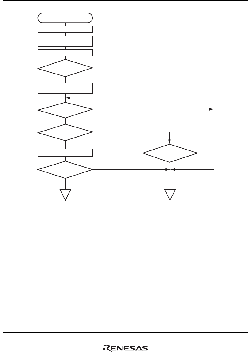
24. Multimedia Card Interface (MMCIF)
Rev.1.00 Jan. 10, 2008 Page 1234 of 1658
REJ09B0261-0100
Start of command sequence
Clear FIFO
Execute CMD16
Read response register
Execute CMD25
(Set CMDR then CMDSTRT)
Set the block size in TBCR
No
Ye s
CRCERI interrupt
detected?
Ye s
No
CMD16
normal end?
Ye s
No
CRPI interrupt
detected?
Ye s
No
Response status
normal?
Ye s
No
CTERI interrupt
detected?
12
Figure 24.20 (1) Example of Operational Flow for Commands with Write Data
(Open-ended Multiple Block Transfer)
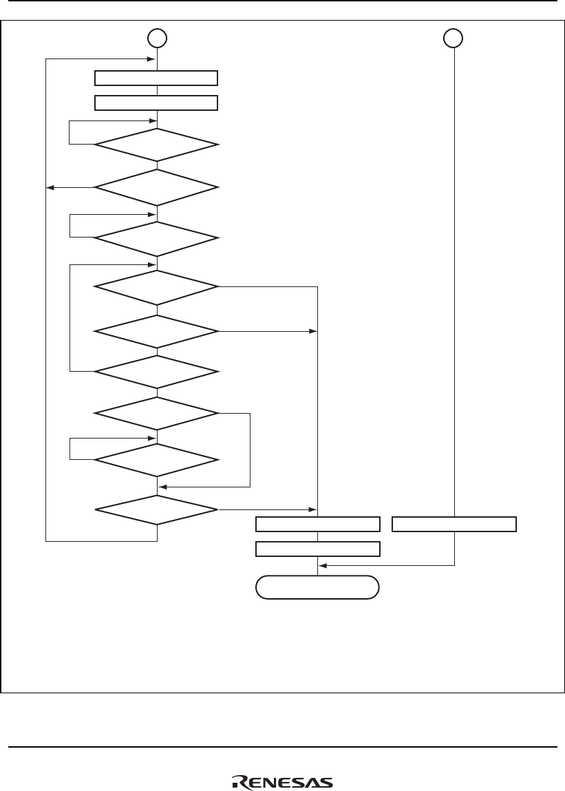
24. Multimedia Card Interface (MMCIF)
Rev.1.00 Jan. 10, 2008 Page 1235 of 1658
REJ09B0261-0100
No
End of command sequence
Write data to FIFO
Set DATAEN to 1
Ye s
No
Next block write?
Ye s
DTBUSY detected?
Ye s
DBSYI interrupt
detected?
No
Ye s
*
CRCERI interrupt
detected?
No
Ye s
Note: * Write block size of data (if block size < or = FIFO size) or FIFO size of data (if block size > FIFO size).
Len: Block length [bytes]
Cap: FIFO size [bytes]
n (FEI): Number of FIFO empty interrupts (FEI) from the start of read sequence
n (DRPI): Number of data response interrupts (DRPI) from the start of write sequence
Legend:
DTERI interrupt
detected?
Ye s
No DRPI interrupt
detected?
Ye s
Cap × n (FEI)
- Len (1 + n (DTI))
≥ Len
No
No
Ye s
DTI interrupt
detected?
No
Ye s
FEI interrupt
detected?
No
Set CMDOFF to 1Set CMDOFF to 1
Execute CMD12
1 2
Figure 24.20 (2) Example of Operational Flow for Commands with Write Data
(Open-ended Multiple Block Transfer)
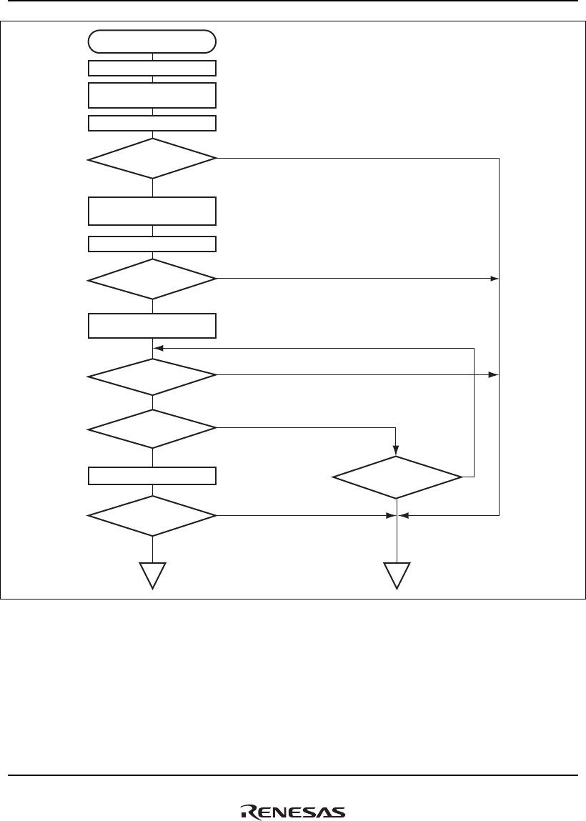
24. Multimedia Card Interface (MMCIF)
Rev.1.00 Jan. 10, 2008 Page 1236 of 1658
REJ09B0261-0100
Start of command sequence
Clear FIFO
Execute CMD16
Set the number of
blocks in TBNCR
Read response register
Execute CMD25
(Set CMDR then CMDSTRT)
Set the block size in TBCR
No
Ye s
CRCERI interrupt
detected?
Ye s
No
CMD16
normal end?
Ye s
No
CRPI interrupt
detected?
Ye s
No
Response status
normal?
Ye s
No
CTERI interrupt
detected?
Execute CMD 23
Ye s
No
CMD 23
normal end?
12
Figure 24.20 (3) Example of Operational Flow for Commands with Write Data
(Pre-defined Multiple Block Transfer)
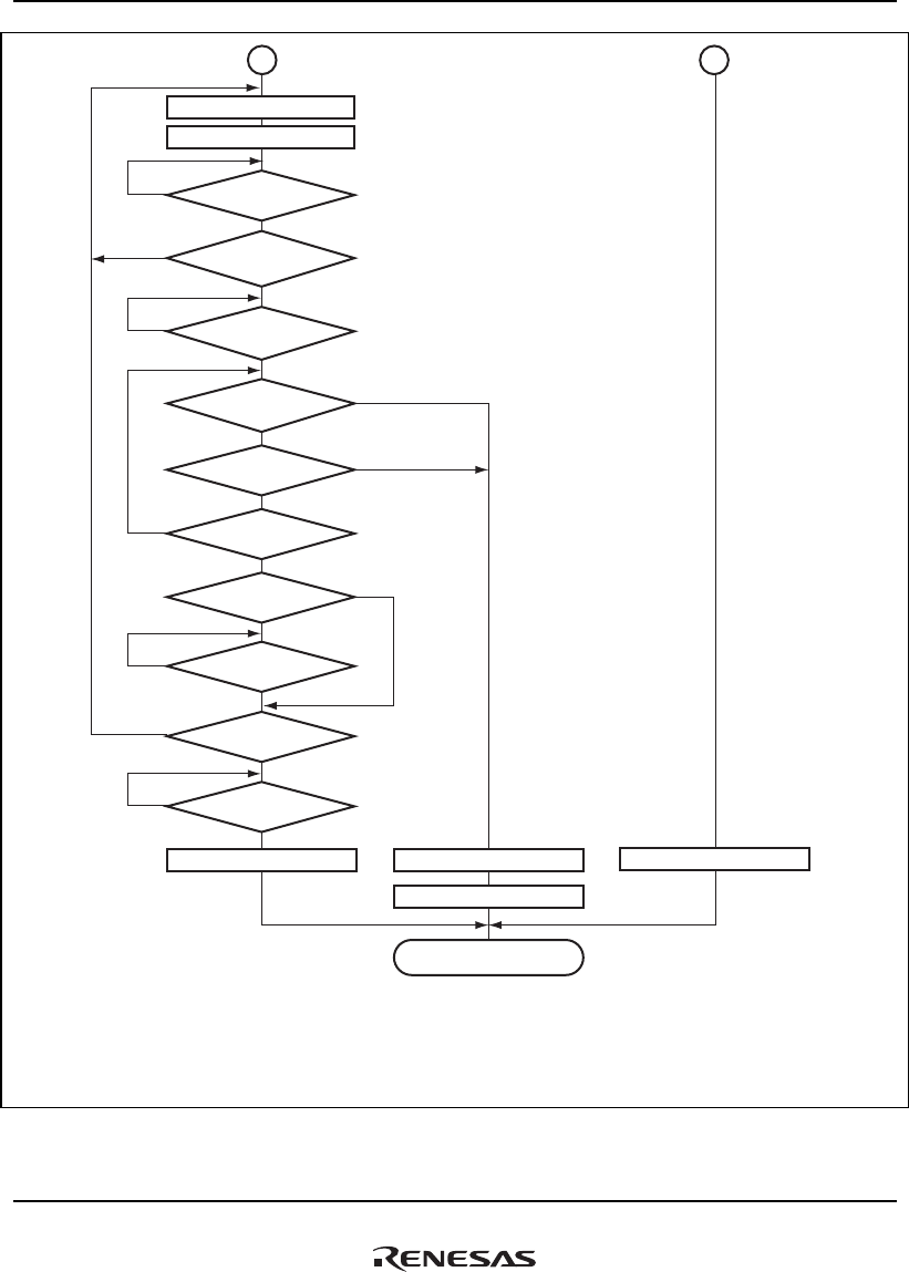
24. Multimedia Card Interface (MMCIF)
Rev.1.00 Jan. 10, 2008 Page 1237 of 1658
REJ09B0261-0100
No
End of command sequence
Write data to FIFO
Set DATAEN to 1
Ye s
DTBUSY detected?
Ye s
DBSYI interrupt
detected?
No
Ye s
*
CRCERI interrupt
detected?
No
Ye s
Note: * Write block size of data (if block size < or = FIFO size) or FIFO size of data (if block size > FIFO size).
Len: Block length [bytes]
Cap: FIFO size [bytes]
n (FEI): Number of FIFO empty interrupts (FEI) from the start of read sequence
n (DRPI): Number of data response interrupts (DRPI) from the start of write sequence
Legend:
DTERI interrupt
detected?
Ye s
No DRPI interrupt
detected?
Ye s
Cap × n (FEI)
- Len (1 + n (DRPI))
≥ Len
No
No
Ye s
TBNCR = n(DRPI)?
No
Ye s
BTI interrupt
detected?
No
Ye s
DTI interrupt
detected?
No
Ye s
FEI interrupt
detected?
No
Set CMDOFF to 1Set CMDOFF to 1
Execute CMD12
1 2
Set CMDOFF to 1
Figure 24.20 (4) Example of Operational Flow for Commands with Write Data
(Pre-defined Multiple Block Transfer)
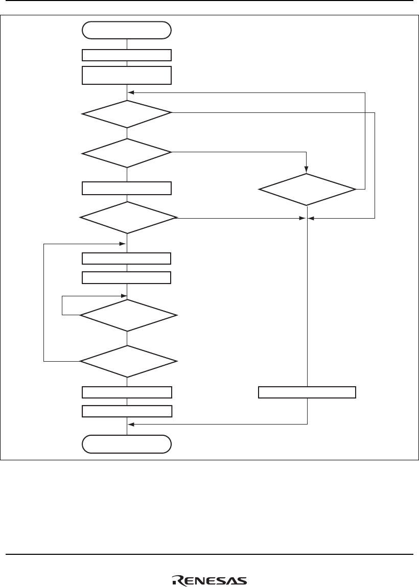
24. Multimedia Card Interface (MMCIF)
Rev.1.00 Jan. 10, 2008 Page 1238 of 1658
REJ09B0261-0100
Start of command sequence
Clear FIFO
Read response register
Execute CMD20
(Set CMDR then CMDSTRT)
No
Ye s
CRCERI interrupt
detected?
Ye s
No
CRPI interrupt
detected?
Ye s
No
Response status
normal?
Ye s
No
CTERI interrupt
detected?
End of command sequence
Write data to FIFO
Set DATAEN to 1
Ye s
No All data written
to FIFO?
Ye s
FEI interrupt
detected?
No
Set CMDOFF to 1Set CMDOFF to 1
Execute CMD12
Figure 24.21 Example of Operational Flow for Commands with Write Data
(Stream Transfer)

24. Multimedia Card Interface (MMCIF)
Rev.1.00 Jan. 10, 2008 Page 1239 of 1658
REJ09B0261-0100
24.5 MMCIF Interrupt Sources
Table 24.7 lists the MMCIF interrupt sources. The interrupt sources are classified into four groups,
and four interrupt vectors are assigned. Each interrupt source can be individually enabled by the
enable bits in INTCR0 to INTCR2. Disabled interrupt sources do not set the flag.
Table 24.7 MMCIF Interrupt Sources
Name Interrupt source Interrupt flag
FIFO empty FEI FSTAT
FIFO full FFI
Data response DRPI
Data transfer end DTI
Command response receive end CRPI
Command transmit end CMDI
TRAN
Data busy end DBSYI
CRC error CRCERI
Data timeout error DTERI
ERR
Command timeout error CTERI
FRDY FIFO ready FRDYI

24. Multimedia Card Interface (MMCIF)
Rev.1.00 Jan. 10, 2008 Page 1240 of 1658
REJ09B0261-0100
24.6 Operations when Using DMA
24.6.1 Operation in Read Sequence
In order to transfer data in FIFO with the DMAC, set MMCIF (DMACR) after setting the
DMAC*. Transmit the read command after setting DMACR.
Figure 24.22 to 24.24 shows the operational flow for a read sequence.
• Clear FIFO and make settings in DMACR.
• Read command transmission is started.
• Command response is received from the card.
• Read data is received from the card.
• After the read sequence, data remains in FIFO. If necessary, write 100 to SET[2:0] in DMACR
to read all data from FIFO.
• Confirm that the DMAC transfer is completed and set the DMAEN bit in DMACR to 0.
• Set the CMDOFF bit to 1 and clear DMACR to H'00 if a CRC error (CRCERI) or a command
timeout error (CTERI) occurs in the command response reception.
• Set the CMDOFF bit to 1, clear DMACR to H'00, and clear FIFO if a CRC error (CRCERI) or
a data timeout error (DTERI) occurs in the read data reception.
When using DMA, next block read is resumed automatically when the AUTO bit in DMACR is
set to 1 and normal read is detected after the block transfer end of a pre-defined multiple block
transfer. Figure 24.25 shows the operational flow for a pre-defined multiple block read using auto-
mode.
• Clear FIFO.
• Set the block number to (TBNCR).
• Set DMACR.
• Read command transmission is started.
• Command response is received from the card.
• Read data is received from the card.
• Detect the command timeout error (CTERI) if a command response is not received from the
card.
• The end of the command sequence is detected by poling the BUSY flag in CSTR or through
the pre-defined multiple block transfer end flag (BTI).

24. Multimedia Card Interface (MMCIF)
Rev.1.00 Jan. 10, 2008 Page 1241 of 1658
REJ09B0261-0100
• An error in a command sequence (during data reception) is detected through the CRC error
flag or data timeout flag. When these flags are detected, set the CMDOFF bit in OPCR to 1,
issue CMD12 and suspend the command sequence.
• The data remains in FIFO after the read sequence end. Set the SET[2:0] bits in DMACR to 100
to read all data in FIFO if necessary.
• Confirm the DMA transfer end and clear the DMAEN bit in DMACR to 0.
• Set the CMDOFF bit to 1 and clear DMACR to H'00 if a CRC error (CRCERI) or a command
timeout error (CTERI) occurs in the command response reception.
• Set the CMDOFF bit to 1, clear DMACR to H'00, and clear FIFO if a CRC error (CRCERI) or
a data timeout error (DTERI) occurs in the read data reception.
Notes: 1. In multiple block transfer, when the command sequence is ended (the CMDOFF bit is
written to 1) before command response reception (CRPI), the command response may
not be received correctly. Therefore, to receive the command response correctly, the
command sequence must be continued (set the RD_CONT bit to 1) until the command
response reception ends.
2. Access from the DMAC to FIFO must be done in bytes or words.
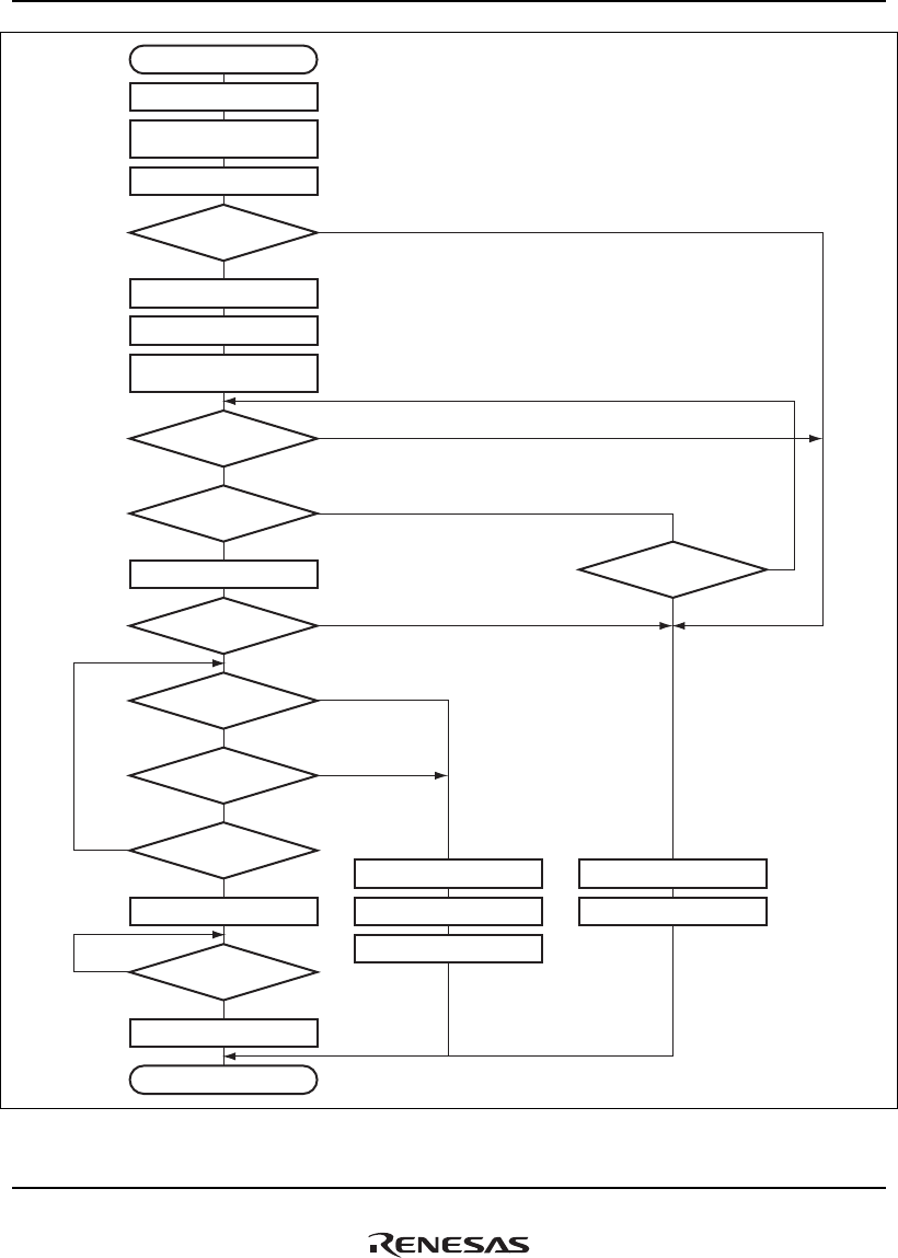
24. Multimedia Card Interface (MMCIF)
Rev.1.00 Jan. 10, 2008 Page 1242 of 1658
REJ09B0261-0100
Start of command sequence
End of command sequence
Clear FIFO
Execute CMD16
Configure the DMAC
Set DMACR (in the MMCIF)
Read response register
Set DMACR to H'84 Clear DMACR to H'00
Set CMDOFF to 1
Clear DMACR to H'00
CMD16
normal end?
No
Ye s
CRPI interrupt
detected?
No
Ye s
Response status
normal?
No
Ye s
DTI interrupt
detected?
No
Ye s
DMA transfer end?
No
Ye s
CTERI interrupt
detected?
No
Ye s
CRCERI interrupt
detected?
Ye s
No
CRCERI interrupt
detected?
Ye s
No
DTERI interrupt
detected?
Ye s
No
Set the size of block
for transfer in TBCR
Execute CMD17
(Set CMDR then CMDSTRT)
Set CMDOFF to 1
Clear DMACR to H'00
Clear FIFO
Figure 24.22 Example of Read Sequence Flow (Single Block Transfer)
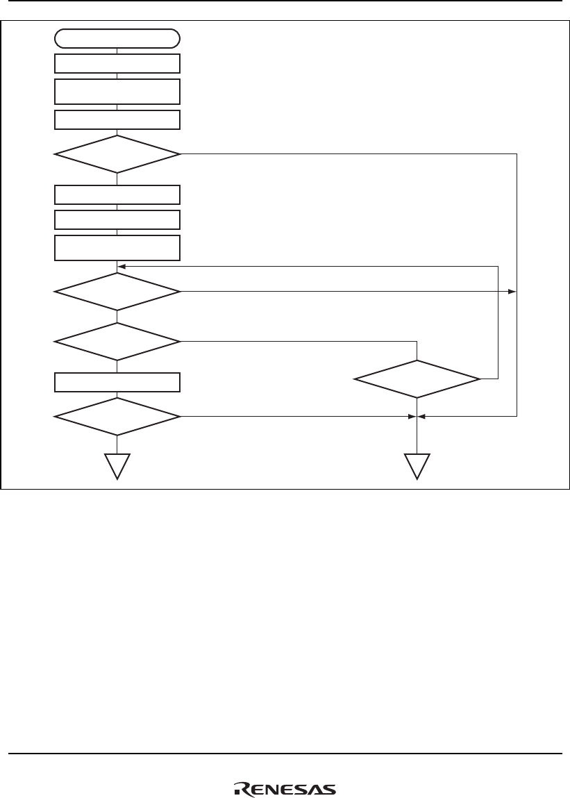
24. Multimedia Card Interface (MMCIF)
Rev.1.00 Jan. 10, 2008 Page 1243 of 1658
REJ09B0261-0100
Start of command sequence
Clear FIFO
Execute CMD16
Configure the DMAC
Set DMACR (in the MMCIF)
Read response register
CMD16
normal end?
No
Ye s
CRPI interrupt
detected?
No
Ye s
Response status
normal?
No
Ye s
CTERI interrupt
detected?
No
Ye s
CRCERI interrupt
detected?
Ye s
No
Set the block size in TBCR
Execute CMD 18
(Set CMDR then CMDSTRT)
1 2
Figure 24.23 (1) Example of Read Sequence Flow (Open-ended Multiple Block Transfer)
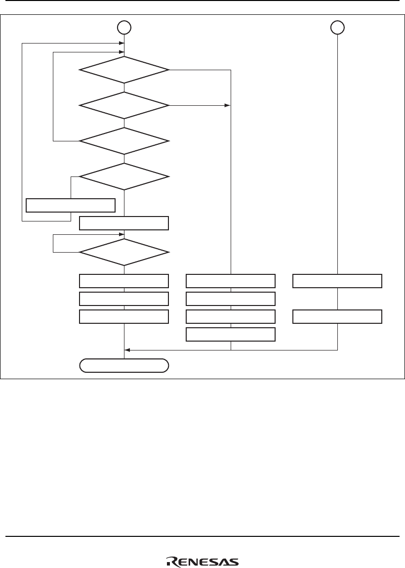
24. Multimedia Card Interface (MMCIF)
Rev.1.00 Jan. 10, 2008 Page 1244 of 1658
REJ09B0261-0100
End of command sequence
Set DMACR to H'84
Clear DMACR to H'00
Set CMDOFF to 1
Clear DMACR to H'00
Execute CMD12
Set CMDOFF to 1
DTI interrupt
detected?
No
Ye s
DMA transfer end?
No
Ye s
CRCERI interrupt
detected?
Ye s
No
DTERI interrupt
detected?
Ye s
No
Next block read?
No
Ye s
12
Set RD_CONTI to 1
Set CMDOFF to 1
Clear DMACR to H'00
Clear FIFO
Execute CMD12
Figure 24.23 (2) Example of Read Sequence Flow (Open-ended Multiple Block Transfer)
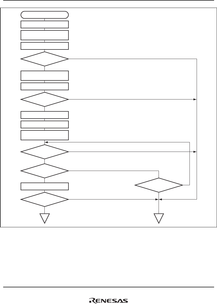
24. Multimedia Card Interface (MMCIF)
Rev.1.00 Jan. 10, 2008 Page 1245 of 1658
REJ09B0261-0100
Start of command sequence
Clear FIFO
Execute CMD16
Configure the DMAC
Set DMACR (in the MMCIF)
Read response register
CMD16
normal end?
No
Ye s
CRPI interrupt
detected?
No
Ye s
Response status
normal?
No
Ye s
CTERI interrupt
detected?
No
Ye s
CRCERI interrupt
detected?
Ye s
No
Set the block size in TBCR
Set the number of
blocks in TBNCR
Execute CMD 18
(Set CMDR then CMDSTRT)
Execute CMD 23
CMD 23
normal end?
No
Ye s
1 2
Figure 24.23 (3) Example of Read Sequence Flow (Pre-defined Multiple Block Transfer)
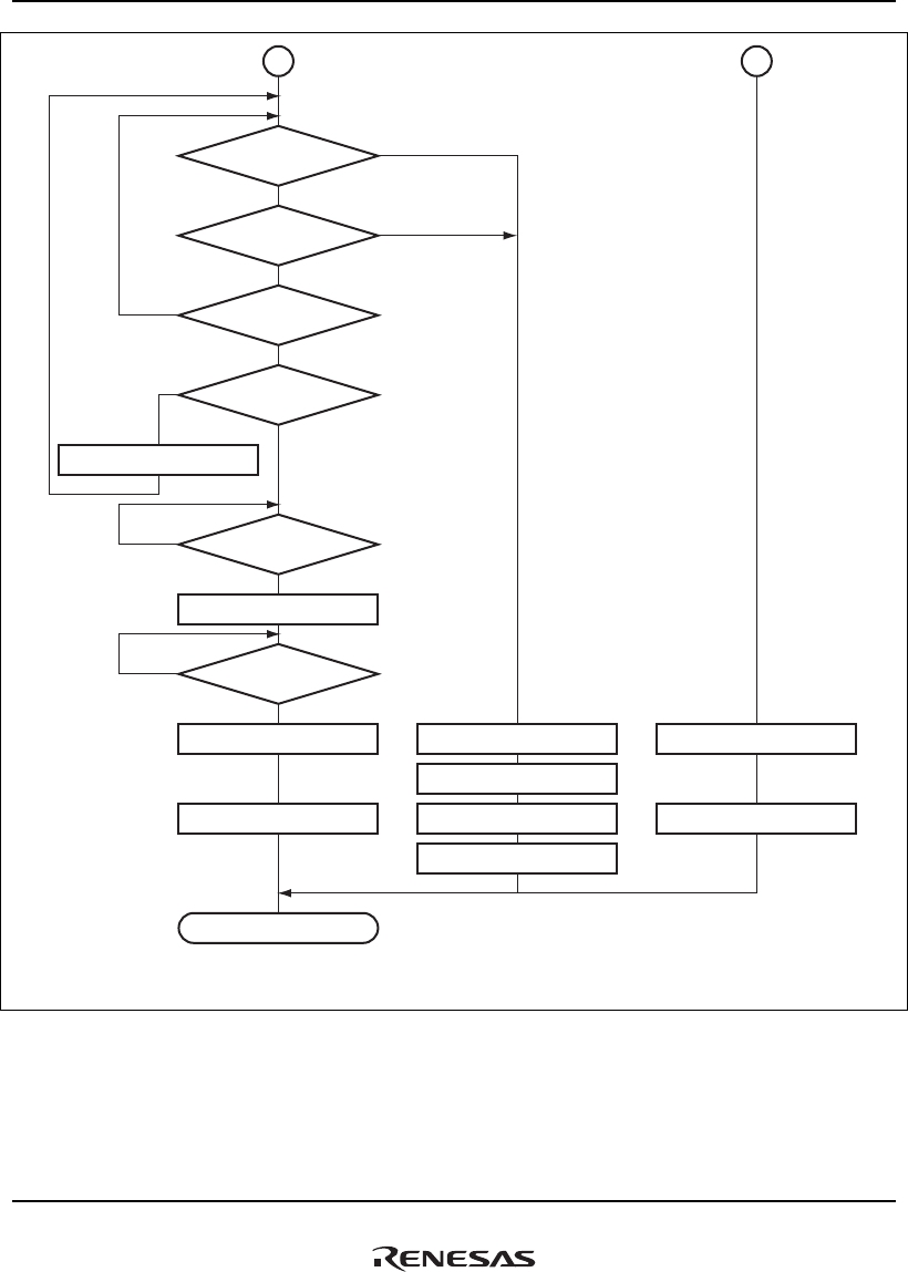
24. Multimedia Card Interface (MMCIF)
Rev.1.00 Jan. 10, 2008 Page 1246 of 1658
REJ09B0261-0100
End of command sequence
Set DMACR to H'84
Clear DMACR to H'00
Set CMDOFF to 1
Clear DMACR to H'00
Set CMDOFF to 1
DTI interrupt
detected?
No
Ye s
DMA transfer end?
No
Ye s
CRCERI interrupt
detected?
Ye s
No
DTERI interrupt
detected?
Ye s
No
BTI interrupt
detected?
No
Ye s
TBNCR = n (DTI)?
No
Ye s
Legend:
n (DTI): Number of data transfer end interrupts (DTI) from the start of read sequence
1 2
Set RD_CONTI to 1
Set CMDOFF to 1
Clear DMACR to H'00
Clear FIFO
Execute CMD12
Figure 24.23 (4) Example of Read Sequence Flow (Pre-defined Multiple Block Transfer)
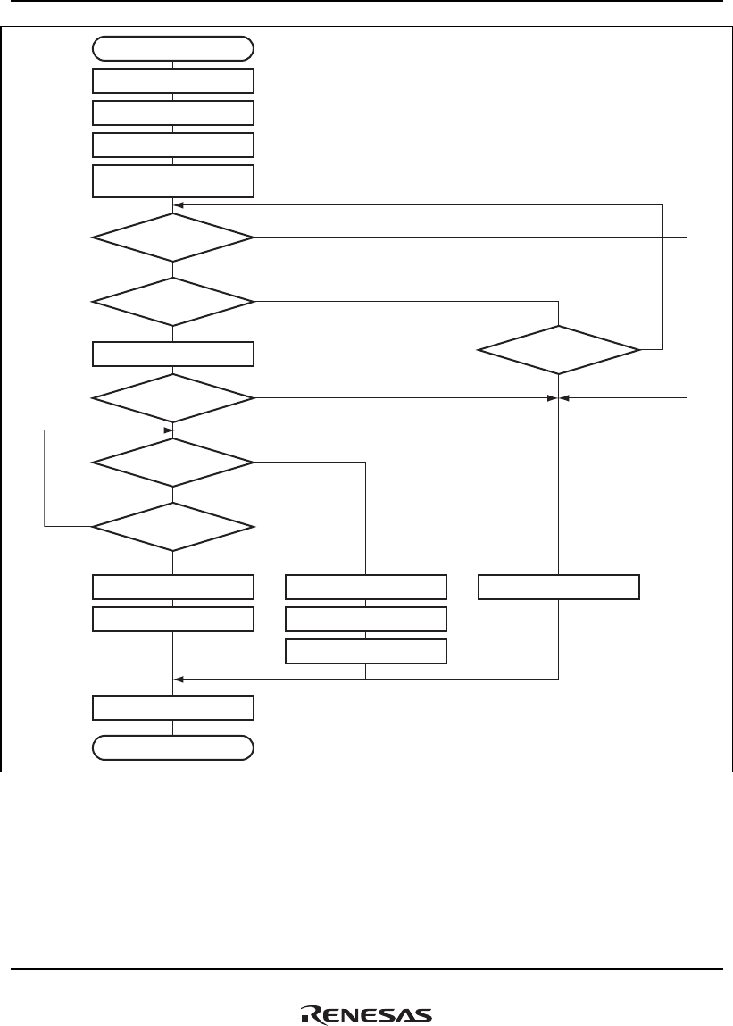
24. Multimedia Card Interface (MMCIF)
Rev.1.00 Jan. 10, 2008 Page 1247 of 1658
REJ09B0261-0100
Start of command sequence
End of command sequence
Clear FIFO
Configure the DMAC
Set DMACR (in the MMCIF)
Read response register
Set CMDOFF to 1
Execute CMD12
Set CMDOFF to 1
Clear DMACR to H'00
CRPI interrupt
detected?
No
Ye s
Response status
normal?
No
Ye s
DMA transfer end?
No
Ye s
CTERI interrupt
detected?
No
Ye s
CRCERI interrupt
detected?
Ye s
No
DTERI interrupt
detected?
Ye s
No
Execute CMD11
(Set CMDR then CMDSTRT)
Set CMDOFF to 1
Execute CMD12
Clear FIFO
Figure 24.24 Example of Operational Flow for Stream Read Transfer

24. Multimedia Card Interface (MMCIF)
Rev.1.00 Jan. 10, 2008 Page 1248 of 1658
REJ09B0261-0100
Start of command sequence
Clear FIFO
Execute CMD16
Configure the DMAC
Set DMACR (in the MMCIF)
(Specify auto mode)
Read response register
CMD16
normal end?
No
Ye s
CRPI interrupt
detected?
No
Ye s
Response status
normal?
No
Ye s
CTERI interrupt
detected?
No
Ye s
CRCERI interrupt
detected?
Ye s
No
Set the block size in TBCR
Set the number of blocks
for transfer in TBNCR
Execute CMD 18
(Set CMDR then CMDSTRT)
Execute CMD 23
CMD 23
normal end?
No
Ye s
1 2
Figure 24.25 (1) Example of Operational Flow for Auto-mode
Pre-defined Multiple Block Read Transfer
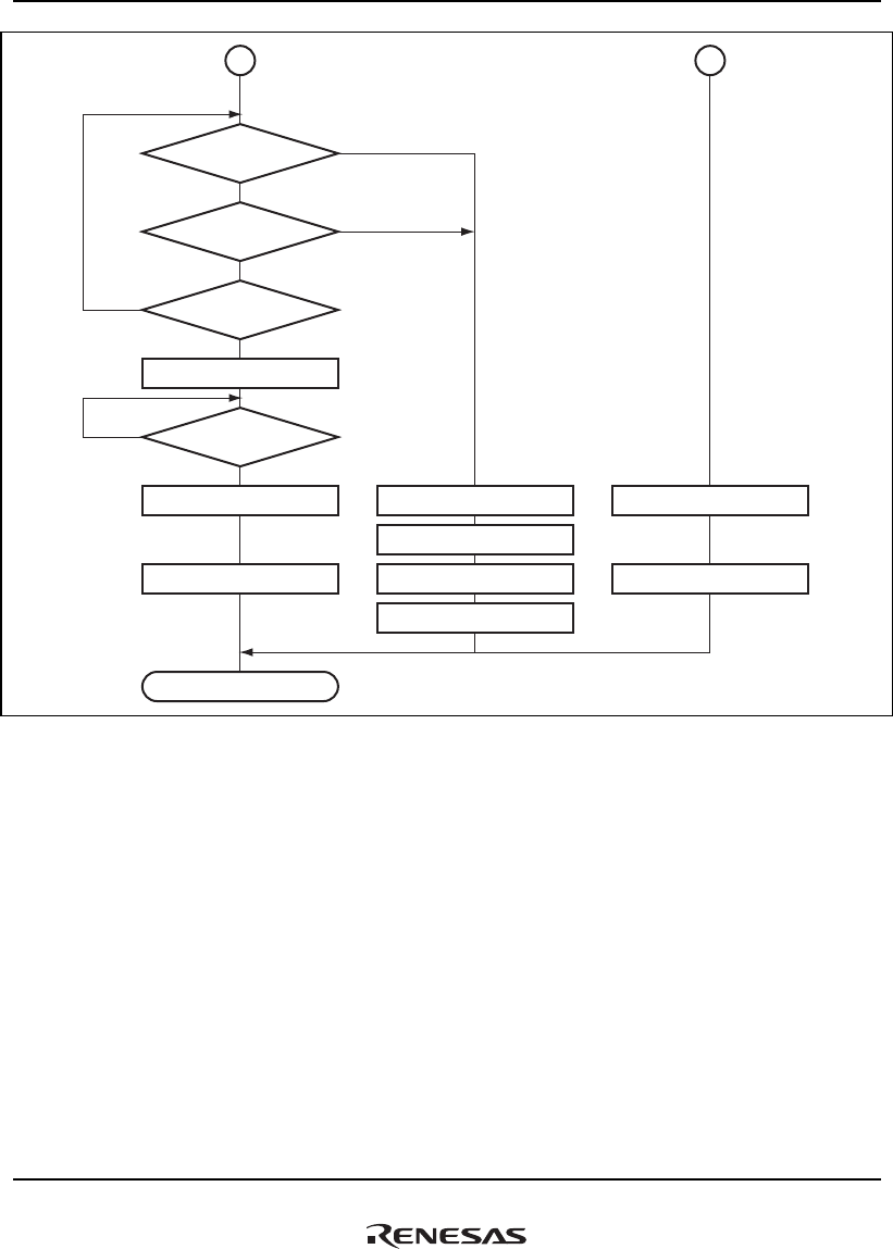
24. Multimedia Card Interface (MMCIF)
Rev.1.00 Jan. 10, 2008 Page 1249 of 1658
REJ09B0261-0100
End of command sequence
Set DMACR to H'84
Set CMDOFF to 1
Clear DMACR to H'00 Clear DMACR to H'00
Clear FIFO
Execute CMD12
Set CMDOFF to 1
Clear DMACR to H'00
Set CMDOFF to 1
BTI interrupt
detected?
No
Ye s
DMA transfer end?
No
Ye s
CRCERI interrupt
detected?
Ye s
No
DTERI interrupt
detected?
Ye s
No
1 2
Figure 24.25 (2) Example of Operational Flow for Auto-mode
Pre-defined Multiple Block Read Transfer

24. Multimedia Card Interface (MMCIF)
Rev.1.00 Jan. 10, 2008 Page 1250 of 1658
REJ09B0261-0100
24.6.2 Operation in Write Sequence
To transfer data to FIFO with the DMAC, set MMCIF (DMACR) after setting the DMAC. Then,
start transfer to the card after a FIFO ready interrupt. Figure 24.26 to 24.28 shows the operational
flow for a write sequence.
• Clear FIFO.
• Transmit write command.
• Make settings in DMACR, and set write data to FIFO.
• Check whether data exceeding the DMACR setting condition is written to FIFO by a FIFO
ready interrupt (FRDYI) or DMAC has transferred all data to FIFO. Then set 1 to the
DATAEN bit in OPCR to start write-data transmission.
In a write to the card by stream transfer, the MMCIF continues data transfer to the card even
after a FIFO empty interrupt is detected. Therefore, complete the write sequence after at least
24 card clock cycles.
• Confirm that the DMAC transfer is completed and be sure to clear the DMAEN bit in
DMACR to 0.
• Set the CMDOFF bit to 1 if a CRC error (CRCERI) or a data timeout error (DTERI) occurs in
the command response reception.
• Set the CMDOFF bit to 1, clear FIFO, and clear DMACR to H'00 if a CRC error (CRCERI) or
a data timeout error (DTERI) occurs in the write data transmission.
When using DMA, an inter-block interrupt can be processed by hardware in pre-defined multiple
block transfer by setting the AUTO bit in DMACR to 1. Figure 24.29 shows the operational flow
for a pre-defined multiple block write sequence using auto-mode.
• Clear FIFO.
• Set the block number to TBNCR.
• Set the CMDSTART bit in CMDSTRT to 1 and begin command transmission.
• Command response is received from the card.
• A command timeout error (CTERI) is detected if a command response is not received from the
card.
• Set DMACR and write data in FIFO.
• Confirm that the DMA transfer has been completed and clear the DMAEN bit in DMACR to
0.
• Detect the end of the command sequence by poling the BUSY flag in CSTR or through the
pre-defined multiple block transfer end flag (BTI).

24. Multimedia Card Interface (MMCIF)
Rev.1.00 Jan. 10, 2008 Page 1251 of 1658
REJ09B0261-0100
• An error in a command sequence (during data transmission) is detected through the CRC error
flag (CRCERI) or data timeout error flag. When these flags are detected, set the CMDOFF bit
in OPCR to 1, issue CMD12 (Stop Tran in SPI mode), and suspend the command sequence.
• Confirm there is no data busy state. Detect end of the data busy state by the data busy end flag
(DBSYI).
• Detect whether in the data busy state through the DTBUSY bit in CSTR after data transfer end
(after DRPI is detected). If still in the data busy state, wait for the DBSY flag to confirm that
the data busy state has ended.
• Set the CMDOFF bit to 1 and end the command sequence.
• Set the CMDOFF bit to 1 and clear DMACR to H'00 if a CRC error (CRCERI) or a command
timeout error (CTERI) occurs in the command response reception.
• Set the CMDOFF bit to 1, clear DMACR to H'00, and clear FIFO if a CRC error (CRCERI) or
a data timeout error (DTERI) occurs in the write data transmission.
Note: Access from the DMAC to FIFO must be done in bytes or words.

24. Multimedia Card Interface (MMCIF)
Rev.1.00 Jan. 10, 2008 Page 1252 of 1658
REJ09B0261-0100
Start of command sequence
Clear FIFO
Execute CMD16
Configure the DMAC
Set DMACR (in the MMCIF)
Read response register
CMD16
normal end?
No
Ye s
CRPI interrupt
detected?
No
Ye s
Response status
normal?
No
Ye s
CTERI interrupt
detected?
No
Ye s
CRCERI interrupt
detected?
Ye s
No
Set the size of block
for transfer in TBCR
Execute CMD 24
(Set CMDR then CMDSTRT)
1 2
Figure 24.26 (1) Example of Write Sequence Flow (Single Block Transfer)
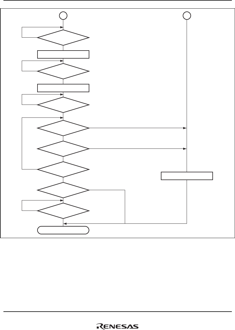
24. Multimedia Card Interface (MMCIF)
Rev.1.00 Jan. 10, 2008 Page 1253 of 1658
REJ09B0261-0100
End of command sequence
Set CMDOFF to 1
Set the DATAEN bit to 1
DRPI interrupt
detected?
No
Ye s
DBSYI interrupt
detected?
No
Ye s
CRCERI interrupt
detected?
Ye s
No
DTERI interrupt
detected?
Ye s
No
DTBUSY detected?
No
Ye s
FRDYI interrupt
detected or DMA transfer
end?
No
Ye s
Clear DMACR to H'00
DMA transfer end?
No
Ye s
DTI interrupt
detected?
No
Ye s
12
Figure 24.26 (2) Example of Write Sequence Flow (Single Block Transfer)
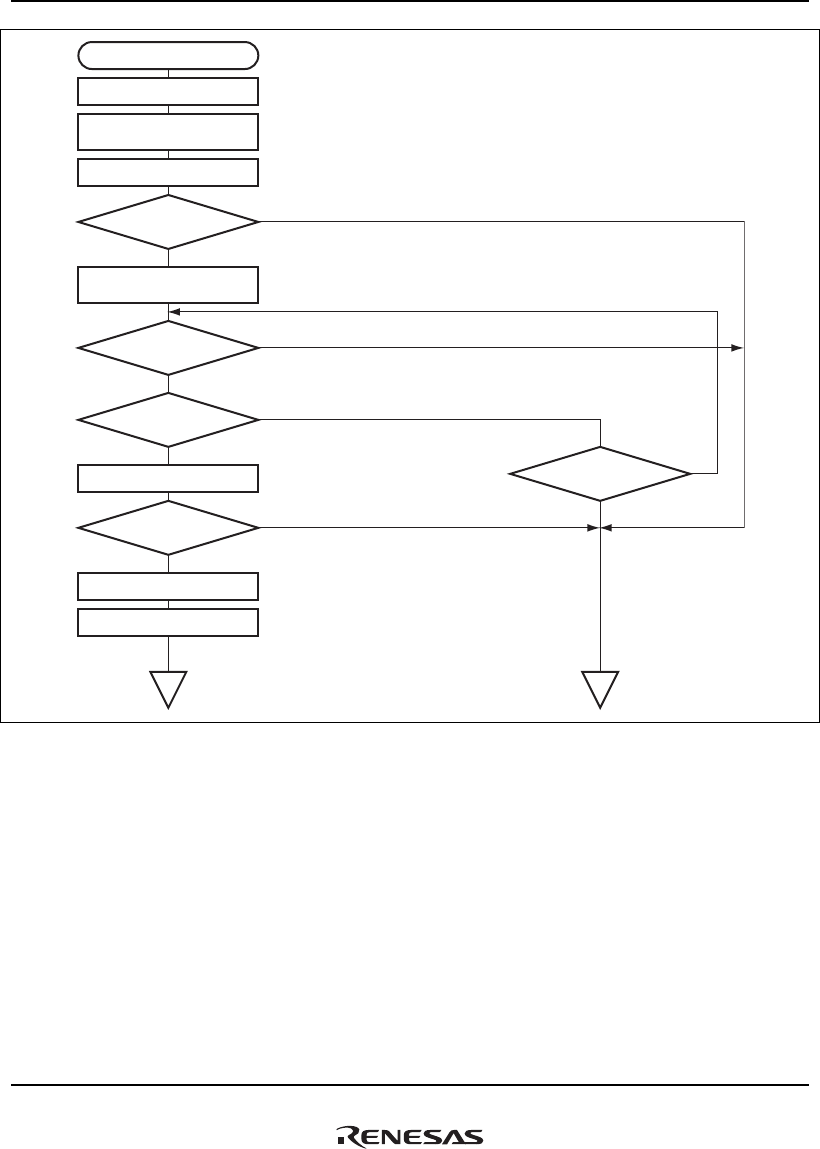
24. Multimedia Card Interface (MMCIF)
Rev.1.00 Jan. 10, 2008 Page 1254 of 1658
REJ09B0261-0100
Start of command sequence
Clear FIFO
Execute CMD16
Configure the DMAC
Set DMACR (in the MMCIF)
Read response register
CMD16
normal end?
No
Ye s
CRPI interrupt
detected?
No
Ye s
Response status
normal?
No
Ye s
CTERI interrupt
detected?
No
Ye s
CRCERI interrupt
detected?
Ye s
No
Set the block size in TBCR
Execute CMD 25
(Set CMDR then CMDSTRT)
1 2
Figure 24.27 (1) Example of Write Sequence Flow (Open-ended Multiple Block Transfer)
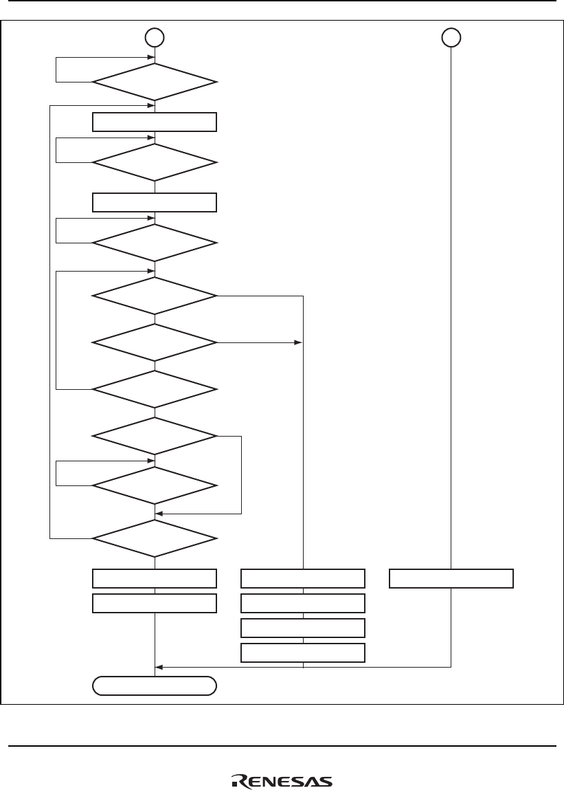
24. Multimedia Card Interface (MMCIF)
Rev.1.00 Jan. 10, 2008 Page 1255 of 1658
REJ09B0261-0100
End of command sequence
Set DATAEN to 1
DRPI interrupt
detected?
No
Ye s
DBSYI interrupt
detected?
No
Ye s
CRCERI
or WRERI interrupt
detected?
Ye s
No
DTERI interrupt
detected?
Ye s
No
Next block write?
No
Ye s
DTBUSY detected?
No
Ye s
FRDYI interrupt
detected or DMA transfer
end?
No
Ye s
Clear DMACR to H'00
DMA transfer end?
No
Ye s
DTI interrupt
detected?
No
Ye s
12
Set CMDOFF to 1
Clear FIFO
Clear DMACR to H'00
Execute CMD12 or Stop Tran
Set CMDOFF to 1
Execute CMD12 or Stop Tran
Set CMDOFF to 1
Figure 24.27 (2) Example of Write Sequence Flow (Open-ended Multiple Block Transfer)
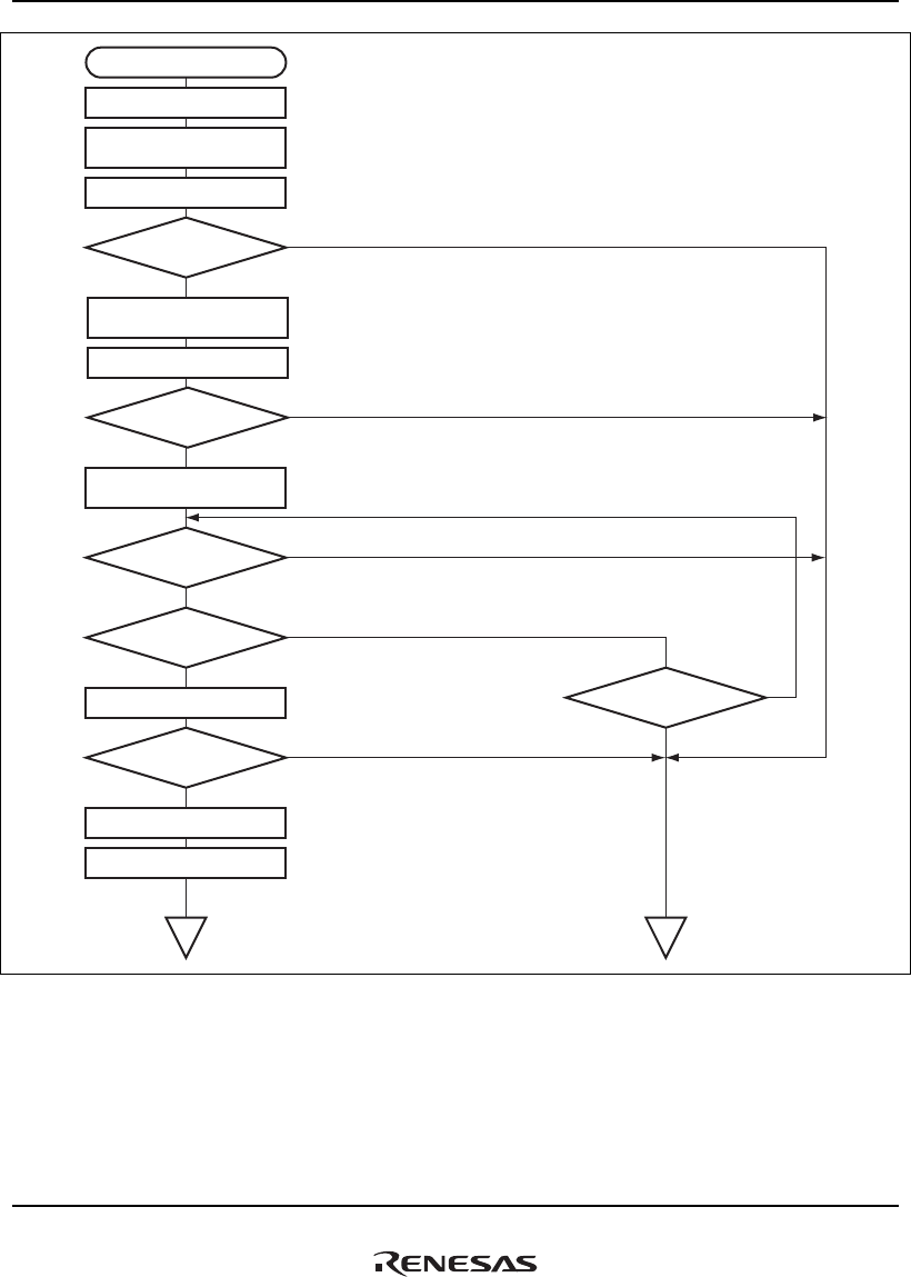
24. Multimedia Card Interface (MMCIF)
Rev.1.00 Jan. 10, 2008 Page 1256 of 1658
REJ09B0261-0100
Start of command sequence
Clear FIFO
Execute CMD16
Configure the DMAC
Set DMACR (in the MMCIF)
Read response register
CMD16
normal end?
No
Ye s
CRPI interrupt
detected?
No
Ye s
Response status
normal?
No
Ye s
CTERI interrupt
detected?
No
Ye s
CRCERI interrupt
detected?
Ye s
No
Set the block size in TBCR
Execute CMD 25
(Set CMDR then CMDSTRT)
1 2
Set the number of
blocks in TBNCR
Execute CMD 23
CMD 23
normal end?
No
Ye s
Figure 24.27 (3) Example of Write Sequence Flow (Pre-defined Multiple Block Transfer)
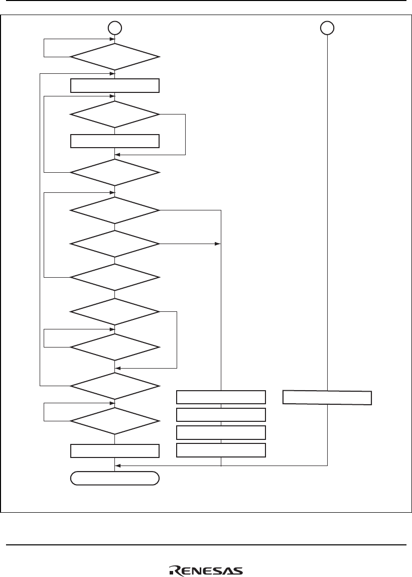
24. Multimedia Card Interface (MMCIF)
Rev.1.00 Jan. 10, 2008 Page 1257 of 1658
REJ09B0261-0100
End of command sequence
Set DATAEN to 1
DRPI interrupt
detected?
No
Ye s
DBSYI interrupt
detected?
No
Ye s
CRCERI
or WRERI interrupt
detected?
Ye s
No
No
DTERI interrupt
detected?
Ye s
No
BTI interrupt
detected?
No
Ye s
TBNCR = n (DRPI)?
No
Ye s
DTBUSY detected?
No
Ye s
FRDYI interrupt
detected or DMA transfer
end?
No
Ye s
Clear DMACR to H'00
DMA transfer end?
Ye s
DTI interrupt
detected?
No
Ye s
1 2
Set CMDOFF to 1
Clear FIFO
Clear DMACR to H'00
Execute CMD12 or Stop Tran
Set CMDOFF to 1
Set CMDOFF to 1
Legend:
n (DRPI): Number of data response interrupts (DRPI) from the start of write sequence
Figure 24.27 (4) Example of Write Sequence Flow (Pre-defined Multiple Block Transfer)

24. Multimedia Card Interface (MMCIF)
Rev.1.00 Jan. 10, 2008 Page 1258 of 1658
REJ09B0261-0100
Start of command sequence
Clear FIFO
Configure the DMAC
Set DMACR (in the MMCIF)
Read response register
CRPI interrupt
detected?
No
Ye s
Response status
normal?
No
Ye s
CTERI interrupt
detected?
No
Ye s
CRCERI interrupt
detected?
Ye s
No
Execute CMD 20
(Set CMDR then CMDSTRT)
End of command sequence
Set DATAEN to 1
FRDYI interrupt
detected or DMA transfer
end?
No
Ye s
Clear DMACR to H'00
DMA transfer end?
No
Ye s
FEI interrupt
detected?
No
Ye s
Set CMDOFF to 1
Execute CMD12
Set CMDOFF to 1
Figure 24.28 Example of Operational Flow for Stream Write Transfer
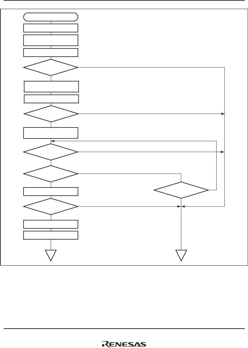
24. Multimedia Card Interface (MMCIF)
Rev.1.00 Jan. 10, 2008 Page 1259 of 1658
REJ09B0261-0100
Start of command sequence
Clear FIFO
Execute CMD16
Configure the DMAC
Set DMACR (in the MMCIF)
Read response register
CMD16
normal end?
No
Ye s
CRPI interrupt
detected?
No
Ye s
Response status
normal ended?
No
Ye s
CTERI interrupt
detected?
No
Ye s
CRCERI interrupt
detected?
Ye s
No
Set the block size in TBCR
Execute CMD 25
(Set CMDR then CMDSTRT)
1 2
Set the number of
blocks in TBNCR
Execute CMD 23
CMD 23
normal end?
No
Ye s
Figure 24.29 (1) Example of Operational Flow for Auto-mode
Pre-defined Multiple Block Write Transfer
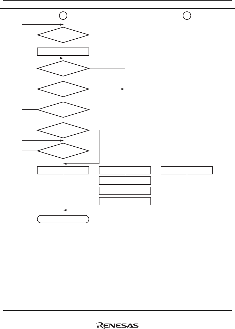
24. Multimedia Card Interface (MMCIF)
Rev.1.00 Jan. 10, 2008 Page 1260 of 1658
REJ09B0261-0100
End of command sequence
BTI interrupt
detected?
No
Ye s
DBSYI interrupt
detected?
No
Ye s
CRCERI
or WRERI interrupt
detected?
Ye s
No
DTERI interrupt
detected?
Ye s
No
DTBUSY detected?
No
Ye s
Clear DMACR to H'00
DMA transfer end?
No
Ye s
12
Set CMDOFF to 1
Clear FIFO
Clear DMACR to H'00
Execute CMD12 or Stop Tran
Set CMDOFF to 1Set CMDOFF to 1
Figure 24.29 (2) Example of Operational Flow for Auto-mode
Pre-defined Multiple Block Write Transfer

24. Multimedia Card Interface (MMCIF)
Rev.1.00 Jan. 10, 2008 Page 1261 of 1658
REJ09B0261-0100
24.7 Register Accesses with Little Endian Specification
When the little endian is specified, the access size for registers or that for memory where the
corresponding data is stored should be fixed. For example, if data read from the MMCIF with the
word size is written to memory and then it is read from memory with the byte size, data
misalignment occurs.

24. Multimedia Card Interface (MMCIF)
Rev.1.00 Jan. 10, 2008 Page 1262 of 1658
REJ09B0261-0100

25. Audio Codec Interface (HAC)
Rev.1.00 Jan. 10, 2008 Page 1263 of 1658
REJ09B0261-0100
Section 25 Audio Codec Interface (HAC)
The HAC, the audio codec digital controller interface, supports a subset of Audio Codec 97
(AC'97) Version 2.1. The HAC provides serial transmission to/reception from the AC97 codec.
Each channel of the HAC can be connected to a single audio codec device.
The HAC carries out data extraction from/insertion into audio frames. For data slots within both
receive and transmit frames, the PIO transfer by the CPU or the DMA transfer by the DMAC can
be used.
25.1 Features
The HAC has the following features:
• Supports a subset of digital interface to a single AC'97 revision 2.1 Audio Codec
• PIO transfer of status slots 1 and 2 in RX frames
• PIO transfer of command slots 1 and 2 in TX frames
• PIO transfer of data slots 3 and 4 in RX frames
• PIO transfer of data slots 3 and 4 in TX frames
• Selectable 16-bit or 20-bit DMA transfer of data slots 3 and 4 in RX frames
• Selectable 16-bit or 20-bit DMA transfer of data slots 3 and 4 in TX frames
• Accommodates various sampling rates by qualifying slot data with tag bits and monitoring the
TX frame request bits of RX frames
• Generates data ready, data request, overrun and underrun interrupts
• Supports cold reset, warm reset, and power-down mode
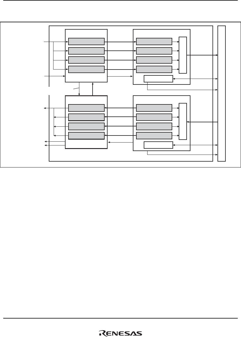
25. Audio Codec Interface (HAC)
Rev.1.00 Jan. 10, 2008 Page 1264 of 1658
REJ09B0261-0100
Figure 25.1 shows a block diagram of the HAC.
HAC receiver
Shift register for slot 1
Shift register for slot 2
Shift register for slot 3
Shift register for slot 4
Internal bus interface (Reception)
CSAR RX buffer
CSDR RX buffer
PCML RX buffer
PCMR RX buffer
DMA control
DMA request
Interrupt request
Internal bus interface (Transmission)
CSAR TX buffer
CSDR TX buffer
PCML TX buffer
PCMR TX buffer
DMA control
HAC transmitter
Shift register for slot 1
Shift register for slot 2
Shift register for slot 3
Shift register for slot 4
DMA request
Data[19:0]
Data[19:0]
Data[31:0]
Data[31:0]
Data[19:0]
Data[19:0]
Control signal
Bit control signal
Interrupt request
Data[19:0]
Data[19:0]
Data[19:0]
Data[19:0]
Control signal
Peripheral bus
Request signal
for slots 3 and 4
HACn_SDIN
HACn_BITCLK
HACn_SDOUT
HACn_SYNC
HACn_RES
Note: n = 0 to 1
Figure 25.1 Block Diagram

25. Audio Codec Interface (HAC)
Rev.1.00 Jan. 10, 2008 Page 1265 of 1658
REJ09B0261-0100
25.2 Input/Output Pins
Table 25.1 describes the HAC pin configuration.
Table 25.1 Pin Configuration
Pin Name Pin Count I/O Function
HAC0_BITCLK 1 Input Serial data clock
HAC0_SDIN 1 Input RX frame serial input data
HAC0_SDOUT 1 Output TX frame serial output data
HAC0_SYNC 1 Output Frame sync
HAC1_BITCLK 1 Input Serial data clock
HAC1_SDIN 1 Input RX frame serial input data
HAC1_SDOUT 1 Output TX frame serial output data
HAC1_SYNC 1 Output Frame sync
HAC_RES 1 Output Reset (negative logic signal) (common to channels
0 and 1)

25. Audio Codec Interface (HAC)
Rev.1.00 Jan. 10, 2008 Page 1266 of 1658
REJ09B0261-0100
25.3 Register Descriptions
The following shows the HAC registers. In this manual, the registers are not discriminated by the
channel.
Table 25.2 Register Configuration (1)
Channel Register Name Abbrev. R/W
P4
Address
Area 7
Address Size
Sync
Clock
0 Control and status register 0 HACCR0 R/W H'FFE3 0008 H'1FE3 0008 32 Pck
0 Command/status address
register 0
HACCSAR0 R/W H'FFE3 0020 H'1FE3 0020 32 Pck
0 Command/status data register 0 HACCSDR0 R/W H'FFE3 0024 H'1FE3 0024 32 Pck
0 PCM left channel register 0 HACPCML0 R/W H'FFE3 0028 H'1FE3 0028 32 Pck
0 PCM right channel register 0 HACPCMR0 R/W H'FFE3 002C H'1FE3 002C 32 Pck
0 TX interrupt enable register 0 HACTIER0 R/W H'FFE3 0050 H'1FE3 0050 32 Pck
0 TX status register 0 HACTSR0 R/W H'FFE3 0054 H'1FE3 0054 32 Pck
0 RX interrupt enable register 0 HACRIER0 R/W H'FFE3 0058 H'1FE3 0058 32 Pck
0 RX status register 0 HACRSR0 R/W H'FFE3 005C H'1FE3 005C 32 Pck
0 HAC control register 0 HACACR0 R/W H'FFE3 0060 H'1FE3 0060 32 Pck
1 Control and status register 1 HACCR1 R/W H'FFE4 0008 H'1FE4 0008 32 Pck
1 Command/status address
register 1
HACCSAR1 R/W H'FFE4 0020 H'1FE4 0020 32 Pck
1 Command/status data register 1 HACCSDR1 R/W H'FFE4 0024 H'1FE4 0024 32 Pck
1 PCM left channel register 1 HACPCML1 R/W H'FFE4 0028 H'1FE4 0028 32 Pck
1 PCM right channel register 1 HACPCMR1 R/W H'FFE4 002C H'1FE4 002C 32 Pck
1 TX interrupt enable register 1 HACTIER1 R/W H'FFE4 0050 H'1FE4 0050 32 Pck
1 TX status register 1 HACTSR1 R/W H'FFE4 0054 H'1FE4 0054 32 Pck
1 RX interrupt enable register 1 HACRIER1 R/W H'FFE4 0058 H'1FE4 0058 32 Pck
1 RX status register 1 HACRSR1 R/W H'FFE4 005C H'1FE4 005C 32 Pck
1 HAC control register 1 HACACR1 R/W H'FFE4 0060 H'1FE4 0060 32 Pck

25. Audio Codec Interface (HAC)
Rev.1.00 Jan. 10, 2008 Page 1267 of 1658
REJ09B0261-0100
Table 25.2 Register Configuration (2)
Channel Register Name Abbrev.
Power-on
Reset by
PRESET
Pin/WDT/
H-UDI
Manual
Reset by
WDT/
Multiple
Exceptions
Sleep by
Sleep
Instruction
Module
Standby
Deep
Sleep
0 Control and status
register 0
HACCR0 H'0000 0200 H'0000 0200 Retained Retained Retained
0 Command/status
address register 0
HACCSAR0 H'0000 0000 H'0000 0000 Retained Retained Retained
0 Command/status
data register 0
HACCSDR0 H'0000 0000 H'0000 0000 Retained Retained Retained
0 PCM left channel
register 0
HACPCML0 H'0000 0000 H'0000 0000 Retained Retained Retained
0 PCM right channel
register 0
HACPCMR0 H'0000 0000 H'0000 0000 Retained Retained Retained
0 TX interrupt enable
register 0
HACTIER0 H'0000 0000 H'0000 0000 Retained Retained Retained
0 TX status register
0
HACTSR0 H'F000 0000 H'F000 0000 Retained Retained Retained
0 RX interrupt
enable register 0
HACRIER0 H'0000 0000 H'0000 0000 Retained Retained Retained
0 RX status register
0
HACRSR0 H'0000 0000 H'0000 0000 Retained Retained Retained
0 HAC control
register 0
HACACR0 H'8400 0000 H'8400 0000 Retained Retained Retained

25. Audio Codec Interface (HAC)
Rev.1.00 Jan. 10, 2008 Page 1268 of 1658
REJ09B0261-0100
Channel Register Name Abbrev.
Power-on
Reset by
PRESET
Pin/WDT/
H-UDI
Manual
Reset by
WDT/
Multiple
Exceptions
Sleep by
Sleep
Instruction
Module
Standby
Deep
Sleep
1 Control and status
register 1
HACCR1 H'0000 0200 H'0000 0200 Retained Retained Retained
1 Command/status
address register 1
HACCSAR1 H'0000 0000 H'0000 0000 Retained Retained Retained
1 Command/status
data register 1
HACCSDR1 H'0000 0000 H'0000 0000 Retained Retained Retained
1 PCM left channel
register 1
HACPCML1 H'0000 0000 H'0000 0000 Retained Retained Retained
1 PCM right channel
register 1
HACPCMR1 H'0000 0000 H'0000 0000 Retained Retained Retained
1 TX interrupt enable
register 1
HACTIER1 H'0000 0000 H'0000 0000 Retained Retained Retained
1 TX status register
1
HACTSR1 H'F000 0000 H'F000 0000 Retained Retained Retained
1 RX interrupt
enable register 1
HACRIER1 H'0000 0000 H'0000 0000 Retained Retained Retained
1 RX status register
1
HACRSR1 H'0000 0000 H'0000 0000 Retained Retained Retained
1 HAC control
register 1
HACACR1 H'8400 0000 H'8400 0000 Retained Retained Retained

25. Audio Codec Interface (HAC)
Rev.1.00 Jan. 10, 2008 Page 1269 of 1658
REJ09B0261-0100
25.3.1 Control and Status Register (HACCR)
HACCR is a 32-bit read/write register for controlling input/output and monitoring the interface
status.
31 30 29 28 27 26 25 24 23 22 21 20 19 18 17 16
⎯⎯⎯⎯⎯⎯⎯⎯⎯⎯⎯⎯
⎯⎯⎯⎯⎯⎯⎯⎯⎯⎯⎯⎯
⎯⎯⎯⎯
Bit:
0000000000000000
Initial value:
RRRRRRRRRRRRRRRR
RRWRRRRR
R/W:
Bit:
Initial value:
R/W:
15 14 13 12 11 10 9 8 7 6 5 4 3 2 1 0
00000010 0000 000
RRRRWWRR
CR CDRT WMRT ST
0
Bit Bit Name
Initial
Value R/W Description
31 to 16 ⎯ All 0 R Reserved
These bits are always read as 0. The write value should
always be 0.
15 CR 0 R Codec Ready
0: The HAC-connected codec is not ready.
1: The HAC-connected codec is ready.
14 to 12 ⎯ All 0 R Reserved
These bits are always read as 0. Write prohibited.
11 CDRT 0 W HAC Cold Reset
Use a cold reset only after power-on, or only to exit
from the power-down mode by the power-down
command.
[Write]
0: Always write 0 to this bit before writing 1 again.
(When this bit is changed from 0 to 1, a cold reset is
performed.)
1: Performs a cold reset on the HAC-connected codec.
[Read]
Always read as 0.

25. Audio Codec Interface (HAC)
Rev.1.00 Jan. 10, 2008 Page 1270 of 1658
REJ09B0261-0100
Bit Bit Name
Initial
Value R/W Description
10 WMRT 0 W HAC Warm Reset
Use a warm reset only after power-up, or only to exit
from the power-down mode by the power-down
command.
[Write]
0: Always write 0 to this bit before writing 1 again.
(When this bit is changed from 0 to 1, a warm reset is
performed.)
1: Performs a warm reset on the HAC-connected
codec.
[Read]
Always read as 0.
9 ⎯ 1 R Reserved
This bit is always read as 1. The write value should
always be 1.
8 to 6 ⎯ All 0 R Reserved
These bits are always read as 0. The write value should
always be 0.
5 ST 0 W Start Transfer
[Write]
0: Stops data transmission/reception at the end of the
current frame. Do not take this action to terminate
transmission/reception in normal operation. When
terminating transmission/reception in normal
operation, refer to the following description.
1: Starts data transmission/reception.
[Read]
Always read as 0.
4 to 0 ⎯ All 0 R Reserved
These bits are always read as 0. The write value should
always be 0.
To place the off-chip codec device into the power-down mode, write 1 to bit 12 of the register
index 26 in the off-chip codec via the HAC. When entering the power-down mode, the off-chip
codec stops HAC_BITCLK and suspends the normal operation. The off-chip codec acts in the
same manner at power-on. To resume the normal operation, perform a cold reset or a warm reset
on the off-chip codec.

25. Audio Codec Interface (HAC)
Rev.1.00 Jan. 10, 2008 Page 1271 of 1658
REJ09B0261-0100
25.3.2 Command/Status Address Register (HACCSAR)
HACCSAR is a 32-bit read/write register that specifies the address of the codec register to be read
/written. When requesting a write to/read from a codec register, write the command register
address to HACCSAR and set the ST bit in the HACCR register to 1. The HAC then transmits this
register address to the codec via slot 1.
After the codec has responded to a read request (HACRSR.STARY = 1), the status address
received via slot 1 can be read out from HACCSAR.
31 30 29 28 27 26 25 24 23 22 21 20 19 18 17 16
⎯⎯⎯⎯⎯⎯⎯⎯⎯⎯⎯⎯
⎯
⎯
Bit:
0000000000000000
Initial value:
R R R R R R R R R R R R R/W R/W R/W R/W
RRRRRRRR
R/W:
Bit:
Initial value:
R/W:
1514131211109876543210
00000000 0000 000
R/W R/W R/W R/W R R R R
CA3/
SA3
CA2/
SA2
CA1/
SA1
CA0/
SA0
SLR
EQ3
SLR
EQ4
SLR
EQ5
SLR
EQ6
SLR
EQ7
SLR
EQ8
SLR
EQ9
SLR
EQ10
SLR
EQ11
SLR
EQ12
CA6/
SA6
RW CA5/
SA5
CA4/
SA4
0
Bit Bit Name
Initial
Value R/W Description
31 to 20 ⎯ All 0 R Reserved
These bits are always read as 0. The write value should
always be 0.
19 RW 0 R/W Codec Read/Write Command
0: Notifies the off-chip codec device of a write access to
the register specified in the address field (CA6/SA6
to CA0/SA0).
Write the data to HACCSDR in advance.
When HACACR.TX12_ATOMIC is 1, the HAC
transmits HACCSAR and HACCSDR as a pair in the
same TX frame.
When HACACR.TX12_ATOMIC is 0, transmission of
HACCSAR and HACCSDR in the same TX frame is
not guaranteed.
1: Notifies the off-chip codec device of a read access to
the register specified in the address field (CA6/SA6
to CA0/SA0).

25. Audio Codec Interface (HAC)
Rev.1.00 Jan. 10, 2008 Page 1272 of 1658
REJ09B0261-0100
Bit Bit Name
Initial
Value R/W Description
18
17
16
15
14
13
12
CA6/SA6
CA5/SA5
CA4/SA4
CA3/SA3
CA2/SA2
CA1/SA1
CA0/SA0
0
0
0
0
0
0
0
R/W
R/W
R/W
R/W
R/W
R/W
R/W
Codec Control Register Addresses 6 to 0/Codec Status
Register Addresses 6 to 0
[Write]
Specify the address of the codec register to be written.
[Read]
Indicate the status address received via slot 1,
corresponding to the codec register whose data has
been returned in HACCSDR.
11
10
9
8
7
6
5
4
3
2
SLREQ3
SLREQ4
SLREQ5
SLREQ6
SLREQ7
SLREQ8
SLREQ9
SLREQ10
SLREQ11
SLREQ12
0
0
0
0
0
0
0
0
0
0
R
R
R
R
R
R
R
R
R
R
Slot Requests 3 to 12
Valid only in the RX frame. Indicate whether the codec
is requesting slot data in the next TX frame.
Automatically set by hardware, and correspond to bits
11 to 2 of slot 1 in the RX frame.
0: Slot data is requested.
1: Slot data is not requested.
1, 0 ⎯ All 0 R Reserved
These bits are always read as 0. The write value should
always be 0.

25. Audio Codec Interface (HAC)
Rev.1.00 Jan. 10, 2008 Page 1273 of 1658
REJ09B0261-0100
25.3.3 Command/Status Data Register (HACCSDR)
HACCSDR is a 32-bit read/write data register used for accessing the codec register. Write the
command data to HACCSDR and set the ST bit in the HACCR register to 1. The HAC then
transmits the data to the codec via slot 2.
After the codec has responded to a read request (HACRSR.STDRY = 1), the status data received
via slot 2 can be read out from HACCSDR. In both read and write, HACCSAR stores the related
codec register address.
31 30 29 28 27 26 25 24 23 22 21 20 19 18 17 16
⎯⎯⎯⎯⎯⎯⎯⎯⎯⎯⎯⎯
⎯⎯⎯
⎯
Bit:
0000000000000000
Initial value:
R R R R R R R R R R R R R/W R/W R/W R/W
R/W R/W R/W R/W R R R R
R/W:
Bit:
Initial value:
R/W:
1514131211109876543210
00000000 0000 000
R/W R/W R/W R/W R/W R/W R/W R/W
CD11/
SD11
CD10/
SD10
CD9/
SD9
CD8/
SD8
CD7/
SD7
CD6/
SD6
CD5/
SD5
CD4/
SD4
CD3/
SD3
CD2/
SD2
CD1/
SD1
CD0/
SD0
CD15/
SD15
CD14/
SD14
CD13/
SD13
CD12/
SD12
0

25. Audio Codec Interface (HAC)
Rev.1.00 Jan. 10, 2008 Page 1274 of 1658
REJ09B0261-0100
Bit Bit Name
Initial
Value R/W Description
31 to 20 ⎯ All 0 R Reserved
These bits are always read as 0. The write value should
always be 0.
19
18
17
16
15
14
13
12
11
10
9
8
7
6
5
4
CD15/SD15
CD14/SD14
CD13/SD13
CD12/SD12
CD11/SD11
CD10/SD10
CD9/SD9
CD8/SD8
CD7/SD7
CD6/SD6
CD5/SD5
CD4/SD4
CD3/SD3
CD2/SD2
CD1/SD1
CD0/SD0
0
0
0
0
0
0
0
0
0
0
0
0
0
0
0
0
R/W
R/W
R/W
R/W
R/W
R/W
R/W
R/W
R/W
R/W
R/W
R/W
R/W
R/W
R/W
R/W
Command Data 15 to 0/Status Data 15 to 0
Write data to these bits and then write the codec
register address in HACCSAR. The HAC then transmits
the data to the codec.
Read these bits to get the contents of the codec register
indicated by HACCSAR.
3 to 0 ⎯ All 0 R Reserved
These bits are always read as 0. The write value should
always be 0.

25. Audio Codec Interface (HAC)
Rev.1.00 Jan. 10, 2008 Page 1275 of 1658
REJ09B0261-0100
25.3.4 PCM Left Channel Register (HACPCML)
HACPCML is a 32-bit read/write register used for accessing the left channel of the codec in
digital audio recording or stream playback. To transmit the PCM playback left channel data to the
codec, write the data to HACPCML. To receive the PCM record left channel data from the codec,
read HACPCML. The data is left justified when accommodating a codec with ADC/DAC
resolution of 20 bits or less.
31 30 29 28 27 26 25 24 23 22 21 20 19 18 17 16
⎯⎯⎯⎯⎯⎯⎯⎯⎯⎯⎯
⎯
Bit:
0000000000000000
Initial value:
R R R R R R R R R R R R R/W R/W R/W R/W
R/W R/W R/W R/W R/W R/W R/W R/W
R/W:
Bit:
Initial value:
R/W:
1514131211109876543210
00000000 0000 000
R/W R/W R/W R/W R/W R/W R/W R/W
D19 D18 D17 D16
D3 D2 D1 D0D7 D6 D5 D4D11 D10 D9 D8D15 D14 D13 D12
0
Bit Bit Name
Initial
Value R/W Description
31 to 20 ⎯ All 0 R Reserved
These bits are always read as 0. The write value should
always be 0.
19 to 0 D19 to D0 All 0 R/W Data 19 to 0
Write the PCM playback left channel data to these bits.
The HAC then transmits the data to the codec on an on-
demand basis.
Read these bits to get the PCM record left channel data
from the codec.

25. Audio Codec Interface (HAC)
Rev.1.00 Jan. 10, 2008 Page 1276 of 1658
REJ09B0261-0100
In 16-bit packed DMA mode, HACPCML is defined as follows:
31 30 29 28 27 26 25 24 23 22 21 20 19 18 17 16
-
Bit:
0000000000000000
Initial value:
R/W R/W R/W R/WR/W R/W R/W R/WR/W R/W R/W R/WR/W R/W R/W R/W
R/W R/W R/W R/W R/W R/W R/W R/W
R/W:
Bit:
Initial value:
R/W:
1514131211109876543210
00000000 0000 000
R/W R/W R/W R/W R/W R/W R/W R/W
RD3 RD1RD2 RD0RD7 RD6 RD5 RD4RD11 RD10 RD9 RD8RD15 RD14 RD13 RD12
LD3 LD1LD2 LD0LD7 LD6 LD5 LD4LD11 LD10 LD9 LD8LD15 LD14 LD13 LD12
0
Bit Bit Name
Initial
Value R/W Description
31 to 16 LD15 to LD0 All 0 R/W Left Data 15 to 0
Write the PCM playback left channel data to these bits.
The HAC then transmits the data to the codec on an on-
demand basis.
Read these bits to get the PCM record left channel data
from the codec.
15 to 0 RD15 to RD0 All 0 R/W Right Data 15 to 0
Write the PCM playback right channel data to these
bits. The HAC then transmits the data to the codec on
an on-demand basis.
Read these bits to get the PCM record right channel
data from the codec.

25. Audio Codec Interface (HAC)
Rev.1.00 Jan. 10, 2008 Page 1277 of 1658
REJ09B0261-0100
25.3.5 PCM Right Channel Register (HACPCMR)
HACPCMR is a 32-bit read/write register used for accessing the right channel of the codec in
digital audio recording or stream playback. To transmit the PCM playback right channel data to
the codec, write the data to HACPCMR. To receive the PCM record right channel data from the
codec, read HACPCMR. The data is left justified when accommodating a codec with ADC/DAC
resolution of 20 bits or less.
31 30 29 28 27 26 25 24 23 22 21 20 19 18 17 16
⎯⎯⎯⎯⎯⎯⎯⎯⎯⎯⎯
⎯
Bit:
0000000000000000
Initial value:
R R R R R R R R R R R R R/W R/W R/W R/W
R/W R/W R/W R/W R/W R/W R/W R/W
R/W:
Bit:
Initial value:
R/W:
1514131211109876543210
00000000 0000 000
R/W R/W R/W R/W R/W R/W R/W R/W
D19 D18 D17 D16
D3 D2 D1 D0D7 D6 D5 D4D11 D10 D9 D8D15 D14 D13 D12
0
Bit Bit Name
Initial
Value R/W Description
31 to 20 ⎯ All 0 R Reserved
These bits are always read as 0. The write value should
always be 0.
19 to 0 D19 to D0 All 0 R/W Data 19 to 0
Write the PCM playback right channel data to these
bits. The HAC then transmits the data to the codec on
an on-demand basis.
Read these bits to get the PCM record right channel
data from the codec.

25. Audio Codec Interface (HAC)
Rev.1.00 Jan. 10, 2008 Page 1278 of 1658
REJ09B0261-0100
25.3.6 TX Interrupt Enable Register (HACTIER)
HACTIER is a 32-bit read/write register that enables or disables HAC TX interrupts.
31 30 29 28 27 26 25 24 23 22 21 20 19 18 17 16
⎯⎯⎯⎯⎯⎯⎯⎯⎯⎯⎯⎯⎯⎯
⎯⎯ ⎯⎯⎯⎯⎯
⎯
Bit:
0000000000000000
Initial value:
RRR/WR/WRRRRRRRRRRRR
RRRRRRRR
R/W:
Bit:
Initial value:
R/W:
15 14 13 12 11 10 9 8 7 6 5 4 3 2 1 0
00000000 0000 000
R R R R R R R/W R/W
PLTF
UNIE
PRTF
UNIE
⎯⎯⎯ ⎯⎯⎯
PLTF
RQIE
PRTF
RQIE
0
Bit Bit Name
Initial
Value R/W Description
31, 30 ⎯ All 0 R Reserved
These bits are always read as 0. The write value should
always be 0.
29 PLTFRQIE 0 R/W PCML TX Request Interrupt Enable
0: Disables PCML TX request interrupts.
1: Enables PCML TX request interrupts.
28 PRTFRQIE 0 R/W PCMR TX Request Interrupt Enable
0: Disables PCMR TX request interrupts.
1: Enables PCMR TX request interrupts.
27 to 10 ⎯ All 0 R Reserved
These bits are always read as 0. The write value should
always be 0.
9 PLTFUNIE 0 R/W PCML TX Underrun Interrupt Enable
0: Disables PCML TX underrun interrupts.
1: Enables PCML TX underrun interrupts.
8 PRTFUNIE 0 R/W PCMR TX Underrun Interrupt Enable
0: Disables PCMR TX underrun interrupts.
1: Enables PCMR TX underrun interrupts.
7 to 0 ⎯ All 0 R Reserved
These bits are always read as 0. The write value should
always be 0.

25. Audio Codec Interface (HAC)
Rev.1.00 Jan. 10, 2008 Page 1279 of 1658
REJ09B0261-0100
25.3.7 TX Status Register (HACTSR)
HACTSR is a 32-bit read/write register that indicates the status of the HAC TX controller. Writing
0 to the bit will initialize it.
31 30 29 28 27 26 25 24 23 22 21 20 19 18 17 16
⎯⎯⎯⎯⎯⎯⎯⎯⎯⎯⎯⎯
⎯⎯ ⎯⎯⎯⎯⎯
⎯
Bit:
1111000000000000
Initial value:
R/W R/W R/W R/W R R R R R R R R R R R R
RRRRRRRR
R/W:
Bit:
Initial value:
R/W:
1514131211109876543210
00000000 0000 000
R R R R R R R/W R/W
PLT
FUN
PRT
FUN
⎯⎯⎯ ⎯⎯⎯
PLT
FRQ
CMD
DMT
CMD
AMT
PRT
FRQ
0
Bit Bit Name
Initial
Value R/W*2 Description
31 CMDAMT 1 R/W Command Address Empty
0: CSAR TX buffer contains untransmitted data.
1: CSAR TX buffer is empty and ready to store data.*1
30 CMDDMT 1 R/W Command Data Empty
0: CSDR TX buffer contains untransmitted data.
1: CSDR TX buffer is empty and ready to store data. *1
29 PLTFRQ 1 R/W PCML TX Request
0: PCML TX buffer contains untransmitted data.
1: PCML TX buffer is empty and needs to store data. In
DMA mode, writing to HACPCML will automatically
clear this bit to 0.
28 PRTFRQ 1 R/W PCMR TX Request
0: PCMR TX buffer contains untransmitted data.
1: PCMR TX buffer is empty and needs to store data. In
DMA mode, writing to HACPCMR will automatically
clear this bit to 0.

25. Audio Codec Interface (HAC)
Rev.1.00 Jan. 10, 2008 Page 1280 of 1658
REJ09B0261-0100
Bit Bit Name
Initial
Value R/W*2 Description
27 to 10 ⎯ All 0 R Reserved
These bits are always read as 0. The write value should
always be 0.
9 PLTFUN 0 R/W PCML TX Underrun
0: No PCML TX underrun has occurred.
1: PCML TX underrun has occurred because the codec
has requested slot 3 data but new data is not written
to HACPCML.
8 PRTFUN 0 R/W PCMR TX Underrun
0: No PCMR TX underrun has occurred.
1: PCMR TX underrun has occurred because the codec
has requested slot 4 data but new data is not written
to HACPCMR.
7 to 0 ⎯ All 0 R Reserved
These bits are always read as 0. The write value should
always be 0.
Notes: 1. CMDAMT and CMDDMT have no associated interrupts. Poll these bits until they are
read as 1 before writing a new command to HACCSAR/HACCSDR. When bit 19 (RW)
of HACCSAR is 0 and TX12_ATOMIC is 1, take the following steps:
1. Initialize CMDDMT and CMDAMT before first accessing a codec register after HAC
initialization by any reset event.
2. After making the settings in HACCSDR and HACCSAR, poll CMDDMT and
CMDAMT until they are cleared to 1, and then initialize these bits.
3. Now the next write to a register is available.
2. These bits are readable/writable. Writing 0 to the bit initializes it but writing 1 has no
effect.

25. Audio Codec Interface (HAC)
Rev.1.00 Jan. 10, 2008 Page 1281 of 1658
REJ09B0261-0100
25.3.8 RX Interrupt Enable Register (HACRIER)
HACRIER is a 32-bit read/write register that enables or disables HAC RX interrupts.
31 30 29 28 27 26 25 24 23 22 21 20 19 18 17 16
⎯⎯⎯⎯⎯⎯⎯⎯⎯⎯⎯⎯
⎯⎯⎯⎯ ⎯⎯⎯⎯⎯
⎯
Bit:
0000000000000000
Initial value:
R R R R R R R R R R/W R/W R/W R/W R R R
RRRRRRRR
R/W:
Bit:
Initial value:
R/W:
1514131211109876543210
00000000 0000 000
R R R/W R/W R R R R
PLRF
OVIE
PRRF
OVIE
⎯⎯ ⎯⎯
PLRF
RQIE
STDR
YIE
STAR
YIE
PRRF
RQIE
0
Bit Bit Name
Initial
Value R/W Description
31 to 23 ⎯ All 0 R Reserved
These bits are always read as 0. The write value should
always be 0.
22 STARYIE 0 R/W Status Address Ready Interrupt Enable
0: Disables status address ready interrupts.
1: Enables status address ready interrupts.
21 STDRYIE 0 R/W Status Data Ready Interrupt Enable
0: Disables status data ready interrupts.
1: Enables status data ready interrupts.
20 PLRFRQIE 0 R/W PCML RX Request Interrupt Enable
0: Disables PCML RX request interrupts.
1: Enables PCML RX request interrupts.
19 PRRFRQIE 0 R/W PCMR RX Request Interrupt Enable
0: Disables PCMR RX request interrupts.
1: Enables PCMR RX request interrupts.
18 to 14 ⎯ All 0 R Reserved
These bits are always read as 0. The write value should
always be 0.
13 PLRFOVIE 0 R/W PCML RX Overrun Interrupt Enable
0: Disables PCML RX overrun interrupts.
1: Enables PCML RX overrun interrupts.

25. Audio Codec Interface (HAC)
Rev.1.00 Jan. 10, 2008 Page 1282 of 1658
REJ09B0261-0100
Bit Bit Name
Initial
Value R/W Description
12 PRRFOVIE 0 R/W PCMR RX Overrun Interrupt Enable
0: Disables PCMR RX overrun interrupts.
1: Enables PCMR RX overrun interrupts.
11 to 0 ⎯ All 0 R Reserved
These bits are always read as 0. The write value should
always be 0.
25.3.9 RX Status Register (HACRSR)
HACRSR is a 32-bit read/write register that indicates the status of the HAC RX controller.
Writing 0 to the bit will initialize it.
31 30 29 28 27 26 25 24 23 22 21 20 19 18 17 16
⎯⎯⎯ ⎯⎯⎯⎯⎯⎯ ⎯⎯ ⎯
⎯⎯⎯⎯ ⎯⎯⎯⎯⎯
⎯
Bit:
0000000000000000
Initial value:
R R R R R R R R R R/W R/W R/W R/W R R R
RRRRRRRR
R/W:
Bit:
Initial value:
R/W:
1514131211109876543210
00000000 0000 000
R R R/W R/W R R R R
⎯⎯ ⎯⎯
STARY STDRY
PLR
FRQ
PRR
FRQ
PLR
FOV
PRR
FOV
0

25. Audio Codec Interface (HAC)
Rev.1.00 Jan. 10, 2008 Page 1283 of 1658
REJ09B0261-0100
Bit Bit Name
Initial
Value R/W* Description
31 to 23 ⎯ All 0 R Reserved
These bits are always read as 0. The write value should
always be 0.
22 STARY 0 R/W Status Address Ready
0: HACCSAR (status address) is not ready.
1: HACCSAR (status address) is ready.
21 STDRY 0 R/W Status Data Ready
0: HACCSDR (status data) is not ready.
1: HACCSDR (status data) is ready.
20 PLRFRQ 0 R/W PCML RX Request
0: PCML RX data is not ready.
1: PCML RX data is ready and must be read. In DMA
mode, reading HACPCML automatically clears this
bit to 0.
19 PRRFRQ 0 R/W PCMR RX Request
0: PCMR RX data is not ready.
1: PCMR RX data is ready and must be read. In DMA
mode, reading HACPCMR automatically clears this
bit to 0.
18 to 14 ⎯ All 0 R Reserved
These bits are always read as 0. The write value should
always be 0.
13 PLRFOV 0 R/W PCML RX Overrun
0: No PCML RX data overrun has occurred.
1: PCML RX data overrun has occurred because the
HAC has received new data from slot 3 before PCML
data is not read out.
12 PRRFOV 0 R/W PCMR RX Overrun
0: No PCMR RX data overrun has occurred.
1: PCMR RX data overrun has occurred because the
HAC has received new data from slot 4 before PCMR
data is not read out.
11 to 0 ⎯ All 0 R Reserved
These bits are always read as 0. The write value should
always be 0.
Note: * This register is readable/writable. Writing 0 to the bit initializes it but writing 1 has no
effect.

25. Audio Codec Interface (HAC)
Rev.1.00 Jan. 10, 2008 Page 1284 of 1658
REJ09B0261-0100
25.3.10 HAC Control Register (HACACR)
HACACR is a 32-bit read/write register used for controlling the HAC interface.
31 30 29 28 27 26 25 24 23 22 21 20 19 18 17 16
⎯⎯⎯⎯ ⎯⎯⎯⎯ ⎯
⎯⎯⎯⎯ ⎯⎯⎯⎯⎯
⎯
Bit:
1000010000000000
Initial value:
R R/W R/W R R R/W R R/W R/W R/W R/W R R R R R
RRRRRRRR
R/W:
Bit:
Initial value:
R/W:
15 14 13 12 11 10 9 8 7 6 5 4 3 2 1 0
00000000 0000 000
RRRRRRRR
⎯⎯ ⎯⎯⎯⎯
TX12_
ATOMIC
RXDMAL
_EN
TXDMAL
_EN
RXDMAR
_EN
TXDMAR
_EN
DMA
RX16
DMA
TX16
0
Bit Bit Name
Initial
Value R/W Description
31 ⎯ 1 R Reserved
This bit is always read as 1. The write value should
always be 1.
30 DMARX16 0 R/W 16-bit RX DMA Enable
0: Disables 16-bit packed RX DMA mode. Enables the
RXDMAL_EN and RXDMAR_EN settings.
1: Enables 16-bit packed RX DMA mode. Disables the
RXDMAL_EN and RXDMAR_EN settings.
29 DMATX16 0 R/W 16-bit TX DMA Enable
0: Disables 16-bit packed TX DMA mode. Enables the
TXDMAL_EN and TXDMAR_EN settings.
1: Enables 16-bit packed TX DMA mode. Disables the
TXDMAL_EN and TXDMAR_EN settings.
28, 27 ⎯ All 0 R Reserved
These bits are always read as 0. The write value should
always be 0.
26 TX12_ATOMIC 1 R/W TX Slot 1 and 2 Atomic Control
0: Transmits TX data in HACCSAR and that in
HACCSDR separately. (Setting prohibited)
1: Transmits TX data in HACCSAR and that in
HACCSDR in the same frame if bit 19 in HACCSAR
is 0 (write). (HACCSAR must be written last.)

25. Audio Codec Interface (HAC)
Rev.1.00 Jan. 10, 2008 Page 1285 of 1658
REJ09B0261-0100
Bit Bit Name
Initial
Value R/W Description
25 ⎯ 0 R Reserved
This bit is always read as 0. The write value should
always be 0.
24 RXDMAL_EN 0 R/W RX DMA Left Enable
0: Disables 20-bit RX DMA for HACPCML.
1: Enables 20-bit RX DMA for HACPCML.
23 TXDMAL_EN 0 R/W TX DMA Left Enable
0: Disables 20-bit TX DMA for HACPCML.
1: Enables 20-bit TX DMA for HACPCML.
22 RXDMAR_EN 0 R/W RX DMA Right Enable
0: Disables 20-bit RX DMA for HACPCMR.
1: Enables 20-bit RX DMA for HACPCMR.
21 TXDMAR_EN 0 R/W TX DMA Right Enable
0: Disables 20-bit TX DMA for HACPCMR.
1: Enables 20-bit TX DMA for HACPCMR.
20 to 0 ⎯ All 0 R Reserved
These bits are always read as 0. The write value should
always be 0.
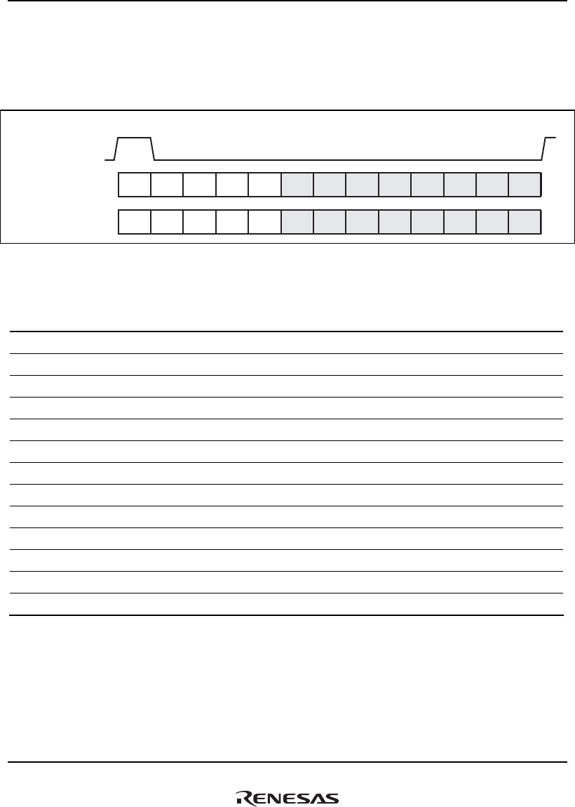
25. Audio Codec Interface (HAC)
Rev.1.00 Jan. 10, 2008 Page 1286 of 1658
REJ09B0261-0100
25.4 AC 97 Frame Slot Structure
Figure 25.2 shows the AC97 frame slot structure. This LSI supports slots 0 to 4 only. Slots 5 to 12
(hatched area) are out of scope.
Slot No.
TAG CMD
Data
CMD
Addr
PCML
Front
LINE1
DAC
PCMR
Front
PCM
Center
PCMR
Surr
PCML
Surr
PCM
LFE
HSET
DAC
IO
CTRL
LINE2
DAC
0123456789101112
HAC_SYNC
HAC_SDOUT (transmit)
HAC_SDIN (receive) TAG Status
Data
Status
Addr
PCM
Left
LINE1
ADC
PCM
Right
PCM
MIC
Reser
ved
Reser
ved
Reser
ved
HSET
ADC
IO
Status
LINE2
ADC
Figure 25.2 AC97 Frame Slot Structure
Table 25.3 AC97 Transmit Frame Structure
Slot Name Description
0 SDATA_OUT TAG Codec IDs and Tags indicating valid data
1 Control CMD Addr write port Read/write command and register address
2 Control DATA write port Register write data
3 PCM L DAC playback Left channel PCM output data
4 PCM R DAC playback Right channel PCM output data
5 Modem Line 1 DAC Modem 1 output data (unsupported)*
6 PCM Center Center channel PCM data (unsupported)*
7 PCM Surround L Surround left channel PCM data (unsupported)*
8 PCM Surround R Surround right channel PCM data (unsupported)*
9 PCM LFE LFE channel PCM data (unsupported)*
10 Modem Line 2 DAC Modem 2 output data (unsupported)*
11 Modem handset DAC Modem handset output data (unsupported)*
12 Modem IO control Modem control IO output (unsupported)*
Note: * There is no register for unsupported functions.

25. Audio Codec Interface (HAC)
Rev.1.00 Jan. 10, 2008 Page 1287 of 1658
REJ09B0261-0100
Table 25.4 AC97 Receive Frame Structure
Slot Name Description
0 SDATA_IN TAG Tags indicating valid data
1 Status ADDR read port Register address and slot request
2 Status DATA read port Register read data
3 PCM L ADC record Left channel PCM input data
4 PCM R ADC record Right channel PCM input data
5 Modem Line 1 ADC Modem 1 input data (unsupported)*
6 Dedicated Microphone ADC Optional PCM data (unsupported)*
7 to 9 Reserved Reserved
10 Modem Line 2 ADC Modem 2 input data (unsupported)*
11 Modem handset input DAC Modem handset input data (unsupported)*
12 Modem IO status Modem control IO input (unsupported)*
Note: * There is no register for unsupported functions.

25. Audio Codec Interface (HAC)
Rev.1.00 Jan. 10, 2008 Page 1288 of 1658
REJ09B0261-0100
25.5 Operation
25.5.1 Receiver
The HAC receiver receives serial audio data input on the HAC_SDIN pin, synchronous to
HAC_BITCLK. From slot 0, the receiver extracts tag bits that indicate which other slots contain
valid data. It will update the receive data only when receiving valid slot data indicated by the tag
bits.
Supporting data only in slots 1 to 4, the receiver ignores tag bits and data related to slots 5 to 12. It
loads valid slot data to the corresponding shift register to hold the data for PIO or DMA transfer,
and sets the corresponding status bits. It is possible to read 20-bit data within a 32-bit register
using PIO.
In the case of RX overrun, the new data will overwrite the current data in the RX buffer of the
HAC.
25.5.2 Transmitter
The HAC transmitter outputs serial audio data on the HAC_SDOUT pin, synchronous to
HAC_BIT_CLK. The transmitter sets the tag bits in slot 0 to indicate which slots in the current
frame contain valid data. It loads data slots to the current TX frame in response to the
corresponding slot request bits from the previous RX frame.
The transmitter supports data only in slots 1 to 4. The TX buffer holds data that has been
transferred using PIO or DMA, and sets the corresponding status bit. It is possible to write 20-bit
data within a 32-bit register using PIO.
In the case of a TX underrun, the HAC will transmit the current TX buffer data until the next data
arrives.

25. Audio Codec Interface (HAC)
Rev.1.00 Jan. 10, 2008 Page 1289 of 1658
REJ09B0261-0100
25.5.3 DMA
The HAC supports DMA transfer for slots 3 and 4 of both the RX and TX frames. Specify the slot
data size for DMA transfer, 16 or 20 bits, with the DMARX16 and DMATX16 bits in HACACR.
When the data size is 20 bits, transfer of data slots 3 and 4 requires two local bus access cycles.
Since each of the receiver and transmitter has its DMA request, the stereo mode generates a DMA
request for slots 3 and 4 separately. The mono mode generates a DMA request for just one slot.
When the data size is 16 bits, data from slots 3 and 4 are packed into a single 32-bit quantity (left
data and right data are in PCML), which requires only one local bus access cycle.
It may be necessary to halt a DMA transfer before the end count is reached, depending on system
applications. If so, clear the corresponding DMA bit in HACACR to 0 (DMA disabled). To
resume a DMA transfer, reprogram the DMAC and then set the corresponding DMA bit to 1
(DMA enabled).
25.5.4 Interrupts
Interrupts can be used for flag events from the receiver and transmitter. Make the setting for each
interrupt in the corresponding interrupt enable register. Interrupts include a request to the CPU to
read/write slot data, overrun and underrun. To get the interrupt source, read the status register.
Writing 0 to the bit will clear the corresponding interrupt.
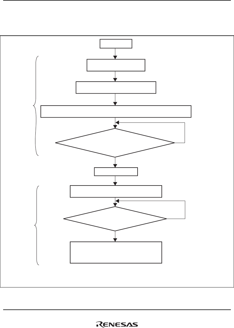
25. Audio Codec Interface (HAC)
Rev.1.00 Jan. 10, 2008 Page 1290 of 1658
REJ09B0261-0100
25.5.5 Initialization Sequence
Figure 25.3 shows an example of the initialization sequence.
No
No
Yes
HAC module
initialization
External codec
device
initialization
START
HAC cold reset
(HACCR = H'0000 0A00)
Start transfer (receiver/transmitter)
(HACCR = H'0000 0220)
Enable TX/RX
(Set HACACR to H'05E0 0000: 20-bit DMA, TX slots and 2 atomic control)*
1
Codec ready?
(Set HACCCR to H'0000 8000: 20-bit DMA,
TX slots and 2 atomic control)*
1
Set DMAC
*2
Set read address to #h'26 (Power-down mode Ctrl/Stat)
(Set HACCSAR to H'000A 6000)*
1
Off-chip codec internal status
ADC, DAC, Analog, REF = ready?
(Set HACCSDR to H'0000 00F0)*
1
Set read volume and sampling rate
(1) HACACR = H'0000 0000
(2) Set HACCSAR and HACCSDR
(3) HACACR = H'01E0 0000
Notes: 1. Register values are reference data.
2. For details on DMAC settings, refer to section 14, Direct Memory Access Controller (DMAC)
Figure 25.3 Initialization Sequence
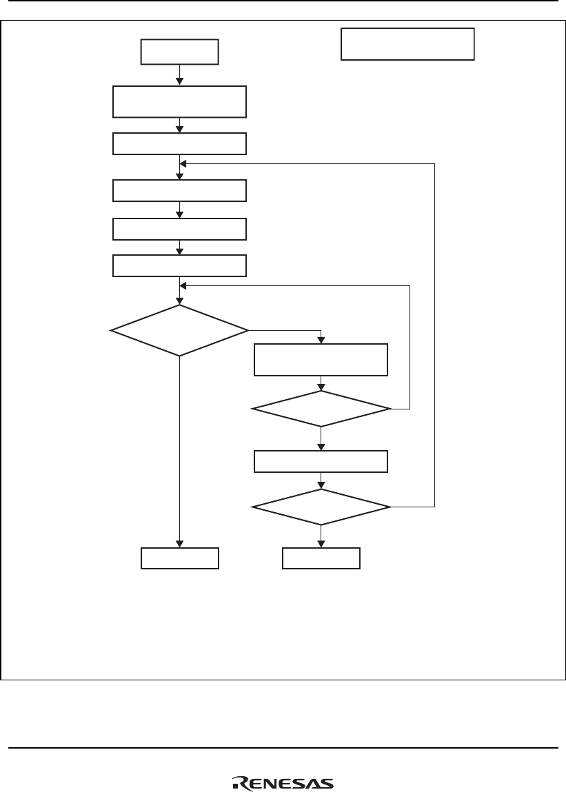
25. Audio Codec Interface (HAC)
Rev.1.00 Jan. 10, 2008 Page 1291 of 1658
REJ09B0261-0100
No
No
Yes
Yes
Yes
Write to codec
Return Error
Write 0 to TSR.CMDAMT
Write 0 to TSR.CMDDMT
Prerequisite:
ACR.TX12_ATOMIC = 1
Wait for 1 μs
LoopCnt++
Clear RetryCnt to 0
Set data in CSDR
Set Addr. in CSAR
No
Clear LoopCnt to 0
RetryCnt++
TSR.CMDAMT = 1 &
TSR.CMDDMT = 1
E1 < LoopCnt 1
5 < RetryCnt
Notes: E1: Loop count required in the target system
(21 < E1 < 1000)
Input: Addr: Address of codec register to be written to
Data: Data to be written to codec register
RetryCnt: Software counter for error detection
LoopCnt: Software counter for wait insertion
Figure 25.4 Sample Flowchart for Off-Chip Codec Register Write
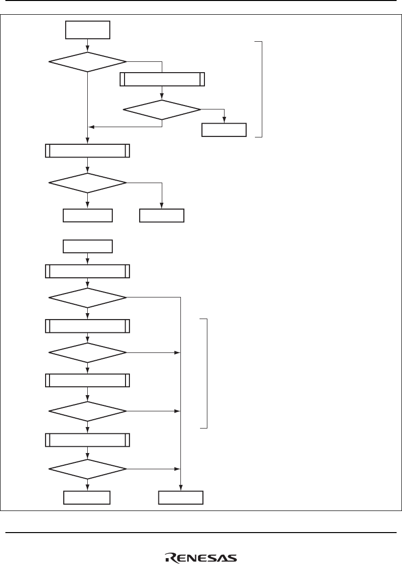
25. Audio Codec Interface (HAC)
Rev.1.00 Jan. 10, 2008 Page 1292 of 1658
REJ09B0261-0100
Read codec
No
Yes
No
Yes
No
Yes
Yes
Yes
Yes
No
Yes
RegV = H'7C
(Vender ID1)
Last_Reg: Address of the register
read last time
Dummy read
Dummy processing
(Discard the first data)
Read_codec_aux (RegN)
RegN = Last_Reg?
Error
Data return
Error
Error
Error
Error
Error
Error
ErrorData 2 return
Read_codec_aux
Send_read_request (RegN)
Send_read_request (RegN)
Get_codec_data (RegN)
Get_codec_data (RegN)
Read_codec_aux (RegV)
No
No
No
Error
: Data acquisition
: Data 1 acquisition
: Data 2 acquisition
Input: RegN (address of the codec register to be read)
Input: RegN (address of the codec register to be read)
In continuous reading of registers in some off-chip codec
devices, the data in the register previously read may be read
again. In such case, take the steps in this flowchart.
Figure 25.5 Sample Flowchart for Off-Chip Codec Register Read (1)
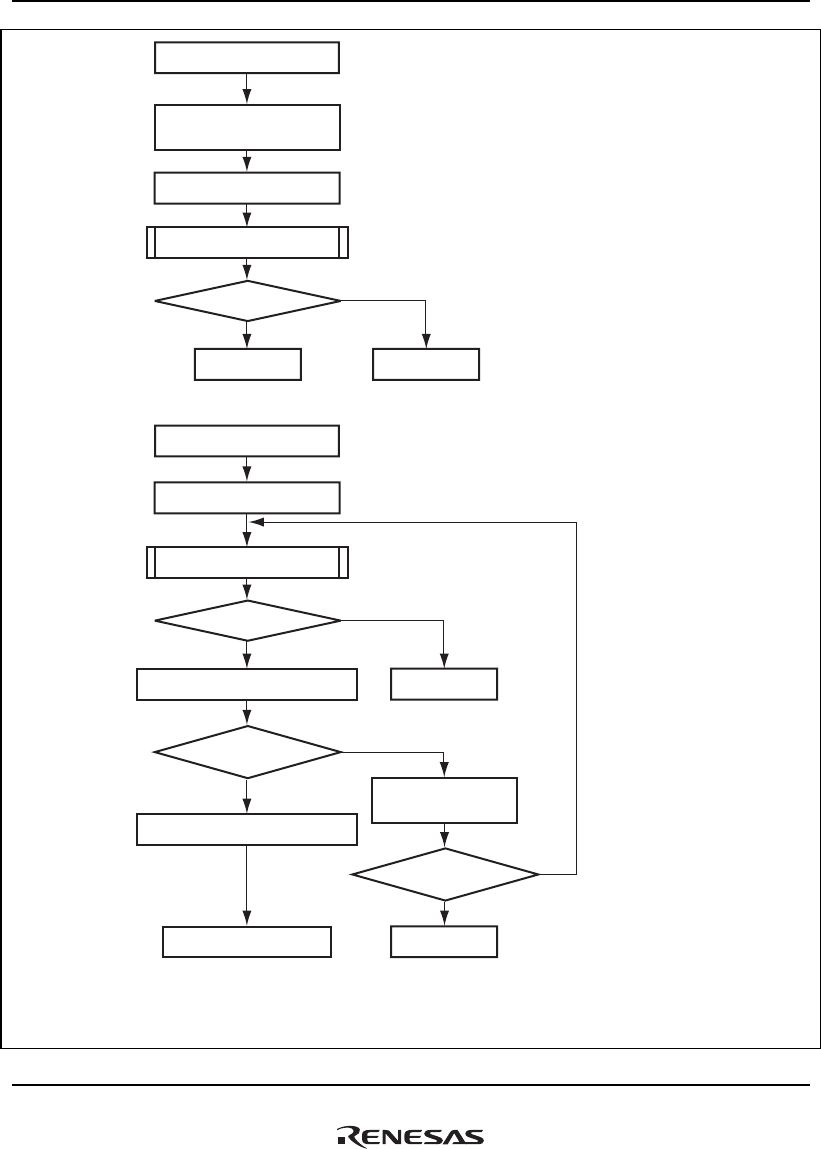
25. Audio Codec Interface (HAC)
Rev.1.00 Jan. 10, 2008 Page 1293 of 1658
REJ09B0261-0100
No
Yes
Send_read_request
Write 0 to RSR.STARY
Write 0 to RSR.STDRY
Notes: E2: Loop count required in the target system (13 < E2)
LoopCnt2: Software counter for wait insertion
Addr: Variable to hold CSAR read value.
DataT: Variable to hold CSDR read value.
Set RegN in CSAR
WaitLoop_CMDAMT
Error
Error
Error
Error
Error
Return
Wait for 5 μs
LoopCnt 2 ++
No
No
Yes
Yes
No
Yes
Get_codec_data Input: RegN (address of the codec register to be read)
Input: RegN (address of the codec register to be read)
Clear LoopCnt 2 to 0
WaitLoop_RSR
Assign HACCSAR read value to Addr
Addr (R) = RegN?
E2 < LoopCnt 2
Assign HACCSDR read value to Data T
Data T is returned
Figure 25.6 Sample Flowchart for Off-Chip Codec Register Read (2)
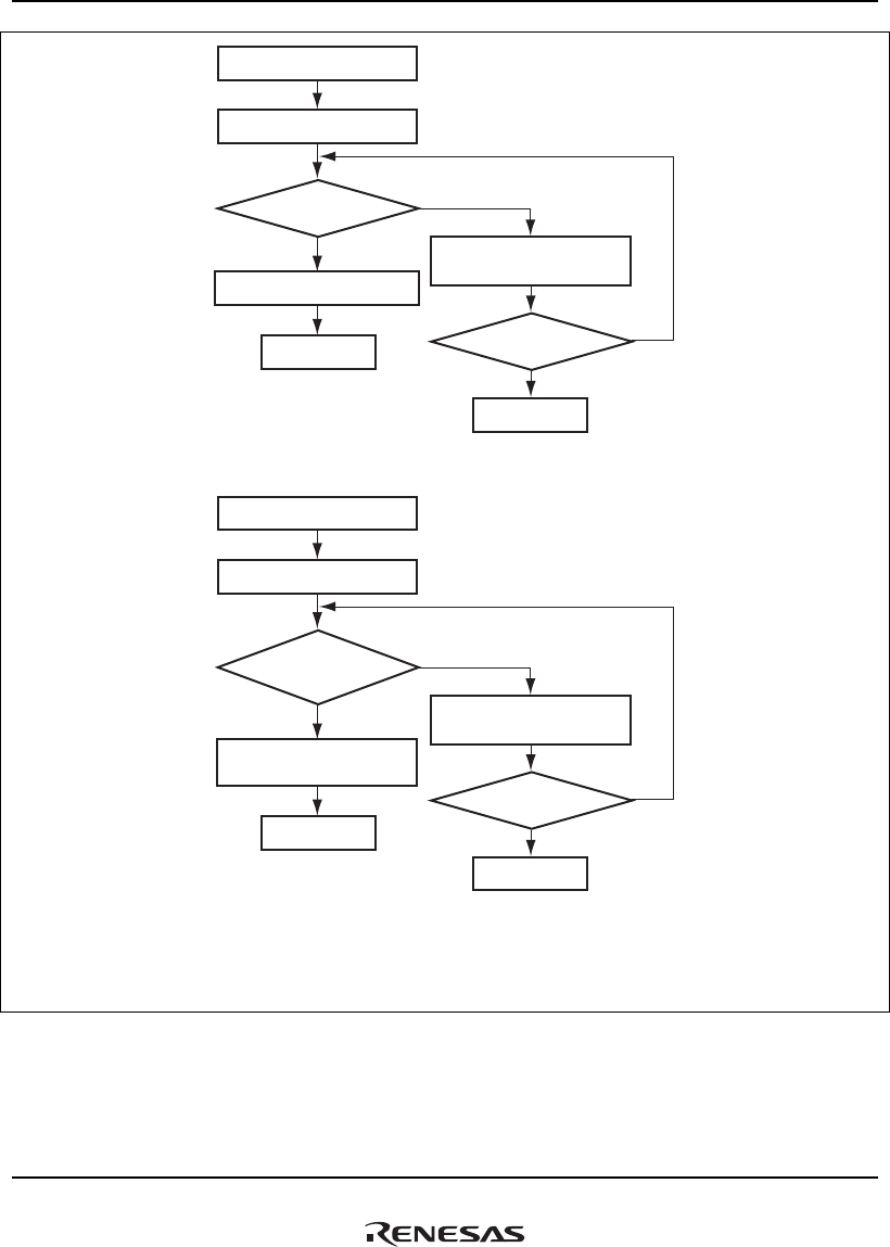
25. Audio Codec Interface (HAC)
Rev.1.00 Jan. 10, 2008 Page 1294 of 1658
REJ09B0261-0100
No
No
Yes
WaitLoop_CMDAMT
Notes: E3, E4: Loop count required in the target system
(21 < E3, 21 < E4 < 1000)
LoopCnt3: Software counter for wait insertion
LoopCnt4: Software counter for wait insertion
Write 0 to TSR.CMDAMT
Return
Return
Error
Clear LoopCnt 3 to 0
TSR.CMDAMT = 1
Wait for 1 μs
LoopCnt 3 ++
Yes
E3 < LoopCnt 3
Error
No
No
Yes
WaitLoop_RSR
Write 0 to RSR.STARY
Write 0 to RSR.STDRY
Clear LoopCnt 4 to 0
RSR.STARY = 1 &
RSR.STDRY = 1
Wait for 1 μs
LoopCnt 4 ++
Yes
E4 < LoopCnt 4
Figure 25.7 Sample Flowchart for Off-Chip Codec Register Read (3)

25. Audio Codec Interface (HAC)
Rev.1.00 Jan. 10, 2008 Page 1295 of 1658
REJ09B0261-0100
25.5.6 Power-Down Mode
It is possible to stop or resume the supply of clock to the HAC using the MSTP16 and MSTP17
bits in the standby control register 0 (MSTPCR0), which is a register used in power-down modes.
To cancel module standby function and resume the supply of clock to the HAC, write 0 to the
MSTP16 and MSTP17 bits in the standby control register 0 (MSTPCR0). It enables all accesses to
the HAC.
To place the HAC into the power-down mode, take the following steps:
1. Check that all data transfers have ended. Also check that the transmit buffer is empty and the
receive buffer has been read out to be empty.
2. Disable all DMA requests and interrupt requests.
3. Place the codec into power-down mode.
4. Write 0 to the MSTP16 and MSTP17 bits in the standby control register 0 (MSTPCR0).
25.5.7 Notes
The HAC_SYNC signal is generated by the HAC to indicate the position of slot 0 within a frame.
When using the two channels of the HAC concurrently, connect the HAC_RES pin to the reset
pins of the two codecs.
25.5.8 Reference
AC'97 Component Specification, Revision 2.1

25. Audio Codec Interface (HAC)
Rev.1.00 Jan. 10, 2008 Page 1296 of 1658
REJ09B0261-0100

26. Serial Sound Interface (SSI) Module
Rev.1.00 Jan. 10, 2008 Page 1297 of 1658
REJ09B0261-0100
Section 26 Serial Sound Interface (SSI) Module
This LSI incorporates two channels of serial sound interface (SSI) modules that send or receive
audio data to or from a variety of devices. In addition to the common formats, they support burst
and multi-channel mode.
26.1 Features
The SSI has the following features.
• Number of channels: Two channels
• Operating modes: Compressed mode and non-compressed mode
The compressed mode is used for continuous bit stream transfer
The non-compressed mode supports all serial audio streams divided into channels.
• The SSI module is configured as any of a transmitter or receiver. The serial bus format (refer
to table 26.3) can be used in the compressed and non-compressed mode.
• Asynchronous transfer between the data buffer and the shift register
• Division ratios of the serial bus interface clock can be selected.
• Data transmission/reception can be controlled from the DMAC or SSI interrupt.
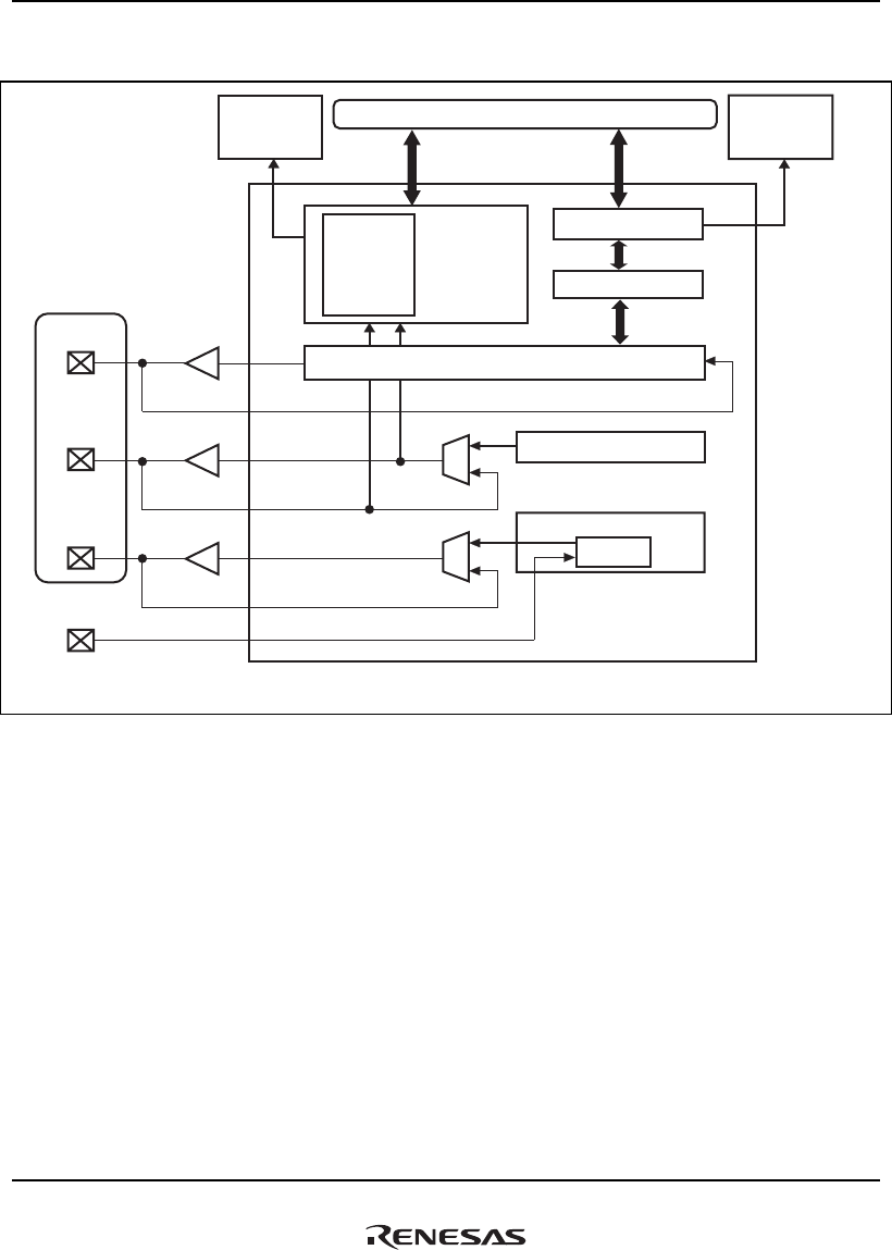
26. Serial Sound Interface (SSI) Module
Rev.1.00 Jan. 10, 2008 Page 1298 of 1658
REJ09B0261-0100
Figure 26.1 is a block diagram of the SSI module.
Serial audio bus
SSIn_SDATA
SSIn_WS
SSIn_SCK
SSIn_CLK
INTC DMAC
DMA request
Interrupt
request
Peripheral bus
Control circuit Register
SSICR
SSISR
SSITDR
SSIRDR
Data buffer
Barrel shifter
MSB Shift register
Bit counter
Serial clock control
SSI module
Divider
LSB
Note: n = 0 to 1
Figure 26.1 Block Diagram of SSI Module

26. Serial Sound Interface (SSI) Module
Rev.1.00 Jan. 10, 2008 Page 1299 of 1658
REJ09B0261-0100
26.2 Input/Output Pins
Table 26.1 lists the pin configurations relating to the SSI module.
Table 26.1 Pin Configuration
Name
Number of
Pins I/O Function
SSI0_SCK 1 I/O Serial bit clock
SSI0_WS 1 I/O Word select
SSI0_SDATA 1 I/O Serial data input/output
SSI0_CLK 1 Input Divider input clock (oversampling clock
256/384/512fs input)
SSI1_SCK 1 I/O Serial bit clock
SSI1_WS 1 I/O Word select
SSI1_SDATA 1 I/O Serial data input/output
SSI1_CLK 1 Input Divider input clock (oversampling clock
256/384/512fs input)

26. Serial Sound Interface (SSI) Module
Rev.1.00 Jan. 10, 2008 Page 1300 of 1658
REJ09B0261-0100
26.3 Register Descriptions
The SSI has the following registers. In this manual, the register description is not discriminated
by the channel.
Table 26.2 Register Configuration (1)
Channel Register Name Abbrev. R/W P4 Address
Area 7
Address Size
Sync
Clock
0 Control register 0 SSICR0 R/W H'FFE0 0000 H'1FE0 0000 32 Pck
0 Status register 0 SSISR0 R/W* H'FFE0 0004 H'1FE0 0004 32 Pck
0 Transmit data register 0 SSITDR0 R/W H'FFE0 0008 H'1FE0 0008 32 Pck
0 Receive data register 0 SSIRDR0 R H'FFE0 000C H'1FE0 000C 32 Pck
1 Control register 1 SSICR1 R/W H'FFE1 0000 H'1FE1 0000 32 Pck
1 Status register 1 SSISR1 R/W* H'FFE1 0004 H'1FE1 0004 32 Pck
1 Transmit data register 1 SSITDR1 R/W H'FFE1 0008 H'1FE1 0008 32 Pck
1 Receive data register 1 SSIRDR1 R H'FFE1 000C H'1FE1 000C 32 Pck
Note: Bits 26 and 27 of this register is readable/writable. The other bits are read only. For
details, see section 26.3.2, Status Register (SSISR).
Table 26.2 Register Configuration (2)
Channel Register Name Abbrev.
Power-on
Reset by
PRESET Pin/
WDT/H-UDI
Manual Reset
by WDT/
Multiple
Exception
Sleep by
SLEEP
Instruction
Module
Standby
Deep
Sleep
0 Control register 0 SSICR0 H'0000 0000 H'0000 0000 Retained Retained Retained
0 Status register 0 SSISR0 H'0200 0003 H'0200 0003 Retained Retained Retained
0 Transmit data
register 0
SSITDR0 H'0000 0000 H'0000 0000 Retained Retained Retained
0 Receive data
register 0
SSIRDR0 H'0000 0000 H'0000 0000 Retained Retained Retained
1 Control register 1 SSICR1 H'0000 0000 H'0000 0000 Retained Retained Retained
1 Status register 1 SSISR1 H'0200 0003 H'0200 0003 Retained Retained Retained
1 Transmit data
register 1
SSITDR1 H'0000 0000 H'0000 0000 Retained Retained Retained
1 Receive data
register 1
SSIRDR1 H'0000 0000 H'0000 0000 Retained Retained Retained

26. Serial Sound Interface (SSI) Module
Rev.1.00 Jan. 10, 2008 Page 1301 of 1658
REJ09B0261-0100
26.3.1 Control Register (SSICR)
SSICR is a 32-bit readable/writable register that controls interrupts, selects each polarity status,
and sets operating mode.
31 30 29 28 27 26 25 24 23 22 21 20 19 18 17 16
0⎯⎯ 000⎯000000000
BRENPDTASDTA DELSWSP SPDPSWSDSCKD SCKP MUEN CPEN TRMD EN
CHNL1 CHNL0 DWL2IIENOIEN DIENDMEN UIEN DWL1
CKDV2 CKDV1 CKDV0
DWL0 SWL2 SWL1 SWL0
Bit:
Initial value:
R/W:
Bit:
Initial value:
R/W:
1514131211109876543210
R R R R/W R/W R/W R/W R/WR/W R/W R/W R/WR/WR/WR/W R/W
0000000000000000
R/W R/W R/W R/W R/W R/W R/W R/WR/W R/W R/W R/WR/WR/WR/W R/W
⎯⎯
⎯
Bit Bit Name
Initial
Value R/W Description
31 to 29 ⎯ 0 R Reserved
These bits are always read as an undefined value. The
write value should always be 0.
28 DMEN 0 R/W DMA Enable
Enables or disables the DMA request.
0: DMA request disabled.
1: DMA request enabled.
27 UIEN 0 R/W Underflow Interrupt Enable
0: Underflow interrupt disabled
1: Underflow interrupt enabled
26 OIEN 0 R/W Overflow Interrupt Enable
0: Overflow interrupt disabled
1: Overflow interrupt enabled
25 IIEN 0 R/W Idle Mode Interrupt Enable
0: Idle mode interrupt disabled
1: Idle mode interrupt enabled
24 DIEN 0 R/W Data Interrupt Enable
0: Data interrupt disabled
1: Data interrupt enabled

26. Serial Sound Interface (SSI) Module
Rev.1.00 Jan. 10, 2008 Page 1302 of 1658
REJ09B0261-0100
Bit Bit Name
Initial
Value R/W Description
23
22
CHNL1
CHNL0
0
0
R/W
R/W
Channels
These bits indicate the number of channels in each
system word. These bits are ignored if CPEN = 1.
00: 1 channel per system word
01: 2 channels per system word
10: 3 channels per system word
11: 4 channels per system word
21
20
19
DWL2
DWL1
DWL0
0
0
0
R/W
R/W
R/W
Data Word Length
These bits indicate the number of bits in a data word.
These bits are ignored if CPEN = 1.
000: 8 Bits
001: 16 Bits
010: 18 Bits
011: 20 Bits
100: 22 Bits
101: 24 Bits
110: 32 Bits
111: Setting prohibited
18
17
16
SWL2
SWL1
SWL0
0
0
0
R/W
R/W
R/W
System Word Length
These bits indicate the number of bits in a system word.
These bits are ignored if CPEN = 1.
000: 8 Bits
001: 16 Bits
010: 24 Bits
011: 32 Bits
100: 48 Bits
101: 64 Bits
110: 128 Bits
111: 256 Bits
15 SCKD 0 R/W Serial Bit Clock Direction
0: Serial clock input, slave mode
1: Serial clock output, master mode
Note: In non-compressed mode (SSICR.CPEN=0), the
combination of (SCKD, SWSD) = (0, 0) or (1, 1) is
available.

26. Serial Sound Interface (SSI) Module
Rev.1.00 Jan. 10, 2008 Page 1303 of 1658
REJ09B0261-0100
Bit Bit Name
Initial
Value R/W Description
14 SWSD 0 R/W Serial WS Direction
0: Serial word select input, slave mode
1: Serial word select output, master mode
Note: In non-compressed mode (SSICR.CPEN=0), the
combination of (SCKD, SWSD) = (0, 0) or (1, 1) is
available.
13 SCKP 0 R/W Serial Bit Clock Polarity
0: SSI_WS and SSI_SDATA change on falling edge of
SSI_SCK (sampled on rising edge of SCK)
1: SSI_WS and SSI_SDATA change on rising edge of
SSI_SCK (sampled on falling edge of SCK)
SCKP = 0 SCKP = 1
SSI_SDATA input sampling
timing in receive mode
(TRMD = 0)
SSI_SCK
rising edge
SSI_SCK
falling edge
SSI_SDATA output change
timing in transmit mode
(TRMD = 1)
SSI_SCK
falling edge
SSI_SCK
rising edge
SSI_WS input sampling
timing in slave mode
(SWSD = 0)
SSI_SCK
rising edge
SSI_SCK
falling edge
SSI_WS output change
timing in master mode
(SWSD = 1)
SSI_SCK
falling edge
SSI_SCK
rising edge

26. Serial Sound Interface (SSI) Module
Rev.1.00 Jan. 10, 2008 Page 1304 of 1658
REJ09B0261-0100
Bit Bit Name
Initial
Value R/W Description
12 SWSP 0 R/W Serial WS Polarity
The function of this bit depends on whether the SSI
module is in non-compressed mode or compressed
mode.
CPEN = 0 (Non compressed mode):
0: SSI_WS is low for the first system word, high for the
second system word
1: SSI_WS is high for the first system word, low for the
second system word
CPEN = 1 (Compressed mode):
0: SSI_WS is active high flow control. WS = high means
data should be transferred, low means data should
not be transferred.
1: SSI_WS is active low flow control. WS = low means
data should be transferred, high means data should
not be transferred.
Note: Do not change this bit when EN is 1.
11 SPDP 0 R/W Serial Padding Polarity
This bit is ignored if CPEN = 1.
0: Padding bits are low
1: Padding bits are high
Note: The padding bits become low-level when the
MUEN bit is set to 1. (Mute function has the
higher priority)
10 SDTA 0 R/W Serial Data Alignment
This bit is ignored if CPEN = 1.
0: Serial data is transmitted/ received first, followed by
padding bits.
1: Padding bits are transmitted/ received first, followed
by serial data.

26. Serial Sound Interface (SSI) Module
Rev.1.00 Jan. 10, 2008 Page 1305 of 1658
REJ09B0261-0100
Bit Bit Name
Initial
Value R/W Description
9 PDTA 0 R/W Parallel Data Alignment
This bit is ignored if CPEN = 1.
If the data word length = 32, 16 or 8 then this bit has no
meaning.
This bit is applied to SSIRDR in receive mode and to
SSITDR in transmit mode.
0: Parallel data (SSITDR or SSIRDR) is left aligned
1: Parallel data (SSITDR or SSIRDR) is right aligned
• DWL = 000 (data word length: 8 bits), PDTA ignored
All data bits in SSIRDR or SSITDR are used on the
audio serial bus. Four data words are
transmitted/received in each 32-bit access. The first
data word is derived from bits 7 to 0, the second
from bits 15 to 8, the third from bits 23 to 16 and the
last data word is stored in bits 31 to 24.
• DWL = 001 (data word length: 16 bits), PDTA
ignored
All data bits in SSIRDR or SSITDR are used on the
audio serial bus. Two data words are
transmitted/received in each 32-bit access. The first
data word is derived from bits 15 to 0 and the
second data word is stored in bits 31 to 16.
• DWL = 010, 011, 100, 101 (data word length: 18,
20, 22 and 24 bits), PDTA = 0 (left aligned)
• The data bits which are used in SSIRDR or SSITDR
are the following:
Bits 31 to (32 – number of bits having data word
length specified by DWL).
If DWL = 011 then data word length is 20 bits and
bits 31 to 12 are used of either SSIRDR or SSITDR.
All other bits are ignored or reserved.
• DWL = 010, 011, 100, 101 (data word length: 18,
20, 22 and 24 bits), PDTA = 1 (right aligned)
The data bits which are used in SSIRDR or SSITDR
are the following:
Bits (number of bits having data word length
specified by DWL - 1) to 0.
If DWL = 011 then data word length is 20 bits and
bits 19 to 0 are used of either SSIRDR or SSITDR.
All other bits are ignored or reserved.
• DWL = 110 (data word length: 32 bits), PDTA
ignored
All data bits in SSIRDR or SSITDR are used on the
audio serial bus.

26. Serial Sound Interface (SSI) Module
Rev.1.00 Jan. 10, 2008 Page 1306 of 1658
REJ09B0261-0100
Bit Bit Name
Initial
Value R/W Description
8 DEL 0 R/W Serial Data Delay
Set this bit to 1, if CPEN=1
0: 1 clock cycle delay between SSI_WS and
SSI_SDATA
1: No delay between SSI_WS and SSI_SDATA
7 BREN 0 R/W Burst Mode Enable
0: Burst mode is disabled.
1: Burst mode is enabled.
Burst mode is used only in compressed mode (CPEN =
1) and transmit mode. When burst mode is enabled the
SSI_SCK signal is gated. Clock pulses are output only
when there is valid serial data being output on
SSI_SDATA.
6 to 4 CKDV2
CKDV2
CKDV0
0
0
0
R/W
R/W
R/W
Serial Oversampling Clock Division Ratio
These bits define the division ratio between
oversampling clock (SSI_CLK) and the serial bit clock
(SSI_SCK).
These bits are ignored if SCKD = 0.
The serial bit clock is used for the shift register and is
provided on the SSI_SCK pin.
000: (Serial bit clock frequency = oversampling clock frequency/1)
001: (Serial bit clock frequency = oversampling clock frequency/2)
010: (Serial bit clock frequency = oversampling clock frequency/4)
011: (Serial bit clock frequency = oversampling clock frequency/8)
100: (Serial bit clock frequency = oversampling clock frequency/16)
101: (Serial bit clock frequency = oversampling clock frequency/6)
110: (Serial bit clock frequency = oversampling clock frequency/12)
111: Setting prohibited
3 MUEN 0 R/W Mute Enable
0: The SSI module is not muted
1: The SSI module is muted
When the SSI module is muted in transmit mode, the
SSIn_SDATA pin is always low regardless of the
padding polarity selected.

26. Serial Sound Interface (SSI) Module
Rev.1.00 Jan. 10, 2008 Page 1307 of 1658
REJ09B0261-0100
Bit Bit Name
Initial
Value R/W Description
2 CPEN 0 R/W Compressed Mode Enable
0: Compressed mode disabled
1: Compressed mode enabled
Note: In compressed mode (CPEN=1), using operation
mode except slave transmitter (SWSD=0 and
TRMD=1). Do not change this bit when EN = 1.
1 TRMD 0 R/W Transmit/Receive Mode Select
0: The SSI module is in receive mode
1: The SSI module is in transmit mode
0 EN 0 R/W SSI Module Enable
0: The SSI module is disabled
1: The SSI module is enabled

26. Serial Sound Interface (SSI) Module
Rev.1.00 Jan. 10, 2008 Page 1308 of 1658
REJ09B0261-0100
26.3.2 Status Register (SSISR)
SSISR is configured by status flags that indicate the operating status of the SSI module and bits
that indicate the current channel number and word number.
31 30 29 28 27 26 25 24 23 22 21 20 19 18 17 16
000001000000 0000
⎯⎯⎯⎯⎯⎯⎯⎯⎯⎯⎯ ⎯
CHNO1 CHNO0 SWNO IDST
⎯⎯⎯
IIRQOIRQ DIRQDMRQ UIRQ
⎯⎯⎯⎯ ⎯
Bit:
Initial value:
R/W:
Bit:
Initial value:
R/W:
1514131211109876543210
RRRRR/W*RRRR/W*RR RRRRR
000000000000 0011
RRRRR RRRRRR RRRRR
⎯⎯⎯
Bit Bit Name
Initial
Value R/W Description
31 to 29 ⎯ 0 R Reserved
These bits are always read as an undefined value. The
write value should always be 0.
28 DMRQ 0 R DMA Request Status Flag
This status flag allows the CPU to see the status of the
DMA request of SSI module.
TRMD = 0 (Receive Mode):
• If DMRQ = 1 then SSIRDR has unread data.
• If SSIRDR is read then DMRQ = 0 until there is new
unread data.
TRMD = 1 (Transmit Mode):
• If DMRQ = 1, SSITDR requests data to be written to
continue the transmission onto the audio serial bus.
• Once data is written to SSITDR then DMRQ = 0
until further transmit data is requested.

26. Serial Sound Interface (SSI) Module
Rev.1.00 Jan. 10, 2008 Page 1309 of 1658
REJ09B0261-0100
Bit Bit Name
Initial
Value R/W Description
27 UIRQ 0 R/W* Underflow Error Interrupt Status Flag
This status flag indicates that the data has been
supplied at a lower rate than the required rate.
This bit is set to 1 regardless of the setting of UIEN bit.
In order to clear it to 0, write 0 in it.
If UIRQ = 1 and UIEN = 1, then an interrupt will be
generated.
When TRMD = 0 (Receive Mode):
If UIRQ = 1, it indicates that SSIRDR was read out
before DMRQ and DIRQ bits would indicate the
existence of new unread data. In this instance, the
same received data may be stored twice by the host,
which can lead to destruction of multi-channel data.
When TRMD = 1 (Transmit Mode):
If UIRQ = 1, it indicates that the transmitted data was
not written in SSITDR. By this, the same data may be
transmitted one time too often, which can lead to
destruction of multi-channel data. Consequently,
erroneous SSI data will be output, which makes this
error more serious than underflow in the receive mode.
Note: When underflow error occurs, the data in the data
buffer will be transmitted until the next data is
written in.

26. Serial Sound Interface (SSI) Module
Rev.1.00 Jan. 10, 2008 Page 1310 of 1658
REJ09B0261-0100
Bit Bit Name
Initial
Value R/W Description
26 OIRQ 0 R/W* Overflow Error Interrupt Status Flag
This status flag indicates that the data has been
supplied at a higher rate than the required rate.
This bit is set to 1 regardless of the setting of OIEN bit.
In order to clear it to 0, write 0 in it.
If OIRQ = 1 and OIEN = 1, then an interrupt will be
generated.
When TRMD = 0 (Receive Mode):
If OIRQ = 1, it indicates that the previous unread data
had not been read out before new unread data was
written in SSIRDR. This may cause the loss of data,
which can lead to destruction of multi-channel data.
Note: When overflow error occurs, the data in the data
buffer will be overwritten by the next data sent from the
SSI interface.
When TRMD = 1 (Transmit Mode):
If OIRQ = 1, it indicates that SSITDR had data written in
before the data in SSITDR was transferred to the shift
register. This may cause the loss of data, which can
lead to destruction of multi-channel data.
25 IIRQ 1 R Idle Mode Interrupt Status Flag
This status flag indicates whether the SSI module is in
the idle status. This bit is set to 1 regardless of the
setting of IIEN bit, so that polling will be possible.
The interrupt can be masked by clearing the IIEN bit to
0, but writing 0 in this bit will not clear the interrupt.
If IIRQ = 1 and IIEN = 1, then an interrupt will be
generated.
0: The SSI module is not in the idle status.
1: The SSI module is in the idle status.
In the idle state, the serial bus operation is stopped
after the SSI module is activated.

26. Serial Sound Interface (SSI) Module
Rev.1.00 Jan. 10, 2008 Page 1311 of 1658
REJ09B0261-0100
Bit Bit Name
Initial
Value R/W Description
24 DIRQ 0 R Data Interrupt Status Flag
This status flag indicates that the SSI module requires
that data be either read out or written in.
This bit is set to 1 regardless of the setting of DIEN bit,
so that polling will be possible.
The interrupt can be masked by clearing DIEN bit to 0,
but writing 0 in this bit will not clear the interrupt.
If DIRQ = 1 and DIEN = 1, then an interrupt will be
generated.
When TRMD = 0 (Receive Mode):
0: No unread data exists in SSIRDR.
1: Unread data exists in SSIRDR.
When TRMD = 1 (Transmit Mode):
0: The transmit buffer is full.
1: The transmit buffer is empty, and requires that data
be written in SSITDR.
23 to 4 ⎯ 0 R Reserved
These bits are always read as an undefined value. The
write value should always be 0.
3
2
CHNO1
CHNO0
0
0
R
R
Channel Number
The number indicates the current channel.
When TRMD = 0 (Receive Mode):
This bit indicates to which channel the current data in
SSIRDR belongs. When the data in SSIRDR is updated
by transfer from the shift register, this value will change.
When TRMD = 1 (Transmit Mode):
This bit indicates the data of which channel should be
written in SSITDR. When data is copied to the shift
register, regardless whether the data is written in
SSITDR, this value will change.

26. Serial Sound Interface (SSI) Module
Rev.1.00 Jan. 10, 2008 Page 1312 of 1658
REJ09B0261-0100
Bit Bit Name
Initial
Value R/W Description
1 SWNO 1 R Serial Word Number
The number indicates the current word number.
When TRMD = 0 (Receive Mode):
This bit indicates which system word the current data in
SSIRDR is. Regardless whether the data has been read
out from SSIRDR, when the data in SSIRDR is updated
by transfer from the shift register, this value will change.
When TRMD = 1 (Transmit Mode):
This bit indicates which system word should be written
in SSITDR. When data is copied to the shift register,
regardless whether the data is written in SSITDR, this
value will change.
0 IDST 1 R Idle Mode Status Flag
Indicates that the serial bus activity has ceased.
This bit is cleared if EN = 1 and the serial bus is
currently active.
This bit can be set to 1 automatically under the
following conditions.
SSI = Serial bus master transmitter (SWSD = 1 and
TRMD = 1):
This bit is set to 1 if no more data has been written to
SSITDR and the current system word has been
completed. It can also be set to 1 when the EN bit has
been cleared and the data that has been written to
SSITDR is output on the serial data input/output pin
(SSI_SDATA), i.e., the serial data of the system word
length is output.
SSI = Serial bus master receiver (SWSD = 1 and TRMD
= 0):
This bit is set to 1 if the EN bit is cleared and the current
system word is completed.
SSI = slave transmitter/ receiver (SWSD = 0):
This bit is set to 1 if the EN bit is cleared and the current
system word is completed.
Note that when transmitting the data transmission in
slave mode, the WS signal should be input until
SSICR.IDST becomes 1 after SSICR.EN is cleared to
0.
Note: If the external device stops the serial bus clock
before the current system word is completed
then this bit will never be set.
Note: * These bits are readable/writable bits. If writing 0, these bits are initialized, although
writing 1 is ignored.
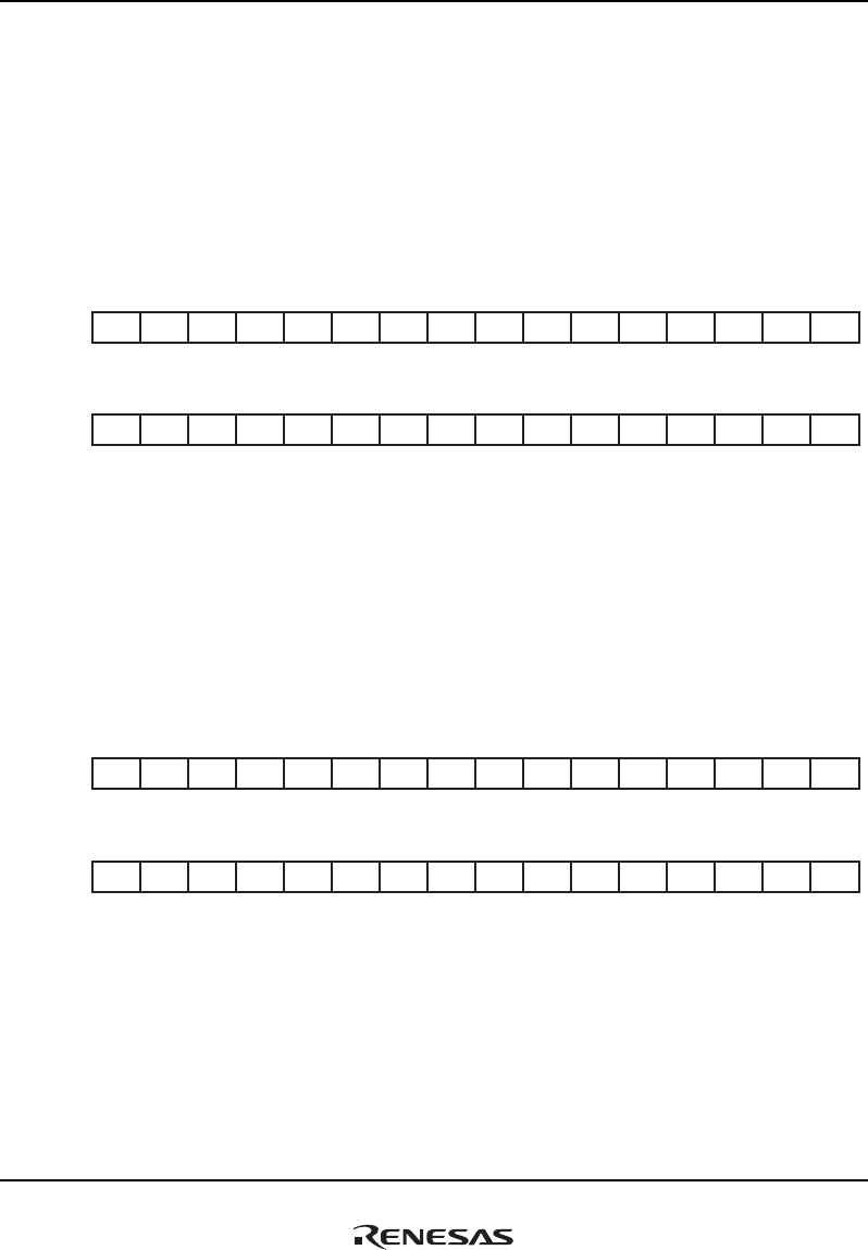
26. Serial Sound Interface (SSI) Module
Rev.1.00 Jan. 10, 2008 Page 1313 of 1658
REJ09B0261-0100
26.3.3 Transmit Data Register (SSITDR)
SSITDR is a 32-bit register that stores data to be transmitted.
Data written to SSITDR is transferred to the shift register as it is required for transmission. If the
data word length is less than 32 bits then its alignment should be as defined by the PDTA control
bit in SSICR.
Reading this register will return the data in the buffer.
31 30 29 28 27 26 25 24 23 22 21 20 19 18 17 16
000000000000000
0
Bit:
Initial value:
R/W:
Bit:
Initial value:
R/W:
15 14 13 12 11 10 9 8 7 6 5 4 3 2 1 0
R/W R/W R/W R/W R/W R/W R/W R/WR/W R/W R/W R/WR/WR/WR/W R/W
0000000000000000
R/W R/W R/W R/W R/W R/W R/W R/WR/W R/W R/W R/WR/WR/WR/W R/W
26.3.4 Receive Data Register (SSIRDR)
SSIRDR is a 32-bit register that stores the received data.
Data in SSIRDR is transferred from the shift register as each data word is received. If the data
word length is less than 32 bits then its alignment should be as defined by the PDTA control bit in
SSICR.
31 30 29 28 27 26 25 24 23 22 21 20 19 18 17 16
000000000000000
0
Bit:
Initial value:
R/W:
Bit:
Initial value:
R/W:
1514131211109876543210
RRRRR RRRRRR RRRRR
0000000000000000
RRRRR RRRRRR RRRRR

26. Serial Sound Interface (SSI) Module
Rev.1.00 Jan. 10, 2008 Page 1314 of 1658
REJ09B0261-0100
26.4 Operation
26.4.1 Bus Format
The SSI module can operate as a transmitter or a receiver and can be configured into many serial
bus formats in either mode.
The bus formats can be one of eight major modes as shown in table 26.3.
Table 26.3 Bus Formats of SSI Module
Bus Format
TPMD
CPEN
SCKD
SWSD
EN
MUEN
DIEN
IIEN
OIEN
UIEN
DEL
PDTA
SDTA
SPDP
SWSP
SCKP
SWL[2:0]
DWL[2:0]
CHNL[1:0]
Non-Compressed
Slave Receiver
0 0 0 0
Non-Compressed
Slave Transmitter
1 0 0 0
Non-Compressed
Master Receiver
0 0 1 1
Non-Compressed
Master Transmitter
1 0 1 1
Control bits Configuration bits
Compressed Slave
Receiver
0 1 0/1 0 Control bits 1 Ignored Configu-
ration
bits
Ignored
Compressed Slave
Transmitter Cannot be used
Compressed
Master Receiver
0 1 0/1 1
Compressed
Master Transmitter
1 1 0/1 1
Control bits 1 Ignored Configu-
ration
bits
Ignored

26. Serial Sound Interface (SSI) Module
Rev.1.00 Jan. 10, 2008 Page 1315 of 1658
REJ09B0261-0100
26.4.2 Non-Compressed Modes
The non-compressed mode is designed to support all serial audio streams which are split into
channels. It can support Philips, Sony and Matsushita modes as well as many more variants on
these modes.
(1) Slave Receiver
This mode allows the SSI module to receive serial data from another device. The clock and word
select signals used for the serial data stream are also supplied from an external device. If these
signals do not conform to the format as specified in the SSI module then operation is not
guaranteed.
(2) Slave Transmitter
This mode allows the SSI module to transmit serial data to another device. The clock and word
select signals used for the serial data stream are also supplied from an external device. If these
signals do not conform to the format as specified in the SSI module then operation is not
guaranteed.
(3) Master Receiver
This mode allows the SSI module to receive serial data from another device. The clock and word
select signals are internally derived from the SSI_CLK input clock. The format of these signals is
as defined in the SSI module. If the incoming data does not conform to the defined format then
operation is not guaranteed.
(4) Master Transmitter
This mode allows the SSI module to transmit serial data to another device. The clock and word
select signals are internally derived from the SSI_CLK input clock. The format of these signals is
as defined in the configuration bits in the SSI module.
(5) Configuration Fields—Word Length Related
All configuration bits relating to the word length of SSICR are valid in non-compressed modes.
There are many configurations that the SSI module can support and it is not sensible to show all of
the serial data formats in this document. Some of the combinations are shown below for the
popular formats by Philips, Sony, and Matsushita.
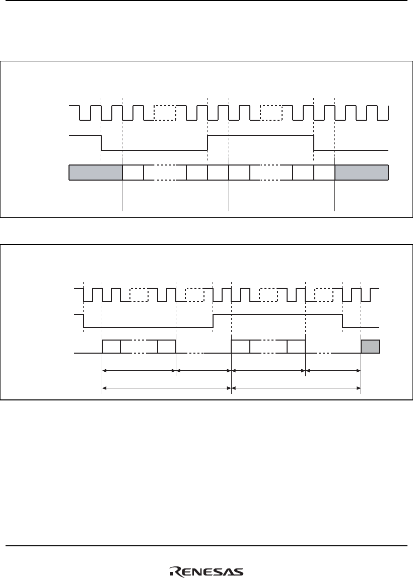
26. Serial Sound Interface (SSI) Module
Rev.1.00 Jan. 10, 2008 Page 1316 of 1658
REJ09B0261-0100
1. Philips Format
Figures 26.2 and 26.3 show the supported Philips protocol both with padding and without.
Padding occurs when the data word length is smaller than the system word length.
System word 1 =
data word 1
System word 2 =
data word 2
SCKP = 0, SWSP = 0, DEL = 0, CHNL = 00
System word length = data word length
prev. sample MSB
LSB+1
LSB MSB
LSB+1
LSB next sample
SSI_SCK
SSI_WS
SSI_SDATA
Figure 26.2 Philips Format (with No Padding)
System word 1 System word 2
Data word 1 Data word 2PaddingPadding
SCKP = 0, SWSP = 0, DEL = 0, CHNL = 00, SPDP = 0, SDTA = 0
System word length > data word length
MSB LSB MSB LSB next
SSI_SCK
SSI_WS
SSI_SDATA
Figure 26.3 Philips Format (with Padding)
Figure 26.4 shows the format used by Sony. Figure 26.5 shows the format used by Matsushita.
Padding is assumed in both cases, but may not be present in a final implementation if the
system word length equals the data word length.
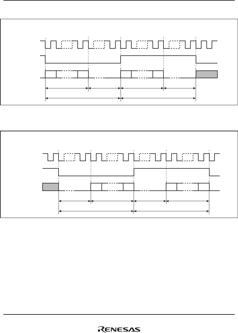
26. Serial Sound Interface (SSI) Module
Rev.1.00 Jan. 10, 2008 Page 1317 of 1658
REJ09B0261-0100
2. Sony Format
System word 1 System word 2
Data word 1 Data word 2PaddingPadding
SCKP = 0, SWSP = 0, DEL = 1, CHNL = 00, SPDP = 0, SDTA = 0
System word length > data word length
MSB LSB MSB LSB next
SSI_SCK
SSI_WS
SSI_SDATA
Figure 26.4 Sony Format (with Serial Data First, Followed by Padding Bits)
3. Matsushita Format
System word 1 System word 2
Data word 1 Data word 2PaddingPadding
SCKP = 0, SWSP = 0, DEL = 1, CHNL = 00, SPDP = 0, SDTA = 1
System word length > data word length
MSB LSB MSB LSBprev
SSI_SCK
SSI_WS
SSI_SDATA
Figure 26.5 Matsushita Format (with Padding Bits First, Followed by Serial Data)
(6) Multi-Channel Formats
There is an extend format of the definition of the specification by Philips and allows more than 2
channels to be transferred within two system words.
The SSI module supports the transfer of 4, 6 and 8 channels by the use of the CHNL, SWL and
DWL bits. It is important that the system word length (SWL) is greater than or equal to the
number of channels (CHNL) times the data word length (DWL).
Table 26.4 shows the number of padding bits for each of the valid configurations. If a setup is not
valid it does not have a number in the following table and has instead a dash.

26. Serial Sound Interface (SSI) Module
Rev.1.00 Jan. 10, 2008 Page 1318 of 1658
REJ09B0261-0100
Table 26.4 Number of Padding Bits for Each Valid Configuration
Padding Bits Per System Word DWL[2:0] 000 001 010 011 100 101 110
CHNL
[1:0]
Decoded
Channels per
System Word
SWL
[2:0]
Decoded
Word
Length 8 16 18 20 22 24 32
000 8 0 — — — — — —
001 16 8 0 — — — — —
010 24 16 8 6 4 2 0 —
011 32 24 16 14 12 10 8 0
100 48 40 32 30 28 26 24 16
101 64 56 48 46 44 42 40 32
110 128 120 112 110 108 106 104 96
00 1
111 256 248 240 238 236 234 232 224
000 8 — — — — — — —
001 16 0 — — — — — —
010 24 8 — — — — — —
011 32 16 0 — — — — —
100 48 32 16 12 8 4 0 —
101 64 48 32 28 24 20 16 0
110 128 112 96 92 88 84 80 64
01 2
111 256 240 224 220 216 212 208 192
000 8 — — — — — — —
001 16 — — — — — — —
010 24 0 — — — — — —
011 32 8 — — — — — —
100 48 24 0 — — — — —
101 64 40 16 10 4 — — —
110 128 104 80 74 68 62 56 32
10 3
111 256 232 208 202 196 190 184 160
11 4 000 8 — — — — — — —
001 16 — — — — — — —
010 24 — — — — — — —
011 32 0 — — — — — —
100 48 16 — — — — — —
101 64 32 0 — — — — —
110 128 96 64 56 48 40 32 0
111 256 224 192 184 176 168 160 128
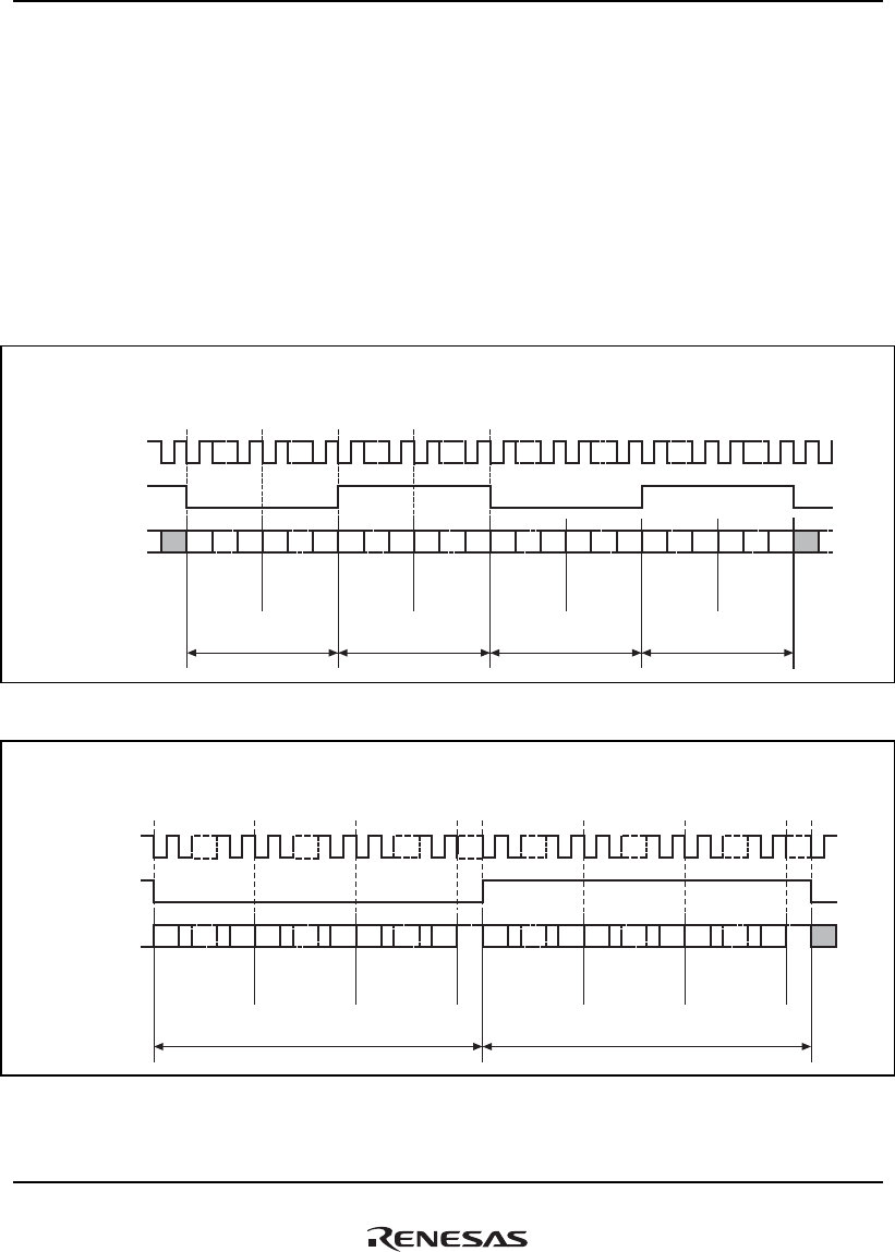
26. Serial Sound Interface (SSI) Module
Rev.1.00 Jan. 10, 2008 Page 1319 of 1658
REJ09B0261-0100
In the case of the SSI module configured as a transmitter then each word that is written to SSITDR
is transmitted in order on the serial audio bus.
In the case of the SSI module configured as a receiver each word received on the serial audio bus
is presented for reading in order by SSIRDR.
Figures 26.6 to 26.8 show how 4, 6 and 8 channels are transferred on the serial audio bus.
Note that there are no padding bits in the first example, serial data is transmitted/received first and
followed by padding bits in the second example, and padding bits are transmitted/received first
and followed by serial data in the third example. This selection is purely arbitrary.
Data
word 1
Data
word 2
Data
word 3
Data
word 4
System word 1 System word 2
Data
word 1
Data
word 2
Data
word 3
Data
word 4
System word 1 System word 2
SCKP = 0, SWSP = 0, DEL = 1, CHNL = 01, SPDP = don't care, SDTA = don't care
System word length = data word length × 2
MSB LSB MSB LSB MSB LSB MSB LSB MSB LSB MSB LSB MSB LSB MSB LSBLSB MSB
SSI_SCK
SSI_WS
SSI_SDATA
Figure 26.6 Multi-channel Format (4 Channels, No Padding)
System word 2
Data
word 1
Data
word 2
Data
word 3
Padding
System word 1
Data
word 4
Data
word 5
Data
word 6
Padding
SCKP = 0, SWSP = 0, DEL = 1, CHNL = 10, SPDP = 1, SDTA = 0
System word length = data word length × 3
MSB LSB MSB LSB MSB LSB MSBMSB LSB MSB LSB MSB LSB
SSI_SCK
SSI_WS
SSI_SDATA
Figure 26.7 Multi-channel Format (6 Channels with High Padding)
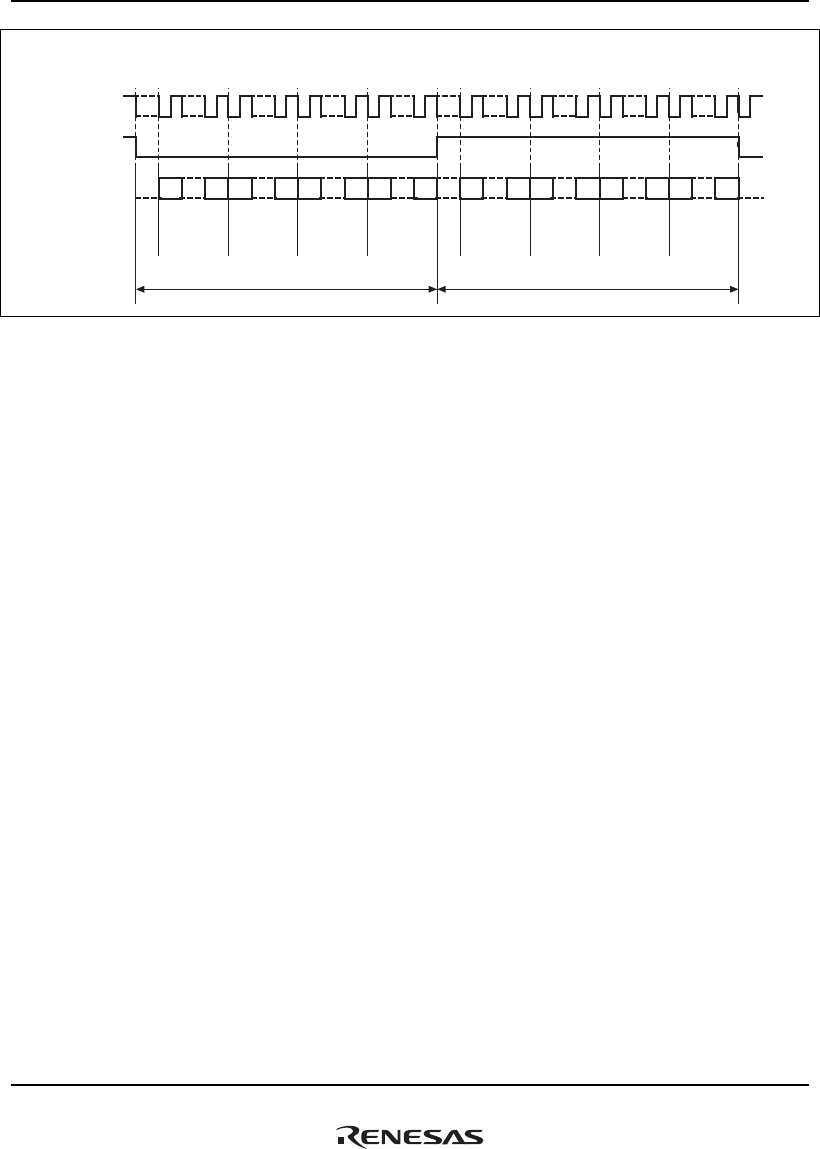
26. Serial Sound Interface (SSI) Module
Rev.1.00 Jan. 10, 2008 Page 1320 of 1658
REJ09B0261-0100
System word 2
Data
word 1
Data
word 2
Data
word 3
Data
word 4
Data
word 5
Data
word 6
Data
word 7
Data
word 8
Padding
System word 1
Padding
SCKP = 0, SWSP = 1, DEL = 1, CHNL = 11, SPDP = 0, SDTA = 1
System word length > data word length × 4
MSB LSB MSB LSB MSB LSB MSB LSB MSB LSB MSB LSB MSB LSB MSB LSB
SSI_SCK
SSI_WS
SSI_SDATA
Figure 26.8 Multi-channel Format (8 Channels,
Serial Data First, Followed by Padding Bits, with Padding)
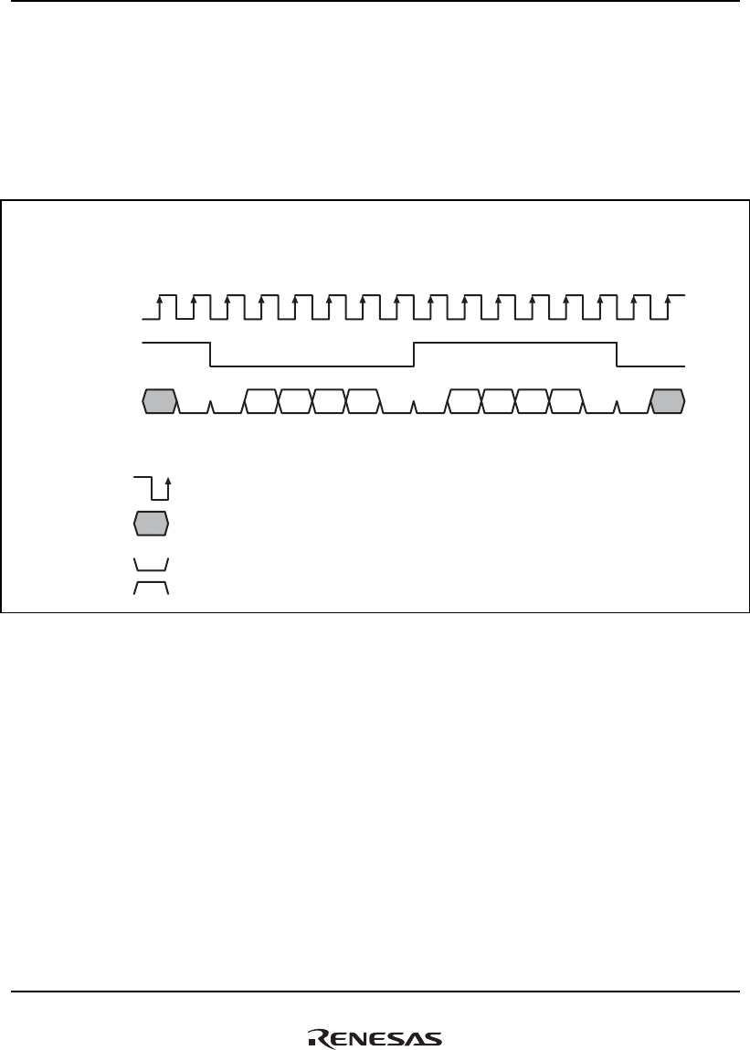
26. Serial Sound Interface (SSI) Module
Rev.1.00 Jan. 10, 2008 Page 1321 of 1658
REJ09B0261-0100
(7) Configuration Fields—Signal Format Fields
There are several more configuration bits in non-compressed mode which will now be
demonstrated. These bits are NOT mutually exclusive, however some configurations will probably
not be useful for any other device.
They are demonstrated by referring to the following basic sample format shown in figure 26.9.
Key for this and following diagrams:
means a low level on the serial bus (padding or mute)
means a high level on the serial bus (padding)
Arrow head indicates sampling point of receiver
Bit n in SSITDR
1st channel 2nd channel
SWL = 6 bits (not attainable in SSI module, demonstration only)
DWL = 4 bits (not attainable in SSI module, demonstration only)
CHNL = 00, SCKP = 0, SWSP = 0, SPDP = 0, SDTA = 0, PDATA = 0, DEL = 0, MUEN = 0
4-bit data samples continuously written to SSITDR are transmitted onto the serial audio bus.
0000 00
0
1
TDn
TD28 TD31TD31 TD30 TD29 TD28 TD31 TD30 TD29 TD28
SSI_SCK
SSI_WS
SSI_SDATA
Figure 26.9 Basic Sample Format
(Transmit Mode with Example System/Data Word Length)
In figure 26.9, system word length of 6 bits and a data word length of 4 bits are used. Neither of
these are possible with the SSI module but are used only for clarification of the other
configuration bits.

26. Serial Sound Interface (SSI) Module
Rev.1.00 Jan. 10, 2008 Page 1322 of 1658
REJ09B0261-0100
1. Inverted Clock
System word 1 System word 2
As basic sample format configuration except SCKP = 1
SSI_SCK
SSI_WS
SSI_SDATA
0000 00TD28 TD31TD31 TD30 TD29 TD28 TD31 TD30 TD29 TD28
Figure 26.10 Inverted Clock
2. Inverted Word Select
System word 1 System word 2
As basic sample format configuration except SWSP = 1
0000 00TD28 TD31TD31 TD30 TD29 TD28 TD31 TD30 TD29 TD28
SSI_SCK
SSI_WS
SSI_SDATA
Figure 26.11 Inverted Word Select
3. Inverted Padding Polarity
System word 1 System word 2
As basic sample format configuration except SPDP = 1
TD28 TD311 1 1 1 1 1TD31 TD30 TD29 TD28 TD31 TD30 TD29 TD28
SSI_SCK
SSI_WS
SSI_SDATA
Figure 26.12 Inverted Padding Polarity
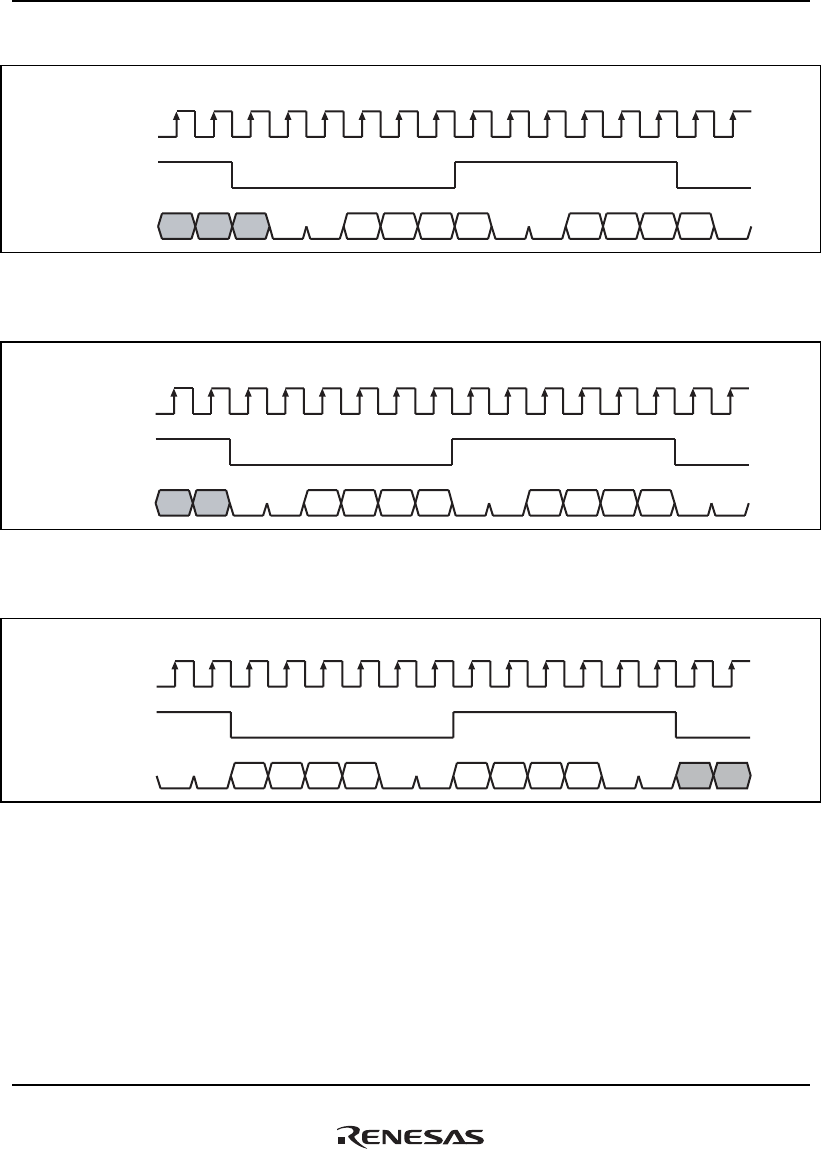
26. Serial Sound Interface (SSI) Module
Rev.1.00 Jan. 10, 2008 Page 1323 of 1658
REJ09B0261-0100
4. Padding Bits First, Followed by Serial Data, with Delay
System word 1 System word 2
As basic sample format configuration except SDTA = 1
000TD28 0 0TD30 TD29 TD31 TD30 TD29 TD28 TD31 TD30 TD29 TD28
SSI_SCK
SSI_WS
SSI_SDATA
Figure 26.13 Padding Bits First, Followed by Serial Data, with Delay
5. Padding Bits First, Followed by Serial Data, without Delay
As basic sample format configuration except SDTA = 1 and DEL = 1
System word 1 System word 2
000TD28 0 0TD29 0TD31 TD30 TD29 TD28 TD31 TD30 TD29 TD28
SSI_SCK
SSI_WS
SSI_SDATA
Figure 26.14 Padding Bits First, Followed by Serial Data, without Delay
6. Serial Data First, Followed by Padding Bits, without Delay
As basic sample format configuration except DEL = 1
System word 1 System word 2
0000 00TD31 TD30TD31 TD30 TD29 TD28 TD31 TD30 TD29 TD28
SSI_SCK
SSI_WS
SSI_SDATA
Figure 26.15 Serial Data First, Followed by Padding Bits, without Delay
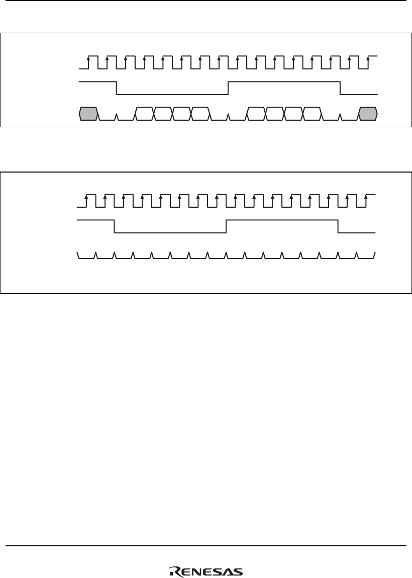
26. Serial Sound Interface (SSI) Module
Rev.1.00 Jan. 10, 2008 Page 1324 of 1658
REJ09B0261-0100
7. Parallel Right Aligned with Delay
As basic sample format configuration except PDTA = 1
System word 1 System word 2
0000 00TD3TD0 TD3 TD2 TD1 TD0 TD3 TD2 TD1 TD0
SSI_SCK
SSI_WS
SSI_SDATA
Figure 26.16 Parallel Right Aligned with Delay
8. Mute Enabled
As basic sample format configuration except MUEN = 1 (TD data ignored)
System word 1 System word 2
0 0000 0 000000 000 0
When MUBN = 1 in transmit mode, a low level is output from the SSI_SDATA pin regardless of padding setting.
SSI_SCK
SSI_WS
SSI_SDATA
Figure 26.17 Mute Enabled
26.4.3 Compressed Modes
The compressed mode is used to transfer a continuous bit stream. This would typically be a
compressed bit stream which requires downstream decoding.
When burst mode is not enabled, there is no concept of a data word. However in order to receive
and transmit it is necessary to transfer between the serial bus and word formatted memory.
Therefore the word boundary selection is arbitrary during receive/transmit and must be dealt with
by another module. When burst mode is enabled then data bits being transmitted can be identified
by virtue of the fact that the serial clock output is only activated when there is a word to be output
and only the required number of clock pulses necessary to clock out each 32-bit word are
generated. The serial bit clock stops at a low level when SSICR.SCKP = 0, and at a high level
when SSICR.SCKP = 1. Note burst mode is only valid in the context of the SSI module being a
transmitter of data. Burst mode data cannot be received by this module.
Data is transmitted and received in blocks of 32 bits, and the first bit received/transmitted bit is bit
31 when stored in memory.
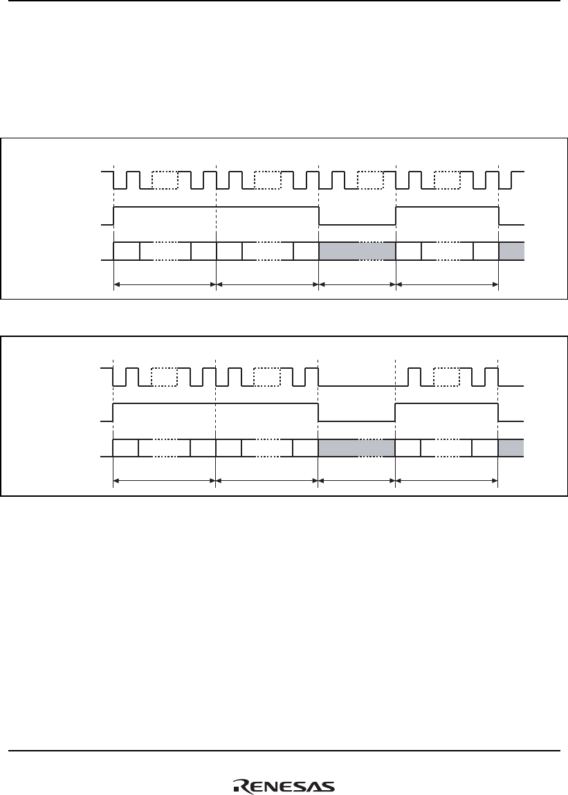
26. Serial Sound Interface (SSI) Module
Rev.1.00 Jan. 10, 2008 Page 1325 of 1658
REJ09B0261-0100
The word select pin in this mode does not act as a system word start signal as in non-compressed
mode, but instead is used to indicate that the receiver can receive another data burst, or the
transmitter can transmit another data burst.
Figures 26.18 and 26.19 show the compressed mode data transfer, with burst mode disabled, and
enabled, respectively.
TRMD = 1, CPEN = 1, SCKD = 1, SWSD = 1, SWSP = 0, BREN = 0
Data word 1 Data word 2 Data word 3Null data
MSB LSB MSB LSBMSB LSB
SSI_SCK
SSI_WS
SSI_SDATA
Figure 26.18 Compressed Data Format, Master Transmitter, Burst Mode Disabled
TRMD = 1, CPEN = 1, SCKD = 1, SWSD = 1, SWSP = 0, BREN = 1
Data word 1 Data word 2 Data word 3Null data
MSB LSB MSB LSBMSB LSB
SSI_SCK
SSI_WS
SSI_SDATA
Figure 26.19 Compressed Data Format, Master Transmitter, and Burst Mode Enabled

26. Serial Sound Interface (SSI) Module
Rev.1.00 Jan. 10, 2008 Page 1326 of 1658
REJ09B0261-0100
(1) Slave Receiver
This mode allows the module to receive a serial bit stream from another device and store it in
memory.
The shift register clock can be supplied from an external device or from an internal clock.
The word select pin is used as an input flow control. Assuming that SWSP = 0 if SSI_WS is high
then the module will receive the bit stream in blocks of 32 bits, one data bit per clock. If SSI_WS
goes low then the module will complete the current 32-bit block and then stop any further
reception, until SSI_WS goes high again.
(2) Slave Transmitter
This mode cannot be used.
(3) Master Receiver
This mode allows the SSI module to receive a serial bit stream from another device and store it in
memory.
The shift register clock can be supplied from an external device or from an internal clock.
The word select pin is used as an output flow control. The module always asserts the word select
signal to indicate it can receive more data continuously. It is the responsibility of the transmitting
device to ensure it can transmit data to the SSI module in time to ensure no data is lost.
(4) Master Transmitter
This mode allows the module to transmit a serial bit stream from internal memory to another
device.
The shift register clock can be supplied from an external device or from an internal clock.
The word select pin is used as an output flow control. The module always asserts the word select
signal to indicate it will transmit more data continuously. Word select signal is not asserted until
the first word is ready to transmit however. It is the responsibility of the receiving device to ensure
it can receive the serial data in time to ensure no data is lost.
When the configuration for data transfer is completed, the SSI module can work with the
minimum interaction with CPU. The CPU specifies settings for the SSI module and DMAC then
handles overflow/ underflow interrupts if required.

26. Serial Sound Interface (SSI) Module
Rev.1.00 Jan. 10, 2008 Page 1327 of 1658
REJ09B0261-0100
26.4.4 Operation Modes
There are three modes of operation: configuration, enabled and disabled. Figure 26.20 shows the
transition diagram between these operation modes.
EN = 1
(IDST = 0)
EN = 0
(IDST = 0)
EN = 0
(IDST = 1)
Module
configration
(after reset)
Module
enabled
(normal tx/rx)
Module
disabled
(waiting until
bus inactive)
Power-on reset
Manual reset
Figure 26.20 Transition Diagram between Operation Modes
(1) Configuration Mode
This mode is entered after the module is released from reset. All required settings in the control
register should be defined in this mode, before the SSI module is enabled by setting the EN bit.
Setting the EN bit causes the SSI module to enter the module enabled mode.
(2) Module Enabled Mode:
Operation of the module in this mode depends on the selected operating mode. For details, see
section 26.4.5, Transmit Operation and section 26.4.6, Receive Operation.

26. Serial Sound Interface (SSI) Module
Rev.1.00 Jan. 10, 2008 Page 1328 of 1658
REJ09B0261-0100
26.4.5 Transmit Operation
Transmission can be controlled in one of two ways: either DMA or an interrupt driven.
DMA driven is preferred to reduce the CPU load. In DMA control mode, an underflow or
overflow of data or DMAC transfer end is notified by using an interrupt.
The alternative is using the interrupts that the SSI module generates to supply data as required.
This mode has a higher interrupt load as the SSI module is only double buffered and will require
data to be written at least every system word period.
When disabling the SSI module, the SSI clock* must be supplied continuously until the module
enters in the idle state, indicated by the IIRQ bit.
Figure 26.21 shows the transmit operation in the DMA controller mode. Figure 26.22 shows the
transmit operation in the interrupt controller mode.
Note: * SCKD = 0: Clock input through the SSI_SCK pin
SCKD = 1: Clock input through the SSI_CLK pin
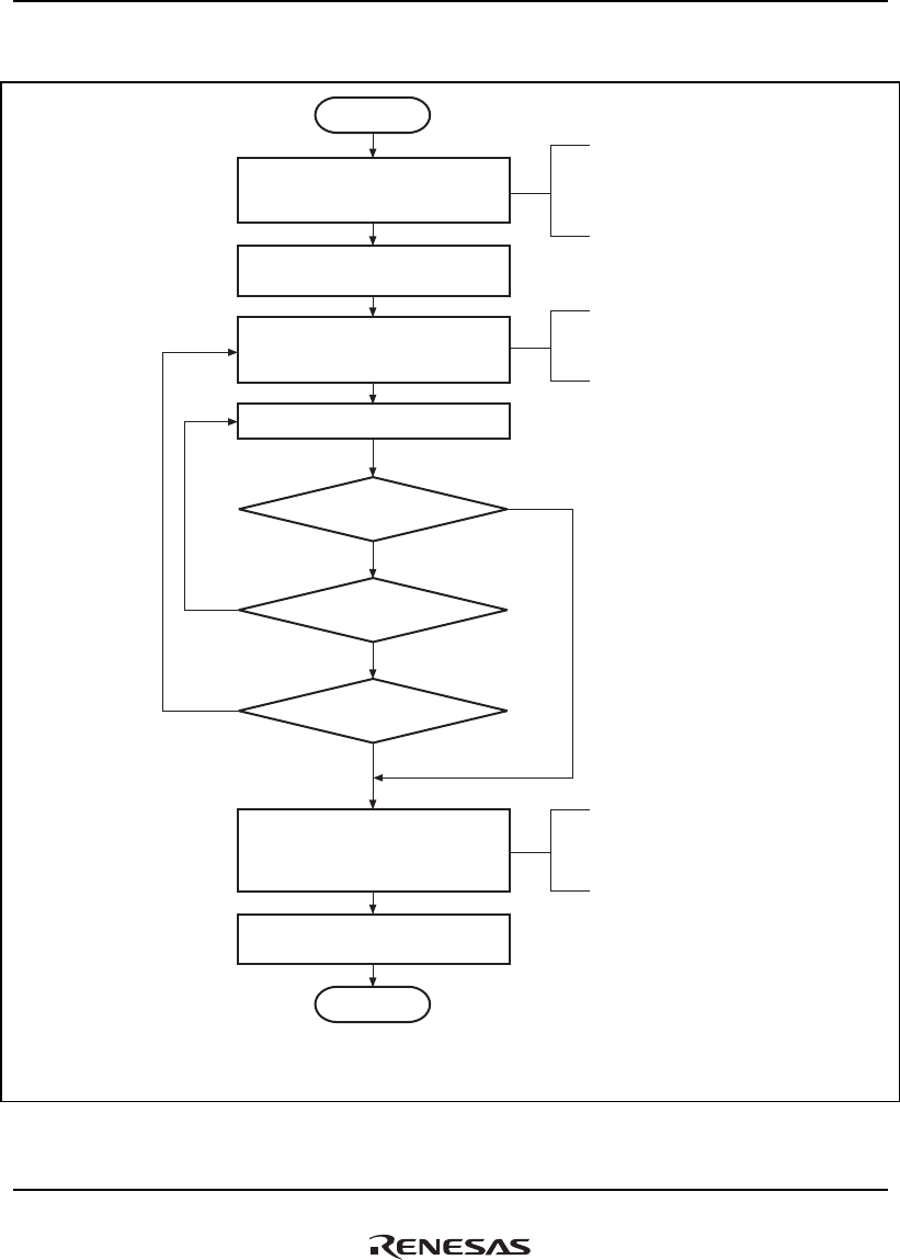
26. Serial Sound Interface (SSI) Module
Rev.1.00 Jan. 10, 2008 Page 1329 of 1658
REJ09B0261-0100
(1) Transmission Using DMA Controller
No
Yes
Yes
Start
End*
Release reset,
specify configuration bits
in SSICR
Setup DMA controller to provide data
as required for transmission
Wait for interrupt from DMAC or SSI
Enable SSI module,
enable DMA,
enable error interrupts
Disable SSI module,
disable DMA
disable error interrupt,
enable Idle interrupt
Note: * When SSI error interrupt occurs (underflow/overflow), back to start
and execute flow again.
EN = 0,
DMEN = 0
UIEN = 0, OIEN = 0,
IIEN = 1
Wait for idle interrupt
from SSI module
SSI
error interrupt?
Has DMAC
Tx data been
completed?
More data to be send?
EN = 1,
DMEN = 1,
UIEN = 1, OIEN = 1
Specify TRMD, EN, SCKD,
SWSD, MUEN, DEL, PDTA,
SDTA, SPDP, SWSP, SCKP,
SWL, DWL, CHNL
Figure 26.21 Transmission Using DMA Controller
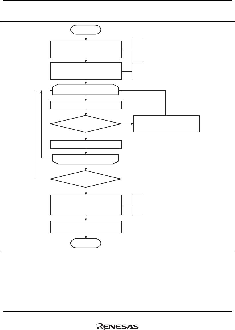
26. Serial Sound Interface (SSI) Module
Rev.1.00 Jan. 10, 2008 Page 1330 of 1658
REJ09B0261-0100
(2) Transmission using Interrupt Data Flow Control
Start
End
Release reset,
specify configuration bits
in SSICR
Enable SSI module,
enable DMA,
enable error interrupts
Wait for Idle interrupt
from SSI module
Disable SSI module,
disable DMA
disable error interrupt,
enable Idle interrupt
Wait for interrupt from SSI
Use SSI status register bits
to realign data
after underflow/overflow
Load data of channel n
n = ( (CHNL + 1) x 2)
Loop
Next Channel
Data interrupt?
More data
to be send?
Specify TRMD, EN, SCKD,
SWSD, MUEN, DEL, PDTA,
SDTA, SPDP, SWSP, SCKP,
SWL, DWL, CHNL
EN = 1,
DIEN = 1,
UIEN = 1, OIEN = 1
EN = 0,
DIEN = 0
UIEN = 0, OIEN = 0,
IIEN = 1
No
No
Yes
Yes
Figure 26.22 Transmission Using Interrupt Data Flow Control

26. Serial Sound Interface (SSI) Module
Rev.1.00 Jan. 10, 2008 Page 1331 of 1658
REJ09B0261-0100
26.4.6 Receive Operation
As with transmission the reception can be controlled in one of two ways: either DMA or an
interrupt driven.
Figures 26.23 and 26.24 show the flow of operation.
When disabling the SSI module, the SSI clock must be supplied continuously until the module
enters in the idle state, which is indicated by the IIRQ bit.
Note: * SCKD = 0: Clock input through the SSI_SCK pin
SCKD = 1: Clock input through the SSI_CLK pin
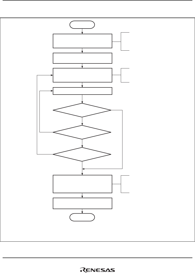
26. Serial Sound Interface (SSI) Module
Rev.1.00 Jan. 10, 2008 Page 1332 of 1658
REJ09B0261-0100
(1) Reception Using DMA Controller
Start
End*
Release reset,
specify configuration bits
in SSICR
Setup DMA controller to transfer data
from SSI module to memory
Wait for interrupt from DMAC or SSI
Enable SSI module,
enable DMA,
enable error interrupts
Wait for idle interrupt
from SSI module
Disable SSI module,
disable DMA
disable error interrupt,
enable Idle interrupt
SSI
Error interrupt?
Has DMAC Rx data
been completed?
More data
to be received?
Specify TRMD, EN, SCKD,
SWSD, MUEN, DEL, PDTA,
SDTA, SPDP, SWSP, SCKP,
SWL, DWL, CHNL
Note: * When SSI error interrupt occurs (underflow/overflow), back to start
and execute flow again.
EN = 0,
DMEN = 0
UIEN = 0, OIEN = 0,
IIEN = 1
EN = 1,
DMEN = 1,
UIEN = 1, OIEN = 1
Yes
Yes
No
No
No
Yes
Figure 26.23 Reception Using DMA Controller
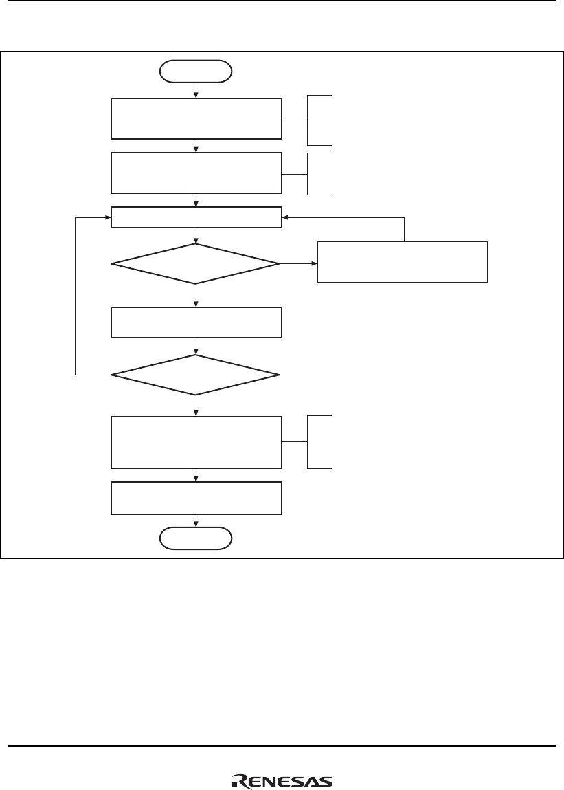
26. Serial Sound Interface (SSI) Module
Rev.1.00 Jan. 10, 2008 Page 1333 of 1658
REJ09B0261-0100
(2) Reception Using Interrupt Data Flow Control
Start
End
Release reset,
specify configuration bits
in SSICR
Read data from
receive data register
Wait for interrupt from SSI
Enable SSI module,
enable data interrupt,
enable error interrupts
Use SSI status register bits
to realign data
after underflow/overflow
Wait for idle interrupt
from SSI module
Disable SSI module,
disable data interrupt
disable error IRQ,
enable idle IRQ
SSI
Error interrupt?
More data to be
received?
Specify TRMD, EN, SCKD,
SWSD, MUEN, DEL, PDTA,
SDTA, SPDP, SWSP, SCKP,
SWL, DWL, CHNL
EN = 0,
DIEN = 0
UIEN = 0, OIEN = 0,
IIEN = 1
EN = 1,
DIEN = 1,
UIEN = 1, OIEN = 1
Yes
Yes
No
No
Figure 26.24 Reception Using Interrupt Data Flow Control

26. Serial Sound Interface (SSI) Module
Rev.1.00 Jan. 10, 2008 Page 1334 of 1658
REJ09B0261-0100
When an underflow or overflow error condition is met (UIRQ = 1 or OIRQ = 1), the CHNO[1:0]
and SWNO bits can be used to recover the SSI module to a known status. When an underflow or
overflow occurs, the CPU can read the number of channels and the number of system words to
determine what point the serial audio stream has currently reached. In the transmitter case, the
CPU can skip forward through the data it wants to transmit until the transmit of the data for which
the SSI module is expecting to transmit next is enabled, and so resynchronize with the audio data
stream. In the receiver case, the CPU can skip forward storing null sample data until it is ready to
store the sample data that the SSI module will receive next to ensure consistency of the number of
received data, and so resynchronize with the audio data stream.
26.4.7 Serial Clock Control
This function is used to control and select which clock is used for the serial bus interface.
If the serial clock direction is set to input (SCKD = 0), the SSI module is in clock slave mode, then
the bit clock that is used in the shift register is derived from the SSI_SCK pin.
If the serial clock direction is set to output (SCKD = 1), the SSI module is in clock master mode,
and the shift register uses the bit clock derived from the SSI_CLK input pin or its clock divided.
This input clock is then divided by the ratio in the serial oversampling clock division ratio
(CKDV) bits in SSICR and used as the bit clock in the shift register.
In either case, the SSI_SCK pin output is the same as the bit clock.

26. Serial Sound Interface (SSI) Module
Rev.1.00 Jan. 10, 2008 Page 1335 of 1658
REJ09B0261-0100
26.5 Usage Note
26.5.1 Restrictions when an Overflow Occurs during Receive DMA Operation
If an overflow occurs during receive DMA operation, the module must be reactivated.
The receive buffer of SSI has 32-bit common register to the left channel and right channel. If an
overflow occurs under the condition of control register (SSICR) data-word length (DWL2 to 0) is
32-bit and system-word length (SWL2 to 0) is 32-bit, SSI has received the data at right channel
that should be received at left channel.
If an overflow occurrence is confirmed through an overflow error interrupt or overflow error status
flag (the OIRQ bit in SSISR), disable the DMA transfer of the SSI to halt its operation by writing
0 to the EN bit and DMEN bit in SSICR (then terminate the DMAC setting). And clear the
overflow status flag by writing 0 to the OIRQ bit, set the DMA again to restart transfer.
26.5.2 Pin Function Setting for the SSI Module
Before setting or activating the SSI module, set the peripheral module select registers and the port
control registers in terms of the SSI0 and SSI1 channels as described in section 28, General
Purpose I/O Ports (GPIO).
26.5.3 Usage Note in Slave Mode
When terminating data transmission in slave mode, the WS signal (SSI WS) input should be kept
the active state until SSICR.IDST becomes 1 after SSICR.EN is cleared to 0 (see next page
figure). The “active state” means the WS signal is being input high (or low) and low (or high)
alternately as for each system word cycles (it will become more than five system word cycles after
EN bit is cleared to 0).
If the WS signal active state input is stopped before SSICR.IDST becomes 1, the transfer of the
SSI is not terminated normally and the transfer will be suspended. If SSICR.EN is set to 1 again in
this state, the transfer is resumed from the suspended state and an unexpected data transfer may
occur.
Note that, the normal data transmission of the SSI can be resumed from the first or second WS
falling edge after the EN bit is set to 1 while the IDST bit is 1.
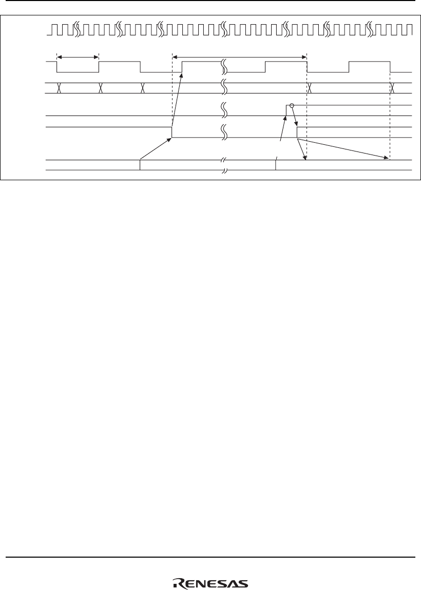
26. Serial Sound Interface (SSI) Module
Rev.1.00 Jan. 10, 2008 Page 1336 of 1658
REJ09B0261-0100
SCK
SSI_WS
SSI_SDATA
SSISR.IDST
SSICR.EN
Data transmission
One system word
Idle or data transmission
SSI internal
state
Keep active WS input until IDST become 1
(more than five system words)
Resumption from first or second WS falling
edge (SWSP = 0) after EN bit is set to 1
Termination and transition to idle
Figure 26.25 SSI Transfer Termination and Resumption Timing in Slave Mode

27. NAND Flash Memory Controller (FLCTL)
Rev.1.00 Jan. 10, 2008 Page 1337 of 1658
REJ09B0261-0100
Section 27 NAND Flash Memory Controller (FLCTL)
The NAND flash memory controller (FLCTL) provides interfaces with an external NAND-type
flash memory.
27.1 Features
(1) NAND-Type Flash Memory Interface
• Interface that can be connected to NAND-type flash memory
• Read or write in sector* units (512 + 16 bytes)
• Read or write in byte units
Note: * In the data sheet of NAND-type flash memory, an access unit of some products is
defined to be 2048 + 64 bytes as a page. In this document, a sector always refers to the
access unit of 512 + 16 bytes.
(2) Access Modes
The FLCTL has two selectable access modes.
• Command access mode:
Performs an access by specifying a command to be issued from the FLCTL to flash memory,
address, and data size to be input or output.
• Sector access mode:
Read or write in physical sector units by specifying a physical sector. By specifying the
number of sectors, the continuous physical sectors can be read from or written to.
(3) Sectors and Control Codes
• A sector is comprised of 512-byte data and 16-byte control code.
(4) Data Error
• When a program error or erase error occurs, the error is reflected on the error source flags.
Interrupts for each source can be specified.

27. NAND Flash Memory Controller (FLCTL)
Rev.1.00 Jan. 10, 2008 Page 1338 of 1658
REJ09B0261-0100
(5) Data Transfer FIFO
• On-chip 224-byte FLDTFIFO for data transfer of flash memory
• On-chip 32-byte FLECFIFO for data transfer of a control code
• Flag bit for detection of overrun or underrun during access from the CPU or DMA
(6) DMA Transfer
• By individually specifying the transfer destinations of data and control code of flash memory
to the DMA controller, data and control code can be transferred to different areas.
(7) Access Size
• Registers include 32-bit registers and an 8-bit register. Read from or write to the register with
the specified access size.
• The access size of FIFO is 32 bits (4 bytes). In reading, set the byte number to a multiple of
four. In writing, set the byte number to a multiple of four in writing.
(8) Access Time
• The operating frequency of the FLCTL pins can be specified by the FCKSEL bit and the
QTSEL bit in FLCMNCR, regardless of the operating frequency of the peripheral bus.
• The operating clock, FCLK, on the pins for the NAND-type flash memory is used by dividing
the operating clock of the peripheral bus (a peripheral clock).
• In NAND-type flash memory, the FRE and FWE pins operate with the FCLK specified by
FLCMNCR. To ensure the setup time, this operating frequencies should not exceed the
maximum operating frequency of memory to be connected.
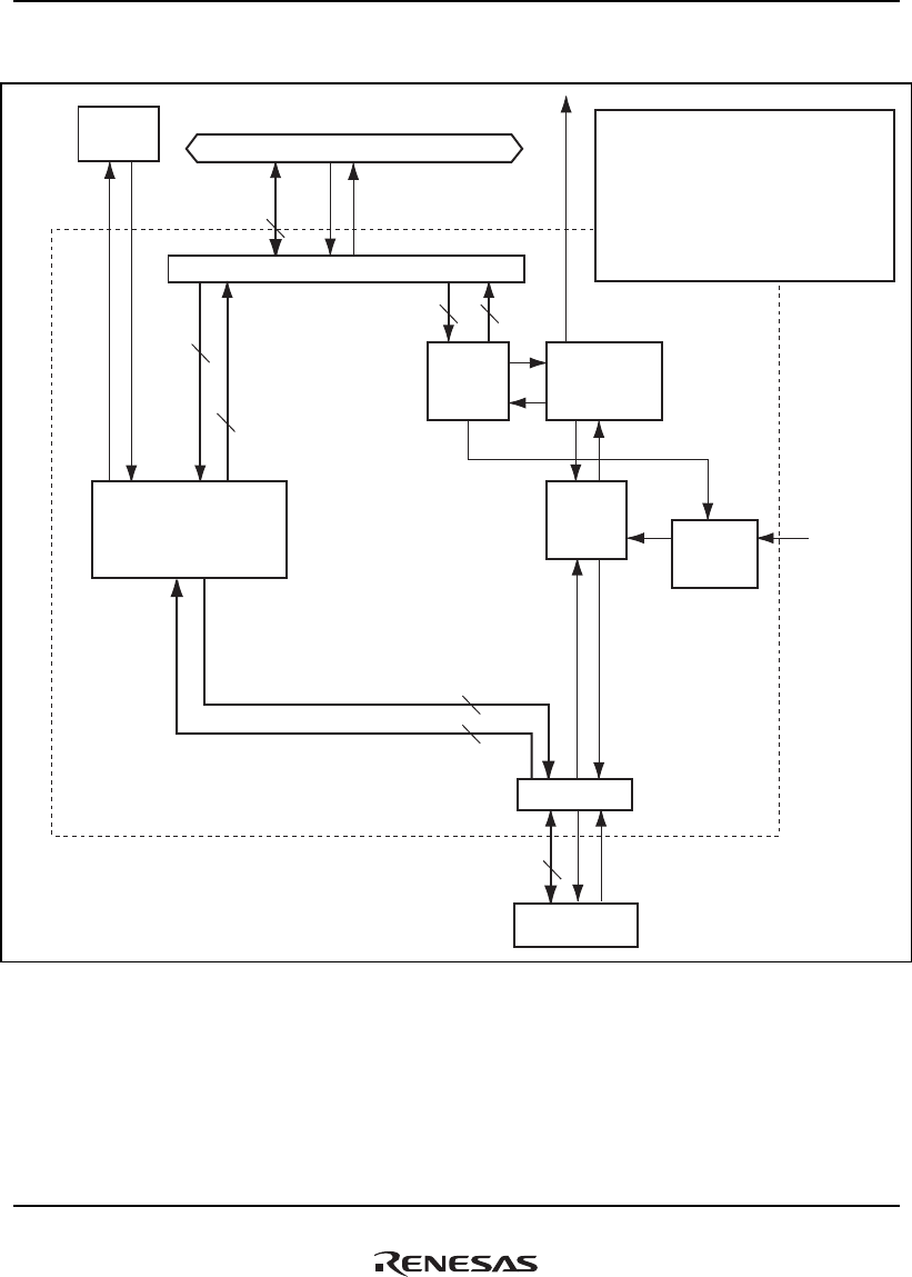
27. NAND Flash Memory Controller (FLCTL)
Rev.1.00 Jan. 10, 2008 Page 1339 of 1658
REJ09B0261-0100
Figure 27.1 shows a block diagram of the FLCTL.
DMAC
32
32
Flash interface
32
8
8
8
32 32
FLCTL
FCLK
QTSEL
FCKSEL
FLSTE (status error or ready busy
timeout error)
FLTEND (transfer end)
FLTRQ0 (FIFO0 transfer request)
FLTRQ1 (FIFO1 transfer request)
NAND-type
flash memory
FIFO
256 bytes ×1, ×1/2,
×1/4
DMA transfer
requests
(2 lines)
Peripheral bus
Peripheral bus interface
Registers Interrupt
control
Transmission/
reception
control
Control signal
Peripheral clock
Pck
•
•
•
•
Details of interrupt source
Figure 27.1 Block Diagram of FLCTL

27. NAND Flash Memory Controller (FLCTL)
Rev.1.00 Jan. 10, 2008 Page 1340 of 1658
REJ09B0261-0100
27.2 Input/Output Pins
Table 27.1 shows the pin configuration of the FLCTL.
Table 27.1 Pin Configuration
Corresponding
Flash Memory
Pin
Pin Name Function I/O NAND Type Description
FCE Chip enable Output CE Enables flash memory connected to this
LSI.
Multiplexed with SCIF0_CTS/INTD.
FD7 to
FD0
Data I/O I/O I/O7 to I/O0 I/O pins for command, address, and data.
Multiplexed with MODE3/IRL7,
MODE2/IRL6, MODE1/IRL5,
MODE0/IRL4, MODE11/SCIF4_SCK,
MODE10/SCIF4_RXD,
MODE9/SCIF4_TXD, and
MODE8/SCIF3_SCK.
FCLE Command latch
enable
Output CLE Command Latch Enable (CLE)
Asserted when a command is output.
Multiplexed with MODE4/SCIF3_TXD.
FALE Address latch
enable
Output ALE Address Latch Enable (ALE)
Asserted when an address is output.
Negated when data is input or output.
Multiplexed with MODE7/SCIF3_RXD.
FRE Read enable Output RE Read Enable (RE)
Reads data at the falling edge of RE.
Multiplexed with SCIF0_SCK/HSPI_CLK.
FWE Write enable Output WE Write Enable
Flash memory latches a command,
address, and data at the rising edge of
WE.
Multiplexed with
SCIF0_TXD/HSPI_TX/MODE8.

27. NAND Flash Memory Controller (FLCTL)
Rev.1.00 Jan. 10, 2008 Page 1341 of 1658
REJ09B0261-0100
Corresponding
Flash Memory
Pin
Pin Name Function I/O NAND Type Description
FR/B Ready/busy Input R/B Ready/Busy
Indicates ready state at high level.
Indicates busy state at low level.
Multiplexed with SCIF0_RXD/HSPI_RX.
—* — — WP Write Protect/Reset
Prevents accidental erasure or
programming when power is turned on or
off, at low level.
FSE Spare area
enable
Output SE Spare Area Enable
Enables access to spare area. This pin
must be fixed low in sector access mode.
Multiplexed with SCIF0_RTS/HSPI_CS.
Note: ∗ Not supported by this LSI.

27. NAND Flash Memory Controller (FLCTL)
Rev.1.00 Jan. 10, 2008 Page 1342 of 1658
REJ09B0261-0100
27.3 Register Descriptions
Table 27.2 shows the register configuration of FLCTL. Table 27.3 shows the register states in
each processing mode.
Table 27.2 Register Configuration of FLCTL
Register Name Abbreviation R/W P4 Address Area 7 Address
Access
Size
Sync
Clock
Common control register FLCMNCR R/W H'FFE9 0000 H'1FE9 0000 32 Pck
Command control register FLCMDCR R/W H'FFE9 0004 H'1FE9 0004 32 Pck
Command code register FLCMCDR R/W H'FFE9 0008 H'1FE9 0008 32 Pck
Address register FLADR R/W H'FFE9 000C H'1FE9 000C 32 Pck
Data register FLDATAR R/W H'FFE9 0010 H'1FE9 0010 32 Pck
Data counter register FLDTCNTR R/W H'FFE9 0014 H'1FE9 0014 32 Pck
Interrupt DMA control register FLINTDMACR R/W H'FFE9 0018 H'1FE9 0018 32 Pck
Ready busy timeout setting
register
FLBSYTMR R/W H'FFE9 001C H'1FE9 001C 32 Pck
Ready busy timeout counter FLBSYCNT R H'FFE9 0020 H'1FE9 0020 32 Pck
Data FIFO register FLDTFIFO R/W H'FFE9 0024 H'1FE9 0024 32 Pck
Control code FIFO register FLECFIFO R/W H'FFE9 0028 H'1FE9 0028 32 Pck
Transfer control register FLTRCR R/W H'FFE9 002C H'1FE9 002C 8 Pck
Address register 2 FLADR2 R/W H'FFE9 003C H'1FE9 003C 32 Pck

27. NAND Flash Memory Controller (FLCTL)
Rev.1.00 Jan. 10, 2008 Page 1343 of 1658
REJ09B0261-0100
Table 27.3 Register States in Each Processing Mode
Register Abbreviation Power-On Reset Manual Reset Sleep/Deep Sleep Module Standby
FLCMNCR H'0000 0000 H'0000 0000 Retained Retained
FLCMDCR H'0000 0000 H'0000 0000 Retained Retained
FLCMCDR H'0000 0000 H'0000 0000 Retained Retained
FLADR H'0000 0000 H'0000 0000 Retained Retained
FLDATAR H'0000 0000 H'0000 0000 Retained Retained
FLDTCNTR H'0000 0000 H'0000 0000 Retained Retained
FLINTDMACR H'0000 0000 H'0000 0000 Retained Retained
FLBSYTMR H'0000 0000 H'0000 0000 Retained Retained
FLBSYCNT H'0000 0000 H'0000 0000 Retained Retained
FLDTFIFO Undefined Undefined Retained Retained
FLECFIFO Undefined Undefined Retained Retained
FLTRCR H'00 H'00 Retained Retained
FLADR2 H'0000 0000 H'0000 0000 Retained Retained

27. NAND Flash Memory Controller (FLCTL)
Rev.1.00 Jan. 10, 2008 Page 1344 of 1658
REJ09B0261-0100
27.3.1 Common Control Register (FLCMNCR)
FLCMNCR is a 32-bit readable/writable register that specifies the type (NAND) of flash memory,
access mode, and FCE pin output.
31 30 29 28 27 26 25 24 23 22 21 20 19 18 17 16
15 14 13 12 11 10 9 8 7 6 5 4 3 2 1 0
0000000000000000
RRRRRRRRRRRRRR/WR/WR
0000000000000000
R/W R R R R/W R/W R/W R R R R R R/W R R R/W
Bit:
Initial value:
R/W:
Bit:
Initial value:
R/W:
QTSELSNAND
FCK
SEL ACM[1:0]
NAND
WF
CE0
TYPE
SEL
Bit Bit Name
Initial
Value R/W Description
31 to 19 — All 0 R Reserved
These bits are always read as 0. The write value should
always be 0.
18 SNAND 0 R/W Large Capacity NAND Flash Memory Select
This bit is used to specify the NAND flash memory that
a page consists of 2048 + 64 bytes.
0: Selects the flash memory that a page consists of 512
+ 16 bytes
1: Selects the flash memory that a page consists of
2048 + 64 bytes
17 QTSEL 0 R/W Quarter Flash Clock Select
0: Uses the FCLK selected by the FCKSEL bit
1: Divides the operating clock of the FLCTL (a
peripheral clock) by four and uses it as the FCLK
when FCKSEL = 0
Note: When FCKSEL = 1, setting this bit to 1 is
prohibited.
16 — 0 R Reserved
This bit is always read as 0. The write value should
always be 0.

27. NAND Flash Memory Controller (FLCTL)
Rev.1.00 Jan. 10, 2008 Page 1345 of 1658
REJ09B0261-0100
Bit Bit Name
Initial
Value R/W Description
15 FCKSEL 0 R/W Flash Clock Select
0: Divides the operating clock of the FLCTL (a
peripheral clock) by two and uses it as the FCLK
1: Uses the operating clock of the FLCTL (a peripheral
clock) as the FCLK
14 to 12 — All 0 R Reserved
These bits are always read as 0. The write value should
always be 0.
11, 10 ACM[1:0] 00 R/W Access Mode Specification [1:0]
Specify access mode.
00: Command access mode
01: Sector access mode
10: Setting prohibited
11: Setting prohibited
9 NANDWF 0 R/W NAND Wait Insertion Operation
0: No wait
1: A wait cycle is inserted
8 to 4 — All 0 R Reserved
These bits are always read as 0. The write value should
always be 0.
3 CE0 0 R/W Chip Enable 0
0: Disabled (Outputs high level to the FCE pin)
1: Enabled (Outputs low level to the FCE pin)
2, 1 — All 0 R Reserved
These bits are always read as 0. The write value should
always be 0.
0 TYPESEL 0 R/W Memory Select
0: Reserved
1: NAND-type flash memory is selected
Note: Set TYPESEL to 1 to use FLCTL.

27. NAND Flash Memory Controller (FLCTL)
Rev.1.00 Jan. 10, 2008 Page 1346 of 1658
REJ09B0261-0100
27.3.2 Command Control Register (FLCMDCR)
FLCMDCR is a 32-bit readable/writable register that issues a command in command access mode,
specifies address issue, and specifies destination of data to be input or output. In sector access
mode, FLCMDCR specifies the number of sector transfers.
31 30 29 28 27 26 25 24 23 22 21 20 19 18 17 16
1514131211109876543210
0000000000000000
R/W R/W R/W R/W R/W R/W R/W R/W R R R/W R/W R/W R/W R/W R/W
0000000000000000
R/W R/W R/W R/W R/W R/W R/W R/W R/W R/W R/W R/W R/W R/W R/W R/W
Bit:
Initial value:
R/W:
Bit:
Initial value:
R/W:
ADRMDSCTCNT[19:16]
ADR
CNT2 CDSRC DOSR SELRW DOADR ADRCNT[1:0]
DOCMD2 DOCMD1
SCTCNT[15:0]
Bit Bit Name
Initial
Value R/W Description
31 ADRCNT2 0 R/W Address Issue Byte Number Specification
Specifies the number of bytes issued in the address
stage.
0: Issues address as many as the bytes specified in
ADRCNT1 and ADRCNT0
1: Issues 5-byte address
Note: Set ADRCNT1 and ADRCNT0 to 0.
30 to 27 SCTCNT
[19:16]
All 0 R/W Selector Transfer Count Specification [19:16]
These bits are extended bits of bits SCTCNT[15:0].
When bits SCTCNT[19:16] and bits SCTCNT[15:0] are
put together, these bits operate as a 20-bit counter of
bits SCTCNT[19:0].
26 ADRMD 0 R/W Sector Access Address Specification
This bit is invalid in command access mode. This bit is
valid only in sector access mode.
0: The value of the address register is handled as a
physical sector number. Always use this value in
sector access.
1: The value of the address register is output as the
address of flash memory.
Note: Clear this bit to 0 in continuous sector access.

27. NAND Flash Memory Controller (FLCTL)
Rev.1.00 Jan. 10, 2008 Page 1347 of 1658
REJ09B0261-0100
Bit Bit Name
Initial
Value R/W Description
25 CDSRC 0 R/W Data Buffer Specification
Specifies the data buffer to be read from or written to in
the data stage* in command access mode.
0: Specifies FLDATAR as the data buffer.
1: Specifies FLDTFIFO as the data buffer.
24 DOSR 0 R/W Status Read Check
Specifies whether the status read is performed after the
second command has been issued in command access
mode.
0: Performs no status read
1: Performs status read
23, 22 — All 0 R Reserved
These bits are always read as 0. The write value should
always be 0.
21 SELRW 0 R/W Data Read/Write Specification
Specifies whether the direction is read or write in data
stage.
0: Read
1: Write
20 DOADR 0 R/W Address Stage Execution Specification
Specifies whether the address stage* is executed in
command access mode.
0: Performs no address stage
1: Performs address stage
19, 18 ADRCNT
[1:0]
00 R/W Address Issue Byte Count Specification
Specify the number of bytes for the address data to be
issued in address stage*.
00: Issue 1-byte address
01: Issue 2-byte address
10: Issue 3-byte address
11: Issue 4-byte address
17 DOCMD2 0 R/W Second Command Stage* Execution Specification
Specifies whether the second command stage* is
executed in command access mode.
0: Does not execute the second command stage
1: Executes the second command stage

27. NAND Flash Memory Controller (FLCTL)
Rev.1.00 Jan. 10, 2008 Page 1348 of 1658
REJ09B0261-0100
Bit Bit Name
Initial
Value R/W Description
16 DOCMD1 0 R/W First Command Stage* Execution Specification
Specifies whether the first command stage* is executed
in command access mode.
0: Does not execute the first command stage
1: Executes the first command stage
15 to 0 SCTCNT
[15:0]
H'0000 R/W Sector Transfer Count Specification
Specify the number of sectors to be read continuously
in sector access mode. These bits are counted down for
each sector transfer end, and stop when they reach 0.
When accessing one sector, set SCTCNT to 1.
Note: * For command stage, address stage, and data stage, see figure 27.2.
27.3.3 Command Code Register (FLCMCDR)
FLCMCDR is a 32-bit readable/writable register that specifies a command to be issued in
command access or sector access.
31 30 29 28 27 26 25 24 23 22 21 20 19 18 17 16
15 14 13 12 11 10 9 8 7 6 5 4 3 2 1 0
0000000000000000
RRRRRRRRRRRRRRRR
0000000000000000
R/W R/W R/W R/W R/W R/W R/W R/W R/W R/W R/W R/W R/W R/W R/W R/W
Bit:
Initial value:
R/W:
Bit:
Initial value:
R/W:
CMD[15:8] CMD[7:0]
Bit Bit Name
Initial
Value R/W Description
31 to 16 — All 0 R Reserved
These bits are always read as 0. The write value should
always be 0.
15 to 8 CMD[15:8] H'00 R/W Specify a command code to be issued in the second
command stage.
7 to 0 CMD[7:0] H'00 R/W Specify a command code to be issued in the first
command stage.

27. NAND Flash Memory Controller (FLCTL)
Rev.1.00 Jan. 10, 2008 Page 1349 of 1658
REJ09B0261-0100
27.3.4 Address Register (FLADR)
FLADR is a 32-bit readable/writable register that specifies an address to be output in command
access mode. In sector access mode, a physical sector number specified in the physical sector
address bits is converted into an address to be output.
• Command access mode
31 30 29 28 27 26 25 24 23 22 21 20 19 18 17 16
15 14 13 12 11 10 9 8 7 6 5 4 3 2 1 0
0000000000000000
R/W R/W R/W R/W R/W R/W R/W R/W R/W R/W R/W R/W R/W R/W R/W R/W
0000000000000000
R/W R/W R/W R/W R/W R/W R/W R/W R/W R/W R/W R/W R/W R/W R/W R/W
Bit:
Initial value:
R/W:
Bit:
Initial value:
R/W:
ADR[31:24] ADR[23:16]
ADR[15:8] ADR[7:0]
Bit Bit Name
Initial
Value R/W Description
31 to 24 ADR[31:24] H'00 R/W Fourth Address Data
Specify the fourth data to be output to flash memory as
an address in command access mode.
23 to 16 ADR[23:16] H'00 R/W Third Address Data
Specify the third data to be output to flash memory as
an address in command access mode.
15 to 8 ADR[15:8] H'00 R/W Second Address Data
Specify the second data to be output to flash memory
as an address in command access mode.
7 to 0 ADR[7:0] H'00 R/W First Address Data
Specify the first data to be output to flash memory as an
address in command access mode.

27. NAND Flash Memory Controller (FLCTL)
Rev.1.00 Jan. 10, 2008 Page 1350 of 1658
REJ09B0261-0100
• Sector access mode
31 30 29 28 27 26 25 24 23 22 21 20 19 18 17 16
15 14 13 12 11 10 9 8 7 6 5 4 3 2 1 0
00
R R R R R R R/W R/W R/W R/W R/W R/W R/W R/W R/W R/W
00000000000000
00000000000000
00
R/W R/W R/W R/W R/W R/W R/W R/W R/W R/W R/W R/W R/W R/W R/W R/W
Bit:
Initial value:
R/W:
Bit:
Initial value:
R/W:
ADR[25:16]
ADR[15:0]
Bit Bit Name
Initial
Value R/W Description
31 to 26 — All 0 R Reserved
These bits are undefined depending on the operation
mode of the FLCTL.
25 to 0 ADR[25:0] All 0 R/W Physical Sector Address
Specify a physical sector number to be accessed in
sector access mode. The physical sector number is
converted into an address and is output to flash
memory. When the ADRCNT2 bit in FLCMDCR is 1,
ADR25 to ADR0 are valid. When the ADRCNT2 bit in
FLCMDCR is 0, ADR17 to ADR0 are valid.

27. NAND Flash Memory Controller (FLCTL)
Rev.1.00 Jan. 10, 2008 Page 1351 of 1658
REJ09B0261-0100
27.3.5 Address Register 2 (FLADR2)
FLADR2 is a 32-bit readable/writable register that is valid when the ADRCNT2 bit in FLCMDCR
is 1. This register specifies the value to be output as an address in command mode.
31 30 29 28 27 26 25 24 23 22 21 20 19 18 17 16
15 14 13 12 11 10 9 8 7 6 5 4 3 2 1 0
0000000000000000
RRRRRRRRRRRRRRRR
0000000000000000
R/W R/W R/W R/W R/W R/W R/W R/W
Bit:
Initial value:
R/W:
Bit:
Initial value:
R/W:
RRRRRRRR
ADR[7:0]
Bit Bit Name
Initial
Value R/W Description
31 to 8 — All 0 R Reserved
These bits are always read as 0. The write value should
always be 0.
7 to 0 ADR[7:0] All 0 R/W Fifth Address Data
Specify the fifth data to be output to flash memory as an
address in command access mode.

27. NAND Flash Memory Controller (FLCTL)
Rev.1.00 Jan. 10, 2008 Page 1352 of 1658
REJ09B0261-0100
27.3.6 Data Counter Register (FLDTCNTR)
FLDTCNTR is a 32-bit readable/writable register that specifies the number of bytes to be read or
written in command access mode.
31 30 29 28 27 26 25 24 23 22 21 20 19 18 17 16
15 14 13 12 11 10 9 8 7 6 5 4 3 2 1 0
0000000000000000
RRRRRRRRRRRRRRRR
0000000000000000
R R R R R/W R/W R/W R/W R/W R/W R/W R/W R/W R/W R/W R/W
Bit:
Initial value:
R/W:
Bit:
Initial value:
R/W:
ECFLW[7:0] DTFLW[7:0]
DTCNT[11:0]
Bit Bit Name
Initial
Value R/W Description
31 to 24 ECFLW[7:0] H'00 R FLECFIFO Access Count
Specify the number of longwords (4 bytes) in FLECFIFO
to be read or written. These bit can be used when the
CPU reads from or writes to FLECFIFO.
In reading from FLECFIFO, these bits specify the number
of longwords of the data that can be read from
FLECFIFO.
In writing to FLECFIFO, these bits specify the number of
longwords of empty area that can be written to
FLECFIFO.
23 to 16 DTFLW[7:0] H'00 R FLDTFIFO Access Count
Specify the number of longwords (4 bytes) in FLDTFIFO
to be read or written. These bit values are used when the
CPU reads from or writes to FLDTFIFO.
In reading from FLDTFIFO, these bits specify the number
of longwords of the data that can be read from
FLDTFIFO.
In writing to FLDTFIFO, these bits specify the number of
longwords of empty area that can be written in
FLDTFIFO.
15 to 12 — AlI 0 R Reserved
These bits are always read as 0. The write value should
always be 0.
11 to 0 DTCNT[11:0] H'000 R/W Data Count Specification
Specify the number of bytes of data to be read or written
in command access mode (Up to 2048 + 64 bytes can be
specified.)

27. NAND Flash Memory Controller (FLCTL)
Rev.1.00 Jan. 10, 2008 Page 1353 of 1658
REJ09B0261-0100
27.3.7 Data Register (FLDATAR)
FLDATAR is a 32-bit readable/writable register. It stores data to be input or output used when the
CDSRC bit in FLCMDCR is cleared to 0 in command access mode.
31 30 29 28 27 26 25 24 23 22 21 20 19 18 17 16
15 14 13 12 11 10 9 8 7 6 5 4 3 2 1 0
0000000000000000
R/W R/W R/W R/W R/W R/W R/W R/W R/W R/W R/W R/W R/W R/W R/W R/W
0000000000000000
R/W R/W R/W R/W R/W R/W R/W R/W R/W R/W R/W R/W R/W R/W R/W R/W
Bit:
Initial value:
R/W:
Bit:
Initial value:
R/W:
DT[31:24] DT[23:16]
DT[15:8] DT[7:0]
Bit Bit Name
Initial
Value R/W Description
31 to 24 DT[31:24] H'00 R/W Fourth Data
Specify the 4th data to be input or output via the FD7 to
FD0 pins.
In writing: Specify write data
In reading: Store read data
23 to 16 DT[23:16] H'00 R/W Third Data
Specify the 3rd data to be input or output via the FD7 to
FD0 pins.
In writing: Specify write data
In reading: Store read data
15 to 8 DT[15:8] H'00 R/W Second Data
Specify the 2nd data to be input or output via the FD7
to FD0 pins.
In writing: Specify write data
In reading: Store read data
7 to 0 DT[7:0] H'00 R/W First Data
Specify the 1st data to be input or output via the FD7 to
FD0 pins.
In writing: Specify write data
In reading: Store read data
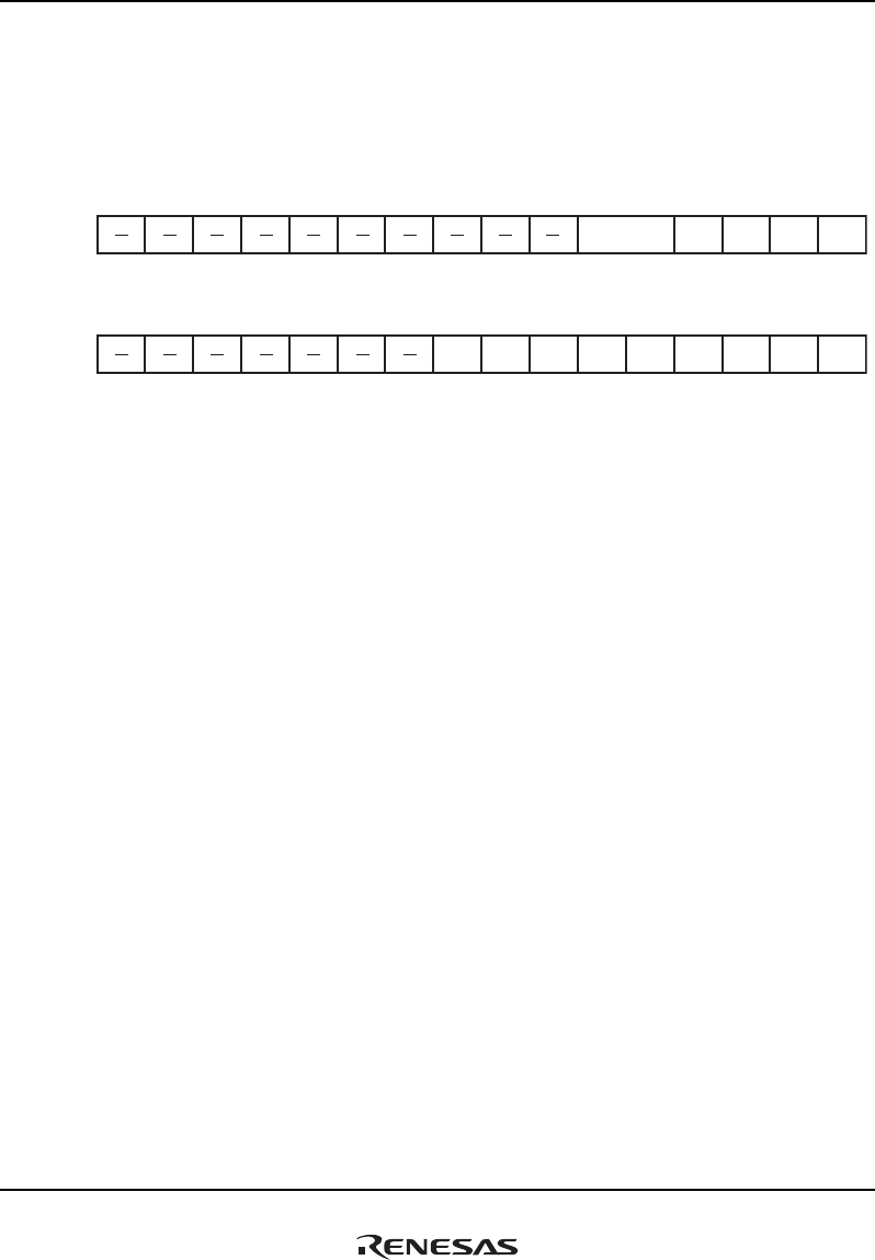
27. NAND Flash Memory Controller (FLCTL)
Rev.1.00 Jan. 10, 2008 Page 1354 of 1658
REJ09B0261-0100
27.3.8 Interrupt DMA Control Register (FLINTDMACR)
FLINTDMACR is a 32-bit readable/writable register that enables or disables DMA transfer
requests or interrupts. A transfer request from the FLCTL to the DMAC is issued after each access
mode has started.
31 30 29 28 27 26 25 24 23 22 21 20 19 18 17 16
15 14 13 12 11 10 9 8 7 6 5 4 3 2 1 0
0000000
0
000000000
R R R R R R R R R R R/W R/W R/W R/W R/W R/W
000000 000000000
R R R R R R R R/W R/W R/W R/W R/W R/W R/W R/W R/W
Bit:
Initial value:
R/W:
Bit:
Initial value:
R/W:
FIFOTRG[1:0] AC1
CLR
AC0
CLR
DREQ1
EN
DREQ0
EN
STE
RB
BTO
ERB
TRR
EQF1
TRR
EQF0
STER
INTE
RBER
INTE
TE
INTE
TR
INTE1
TR
INTE0

27. NAND Flash Memory Controller (FLCTL)
Rev.1.00 Jan. 10, 2008 Page 1355 of 1658
REJ09B0261-0100
Bit Bit Name
Initial
Value R/W Description
31 to 22 — All 0 R Reserved
These bits are always read as 0. The write value should
always be 0.
21, 20 FIFOTRG
[1:0]
00 R/W FIFO Trigger Setting
Change the condition for the FIFO transfer request.
(1) In reading flash memory
00: Issue an interrupt to the CPU or a DMA transfer
request when 4-byte data is written to
FLDTFIFO
01: Issue an interrupt to the CPU or a DMA transfer
request when 16-byte data is written to
FLDTFIFO
10: Issue an interrupt to the CPU or a DMA transfer
request when 128-byte data is written to
FLDTFIFO
11: Issue an interrupt to the CPU when FLDTFIFO
stores 128 bytes of data, or issue a DMA
transfer request when FLDTFIFO stores 16
bytes of data
(2) In writing flash memory
00: Issue an interrupt to the CPU when FLDTFIFO
has 4 bytes or more of empty area (do not set
DMA transfer)
01: Issue an interrupt or a DMA transfer request to
the CPU when FLDTFIFO has 16 bytes or more
of empty area
10: Issue an interrupt to the CPU when FLDTFIFO
has 128 bytes or more of empty area (do not
set DMA transfer)
11: Issue an interrupt to the CPU when FLDTFIFO
has 128 bytes or more of empty area, or issue a
DMA transfer request to the CPU when
FLDTFIFO has empty area of 16 bytes or more
19 AC1CLR 0 R/W FLECFIFO Clear
Clears the address counter of FLECFIFO.
0: Retains the address counter value of FLECFIFO. In
flash-memory access, clear this bit to 0.
1: Clears the address counter of FLECFIFO. After
clearing the counter, clear this bit to 0.

27. NAND Flash Memory Controller (FLCTL)
Rev.1.00 Jan. 10, 2008 Page 1356 of 1658
REJ09B0261-0100
Bit Bit Name
Initial
Value R/W Description
18 AC0CLR 0 R/W FLDTFIFO Clear
Clears the address counter of FLDTFIFO.
0: Retains the address counter value of FLDTFIFO. In
flash-memory access, clear this bit to 0.
1: Clears the address counter of FLDTFIFO. After
clearing the counter, clear this bit to 0
17 DREQ1EN 0 R/W FLECFIFODMA Request Enable
Enables or disables the DMA transfer request issued
from FLECFIFO.
0: Disables the issue of DMA transfer request from
FLECFIFO
1: Enables the issue of DMA transfer request from
FLECFIFO
16 DREQ0EN 0 R/W FLDTFIFODMA Request Enable
Enables or disables the DMA transfer request issued
from FLDTFIFO.
0: Disables the issue of DMA transfer request from
FLDTFIFO
1: Enables the issue of DMA transfer request from
FLDTFIFO
15 to 9 — All 0 R Reserved
These bits are always read as 0. The write value should
always be 0.
8 STERB 0 R/W Status Error
Indicates the result of status read. This bit is set to 1 if
the specific bit in bits STAT7 to STAT0 in FLBSYCNT is
set to 1 in status read.
Since this bit is a flag bit, 1 cannot be written to this bit.
Only 0 can be written to clear the flag.
0: Indicates that no status error occurs (the specific bit
in bits STAT7 to STAT0 in FLBSYCNT is 0.)
1: Indicates that a status error occurs
For details on the specific bit, see section 27.4.4, Status
Read.

27. NAND Flash Memory Controller (FLCTL)
Rev.1.00 Jan. 10, 2008 Page 1357 of 1658
REJ09B0261-0100
Bit Bit Name
Initial
Value R/W Description
7 BTOERB 0 R/W Timeout Error
This bit is set to 1 if a timeout error occurs (bits
RBTIMCNT20 to RBTIMCNT0 in FLBSYCNT are set to
0 after they are decremented).
Since this bit is a flag bit, 1 cannot be written to this bit.
Only 0 can be written to clear the flag.
0: Indicates that no timeout error occurs
1: Indicates that a timeout error occurs
6 TRREQF1 0 R/W FLECFIFO Transfer Request Flag
Indicates that a transfer request is issued from
FLECFIFO.
Since this bit is a flag bit, 1 cannot be written to this bit.
Only 0 can be written to clear the flag.
0: Indicates that no transfer request is issued from
FLECFIFO
1: Indicates that a transfer request is issued from
FLECFIFO
5 TRREQF0 0 R/W FLDTFIFO Transfer Request Flag
Indicates that a transfer request is issued from
FLDTFIFO.
Since this bit is a flag bit, 1 cannot be written to this bit.
Only 0 can be written to clear the flag.
0: Indicates that no transfer request is issued from
FLDTFIFO
1: Indicates that a transfer request is issued from
FLDTFIFO
4 STERINTE 0 R/W Interrupt Enable at Status Error
Enables or disables an interrupt request to the CPU
when a status error has occurred.
0: Disables the interrupt request to the CPU by a status
error
1: Enables the interrupt request to the CPU by a status
error

27. NAND Flash Memory Controller (FLCTL)
Rev.1.00 Jan. 10, 2008 Page 1358 of 1658
REJ09B0261-0100
Bit Bit Name
Initial
Value R/W Description
3 BTOINTE 0 RW Interrupt Enable at Timeout Error
Enables or disables an interrupt request to the CPU
when a timeout error has occurred.
0: Disables the interrupt request to the CPU by a
timeout error
1: Enables the interrupt request to the CPU by a
timeout error
2 TEINTE 0 R/W Transfer End Interrupt Enable
Enables or disables an interrupt request to the CPU
when a transfer has been ended (TREND bit in
FLTRCR).
0: Disables an interrupt to the CPU at the end of a
transfer
1: Enables an interrupt to the CPU at the end of a
transfer
1 TRINTE1 0 R/W FLECFIFO Transfer Request Enable to CPU
Enables or disables an interrupt request to the CPU by
a transfer request from FLECFIFO.
0: Disables an interrupt request to the CPU by a
transfer request from FLECFIFO.
1: Enables an interrupt request to the CPU by a transfer
request from FLECFIFO.
When the DMA transfer is enabled, this bit should be
cleared to 0.
0 TRINTE0 0 R/W FLDTFIFO Transfer Request Enable to CPU
Enables or disables an interrupt request to the CPU by
a transfer request from FLDTFIFO.
0: Disables an interrupt request to the CPU by a
transfer request from FLDTFIFO
1: Enables an interrupt request to the CPU by a transfer
request from FLDTFIFO
When the DMA transfer is enabled, this bit should be
cleared to 0.

27. NAND Flash Memory Controller (FLCTL)
Rev.1.00 Jan. 10, 2008 Page 1359 of 1658
REJ09B0261-0100
27.3.9 Ready Busy Timeout Setting Register (FLBSYTMR)
FLBSYTMR is a 32-bit readable/writable register that specifies the timeout time when the FRB
pin is busy.
31 30 29 28 27 26 25 24 23 22 21 20 19 18 17 16
15 14 13 12 11 10 9 8 7 6 5 4 3 2 1 0
0000000000000000
R R R R R R R R R R R R/W R/W R/W R/W R/W
0000000000000000
R/W R/W R/W R/W R/W R/W R/W R/W R/W R/W R/W R/W R/W R/W R/W R/W
Bit:
Initial value:
R/W:
Bit:
Initial value:
R/W:
RBTMOUT[20:16]
RBTMOUT[15:0]
Bit Bit Name
Initial
Value R/W Description
31 to 21 — All 0 R Reserved
These bits are always read as 0. The write value
should always be 0.
20 to 0 RBTMOUT[20:0] H'00000 R/W Ready Busy Timeout
Specify timeout time in the busy state
Set the timeout time in the busy state (with the clock
cycles of a peripheral clock)
When these bits are set to 0, timeout does not
occur.
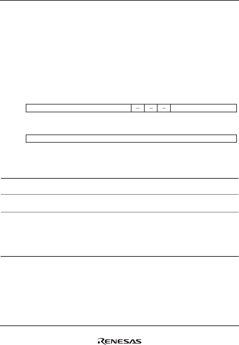
27. NAND Flash Memory Controller (FLCTL)
Rev.1.00 Jan. 10, 2008 Page 1360 of 1658
REJ09B0261-0100
27.3.10 Ready Busy Timeout Counter (FLBSYCNT)
FLBSYCNT is a 32-bit read-only register.
The status of flash memory read by the status read is stored in the bits STAT7 to STAT0.
The timeout time set in bits RBTMOUT20 to RBTMOUT0 in FLBSYTMR is copied to bits
RBTIMCNT20 to RBTIMCNT0 and counting down is started when the FRB pin enters the busy
state. When values in bits RBTIMCNT20 to RBTIMCNT0 are decremented to 0, 1 the BTOERB
bit in FLINTDMACR is set to 1, and the occurrence of a timeout error is notified. In this case, an
FLSTE interrupt can be issued if an interrupt is enabled by the RBERINTE bit in FLINTDMACR.
31 30 29 28 27 26 25 24 23 22 21 20 19 18 17 16
15 14 13 12 11 10 9 8 7 6 5 4 3 2 1 0
0000000000000000
RRRRRRRRRRRRRRRR
0000000000000000
RRRRRRRRRRRRRRRR
Bit:
Initial value:
R/W:
Bit:
Initial value:
R/W:
STAT[7:0] RBTIMCNT[20:16]
RBTIMCNT[15:0]
Bit Bit Name
Initial
Value R/W Description
31 to 24 STAT[7:0] H'00 R Indicate the value obtained by the status read from
flash memory
23 to 21 — All 0 R Reserved
These bits are always read as 0.
20 to 0 RBTIMCNT[20:0] H'00000 R Ready Busy Timeout Counter
When the FRB pin enters the busy state, the values
of bits RBTMOUT20 to RBTMOUT0 in FLBSYTMR
are copied to these bits. These bits are counted
down while the FRB pin is busy. A timeout error
occurs when these bits are decremented to 0.

27. NAND Flash Memory Controller (FLCTL)
Rev.1.00 Jan. 10, 2008 Page 1361 of 1658
REJ09B0261-0100
27.3.11 Data FIFO Register (FLDTFIFO)
FLDTFIFO is used to read from or write to the data FIFO area.
The read and write directions specified by the SELRW bit in FLCMDCR must match the read or
write access directions specified in this register.
31 30 29 28 27 26 25 24 23 22 21 20 19 18 17 16
15 14 13 12 11 10 9 8 7 6 5 4 3 2 1 0
R/W R/W R/W R/W R/W R/W R/W R/W R/W R/W R/W R/W R/W R/W R/W R/W
R/W R/W R/W R/W R/W R/W R/W R/W R/W R/W R/W R/W R/W R/W R/W R/W
Bit:
Initial value:
R/W:
Bit:
Initial value:
R/W:
DTFO[31:24] DTFO[23:16]
DTFO[15:8] DTFO[7:0]
————————————————
————————————————
Bit Bit Name
Initial
Value R/W Description
31 to 24 DTFO[31:24] ⎯ R/W First Data
Specify the first data to be input or output via the FD7 to
FD0 pins.
In writing: Specify write data
In reading: Store read data
23 to 16 DTFO[23:16] ⎯ R/W Second Data
Specify the second data to be input or output via the FD7
to FD0 pins.
In writing: Specify write data
In reading: Store read data
15 to 8 DTFO[15:8] ⎯ R/W Third Data
Specify the third data to be input or output via the FD7 to
FD0 pins.
In writing: Specify write data
In reading: Store read data
7 to 0 DTFO[7:0] ⎯ R/W Fourth Data
Specify the fourth data to be input or output via the FD7
to FD0 pins.
In writing: Specify write data
In reading: Store read data

27. NAND Flash Memory Controller (FLCTL)
Rev.1.00 Jan. 10, 2008 Page 1362 of 1658
REJ09B0261-0100
27.3.12 Control Code FIFO Register (FLECFIFO)
FLECFIFO is used to read from or write to the control code FIFO area.
The read and write directions specified by the SELRW bit in FLCMDCR must match the read and
write access directions specified in this register.
31 30 29 28 27 26 25 24 23 22 21 20 19 18 17 16
15 14 13 12 11 10 9 8 7 6 5 4 3 2 1 0
R/W R/W R/W R/W R/W R/W R/W R/W R/W R/W R/W R/W R/W R/W R/W R/W
R/W R/W R/W R/W R/W R/W R/W R/W R/W R/W R/W R/W R/W R/W R/W R/W
Bit:
Initial value:
R/W:
Bit:
Initial value:
R/W:
ECFO[31:24] ECFO[23:16]
ECFO[15:8] ECFO[7:0]
————————————————
————————————————
Bit Bit Name
Initial
Value R/W Description
31 to 24 ECFO[31:24] Undefined R/W First Data
Specify the first data to be input or output via the FD7 to
FD0 pins.
In writing: Specify write data
In reading: Store read data
23 to 16 ECFO[23:16] Undefined R/W Second Data
Specify the second data to be input or output via the
FD7 to FD0 pins.
In writing: Specify write data
In reading: Store read data
15 to 8 ECFO[15:8] Undefined R/W Third Data
Specify the third data to be input or output via the FD7
to FD0 pins.
In writing: Specify write data
In reading: Store read data
7 to 0 ECFO[7:0] Undefined R/W Fourth Data
Specify the fourth data to be input or output via the FD7
to FD0 pins.
In writing: Specify write data
In reading: Store read data

27. NAND Flash Memory Controller (FLCTL)
Rev.1.00 Jan. 10, 2008 Page 1363 of 1658
REJ09B0261-0100
27.3.13 Transfer Control Register (FLTRCR)
Setting the TRSTRT bit to 1 starts access to flash memory. The completion of the access can be
checked by the TREND bit.
76543210
00000000
RRRRRRR/W
R/W
Bit:
Initial value:
R/W:
TREND TRSTRT
Bit Bit Name
Initial
Value R/W Description
7 to 2 — All 0 R Reserved
These bits are always read as 0. The write value should
always be 0.
1 TREND 0 R/W Processing End Flag
Indicates that the processing performed in the specified
access mode has been completed. The write value
should always be 0.
0 TRSTRT 0 R/W Transfer Start
When the TREND bit is 0, processing in the access mode
specified by the access mode specification bits ACM[1:0]
is started by setting the TRSTRT bit from 0 to 1.
0: Stops transfer
1: Starts transfer
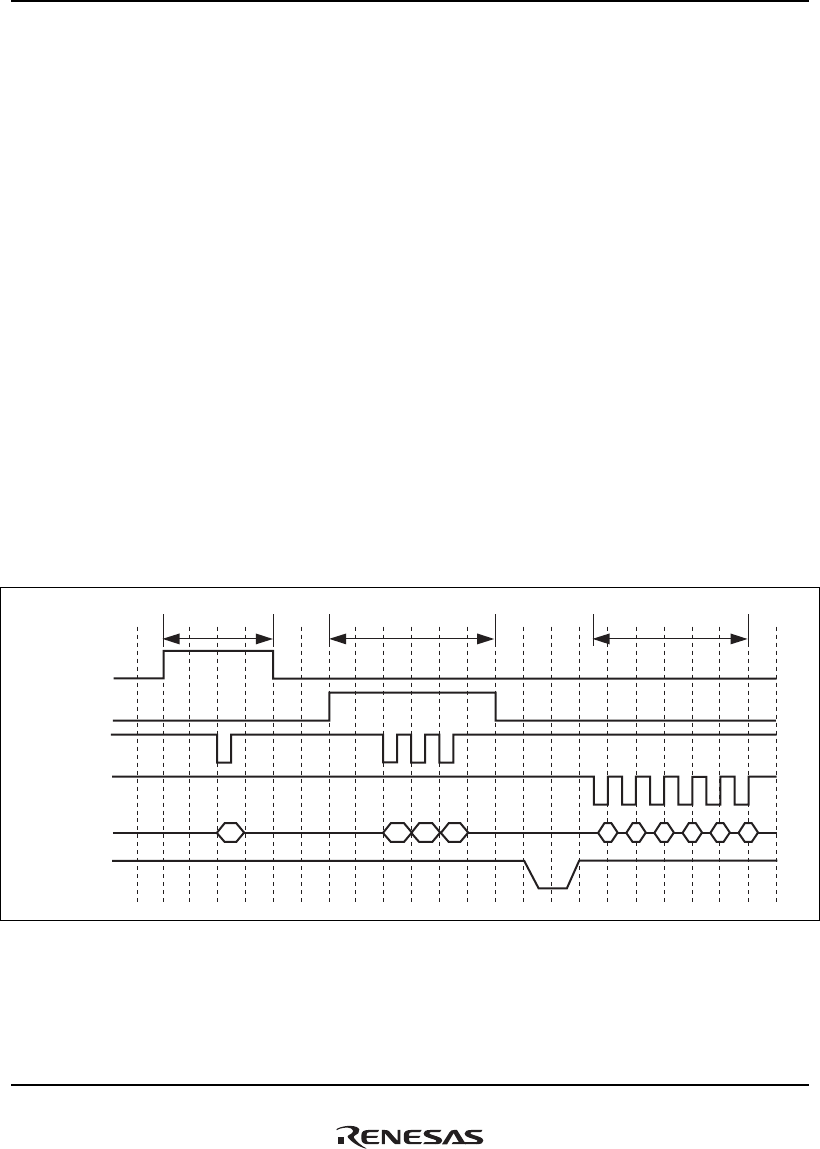
27. NAND Flash Memory Controller (FLCTL)
Rev.1.00 Jan. 10, 2008 Page 1364 of 1658
REJ09B0261-0100
27.4 Operation
27.4.1 Operating Modes
Two operating modes are supported.
• Command access mode
• Sector access mode
27.4.2 Command Access Mode
Command access mode is a mode that accesses flash memory by specifying a command to be
issued to flash memory, address, data, read or write direction, and number of times for the
registers. In this mode, DMA transfer of input or output data can be performed by using
FLDTFIFO.
(1) NAND-Type Flash Memory Access (512 + 16 Bytes)
Figure 27.2 shows an example of reading operation for NAND-type flash memory. In this
example, the first command is set to H'00, address data length is set to 3 bytes, and the number of
read bytes is set to 6 bytes in the data counter.
CLE
ALE
I/O7 to I/O0
R/B
H'00
A2A1 A3 1 2 3 4
WE
RE
56
Command stage Address stage Data stage
Figure 27.2 Reading Operation Timing for NAND-Type Flash Memory

27. NAND Flash Memory Controller (FLCTL)
Rev.1.00 Jan. 10, 2008 Page 1365 of 1658
REJ09B0261-0100
Figures 27.3 and 27.4 show examples of writing operation for NAND-type flash memory (512 +
16 bytes).
H'80
A2A1 A3 1 2 3 4 5 6
CLE
ALE
I/O7 to I/O0
R/B
WE
RE
Figure 27.3 Writing Operation Timing for NAND-Type Flash Memory
CLE
WE
RE
ALE
I/O7 to I/O0
R/B
H'10 H'70
Status
Figure 27.4 Status Read Operation Timing for NAND-Type Flash Memory
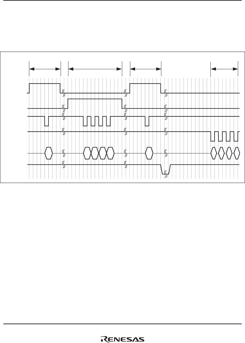
27. NAND Flash Memory Controller (FLCTL)
Rev.1.00 Jan. 10, 2008 Page 1366 of 1658
REJ09B0261-0100
(2) NAND-Type Flash Memory Access (2048 + 64 Bytes)
Figure 27.5 shows an example of reading operation for NAND-type flash memory. In this
example, the first command is set to H'00, the second command is set to H'30, address data length
is set to 4 bytes, and the number of read bytes is set to 4 bytes in the data counter.
CLE
ALE
I/O7 to I/O0
R/B
WE
RE
H'00
H'30
1
2
3
4
A1
A2
A3
A4
Command stage Address stage Data stageCommand stage
Figure 27.5 Reading Operation Timing for NAND-Type Flash Memory
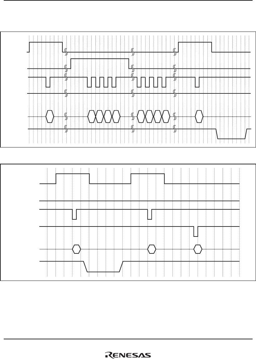
27. NAND Flash Memory Controller (FLCTL)
Rev.1.00 Jan. 10, 2008 Page 1367 of 1658
REJ09B0261-0100
Figures 27.6 and 27.7 show examples of writing operation for NAND-type flash memory (2048 +
64 bytes).
CLE
ALE
I/O7 to I/O0
R/B
WE
RE
H'80
A1
A2
A3
A4
1
2
3
4
H'10
Figure 27.6 Writing Operation Timing for NAND-Type Flash Memory
CLE
ALE
I/O7 to I/O0
R/B
WE
RE
H'10 H'70
Status
Figure 27.7 Status Read Operation Timing for NAND-Type Flash Memory
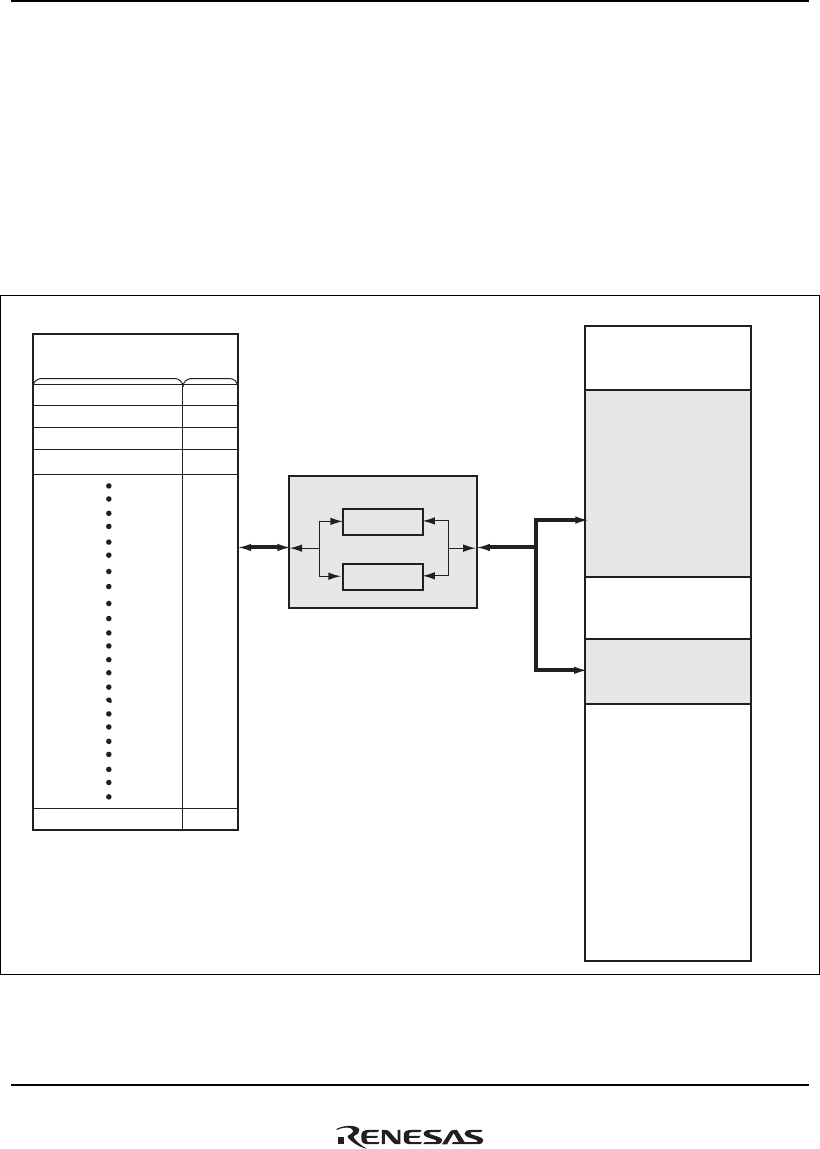
27. NAND Flash Memory Controller (FLCTL)
Rev.1.00 Jan. 10, 2008 Page 1368 of 1658
REJ09B0261-0100
27.4.3 Sector Access Mode
In sector access mode, flash memory can be read from or written to in sector units by specifying
the number of physical sectors to be accessed.
Since 512-byte data is stored in FLDTFIFO and 16-byte control code is stored in FLECFIFO,
DMA transfer can be performed by setting the DREQ1EN and DREQ0EN bits in FLINTDMACR.
Figure 27.8 shows the relationship of DMA transfer between sectors in flash memory (data and
control code) and memory in the address space.
FLCTL
FLDTFIFO
FLECFIFO
Flash memory
Data (512 bytes)
Control
code
(16 bytes)
DMA (channel 0)
transfer
DMA (channel 1)
transfer
Address space (external memory area)
Data area
Control code area
Figure 27.8 Diagram of DMA Transfer between Sector (Data and Control Code) in Flash
Memory and Memory in Address Space
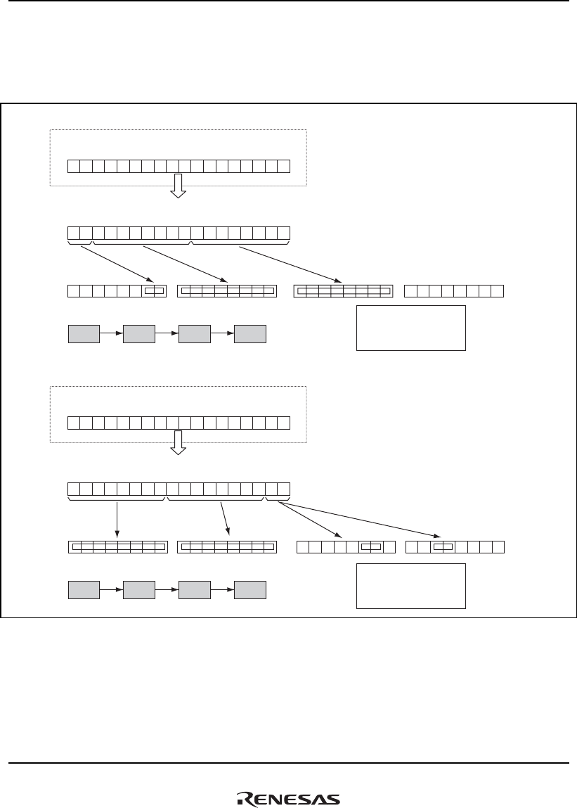
27. NAND Flash Memory Controller (FLCTL)
Rev.1.00 Jan. 10, 2008 Page 1369 of 1658
REJ09B0261-0100
(1) Physical Sector
Figure 27.9 shows the relationship between the physical sector address and flash memory address
of NAND-type flash memory.
Bit 17 Bit 0
Row3
Row3 Row2
Row2 Row1
Col: Column address
Row: Row address
(Page address)
Bit 17 Bit 0
Bit 17 Bit 0
000000
Col
00000000
Row1
Row2 Row1
Row2 Row1 Col
Bit 17 Bit 0
00 000 000000 0
Col1Col2
Col: Column address
Row: Row address
(Page address)
Col Row1 Row2 Row3
Col1 Col2 Row1 Row2
Physical sector address
• For NAND-type flash memory (512 + 16 bytes)
Physical sector address bits (FLADR[17:0])
Order of address output to NAND-type flash memory I/O
• For NAND-type flash memory (2048 + 64 bytes)
Physical sector address
Physical sector address bits (FLADR[17:0])
Order of address output to NAND-type flash memory I/O
Note: Since the address at each boundary
(512 + 16 bytes) of a column address is
generated by FLADR[1:0], when using
NAND-type flash memory (2048 + 64 bytes),
set
FLADR[1:0] as follows:
00: Address at byte 0
01: Address at (512 + 16)th byte
10: Address at (1024 + 32)th byte
11: Address at (1536 + 48)th byte
Figure 27.9 Example of Sector Number and NAND-Type Flash Memory Address
Expansion
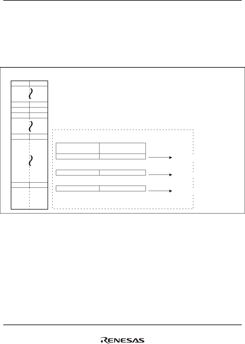
27. NAND Flash Memory Controller (FLCTL)
Rev.1.00 Jan. 10, 2008 Page 1370 of 1658
REJ09B0261-0100
(2) Continuous Sector Access
Continuous physical sectors can be read from or written to by specifying the start physical sector
address of NAND-type flash memory and the number of sectors to be transferred. Figure 27.10
shows an example of physical sector specification register and transfer count specification register
settings when transferring logical sectors 0 to 40, which are not contiguous because of an unusable
sector in NAND-type flash memory.
00 12
00
11 11
***12
13 13
40 40
300 12
300 1
13 28
(FLADR, ADR17 to ADR0) (FLCMDCR, SCTCNT)
Physical
sector
Values specified in registers by CPU
Physical sector
specification Physical sector
transfer count
Sectors 0 to 11 are transferred
Sector 12 is transferred
Sectors 13 to 40 are transferred
Logical
sector
Transfer start
Transfer start
Transfer start
Figure 27.10 Sector Access when Unusable Sector Is in Continuous Sectors

27. NAND Flash Memory Controller (FLCTL)
Rev.1.00 Jan. 10, 2008 Page 1371 of 1658
REJ09B0261-0100
27.4.4 Status Read
The FLCTL can read the status register of a NAND-type flash memory. The data in the status
register of a NAND-type flash memory is input through the I/O7 to I/O0 pins and stored in the bits
STAT7 to STAT0 in FLBSYCNT. The bits STAT7 to STAT0 in FLBSYCNT can be read by the
CPU. If a program error or erase error is detected when the status register value is stored in the
bits STAT7 to 0 in FLBSYCNT, the STERB bit in FLINTDMACR is set to 1 and generates an
interrupt to the CPU if the STERINTE bit in FLINTDMACR is enabled.
(1) Status Read of NAND-Type Flash Memory (512 + 16 Bytes)
The status read of NAND-type flash memory can be performed by inputting the command H'70 to
NAND-type flash memory. When the DOSR bit in FLCMDCR is set to 1 and writing is performed
in command access mode or sector access mode, the FLCTL automatically inputs H'70 to NAND-
type flash memory and status read is performed. During the status read of NAND-type flash
memory, the I/O7 to I/O0 pins indicate the following information as shown in table 27.4.
Table 27.4 Status Read of NAND-Type Flash Memory (512 + 16 Bytes)
I/O Status (Definition) Description
I/O7 Write protection 0: Cannot be written
1: Can be written
I/O6 Ready/busy 0: Busy state
1: Ready state
I/O5 to I/O1 Reserved ⎯
I/O0 Write/erase 0: Pass
1: Fail

27. NAND Flash Memory Controller (FLCTL)
Rev.1.00 Jan. 10, 2008 Page 1372 of 1658
REJ09B0261-0100
(2) Status Read of NAND-Type Flash Memory (2048 + 64 Bytes)
The status read of NAND-type flash memory can be performed by inputting the command H'70 to
NAND-type flash memory. When the DOSR bit in FLCMDCR is set to 1 and writing is performed
in command access mode or sector access mode, the FLCTL automatically inputs H'70 to NAND-
type flash memory and status read is performed. During the status read of NAND-type flash
memory, the I/O7 to I/O0 pins indicate the following information as shown in table 27.5.
Table 27.5 Status Read of NAND-Type Flash Memory (2048 + 64 Bytes)
I/O Status (Definition) Description
I/O7 Write protection 0: Cannot be written
1: Can be written
I/O6 Ready/busy 0: Busy state
1: Ready state
I/O5 Ready/busy 0: Busy state
1: Ready state
I/O4 to I/O1 Reserved 0
I/O0 Write/erase 0: Pass
1: Fail
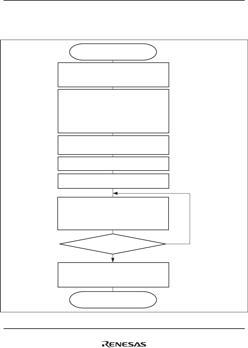
27. NAND Flash Memory Controller (FLCTL)
Rev.1.00 Jan. 10, 2008 Page 1373 of 1658
REJ09B0261-0100
27.5 Example of Register Setting
The examples of setting and starting registers in each access mode are shown below.
No
Yes
FLTRCR.TREND = B'1?
End of command access (block erase)
Start of command access (block erase)
Common control register (FLCMNCR)
ACM[1:0] = B'00 (command access mode)
CE0 = B'1 (enable the chip)
TYPESEL = B'1 (select NAND-type flash memory)
Command control register (FLCMDCR)
DOCMD1 = B'1 (execute first command stage)
DOCMD2 = B'1 (execute second command stage)
DOADR = B'1 (execute address stage)
ADRMD = B'1 (address register value is output as
memory address)
ADRCNT[1:0] = B'01 (issue 2-byte address)
DOSR = B'1 (perform status read)
Command code register (FLCMCDR)
CMD[7:0] = H'60 (block erase command)
CMD[15:8] = H'D0 (block erase execute command)
Address register (FLADR)
Set erase addresses to ADR[7:0] and ADR[15:8]
Transfer control register (FLTRCR)
TRSTRT = B'1 (start flash memory access)
Perform block erase of flash memory
Issue first command
Issue address
Issue second command
Read status
Set TRSTRT = B'1 (start flash memory access)
End of flash memory access
FLTRCR.TREND = B'0 (clear processing end flag)
Read status
Check FLBSYCNT.STAT[7:0]
Figure 27.11 NAND Command Access (Block Erase)

27. NAND Flash Memory Controller (FLCTL)
Rev.1.00 Jan. 10, 2008 Page 1374 of 1658
REJ09B0261-0100
Start of sector access (flash write)
FLTRCR.TREND = B'1?
End of sector access (flash write)
DMA source address registers (SAR0 and SAR1)
SAR0[31:0]: Set start address of data to be written
SAR1[31:0]: Set start address of control code to be written
DMA destination address registers (DAR0 and DAR1)
DAR0[31:0]: Set FLDTFIFO address
DAR1[31:0]: Set FLECFIFO address
DMA transfer count registers (TCR0 and TCR1)
TCR0[31:0] = H'0000 0080 (512 bytes = 4 × 128)
TCR1[31:0] = H'0000 0004 (16 bytes = 4 × 4)
DMA channel control registers (CHCR0 and CHCR1)
SM[1:0] = B'01 (DMA transfer source address is
incremented)
RS[3:0] = B'1000 (DMA extended resource selector)
TS[2:0] = B'010 (longword transfer)
DE = B'1 (enable DMA transfer)
DMA extended resource selector (DMARS0)
DMARS0[15:0] = H'8783 (FLCTL data and control code
part transmission/reception)
DMA operation register (DMAOR)
DME = B'1 (enable DMA transfer for all channels)
Common control register (FLCMNCR)
ACM[1:0] = B'01 (sector access mode)
CE0 = B'1 (enable the chip)
TYPESEL = B'1 (select NAND-type flash memory)
Command control register (FLCMDCR)
SELRW = B'1 (flash write)
DOCMD1 = B'1 (execute first command stage)
DOCMD2 = B'1 (execute second command stage)
DOADR = B'1 (execute address stage)
ADRMD = B'1 (specify physical sector address)
ADRCNT[1:0] = B'10 (issue 3-byte address)
DOSR = B'1 (perform status read)
Specify number of sector transfers to SCTCNT[15:0]
(1 sector)
Command code register (FLCMCDR)
CMD[7:0] = H'80 (flash write command)
CMD[15:8] = H'10 (flash write execute command)
Address register (FLADR)
Specify physical sector address to ADR[17:0]
End of flash memory access
FLTRCR.TREND = 0 (clear processing end flag)
Read status
Check FLBSYCNT.STAT[7:0]
Perform flash memory writing
Issue first command
Issue address
Data stage (sector access)
Issue second command
Read status
Transfer control register (FLTRCR)
TRSTRT = B'1 (start flash memory access)
Interrupt DMA control register (FLINTDMACR)
DREQ1EN = B'1
(enable DMA transfer request from FLECFIFO)
DREQ0EN = B'1
(enable DMA transfer request from FLDTFIFO)
No
Yes
Figure 27.12 NAND Sector Access (Flash Write) Using DMAC

27. NAND Flash Memory Controller (FLCTL)
Rev.1.00 Jan. 10, 2008 Page 1375 of 1658
REJ09B0261-0100
Start of command access (flash read)
FLTRCR.TREND = B'1?
End of command access (flash read)
Yes
No
Common control register (FLCMNCR)
ACM[1:0] = B'00 (command access mode)
CE0 = B'1 (enable the chip)
TYPESEL = B'1 (select NAND-type flash memory)
Command control register (FLCMDCR)
DOCMD1 = B'1 (execute first command stage)
DOADR = B'1 (execute address stage)
ADRMD = B'1 (address register value is output as
memory address)
ADRCNT[1:0] = B'10 (issue 3-byte address)
DOSR = B'1 (perform status read)
Command code register (FLCMCDR)
CMD[7:0] = H'00 (flash read command)
Address register (FLADR)
Set addresses to ADR[7:0], ADR[15:8], and ADR[23:16]
Data counter register (FLDTCNTR)
Specify number of bytes of read data to DTCNT[11:0]
Interrupt DMA control register (FLINTDMACR)
Set enable bit of DMA transfer or interrupt request to 1
Transfer control register (FLTRCR)
TRSTRT = B'1 (start flash memory access)
Perform flash memory reading
Issue first command
Issue address
Issue second command
Read status
End of flash memory access
FLTRCR.TREND = B'0 (clear processing end flag)
Read status
Check FLBSYCNT.STAT[7:0]
Figure 27.13 NAND Command Access (Flash Read)

27. NAND Flash Memory Controller (FLCTL)
Rev.1.00 Jan. 10, 2008 Page 1376 of 1658
REJ09B0261-0100
27.6 Interrupt Processing
The FLCTL has four interrupt sources. Each of the interrupt sources has its corresponding
interrupt flag. The interrupt request is generated independently if the interrupt is enabled by the
interrupt enable bit. The status error and ready/busy timeout error use the common FLSTE
interrupt.
Table 27.6 FLCTL Interrupt Requests
Interrupt Source Interrupt Flag Enable Bit Description
STERB STERINTE Status error FLSTE interrupt
BTOERB RBERINTE Ready/busy timeout error
FLTEND interrupt TREND TEINTE Transfer end
FLTRQ0 interrupt TRREQF0 TRINTE0 FIFO0 transfer request
FLTRQ1 interrupt TRREQF1 TRINTE1 FIFO1 transfer request
27.7 DMA Transfer Settings
The FLCTL can request DMA transfers separately to the data sector, FLDTFIFO, and control
code sector, FLECFIFO. Table 27.7 shows whether DMA transfer is enabled or disabled in each
access mode.
Table 27.7 DMA Transfer Settings
Sector Access Mode Command Access Mode
FLDTFIFO Enabled Enabled
FLECFIFO Enabled Disabled
For details on DMAC settings, see section 14, Direct Memory Access Controller (DMAC).

28. General Purpose I/O Ports (GPIO)
Rev.1.00 Jan. 10, 2008 Page 1377 of 1658
REJ09B0261-0100
Section 28 General Purpose I/O Ports (GPIO)
28.1 Features
This LSI has sixteen general-purpose ports (A to H, J to N, and P to R), which provide 111
input/output pins.
The general-purpose I/O (GPIO) port pins are multiplexed with the pins of peripheral modules to
select whether the pins are used by the GPIO or the peripheral modules.
The GPIO has the following features.
• Each port pin is a multiplexed pin, for which the port control register can specify the pin
function and control the pull-up MOS of the pin.
• Each port has a data register that stores data for the pins.
• GPIO interrupts are supported*.
Note: * For the ports which can be used as GPIO interrupt pins, refer to table 28.1. For GPIO
interrupt settings, refer to section 10, Interrupt Controller (INTC).

28. General Purpose I/O Ports (GPIO)
Rev.1.00 Jan. 10, 2008 Page 1378 of 1658
REJ09B0261-0100
Table 28.1 Multiplexed Pins Controlled by Port Control Registers
Pin Name Port GPIO Selectable Module
GPIO
Interrupt
D63/AD31*2 A PA7 input/output LBSC/PCIC ⎯
D62/AD30*2 A PA6 input/output LBSC/PCIC ⎯
D61/AD29*2 A PA5 input/output LBSC/PCIC ⎯
D60/AD28*2 A PA4 input/output LBSC/PCIC ⎯
D59/AD27*2 A PA3 input/output LBSC/PCIC ⎯
D58/AD26*2 A PA2 input/output LBSC/PCIC ⎯
D57/AD25*2 A PA1 input/output LBSC/PCIC ⎯
D56/AD24*2 A PA0 input/output LBSC/PCIC ⎯
D55/AD23*2 B PB7 input/output LBSC/PCIC ⎯
D54/AD22*2 B PB6 input/output LBSC/PCIC ⎯
D53/AD21*2 B PB5 input/output LBSC/PCIC ⎯
D52/AD20*2 B PB4 input/output LBSC/PCIC ⎯
D51/AD19*2 B PB3 input/output LBSC/PCIC ⎯
D50/AD18*2 B PB2 input/output LBSC/PCIC ⎯
D49/AD17/DB5*2 B PB1 input/output LBSC/PCIC/DU ⎯
D48/AD16/DB4*2 B PB0 input/output LBSC/PCIC/DU ⎯
D47/AD15/DB3*2 C PC7 input/output LBSC/PCIC/DU ⎯
D46/AD14/DB2*2 C PC6 input/output LBSC/PCIC/DU ⎯
D45/AD13/DB1*2 C PC5 input/output LBSC/PCIC/DU ⎯
D44/AD12/DB0*2 C PC4 input/output LBSC/PCIC/DU ⎯
D43/AD11/DG5*2 C PC3 input/output LBSC/PCIC/DU ⎯
D42/AD10/DG4*2 C PC2 input/output LBSC/PCIC/DU ⎯
D41/AD9/DG3*2 C PC1 input/output LBSC/PCIC/DU ⎯
D40/AD8/DG2*2 C PC0 input/output LBSC/PCIC/DU ⎯
D39/AD7/DG1*2 D PD7 input/output LBSC/PCIC/DU ⎯
D38/AD6/DG0*2 D PD6 input/output LBSC/PCIC/DU ⎯
D37/AD5/DR5*2 D PD5 input/output LBSC/PCIC/DU ⎯
D36/AD4/DR4*2 D PD4 input/output LBSC/PCIC/DU ⎯
D35/AD3/DR3*2 D PD3 input/output LBSC/PCIC/DU ⎯
D34/AD2/DR2*2 D PD2 input/output LBSC/PCIC/DU ⎯

28. General Purpose I/O Ports (GPIO)
Rev.1.00 Jan. 10, 2008 Page 1379 of 1658
REJ09B0261-0100
Pin Name Port GPIO Selectable Module
GPIO
Interrupt
D33/AD1/DR1*2 D PD1 input/output LBSC/PCIC/DU ⎯
D32/AD0/DR0*2 D PD0 input/output LBSC/PCIC/DU ⎯
REQ1 E PE5 input/output PCIC Available
REQ2 E PE4 input/output PCIC Available
REQ3*1 E PE3 input/output PCIC Available
GNT1 E PE2 input/output PCIC Available
GNT2 E PE1 input/output PCIC Available
GNT3/MMCCLK*1 E PE0 input/output PCIC/MMCIF Available
D31 F PF7 input/output LBSC ⎯
D30 F PF6 input/output LBSC ⎯
D29 F PF5 input/output LBSC ⎯
D28 F PF4 input/output LBSC ⎯
D27 F PF3 input/output LBSC ⎯
D26 F PF2 input/output LBSC ⎯
D25 F PF1 input/output LBSC ⎯
D24 F PF0 input/output LBSC ⎯
D23 G PG7 input/output LBSC ⎯
D22 G PG6 input/output LBSC ⎯
D21 G PG5 input/output LBSC ⎯
D20 G PG4 input/output LBSC ⎯
D19 G PG3 input/output LBSC ⎯
D18 G PG2 input/output LBSC ⎯
D17 G PG1 input/output LBSC ⎯
D16 G PG0 input/output LBSC ⎯
SCIF1_SCK H PH7 input/output SCIF1 ⎯
SCIF1_RXD H PH6 input/output SCIF1 ⎯
SCIF1_TXD H PH5 input/output SCIF1 ⎯
SCIF0_CTS/INTD/FCE*1 H PH4 input/output SCIF0/PCIC/FLCTL Available
SCIF0_RTS/HSPI_CS/FSE*1 H PH3 input/output SCIF0/HSPI/FLCTL Available
SCIF0_SCK/HSPI_CLK/FRE*1 H PH2 input/output SCIF0/HSPI/FLCTL Available
SCIF0_RXD/HSPI_RX/FRB*1 H PH1 input/output SCIF0/HSPI/FLCTL Available

28. General Purpose I/O Ports (GPIO)
Rev.1.00 Jan. 10, 2008 Page 1380 of 1658
REJ09B0261-0100
Pin Name Port GPIO Selectable Module
GPIO
Interrupt
SCIF0_TXD/HSPI_TX/FWE*1 H PH0 input/output SCIF0/HSPI/FLCTL ⎯
SCIF5_TXD/HAC1_SYNC/SSI1_WS*1 J PJ7 input/output SCIF5/HAC1/SSI1 ⎯
SIOF_TXD/HAC0_SDOUT/
SSI0_SDATA*1
J PJ6 input/output SCOF/HAC0/SSI0 ⎯
SIOF_RXD/HAC0_SDIN/SSI0_SCK*1 J PJ5 input/output SIOF/HAC0/SSI0 ⎯
SIOF_SYNC/HAC0_SYNC/SSI0_WS*1 J PJ4 input/output SIOF/HAC0/SSI0 ⎯
SIOF_MCLK/HAC_RES*1 J PJ3 input/output SIOF/HAC ⎯
SIOF_SCK/HAC0_BITCLK/SSI0_CLK*1 J PJ2 input/output SIOF/HAC0/SSI0 ⎯
HAC1_BITCLK/SSI1_CLK*1 J PJ1 input/output HAC1/SSI1 ⎯
MODE13/TCLK/IOIS16*1 J PJ0 input/output —/TMU/LBSC ⎯
STATUS0/DRAK0*1 K PK7 input/output [STATUS]/DMAC ⎯
STATUS1/DRAK1*1 K PK6 input/output [STATUS]/DMAC ⎯
DACK2/SCIF2_TXD/MMCCMD/
SIOF_TXD*1
K PK5 input/output DMAC/SCIF2/MMCIF/
SIOF
⎯
DACK3/SCIF2_SCK/MMCDAT/
SIOF_SCK*1
K PK4 input/output DMAC/SCIF2/MMCIF/
SIOF
⎯
DREQ0 K PK3 input/output DMAC ⎯
DREQ1 K PK2 input/output DMAC ⎯
DACK0 K PK1 input/output DMAC ⎯
DACK1 K PK0 input/output DMAC ⎯
DREQ2/INTB*1 L PL7 input/output DMAC/PCIC Available
DREQ3/INTC*1 L PL6 input/output DMAC/PCIC Available
DRAK2/CE2A*1 L PL5 input/output DMAC/LBSC ⎯
MODE0/IRL4/FD4*1 L PL4 input/output ⎯/INTC/FLCTL ⎯
MODE1/IRL5/FD5*1 L PL3 input/output ⎯/INTC/FLCTL ⎯
MODE2/IRL6/FD6*1 L PL2 input/output ⎯/INTC/FLCTL ⎯
MODE3/IRL7/FD7*1 L PL1 input/output ⎯/INTC/FLCTL ⎯
MODE12/DRAK3/CE2B*1 L PL0 input/output ⎯/DMAC/LBSC ⎯
BREQ/BSACK M PM1 input/output LBSC ⎯
BACK/BSREQ M PM0 input/output LBSC ⎯
SCIF5_RXD/HAC1_SDIN/SSI1_SCK*1 N PN7 input/output SCIF5/HAC1/SS1 ⎯

28. General Purpose I/O Ports (GPIO)
Rev.1.00 Jan. 10, 2008 Page 1381 of 1658
REJ09B0261-0100
Pin Name Port GPIO Selectable Module
GPIO
Interrupt
SCIF5_SCK/HAC1_SDOUT/
SSI1_SDATA*1
N PN6 input/output SCIF5/HAC1/SS1 ⎯
MODE4/SCIF3_TXD/FCLE*1 N PN5 input/output ⎯/SCIF3/FLCTL ⎯
MODE7/SCIF3_RXD/FALE*1 N PN4 input/output ⎯/SCIF3/FLCTL ⎯
MODE8/SCIF3_SCK/FD0*1 N PN3 input/output ⎯/SCIF3/FLCTL ⎯
MODE9/SCIF4_TXD/FD1*1 N PN2 input/output ⎯/SCIF4/FLCTL ⎯
MODE10/SCIF4_RXD/FD2*1 N PN1 input/output ⎯/SCIF4/FLCTL ⎯
MODE11/SCIF4_SCK/FD3*1 N PN0 input/output ⎯/SCIF4/FLCTL ⎯
DEVSEL/DCLKOUT*2 P PP5 input/output PCIC/DU ⎯
STOP/CDE*2 P PP4 input/output PCIC/DU ⎯
LOCK/ODDF*2 P PP3 input/output PCIC/DU ⎯
TRDY/DISP*2 P PP2 input/output PCIC/DU ⎯
IRDY/HSYNC*2 P PP1 input/output PCIC/DU ⎯
PCIFRAME/VSYNC*2 P PP0 input/output PCIC/DU ⎯
INTA Q PQ4 input/output PCIC ⎯
GNT0/GNTIN Q PQ3 input/output PCIC ⎯
REQ0/REQOUT Q PQ2 input/output PCIC ⎯
PERR Q PQ1 input/output PCIC ⎯
SERR Q PQ0 input/output PCIC ⎯
WE7/CBE3*2 R PR3 input/output LBSC/PCIC ⎯
WE6/CBE2*2 R PR2 input/output LBSC/PCIC ⎯
WE5/CBE1*2 R PR1 input/output LBSC/PCIC ⎯
WE4/CBE0*2 R PR0 input/output LBSC/PCIC ⎯
PCICLK/DCLKIN*2 ⎯ ⎯ PCIC/DU ⎯
SCIF2_RXD/SIOF_RXD*1 ⎯ ⎯ SCIF2/SIOF ⎯
MODE5/SIOF_MCLK*1 ⎯ ⎯ ⎯/SIOF ⎯
MODE6/SIOF_SYNC*1 ⎯ ⎯ ⎯/SIOF ⎯
MRESETOUT/IRQOUT*1 ⎯ ⎯ RESET/INTC ⎯
Notes: 1. The module that uses this pin is selected by the peripheral module select registers 1
and 2 (P1MSELR and P2MSELR).
2. The module that uses this pin is selected by the bus mode pins (MODE11 and
MODE12). For the details of bus mode pin setting, refer to the Appendix.

28. General Purpose I/O Ports (GPIO)
Rev.1.00 Jan. 10, 2008 Page 1382 of 1658
REJ09B0261-0100
28.2 Register Descriptions
The following registers are provided to control the GPIO ports.
Table 28.2 Register Configuration (1)
Register Name Abbrev. R/W P4 Address*1
Area 7
Address*1
Access
Size*2
Sync
Clock
Port A control register PACR R/W H'FFE7 0000 H'1FE7 0000 16 Pck
Port B control register PBCR R/W H'FFE7 0002 H'1FE7 0002 16 Pck
Port C control register PCCR R/W H'FFE7 0004 H'1FE7 0004 16 Pck
Port D control register PDCR R/W H'FFE7 0006 H'1FE7 0006 16 Pck
Port E control register PECR R/W H'FFE7 0008 H'1FE7 0008 16 Pck
Port F control register PFCR R/W H'FFE7 000A H'1FE7 000A 16 Pck
Port G control register PGCR R/W H'FFE7 000C H'1FE7 000C 16 Pck
Port H control register PHCR R/W H'FFE7 000E H'1FE7 000E 16 Pck
Port J control register PJCR R/W H'FFE7 0010 H'1FE7 0010 16 Pck
Port K control register PKCR R/W H'FFE7 0012 H'1FE7 0012 16 Pck
Port L control register PLCR R/W H'FFE7 0014 H'1FE7 0014 16 Pck
Port M control register PMCR R/W H'FFE7 0016 H'1FE7 0016 16 Pck
Port N control register PNCR R/W H'FFE7 0018 H'1FE7 0018 16 Pck
Port P control register PPCR R/W H'FFE7 001A H'1FE7 001A 16 Pck
Port Q control register PQCR R/W H'FFE7 001C H'1FE7 001C 16 Pck
Port R control register PRCR R/W H'FFE7 001E H'1FE7 001E 16 Pck
Port A data register PADR R/W H'FFE7 0020 H'1FE7 0020 8 Pck
Port B data register PBDR R/W H'FFE7 0022 H'1FE7 0022 8 Pck
Port C data register PCDR R/W H'FFE7 0024 H'1FE7 0024 8 Pck
Port D data register PDDR R/W H'FFE7 0026 H'1FE7 0026 8 Pck
Port E data register PEDR R/W H'FFE7 0028 H'1FE7 0028 8 Pck
Port F data register PFDR R/W H'FFE7 002A H'1FE7 002A 8 Pck
Port G data register PGDR R/W H'FFE7 002C H'1FE7 002C 8 Pck
Port H data register PHDR R/W H'FFE7 002E H'1FE7 002E 8 Pck
Port J data register PJDR R/W H'FFE7 0030 H'1FE7 0030 8 Pck

28. General Purpose I/O Ports (GPIO)
Rev.1.00 Jan. 10, 2008 Page 1383 of 1658
REJ09B0261-0100
Register Name Abbrev. R/W P4 Address*1
Area 7
Address*1
Access
Size*2
Sync
Clock
Port K data register PKDR R/W H'FFE7 0032 H'1FE7 0032 8 Pck
Port L data register PLDR R/W H'FFE7 0034 H'1FEA 0034 8 Pck
Port M data register PMDR R/W H'FFE7 0036 H'1FEA 0036 8 Pck
Port N data register PNDR R/W H'FFE7 0038 H'1FEA 0038 8 Pck
Port P data register PPDR R/W H'FFE7 003A H'1FEA 003A 8 Pck
Port Q data register PQDR R/W H'FFE7 003C H'1FEA 003C 8 Pck
Port R data register PRDR R/W H'FFE7 003E H'1FEA 003E 8 Pck
Port E pull-up control register PEPUPR R/W H'FFE7 0048 H'1FEA 0048 8 Pck
Port H pull-up control register PHPUPR R/W H'FFE7 004E H'1FEA 004E 8 Pck
Port J pull-up control register PJPUPR R/W H'FFE7 0050 H'1FE7 0050 8 Pck
Port K pull-up control register PKPUPR R/W H'FFE7 0052 H'1FE7 0052 8 Pck
Port L pull-up control register PLPUPR R/W H'FFE7 0054 H'1FE7 0054 8 Pck
Port M pull-up control register PMPUPR R/W H'FFE7 0056 H'1FE7 0056 8 Pck
Port N pull-up control register PNPUPR R/W H'FFE7 0058 H'1FE7 0058 8 Pck
Input pin pull-up control register 1 PPUPR1 R/W H'FFE7 0060 H'1FE7 0060 16 Pck
Input pin pull-up control register 2 PPUPR2 R/W H'FFE7 0062 H'1FE7 0062 16 Pck
Peripheral module select register
1
P1MSELR R/W H'FFE7 0080 H'1FE7 0080 16 Pck
Peripheral module select register
2
P2MSELR R/W H'FFE7 0082 H'1FE7 0082 16 Pck
Notes: 1. The P4 area address uses the P4 area of the logical address area. The area 7 address
is accessed from area 7 of the physical address space using the TLB.
2. There are 8-bit and 16-bit registers. The registers must be accessed in the designate
size.

28. General Purpose I/O Ports (GPIO)
Rev.1.00 Jan. 10, 2008 Page 1384 of 1658
REJ09B0261-0100
Table 28.2 Register Configuration (2)
Register Name Abbrev.
Power-on
Reset by
RESET
Pin/WDT/
H-UDI
Manual
Reset by
WDT/
Multiple
Exception
Sleep
by SLEEP
Instruction
Module
Standby
Deep
Sleep
Port A control register PACR H'0000 Retained Retained Retained Retained
Port B control register PBCR H'0000 Retained Retained Retained Retained
Port C control register PCCR H'0000 Retained Retained Retained Retained
Port D control register PDCR H'0000 Retained Retained Retained Retained
Port E control register PECR H'00C3 Retained Retained Retained Retained
Port F control register PFCR H'0000 Retained Retained Retained Retained
Port G control register PGCR H'0000 Retained Retained Retained Retained
Port H control register PHCR H'FFFF Retained Retained Retained Retained
Port J control register PJCR H'FFFF Retained Retained Retained Retained
Port K control register PKCR H'0FFF Retained Retained Retained Retained
Port L control register PLCR H'FFFF Retained Retained Retained Retained
Port M control register PMCR H'FFF0 Retained Retained Retained Retained
Port N control register PNCR H'FFFF Retained Retained Retained Retained
Port P control register PPCR H'0000 Retained Retained Retained Retained
Port Q control register PQCR H'0000 Retained Retained Retained Retained
Port R control register PRCR H'0000 Retained Retained Retained Retained
Port A data register PADR H'00 Retained Retained Retained Retained
Port B data register PBDR H'00 Retained Retained Retained Retained
Port C data register PCDR H'00 Retained Retained Retained Retained
Port D data register PDDR H'00 Retained Retained Retained Retained
Port E data register PEDR H'0x Retained Retained Retained Retained
Port F data register PFDR H'00 Retained Retained Retained Retained
Port G data register PGDR H'00 Retained Retained Retained Retained
Port H data register PHDR H'00 Retained Retained Retained Retained
Port J data register PJDR H'xx Retained Retained Retained Retained
Port K data register PKDR H'xx Retained Retained Retained Retained
Port L data register PLDR H'xx Retained Retained Retained Retained
Port M data register PMDR H'xx Retained Retained Retained Retained
Port N data register PNDR H'xx Retained Retained Retained Retained
Port P data register PPDR H'00 Retained Retained Retained Retained
Port Q data register PQDR H'00 Retained Retained Retained Retained

28. General Purpose I/O Ports (GPIO)
Rev.1.00 Jan. 10, 2008 Page 1385 of 1658
REJ09B0261-0100
Register Name Abbrev.
Power-on
Reset by
RESET
Pin/WDT/
H-UDI
Manual
Reset by
WDT/
Multiple
Exception
Sleep
by SLEEP
Instruction
Module
Standby
Deep
Sleep
Port R data register PRDR H'00 Retained Retained Retained Retained
Port E pull-up control register PEPUPR H'FF Retained Retained Retained Retained
Port H pull-up control register PHPUPR H'FF Retained Retained Retained Retained
Port J pull-up control register PJPUPR H'FF Retained Retained Retained Retained
Port K pull-up control register PKPUPR H'FF Retained Retained Retained Retained
Port L pull-up control register PLPUPR H'FF Retained Retained Retained Retained
Port M pull-up control register PMPUPR H'FF Retained Retained Retained Retained
Port N pull-up control register PNPUPR H'FF Retained Retained Retained Retained
Input pin pull-up control register 1 PPUPR1 H'FFFF Retained Retained Retained Retained
Input pin pull-up control register 2 PPUPR2 H'FFFF Retained Retained Retained Retained
Peripheral module select register 1 P1MSELR H'0000 Retained Retained Retained Retained
Peripheral module select register 2 P2MSELR H'0000 Retained Retained Retained Retained

28. General Purpose I/O Ports (GPIO)
Rev.1.00 Jan. 10, 2008 Page 1386 of 1658
REJ09B0261-0100
28.2.1 Port A Control Register (PACR)
PACR is a 16-bit readable/writable register that selects the pin function and controls the input
pull-up MOS.
01234567891011121315 14
0000000000000000
PA0
MD0
PA0
MD1
PA1
MD0
PA1
MD1
PA2
MD0
PA2
MD1
PA3
MD0
PA3
MD1
PA4
MD0
PA4
MD1
PA5
MD0
PA5
MD1
PA6
MD0
PA6
MD1
PA7
MD1 PA7
MD0
R/WR/WR/WR/WR/WR/WR/WR/WR/WR/WR/WR/WR/WR/WR/W R/W
Bit:
Initial value:
R/W:
Bit Bit Name
Initial
value R/W Description
15
14
PA7MD1
PA7MD0
0
0
R/W
R/W
PA7 Mode
00: LBSC/PCIC module (D63/AD31)*
When the bus mode is set to DU via the bus-mode
pins (MODE11 and MODE12), port input (pull-up
MOS: On) is selected.
01: Port output
10: Port input (pull-up MOS: Off)
11: Port input (pull-up MOS: On)
13
12
PA6MD1
PA6MD0
0
0
R/W
R/W
PA6 Mode
00: LBSC/PCIC module (D62/AD30)*
When the bus mode is set to DU via the bus-mode
pins (MODE11 and MODE12), port input (pull-up
MOS: On) is selected.
01: Port output
10: Port input (pull-up MOS: Off)
11: Port input (pull-up MOS: On)
11
10
PA5MD1
PA5MD0
0
0
R/W
R/W
PA5 Mode
00: LBSC/PCIC module (D61/AD29)*
When the bus mode is set to DU via the bus-mode
pins (MODE11 and MODE12), port input (pull-up
MOS: On) is selected.
01: Port output
10: Port input (pull-up MOS: Off)
11: Port input (pull-up MOS: On)

28. General Purpose I/O Ports (GPIO)
Rev.1.00 Jan. 10, 2008 Page 1387 of 1658
REJ09B0261-0100
Bit Bit Name
Initial
value R/W Description
9
8
PA4MD1
PA4MD0
0
0
R/W
R/W
PA4 Mode
00: LBSC/PCIC module (D60/AD28)*
When the bus mode is set to DU via the bus-mode
pins (MODE11 and MODE12), port input (pull-up
MOS: On) is selected.
01: Port output
10: Port input (pull-up MOS: Off)
11: Port input (pull-up MOS: On)
7
6
PA3MD1
PA3MD0
0
0
R/W
R/W
PA3 Mode
00: LBSC/PCIC module (D59/AD27)*
When the bus mode is set to DU via the bus-mode
pins (MODE11 and MODE12), port input (pull-up
MOS: On) is selected.
01: Port output
10: Port input (pull-up MOS: Off)
11: Port input (pull-up MOS: On)
5
4
PA2MD1
PA2MD0
0
0
R/W
R/W
PA2 Mode
00: LBSC/PCIC module (D58/AD26)*
When the bus mode is set to DU module via the
bus-mode pins (MODE11 and MODE12), port input
(pull-up MOS: On) is selected.
01: Port output
10: Port input (pull-up MOS: Off)
11: Port input (pull-up MOS: On)
3
2
PA1MD1
PA1MD0
0
0
R/W
R/W
PA1 Mode
00: LBSC/PCIC module (D57/AD25)*
When the bus mode is set to DU via the bus-mode
pins (MODE11 and MODE12), port input (pull-up
MOS: On) is selected.
01: Port output
10: Port input (pull-up MOS: Off)
11: Port input (pull-up MOS: On)

28. General Purpose I/O Ports (GPIO)
Rev.1.00 Jan. 10, 2008 Page 1388 of 1658
REJ09B0261-0100
Bit Bit Name
Initial
value R/W Description
1
0
PA0MD1
PA0MD0
0
0
R/W
R/W
PA0 Mode
00: LBSC/PCIC module (D56/AD24)*
When the bus mode is set to DU via the bus-mode
pins (MODE11 and MODE12), port input (pull-up
MOS: On) is selected.
01: Port output
10: Port input (pull-up MOS: Off)
11: Port input (pull-up MOS: On)
Note: * The module that uses the pin can be selected by the bus-mode pins (MODE11 and
MODE12). For the details on setting the bus mode pin, refer to the Appendix.

28. General Purpose I/O Ports (GPIO)
Rev.1.00 Jan. 10, 2008 Page 1389 of 1658
REJ09B0261-0100
28.2.2 Port B Control Register (PBCR)
PBCR is a 16-bit readable/writable register that selects the pin function and controls the input pull-
up MOS.
01234567891011121315 14
0000000000000000
PB0
MD0
PB0
MD1
PB1
MD0
PB1
MD1
PB2
MD0
PB2
MD1
PB3
MD0
PB3
MD1
PB4
MD0
PB4
MD1
PB5
MD0
PB5
MD1
PB6
MD0
PB6
MD1
PB7
MD1 PB7
MD0
R/WR/WR/WR/WR/WR/WR/WR/WR/WR/WR/WR/WR/WR/WR/W R/W
Bit:
Initial value:
R/W:
Bit Bit Name
Initial
value R/W Description
15
14
PB7MD1
PB7MD0
0
0
R/W
R/W
PB7 Mode
00: LBSC/PCIC module (D55/AD23)*
When the bus mode is set to DU via the bus-mode
pins (MODE11 and MODE12), port input (pull-up
MOS: On) is selected.
01: Port output
10: Port input (pull-up MOS: Off)
11: Port input (pull-up MOS: On)
13
12
PB6MD1
PB6MD0
0
0
R/W
R/W
PB6 Mode
00: LBSC/PCIC module (D54/AD22)*
When the bus mode is set to DU via the bus-mode
pins (MODE11 and MODE12), port input (pull-up
MOS: On) is selected.
01: Port output
10: Port input (pull-up MOS: Off)
11: Port input (pull-up MOS: On)
11
10
PB5MD1
PB5MD0
0
0
R/W
R/W
PB5 Mode
00: LBSC/PCIC module (D53/AD21)*
When the bus mode is set to DU via the bus-mode
pins (MODE11 and MODE12), port input (pull-up
MOS: On) is selected.
01: Port output
10: Port input (pull-up MOS: Off)
11: Port input (pull-up MOS: On)

28. General Purpose I/O Ports (GPIO)
Rev.1.00 Jan. 10, 2008 Page 1390 of 1658
REJ09B0261-0100
Bit Bit Name
Initial
value R/W Description
9
8
PB4MD1
PB4MD0
0
0
R/W
R/W
PB4 Mode
00: LBSC/PCIC module (D52/AD20)*
When the bus mode is set to DU via the bus-mode
pins (MODE11 and MODE12), port input (pull-up
MOS: On) is selected.
01: Port output
10: Port input (pull-up MOS: Off)
11: Port input (pull-up MOS: On)
7
6
PB3MD1
PB3MD0
0
0
R/W
R/W
PB3 Mode
00: LBSC/PCIC module (D51/AD19)*
When the bus mode is set to DU via the bus-mode
pins (MODE11 and MODE12), port input (pull-up
MOS: On) is selected.
01: Port output
10: Port input (pull-up MOS: Off)
11: Port input (pull-up MOS: On)
5
4
PB2MD1
PB2MD0
0
0
R/W
R/W
PB2 Mode
00: LBSC/PCIC module (D50/AD18)*
When the bus mode is set to DU via the bus-mode
pins (MODE11 and MODE12), port input (pull-up
MOS: On) is selected.
01: Port output
10: Port input (pull-up MOS: Off)
11: Port input (pull-up MOS: On)
3
2
PB1MD1
PB1MD0
0
0
R/W
R/W
PB1 Mode
00: LBSC/PCIC/DU module (D49/AD17/DB5)*
01: Port output
10: Port input (pull-up MOS: Off)
11: Port input (pull-up MOS: On)
1
0
PB0MD1
PB0MD0
0
0
R/W
R/W
PB0 Mode
00: LBSC/PCIC/DU module (D48/AD16/DB4)*
01: Port output
10: Port input (pull-up MOS: Off)
11: Port input (pull-up MOS: On)
Note: * The module that uses the pin can be selected by the bus-mode pin (MODE11 and
MODE12). For the details on setting the bus mode pin, refer to the Appendix.

28. General Purpose I/O Ports (GPIO)
Rev.1.00 Jan. 10, 2008 Page 1391 of 1658
REJ09B0261-0100
28.2.3 Port C Control Register (PCCR)
PCCR is a 16-bit readable/writable register that selects the pin function and controls the input pull-
up MOS.
01234567891011121315 14
0000000000000000
PC0
MD0
PC0
MD1
PC1
MD0
PC1
MD1
PC2
MD0
PC2
MD1
PC3
MD0
PC3
MD1
PC4
MD0
PC4
MD1
PC5
MD0
PC5
MD1
PC6
MD0
PC6
MD1
PC7
MD1 PC7
MD0
R/WR/WR/WR/WR/WR/WR/WR/WR/WR/WR/WR/WR/WR/WR/W R/W
Bit:
Initial value:
R/W:
Bit Bit Name
Initial
value R/W Description
15
14
PC7MD1
PC7MD0
0
0
R/W
R/W
PC7 Mode
00: LBSC/PCIC/DU module (D47/AD15/DB3)*
01: Port output
10: Port input (pull-up MOS: Off)
11: Port input (pull-up MOS: On)
13
12
PC6MD1
PC6MD0
0
0
R/W
R/W
PC6 Mode
00: LBSC/PCIC/DU module (D46/AD14/DB2)*
01: Port output
10: Port input (pull-up MOS: Off)
11: Port input (pull-up MOS: On)
11
10
PC5MD1
PC5MD0
0
0
R/W
R/W
PC5 Mode
00: LBSC/PCIC/DU module (D45AD13/DB1)*
01: Port output
10: Port input (pull-up MOS: Off)
11: Port input (pull-up MOS: On)
9
8
PC4MD1
PC4MD0
0
0
R/W
R/W
PC4 Mode
00: LBSC/PCIC/DU module (D44/AD12/DB0)*
01: Port output
10: Port input (pull-up MOS: Off)
11: Port input (pull-up MOS: On)

28. General Purpose I/O Ports (GPIO)
Rev.1.00 Jan. 10, 2008 Page 1392 of 1658
REJ09B0261-0100
Bit Bit Name
Initial
value R/W Description
7
6
PC3MD1
PC3MD0
0
0
R/W
R/W
PC3 Mode
00: LBSC/PCIC/DU module (D43/AD11/DG5)*
01: Port output
10: Port input (pull-up MOS: Off)
11: Port input (pull-up MOS: On)
5
4
PC2MD1
PC2MD0
0
0
R/W
R/W
PC2 Mode
00: LBSC/PCIC/DU module (D42/AD10/DG4)*
01: Port output
10: Port input (pull-up MOS: Off)
11: Port input (pull-up MOS: On)
3
2
PC1MD1
PC1MD0
0
0
R/W
R/W
PC1 Mode
00: LBSC/PCIC/DU module (D41/AD9/DG3)*
01: Port output
10: Port input (pull-up MOS: Off)
11: Port input (pull-up MOS: On)
1
0
PC0MD1
PC0MD0
0
0
R/W
R/W
PC0 Mode
00: LBSC/PCIC/DU module (D40/AD8/DG2)*
01: Port output
10: Port input (pull-up MOS: Off)
11: Port input (pull-up MOS: On)
Note: * The module that uses the pin can be selected by the bus-mode pins (MODE11 and
MODE12). For the details on setting the bus mode pin, refer to the Appendix.

28. General Purpose I/O Ports (GPIO)
Rev.1.00 Jan. 10, 2008 Page 1393 of 1658
REJ09B0261-0100
28.2.4 Port D Control Register (PDCR)
PDCR is a 16-bit readable/writable register that selects the pin function and controls the input
pull-up MOS.
01234567891011121315 14
0000000000000000
PD0
MD0
PD0
MD1
PD1
MD0
PD1
MD1
PD2
MD0
PD2
MD1
PD3
MD0
PD3
MD1
PD4
MD0
PD4
MD1
PD5
MD0
PD5
MD1
PD6
MD0
PD6
MD1
PD7
MD1 PD7
MD0
R/WR/WR/WR/WR/WR/WR/WR/WR/WR/WR/WR/WR/WR/WR/W R/W
Bit:
Initial value:
R/W:
Bit Bit Name
Initial
value R/W Description
15
14
PD7MD1
PD7MD0
0
0
R/W
R/W
PD7 Mode
00: LBSC/PCIC/DU module (D39/AD7/DG1)*
01: Port output
10: Port input (pull-up MOS: Off)
11: Port input (pull-up MOS: On)
13
12
PD6MD1
PD6MD0
0
0
R/W
R/W
PD6 Mode
00: LBSC/PCIC/DU module (D38/AD6/DG0)*
01: Port output
10: Port input (pull-up MOS: Off)
11: Port input (pull-up MOS: On)
11
10
PD5MD1
PD5MD0
0
0
R/W
R/W
PD5 Mode
00: LBSC/PCIC/DU module (D37/AD5/DR5)*
01: Port output
10: Port input (pull-up MOS: Off)
11: Port input (pull-up MOS: On)
9
8
PD4MD1
PD4MD0
0
0
R/W
R/W
PD4 Mode
00: LBSC/PCIC/DU module (D36/AD4/DR4)*
01: Port output
10: Port input (pull-up MOS: Off)
11: Port input (pull-up MOS: On)

28. General Purpose I/O Ports (GPIO)
Rev.1.00 Jan. 10, 2008 Page 1394 of 1658
REJ09B0261-0100
Bit Bit Name
Initial
value R/W Description
7
6
PD3MD1
PD3MD0
0
0
R/W
R/W
PD3 Mode
00: LBSC/PCIC/DU module (D35/AD3/DR3)*
01: Port output
10: Port input (pull-up MOS: Off)
11: Port input (pull-up MOS: On)
5
4
PD2MD1
PD2MD0
0
0
R/W
R/W
PD2 Mode
00: LBSC/PCIC/DU module (D34/AD2/DR2)*
01: Port output
10: Port input (pull-up MOS: Off)
11: Port input (pull-up MOS: On)
3
2
PD1MD1
PD1MD0
0
0
R/W
R/W
PD1 Mode
00: LBSC/PCIC/DU module (D33/AD1/DR1)*
01: Port output
10: Port input (pull-up MOS: Off)
11: Port input (pull-up MOS: On)
1
0
PD0MD1
PD0MD0
0
0
R/W
R/W
PD0 Mode
00: LBSC/PCIC/DU module (D32/AD0/DR0)*
01: Port output
10: Port input (pull-up MOS: Off)
11: Port input (pull-up MOS: On)
Note: * The module that uses the pin can be selected by the bus-mode pins (MODE11 and
MODE12). For the details on setting the bus mode pin, refer to the Appendix.

28. General Purpose I/O Ports (GPIO)
Rev.1.00 Jan. 10, 2008 Page 1395 of 1658
REJ09B0261-0100
28.2.5 Port E Control Register (PECR)
PECR is a 16-bit readable/writable register that selects the pin function and controls the input pull-
up MOS.
01234567891011121315 14
1100001100000000
PE0
MD0
PE0
MD1
PE1
MD0
PE1
MD1
PE2
MD0
PE2
MD1
PE3
MD0
PE3
MD1
PE4
MD0
PE4
MD1
PE5
MD0
PE5
MD1
————
R/WR/WR/WR/WR/WR/WR/WR/WR/WR/WR/WR/WR/WR/WR/W R/W
Bit:
Initial value:
R/W:
Bit Bit Name
Initial
value R/W Description
15 to 12 ⎯ All 0 R/W Reserved
These bits are always read as 0, and the write value
should always be 0.
11
10
PE5MD1
PE5MD0
0
0
R/W
R/W
PE5 Mode
00: PCIC module (REQ1)
When the bus mode is set to the local bus or DU via
the bus mode pins (MODE1 and MODE2), port
input (pull-up MOS: On) is selected.
01: Port output
10: Port input (pull-up MOS: Off)
11: Port input (pull-up MOS: On)
9
8
PE4MD1
PE4MD0
0
0
R/W
R/W
PE4 Mode
00: PCIC module (REQ2)
When the bus mode is set to the local bus or DU via
the bus mode pins (MODE1 and MODE2), port
input (pull-up MOS: On) is selected.
01: Port output
10: Port input (pull-up MOS: Off)
11: Port input (pull-up MOS: On)
7
6
PE3MD1
PE3MD0
1
1
R/W
R/W
PE3 Mode
00: PCIC module (REQ3)*
01: Port output
10: Port input (pull-up MOS: Off)
11: Port input (pull-up MOS: On)

28. General Purpose I/O Ports (GPIO)
Rev.1.00 Jan. 10, 2008 Page 1396 of 1658
REJ09B0261-0100
Bit Bit Name
Initial
value R/W Description
5
4
PE2MD1
PE2MD0
0
0
R/W
R/W
PE2 Mode
00: PCIC module (GNT1)
When the bus mode is set to the local bus or DU via
the bus mode pins (MODE1 and MODE2), port input
(pull-up MOS: On) is selected.
01: Port output
10: Port input (pull-up MOS: Off)
11: Port input (pull-up MOS: On)
3
2
PE1MD1
PE1MD0
0
0
R/W
R/W
PE1 Mode
00: PCIC module (GNT2)
When the bus mode is set to the local bus or DU via
the bus mode pins (MODE1 and MODE2), port
input (pull-up MOS: On) is selected.
01: Port output
10: Port input (pull-up MOS: Off)
11: Port input (pull-up MOS: On)
1
0
PE0MD1
PE0MD0
1
1
R/W
R/W
PE0 Mode
00: PCIC/MMCIF module (GNT3/MMCCLK)*
01: Port output
10: Port input (pull-up MOS: Off)
11: Port input (pull-up MOS: On)
Note: * The module that uses the pin can be selected by the peripheral module select register 2
(P2MSELR).

28. General Purpose I/O Ports (GPIO)
Rev.1.00 Jan. 10, 2008 Page 1397 of 1658
REJ09B0261-0100
28.2.6 Port F Control Register (PFCR)
PFCR is a 16-bit readable/writable register that selects the pin function and controls the input pull-
up MOS.
01234567891011121315 14
0000000000000000
PF0
MD0
PF0
MD1
PF1
MD0
PF1
MD1
PF2
MD0
PF2
MD1
PF3
MD0
PF3
MD1
PF4
MD0
PF4
MD1
PF5
MD0
PF5
MD1
PF6
MD0
PF6
MD1
PF7
MD1 PF7
MD0
R/WR/WR/WR/WR/WR/WR/WR/WR/WR/WR/WR/WR/WR/WR/W R/W
Bit:
Initial value:
R/W:
Bit Bit Name
Initial
value R/W Description
15
14
PF7MD1
PF7MD0
0
0
R/W
R/W
PF7 Mode
00: LBSC module (D31)
01: Port output
10: Port input (pull-up MOS: Off)
11: Port input (pull-up MOS: On)
13
12
PF6MD1
PF6MD0
0
0
R/W
R/W
PF6 Mode
00: LBSC module (D30)
01: Port output
10: Port input (pull-up MOS: Off)
11: Port input (pull-up MOS: On)
11
10
PF5MD1
PF5MD0
0
0
R/W
R/W
PF5 Mode
00: LBSC module (D29)
01: Port output
10: Port input (pull-up MOS: Off)
11: Port input (pull-up MOS: On)
9
8
PF4MD1
PF4MD0
0
0
R/W
R/W
PF4 Mode
00: LBSC module (D28)
01: Port output
10: Port input (pull-up MOS: Off)
11: Port input (pull-up MOS: On)

28. General Purpose I/O Ports (GPIO)
Rev.1.00 Jan. 10, 2008 Page 1398 of 1658
REJ09B0261-0100
Bit Bit Name
Initial
value R/W Description
7
6
PF3MD1
PF3MD0
0
0
R/W
R/W
PF3 Mode
00: LBSC module (D27)
01: Port output
10: Port input (pull-up MOS: Off)
11: Port input (pull-up MOS: On)
5
4
PF2MD1
PF2MD0
0
0
R/W
R/W
PF2 Mode
00: LBSC module (D26)
01: Port output
10: Port input (pull-up MOS: Off)
11: Port input (pull-up MOS: On)
3
2
PF1MD1
PF1MD0
0
0
R/W
R/W
PF1 Mode
00: LBSC module (D25)
01: Port output
10: Port input (pull-up MOS: Off)
11: Port input (pull-up MOS: On)
1
0
PF0MD1
PF0MD0
0
0
R/W
R/W
PF0 Mode
00: LBSC module (D24)
01: Port output
10: Port input (pull-up MOS: Off)
11: Port input (pull-up MOS: On)

28. General Purpose I/O Ports (GPIO)
Rev.1.00 Jan. 10, 2008 Page 1399 of 1658
REJ09B0261-0100
28.2.7 Port G Control Register (PGCR)
PGCR is a 16-bit readable/writable register that selects the pin function and controls the input
pull-up MOS.
01234567891011121315 14
0000000000000000
PG0
MD0
PG0
MD1
PG1
MD0
PG1
MD1
PG2
MD0
PG2
MD1
PG3
MD0
PG3
MD1
PG4
MD0
PG4
MD1
PG5
MD0
PG5
MD1
PG6
MD0
PG6
MD1
PG7
MD1 PG7
MD0
R/WR/WR/WR/WR/WR/WR/WR/WR/WR/WR/WR/WR/WR/WR/W R/W
Bit:
Initial value:
R/W:
Bit Bit Name
Initial
value R/W Description
15
14
PG7MD1
PG7MD0
0
0
R/W
R/W
PG7 Mode
00: LBSC module (D23)
01: Port output
10: Port input (pull-up MOS: Off)
11: Port input (pull-up MOS: On)
13
12
PG6MD1
PG6MD0
0
0
R/W
R/W
PG6 Mode
00: LBSC module (D22)
01: Port output
10: Port input (pull-up MOS: Off)
11: Port input (pull-up MOS: On)
11
10
PG5MD1
PG5MD0
0
0
R/W
R/W
PG5 Mode
00: LBSC module (D21)
01: Port output
10: Port input (pull-up MOS: Off)
11: Port input (pull-up MOS: On)
9
8
PG4MD1
PG4MD0
0
0
R/W
R/W
PG4 Mode
00: LBSC module (D20)
01: Port output
10: Port input (pull-up MOS: Off)
11: Port input (pull-up MOS: On)

28. General Purpose I/O Ports (GPIO)
Rev.1.00 Jan. 10, 2008 Page 1400 of 1658
REJ09B0261-0100
Bit Bit Name
Initial
value R/W Description
7
6
PG3MD1
PG3MD0
0
0
R/W
R/W
PG3 Mode
00: LBSC module (D19)
01: Port output
10: Port input (pull-up MOS: Off)
11: Port input (pull-up MOS: On)
5
4
PG2MD1
PG2MD0
0
0
R/W
R/W
PG2 Mode
00: LBSC module (D18)
01: Port output
10: Port input (pull-up MOS: Off)
11: Port input (pull-up MOS: On)
3
2
PG1MD1
PG1MD0
0
0
R/W
R/W
PG1 Mode
00: LBSC module (D17)
01: Port output
10: Port input (pull-up MOS: Off)
11: Port input (pull-up MOS: On)
1
0
PG0MD1
PG0MD0
0
0
R/W
R/W
PG0 Mode
00: LBSC module (D16)
01: Port output
10: Port input (pull-up MOS: Off)
11: Port input (pull-up MOS: On)

28. General Purpose I/O Ports (GPIO)
Rev.1.00 Jan. 10, 2008 Page 1401 of 1658
REJ09B0261-0100
28.2.8 Port H Control Register (PHCR)
PHCR is a 16-bit readable/writable register that selects the pin function and controls the input
pull-up MOS.
01234567891011121315 14
1111111111111111
PH0
MD0
PH0
MD1
PH1
MD0
PH1
MD1
PH2
MD0
PH2
MD1
PH3
MD0
PH3
MD1
PH4
MD0
PH4
MD1
PH5
MD0
PH5
MD1
PH6
MD0
PH6
MD1
PH7
MD1 PH7
MD0
R/WR/WR/WR/WR/WR/WR/WR/WR/WR/WR/WR/WR/WR/WR/W R/W
Bit:
Initial value:
R/W:
Bit Bit Name
Initial
value R/W Description
15
14
PH7MD1
PH7MD0
1
1
R/W
R/W
PH7 Mode
00: SCIF[1] module (SCIF1_SCK)
01: Port output
10: Port input (pull-up MOS: Off)
11: Port input (pull-up MOS: On)
13
12
PH6MD1
PH6MD0
1
1
R/W
R/W
PH6 Mode
00: SCIF[1] module (SCIF1_RXD)
01: Port output
10: Port input (pull-up MOS: Off)
11: Port input (pull-up MOS: On)
11
10
PH5MD1
PH5MD0
1
1
R/W
R/W
PH5 Mode
00: SCIF[1] module (SCIF1_TXD)
01: Port output
10: Port input (pull-up MOS: Off)
11: Port input (pull-up MOS: On)
9
8
PH4MD1
PH4MD0
1
1
R/W
R/W
PTH4 Mode
00: SCIF[0]/PCIC/FLCTL module
(SCIF0_CTS/INTD/FCE)*
01: Port output
10: Port input (pull-up MOS: Off)
11: Port input (pull-up MOS: On)

28. General Purpose I/O Ports (GPIO)
Rev.1.00 Jan. 10, 2008 Page 1402 of 1658
REJ09B0261-0100
Bit Bit Name
Initial
value R/W Description
7
6
PH3MD1
PH3MD0
1
1
R/W
R/W
PH3 Mode
00: SCIF[0]/HSPI/FLCTL module
(SCIF0_RTS/HSPI_CS/FSE)*
01: Port output
10: Port input (pull-up MOS: Off)
11: Port input (pull-up MOS: On)
5
4
PH2MD1
PH2MD0
1
1
R/W
R/W
PH2 Mode
00: SCIF[0]/HSPI/FLCTL module
(SCIF0_SCK/HSPI_CLK/FRE)*
01: Port output
10: Port input (pull-up MOS: Off)
11: Port input (pull-up MOS: On)
3
2
PH1MD1
PH1MD0
1
1
R/W
R/W
PH1 Mode
00: SCIF[0]/HSPI/FLCTL module
(SCIF0_RXD/HSPI_RX/FRB)*
01: Port output
10: Port input (pull-up MOS: Off)
11: Port input (pull-up MOS: On)
1
0
PH0MD1
PH0MD0
1
1
R/W
R/W
PH0 Mode
00: SCIF[0]/HSPI/FLCTL module
(SCIF0_TXD/HSPI_TX/FWE)*
01: Port output
10: Port input (pull-up MOS: Off)
11: Port input (pull-up MOS: On)
Note: * The module that uses this pin can be selected by the peripheral module select register
1 (P1MSELR).

28. General Purpose I/O Ports (GPIO)
Rev.1.00 Jan. 10, 2008 Page 1403 of 1658
REJ09B0261-0100
28.2.9 Port J Control Register (PJCR)
PJCR is a 16-bit readable/writable register that selects the pin function and controls the input pull-
up MOS.
01234567891011121315 14
1111111111111111
PJ0
MD0
PJ0
MD1
PJ1
MD0
PJ1
MD1
PJ2
MD0
PJ2
MD1
PJ3
MD0
PJ3
MD1
PJ4
MD0
PJ4
MD1
PJ5
MD0
PJ5
MD1
PJ6
MD0
PJ6
MD1
PJ7
MD1 PJ7
MD0
R/WR/WR/WR/WR/WR/WR/WR/WR/WR/WR/WR/WR/WR/WR/W R/W
Bit:
Initial value:
R/W:
Bit Bit Name
Initial
value R/W Description
15
14
PJ7MD1
PJ7MD0
1
1
R/W
R/W
PJ7 Mode
00: SCIF[5]/HAC[1]/SSI[1] module
(SCIF5_TXD/HAC1_SYNC/SSI1_WS)*1
01: Port output
10: Port input (pull-up MOS: Off)
11: Port input (pull-up MOS: On)
13
12
PJ6MD1
PJ6MD0
1
1
R/W
R/W
PJ6 Mode
00: SIOF/HAC[0]/SSI[0]module
(SIOF_TXD/HAC0_SDOOUT/SSI0_SDATA)*1
01: Port output
10: Port input (pull-up MOS: Off)
11: Port input (pull-up MOS: On)
11
10
PJ5MD1
PJ5MD0
1
1
R/W
R/W
PJ5 Mode
00: SIOF/HAC[0]/SSI[0] module
(SIOF_RXD/HAC0_SDIN/SSIO_SCK)*1
01: Port output
10: Port input (pull-up MOS: Off)
11: Port input (pull-up MOS: On)
9
8
PJ4MD1
PJ4MD0
1
1
R/W
R/W
PJ4 Mode
00: SIOF/HAC[0]/SSI[0] module
(SIOF_SYNC/HAC0_SYNC/SSIO_WS)*1
01: Port output
10: Port input (pull-up MOS: Off)
11: Port input (pull-up MOS: On)

28. General Purpose I/O Ports (GPIO)
Rev.1.00 Jan. 10, 2008 Page 1404 of 1658
REJ09B0261-0100
Bit Bit Name
Initial
value R/W Description
7
6
PJ3MD1
PJ3MD0
1
1
R/W
R/W
PJ3 Mode
00: SIOF/HAC module (SIOF_MCLK/HAC_RES)*1
01: Port output
10: Port input (pull-up MOS: Off)
11: Port input (pull-up MOS: On)
5
4
PJ2MD1
PJ2MD0
1
1
R/W
R/W
PJ2 Mode
00: SIOF/HAC[0]/SSI[0] module
(SIOF_SCK/HAC0_BITCLK/SSIO_CLK)*1
01: Port output
10: Port input (pull-up MOS: Off)
11: Port input (pull-up MOS: On)
3
2
PJ1MD1
PJ1MD0
1
1
R/W
R/W
PJ1 Mode
00: HAC[1]/SSI[1] module
(HAC1_BITCLK/SSI1_CLK)*1
01: Port output
10: Port input (pull-up MOS: Off)
11: Port input (pull-up MOS: On)
1
0
PJ0MD1
PJ0MD0
1
1
R/W
R/W
PJ0 Mode
00: TMU/LBSC module (MODE13/TCLK/IOIS16)*1
01: Port output
10: Port input (pull-up MOS: Off)
11: Port input (pull-up MOS: On)*2
Notes: 1. The module that uses this pin can be selected by the peripheral module select register
1 (P1MSELR).
2. The pull-up MOS of this pin cannot be used for MODE pin setting during power-on reset
by the PRESET pin. (The pull-up MOS is turned off during power-on reset by the
PRESET pin.)

28. General Purpose I/O Ports (GPIO)
Rev.1.00 Jan. 10, 2008 Page 1405 of 1658
REJ09B0261-0100
28.2.10 Port K Control Register (PKCR)
PKCR is a 16-bit readable/writable register that selects the pin function and controls the input
pull-up MOS.
01234567891011121315 14
1111111111110000
PK0
MD0
PK0
MD1
PK1
MD0
PK1
MD1
PK2
MD0
PK2
MD1
PK3
MD0
PK3
MD1
PK4
MD0
PK4
MD1
PK5
MD0
PK5
MD1
PK6
MD0
PK6
MD1
PK7
MD1 PK7
MD0
R/WR/WR/WR/WR/WR/WR/WR/WR/WR/WR/WR/WR/WR/WR/W R/W
Bit:
Initial value:
R/W:
Bit Bit Name
Initial
value R/W Description
15
14
PK7MD1
PK7MD0
0
0
R/W
R/W
PK7 Mode
00: [STATUS]/DMAC module (STATUS0/DRAK0)*
01: Port output
10: Port input (pull-up MOS: Off)
11: Port input (pull-up MOS: On)
13
12
PK6MD1
PK6MD0
0
0
R/W
R/W
PK6 Mode
00: [STATUS]/DMAC module (STATUS0/DRAK0)*
01: Port output
10: Port input (pull-up MOS: Off)
11: Port input (pull-up MOS: On)
11
10
PK5MD1
PK5MD0
1
1
R/W
R/W
PK5 Mode
00: DMAC/SCIF[2]/MMCIF/SIOF module
(DACK2/SCIF2_TXD/MMCCMD/SIOF_TXD)*
01: Port output
10: Port input (pull-up MOS: Off)
11: Port input (pull-up MOS: On)
9
8
PK4MD1
PK4MD0
1
1
R/W
R/W
PK4 Mode
00: DMAC/SCIF[2]/MMCIF/SIOF module
(DACK3/SCIF2_SCK/MMCDAT/SIOF_SCK)*
01: Port output
10: Port input (pull-up MOS: Off)
11: Port input (pull-up MOS: On)

28. General Purpose I/O Ports (GPIO)
Rev.1.00 Jan. 10, 2008 Page 1406 of 1658
REJ09B0261-0100
Bit Bit Name
Initial
value R/W Description
7
6
PK3MD1
PK3MD0
1
1
R/W
R/W
PK3 Mode
00: DMAC module (DREQ0)
01: Port output
10: Port input (pull-up MOS: Off)
11: Port input (pull-up MOS: On)
5
4
PK2MD1
PK2MD0
1
1
R/W
R/W
PK2 Mode
00: DMAC module (DREQ1)
01: Port output
10: Port input (pull-up MOS: Off)
11: Port input (pull-up MOS: On)
3
2
PK1MD1
PK1MD0
1
1
R/W
R/W
PK1 Mode
00: DMAC module (DACK0)
01: Port output
10: Port input (pull-up MOS: Off)
11: Port input (pull-up MOS: On)
1
0
PK0MD1
PK0MD0
1
1
R/W
R/W
PK0 Mode
00: DMAC module (DACK1)
01: Port output
10: Port input (pull-up MOS: Off)
11: Port input (pull-up MOS: On)
Note: * The module that uses this pin can be selected by the peripheral module select register
1 (P1MSELR).

28. General Purpose I/O Ports (GPIO)
Rev.1.00 Jan. 10, 2008 Page 1407 of 1658
REJ09B0261-0100
28.2.11 Port L Control Register (PLCR)
PLCR is a 16-bit readable/writable register that selects the pin function and controls the input pull-
up MOS.
01234567891011121315 14
1111111111111111
PL0
MD0
PL0
MD1
PL1
MD0
PL1
MD1
PL2
MD0
PL2
MD1
PL3
MD0
PL3
MD1
PL4
MD0
PL4
MD1
PL5
MD0
PL5
MD1
PL6
MD0
PL6
MD1
PL7
MD1 PL7
MD0
R/WR/WR/WR/WR/WR/WR/WR/WR/WR/WR/WR/WR/WR/WR/W R/W
Bit:
Initial value:
R/W:
Bit Bit Name
Initial
value R/W Description
15
14
PL7MD1
PL7MD0
1
1
R/W
R/W
PL7 Mode
00: DMAC/PCIC module (DREQ2/INTB)*1
01: Port output
10: Port input (pull-up MOS: Off)
11: Port input (pull-up MOS: On)
13
12
PL6MD1
PL6MD0
1
1
R/W
R/W
PL6 Mode
00: DMAC/PCIC module (DREQ3/INTC)*1
01: Port output
10: Port input (pull-up MOS: Off)
11: Port input (pull-up MOS: On)
11
10
PL5MD1
PL5MD0
1
1
R/W
R/W
PL5 Mode
00: DMAC/LBSC module (DREQ2/CE2A)*1
01: Port output
10: Port input (pull-up MOS: Off)
11: Port input (pull-up MOS: On)
9
8
PL4MD1
PL4MD0
1
1
R/W
R/W
PL4 Mode
00: INTC/FLCTL module (MODE0/IRL4/FD4)*1
01: Port output
10: Port input (pull-up MOS: Off)
11: Port input (pull-up MOS: On)*2

28. General Purpose I/O Ports (GPIO)
Rev.1.00 Jan. 10, 2008 Page 1408 of 1658
REJ09B0261-0100
Bit Bit Name
Initial
value R/W Description
7
6
PL3MD1
PL3MD0
1
1
R/W
R/W
PL3 Mode
00: INTC/FLCTL module (MODE1/IRL5/FD5)*1
01: Port output
10: Port input (pull-up MOS: Off)
11: Port input (pull-up MOS: On)*2
5
4
PL2MD1
PL2MD0
1
1
R/W
R/W
PL2 Mode
00: INTC/FLCTL module (MODE2/IRL6/FD6)*1
01: Port output
10: Port input (pull-up MOS: Off)
11: Port input (pull-up MOS: On)*2
3
2
PL1MD1
PL1MD0
1
1
R/W
R/W
PL1 Mode
00: INTC/FLCTL module (MODE3/IRL7/FD7)*1
01: Port output
10: Port input (pull-up MOS: Off)
11: Port input (pull-up MOS: On)*2
1
0
PL0MD1
PL0MD0
1
1
R/W
R/W
PL0 Mode
00: DMAC/LBSC module (MODE12/DRAK3/CE2B)*1
01: Port output
10: Port input (pull-up MOS: Off)
11: Port input (pull-up MOS: On)*2
Notes: 1. The module that uses this pin can be selected by the peripheral module select register
1 (P1MSELR).
2. This pin cannot be used as a pull-up resistor for setting mode pin at power-on reset by
the PRESET pin. (The pull-up MOS is turned off at power-on reset by the PRESET pin.)

28. General Purpose I/O Ports (GPIO)
Rev.1.00 Jan. 10, 2008 Page 1409 of 1658
REJ09B0261-0100
28.2.12 Port M Control Register (PMCR)
PMCR is a 16-bit readable/writable register that selects the pin function and controls the input
pull-up MOS.
01234567891011121315 14
0000111111111111
PM0
MD0
PM0
MD1
PM1
MD0
PM1
MD1
————————————
R/WR/WR/WR/WR/WR/WR/WR/WR/WR/WR/WR/WR/WR/WR/W R/W
Bit:
Initial value:
R/W:
Bit Bit Name
Initial
value R/W Description
15 to 4 ⎯ All 1 R/W Reserved
These bits are always read as 1, and the write value
should always be 1.
3
2
PM1MD1
PM1MD0
0
0
R/W
R/W
PM1 Mode
00: LBSC module (BREQ/BSACK)
01: Port output
10: Port input (pull-up MOS: Off)
11: Port input (pull-up MOS: On)
1
0
PM0MD1
PM0MD0
0
0
R/W
R/W
PM1 Mode
00: LBSC module (BACK/BSREQ)
01: Port output
10: Port input (pull-up MOS: Off)
11: Port input (pull-up MOS: On)

28. General Purpose I/O Ports (GPIO)
Rev.1.00 Jan. 10, 2008 Page 1410 of 1658
REJ09B0261-0100
28.2.13 Port N Control Register (PNCR)
PNCR is a 16-bit readable/writable register that selects the pin function and controls the input
pull-up MOS.
01234567891011121315 14
1111111111111111
PN0
MD0
PN0
MD1
PN1
MD0
PN1
MD1
PN2
MD0
PN2
MD1
PN3
MD0
PN3
MD1
PN4
MD0
PN4
MD1
PN5
MD0
PN5
MD1
PN6
MD0
PN6
MD1
PN7
MD1 PN7
MD0
R/WR/WR/WR/WR/WR/WR/WR/WR/WR/WR/WR/WR/WR/WR/W R/W
Bit:
Initial value:
R/W:
Bit Bit Name
Initial
value R/W Description
15
14
PN7MD1
PN7MD0
1
1
R/W
R/W
PN7 Mode
00: SCIF[5]/HAC[1]/SSI[1] module
(SCIF5_RXD/HAC1_SDIN/SSI1_SCK)*1
01: Port output
10: Port input (pull-up MOS: Off)
11: Port input (pull-up MOS: On)
13
12
PL6MD1
PL6MD0
1
1
R/W
R/W
PN6 Mode
00: SCIF[5]/HAC[1]/SSI[1] module
(SCIF5_CSK/HAC1_SDOUT/SSI1_SDATA)*1
01: Port output
10: Port input (pull-up MOS: Off)
11: Port input (pull-up MOS: On)
11
10
PL5MD1
PL5MD0
1
1
R/W
R/W
PN5 Mode
00: SCIF[3]/FLCTL module
(MODE4/SCIF3_TXD/FCLE)*1
01: Port output
10: Port input (pull-up MOS: Off)
11: Port input (pull-up MOS: On)*2
9
8
PL4MD1
PL4MD0
1
1
R/W
R/W
PN4 Mode
00: SCIF[3]/FLCTL module
(MODE7/SCIF3_RXD/FALE)*1
01: Port output
10: Port input (pull-up MOS: Off)
11: Port input (pull-up MOS: On)*2

28. General Purpose I/O Ports (GPIO)
Rev.1.00 Jan. 10, 2008 Page 1411 of 1658
REJ09B0261-0100
Bit Bit Name
Initial
value R/W Description
7
6
PL3MD1
PL3MD0
1
1
R/W
R/W
PN3 Mode
00: SCIF[3]/FLCTL module
(MODE8/SCIF3_SCK/FD0)*1
01: Port output
10: Port input (pull-up MOS: Off)
11: Port input (pull-up MOS: On)*2
5
4
PL2MD1
PL2MD0
1
1
R/W
R/W
PN2 Mode
00: SCIF[4]/FLCTL module
(MODE9/SCIF4_TXD/FD1)*1
01: Port output
10: Port input (pull-up MOS: Off)
11: Port input (pull-up MOS: On)*2
3
2
PL1MD1
PL1MD0
1
1
R/W
R/W
PN1 Mode
00: SCIF[4]/FLCTL module
(MODE10/SCIF4_RXD/FD2)*1
01: Port output
10: Port input (pull-up MOS: Off)
11: Port input (pull-up MOS: On)*2
1
0
PL0MD1
PL0MD0
1
1
R/W
R/W
PL0 Mode
00: SCIF[4]/FLCTL module
(MODE11/SCIF4_SCK/FD3)*1
01: Port output
10: Port input (pull-up MOS: Off)
11: Port input (pull-up MOS: On)*2
Notes: 1. The module that uses this pin can be selected by the peripheral module select register
1 (P1MSELR).
2. The pull-up MOS of these pins cannot be used for MODE pin setting during power-on
reset by the PRESET pin. (The pull-up MOS is turned off during power-on reset by the
PRESET pin.)

28. General Purpose I/O Ports (GPIO)
Rev.1.00 Jan. 10, 2008 Page 1412 of 1658
REJ09B0261-0100
28.2.14 Port P Control Register (PPCR)
PPCR is a 16-bit readable/writable register that selects the pin function and controls the input pull-
up MOS.
01234567891011121315 14
0000000000000000
PP0
MD0
PP0
MD1
PP1
MD0
PP1
MD1
PP2
MD0
PP2
MD1
PP3
MD0
PP3
MD1
PP4
MD0
PP4
MD1
PP5
MD0
PP5
MD1
————
R/WR/WR/WR/WR/WR/WR/WR/WR/WR/WR/WR/WR/WR/WR/W R/W
Bit:
Initial value:
R/W:
Bit Bit Name
Initial
value R/W Description
15 to 12 ⎯ All 0 R/W Reserved
These bits are always read as 0, and the write value
should always be 0.
11
10
PP5MD1
PP5MD0
0
0
R/W
R/W
PP5 Mode
00: PCIC/DU module (DEVSEL/DCLKOUT)*
When the bus mode is set to the local bus by the
bus mode pins (MODE11 and MODE12), port input
(pull-up MOS: On) is selected.
01: Port output
10: Port input (pull-up MOS: Off)
11: Port input (pull-up MOS: On)
9
8
PP4MD1
PP4MD0
0
0
R/W
R/W
PP4 Mode
00: PCIC/DU module (STOP/CDE)*
When the bus mode is set to the local bus by the
bus mode pins (MODE11 and MODE12), port input
(pull-up MOS: On) is selected.
01: Port output
10: Port input (pull-up MOS: Off)
11: Port input (pull-up MOS: On)

28. General Purpose I/O Ports (GPIO)
Rev.1.00 Jan. 10, 2008 Page 1413 of 1658
REJ09B0261-0100
Bit Bit Name
Initial
value R/W Description
7
6
PP3MD1
PP3MD0
0
0
R/W
R/W
PP3 Mode
00: PCIC/DU module (LOCK/ODDF)*
When the bus mode is set to the local bus by the
bus mode pins (MODE11 and MODE12), port input
(pull-up MOS: On) is selected.
01: Port output
10: Port input (pull-up MOS: Off)
11: Port input (pull-up MOS: On)
5
4
PP2MD1
PP2MD0
0
0
R/W
R/W
PP2 Mode
00: PCIC/DU module (TRDY/DISP)*
When the bus mode is set to the local bus by the
bus mode pins (MODE11 and MODE12), port input
(pull-up MOS: On) is selected.
01: Port output
10: Port input (pull-up MOS: Off)
11: Port input (pull-up MOS: On)
3
2
PP1MD1
PP1MD0
0
0
R/W
R/W
PP1 Mode
00: PCIC/DU module (IRDY/HSYNC)*
When the bus mode is set to the local bus by the
bus mode pins (MODE11 and MODE12), port input
(pull-up MOS: On) is selected.
01: Port output
10: Port input (pull-up MOS: Off)
11: Port input (pull-up MOS: On)
1
0
PP0MD1
PP0MD0
0
0
R/W
R/W
PP0 Mode
00: PCIC/DU module (PCIFRAME/VSYNC)*
When the bus mode is set to the local bus by the
bus mode pins (MODE11 and MODE12), port input
(pull-up MOS: On) is selected.
01: Port output
10: Port input (pull-up MOS: Off)
11: Port input (pull-up MOS: On)
Note: * The module that uses the pin can be selected by the bus-mode pins (MODE11 and
MODE12). For the details on setting the bus mode pin, refer to the Appendix.

28. General Purpose I/O Ports (GPIO)
Rev.1.00 Jan. 10, 2008 Page 1414 of 1658
REJ09B0261-0100
28.2.15 Port Q Control Register (PQCR)
PQCR is a 16-bit readable/writable register that selects the pin function and controls the input
pull-up MOS.
01234567891011121315 14
0000000000000000
PQ0
MD0
PQ0
MD1
PQ1
MD0
PQ1
MD1
PQ2
MD0
PQ2
MD1
PQ3
MD0
PQ3
MD1
PQ4
MD0
PQ4
MD1
——————
R/WR/WR/WR/WR/WR/WR/WR/WR/WR/WR/WR/WR/WR/WR/W R/W
Bit:
Initial value:
R/W:
Bit Bit Name
Initial
value R/W Description
15 to 10 ⎯ All 0 R/W Reserved
These bits are always read as 0, and the write value
should always be 0.
9
8
PQ4MD1
PQ4MD0
0
0
R/W
R/W
PQ4 Mode
00: PCIC module (INTA)
When the bus mode is set to the local bus or DU via
the bus mode pins (MODE1 and MODE2), port
input (pull-up MOS: On) is selected.
01: Port output
10: Port input (pull-up MOS: Off)
11: Port input (pull-up MOS: On)
7
6
PQ3MD1
PQ3MD0
0
0
R/W
R/W
PQ3 Mode
00: PCIC module (GNT0/GNTIN)
When the bus mode is set to the local bus or DU via
the bus mode pins (MODE1 and MODE2), port
input (pull-up MOS: On) is selected.
01: Port output
10: Port input (pull-up MOS: Off)
11: Port input (pull-up MOS: On)

28. General Purpose I/O Ports (GPIO)
Rev.1.00 Jan. 10, 2008 Page 1415 of 1658
REJ09B0261-0100
Bit Bit Name
Initial
value R/W Description
5
4
PQ2MD1
PQ2MD0
0
0
R/W
R/W
PQ2 Mode
00: PCIC module (REQ0/REQOUT)
When the bus mode is set to the local bus or DU via
the bus mode pins (MODE1 and MODE2), port
input (pull-up MOS: On) is selected.
01: Port output
10: Port input (pull-up MOS: Off)
11: Port input (pull-up MOS: On)
3
2
PQ1MD1
PQ1MD0
0
0
R/W
R/W
PQ1 Mode
00: PCIC module (PERR)
When the bus mode is set to the local bus or DU via
the bus mode pins (MODE1 and MODE2), port
input (pull-up MOS: On) is selected.
01: Port output
10: Port input (pull-up MOS: Off)
11: Port input (pull-up MOS: On)
1
0
PQ0MD1
PQ0MD0
0
0
R/W
R/W
PQ0 Mode
00: PCIC module (SERR)
When the bus mode is set to the local bus or DU via
the bus mode pins (MODE1 and MODE2), port
input (pull-up MOS: On) is selected.
01: Port output
10: Port input (pull-up MOS: Off)
11: Port input (pull-up MOS: On)

28. General Purpose I/O Ports (GPIO)
Rev.1.00 Jan. 10, 2008 Page 1416 of 1658
REJ09B0261-0100
28.2.16 Port R Control Register (PRCR)
PRCR is a 16-bit readable/writable register that selects the pin function and controls the input pull-
up MOS.
01234567891011121315 14
0000000000000000
PR0
MD0
PR0
MD1
PR1
MD0
PR1
MD1
PR2
MD0
PR2
MD1
PR3
MD0
PR3
MD1
————————
R/WR/WR/WR/WR/WR/WR/WR/WR/WR/WR/WR/WR/WR/WR/W R/W
Bit:
Initial value:
R/W:
Bit Bit Name
Initial
value R/W Description
15 to 8 ⎯ All 0 R/W Reserved
These bits are always read as 0, and the write value
should always be 0.
7
6
PR3MD1
PR3MD0
0
0
R/W
R/W
PR3 Mode
00: LBSC/PCIC module (WE7/CBE3)*
When the bus mode is set to DU via the bus-mode
pins (MODE11 and MODE12), port input (pull-up
MOS: On) is selected.
01: Port output
10: Port input (pull-up MOS: Off)
11: Port input (pull-up MOS: On)
5
4
PR2MD1
PR2MD0
0
0
R/W
R/W
PR2 Mode
00: LBSC/PCIC module (WE6/CBE2)*
When the bus mode is set to DU via the bus-mode
pins (MODE11 and MODE12), port input (pull-up
MOS: On) is selected.
01: Port output
10: Port input (pull-up MOS: Off)
11: Port input (pull-up MOS: On)

28. General Purpose I/O Ports (GPIO)
Rev.1.00 Jan. 10, 2008 Page 1417 of 1658
REJ09B0261-0100
Bit Bit Name
Initial
value R/W Description
3
2
PR1MD1
PR1MD0
0
0
R/W
R/W
PR1 Mode
00: LBSC/PCIC module (WE5/CBE1)*
When the bus mode is set to DU via the bus-mode
pins (MODE11 and MODE12), port input (pull-up
MOS: On) is selected.
01: Port output
10: Port input (pull-up MOS: Off)
11: Port input (pull-up MOS: On)
1
0
PR0MD1
PR0MD0
0
0
R/W
R/W
PR0 Mode
00: LBSC/PCIC module (WE4/CBE0)*
When the bus mode is set to DU via the bus-mode
pins (MODE11 and MODE12), port input (pull-up
MOS: On) is selected.
01: Port output
10: Port input (pull-up MOS: Off)
11: Port input (pull-up MOS: On)
Note: * The module that uses the pin can be selected by the bus-mode pins (MODE11 and
MODE12). For the details on setting the bus mode pin, refer to the Appendix.

28. General Purpose I/O Ports (GPIO)
Rev.1.00 Jan. 10, 2008 Page 1418 of 1658
REJ09B0261-0100
28.2.17 Port A Data Register (PADR)
PADR is an 8-bit readable/writable register that stores port A data.
01234567
00000000
PA0DTPA1DTPA2DTPA3DTPA4DTPA5DTPA6DTPA7DT
R/WR/WR/WR/WR/WR/WR/WR/W
Bit:
Initial value:
R/W:
Bit Bit Name
Initial
Value R/W Description
7 PA7DT 0* R/W
6 PA6DT 0* R/W
5 PA5DT 0* R/W
4 PA4DT 0* R/W
3 PA3DT 0* R/W
2 PA2DT 0* R/W
These bits store output data of a pin which is used as a
general-purpose output port. When the pin functions as
a general-purpose output port, reading the port will read
out the value of the corresponding bit of this register.
When the pin functions as a general-purpose input port,
reading the port will read out the status of the
corresponding pin.
1 PA1DT 0* R/W
0 PA0DT 0* R/W
Note: * When the bus mode is set to DU via the bus mode pins (MODE11 and MODE12), the
pin is initially used as a general-purpose input, and the pin status is read from this
register.

28. General Purpose I/O Ports (GPIO)
Rev.1.00 Jan. 10, 2008 Page 1419 of 1658
REJ09B0261-0100
28.2.18 Port B Data Register (PBDR)
PBDR is an 8-bit readable/writable register that stores port B data.
01234567
00000000
PB0DTPB1DTPB2DTPB3DTPB4DTPB5DTPB6DTPB7DT
R/WR/WR/WR/WR/WR/WR/WR/W
Bit:
Initial value:
R/W:
Bit Bit Name
Initial
Value R/W Description
7 PB7DT 0* R/W
6 PB6DT 0* R/W
5 PB5DT 0* R/W
4 PB4DT 0* R/W
3 PB3DT 0* R/W
2 PB2DT 0* R/W
These bits store output data of a pin which is used as a
general-purpose output port. When the pin functions as
a general-purpose output port, reading the port will read
out the value of the corresponding bit of this register.
When the pin functions as a general-purpose input port,
reading the port will read out the status of the
corresponding pin.
1 PB1DT 0 R/W
0 PB0DT 0 R/W
Note: * When the bus mode is set to DU via the bus mode pins (MODE11 and MODE12), the
pin is initially used as a general-purpose input, and the pin status is read from this
register.

28. General Purpose I/O Ports (GPIO)
Rev.1.00 Jan. 10, 2008 Page 1420 of 1658
REJ09B0261-0100
28.2.19 Port C Data Register (PCDR)
PCDR is an 8-bit readable/writable register that stores port C data.
01234567
00000000
PC0DTPC1DTPC2DTPC3DTPC4DTPC5DTPC6DTPC7DT
R/WR/WR/WR/WR/WR/WR/WR/W
Bit:
Initial value:
R/W:
Bit Bit Name
Initial
value R/W Description
7 PC7DT 0 R/W
6 PC6DT 0 R/W
5 PC5DT 0 R/W
4 PC4DT 0 R/W
3 PC3DT 0 R/W
2 PC2DT 0 R/W
These bits store output data of a pin which is used as a
general-purpose output port. When the pin functions as
a general-purpose output port, reading the port will read
out the value of the corresponding bit of this register.
When the pin functions as a general-purpose input port,
reading the port will read out the status of the
corresponding pin.
1 PC1DT 0 R/W
0 PC0DT 0 R/W

28. General Purpose I/O Ports (GPIO)
Rev.1.00 Jan. 10, 2008 Page 1421 of 1658
REJ09B0261-0100
28.2.20 Port D Data Register (PDDR)
PDDR is an 8-bit readable/writable register that stores port D data.
01234567
00000000
PD0DTPD1DTPD2DTPD3DTPD4DTPD5DTPD6DTPD7DT
R/WR/WR/WR/WR/WR/WR/WR/W
Bit:
Initial value:
R/W:
Bit Bit Name
Initial
value R/W Description
7 PD7DT 0 R/W
6 PD6DT 0 R/W
5 PD5DT 0 R/W
4 PD4DT 0 R/W
3 PD3DT 0 R/W
2 PD2DT 0 R/W
1 PD1DT 0 R/W
These bits store output data of a pin which is used as a
general-purpose output port. When the pin functions as
a general-purpose output port, reading the port will read
out the value of the corresponding bit of this register.
When the pin functions as a general-purpose input port,
reading the port will read out the status of the
corresponding pin.
0 PD0DT 0 R/W

28. General Purpose I/O Ports (GPIO)
Rev.1.00 Jan. 10, 2008 Page 1422 of 1658
REJ09B0261-0100
28.2.21 Port E Data Register (PEDR)
PEDR is an 8-bit readable/writable register that stores port E data.
01234567
x00x000
PE0DTPE1DTPE2DTPE3DTPE4DTPE5DT——
0
R/WR/WR/WR/WR/WR/WR/WR/W
Bit:
Initial value:
R/W:
Bit Bit Name
Initial
value R/W Description
7 and 6 ⎯ All 0 R/W Reserved
These bits are always read as 0, and the write value
should always be 0.
5 PE5DT 0* R/W
4 PE4DT 0* R/W
3 PE3DT Pin input R/W
2 PE2DT 0* R/W
1 PE1DT 0* R/W
0 PE0DT Pin input R/W
These bits store output data of a pin which is used as a
general-purpose output port. When the pin functions as
a general-purpose output port, reading the port will read
out the value of the corresponding bit of this register.
When the pin functions as a general-purpose input port,
reading the port will read out the status of the
corresponding pin.
Note: * When the bus mode is set to the local bus or DU via the bus mode pins (MODE11 and
MODE12), the pin is initially used as a general-purpose input, and the pin status is read
from this register.
28. General Purpose I/O Ports (GPIO)
Rev.1.00 Jan. 10, 2008 Page 1423 of 1658
REJ09B0261-0100
28.2.22 Port F Data Register (PFDR)
PFDR is an 8-bit readable/writable register that stores port F data.
01234567
00000000
PF0DTPF1DTPF2DTPF3DTPF4DTPF5DTPF6DTPF7DT
R/WR/WR/WR/WR/WR/WR/WR/W
Bit:
Initial value:
R/W:
Bit Bit Name
Initial
value R/W Description
7 PF7DT 0 R/W
6 PF6DT 0 R/W
5 PF5DT 0 R/W
4 PF4DT 0 R/W
3 PF3DT 0 R/W
2 PF2DT 0 R/W
These bits store output data of a pin which is used as a
general-purpose output port. When the pin functions as
a general-purpose output port, reading the port will read
out the value of the corresponding bit of this register.
When the pin functions as a general-purpose input port,
reading the port will read out the status of the
corresponding pin.
1 PF1DT 0 R/W
0 PF0DT 0 R/W

28. General Purpose I/O Ports (GPIO)
Rev.1.00 Jan. 10, 2008 Page 1424 of 1658
REJ09B0261-0100
28.2.23 Port G Data Register (PGDR)
PGDR is an 8-bit readable/writable register that stores port G data.
01234567
00000000
PG0DTPG1DTPG2DTPG3DTPG4DTPG5DTPG6DTPG7DT
R/WR/WR/WR/WR/WR/WR/WR/W
Bit:
Initial value:
R/W:
Bit Bit Name
Initial
value R/W Description
7 PG7DT 0 R/W
6 PG6DT 0 R/W
5 PG5DT 0 R/W
4 PG4DT 0 R/W
3 PG3DT 0 R/W
2 PG2DT 0 R/W
1 PG1DT 0 R/W
These bits store output data of a pin which is used as a
general-purpose output port. When the pin functions as
a general-purpose output port, reading the port will read
out the value of the corresponding bit of this register.
When the pin functions as a general-purpose input port,
reading the port will read out the status of the
corresponding pin.
0 PG0DT 0 R/W

28. General Purpose I/O Ports (GPIO)
Rev.1.00 Jan. 10, 2008 Page 1425 of 1658
REJ09B0261-0100
28.2.24 Port H Data Register (PHDR)
PHDR is an 8-bit readable/writable register that stores port H data.
01234567
xx
PH0DTPH1DTPH2DTPH3DTPH4DTPH5DTPH6DTPH7DT
R/WR/WR/WR/WR/WR/WR/WR/W
Bit:
Initial value:
R/W:
xxxxxx
Bit Bit Name
Initial
value R/W Description
7 PH7DT Pin input R/W
6 PH6DT Pin input R/W
5 PH5DT Pin input R/W
4 PH4DT Pin input R/W
3 PH3DT Pin input R/W
2 PH2DT Pin input R/W
1 PH1DT Pin input R/W
These bits store output data of a pin which is used as a
general-purpose output port. When the pin functions as
a general-purpose output port, reading the port will read
out the value of the corresponding bit of this register.
When the pin functions as a general-purpose input port,
reading the port will read out the status of the
corresponding pin.
0 PH0DT Pin input R/W

28. General Purpose I/O Ports (GPIO)
Rev.1.00 Jan. 10, 2008 Page 1426 of 1658
REJ09B0261-0100
28.2.25 Port J Data Register (PJDR)
PJDR is an 8-bit readable/writable register that stores port J data.
01234567
xx
PJ0DTPJ1DTPJ2DTPJ3DTPJ4DTPJ5DTPJ6DTPJ7DT
xxxxxx
R/WR/WR/WR/WR/WR/WR/WR/W
Bit:
Initial value:
R/W:
Bit Bit Name
Initial
value R/W Description
7 PJ7DT Pin input R/W
6 PJ6DT Pin input R/W
5 PJ5DT Pin input R/W
4 PJ4DT Pin input R/W
3 PJ3DT Pin input R/W
2 PJ2DT Pin input R/W
1 PJ1DT Pin input R/W
These bits store output data of a pin which is used as a
general-purpose output port. When the pin functions as
a general-purpose output port, reading the port will read
out the value of the corresponding bit of this register.
When the pin functions as a general-purpose input port,
reading the port will read out the status of the
corresponding pin.
0 PJ0DT Pin input R/W

28. General Purpose I/O Ports (GPIO)
Rev.1.00 Jan. 10, 2008 Page 1427 of 1658
REJ09B0261-0100
28.2.26 Port K Data Register (PKDR)
PKDR is an 8-bit readable/writable register that stores port K data.
01234567
xx
PK0DTPK1DTPK2DTPK3DTPK4DTPK5DTPK6DTPK7DT
R/WR/WR/WR/WR/WR/WR/WR/W
Bit:
Initial value:
R/W:
00 xxxx
Bit Bit Name
Initial
value R/W Description
7 PK7DT 0 R/W
6 PK6DT 0 R/W
5 PK5DT Pin input R/W
4 PK4DT Pin input R/W
3 PK3DT Pin input R/W
2 PK2DT Pin input R/W
1 PK1DT Pin input R/W
These bits store output data of a pin which is used as a
general-purpose output port. When the pin functions as
a general-purpose output port, reading the port will read
out the value of the corresponding bit of this register.
When the pin functions as a general-purpose input port,
reading the port will read out the status of the
corresponding pin.
0 PK0DT Pin input R/W

28. General Purpose I/O Ports (GPIO)
Rev.1.00 Jan. 10, 2008 Page 1428 of 1658
REJ09B0261-0100
28.2.27 Port L Data Register (PLDR)
PLDR is an 8-bit readable/writable register that stores port L data.
01234567
xxxxxxxx
PL0DTPL1DTPL2DTPL3DTPL4DTPL5DTPL6DTPL7DT
R/WR/WR/WR/WR/WR/WR/WR/W
Bit:
Initial value:
R/W:
Bit Bit Name
Initial
value R/W Description
7 PL7DT Pin input R/W
6 PL6DT Pin input R/W
5 PL5DT Pin input R/W
4 PL4DT Pin input R/W
3 PL3DT Pin input R/W
2 PL2DT Pin input R/W
These bits store output data of a pin which is used as a
general-purpose output port. When the pin functions as
a general-purpose output port, reading the port will read
out the value of the corresponding bit of this register.
When the pin functions as a general-purpose input port,
reading the port will read out the status of the
corresponding pin.
1 PL1DT Pin input R/W
0 PL0DT Pin input R/W

28. General Purpose I/O Ports (GPIO)
Rev.1.00 Jan. 10, 2008 Page 1429 of 1658
REJ09B0261-0100
28.2.28 Port M Data Register (PMDR)
PMDR is an 8-bit readable/writable register that stores port M data.
01234567
00000000
PM0DTPM1DT——————
R/WR/WR/WR/WR/WR/WR/WR/W
Bit:
Initial value:
R/W:
Bit Bit Name
Initial
value R/W Description
7 to 2 ⎯ All 0 R/W Reserved
These bits are always read as 0, and the write value
should always be 0.
1 PM1DT 0 R/W
0 PM0DT 0 R/W
These bits store output data of a pin which is used as a
general-purpose output port. When the pin functions as
a general-purpose output port, reading the port will read
out the value of the corresponding bit of this register.
When the pin functions as a general-purpose input port,
reading the port will read out the status of the
corresponding pin.

28. General Purpose I/O Ports (GPIO)
Rev.1.00 Jan. 10, 2008 Page 1430 of 1658
REJ09B0261-0100
28.2.29 Port N Data Register (PNDR)
PNDR is an 8-bit readable/writable register that stores port N data.
01234567
000000xx
PN0DTPN1DTPN2DTPN3DTPN4DTPN5DTPN6DTPN7DT
R/WR/WR/WR/WR/WR/WR/WR/W
Bit:
Initial value:
R/W:
Bit Bit Name
Initial
value R/W Description
7 PN7DT Pin input R/W
6 PN6DT Pin input R/W
5 PN5DT 0 R/W
4 PN4DT 0 R/W
3 PN3DT 0 R/W
2 PN2DT 0 R/W
These bits store output data of a pin which is used as a
general-purpose output port. When the pin functions as
a general-purpose output port, reading the port will read
out the value of the corresponding bit of this register.
When the pin functions as a general-purpose input port,
reading the port will read out the status of the
corresponding pin.
1 PN1DT 0 R/W
0 PN0DT 0 R/W
28. General Purpose I/O Ports (GPIO)
Rev.1.00 Jan. 10, 2008 Page 1431 of 1658
REJ09B0261-0100
28.2.30 Port P Data Register (PPDR)
PPDR is an 8-bit readable/writable register that stores port P data.
01234567
00000000
PP0DTPP1DTPP2DTPP3DTPP4DTPP5DT——
R/WR/WR/WR/WR/WR/WR/WR/W
Bit:
Initial value:
R/W:
Bit Bit Name
Initial
value R/W Description
7 and 6 ⎯ All 0 R/W Reserved
These bits are always read as 0, and the write value
should always be 0.
5 PP5DT 0* R/W
4 PP4DT 0* R/W
3 PP3DT 0* R/W
2 PP2DT 0* R/W
1 PP1DT 0* R/W
0 PP0DT 0* R/W
These bits store output data of a pin which is used as a
general-purpose output port. When the pin functions as
a general-purpose output port, reading the port will read
out the value of the corresponding bit of this register.
When the pin functions as a general-purpose input port,
reading the port will read out the status of the
corresponding pin.
Note: * When the bus mode is set to the local bus via the bus mode pins (MODE11 and
MODE12), the pin is initially used as a general-purpose input, and the pin status is read
from this register.

28. General Purpose I/O Ports (GPIO)
Rev.1.00 Jan. 10, 2008 Page 1432 of 1658
REJ09B0261-0100
28.2.31 Port Q Data Register (PQDR)
PQDR is an 8-bit readable/writable register that stores port Q data.
01234567
00000000
PQ0DTPQ1DTPQ2DTPQ3DTPQ4DT———
R/WR/WR/WR/WR/WR/WR/WR/W
Bit:
Initial value:
R/W:
Bit Bit Name
Initial
value R/W Description
7 to 5 ⎯ All 0 R/W Reserved
These bits are always read as 0, and the write value
should always be 0.
4 PQ4DT 0* R/W
3 PQ3DT 0* R/W
2 PQ2DT 0* R/W
1 PQ1DT 0* R/W
0 PQ0DT 0* R/W
These bits store output data of a pin which is used as a
general-purpose output port. When the pin functions as
a general-purpose output port, reading the port will read
out the value of the corresponding bit of this register.
When the pin functions as a general-purpose input port,
reading the port will read out the status of the
corresponding pin.
Note: * When the bus mode is set to the local bus or DU via the bus mode pins (MODE11 and
MODE12), the pin is initially used as a general-purpose input, and the pin status is read
from this register.
28. General Purpose I/O Ports (GPIO)
Rev.1.00 Jan. 10, 2008 Page 1433 of 1658
REJ09B0261-0100
28.2.32 Port R Data Register (PRDR)
PRDR is an 8-bit readable/writable register that stores port R data.
01234567
00000000
PR0DTPR1DTPR2DTPR3DT————
R/WR/WR/WR/WR/WR/WR/WR/W
Bit:
Initial value:
R/W:
Bit Bit Name
Initial
value R/W Description
7 to 4 ⎯ All 0 R/W Reserved
These bits are always read as 0, and the write value
should always be 0.
3 PR3DT 0* R/W
2 PR2DT 0* R/W
1 PR1DT 0* R/W
0 PR0DT 0* R/W
These bits store output data of a pin which is used as a
general-purpose output port. When the pin functions as
a general-purpose output port, reading the port will read
out the value of the corresponding bit of this register.
When the pin functions as a general-purpose input port,
reading the port will read out the status of the
corresponding pin.
Note: * When the bus mode is set to DU by the bus mode pins (MODE11 and MODE12), the
pin is initially used as a general-purpose input, and the pin status is read from this
register.

28. General Purpose I/O Ports (GPIO)
Rev.1.00 Jan. 10, 2008 Page 1434 of 1658
REJ09B0261-0100
28.2.33 Port E Pull-Up Control Register (PEPUPR)
PEPUPR is an 8-bit readable/writable register that performs the pull-up control for each of the port
E3 and E0 (PE3 and PE0) pins when the pins are used by peripheral modules. When the port E
pins are used by the GPIO, the setting for this register is ignored.
01234567
11111111
PE0
PUPR
——
PE3
PUPR
————
R/WR/WR/WR/WR/WR/WR/WR/W
Bit:
Initial value:
R/W:
Bit Bit Name
Initial
value R/W Description
7 to 4 — All 1 R/W Reserved
These bits are always read as 1, and the write value
should always be 1.
3 PE3PUPR 1 R/W Pull-up of the Port E3 pin can be controlled
independently.
0: PE3 pull-up off
1: PE3 pull-up on
2 and 1 — All 1 R/W Reserved
These bits are always read as 1, and the write value
should always be 1.
0 PE0PUPR 1 R/W Pull-up of the Port E0 pin can be controlled
independently.
0: PE0 pull-up off
1: PE0 pull-up on
28. General Purpose I/O Ports (GPIO)
Rev.1.00 Jan. 10, 2008 Page 1435 of 1658
REJ09B0261-0100
28.2.34 Port H Pull-Up Control Register (PHPUPR)
PHPUPR is an 8-bit readable/writable register that performs the pull-up control for each of the
port H7 to H0 (PH7 to PH0) pins when the port H pins are used by peripheral modules. When the
port H pins are used by the GPIO, the setting for this register is ignored.
01234567
11111111
PH0
PUPR
PH1
PUPR
PH2
PUPR
PH3
PUPR
PH4
PUPR
PH5
PUPR
PH6
PUPR
PH7
PUPR
R/WR/WR/WR/WR/WR/WR/WR/W
Bit:
Initial value:
R/W:
Bit Bit Name
Initial
value R/W Description
7 PH7PUPR 1 R/W
6 PH6PUPR 1 R/W
5 PH5PUPR 1 R/W
4 PH4PUPR 1 R/W
3 PH3PUPR 1 R/W
2 PH2PUPR 1 R/W
1 PH1PUPR 1 R/W
Pull-up of each Port H pin can be controlled
independently.
0: PHn pull-up off
1: PHn pull-up on
0 PH0PUPR 1 R/W
Note: n = 7 to 0

28. General Purpose I/O Ports (GPIO)
Rev.1.00 Jan. 10, 2008 Page 1436 of 1658
REJ09B0261-0100
28.2.35 Port J Pull-Up Control Register (PJPUPR)
PJPUPR is an 8-bit readable/writable register that performs the pull-up control for each of the port
J7 to J0 (PJ7 to PJ0) pins when the port J pins are used by peripheral modules. When the port J
pins are used by the GPIO, the setting for this register is ignored.
01234567
11111111
PJ0
PUPR
PJ1
PUPR
PJ2
PUPR
PJ3
PUPR
PJ4
PUPR
PJ5
PUPR
PJ6
PUPR
PJ7
PUPR
R/WR/WR/WR/WR/WR/WR/WR/W
Bit:
Initial value:
R/W:
Bit Bit Name
Initial
value R/W Description
7 PJ7PUPR 1 R/W
6 PJ6PUPR 1 R/W
5 PJ5PUPR 1 R/W
4 PJ4PUPR 1 R/W
3 PJ3PUPR 1 R/W
2 PJ2PUPR 1 R/W
1 PJ1PUPR 1 R/W
Pull-up of each Port J pin can be controlled
independently.
0: PJn pull-up off
1: PJn pull-up on
0 PJ0PUPR 1 R/W
Note: n = 7 to 0

28. General Purpose I/O Ports (GPIO)
Rev.1.00 Jan. 10, 2008 Page 1437 of 1658
REJ09B0261-0100
28.2.36 Port K Pull-Up Control Register (PKPUPR)
PKPUPR is an 8-bit readable/writable register that performs the pull-up control for each of the
port K7 to K0 (PK7 to PK0) pins when the port K pins are used by peripheral modules. When the
port K pins are used by the GPIO, the setting for this register is ignored.
01234567
11111111
PK0
PUPR
PK1
PUPR
PK2
PUPR
PK3
PUPR
PK4
PUPR
PK5
PUPR
PK6
PUPR
PK7
PUPR
R/WR/WR/WR/WR/WR/WR/WR/W
Bit:
Initial value:
R/W:
Bit Bit Name
Initial
value R/W Description
7 PK7PUPR 1 R/W
6 PK6PUPR 1 R/W
5 PK5PUPR 1 R/W
4 PK4PUPR 1 R/W
3 PK3PUPR 1 R/W
2 PK2PUPR 1 R/W
1 PK1PUPR 1 R/W
Pull-up of each Port K pin can be controlled
independently.
0: PKn pull-up off
1: PKn pull-up on
0 PK0PUPR 1 R/W
Note: n = 7 to 0

28. General Purpose I/O Ports (GPIO)
Rev.1.00 Jan. 10, 2008 Page 1438 of 1658
REJ09B0261-0100
28.2.37 Port L Pull-Up Control Register (PLPUPR)
PLPUPR is an 8-bit readable/writable register that performs the pull-up control for each of the port
L7 to L0 (PL7 to PL0) pins when the port L pins are used by peripheral modules. When the port L
pins are used by the GPIO, the setting for this register is ignored.
01234567
11111111
PL0
PUPR
PL1
PUPR
PL2
PUPR
PL3
PUPR
PL4
PUPR
PL5
PUPR
PL6
PUPR
PL7
PUPR
R/WR/WR/WR/WR/WR/WR/WR/W
Bit:
Initial value:
R/W:
Bit Bit Name
Initial
value R/W Description
7 PL7PUPR 1 R/W
6 PL6PUPR 1 R/W
5 PL5PUPR 1 R/W
4 PL4PUPR 1 R/W
3 PL3PUPR 1 R/W
2 PL2PUPR 1 R/W
1 PL1PUPR 1 R/W
Pull-up of each Port L pin can be controlled
independently.
0: PLn pull-up off
1: PLn pull-up on
0 PL0PUPR 1 R/W
Note: n = 7 to 0

28. General Purpose I/O Ports (GPIO)
Rev.1.00 Jan. 10, 2008 Page 1439 of 1658
REJ09B0261-0100
28.2.38 Port M Pull-Up Control Register (PMPUPR)
PMPUPR is an 8-bit readable/writable register that performs the pull-up control for each of the
port M1 and M0 (PM1 to PM0) pins when the port M pins are used by peripheral modules. When
the port M pins are used by the GPIO, the setting for this register is ignored.
01234567
11111111
PM0
PUPR
PM1
PUPR
——————
R/WR/WR/WR/WR/WR/WR/WR/W
Bit:
Initial value:
R/W:
Bit Bit Name
Initial
value R/W Description
7 to 2 — All 1 R/W Reserved
These bits are always read as 1, and the write value
should always be 1.
1 PM1PUPR 1 R/W
0 PM0PUPR 1 R/W
Pull-up of each Port M pin can be controlled
independently.
0: PMn pull-up off
1: PMn pull-up on
Note: n = 1 to 0

28. General Purpose I/O Ports (GPIO)
Rev.1.00 Jan. 10, 2008 Page 1440 of 1658
REJ09B0261-0100
28.2.39 Port N Pull-Up Control Register (PNPUPR)
PNPUPR is an 8-bit readable/writable register that performs the pull-up control for each of the
port N7 to N0 (PN7 to PN0) pins when the port N pins are used by peripheral modules. When the
port N pins are used by the GPIO, the setting for this register is ignored.
01234567
11111111
PN0
PUPR
PN1
PUPR
PN2
PUPR
PN3
PUPR
PN4
PUPR
PN5
PUPR
PN6
PUPR
PN7
PUPR
R/WR/WR/WR/WR/WR/WR/WR/W
Bit:
Initial value:
R/W:
Bit Bit Name
Initial
value R/W Description
7 PN7PUPR 1 R/W
6 PN6PUPR 1 R/W
5 PN5PUPR 1 R/W
4 PN4PUPR 1 R/W
3 PN3PUPR 1 R/W
2 PN2PUPR 1 R/W
1 PN1PUPR 1 R/W
Pull-up of each Port N pin can be controlled
independently.
0: PNn pull-up off
1: PNn pull-up on
0 PN0PUPR 1 R/W
Note: n = 7 to 0

28. General Purpose I/O Ports (GPIO)
Rev.1.00 Jan. 10, 2008 Page 1441 of 1658
REJ09B0261-0100
28.2.40 Input-Pin Pull-Up Control Register 1 (PPUPR1)
PPUPR1 is a 16-bit readable/writable register that performs the pull-up control for the pin
corresponding to each bit of the register field.
01234567891011121315 14
1111111111111111
——
RDY
PUP
—————————————
R/WR/WR/WR/WR/WR/WR/WR/WR/WR/WR/WR/WR/WR/WR/W R/W
Bit:
Initial value:
R/W:
Bit Bit Name
Initial
value R/W Description
15 to 3 — All 1 R/W Reserved
These bits are always read as 1, and the write value
should always be 1.
2 RDYPUP 1 R/W Controls pull-up of the RDY pin
0: RDY pull-up off
1: RDY pull-up on
1 and 0 — All 1 R/W Reserved
These bits are always read as 1, and the write value
should always be 1.
28.2.41 Input-Pin Pull-Up Control Register 2 (PPUPR2)
PPUPR2 is a 16-bit readable/writable register that performs the pull-up control for the pin
corresponding to each bit of the register field.
01234567891011121315 14
1111111111111111
IRL2
PUP
IRL3
PUP IRL0
PUP
IRL1
PUP
——— SIOF
UP1
—NMI
PUP
CLK
PUP
SIOF
UP0
————
R/WR/WR/WR/WR/WR/WR/WR/WR/WR/WR/WR/WR/WR/WR/W R/W
Bit:
Initial value:
R/W:

28. General Purpose I/O Ports (GPIO)
Rev.1.00 Jan. 10, 2008 Page 1442 of 1658
REJ09B0261-0100
Bit Bit Name
Initial
value R/W Description
15 to 8 — All 1 R/W Reserved
These bits are always read as 1, and the write value
should always be 1.
7 SIOFUP1 1 R/W Controls pull-up of the MODE6/SIOF_MCLK pin
0: MODE6/SIOF_ MCLK pull-up off
1: MODE6/SIOF_ MCLK pull-up on*
6 SIOFUP0 1 R/W Controls pull-up of the MODE5/SIOF_SYNC pin
0: MODE5/SIOF_SYNC pull-up off
1: MODE5/SIOF_SYNC pull-up on*
5 CLKPUP 1 R/W Controls pull-up of the SCIF2_RXD/SIOF_RXD pin
0: SCIF2_RXD/SIOF_RXD pull-up off
1: SCIF2_RXD/SIOF_RXD pull-up on
4 NMIPUP 1 R/W Controls pull-up of the NMI pin
0: NMI pull-up off
1: NMI pull-up on
3 IRL3PUP 1 R/W Controls pull-up of the IRL3 pin
0: IRL3 pull-up off
1: IRL3 pull-up on
2 IRL2PUP 1 R/W Controls pull-up of the IRL2 pin
0: IRL2 pull-up off
1: IRL2 pull-up on
1 IRL1PUP 1 R/W Controls pull-up of the RL1 pin
0: IRL1 pull-up off
1: IRL1 pull-up on
0 IRL0PUP 1 R/W Controls pull-up of the IRL0 pin
0: IRL0 pull-up off
1: IRL0 pull-up on
Note: * The pull-up MOS of this pin cannot be used for MODE pin setting during power-on reset
by the PRESET pin. (The pull-up MOS is turned off during power-on reset by the
PRESET pin.)

28. General Purpose I/O Ports (GPIO)
Rev.1.00 Jan. 10, 2008 Page 1443 of 1658
REJ09B0261-0100
28.2.42 Peripheral Module Select Register 1 (P1MSELR)
P1MSELR is a 16-bit readable/writable register. This register can be used to select the module that
uses multiplexed pins. For details of pin multiplexing, see table 28.1.
This register is valid only when peripheral modules are selected by PACR to PHCR, PJCR to
PNCR, PPCR to PRCR of the GPIO.
01234567891011121315 14
0000000000000000
P1M
SEL2
P1M
SEL3 P1M
SEL0
P1M
SEL1
P1M
SEL9
P1M
SEL11 P1M
SEL10 P1M
SEL7
P1M
SEL8 P1M
SEL4
P1M
SEL5
P1M
SEL6
P1M
SEL12
P1M
SEL13
P1M
SEL15 P1M
SEL14
R/WR/WR/WR/WR/WR/WR/WR/WR/WR/WR/WR/WR/WR/WR/W R/W
Bit:
Initial value:
R/W:
Bit Bit Name
Initial
value R/W Description
15 P1MSEL15 0 R/W Out of the modules STATUS and DMAC, selects the
one which uses the pins STATUS0/DRAK0 and
STATUS1/DRAK1.
0: STATUS
1: DMAC
14 P1MSEL14 0 R/W Out of the modules INTC and FLCTL, selects the one
which uses the pins MODE3 to MODE0/IRL7 to
IRL4/FD7 to FD4.
0: INTC
1: FLCTL
At power-on reset by the PRESET pin, MODE3 to
MODE0 are selected.
13 P1MSEL13 0 R/W Out of the modules DMAC and PCIC, selects the one
which uses the pins DREQ2/INTB and DREQ3/INTC.
0: DMAC
1: PCIC

28. General Purpose I/O Ports (GPIO)
Rev.1.00 Jan. 10, 2008 Page 1444 of 1658
REJ09B0261-0100
Bit Bit Name
Initial
value R/W Description
12
11
PMSEL12
PMSEL11
0
0
R/W
R/W
Out of the modules DMAC, SCIF[2], MMCIF, and SIOF,
selects the one uses the pins
DACK3/SCIF2_SCK/MMCDAT/SIOF_SCK and
DACK2/SCIF2_TXD/MMCCMD/SIOF_TXD.
00: DMAC
01: SIOF*
10: SCIF[2]
11: MMCIF
10 P1MSEL10 0 R/W Out of the modules DMAC and LBSC, selects the one
which uses the pins MODE12/DRAK3/CE2B and
DRAK2/CE2A.
0: DMAC
1: LBSC
At power-on reset by the PRESET pin, MODE12 is
selected.
9 PMSEL9 0 R/W Out of the modules TMU and LBSC, selects the one
which uses the MODE13/TCLK/IOIS16 pin.
0: TMU
1: LBSC
At power-on reset by the PRESET pin, MODE13 is
selected.
8
7
P1MSEL8
P1MSEL7
0
0
R/W
R/W
Out of the modules SCIF[0], HSPI, and FLCTL, selects
the one which uses the pins
SCIF0_TXD/HSPI_TX/FWE,
SCIF0_RXD/HSPI_RX/FRB,
SCIF0_SCK/HSPI_CLK/FRE,
SCIF0_RTS/HSPI_CS/FSE, and
SCIF0_CTS/INTD/FCE.
00: SCIF0
01: HSPI, PCIC
10: FLCTL
11: SCIF0, PCIC
When 11 is selected, the SCIF0_CTS/INTD/FCE pin is
used as the PCIC pin.

28. General Purpose I/O Ports (GPIO)
Rev.1.00 Jan. 10, 2008 Page 1445 of 1658
REJ09B0261-0100
Bit Bit Name
Initial
value R/W Description
6
5
P1MSEL6
P1MSEL5
0
0
R/W
R/W
Out of the modules SCIF[2] and SIOF, selects the one
using the pin SCIF2_RXD/SIOF_RXD.
00: SCIF[2]
01: Setting prohibited
10: SIOF*
11: Setting prohibited
4
3
PMSEL4
PMSEL3
0
0
R/W
R/W
Out of the modules SIOF, HAC, SSI[0], selects the one
which uses the pins
SIOF_SCK/HAC0_BITCLK/SSIO_CLK,
SIOF_MCLK/HAC_RES,
SIOF_SYNC/HAC0_SYNC/SSIO_WS,
SIOF_RXD/HAC0_SDIN/SSIO_SCK, and
SIOF_TXD/HAC0_SDOUT/SSIO_SDATA.
00: SIOF*
01: HAC
10: SSI[0]
11: Setting prohibited
When 10 is selected, the SIOF_MCLK/HAC_RES pin is
used as HAC_RES.
2
1
P1MSEL2
P1MSEL1
0
0
R/W
R/W
Out of the modules SCIF[5], HAC[1], SSI[1], selects the
one which uses the pins HAC1_BITCLK/SSI1_CLK,
SCIF5_TXD/HAC1_SYNC/SSI1_WS,
SCIF5_RXD/HAC1_SDIN/SSI1_SCK, and
SCIF5_SCK/HAC1_SDOUT/SSI1_SDATA.
00: SCIF[5]
01: HAC[1]
10: SSI[1]
11: Setting prohibited
When 00 is selected, the HAC1_BITCLK/SSI1_CLK pin
is used as HAC1_BITCLK.

28. General Purpose I/O Ports (GPIO)
Rev.1.00 Jan. 10, 2008 Page 1446 of 1658
REJ09B0261-0100
Bit Bit Name
Initial
value R/W Description
0 P1MSEL0 0 R/W Out of the modules SCIF[3] and SCIF[4], and FLCTL,
selects the one which uses the pins
MODE4/SCIF3_TXD/FCLE,
MODE7/SCIF3_RXD/FALE, MODE8/SCIF3_SCK/FD0,
MODE9/SCIF4_TXD/FD1, MODE10/SCIF4_RXD/FD2,
and MODE11/SCIF4_SCK/FD3.
0: SCIF[3] and SCIF[4]
1: FLCTL
At power-on reset by the PRESET pin, MODE4 and
MODE7 to MODE11 are selected.
Note: * When using the SIOF, SIOF selection of P1MSEL4 and P1MSEL3 and that of
P1MSEL12 and P1MSEL11 and P1MSEL6 and P1MSEL5 must be specified without
contradiction. The settings of the registers when the SIOF is used are shown in the
following: Correct operation of the SIOF cannot be guaranteed by the settings other
than the following.
Register Bit
Name
When the Following SIOF Pin Groups Are
Used:
SIOF_SCK/HAC0_BITCLK/SSIO_CLK
SIOF_MCLK/HAC_RES
SIOF_SYNC/HAC0_SYNC/SSIO_WS
SIOF_RXD/HAC0_SDIN/SSIO_SCK
SIOF_TXD/HAC0_SDOUT/SSIO_SDATA
When the Following SIOF Pin Groups Are
Used:
DACK3/SCIF2_SCK/MMCDAT/SIOF_SCK
DACK2/SCIF2_TXD/MMCCMD/SIOF_TXD
SCIF2_RXD/SIOF_RXD
MODE5/SIOF_MCLK
MODE6/SIOF_SYNC
P1MSEL4, 3 B'00 is set. Other than B'00 is set.
P1MSEL12, 11 Other than B'01 is set. B'01 is set.
P1MSEL6, 5 Other than B'10 is set. B'10 is set.
P1MSEL1 B'0 is set. B'1 is set.

28. General Purpose I/O Ports (GPIO)
Rev.1.00 Jan. 10, 2008 Page 1447 of 1658
REJ09B0261-0100
28.2.43 Peripheral Module Select Register 2 (P2MSELR)
P2MSELR is a 16-bit readable/writable register. This register can be used to select the module that
uses multiplexed pins. For details of pin multiplexing, see table 28.1.
This register is valid only when peripheral modules are selected by PACR to PHCR, PJCR to
PNCR, PPCR to PRCR of the GPIO.
—
01234567891011121315 14
0000000000000000
P2M
SEL2
—P2M
SEL0
P2M
SEL1
——— ————————
R/WR/WR/WR/WR/WR/WR/WR/WR/WR/WR/WR/WR/WR/WR/W R/W
Bit:
Initial value:
R/W:

28. General Purpose I/O Ports (GPIO)
Rev.1.00 Jan. 10, 2008 Page 1448 of 1658
REJ09B0261-0100
Bit Bit Name
Initial
value R/W Description
15 to 3 — All 0 R/W Reserved
These bits are always read as 0, and the write value
should always be 0.
2 P2MSEL2 0 R/W Out of the modules RESET and INTC, selects the one
which uses the pin MRESETOUT/IRQOUT.
0: Selects RESET
1: Selects INTC
1 P2MSEL1 0 R/W Selects the pin group used by the SIOF.
0: Uses the SIOF pin selected by P1MSEL4 and 3.
(SIOF_SCK/HAC0_BITCLK/SSIO_CLK,
SIOF_MCLK/HAC_RES,
SIOF_SYNC/HAC0_SYNC/SSIO_WS,
SIOF_RXD/HAC0_SDIN/SSIO_SCK,
SIOF_TXD/HAC0_SDOUT/SSIO_SDATA)
1: Uses the SIOF pin selected by P1MSEL12, 11, and
P1MSEL6 and 5.
(DACK3/SCIF2_SCK/MMCDATA/SIOF_SCK,
DACK2/SCIF2_TXD/MMCCMD/SIOF_TXD,
SCIF2_RXD/SIOF_RXD, MODE5/SIOF_MCLK*,
MODE6/SIOF_SYNC*)
Note: At power-on reset by the PRESET pin, MODE5
and MODE6 are selected.
0 P2MSEL0 0 R/W
Out of the modules PCIC and MMCIF, selects the one
which uses the pins REQ3 and GNT3/MMCCLK.
0: PCIC
1: MMCIF
When 1 is selected, the REQ3 pin is determined as
unused pin. Accordingly, set bit 3 (PE3PUPR) of the
port E pull-up control register to B'1.
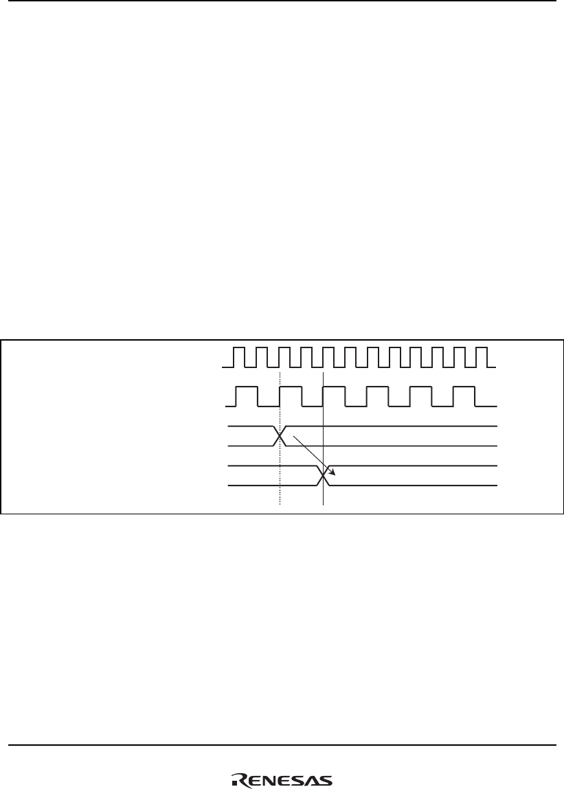
28. General Purpose I/O Ports (GPIO)
Rev.1.00 Jan. 10, 2008 Page 1449 of 1658
REJ09B0261-0100
28.3 Usage Example
Setting procedure examples are described below.
28.3.1 Port Output Function
To output the data of port data registers (PADR to PRDR) from the GPIO output port, write B'01
to the corresponding two bits in port control registers (PACR to PRCR).
In this case, for each output port, the settings of the port pull-up control registers (PEPUPR,
PHPUPR, PJPUPR, PKPUPR, PLPUPR, PMPUPR, and PNPUPR), peripheral module select
register 1 (P1MSELR), peripheral module select register 2 (P2MSELR), and bus mode pin
(MODE11 and MODE12) are invalid.
Figure 28.1 shows an example of operation timing diagram when port A is used as an output port.
The output data is written to port data registers (PADR to PRDR) and then the data is output via
the corresponding port pins after one peripheral clock (Pck).
CLKOUT
Peripheral clock (Pck)
Port A data register
PA7 to PA0
(D63/AD31 to D56/AD24)
Data
Data
Figure 28.1 Port A Data Output Timing Diagram
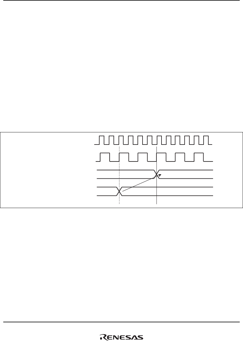
28. General Purpose I/O Ports (GPIO)
Rev.1.00 Jan. 10, 2008 Page 1450 of 1658
REJ09B0261-0100
28.3.2 Port Input function
To input the data via the GPIO port, write B'10 or B'11 to the corresponding two bits in port
control registers (PACR to PRCR). B’10 should be written when the pull-up MOS is off, and B'11
when the pull-up MOS is on. The input data to each port can be read out from the corresponding
bit in port data registers (PADR to PRCR).
In this case, for each input port, the settings of port pull-up control registers (PEPUPR, PHPUPR,
PJPUPR, PKPUPR, PLPUPR, PMPUPR, and PNPUPR), peripheral module select register 1
(P1MSELR), peripheral module select register 2 (P2MSELR), and bus-mode pin (MODE11 and
MODE12) are invalid.
Figure 28.2 shows an example of operation timing diagram when port A is used as an input port.
The input data from each port can be read out from corresponding port data register after the 2nd
rising edge of the peripheral clock (Pck).
CLKOUT
Peripheral clock (Pck)
Port A data register
PA7 to PA0
(D63/AD31 to D56/AD24)
Data
Data
Figure 28.2 Port A Data Input Timing Diagram

28. General Purpose I/O Ports (GPIO)
Rev.1.00 Jan. 10, 2008 Page 1451 of 1658
REJ09B0261-0100
28.3.3 Peripheral Module Function
The procedures for setting the peripheral module function are described below.
1. Select the peripheral module by using the peripheral module select register 1 (P1MSELR) and
peripheral module select register 2 (P2MSELR).
2. When an input or input/output pin is used, it is necessary to set the pull-up MOS for each pin
by using the port pull-up control registers (PEPUPR, PHPUPR, PJPUPR, PKPUPR. PLPUPR,
PMPUPR, and PNPUPR). Write B'0 (when the pull-up MOS is off ) or B'1 (when the pull-up
MOS is on) to the corresponding bit. When an output port is used, the pull-up MOS is off
regardless of the settings of the port pull-up control registers.
3. Write B'00 to the corresponding two bits in the port control registers (PACR to PRCR).

28. General Purpose I/O Ports (GPIO)
Rev.1.00 Jan. 10, 2008 Page 1452 of 1658
REJ09B0261-0100

29. User Break Controller (UBC)
Rev.1.00 Jan. 10, 2008 Page 1453 of 1658
REJ09B0261-0100
Section 29 User Break Controller (UBC)
The user break controller (UBC) provides versatile functions to facilitate program debugging.
These functions help to ease creation of a self-monitor/debugger, which allows easy program
debugging using this LSI alone, without using the in-circuit emulator. Various break conditions
can be set in the UBC: instruction fetch or read/write access of an operand, operand size, data
contents, address value, and program stop timing for instruction fetch.
29.1 Features
1. The following break conditions can be set.
Break channels: Two (channels 0 and 1)
User break conditions can be set independently for channels 0 and 1, and can also be set as a
single sequential condition for the two channels, that is, a sequential break. (Sequential break
involves two cases such that the channel 0 break condition is satisfied in a certain bus cycle
and then the channel 1 break condition is satisfied in a different bus cycle, and vice versa.)
• Address
When 40 bits containing ASID and 32-bit address are compared with the specified value, all
the ASID bits can be compared or masked.
32-bit address can be masked bit by bit, allowing the user to mask the address in desired page
sizes such as lower 12 bits (4-Kbyte page) and lower 10 bits (1-Kbyte page).
• Data
32 bits can be masked only for channel 1.
• Bus cycle
The program can break either for instruction fetch (PC break) or operand access.
• Read or write access
• Operand sizes
Byte, word, longword, and quadword are supported.
2. The user-designated exception handling routine for the user break condition can be executed.
3. Pre-instruction-execution or post-instruction-execution can be selected as the PC break timing.
4. A maximum of 212 – 1 repetition counts can be specified as the break condition (available only
for channel 1).
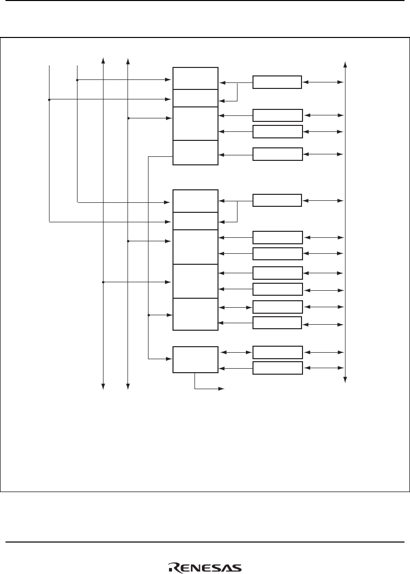
29. User Break Controller (UBC)
Rev.1.00 Jan. 10, 2008 Page 1454 of 1658
REJ09B0261-0100
Figure 29.1 shows the UBC block diagram.
SAB
Internal bus
Access
comparator
Address
comparator
Channel 0
operation
control
Channel 1
operation
control
Access
comparator
Address
comparator
Data
comparator
Control
CBR0
CAR0
CAMR0
CRR0
CBR1
CAR1
CAMR1
CDR1
CDMR1
CETR1
CRR1
CCMFR
CBCR
User break is requested.
SDB
Access
control
CBR0:
CRR0:
CAR0:
CAMR0:
CBR1:
CRR1:
CAR1:
CAMR1:
CDR1:
CDMR1:
CETR1:
CCMFR:
CBCR:
SAB:
SDB:
Legend:
ASID
comparator
ASID
comparator
ASID
Match condition setting register 0
Match operation setting register 0
Match address setting register 0
Match address mask setting register 0
Match condition setting register 1
Match operation setting register 1
Match address setting register 1
Match address mask setting register 1
Match data setting register 1
Match data mask setting register 1
Execution count break register
Channel match flag register
Break control register
Operand address bus
Operand data bus
Figure 29.1 Block Diagram of UBC

29. User Break Controller (UBC)
Rev.1.00 Jan. 10, 2008 Page 1455 of 1658
REJ09B0261-0100
29.2 Register Descriptions
The UBC has the following registers.
Table 29.1 Register Configuration
Name Abbreviation R/W P4 Address*
Area 7
Address*
Access
Size
Match condition setting
register 0
CBR0 R/W H'FF200000 H'1F200000 32
Match operation setting
register 0
CRR0 R/W H'FF200004 H'1F200004 32
Match address setting
register 0
CAR0 R/W H'FF200008 H'1F200008 32
Match address mask setting
register 0
CAMR0 R/W H'FF20000C H'1F20000C 32
Match condition setting
register 1
CBR1 R/W H'FF200020 H'1F200020 32
Match operation setting
register 1
CRR1 R/W H'FF200024 H'1F200024 32
Match address setting
register 1
CAR1 R/W H'FF200028 H'1F200028 32
Match address mask setting
register 1
CAMR1 R/W H'FF20002C H'1F20002C 32
Match data setting register 1 CDR1 R/W H'FF200030 H'1F200030 32
Match data mask setting
register 1
CDMR1 R/W H'FF200034 H'1F200034 32
Execution count break
register 1
CETR1 R/W H'FF200038 H'1F200038 32
Channel match flag register CCMFR R/W H'FF200600 H'1F200600 32
Break control register CBCR R/W H'FF200620 H'1F200620 32
Note: * P4 addresses are used when area P4 in the virtual address space is used, and area 7
addresses are used when accessing the register through area 7 in the physical address
space using the TLB.

29. User Break Controller (UBC)
Rev.1.00 Jan. 10, 2008 Page 1456 of 1658
REJ09B0261-0100
Table 29.2 Register Status in Each Processing State
Register Name Abbreviation Power-on Reset Manual Reset Sleep
Match condition setting
register 0
CBR0 H'20000000 Retained Retained
Match operation setting
register 0
CRR0 H'00002000 Retained Retained
Match address setting
register 0
CAR0 Undefined Retained Retained
Match address mask
setting register 0
CAMR0 Undefined Retained Retained
Match condition setting
register 1
CBR1 H'20000000 Retained Retained
Match operation setting
register 1
CRR1 H'00002000 Retained Retained
Match address setting
register 1
CAR1 Undefined Retained Retained
Match address mask
setting register 1
CAMR1 Undefined Retained Retained
Match data setting
register 1
CDR1 Undefined Retained Retained
Match data mask setting
register 1
CDMR1 Undefined Retained Retained
Execution count break
register 1
CETR1 Undefined Retained Retained
Channel match flag
register
CCMFR H'00000000 Retained Retained
Break control register CBCR H'00000000 Retained Retained
The access size must be the same as the control register size. If the size is different, the register is
not written to if attempted, and reading the register returns the undefined value. A desired break
may not occur between the time when the instruction for rewriting the control register is executed
and the time when the written value is actually reflected on the register. In order to confirm the
exact timing when the control register is updated, read the data which has been written most
recently. The subsequent instructions are valid for the most recently written register value.
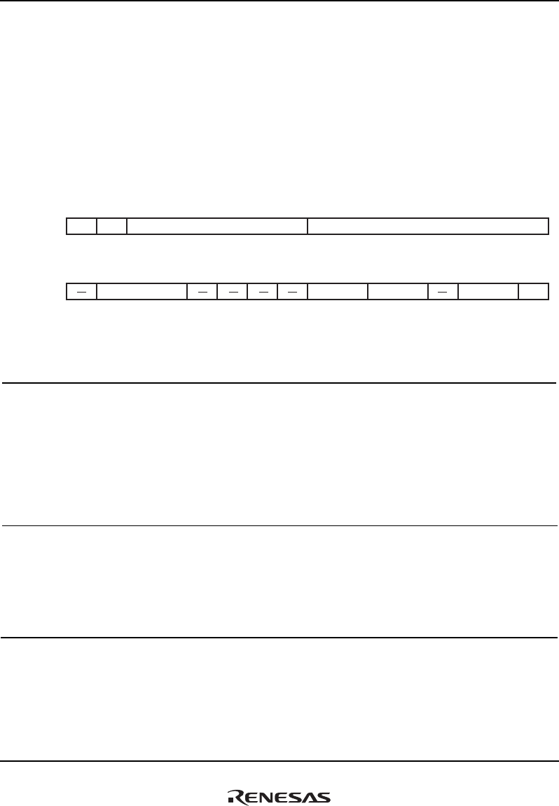
29. User Break Controller (UBC)
Rev.1.00 Jan. 10, 2008 Page 1457 of 1658
REJ09B0261-0100
29.2.1 Match Condition Setting Registers 0 and 1 (CBR0 and CBR1)
CBR0 and CBR1 are readable/writable 32-bit registers which specify the break conditions for
channels 0 and 1, respectively. The following break conditions can be set in the CBR0 and CBR1:
(1) whether or not to include the match flag in the conditions, (2) whether or not to include the
ASID, and the ASID value when included, (3) whether or not to include the data value, (4)
operand size, (5) whether or not to include the execution count, (6) bus type, (7) instruction fetch
cycle or operand access cycle, and (8) read or write access cycle.
• CBR0
31 30 29 28 27 26 25 24 23 22 21 20 19 18 17 16
0010000000000000
MFE AIE MFI AIV
SZ CD ID
RW CE
R/W R/W R/W R/W R/W R/W R/W R/W R/W R/W R/W R/W R/W R/W R/W R/W
15 14 13 12 11 10 9 8 7 6 5 4 3 2 1 0
0000000000000000
R R/W R/W R/W R R R R R/W R/W R/W R/W R R/W R/W R/W
Bit :
Initial value :
R/W:
Bit :
Initial value :
R/W:
Bit Bit Name
Initial
Value R/W Description
31 MFE 0 R/W Match Flag Enable
Specifies whether or not to include the match flag value
specified by the MFI bit of this register in the match
conditions. When the specified match flag value is 1, the
condition is determined to be satisfied.
0: The match flag is not included in the match conditions;
thus, not checked.
1: The match flag is included in the match conditions.
30 AIE 0 R/W ASID Enable
Specifies whether or not to include the ASID specified by
the AIV bit of this register in the match conditions.
0: The ASID is not included in the match conditions;
thus, not checked.
1: The ASID is included in the match conditions.

29. User Break Controller (UBC)
Rev.1.00 Jan. 10, 2008 Page 1458 of 1658
REJ09B0261-0100
Bit Bit Name
Initial
Value R/W Description
29 to 24 MFI 100000 R/W Match Flag Specify
Specifies the match flag to be included in the match
conditions.
000000: MF0 bit of the CCMFR register
000001: MF1 bit of the CCMFR register
Others: Reserved (setting prohibited)
Note: The initial value is the reserved value, but when 1
is written into CBR0[0], MFI must be set to 000000
or 000001. And note that the channel 0 is not hit
when MFE bit of this register is 1 and MFI bits are
000000 in the condition of CCRMF.MF0 = 0.
23 to 16 AIV All 0 R/W ASID Specify
Specifies the ASID value to be included in the match
conditions.
15 — 0 R Reserved
For read/write in this bit, refer to General Precautions on
Handling of Product.
14 to 12 SZ All 0 R/W Operand Size Select
Specifies the operand size to be included in the match
conditions. This bit is valid only when the operand
access cycle is specified as a match condition.
000: The operand size is not included in the match
conditions; thus, not checked (any operand size
specifies the match condition).*1
001: Byte access
010: Word access
011: Longword access
100: Quadword access*2
Others: Reserved (setting prohibited)
11 to 8 — All 0 R Reserved
For read/write in this bit, refer to General Precautions on
Handling of Product.

29. User Break Controller (UBC)
Rev.1.00 Jan. 10, 2008 Page 1459 of 1658
REJ09B0261-0100
Bit Bit Name
Initial
Value R/W Description
7, 6 CD All 0 R/W Bus Select
Specifies the bus to be included in the match conditions.
This bit is valid only when the operand access cycle is
specified as a match condition.
00: Operand bus for operand access
Others: Reserved (setting prohibited)
5, 4 ID All 0 R/W Instruction Fetch/Operand Access Select
Specifies the instruction fetch cycle or operand access
cycle as the match condition.
00: Instruction fetch cycle or operand access cycle
01: Instruction fetch cycle
10: Operand access cycle
11: Instruction fetch cycle or operand access cycle
3 — 0 R Reserved
For read/write in this bit, refer to General Precautions on
Handling of Product.
2, 1 RW All 0 R/W Bus Command Select
Specifies the read/write cycle as the match condition.
This bit is valid only when the operand access cycle is
specified as a match condition.
00: Read cycle or write cycle
01: Read cycle
10: Write cycle
11: Read cycle or write cycle
0 CE 0 R/W Channel Enable
Validates/invalidates the channel. If this bit is 0, all the
other bits of this register are invalid.
0: Invalidates the channel.
1: Validates the channel.
Notes: 1. If the data value is included in the match conditions, be sure to specify the operand
size.
2. If the quadword access is specified and the data value is included in the match
conditions, the upper and lower 32 bits of 64-bit data are each compared with the
contents of both the match data setting register and the match data mask setting
register.

29. User Break Controller (UBC)
Rev.1.00 Jan. 10, 2008 Page 1460 of 1658
REJ09B0261-0100
• CBR1
31 30 29 28 27 26 25 24 23 22 21 20 19 18 17 16
0010000000000000
MFE AIE MFI AIV
DBE SZ ETBE CD ID RW
CE
R/W R/W R/W R/W R/W R/W R/W R/W R/W R/W R/W R/W R/W R/W R/W R/W
15 14 13 12 11 10 9 8 7 6 5 4 3 2 1 0
0000000000000000
R/W R/W R/W R/W R/W R R R R/W R/W R/W R/W R R/W R/W R/W
Bit :
Initial value :
R/W:
Bit :
Initial value :
R/W:
Bit Bit Name
Initial
Value R/W Description
31 MFE 0 R/W Match Flag Enable
Specifies whether or not to include the match flag value
specified by the MFI bit of this register in the match
conditions. When the specified match flag value is 1,
the condition is determined to be satisfied.
0: The match flag is not included in the match
conditions; thus, not checked.
1: The match flag is included in the match conditions.
30 AIE 0 R/W ASID Enable
Specifies whether or not to include the ASID specified
by the AIV bit of this register in the match conditions.
0: The ASID is not included in the match conditions;
thus, not checked.
1: The ASID is included in the match conditions.
29 to 24 MFI 100000 R/W Match Flag Specify
Specifies the match flag to be included in the match
conditions.
000000: The MF0 bit of the CCMFR register
000001: The MF1 bit of the CCMFR register
Others: Reserved (setting prohibited)
Note: The initial value is the reserved value, but when 1
is written into CBR1[0], MFI must be set to
000000 or 000001. And note that the channel 1 is
not hit when MFE bit of this register is 1 and MFI
bits are 000001 in the condition of CCRMF.MF1 =
0.

29. User Break Controller (UBC)
Rev.1.00 Jan. 10, 2008 Page 1461 of 1658
REJ09B0261-0100
Bit Bit Name
Initial
Value R/W Description
23 to 16 AIV All 0 R/W ASID Specify
Specifies the ASID value to be included in the match
conditions.
15 DBE 0 R/W Data Value Enable*3
Specifies whether or not to include the data value in the
match condition. This bit is valid only when the operand
access cycle is specified as a match condition.
0: The data value is not included in the match
conditions; thus, not checked.
1: The data value is included in the match conditions.
14 to 12 SZ All 0 R/W Operand Size Select
Specifies the operand size to be included in the match
conditions. This bit is valid only when the operand
access cycle is specified as a match condition.
000: The operand size is not included in the match
condition; thus, not checked (any operand size
specifies the match condition). *1
001: Byte access
010: Word access
011: Longword access
100: Quadword access*2
Others: Reserved (setting prohibited)
11 ETBE 0 R/W Execution Count Value Enable
Specifies whether or not to include the execution count
value in the match conditions. If this bit is 1 and the
match condition satisfaction count matches the value
specified by the CETR1 register, the operation specified
by the CRR1 register is performed.
0: The execution count value is not included in the
match conditions; thus, not checked.
1: The execution count value is included in the match
conditions.
10 to 8 — All 0 R Reserved
For read/write in this bit, refer to General Precautions
on Handling of Product.

29. User Break Controller (UBC)
Rev.1.00 Jan. 10, 2008 Page 1462 of 1658
REJ09B0261-0100
Bit Bit Name
Initial
Value R/W Description
7, 6 CD All 0 R/W Bus Select
Specifies the bus to be included in the match
conditions. This bit is valid only when the operand
access cycle is specified as a match condition.
00: Operand bus for operand access
Others: Reserved (setting prohibited)
5, 4 ID All 0 R/W Instruction Fetch/Operand Access Select
Specifies the instruction fetch cycle or operand access
cycle as the match condition.
00: Instruction fetch cycle or operand access cycle
01: Instruction fetch cycle
10: Operand access cycle
11: Instruction fetch cycle or operand access cycle
3 — 0 R Reserved
For read/write in this bit, refer to General Precautions
on Handling of Product.
2, 1 RW All 0 R/W Bus Command Select
Specifies the read/write cycle as the match condition.
This bit is valid only when the operand access cycle is
specified as a match condition.
00: Read cycle or write cycle
01: Read cycle
10: Write cycle
11: Read cycle or write cycle
0 CE 0 R/W Channel Enable
Validates/invalidates the channel. If this bit is 0, all the
other bits in this register are invalid.
0: Invalidates the channel.
1: Validates the channel.
Notes: 1. If the data value is included in the match conditions, be sure to specify the operand
size.
2. If the quadword access is specified and the data value is included in the match
conditions, the upper and lower 32 bits of 64-bit data are each compared with the
contents of both the match data setting register and the match data mask setting
register.
3. The OCBI instruction is handled as longword write access without the data value, and
the PREF, OCBP, and OCBWB instructions are handled as longword read access
without the data value. Therefore, do not include the data value in the match conditions
for these instructions.
29. User Break Controller (UBC)
Rev.1.00 Jan. 10, 2008 Page 1463 of 1658
REJ09B0261-0100
29.2.2 Match Operation Setting Registers 0 and 1 (CRR0 and CRR1)
CRR0 and CRR1 are readable/writable 32-bit registers which specify the operation to be executed
when channels 0 and 1 satisfy the match condition, respectively. The following operations can be
set in the CRR0 and CRR1 registers: (1) breaking at a desired timing for the instruction fetch cycle
and (2) requesting a break.
• CRR0
31 30 29 28 27 26 25 24 23 22 21 20 19 18 17 16
0000000000000000
PCB BIE
RRRRRRRRRRRRRRRR
15 14 13 12 11 10 9 8 7 6 5 4 3 2 1 0
0010000000000000
RRRRRRRRRRRRRRR/WR/W
Bit :
Initial value :
R/W:
Bit :
Initial value :
R/W:
Bit Bit Name
Initial
Value R/W Description
31 to 14 — All 0 R Reserved
For read/write in this bit, refer to General Precautions
on Handling of Product.
13 — 1 R Reserved
This bit is always read as 1. The write value should
always be 1.
12 to 2 — All 0 R Reserved
For read/write in this bit, refer to General Precautions
on Handling of Product.
1 PCB 0 R/W PC Break Select
Specifies either before or after instruction execution as
the break timing for the instruction fetch cycle. This bit
is invalid for breaks other than the ones for the
instruction fetch cycle.
0: Sets the PC break before instruction execution.
1: Sets the PC break after instruction execution.
0 BIE 0 R/W Break Enable
Specifies whether or not to request a break when the
match condition is satisfied for the channel.
0: Does not request a break.
1: Requests a break.

29. User Break Controller (UBC)
Rev.1.00 Jan. 10, 2008 Page 1464 of 1658
REJ09B0261-0100
• CRR1
31 30 29 28 27 26 25 24 23 22 21 20 19 18 17 16
0000000000000000
PCB BIE
RRRRRRRRRRRRRRRR
15 14 13 12 11 10 9 8 7 6 5 4 3 2 1 0
0010000000000000
RRRRRRRRRRRRRRR/WR/W
Bit :
Initial value :
R/W:
Bit :
Initial value :
R/W:
Bit Bit Name
Initial
Value R/W Description
31 to 14 — All 0 R Reserved
For read/write in this bit, refer to General Precautions
on Handling of Product.
13 — 1 R Reserved
This bit is always read as 1. The write value should
always be 1.
12 to 2 — All 0 R Reserved
For read/write in this bit, refer to General Precautions
on Handling of Product.
1 PCB 0 R/W PC Break Select
Specifies either before or after instruction execution as
the break timing for the instruction fetch cycle. This bit
is invalid for breaks other than ones for the instruction
fetch cycle.
0: Sets the PC break before instruction execution.
1: Sets the PC break after instruction execution.
0 BIE 0 R/W Break Enable
Specifies whether or not to request a break when the
match condition is satisfied for the channel.
0: Does not request a break.
1: Requests a break.
29. User Break Controller (UBC)
Rev.1.00 Jan. 10, 2008 Page 1465 of 1658
REJ09B0261-0100
29.2.3 Match Address Setting Registers 0 and 1 (CAR0 and CAR1)
CAR0 and CAR1 are readable/writable 32-bit registers specifying the virtual address to be
included in the break conditions for channels 0 and 1, respectively.
• CAR0
31 30 29 28 27 26 25 24 23 22 21 20 19 18 17 16
CA
CA
R/W R/W R/W R/W R/W R/W R/W R/W R/W R/W R/W R/W R/W R/W R/W R/W
15 14 13 12 11 10 9 8 7 6 5 4 3 2 1 0
R/W R/W R/W R/W R/W R/W R/W R/W R/W R/W R/W R/W R/W R/W R/W R/W
Bit :
Initial value :
R/W:
Bit :
Initial value :
R/W:
Bit Bit Name
Initial
Value R/W Description
31 to 0 CA Undefined R/W Compare Address
Specifies the address to be included in the break
conditions.
When the operand bus has been specified using the
CBR0 register, specify the SAB address in CA[31:0].
• CAR1
31 30 29 28 27 26 25 24 23 22 21 20 19 18 17 16
CA
CA
R/W R/W R/W R/W R/W R/W R/W R/W R/W R/W R/W R/W R/W R/W R/W R/W
15 14 13 12 11 10 9 8 7 6 5 4 3 2 1 0
R/W R/W R/W R/W R/W R/W R/W R/W R/W R/W R/W R/W R/W R/W R/W R/W
Bit :
Initial value :
R/W:
Bit :
Initial value :
R/W:
Bit Bit Name
Initial
Value R/W Description
31 to 0 CA Undefined R/W Compare Address
Specifies the address to be included in the break
conditions.
When the operand bus has been specified using the
CBR1 register, specify the SAB address in CA[31:0].

29. User Break Controller (UBC)
Rev.1.00 Jan. 10, 2008 Page 1466 of 1658
REJ09B0261-0100
29.2.4 Match Address Mask Setting Registers 0 and 1 (CAMR0 and CAMR1)
CMAR0 and CMAR1 are readable/writable 32-bit registers which specify the bits to be masked
among the address bits specified by using the match address setting register of the corresponding
channel. (Set the bits to be masked to 1.)
• CAMR0
31 30 29 28 27 26 25 24 23 22 21 20 19 18 17 16
CAM
CAM
R/W R/W R/W R/W R/W R/W R/W R/W R/W R/W R/W R/W R/W R/W R/W R/W
15 14 13 12 11 10 9 8 7 6 5 4 3 2 1 0
R/W R/W R/W R/W R/W R/W R/W R/W R/W R/W R/W R/W R/W R/W R/W R/W
Bit :
Initial value :
R/W:
Bit :
Initial value :
R/W:
Bit Bit Name
Initial
Value R/W Description
31 to 0 CAM Undefined R/W Compare Address Mask
Specifies the bits to be masked among the address
bits which are specified using the CAR0 register. (Set
the bits to be masked to 1.)
0: Address bits CA[n] are included in the break
condition.
1: Address bits CA[n] are masked and not included in
the break condition.
[n] = any values from 31 to 0

29. User Break Controller (UBC)
Rev.1.00 Jan. 10, 2008 Page 1467 of 1658
REJ09B0261-0100
• CAMR1
31 30 29 28 27 26 25 24 23 22 21 20 19 18 17 16
CAM
CAM
R/W R/W R/W R/W R/W R/W R/W R/W R/W R/W R/W R/W R/W R/W R/W R/W
15 14 13 12 11 10 9 8 7 6 5 4 3 2 1 0
R/W R/W R/W R/W R/W R/W R/W R/W R/W R/W R/W R/W R/W R/W R/W R/W
Bit :
Initial value :
R/W:
Bit :
Initial value :
R/W:
Bit Bit Name
Initial
Value R/W Description
31 to 0 CAM Undefined R/W Compare Address Mask
Specifies the bits to be masked among the address
bits which are specified using the CAR1 register. (Set
the bits to be masked to 1.)
0: Address bits CA[n] are included in the break
condition.
1: Address bits CA[n] are masked and not included in
the break condition.
[n] = any values from 31 to 0

29. User Break Controller (UBC)
Rev.1.00 Jan. 10, 2008 Page 1468 of 1658
REJ09B0261-0100
29.2.5 Match Data Setting Register 1 (CDR1)
CDR1 is a readable/writable 32-bit register which specifies the data value to be included in the
break conditions for channel 1.
31 30 29 28 27 26 25 24 23 22 21 20 19 18 17 16
CD
CD
R/W R/W R/W R/W R/W R/W R/W R/W R/W R/W R/W R/W R/W R/W R/W R/W
15 14 13 12 11 10 9 8 7 6 5 4 3 2 1 0
R/W R/W R/W R/W R/W R/W R/W R/W R/W R/W R/W R/W R/W R/W R/W R/W
Bit :
Initial value :
R/W:
Bit :
Initial value :
R/W:
Bit Bit Name
Initial
Value R/W Description
31 to 0 CD Undefined R/W Compare Data Value
Specifies the data value to be included in the break
conditions.
When the operand bus has been specified using the
CBR1 register, specify the SDB data value in CD[31:0].
Table 29.3 Settings for Match Data Setting Register
Bus and Size Selected
Using CBR1 CD[31:24] CD[23:16] CD[15:8] CD[7:0]
Operand bus (byte) Don't care Don't care Don't care SDB7 to SDB0
Operand bus (word) Don't care Don't care SDB15 to SDB8 SDB7 to SDB0
Operand bus (longword) SDB31 to SDB24 SDB23 to SDB16 SDB15 to SDB8 SDB7 to SDB0
Notes: 1. If the data value is included in the match conditions, be sure to specify the operand
size.
2. The OCBI instruction is handled as longword write access without the data value, and
the PREF, OCBP, and OCBWB instructions are handled as longword read access
without the data value. Therefore, do not include the data value in the match conditions
for these instructions.
3. If the quadword access is specified and the data value is included in the match
conditions, the upper and lower 32 bits of 64-bit data are each compared with the
contents of both the match data setting register and match data mask setting register.

29. User Break Controller (UBC)
Rev.1.00 Jan. 10, 2008 Page 1469 of 1658
REJ09B0261-0100
29.2.6 Match Data Mask Setting Register 1 (CDMR1)
CDMR1 is a readable/writable 32-bit register which specifies the bits to be masked among the
data value bits specified using the match data setting register. (Set the bits to be masked to 1.)
31 30 29 28 27 26 25 24 23 22 21 20 19 18 17 16
CDM
CDM
R/W R/W R/W R/W R/W R/W R/W R/W R/W R/W R/W R/W R/W R/W R/W R/W
15 14 13 12 11 10 9 8 7 6 5 4 3 2 1 0
R/W R/W R/W R/W R/W R/W R/W R/W R/W R/W R/W R/W R/W R/W R/W R/W
Bit :
Initial value :
R/W:
Bit :
Initial value :
R/W:
Bit Bit Name
Initial
Value R/W Description
31 to 0 CDM Undefined R/W Compare Data Value Mask
Specifies the bits to be masked among the data value
bits specified using the CDR1 register. (Set the bits to
be masked to 1.)
0: Data value bits CD[n] are included in the break
condition.
1: Data value bits CD[n] are masked and not included
in the break condition.
[n] = any values from 31 to 0
29. User Break Controller (UBC)
Rev.1.00 Jan. 10, 2008 Page 1470 of 1658
REJ09B0261-0100
29.2.7 Execution Count Break Register 1 (CETR1)
CETR1 is a readable/writable 32-bit register which specifies the number of the channel hits before
a break occurs. A maximum value of 212 – 1 can be specified. When the execution count value is
included in the match conditions by using the match condition setting register, the value of this
register is decremented by one every time the channel is hit. When the channel is hit after the
register value reaches H'001, a break occurs.
31 30 29 28 27 26 25 24 23 22 21 20 19 18 17 16
0000000000000000
CET
RRRRRRRRRRRRRRRR
15 14 13 12 11 10 9 8 7 6 5 4 3 2 1 0
0000
R R R R R/W R/W R/W R/W R/W R/W R/W R/W R/W R/W R/W R/W
Bit :
Initial value :
R/W:
Bit :
Initial value :
R/W:
Bit Bit Name
Initial
Value
R/W
Description
31 to 12 — All 0 R Reserved
For read/write in this bit, refer to General Precautions on
Handling of Product.
11 to 0 CET Undefined R/W Execution Count
Specifies the execution count to be included in the break
conditions.

29. User Break Controller (UBC)
Rev.1.00 Jan. 10, 2008 Page 1471 of 1658
REJ09B0261-0100
29.2.8 Channel Match Flag Register (CCMFR)
CCMFR is a readable/writable 32-bit register which indicates whether or not the match conditions
have been satisfied for each channel. When a channel match condition has been satisfied, the
corresponding flag bit is set to 1. To clear the flags, write the data containing value 0 for the bits to
be cleared and value 1 for the other bits to this register. (The logical AND between the value
which has been written and the current register value is actually written to the register.) Sequential
operation using multiple channels is available by using these match flags.
31 30 29 28 27 26 25 24 23 22 21 20 19 18 17 16
0000000000000000
MF1 MF0
RRRRRRRRRRRRRRRR
15 14 13 12 11 10 9 8 7 6 5 4 3 2 1 0
0000000000000000
RRRRRRRRRRRRRRR/WR/W
Bit :
Initial value :
R/W:
Bit :
Initial value :
R/W:
Bit Bit Name
Initial
Value R/W Description
31 to 2 — All 0 R Reserved
For read/write in this bit, refer to General Precautions
on Handling of Product.
1 MF1 0 R/W Channel 1 Condition Match Flag
This flag is set to 1 when the channel 1 match
condition has been satisfied. To clear the flag, write 0
to this bit.
0: Channel 1 match condition has not been satisfied.
1: Channel 1 match condition has been satisfied.
0 MF0 0 R/W Channel 0 Condition Match Flag
This flag is set to 1 when the channel 0 match
condition has been satisfied. To clear the flag, write 0
to this bit.
0: Channel 0 match condition has not been satisfied.
1: Channel 0 match condition has been satisfied.

29. User Break Controller (UBC)
Rev.1.00 Jan. 10, 2008 Page 1472 of 1658
REJ09B0261-0100
29.2.9 Break Control Register (CBCR)
CBCR is a readable/writable 32-bit register which specifies whether or not to use the user break
debugging support function. For details on the user break debugging support function, refer to
section 29.4, User Break Debugging Support Function.
31 30 29 28 27 26 25 24 23 22 21 20 19 18 17 16
0000000000000000
UBDE
RRRRRRRRRRRRRRRR
15 14 13 12 11 10 9 8 7 6 5 4 3 2 1 0
0000000000000000
RRRRRRRRRRRRRRRR/W
Bit :
Initial value :
R/W:
Bit :
Initial value :
R/W:
Bit Bit Name
Initial
Value R/W Description
31 to 1 — All 0 R Reserved
For read/write in this bit, refer to General Precautions on
Handling of Product.
0 UBDE 0 R/W User Break Debugging Support Function Enable
Specifies whether or not to use the user break debugging
support function.
0: Does not use the user break debugging support
function.
1: Uses the user break debugging support function.

29. User Break Controller (UBC)
Rev.1.00 Jan. 10, 2008 Page 1473 of 1658
REJ09B0261-0100
29.3 Operation Description
29.3.1 Definition of Words Related to Accesses
"Instruction fetch" refers to an access in which an instruction is fetched. For example, fetching the
instruction located at the branch destination after executing a branch instruction is an instruction
access. "Operand access" refers to any memory access accompanying execution of an instruction.
For example, accessing an address (PC + disp × 2 + 4) in the instruction MOV.W@(disp,PC),Rn
is an operand access. "Data" is used in contrast to "address".
All types of operand access are classified into read or write access. Special care must be taken in
using the following instructions.
• PREF, OCBP, and OCBWB: Instructions for a read access
• MOVCA.L and OCBI: Instructions for a write access
• TAS.B: Instruction for a single read access or a single write access
The operand access accompanying the PREF, OCBP, OCBWB, and OCBI instructions is access
without the data value; therefore, do not include the data value in the match conditions for these
instructions.
The operand size should be defined for all types of operand access. Available operand sizes are
byte, word, longword, and quadword. For operand access accompanying the PREF, OCBP,
OCBWB, MOVCA.L, and OCBI instructions, the operand size is defined as longword.

29. User Break Controller (UBC)
Rev.1.00 Jan. 10, 2008 Page 1474 of 1658
REJ09B0261-0100
29.3.2 User Break Operation Sequence
The following describes the sequence from when the break condition is set until the user break
exception handling is initiated.
1. Specify the operand size, bus, instruction fetch/operand access, and read/write as the match
conditions using the match condition setting register (CBR0 or CBR1). Specify the break
address using the match address setting register (CAR0 or CAR1), and specify the address
mask condition using the match address mask setting register (CAMR0 or CAMR1). To
include the ASID in the match conditions, set the AIE bit in the match condition setting
register and specify the ASID value by the AIV bit in the same register. To include the data
value in the match conditions, set the DBE bit in the match condition setting register; specify
the break data using the match data setting register (CDR1); and specify the data mask
condition using the match data mask setting register (CDMR1). To include the execution count
in the match conditions, set the ETBE bit of the match condition setting register; and specify
the execution count using the execution count break register (CETR1). To use the sequential
break, set the MFE bit of the match condition setting register; and specify the number of the
first channel using the MFI bit.
2. Specify whether or not to request a break when the match condition is satisfied and the break
timing when the match condition is satisfied as a result of fetching the instruction using the
match operation setting register (CRR0 or CRR1). After having set all the bits in the match
condition setting register except the CE bit and the other necessary registers, set the CE bit and
read the match condition setting register again. This ensures that the set values in the control
registers are valid for the subsequent instructions immediately after reading the register.
Setting the CE bit of the match condition setting register in the initial state after reset via the
control registers may cause an undesired break.
3. When the match condition has been satisfied, the corresponding condition match flag (MF1 or
MF0) in the channel match flag register (CCMFR) is set. A break is also requested to the CPU
according to the set values in the match operation setting register (CRR0 or CRR1). The CPU
operates differently according to the BL bit value of the SR register: when the BL bit is 0, the
CPU accepts the break request and executes the specified exception handling; and when the
BL bit is 1, the CPU does not execute the exception handling.
4. The match flags (MF1 and MF0) can be used to confirm whether or not the corresponding
match condition has been satisfied. Although the flag is set when the condition is satisfied, it is
not cleared automatically; therefore, write 0 to the flag bit by issuing a memory store
instruction to the channel match flag register (CCMFR) in order to use the flag again.
5. Breaks may occur virtually at the same time for channels 0 and 1. In this case, only one break
request is sent to the CPU; however, the two condition match flags corresponding to these
breaks may be set.

29. User Break Controller (UBC)
Rev.1.00 Jan. 10, 2008 Page 1475 of 1658
REJ09B0261-0100
6. While the BL bit in the SR register is 1, no break requests are accepted. However, whether or
not the condition has been satisfied is determined. When the condition is determined to be
satisfied, the corresponding condition match flag is set.
7. If the sequential break conditions are set, the condition match flag is set every time the match
conditions are satisfied for each channel. When the conditions have been satisfied for the first
channel in the sequence but not for the second channel in the sequence, clear the condition
match flag for the first channel in the sequence in order to release the first channel in the
sequence from the match state.
29.3.3 Instruction Fetch Cycle Break
1. If the instruction fetch cycle is set in the match condition setting register (CBR0 or CBR1), the
instruction fetch cycle is handled as a match condition. To request a break upon satisfying the
match condition, set the BIE bit in the match operation setting register (CRR0 or CRR1) of the
corresponding channel. Either before or after executing the instruction can be selected as the
break timing according to the PCB bit value. If the instruction fetch cycle is specified as a
match condition, be sure to clear the LSB to 0 in the match address setting register (CAR0 or
CAR1); otherwise, no break occurs.
2. If pre-instruction-execution break is specified for the instruction fetch cycle, the break is
requested when the instruction is fetched and determined to be executed. Therefore, this
function cannot be used for the instructions which are fetched through overrun (i.e., the
instructions fetched during branching or making transition to the interrupt routine but not
executed). For priorities of pre-instruction-execution break and the other exceptions, refer to
section 5, Exception Handling. If pre-instruction-execution break is specified for the delayed
slot of the delayed branch instruction, the break is requested before the delayed branch
instruction is executed. However, do not specify pre-instruction-execution break for the
delayed slot of the RTE instruction.
3. If post-instruction-execution break is specified for the instruction fetch cycle, the break is
requested after the instruction which satisfied the match condition has been executed and
before the next instruction is executed. Similar to pre-instruction-execution break, this function
cannot be used for the instructions which are fetched through overrun. For priorities of post-
instruction-execution break and the other exceptions, refer to section 5, Exception Handling. If
post-instruction-execution break is specified for the delayed branch instruction and its delayed
slot, the break does not occur until the first instruction at the branch destination.
4. If the instruction fetch cycle is specified as the channel 1 match condition, the DBE bit of
match condition setting register CBR1 becomes invalid, the settings of match data setting
register CDR1 and match data mask setting register CDMR1 are ignored. Therefore, the data
value cannot be specified for the instruction fetch cycle break.

29. User Break Controller (UBC)
Rev.1.00 Jan. 10, 2008 Page 1476 of 1658
REJ09B0261-0100
29.3.4 Operand Access Cycle Break
1. Table 29.4 shows the relation between the operand sizes specified using the match condition
setting register (CBR0 or CBR1) and the address bits to be compared for the operand access
cycle break.
Table 29.4 Relation between Operand Sizes and Address Bits to Be Compared
Selected Operand Size Address Bits to be Compared
Quadword Address bits A31 to A3
Longword Address bits A31 to A2
Word Address bits A31 to A1
Byte Address bits A31 to A0
Operand size is not included in the
match conditions
Address bits A31 to A3 for quadword access
Address bits A31 to A2 for longword access
Address bits A31 to A1 for word access
Address bits A31 to A0 for byte access
The above table means that if address H'00001003 is set in the match address setting register
(CAR0 or CAR1), for example, the match condition is satisfied for the following access cycles
(assuming that all the other conditions are satisfied):
⎯ Longword access to address H'00001000
⎯ Word access to address H'00001002
⎯ Byte access to address H'00001003
2. When the data value is included in the channel 1 match conditions:
If the data value is included in the match conditions, be sure to select the quadword, longword,
word, or byte as the operand size using the operand size select bit (SZ) of the match condition
setting register (CBR1), and also set the match data setting register (CDR1) and the match data
mask setting register (CDMR1). With these settings, the match condition is satisfied when both
of the address and data conditions are satisfied. The data value and mask control for byte
access, word access, and longword access should be set in bits 7 to 0, 15 to 0, and 31 to 0 in
the bits CDR1 and CDMR1, respectively. For quadword access, 64-bit data is divided into the
upper and lower 32-bit data units, and each unit is independently compared with the specified
condition. When either the upper or lower 32-bit data unit satisfies the match condition, the
match condition for the 64-bit data is determined to be satisfied.
3. The operand access accompanying the PREF, OCBP, OCBWB, and OCBI instructions are
access without the data value; therefore, if the data value is included in the match conditions
for these instructions, the match conditions will never be satisfied.

29. User Break Controller (UBC)
Rev.1.00 Jan. 10, 2008 Page 1477 of 1658
REJ09B0261-0100
4. If the operand bus is selected, a break occurs after executing the instruction which has satisfied
the conditions and immediately before executing the next instruction. However, if the data
value is included in the match conditions, a break may occur after executing several
instructions after the instruction which has satisfied the conditions; therefore, it is impossible
to identify the instruction causing the break. If such a break has occurred for the delayed
branch instruction or its delayed slot, the break does not occur until the first instruction at the
branch destination.
However, do not specify the operand break for the delayed slot of the RTE instruction. And if
the data value is included in the match conditions, it is not allowed to set the break for the
preceding the RTE instruction by one to six instructions.
29.3.5 Sequential Break
1. Sequential break conditions can be specified by setting the MFE and MFI bits in the match
condition setting registers (CBR0 and CBR1). (Sequential break involves two cases such that
channel 0 break condition is satisfied then channel 1 break condition is satisfied, and vice
versa.) To use the sequential break function, clear the MFE bit of the match condition setting
register and the BIE bit of the match operation setting register of the first channel in the
sequence, and set the MFE bit and specify the number of the second channel in the sequence
using the MFI bit in the match condition setting register of the second channel in the sequence.
If the sequential break condition is set, the condition match flag is set every time the match
condition is satisfied for each channel. When the condition has been satisfied for the first
channel in the sequence but not for the second channel in the sequence, clear the condition
match flag for the first channel in the sequence in order to release the first channel in the
sequence from the match state.
2. For channel 1, the execution count break condition can also be included in the sequential break
conditions.
3. If the match conditions for the first and second channels in the sequence are satisfied within a
significantly short time, sequential operation may not be guaranteed in some cases, as shown
below.
• When the Match Condition is Satisfied at the Instruction Fetch Cycle for Both the First and
Second Channels in the Sequence:
Instruction B is 0 instruction after instruction A Equivalent to setting the same addresses; do
not use this setting.
Instruction B is one instruction after instruction A Sequential operation is not guaranteed.
Instruction B is two or more instructions after
instruction A
Sequential operation is guaranteed.

29. User Break Controller (UBC)
Rev.1.00 Jan. 10, 2008 Page 1478 of 1658
REJ09B0261-0100
• When the match condition is satisfied at the instruction fetch cycle for the first channel in the
sequence whereas the match condition is satisfied at the operand access cycle for the second
channel in the sequence:
Instruction B is 0 or one instruction after
instruction A
Sequential operation is not guaranteed.
Instruction B is two or more instructions after
instruction A
Sequential operation is guaranteed.
• When the match condition is satisfied at the operand access cycle for the first channel in the
sequence whereas the match condition is satisfied at the instruction fetch cycle for the second
channel in the sequence:
Instruction B is 0 to five instructions after
instruction A
Sequential operation is not guaranteed.
Instruction B is six or more instructions after
instruction A
Sequential operation is guaranteed.
• When the match condition is satisfied at the operand access cycle for both the first and second
channels in the sequence:
Instruction B is 0 to five instructions after
instruction A
Sequential operation is not guaranteed.
Instruction B is six or more instructions after
instruction A
Sequential operation is guaranteed.

29. User Break Controller (UBC)
Rev.1.00 Jan. 10, 2008 Page 1479 of 1658
REJ09B0261-0100
29.3.6 Program Counter Value to be Saved
When a break has occurred, the address of the instruction to be executed when the program
restarts is saved in the SPC then the exception handling state is initiated. A unique instruction
causing a break can be identified unless the data value is included in the match conditions.
1. When the instruction fetch cycle (before instruction execution) is specified as the match
condition:
The address of the instruction which has satisfied the match conditions is saved in the SPC.
The instruction which has satisfied the match conditions is not executed, but a break occurs
instead. However, if the match conditions are satisfied for the delayed slot instruction, the
address of the delayed branch instruction is saved in the SPC.
2. When the instruction fetch cycle (after instruction execution) is specified as the match
condition:
The address of the instruction immediately after the instruction which has satisfied the match
conditions is saved in the SPC. The instruction which has satisfied the match conditions is
executed, then a break occurs before the next instruction. If the match conditions are satisfied
for the delayed branch instruction or its delayed slot, these instructions are executed and the
address of the branch destination is saved in the SPC.
3. When the operand access (address only) is specified as the match condition:
The address of the instruction immediately after the instruction which has satisfied the break
conditions is saved in the SPC. The instruction which has satisfied the match conditions are
executed, then a break occurs before the next instruction. However, if the conditions are
satisfied for the delayed slot, the address of the branch destination is saved in the SPC.
4. When the operand access (address and data) is specified as the match condition:
If the data value is added to the match conditions, the instruction which has satisfied the match
conditions is executed. A user break occurs before executing an instruction that is one through
six instructions after the instruction which has satisfied the match conditions. The address of
the instruction is saved in the SPC; thus, it is impossible to identify exactly where a break will
occur. If the conditions are satisfied for the delayed slot instruction, the address of the branch
destination is saved in the SPC. If a branch instruction follows the instruction which has
satisfied the match conditions, a break may occur after the delayed instruction and delayed slot
are executed. In this case, the address of the branch destination is also saved in the SPC.
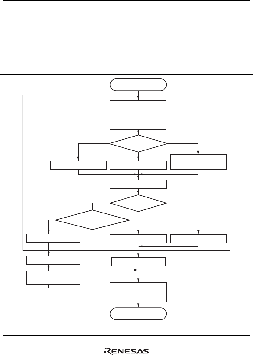
29. User Break Controller (UBC)
Rev.1.00 Jan. 10, 2008 Page 1480 of 1658
REJ09B0261-0100
29.4 User Break Debugging Support Function
By using the user break debugging support function, the branch destination address can be
modified when the CPU accepts the user break request. Specifically, setting the UBDE bit of
break control register CBCR to 1 allows branching to the address indicated by DBR instead of
branching to the address indicated by the [VBR + offset]. Figure 29.2 shows the flowchart of the
user break debugging support function.
SPC ← PC
SSR ← SR
SR.BL ← B'1
SR.MD ← B'1
SR.RB ← B'1
Exception/interrupt
is generated
Exception Exception/interrupt/trap? Tra p
Interrupt
PC ← H'A000 0000PC ← VBR + vector offset
Execute RTE instruction
PC ← SPC
SR ← SSR
SGR ← R15
PC ← DBR
Debugging program
R15 ← SGR
(STC instruction)
Reset exception?
(CBCR.UBDE == 1)
&& (user break)?
Exception operation ends
INTEVT ← Interrupt code
EXPEVT ← Exception code
YesNo
No
Yes
Hardware operations
Exception handling routine
TRA ← TRAPA (imm)
EXPEVT ← H'160
Figure 29.2 Flowchart of User Break Debugging Support Function

29. User Break Controller (UBC)
Rev.1.00 Jan. 10, 2008 Page 1481 of 1658
REJ09B0261-0100
29.5 User Break Examples
(1) Match Conditions Are Specified for an Instruction Fetch Cycle
• Example 1-1
Register settings: CBR0 = H'00000013 / CRR0 = H'00002003 / CAR0 = H'00000404 /
CAMR0 = H'00000000 / CBR1 = H'00000013 / CRR1 = H'00002001 / CAR1 = H'00008010 /
CAMR1 = H'00000006 / CDR1 = H'00000000 / CDMR1 = H'00000000 / CETR1 =
H'00000000 / CBCR = H'00000000
Specified conditions: Independent for channels 0 and 1
⎯ Channel 0
Address: H'00000404 / Address mask: H'00000000
Bus cycle: Instruction fetch (after executing the instruction)
ASID is not included in the conditions.
⎯ Channel 1:
Address: H'00008010 / Address mask: H'00000006
Data: H'00000000 / Data mask: H'00000000 / Execution count: H'00000000
Bus cycle: Instruction fetch (before executing instruction)
ASID, data values, and execution count are not included in the conditions.
With the above settings, the user break occurs after executing the instruction at address
H'00000404 or before executing the instruction at address H'00008010 to H'00008016.
• Example 1-2
Register settings: CBR0 = H'40800013 / CRR0 = H'00002000 / CAR0 = H'00037226 /
CAMR0 = H'00000000 / CBR1 = H'C0700013 / CRR1 = H'00002001 / CAR1 = H'0003722E /
CAMR1 = H'00000000 / CDR1 = H'00000000 / CDMR1 = H'00000000 / CETR1 =
H'00000000 / CBCR = H'00000000
Specified conditions: Channel 0 → Channel1 sequential mode
⎯ Channel 0
Address: H'00037226 / Address mask: H'00000000 / ASID: H'80
Bus cycle: Instruction fetch (before executing the instruction)
⎯ Channel 1
Address: H'0003722E / Address mask: H'00000000 / ASID: H'70
Data: H'00000000 / Data mask: H'00000000 / Execution count: H'00000000
Bus cycle: Instruction fetch (before executing the instruction)
Data values and execution count are not included in the conditions.

29. User Break Controller (UBC)
Rev.1.00 Jan. 10, 2008 Page 1482 of 1658
REJ09B0261-0100
With the above settings, the user break occurs after executing the instruction at address
H'00037226 where ASID is H'80 before executing the instruction at address H'0003722E
where ASID is H'70.
• Example 1-3
Register settings: CBR0 = H'00000013 / CRR0 = H'00002001 / CAR0 = H'00027128 /
CAMR0 = H'00000000 / CBR1 = H'00000013 / CRR1 = H'00002001 / CAR1 = H'00031415 /
CAMR1 = H'00000000 / CDR1 = H'00000000 / CDMR1 = H'00000000 / CETR1 =
H'00000000 / CBCR = H'00000000
Specified conditions: Independent for channels 0 and 1
⎯ Channel 0
Address: H'00027128 / Address mask: H'00000000
Bus cycle: Instruction fetch (before executing the instruction)
ASID is not included in the conditions.
⎯ Channel 1
Address: H'00031415 / Address mask: H'00000000
Data: H'00000000 / Data mask: H'00000000 / Execution count: H'00000000
Bus cycle: Instruction fetch (before executing the instruction)
ASID, data values, and execution count are not included in the conditions.
With the above settings, the user break occurs for channel 0 before executing the instruction at
address H'00027128. No user break occurs for channel 1 since the instruction fetch is executed
only at even addresses.
• Example 1-4
Register settings: CBR0 = H'40800013 / CRR0 = H'00002000 / CAR0 = H'00037226 /
CAMR0 = H'00000000 / CBR1 = H'C0700013 / CRR1 = H'00002001 / CAR1 = H'0003722E /
CAMR1 = H'00000000 / CDR1 = H'00000000 / CDMR1 = H'00000000 / CETR1 =
H'00000000 / CBCR = H'00000000
Specified conditions: Channel 0 → Channel 1 sequential mode
⎯ Channel 0
Address: H'00037226 / Address mask: H'00000000 / ASID: H'80
Bus cycle: Instruction fetch (before executing the instruction)
⎯ Channel 1
Address: H'0003722E / Address mask: H'00000000 / ASID: H'70
Data: H'00000000 / Data mask: H'00000000 / Execution count: H'00000000
Bus cycle: Instruction fetch (before executing the instruction)
Data values and execution count are not included in the conditions.

29. User Break Controller (UBC)
Rev.1.00 Jan. 10, 2008 Page 1483 of 1658
REJ09B0261-0100
With the above settings, the user break occurs after executing the instruction at address
H'00037226 where ASID is H'80 and before executing the instruction at address H'0003722E
where ASID is H'70.
• Example 1-5
Register settings: CBR0 = H'00000013 / CRR0 = H'00002001 / CAR0 = H'00000500 /
CAMR0 = H'00000000 / CBR1 = H'00000813 / CRR1 = H'00002001 / CAR1 = H'00001000 /
CAMR1 = H'00000000 / CDR1 = H'00000000 / CDMR1 = H'00000000 / CETR1 =
H'00000005 / CBCR = H'00000000
Specified conditions: Independent for channels 0 and 1
⎯ Channel 0
Address: H'00000500 / Address mask: H'00000000
Bus cycle: Instruction fetch (before executing the instruction)
ASID is not included in the conditions.
⎯ Channel 1
Address: H'00001000 / Address mask: H'00000000
Data: H'00000000 / Data mask: H'00000000 / Execution count: H'00000005
Bus cycle: Instruction fetch (before executing the instruction)
Execution count: 5
ASID and data values are not included in the conditions.
With the above settings, the user break occurs for channel 0 before executing the instruction at
address H'00000500. The user break occurs for channel 1 after executing the instruction at
address H'00001000 four times; before executing the instruction five times.
• Example 1-6
Register settings: CBR0 = H'40800013 / CRR0 = H'00002003 / CAR0 = H'00008404 /
CAMR0 = H'00000FFF / CBR1 = H'40700013 / CRR1 = H'00002001 / CAR1 = H'00008010 /
CAMR1 = H'00000006 / CDR1 = H'00000000 / CDMR1 = H'00000000 / CETR1 =
H'00000000 / CBCR = H'00000000
Specified conditions: Independent for channels 0 and 1
⎯ Channel 0
Address: H'00008404 / Address mask: H'00000FFF / ASID: H'80
Bus cycle: Instruction fetch (after executing the instruction)

29. User Break Controller (UBC)
Rev.1.00 Jan. 10, 2008 Page 1484 of 1658
REJ09B0261-0100
⎯ Channel 1
Address: H'00008010 / Address mask: H'00000006 / ASID: H'70
Data: H'00000000 / Data mask: H'00000000 / Execution count: H'00000000
Bus cycle: Instruction fetch (before executing the instruction)
Data values and execution count are not included in the conditions.
With the above settings, the user break occurs after executing the instruction at address
H'00008000 to H'00008FFE where ASID is H'80 or before executing the instruction at address
H'00008010 to H'00008016 where ASID is H'70.
(2) Match Conditions Are Specified for an Operand Access Cycle
• Example 2-1
Register settings: CBR0 = H'40800023 / CRR0 = H'00002001 / CAR0 = H'00123456 /
CAMR0 = H'00000000 / CBR1 = H'4070A025 / CRR1 = H'00002001 / CAR1 =
H'000ABCDE / CAMR1 = H'000000FF / CDR1 = H'0000A512 / CDMR1 = H'00000000 /
CETR1 = H'00000000 / CBCR = H'00000000
Specified conditions: Independent for channels 0 and 1
⎯ Channel 0
Address: H'00123456 / Address mask: H'00000000 / ASID: H'80
Bus cycle: Operand bus, operand access, and read (operand size is not included in the
conditions.)
⎯ Channel 1
Address: H'000ABCDE / Address mask: H'000000FF / ASID: H'70
Data: H'0000A512 / Data mask: H'00000000 / Execution count: H'00000000
Bus cycle: Operand bus, operand access, write, and word size
Execution count is not included in the conditions.
With these settings, the user break occurs for channel 0 for the following accesses: longword
read access to address H'000123454, word read access to address H'000123456, byte read
access to address H'000123456 where ASID is H'80. The user break occurs for channel 1 when
word H'A512 is written to address H'000ABC00 to H'000ABCFE where ASID is H'70.

29. User Break Controller (UBC)
Rev.1.00 Jan. 10, 2008 Page 1485 of 1658
REJ09B0261-0100
29.6 Usage Notes
1. A desired break may not occur between the time when the instruction for rewriting the UBC
register is executed and the time when the written value is actually reflected on the register.
After the UBC register is updated, execute one of the following three methods.
A. Read the updated UBC register, and execute a branch using the RTE instruction.
(It is not necessary that a branch using the RTE instruction is next to a reading UBC
register.)
B. Execute the ICBI instruction for any address (including non-cacheable area).
(It is not necessary that the ICBI instruction is next to a reading UBC register.)
C. Set 0 (initial value) to IRMCR.R1 before updating the UBC register and update with
following sequence.
a. Write the UBC register.
b. Read the UBC register which is updated at 1.
c. Write the value which is read at 2 to the UBC register.
Note: When two or more UBC registers are updated, executing these methods at each updating
the UBC registers is not necessary. At only last updating the UBC register, execute one of
these methods.
2. The PCB bit of the CRR0 and CRR1 registers is valid only when the instruction fetch is
specified as the match condition.
3. If the sequential break conditions are set, the sequential break conditions are satisfied when the
conditions for the first and second channels in the sequence are satisfied in this order.
Therefore, if the conditions are set so that the conditions for channels 0 and 1 should be
satisfied simultaneously for the same bus cycle, the sequential break conditions will not be
satisfied, causing no break.
4. For the SLEEP instruction, do not allow the post-instruction-execution break where the
instruction fetch cycle is the match condition. For the instructions preceding the SLEEP
instruction by one to five instructions, do not allow the break where the operand access is the
match condition.
5. If the user break and other exceptions occur for the same instruction, they are determined
according to the specified priority. For the priority, refer to section 5, Exception Handling. If
the exception having the higher priority occurs, the user break does not occur.
⎯ The pre-instruction-execution break is accepted prior to any other exception.

29. User Break Controller (UBC)
Rev.1.00 Jan. 10, 2008 Page 1486 of 1658
REJ09B0261-0100
⎯ If the post-instruction-execution break and data access break have occurred simultaneously
with the re-execution type exception (including the pre-instruction-execution break) having
a higher priority, only the re-execution type exception is accepted, and no condition match
flags are set. When the exception handling has finished thus clearing the exception source,
and when the same instruction has been executed again, the break occurs setting the
corresponding flag.
⎯ If the post-instruction-execution break or operand access break has occurred
simultaneously with the completion-type exception (TRAPA) having a higher priority, then
no user break occurs; however, the condition match flag is set.
6. When conditions have been satisfied simultaneously and independently for channels 0 and 1,
resulting in identical SPC values for both of the breaks, the user break occurs only once.
However, the condition match flags are set for both channels. For example,
Instruction at address 110 (post-instruction-execution break for instruction fetch for channel 0)
→ SPC = 112, CCMFR.MF0 = 1
Instruction at address 112 (pre-instruction-execution break for instruction fetch for channel 1)
→ SPC = 112, CCMFR.MF1 = 1
7. It is not allowed to set the pre-instruction-execution break or the operand break in the delayed
slot instruction of the RTE instruction. And if the data value is included in the match
conditions of the operand break, do not set the break for the preceding the RTE instruction by
one to six instructions.
8. If the re-execution type exception and the post-instruction-execution break are in conflict for
the instruction requiring two or more execution states, then the re-execution type exception
occurs. Here, the CCMFR.MF0 (or CCMFR.MF1) bit may or may not be set to 1 when the
break conditions have been satisfied.

30. User Debugging Interface (H-UDI)
Rev.1.00 Jan. 10, 2008 Page 1487 of 1658
REJ09B0261-0100
Section 30 User Debugging Interface (H-UDI)
The H-UDI is a serial input/output interface which supports to a subset of JTAG (IEEE 1149.1).
The H-UDI is used to connect emulators.
30.1 Features
The H-UDI is a serial input/output interface which supports to a subset of JTAG (IEEE 1149.1:
IEEE Standard Test Access Port and Boundary-Scan Architecture). The H-UDI is used to connect
emulators. Do not use the JTAG functions of this interface when using an emulator. For the
method of connecting the emulator, see emulator manuals.
The H-UDI has six pins, the TCK, TMS, TDI, TDO, TRST, and ASEBRK/BRKACK pins. The
pin functions except ASEBRK/BRKACK, and serial transfer protocols conform to JTAG with the
subset. Also, the H-UDI has six signals (AUDSYNC, AUDCK, and AUDATA3 to AUDATA0)
used for emulator pins, and a signal (MPMD) for the chip mode select pin.
In the H-UDI in this LSI, the boundary-scan test access port (TAP) controller is separated from the
TAP controller for other H-UDI function control. When the TRST is asserted (including when the
power is turned on), the boundary-scan TAP controller is selected. Therefore, the switching
command should be input to use the H-UDI functions. The boundary-scan TAP controller cannot
be accessed through the CPU.
Figure 30.1 shows a block diagram of the H-UDI.
The H-UDI circuit has TAP controllers and four registers (SDBPR, SDBSR, SDIR, and SDINT).
SDBPR supports the JTAG bypass mode, SDBSR supports the JTAG boundary scan mode, SDIR
is used for commands, and SDINT is used for H-UDI interrupts. SDIR can be directly accessed
through the TDI and TDO pins.
Without reset pins of the chip, the TAP controller, control registers, and boundary-scan TAP
controller are reset when the TRST pin is set to low or when five or more TCK cycles are elapsed
after TMS is set to 1. The other circuits are reset in a normal reset period, and initialized.
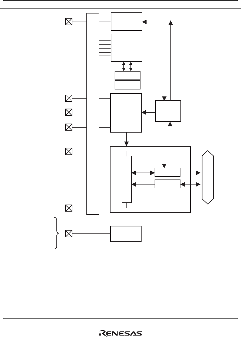
30. User Debugging Interface (H-UDI)
Rev.1.00 Jan. 10, 2008 Page 1488 of 1658
REJ09B0261-0100
TDO
TDI
TRST
TMS
TCK
SDIR
ASEBRK/BRKACK
Boundary-
scan
TAP
controller
Break
controller
TAP
controller
Decoder
SDBSR
SDBPR
SDINT
AUDSYNC
AUDCK
AUDATA3
AUDATA2
AUDATA1
AUDATA0
Trace
controller
Pin multiplexer
Peripheral bus
Shift register
Interrupt/reset
Figure 30.1 Block Diagram of H-UDI

30. User Debugging Interface (H-UDI)
Rev.1.00 Jan. 10, 2008 Page 1489 of 1658
REJ09B0261-0100
30.2 Input/Output Pins
Table 30.1 shows the pin configuration of the H-UDI.
Table 30.1 Pin Configuration of H-UDI
Pin Name Function I/O Description
When Not
in Use
TCK Clock Input
The functions are the same as the serial clock
input pin of JTAG. In synchronization with this
signal, data is sent from the TDI pin to the H-
UDI circuit or data is read from the TDO pin.
Open*1
TMS Mode Input
Mode Select Input Pin
The meaning of data input from the TDI pin is
determined by changing this signal in
synchronization with TCK. The protocol
supports JTAG (IEEE 1149.1) with the subset.
Open*1
TRST*2 Reset Input
H-UDI Reset Input Pin
This signal is received without relating to TCK.
The JTAG interface circuit is reset when this
signal is at a low level. Regardless of whether
JTAG is used or not, TRST should be set to a
low level during a specific period when power is
turned on. This does not conform to the IEEE
standard.
Fixed to
ground or
connected to
the PRESET
pin*3
TDI Data input Input
Data Input Pin
Data is sent to the H-UDI circuit by changing
this signal in synchronization with TCK.
Open*1
TDO Data output Output
Data Output Pin
Data is read from the H-UDI circuit by reading
this signal in synchronization with TCK.
Open
ASEBRK/
BRKACK
Emulator I/O Pins for emulators Open*1
AUDSYNC,
AUDCK,
AUDATA3 to
AUDATA0
Emulator Output
Pins for emulators Open
MPMD Chip-mode Input
Indicates whether the operating mode of this
LSI is emulation support mode (MPMD = 0) or
chip mode (MPMD = 1).
Open

30. User Debugging Interface (H-UDI)
Rev.1.00 Jan. 10, 2008 Page 1490 of 1658
REJ09B0261-0100
Notes: 1. This pin is pulled up in the chip. In designing the board that can connect an emulator, or
using interrupts or resets through the H-UDI, there is no problem with putting the pull-up
resistor outside this LSI.
2. In designing the board that can connect an emulator, or using interrupts or resets
through the H-UDI, the TRST pin should be set so that it can be held low while the
PRESET signal is low after power is turned on and the TRST pin can be controlled
independently.
3. This pin should be connected to ground, or connected to the same signal as the
PRESET, or a pin which operates in the same way as the PRESET pin. When this pin
is connected to ground, the following problem occurs. Since the TRST pin is pulled up
within this LSI, weak current runs when the pin is connected to ground outside the LSI.
The current depends on a resistance of the pull-up for the port pin. Although this current
does not affect the operation of this LSI, it consumes unnecessary power.
The TCK clock or the CPG of this LSI should be set so that the frequency of the TCK clock is less
than that of the peripheral clock of this LSI. For details of the setting of the CPG, see section 15,
Clock Pulse Generator (CPG).

30. User Debugging Interface (H-UDI)
Rev.1.00 Jan. 10, 2008 Page 1491 of 1658
REJ09B0261-0100
30.3 Register Description
The H-UDI has the following registers.
Table 30.2 Register Configuration (1)
CPU Side
Register Name Abbreviation R/W Area P4 Address Area 7 Address Size
Sync
Clock
Instruction register SDIR R H'FC11 0000 H'1C11 0000 16 Pck
Interrupt source register SDINT R/W H'FC11 0018 H'1C11 0018 16 Pck
Boundary scan register SDBSR ⎯ ⎯ ⎯ ⎯ ⎯
Bypass register SDBPR ⎯ ⎯ ⎯ ⎯ ⎯
Table 30.3 Register Configuration (2)
H-UDI Side
Register Name Abbreviation R/W Size Sync Clock
Instruction register SDIR R/W*1 32 Pck
Interrupt source register SDINT W*2 32 Pck
Boundary scan register SDBSR R/W ⎯ ⎯
Bypass register SDBPR R/W 1 ⎯
Notes: 1. The read value from the H-UDI is always fixed to H’FFFF FFFD.
2. 1 can be written to the LSB by the H-UDI interrupt command.
Table 30.4 Register States in Each Processing State
Register Name Abbreviation
Power-On
Reset
Manual
Reset
Module
Standby Sleep
Deep
Sleep
Instruction register SDIR H'0EFF Retained Retained Retained Retained
Interrupt source
register
SDINT H'0000 Retained Retained Retained Retained
30. User Debugging Interface (H-UDI)
Rev.1.00 Jan. 10, 2008 Page 1492 of 1658
REJ09B0261-0100
30.3.1 Instruction Register (SDIR)
SDIR is a 16-bit read-only register that can be read from the CPU. Commands are set via the serial
input pin (TDI). SDIR is initialized by TRST or in the Test-Logic-Reset state of the TAP. This
register can be written to by the H-UDI, regardless of the CPU mode. Operation is not guaranteed
when a reserved command is set to this register.
TI
Bit:
Initial value:
R/W:
15 14 13 12 11 10 9 8 7 6 5 4 3 2 1 0
00 00111011111111
RRRRRRRRRRRRRRRR
Bit Bit Name Initial Value R/W Description
15 to 8 TI 0000 1110 R Test Instruction Bits 7 to 0
0110 xxxx: H-UDI reset negate
0111 xxxx: H-UDI reset assert
101x xxxx: H-UDI interrupt
0000 1110: Initial state
Other than above: Setting prohibited
7 to 0 ⎯ All 1 R Reserved
These bits are always read as 1.
30.3.2 Interrupt Source Register (SDINT)
SDINT is a 16-bit register that can be read from or written to by the CPU. If the H-UDI interrupt
command (Update-IR) is set to SDIR, the INTREQ bit is set to 1. When an H-UDI interrupt
command is set in SDIR, SDINT is connected between the TDI and TDO pins, and becomes a 32-
bit readable register. In this case, the upper 16 bits are 0 and the lower 16 bits are values specified
in SDINT.
Only 0 can be written to the INTREQ bit by the CPU. While this bit is set to 1, an interrupt request
continues to be generated. Therefore, clear this bit to 0 in an interrupt handler and read this bit
again to confirm that this bit is cleared. This register is initialized by TRST or in the test-logic-
reset state.
INTREQ
Bit:
Initial value:
R/W:
15 14 13 12 11 10 9 8 7 6 5 4 3 2 1 0
00 00000000000000
RRRRRRRRRRRRRRR
R/W

30. User Debugging Interface (H-UDI)
Rev.1.00 Jan. 10, 2008 Page 1493 of 1658
REJ09B0261-0100
Bit Bit Name
Initial
Value R/W Description
15 to 1 ⎯ All 0 R Reserved
These bits are always read as 0. The write value
should always be 0.
0 INTREQ 0 R/W Interrupt Request
Indicates whether or not an interrupt by an H-UDI
interrupt command has occurred. Clearing this bit to 0
by the CPU cancels an interrupt request. When writing
1 to this bit, the previous value is maintained.
30.3.3 Bypass Register (SDBPR)
SDBPR is a 1-bit register that supports the JTAG bypass mode. When the BYPASS command is
set to the boundary-scan TAP controller, SDBPR is connected between the TDI and TDO pins.
This register cannot be accessed through the CPU. This register is not initialized by a power-on
reset or assertion of TRST, but it is initialized to 0 by the Capture-DR state.
30.3.4 Boundary Scan Register (SDBSR)
SDBSR is a register that supports the JTAG boundary scan mode. SDBSR is a shift register that is
located on the PAD, to control the input/output pins. By using the SAMPLE/PRELOAD and
EXTEST commands, this register can perform the boundary scan test that supports the JTAG
standard (IEEE 1149.1) with the subset. This register cannot be accessed through the CPU,
regardless of chip mode. This register is not initialized by a power-on reset or assertion of TRST.

30. User Debugging Interface (H-UDI)
Rev.1.00 Jan. 10, 2008 Page 1494 of 1658
REJ09B0261-0100
Table 30.5 Boundary Scan Register Configuration
Number Pin Name Type Number Pin Name Type
From TDI 525 DREQ0 Control
550 DRAK2/CE2A Input 524 DREQ0 Output
549 DRAK2/CE2A Control 523 BACK Input
548 DRAK2/CE2A Output 522 BACK Control
547 DACK3/SCK2/MMCDAT/SIOF
SCK1
Input 521 BACK Output
546 DACK3/SCK2/MMCDAT/SIOF
SCK1
Control 520 BREQ Input
545 DACK3/SCK2/MMCDAT/SIOF
SCK1
Output 519 BREQ Control
544 DACK2/TXD2/MMCCMD/SIOF
TXD1
Input 518 BREQ Output
543 DACK2/TXD2/MMCCMD/SIOF
TXD1
Control 517 STATUS1/DRAK1 Input
542 DACK2/TXD2/MMCCMD/SIOF
TXD1
Output 516 STATUS1/DRAK1 Control
541 DACK1 Input 515 STATUS1/DRAK1 Output
540 DACK1 Control 514 STATUS0/DRAK0 Input
539 DACK1 Output 513 STATUS0/DRAK0 Control
538 DACK0 Input 512 STATUS0/DRAK0 Output
537 DACK0 Control 511 IRL3 Input
536 DACK0 Output 510 IRL3 Control
535 DREQ3/INTC Input 509 IRL3 Output
534 DREQ3/INTC Control 508 IRL2 Input
533 DREQ3/INTC Output 507 IRL2 Control
532 DREQ2/INTB Input 506 IRL2 Output
531 DREQ2/INTB Control 505 IRL1 Input
530 DREQ2/INTB Output 504 IRL1 Control
529 DREQ1 Input 503 IRL1 Output
528 DREQ1 Control 502 IRL0 Input
527 DREQ1 Output 501 IRL0 Control
526 DREQ0 Input 500 IRL0 Output

30. User Debugging Interface (H-UDI)
Rev.1.00 Jan. 10, 2008 Page 1495 of 1658
REJ09B0261-0100
Number Pin Name Type Number Pin Name Type
499 NMI Input
467 REQ0/REQOUT Control
498 NMI Control
466 REQ0/REQOUT Output
497 NMI Output
465 PERR Input
496 INTA Input
464 PERR Control
495 INTA Control
463 PERR Output
494 INTA Output
462 SERR Input
493 CLK/DCLKIN Input
461 SERR Control
492 PCIRESET Input
460 SERR Output
491 PCIRESET Control
459 STOP/CDE Input
490 PCIRESET Output
458 STOP/CDE Control
489 GNT3/MMCCLK Input
457 STOP/CDE Output
488 GNT3/MMCCLK Control
456 PAR Input
487 GNT3/MMCCLK Output
455 PAR Control
486 GNT2 Input
454 PAR Output
485 GNT2 Control
453 DEVSEL/DCLKOUT Input
484 GNT2 Output
452 DEVSEL/DCLKOUT Control
483 GNT1 Input
451 DEVSEL/DCLKOUT Output
482 GNT1 Control
450 LOCK/ODDF Input
481 GNT1 Output
449 LOCK/ODDF Control
480 REQ3/MMCCD Input
448 LOCK/ODDF Output
479 REQ3/MMCCD Control
447 IDSEL Input
478 REQ3/MMCCD Output
446 IDSEL Control
477 REQ2 Input
445 IDSEL Output
476 REQ2 Control
444 TRDY/DISP Input
475 REQ2 Output
443 TRDY/DISP Control
474 REQ1 Input
442 TRDY/DISP Output
473 REQ1 Control
441 IRDY/HSYNC Input
472 REQ1 Output
440 IRDY/HSYNC Control
471 GNT0/GNTIN Input
439 IRDY/HSYNC Output
470 GNT0/GNTIN Control
438 FRAME/VSYNC Input
469 GNT0/GNTIN Output
437 FRAME/VSYNC Control
468 REQ0/REQOUT Input
436 FRAME/VSYNC Output

30. User Debugging Interface (H-UDI)
Rev.1.00 Jan. 10, 2008 Page 1496 of 1658
REJ09B0261-0100
Number Pin Name Type Number Pin Name Type
435 WE7/CBE3 Input
403 D57/AD25 Output
434 WE7/CBE3 Control
402 D56/AD24 Input
433 WE7/CBE3 Output
401 D56/AD24 Control
432 WE6/CBE2 Input
400 D56/AD24 Output
431 WE6/CBE2 Control
399 D55/AD23 Input
430 WE6/CBE2 Output
398 D55/AD23 Control
429 WE5/CBE1 Input
397 D55/AD23 Output
428 WE5/CBE1 Control
396 D54/AD22 Input
427 WE5/CBE1 Output
395 D54/AD22 Control
426 WE4/CBE0 Input
394 D54/AD22 Output
425 WE4/CBE0 Control
393 D53/AD21 Input
424 WE4/CBE0 Output
392 D53/AD21 Control
423 D63/AD31 Input
391 D53/AD21 Output
422 D63/AD31 Control
390 D52/AD20 Input
421 D63/AD31 Output
389 D52/AD20 Control
420 D62/AD30 Input
388 D52/AD20 Output
419 D62/AD30 Control
387 D51/AD19 Input
418 D62/AD30 Output
386 D51/AD19 Control
417 D61/AD29 Input
385 D51/AD19 Output
416 D61/AD29 Control
384 D50/AD18 Input
415 D61/AD29 Output
383 D50/AD18 Control
414 D60/AD28 Input
382 D50/AD18 Output
413 D60/AD28 Control
381 D49/AD17/DB5 Input
412 D60/AD28 Output
380 D49/AD17/DB5 Control
411 D59/AD27 Input
379 D49/AD17/DB5 Output
410 D59/AD27 Control
378 D48/AD16/DB4 Input
409 D59/AD27 Output
377 D48/AD16/DB4 Control
408 D58/AD26 Input
376 D48/AD16/DB4 Output
407 D58/AD26 Control
375 D47/AD15/DB3 Input
406 D58/AD26 Output
374 D47/AD15/DB3 Control
405 D57/AD25 Input
373 D47/AD15/DB3 Output
404 D57/AD25 Control
372 D46/AD14/DB2 Input

30. User Debugging Interface (H-UDI)
Rev.1.00 Jan. 10, 2008 Page 1497 of 1658
REJ09B0261-0100
Number Pin Name Type Number Pin Name Type
371 D46/AD14/DB2 Control
340 D36/AD4/DR4 Output
370 D46/AD14/DB2 Output
339 D35/AD3/DR3 Input
369 D45/AD13/DB1 Input
338 D35/AD3/DR3 Control
368 D45/AD13/DB1 Control
337 D35/AD3/DR3 Output
367 D45/AD13/DB1 Output
336 D34/AD2/DR2 Input
366 D44/AD12/DB0 Input
335 D34/AD2/DR2 Control
365 D44/AD12/DB0 Control
334 D34/AD2/DR2 Output
364 D44/AD12/DB0 Output
333 D33/AD1/DR1 Input
363 D43/AD11/DG5 Input
332 D33/AD1/DR1 Control
362 D43/AD11/DG5 Control
331 D33/AD1/DR1 Output
361 D43/AD11/DG5 Output
330 D32/AD0/DR0 Input
360 D42/AD10/DG4 Input
329 D32/AD0/DR0 Control
359 D42/AD10/DG4 Control
328 D32/AD0/DR0 Output
358 D42/AD10/DG4 Output
327 CLKOUTENB Input
357 D41/AD9/DG3 Input
326 CLKOUTENB Control
356 D41/AD9/DG3 Control
325 CLKOUTENB Output
355 D41/AD9/DG3 Output
324 CLKOUT Input
354 D40/AD8/DG2 Input
323 CLKOUT Control
353 D40/AD8/DG2 Control
322 CLKOUT Output
352 D40/AD8/DG2 Output
321 RDY Input
351 D39/AD7/DG1 Input
320 RDY Control
350 D39/AD7/DG1 Control
319 RDY Output
349 D39/AD7/DG1 Output
318 WE3 Input
348 D38/AD6/DG0 Input
317 WE3 Control
347 D38/AD6/DG0 Control
316 WE3 Output
346 D38/AD6/DG0 Output
315 WE2 Input
345 D37/AD5/DR5 Input
314 WE2 Control
344 D37/AD5/DR5 Control
313 WE2 Output
343 D37/AD5/DR5 Output
312 WE1 Input
342 D36/AD4/DR4 Input
311 WE1 Control
341 D36/AD4/DR4 Control
310 WE1 Output

30. User Debugging Interface (H-UDI)
Rev.1.00 Jan. 10, 2008 Page 1498 of 1658
REJ09B0261-0100
Number Pin Name Type Number Pin Name Type
309 WE0 Input
277 CS0 Output
308 WE0 Control
276 A25 Input
307 WE0 Output
275 A25 Control
306 BS Input
274 A25 Output
305 BS Control
273 A24 Input
304 BS Output
272 A24 Control
303 R/W Input
271 A24 Output
302 R/W Control
270 A23 Input
301 R/W Output
269 A23 Control
300 RD Input
268 A23 Output
299 RD Control
267 A22 Input
298 RD Output
266 A22 Control
297 CS6 Input
265 A22 Output
296 CS6 Control
264 A21 Input
295 CS6 Output
263 A21 Control
294 CS5 Input
262 A21 Output
293 CS5 Control
261 A20 Input
292 CS5 Output
260 A20 Control
291 CS4 Input
259 A20 Output
290 CS4 Control
258 A19 Input
289 CS4 Output
257 A19 Control
288 CS3 Input
256 A19 Output
287 CS3 Control
255 A18 Input
286 CS3 Output
254 A18 Control
285 CS2 Input
253 A18 Output
284 CS2 Control
252 A17 Input
283 CS2 Output
251 A17 Control
282 CS1 Input
250 A17 Output
281 CS1 Control
249 A16 Input
280 CS1 Output
248 A16 Control
279 CS0 Input
247 A16 Output
278 CS0 Control
246 A15 Input

30. User Debugging Interface (H-UDI)
Rev.1.00 Jan. 10, 2008 Page 1499 of 1658
REJ09B0261-0100
Number Pin Name Type Number Pin Name Type
245 A15 Control
213 A4 Input
244 A15 Output
212 A4 Control
243 A14 Input
211 A4 Output
242 A14 Control
210 A3 Input
241 A14 Output
209 A3 Control
240 A13 Input
208 A3 Output
239 A13 Control
207 A2 Input
238 A13 Output
206 A2 Control
237 A12 Input
205 A2 Output
236 A12 Control
204 A1 Input
235 A12 Output
203 A1 Control
234 A11 Input
202 A1 Output
233 A11 Control
201 A0 Input
232 A11 Output
200 A0 Control
231 A10 Input
199 A0 Output
230 A10 Control
198 D31 Input
229 A10 Output
197 D31 Control
228 A9 Input
196 D31 Output
227 A9 Control
195 D30 Input
226 A9 Output
194 D30 Control
225 A8 Input
193 D30 Output
224 A8 Control
192 D29 Input
223 A8 Output
191 D29 Control
222 A7 Input
190 D29 Output
221 A7 Control
189 D28 Input
220 A7 Output
188 D28 Control
219 A6 Input
187 D28 Output
218 A6 Control
186 D27 Input
217 A6 Output
185 D27 Control
216 A5 Input
184 D27 Output
215 A5 Control
183 D26 Input
214 A5 Output
182 D26 Control

30. User Debugging Interface (H-UDI)
Rev.1.00 Jan. 10, 2008 Page 1500 of 1658
REJ09B0261-0100
Number Pin Name Type Number Pin Name Type
181 D26 Output
149 D15 Control
180 D25 Input
148 D15 Output
179 D25 Control
147 D14 Input
178 D25 Output
146 D14 Control
177 D24 Input
145 D14 Output
176 D24 Control
144 D13 Input
175 D24 Output
143 D13 Control
174 D23 Input
142 D13 Output
173 D23 Control
141 D12 Input
172 D23 Output
140 D12 Control
171 D22 Input
139 D12 Output
170 D22 Control
138 D11 Input
169 D22 Output
137 D11 Control
168 D21 Input
136 D11 Output
167 D21 Control
135 D10 Input
166 D21 Output
134 D10 Control
165 D20 Input
133 D10 Output
164 D20 Control
132 D9 Input
163 D20 Output
131 D9 Control
162 D19 Input
130 D9 Output
161 D19 Control
129 D8 Input
160 D19 Output
128 D8 Control
159 D18 Input
127 D8 Output
158 D18 Control
126 D7 Input
157 D18 Output
125 D7 Control
156 D17 Input
124 D7 Output
155 D17 Control
123 D6 Input
154 D17 Output
122 D6 Control
153 D16 Input
121 D6 Output
152 D16 Control
120 D5 Input
151 D16 Output
119 D5 Control
150 D15 Input
118 D5 Output

30. User Debugging Interface (H-UDI)
Rev.1.00 Jan. 10, 2008 Page 1501 of 1658
REJ09B0261-0100
Number Pin Name Type Number Pin Name Type
117 D4 Input
86 MODE9/TXD4/FD1 Input
116 D4 Control
85 MODE9/TXD4/FD1 Control
115 D4 Output
84 MODE9/TXD4/FD1 Output
114 D3 Input
83 MODE8/SCK3/FD0 Input
113 D3 Control
82 MODE8/SCK3/FD0 Control
112 D3 Output
81 MODE8/SCK3/FD0 Output
111 D2 Input
80 MODE7/RXD3/FALE Input
110 D2 Control
79 MODE7/RXD3/FALE Control
109 D2 Output
78 MODE7/RXD3/FALE Output
108 D1 Input
77 MODE6/SIOFSYNC1 Input
107 D1 Control
76 MODE6/SIOFSYNC1 Control
106 D1 Output
75 MODE6/SIOFSYNC1 Output
105 D0 Input
74 MODE5/SIOFMCLK1 Input
104 D0 Control
73 MODE5/SIOFMCLK1 Control
103 D0 Output
72 MODE5/SIOFMCLK1 Output
102 MRESETOUT/IRQOUT Input
71 MODE4/TXD3/FCLE Input
101 MRESETOUT/IRQOUT Control
70 MODE4/TXD3/FCLE Control
100 MRESETOUT/IRQOUT Output
69 MODE4/TXD3/FCLE Output
99 MODE14 Input
68 MODE3/IRL7/FD7 Input
98 MODE13/TCLK/IOIS16 Input
67 MODE3/IRL7/FD7 Control
97 MODE13/TCLK/IOIS16 Control
66 MODE3/IRL7/FD7 Output
96 MODE13/TCLK/IOIS16 Output
65 MODE2/IRL6/FD6 Input
95 MODE12/DRAK3/CE2B Input
64 MODE2/IRL6/FD6 Control
94 MODE12/DRAK3/CE2B Control
63 MODE2/IRL6/FD6 Output
93 MODE12/DRAK3/CE2B Output
62 MODE1/IRL5/FD5 Input
92 MODE11/SCK4/FD3 Input
61 MODE1/IRL5/FD5 Control
91 MODE11/SCK4/FD3 Control
60 MODE1/IRL5/FD5 Output
90 MODE11/SCK4/FD3 Output
59 MODE0/IRL4/FD4 Input
89 MODE10/RXD4/FD2 Input
58 MODE0/IRL4/FD4 Control
88 MODE10/RXD4/FD2 Control
57 MODE0/IRL4/FD4 Output
87 MODE10/RXD4/FD2 Output
56 SCK5/HAC1/SDOUT/SSI1/
SDATA
Input

30. User Debugging Interface (H-UDI)
Rev.1.00 Jan. 10, 2008 Page 1502 of 1658
REJ09B0261-0100
Number Pin Name Type Number Pin Name Type
55 SCK5/HAC1/SDOUT/SSI1/
SDATA
Control 26 SCK1 Input
54 SCK5/HAC1/SDOUT/SSI1/
SDATA
Output 25 SCK1 Control
53 RXD5/HAC1/SDIN/SSI1/SCK Input
24 SCK1 Output
52 RXD5/HAC1/SDIN/SSI1/SCK Control
23 RXD1 Input
51 RXD5/HAC1/SDIN/SSI1/SCK Output
22 RXD1 Control
50 TXD5/HAC1/SYNC/SSI1/WS Input
21 RXD1 Output
49 TXD5/HAC1/SYNC/SSI1/WS Control
20 TXD1 Input
48 TXD5/HAC1/SYNC/SSI1/WS Output
19 TXD1 Control
47 HAC1/BITCLK/SSI1/CLK Input
18 TXD1 Output
46 HAC1/BITCLK/SSI1/CLK Control
17 CTS0/INTD/FCE Input
45 HAC1/BITCLK/SSI1/CLK Output
16 CTS0/INTD/FCE Control
44 TXD/HAC0/SDOUT/SSI0/SDATA Input
15 CTS0/INTD/FCE Output
43 TXD/HAC0/SDOUT/SSI0/SDATA Control
14 RTS0/HSPI/CS/FSE Input
42 TXD/HAC0/SDOUT/SSI0/SDATA Output
13 RTS0/HSPI/CS/FSE Control
41 RXD/HAC0/SDIN/SSI0/SCK Input
12 RTS0/HSPI/CS/FSE Output
40 RXD/HAC0/SDIN/SSI0/SCK Control
11 SCK0/HSPI/CLK/FRE Input
39 RXD/HAC0/SDIN/SSI0/SCK Output
10 SCK0/HSPI/CLK/FRE Control
38 SYNC/HAC0/SYNC/SSI0/WS Input
9 SCK0/HSPI/CLK/FRE Output
37 SYNC/HAC0/SYNC/SSI0/WS Control
8 RXD0/HSPI/RX/FR/B Input
36 SYNC/HAC0/SYNC/SSI0/WS Output
7 RXD0/HSPI/RX/FR/B Control
35 MCLK/HAC/RES Input
6 RXD0/HSPI/RX/FR/B Output
34 MCLK/HAC/RES Control
5 TXD0/HSPI/TX/FWE Input
33 MCLK/HAC/RES Output
4 TXD0/HSPI/TX/FWE Control
32 SCK/HAC0/BITCLK/SSI0/CLK Input
3 TXD0/HSPI/TX/FWE Output
31 SCK/HAC0/BITCLK/SSI0/CLK Control
2 ASEBRK Input
30 SCK/HAC0/BITCLK/SSI0/CLK Output
1 ASEBRK Control
29 RXD2/SIOFRXD1 Input
0 ASEBRK Output
28 RXD2/SIOFRXD1 Control
To TDO
27 RXD2/SIOFRXD1 Output
Note: * Control means a low-active signal. When a low-active signal is driven low, the
corresponding pin is driven by the output value.

30. User Debugging Interface (H-UDI)
Rev.1.00 Jan. 10, 2008 Page 1503 of 1658
REJ09B0261-0100
30.4 Operation
30.4.1 Boundary-Scan TAP Controller (IDCODE, EXTEST, SAMPLE/PRELOAD, and
BYPASS)
In the H-UDI in this LSI, the boundary-scan TAP controller is separated from the TAP controller
for other H-UDI function control. When the TRST is asserted (including when the power is turned
on), the boundary-scan TAP controller operates and the boundary scan function specified in JTAG
can be used. By inputting the switching command, an H-UDI reset and H-UDI interrupts can be
used. However, the following restrictions are put on this LSI.
• Clock-related pins (EXTAL and XTAL) are out of the scope of the boundary scan test.
• Reset-related pin (PRESET) is out of the scope of the boundary scan test.
• H-UDI-related pins (TCK, TDI, TDO, TMS, TRST, AUDSYNC, AUDCK, AUDATA3 to
AUDATA0, and MPMD) are out of the scope of the boundary scan test.
• DDRIF-related pins are out of the scope of the boundary scan test.
• During the boundary scan (IDCODE, EXTEST, SAMPLE/PRELOAD, BYPASS, and H-UDI
switching command), the maximum frequency of TCK is 10 MHz.
• The access size from the H-UDI to the boundary-scan TAP controller is 8 bits.
The commands supported by the boundary-scan TAP controller are shown below.
Note: During the boundary scan, the MPMD and the PRESET pins should be fixed to high level.
When the H-UDI operates in emulation support mode (MPMD = 0), the boundary scan
function cannot be used. Figure 30.2 shows the sequence to switch from the boundary-
scan TAP controller to the H-UDI.
Table 30.6 Commands Supported by Boundary-Scan TAP Controller
Bit 7 Bit 6 Bit 5 Bit 4 Bit 3 Bit 2 Bit 1 Bit 0 Description
0 1 0 1 0 1 0 1 IDCODE
1 1 1 1 1 1 1 1 BYPASS
0 0 0 0 0 0 0 0 EXTEST
0 1 0 0 0 0 0 0 SAMPLE/PRELOAD
0 0 0 0 1 0 0 0 H-UDI switching command
Other than above Setting prohibited
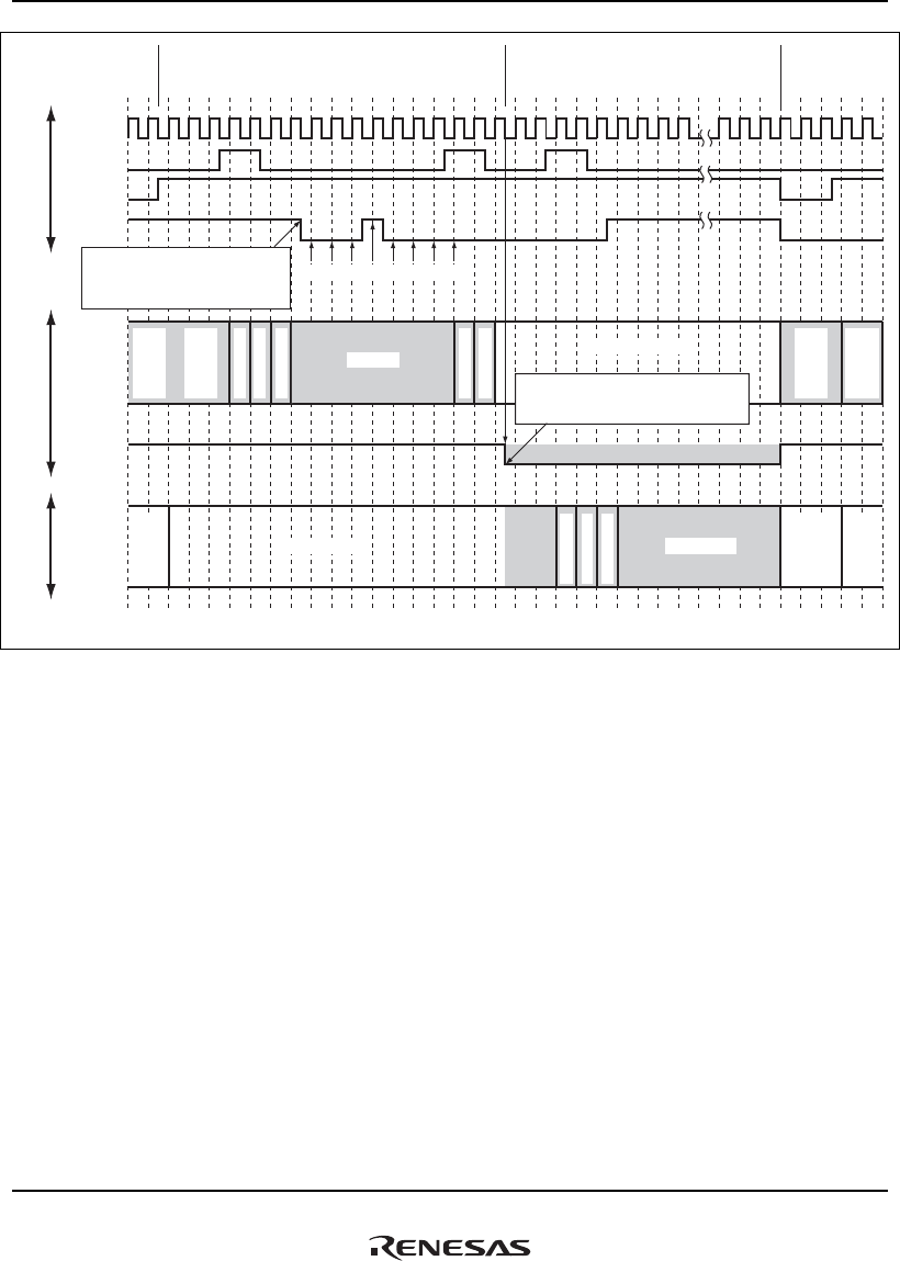
30. User Debugging Interface (H-UDI)
Rev.1.00 Jan. 10, 2008 Page 1504 of 1658
REJ09B0261-0100
00010000
Test-Logic
-Reset
Run-Test
-Idle
Run-Test-Idle
Test-Logic
-Reset
Shift-IR
Test-Logic
-Reset
Run-Test
-Idle
Test-Logic
-Reset
Run-Test
-Idle
Shift-IR
TCK
TMS
TRST
TDI
H-UDI
Run-Test-Idle
TRST is
asserted
H-UDI switching command is input to
boundary-scan TAP controller H-UDI is used
TRST is
asserted
Boundary-scan TAP
controller External pins
H-UDI
selection
Status
Note: The hatched sections represent the functions connected to the external pins.
Status
H-UDI switching command (B'00001000)
(when Shift-IR state > 8 cycles,
input of last 8 cycles is valid)
Switchover is determined at falling of
first tck cycle after the boundary-scan TAP
controller has entered the Run-Test/Idle state
Select-DR
Select-IR
Capture-IR
Exit1-IR
Update-IR
Select-DR
Select-IR
Capture-IR
Figure 30.2 Sequence to Switch from Boundary-Scan TAP Controller to H-UDI
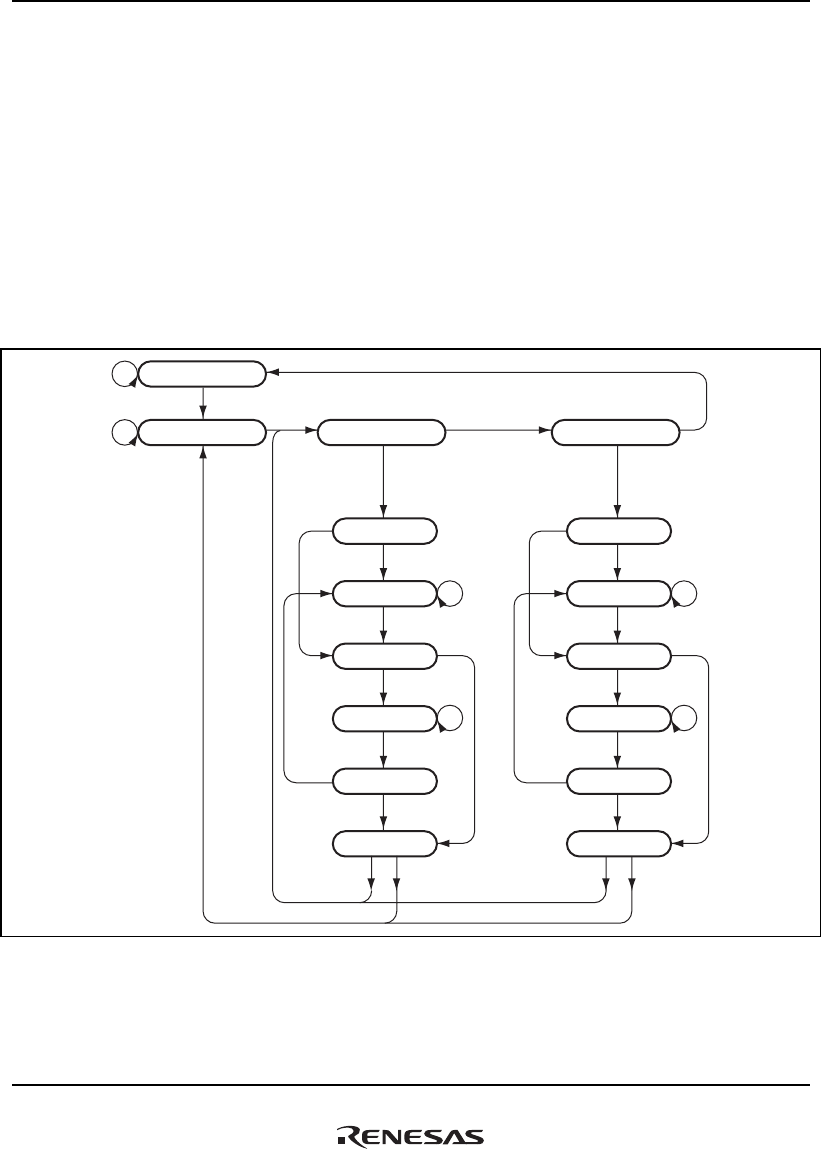
30. User Debugging Interface (H-UDI)
Rev.1.00 Jan. 10, 2008 Page 1505 of 1658
REJ09B0261-0100
30.4.2 TAP Control
Figure 30.3 shows the internal states of the TAP controller. The controller supports the state
transitions specified in JTAG with the subset.
• The condition of transition is the TMS value at the rising edge of TCK.
• The TDI value is sampled at the rising edge of TCK and shifted at the falling edge of TCK.
• The TDO value is changed at the falling edge of TCK. The TDO is in the high impedance state
other than in the Shift-DR or Shift-IR state.
• When TRST is changed to 0, the transition to the Test-Logic-Reset state is performed
asynchronously with the TCK signal.
Test -Logic-Reset
Capture-DR
Shift-DR
Exit1-DR
Pause-DR
Exit2-DR
Update-DR
Select-DR-ScanRun-Test/Idle
1
0
0
0
0
11 1
1
0
0
0
1
11
0
1
1
10
Capture-IR
Shift-IR
Exit1-IR
Pause-IR
Exit2-IR
Update-IR
Select-IR-Scan
0
0
1
0
0
0
1
0
1
1
10
Figure 30.3 Diagram of Transitions of TAP Controller State
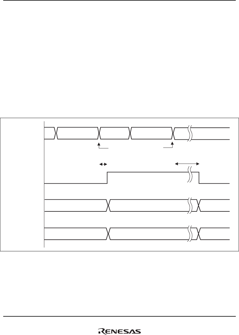
30. User Debugging Interface (H-UDI)
Rev.1.00 Jan. 10, 2008 Page 1506 of 1658
REJ09B0261-0100
30.4.3 H-UDI Reset
The H-UDI is reset by a power-on reset by the SDIR command. To reset the H-UDI, send the H-
UDI reset assert command from the H-UDI pin, and then send the H-UDI reset negate command
(see figure 30.4). The time required between the H-UDI reset assert and H-UDI reset negate
commands is the same as the time to keep the reset pin low in order to reset this LSI by a power-
on reset. After the H-UDI reset assert command is set, the reset signal is asserted in the chip after
four cycles at a peripheral clock (Pck). When the H-UDI reset negate command is set, the reset
signal is negated in the chip after a reset hold period. (The minimum period is 17 cycles at a
peripheral clock, and the maximum period is 42 cycles at a peripheral clock. For details, see
section 15, Clock Pulse Generator (CPG).)
Note: The WDT/RST module is not initialized. However, the overflow counter of the WDT/RST
module is initialized.
Reset in the chip
H-UDI
reset asserted
H-UDI
reset negated
H-UDI pin
Command set timing
Pck 4 cycles Reset hold period
Reset
Normal Reset processing
CPU state
STATUS[1:0] output LL (normal) HH (reset) LL (normal)
Figure 30.4 H-UDI Reset

30. User Debugging Interface (H-UDI)
Rev.1.00 Jan. 10, 2008 Page 1507 of 1658
REJ09B0261-0100
30.4.4 H-UDI Interrupt
The H-UDI interrupt function generates an interrupt by setting a command value in SDIR through
the H-UDI. The H-UDI interrupt function is general exception or interrupt operation, that is,
execution is branched to the address based on VBR and is returned to the branch source by the
RTE instruction. In this case, the exception code stored in INTEVT is H'600. Also, the priority of
the H-UDI interrupt is controlled by bits 28 to 24 in INT2PRI4. For details, see section 10,
Interrupt Controller (INTC).
An H-UDI interrupt request signal is asserted when the INTREQ bit in SDINT is set to 1 after
setting the command (Update-IRQ). Since the interrupt request signal is not negated unless the
INTREQ bit is cleared to 0 by software, the interrupt request cannot be missed. While the H-UDI
interrupt command is set in SDIR, SDINT is connected between the TDI and TDO pins. For
values read through the TDO pin and others, see section 30.3.2, Interrupt Source Register
(SDINT).
30.5 Usage Notes
1. Once the SDIR command is set, it is not changed unless a command is written through the H-
UDI, except the assertion of TRST or initialization by changing the TAP to the Test-Logic-
Reset state.
2. Sleep mode and deep sleep mode are released by an H-UDI interrupt or H-UDI reset, and these
modes accept the interrupt and reset requests.
3. The H-UDI is used to connect an emulator. Therefore, the JTAG functions cannot be used
when an emulator is used.

30. User Debugging Interface (H-UDI)
Rev.1.00 Jan. 10, 2008 Page 1508 of 1658
REJ09B0261-0100

31. Register List
Rev.1.00 Jan. 10, 2008 Page 1509 of 1658
REJ09B0261-0100
Section 31 Register List
This section is a summary of the contents of the descriptions of on-chip I/O registers in the
individual sections.
31.1 Register Address List
The addresses of the I/O registers incorporated in the SH7785 are listed in table 31.1. The registers
are grouped by functional module, and these appear in the same order as the sections of the
manual. Since this is a summary, parts of the descriptions, along with the notes, have been
omitted. For details on the registers, refer to the descriptions in the corresponding sections.
Notes: 1. Access to undefined and reserved addresses is prohibited.
2. Access in an access unit other than that specified in this list is prohibited.
3. The register addresses are given as the P4-area address (the P4 area of the virtual
address space) and the area-7 address (accessed in area 7 of the physical address space
by using the TLB).
4. In the case of the PCIC module, entries under "R/W" indicate the state of the
SuperHyway bus in which the given register is accessed.

31. Register List
Rev.1.00 Jan. 10, 2008 Page 1510 of 1658
REJ09B0261-0100
Table 31.1 Register Address List
Module
Name Name Abbreviation R/W
P4 Area
Address
Area 7
Address
Access
Size
TRAPA exception register TRA R/W H'FF00 0020 H'1F00 0020 32
Exception
processing Exception event register EXPEVT R/W H'FF00 0024 H'1F00 0024 32
Interrupt event register INTEVT R/W H'FF00 0028 H'1F00 0028 32
Non-support detection exception register EXPMASK R/W H'FF2F 0004 H'1F2F 0004 32
MMU Page table entry high register PTEH R/W H'FF00 0000 H'1F00 0000 32
Page table entry low register PTEL R/W H'FF00 0004 H'1F00 0004 32
Translation table base register TTB R/W H'FF00 0008 H'1F00 0008 32
TLB exception address register TEA R/W H'FF00 000C H'1F00 000C 32
MMU control register MMUCR R/W H'FF00 0010 H'1F00 0010 32
Physical address space control register PASCR R/W H'FF00 0070 H'1F00 0070 32
Instruction re-fetch inhibit control register IRMCR R/W H'FF00 0078 H'1F00 0078 32
Page table entry assistance register PTEA R/W H'FF00 0034 H'1F00 0034 32
Cache Cache control register CCR R/W H'FF00 001C H'1F00 001C 32
Queue address control register 0 QACR0 R/W H'FF00 0038 H'1F00 0038 32
Queue address control register 1 QACR1 R/W H'FF00 003C H'1F00 003C 32
On-chip memory control register RAMCR R/W H'FF00 0074 H'1F00 0074 32
L memory L memory transfer source address register 0 LSA0 R/W H'FF000050 H'1F000050 32
L memory transfer source address register 1 LSA1 R/W H'FF000054 H'1F000054 32
L memory transfer destination address
register 0
LDA0 R/W H'FF000058 H'1F000058 32
L memory transfer destination address
register 1
LDA1 R/W H'FF00005C H'1F00005C 32
INTC Interrupt control register 0 ICR0 R/W H'FFD0 0000 H'1FD0 0000 32
Interrupt control register 1 ICR1 R/W H'FFD0 001C H'1FD0 001C 32
Interrupt priority register INTPRI R/W H'FFD0 0010 H'1FD0 0010 32
Interrupt source register INTREQ R/(W)*1 H'FFD0 0024 H'1FD0 0024 32
Interrupt mask register 0 INTMSK0 R/W H'FFD0 0044 H'1FD0 0044 32
Interrupt mask register 1 INTMSK1 R/W H'FFD0 0048 H'1FD0 0048 32
Interrupt mask register 2 INTMSK2 R/W H'FFD4 0080 H'1FD4 0080 32
Interrupt mask clear register 0 INTMSKCLR0 R/W H'FFD0 0064 H'1FD0 0064 32

31. Register List
Rev.1.00 Jan. 10, 2008 Page 1511 of 1658
REJ09B0261-0100
Module
Name Name Abbreviation R/W
P4 Area
Address
Area 7
Address
Access
Size
INTC Interrupt mask clear register 1 INTMSKCLR1 R/W H'FFD0 0068 H'1FD0 0068 32
Interrupt mask clear register 2 INTMSKCLR2 R/W H'FFD4 0084 H'1FD4 0084 32
NMI flag control register NMIFCR R/(W)*2 H'FFD0 00C0 H'1FD0 00C0 32
User interrupt mask level register USERIMASK R/W H'FFD3 0000 H'1FD3 0000 32
Interrupt priority register 0 INT2PRI0 R/W H'FFD4 0000 H'1FD4 0000 32
Interrupt priority register 1 INT2PRI1 R/W H'FFD4 0004 H'1FD4 0004 32
Interrupt priority register 2 INT2PRI2 R/W H'FFD4 0008 H'1FD4 0008 32
Interrupt priority register 3 INT2PRI3 R/W H'FFD4 000C H'1FD4 000C 32
Interrupt priority register 4 INT2PRI4 R/W H'FFD4 0010 H'1FD4 0010 32
Interrupt priority register 5 INT2PRI5 R/W H'FFD4 0014 H'1FD4 0014 32
Interrupt priority register 6 INT2PRI6 R/W H'FFD4 0018 H'1FD4 0018 32
Interrupt priority register 7 INT2PRI7 R/W H'FFD4 001C H'1FD4 001C 32
Interrupt priority register 8 INT2PRI8 R/W H'FFD4 0020 H'1FD4 0020 32
Interrupt priority register 9 INT2PRI9 R/W H'FFD4 0024 H'1FD4 0024 32
Interrupt source register
(not affected by the mask state)
INT2A0 R H'FFD4 0030 H'1FD4 0030 32
Interrupt source register
(affected by the mask state)
INT2A1 R H'FFD4 0034 H'1FD4 0034 32
Interrupt mask register INT2MSKR R/W H'FFD4 0038 H'1FD4 0038 32
Interrupt mask clear register INT2MSKCLR R/W H'FFD4 003C H'1FD4 003C 32
On-chip module interrupt source register 0 INT2B0 R H'FFD4 0040 H'1FD4 0040 32
On-chip module interrupt source register 1 INT2B1 R H'FFD4 0044 H'1FD4 0044 32
On-chip module interrupt source register 2 INT2B2 R H'FFD4 0048 H'1FD4 0048 32
On-chip module interrupt source register 3 INT2B3 R H'FFD4 004C H'1FD4 004C 32
On-chip module interrupt source register 4 INT2B4 R H'FFD4 0050 H'1FD4 0050 32
On-chip module interrupt source register 5 INT2B5 R H'FFD4 0054 H'1FD4 0054 32
On-chip module interrupt source register 6 INT2B6 R H'FFD4 0058 H'1FD4 0058 32
On-chip module interrupt source register 7 INT2B7 R H'FFD4 005C H'1FD4 005C 32
GPIO interrupt set register INT2GPIC R/W H'FFD4 0090 H'1FD4 0090 32
LBSC Memory Address Map Select Register MMSELR R/W H'FF40 0020 H'1F40 0020 32
Bus Control Register BCR R/W H'FF80 1000 H'1F80 1000 32
CS0 Bus Control Register CS0BCR R/W H'FF80 2000 H'1F80 2000 32

31. Register List
Rev.1.00 Jan. 10, 2008 Page 1512 of 1658
REJ09B0261-0100
Module
Name Name Abbreviation R/W
P4 Area
Address
Area 7
Address
Access
Size
LBSC CS1 Bus Control Register CS1BCR R/W H'FF80 2010 H'1F80 2010 32
CS2 Bus Control Register CS2BCR R/W H'FF80 2020 H'1F80 2020 32
CS3 Bus Control Register CS3BCR R/W H'FF80 2030 H'1F80 2030 32
CS4 Bus Control Register CS4BCR R/W H'FF80 2040 H'1F80 2040 32
CS5 Bus Control Register CS5BCR R/W H'FF80 2050 H'1F80 2050 32
CS6 Bus Control Register CS6BCR R/W H'FF80 2060 H'1F80 2060 32
CS0 Wait Control Register CS0WCR R/W H'FF80 2008 H'1F80 2008 32
CS1 Wait Control Register CS1WCR R/W H'FF80 2018 H'1F80 2018 32
CS2 Wait Control Register CS2WCR R/W H'FF80 2028 H'1F80 2028 32
CS3 Wait Control Register CS3WCR R/W H'FF80 2038 H'1F80 2038 32
CS4 Wait Control Register CS4WCR R/W H'FF80 2048 H'1F80 2048 32
CS5 Wait Control Register CS5WCR R/W H'FF80 2058 H'1F80 2058 32
CS6 Wait Control Register CS6WCR R/W H'FF80 2068 H'1F80 2068 32
CS5 PCMCIA Control Register CS5PCR R/W H'FF80 2070 H'1F80 2070 32
CS6 PCMCIA Control Register CS6PCR R/W H'FF80 2080 H'1F80 2080 32
DDR2IF DBSC2 status register DBSTATE R H'FE80 000C H'1E80 000C 32
SDRAM operation enable register DBEN R/W H'FE80 0010 H'1E80 0010 32
SDRAM command control register DBCMDCNT R/W H'FE80 0014 H'1E80 0014 32
SDRAM configuration setting register DBCONF R/W H'FE80 0020 H'1E80 0020 32
SDRAM timing register 0 DBTR0 R/W H'FE80 0030 H'1E80 0030 32
SDRAM timing register 1 DBTR1 R/W H'FE80 0034 H'1E80 0034 32
SDRAM timing register 2 DBTR2 R/W H'FE80 0038 H'1E80 0038 32
SDRAM refresh control register 0 DBRFCNT0 R/W H'FE80 0040 H'1E80 0040 32
SDRAM refresh control register 1 DBRFCNT1 R/W H'FE80 0044 H'1E80 0044 32
SDRAM refresh control register 2 DBRFCNT2 R/W H'FE80 0048 H'1E80 0048 32
SDRAM refresh status register DBRFSTS R/W H'FE80 004C H'1E80 004C 32
DDRPAD frequency setting register DBFREQ R/W H'FE80 0050 H'1E80 0050 32
DDRPAD DIC, ODT, OCD setting register DBDICODTOCD R/W H'FE80 0054 H'1E80 0054 32
SDRAM mode setting register DBMRCNT W H'FE80 0060 H'1E80 0060 32

31. Register List
Rev.1.00 Jan. 10, 2008 Page 1513 of 1658
REJ09B0261-0100
Modul e
Name Name Abbreviation R/W
P4 Area
Address
Area 7
Address
Access
Size
PCIC Control register space (physical address: H'FE04 0000 to H'FE04 00FF)
PCIC enable control register PCIECR R/W H'FE00 0008 H'1E00 0008 32
PCI configuration register space (physical address: H'FE04 0000 to H'FE04 00FF)
PCI vendor ID register PCIVID R H'FE04 0000 H'1E04 0000 (32)/16/8
PCI device ID register PCIDID R H'FE04 0002 H'1E04 0002 (32)/16/8
PCI command register PCICMD R/W H'FE04 0004 H'1E04 0004 (32)/16/8
PCI status register PCISTATUS R/W H'FE04 0006 H'1E04 0006 (32)/16/8
PCI revision ID register PCIRID R H'FE04 0008 H'1E04 0008 (32)/(16)/
8
PCI program interface register PCIPIF R/W H'FE04 0009 H'1E04 0009 (32)/(16)/
8
PCI sub class code register PCISUB R/W H'FE04 000A H'1E04 000A (32)/(16)/
8
PCI base class code register PCIBCC R/W H'FE04 000B H'1E04 000B (32)/(16)/
8
PCI cache line size register PCICLS R H'FE04 000C H'1E04 000C (32)/(16)/
8
PCI latency timer register PCILTM R/W H'FE04 000D H'1E04 000D (32)/(16)/
8
PCI header type register PCIHDR R H'FE04 000E H'1E04 000E (32)/(16)/
8
PCI BIST register PCIBIST R H'FE04 000F H'1E04 000F (32)/(16)/
8
PCI I/O base address register PCIIBAR R/W H'FE04 0010 H'1E04 0010 32/16/8
PCI Memory base address register 0 PCIMBAR0 R/W H'FE04 0014 H'1E04 0014 32/16/8
PCI Memory base address register 1 PCIMBAR1 R/W H'FE04 0018 H'1E04 0018 32/16/8
PCI subsystem vendor ID register PCISVID R/W H'FE04 002C H'1E04 002C (32)/16/8
PCI subsystem ID register PCISID R/W H'FE04 002E H'1E04 002E (32)/16/8
PCI capabilities pointer register PCICP R H'FE04 0034 H'1E04 0034 (32)/(16)/
8
PCI interrupt line register PCIINTLINE R/W H'FE04 003C H'1E04 003C (32)/(16)/
8
PCI interrupt pin register PCIINTPIN R/W H'FE04 003D H'1E04 003D (32)/(16)/
8

31. Register List
Rev.1.00 Jan. 10, 2008 Page 1514 of 1658
REJ09B0261-0100
Module
Name Name Abbreviation R/W
P4 Area
Address
Area 7
Address
Access
Size
PCIC PCI minimum grant register PCIMINGNT R H'FE04 003E H'1E04 003E (32)/(16)/
8
PCI maximum latency register PCIMAXLAT R H'FE04 003F H'1E04 003F (32)/(16)/
8
PCI capability ID register PCICID R H'FE04 0040 H'1E04 0040 (32)/(16)/
8
PCI next item pointer register PCINIP R H'FE04 0041 H'1E04 0041 (32)/(16)/
8
PCI power management capability register PCIPMC R/W H'FE04 0042 H'1E04 0042 (32)/16/8
PCI power management control/status
register
PCIPMCSR R/W H'FE04 0044 H'1E04 0044 (32)/16/8
PCI PMCSR bridge support extension
register
PCIPMCSR_BSE R/W H'FE04 0046 H'1E04 0046 (32)/(16)/
8
PCI power consumption/dissipation data
register
PCIPCDD R/W H'FE04 0047 H'1E04 0047 (32)/(16)/
8
PCI local register space (physical address: H'FE04 0100 to H'FE04 03FF)
PCI control register PCICR R/W H'FE04 0100 H'1E04 0100 32/16/8
PCI local space register 0 PCILSR0 R/W H'FE04 0104 H'1E04 0104 32/16/8
PCI local space register 1 PCILSR1 R/W H'FE04 0108 H'1E04 0108 32/16/8
PCI local address register 0 PCILAR0 R/W H'FE04 010C H'1E04 010C 32/16/8
PCI local address register 1 PCILAR1 R/W H'FE04 0110 H'1E04 0110 32/16/8
PCI interrupt register PCIIR R/WC H'FE04 0114 H'1E04 0114 32/16/8
PCI interrupt mask register PCIIMR R/W H'FE04 0118 H'1E04 0118 32/16/8
PCI error address information register PCIAIR R H'FE04 011C H'1E04 011C 32/16/8
PCI error command information register PCICIR R H'FE04 0120 H'1E04 0120 32/16/8
PCI arbiter interrupt register PCIAINT R/WC H'FE04 0130 H'1E04 0130 32/16/8
PCI arbiter interrupt mask register PCIAINTM R/WC H'FE04 0134 H'1E04 0134 32/16/8
PCI arbiter bus master error information
register
PCIBMIR R H'FE04 0138 H'1E04 0138 32/16/8
PCI PIO address register*2 PCIPAR R/W H'FE04 01C0 H'1E04 01C0 32/16/8
PCI power management interrupt register PCIPINT R/W H'FE04 01CC H'1E04 01CC 32/16/8
PCI power management interrupt mask
register
PCIPINTM R/W H'FE04 01D0 H'1E04 01D0 32/16/8

31. Register List
Rev.1.00 Jan. 10, 2008 Page 1515 of 1658
REJ09B0261-0100
Module
Name Name Abbreviation R/W
P4 Area
Address
Area 7
Address
Access
Size
PCIC PCI memory bank register 0 PCIMBR0 R/W H'FE04 01E0 H'1E04 01E0 32/16/8
PCI memory bank mask register 0 PCIMBMR0 R/W H'FE04 01E4 H'1E04 01E4 32/16/8
PCI memory bank register 1 PCIMBR1 R/W H'FE04 01E8 H'1E04 01E8 32/16/8
PCI memory bank mask register 1 PCIMBMR1 R/W H'FE04 01EC H'1E04 01EC 32/16/8
PCI memory bank register 2 PCIMBR2 R/W H'FE04 01F0 H'1E04 01F0 32/16/8
PCI memory bank mask register 2 PCIMBMR2 R/W H'FE04 01F4 H'1E04 01F4 32/16/8
PCI I/O bank register PCIIOBR R/W H'FE04 01F8 H'1E04 01F8 32/16/8
PCI I/O bank master register PCIIOBMR R/W H'FE04 01FC H'1E04 01FC 32/16/8
PCI cache snoop control register 0 PCICSCR0 R/W H'FE04 0210 H'1E04 0210 32/16/8
PCI cache snoop control register 1 PCICSCR1 R/W H'FE04 0214 H'1E04 0214 32/16/8
PCI cache snoop address register 0 PCICSAR0 R/W H'FE04 0218 H'1E04 0218 32/16/8
PCI cache snoop address register 1 PCICSAR1 R/W H'FE04 021C H'1E04 021C 32/16/8
PCI PIO data register PCIPDR R/W H'FE04 0220 H'1E04 0220 32/16/8
DMAC DMA source address register 0 SAR0 R/W H'FC80 8020 H'1C80 8020 32
DMA destination address register 0 DAR0 R/W H'FC80 8024 H'1C80 8024 32
DMA transfer count register 0 TCR0 R/W H'FC80 8028 H'1C80 8028 32
DMA channel control register 0 CHCR0 R/W*3 H'FC80 802C H'1C80 802C 32
DMA source address register 1 SAR1 R/W H'FC80 8030 H'1C80 8030 32
DMA destination address register 1 DAR1 R/W H'FC80 8034 H'1C80 8034 32
DMA transfer count register 1 TCR1 R/W H'FC80 8038 H'1C80 8038 32
DMA channel control register 1 CHCR1 R/W*3 H'FC80 803C H'1C80 803C 32
DMA source address register 2 SAR2 R/W H'FC80 8040 H'1C80 8040 32
DMA destination address register 2 DAR2 R/W H'FC80 8044 H'1C80 8044 32
DMA transfer count register 2 TCR2 R/W H'FC80 8048 H'1C80 8048 32
DMA channel control register 2 CHCR2 R/W*3 H'FC80 804C H'1C80 804C 32
DMA source address register 3 SAR3 R/W H'FC80 8050 H'1C80 8050 32
DMA destination address register 3 DAR3 R/W H'FC80 8054 H'1C80 8054 32
DMA transfer count register 3 TCR3 R/W H'FC80 8058 H'1C80 8058 32
DMA channel control register 3 CHCR3 R/W*3 H'FC80 805C H'1C80 805C 32
DMA operation register 0 DMAOR0 R/W*4 H'FC80 8060 H'1C80 8060 16
DMA source address register 4 SAR4 R/W H'FC80 8070 H'1C80 8070 32

31. Register List
Rev.1.00 Jan. 10, 2008 Page 1516 of 1658
REJ09B0261-0100
Module
Name Name Abbreviation R/W
P4 Area
Address
Area 7
Address
Access
Size
DMAC DMA destination address register 4 DAR4 R/W H'FC80 8074 H'1C80 8074 32
DMA transfer count register 4 TCR4 R/W H'FC80 8078 H'1C80 8078 32
DMA channel control register 4 CHCR4 R/W*3 H'FC80 807C H'1C80 807C 32
DMA source address register 5 SAR5 R/W H'FC80 8080 H'1C80 8080 32
DMA destination address register 5 DAR5 R/W H'FC80 8084 H'1C80 8084 32
DMA transfer count register 5 TCR5 R/W H'FC80 8088 H'1C80 8088 32
DMA channel control register 5 CHCR5 R/W*3 H'FC80 808C H'1C80 808C 32
DMA source address register B0 SARB0 R/W H'FC80 8120 H'1C80 8120 32
DMA destination address register B0 DARB0 R/W H'FC80 8124 H'1C80 8124 32
DMA transfer count register B0 TCRB0 R/W H'FC80 8128 H'1C80 8128 32
DMA source address register B1 SARB1 R/W H'FC80 8130 H'1C80 8130 32
DMA destination address register B1 DARB1 R/W H'FC80 8134 H'1C80 8134 32
DMA transfer count register B1 TCRB1 R/W H'FC80 8138 H'1C80 8138 32
DMA source address register B2 SARB2 R/W H'FC80 8140 H'1C80 8140 32
DMA destination address register B2 DARB2 R/W H'FC80 8144 H'1C80 8144 32
DMA transfer count register B2 TCRB2 R/W H'FC80 8148 H'1C80 8148 32
DMA source address register B3 SARB3 R/W H'FC80 8150 H'1C80 8150 32
DMA destination address register B3 DARB3 R/W H'FC80 8154 H'1C80 8154 32
DMA transfer count register B3 TCRB3 R/W H'FC80 8158 H'1C80 8158 32
DMA extended resource selector 0 DMARS0 R/W H'FC80 9000 H'1C80 9000 16
DMA extended resource selector 1 DMARS1 R/W H'FC80 9004 H'1C80 9004 16
DMA extended resource selector 2 DMARS2 R/W H'FC80 9008 H'1C80 9008 16
DMA source address register 6 SAR6 R/W H'FCC0 8020 H'1CC0 8020 32
DMA destination address register 6 DAR6 R/W H'FCC0 8024 H'1CC0 8024 32
DMA transfer count register 6 TCR6 R/W H'FCC0 8028 H'1CC0 8028 32
DMA channel control register 6 CHCR6 R/W*3 H'FCC0 802C H'1CC0 802C 32
DMA source address register 7 SAR7 R/W H'FCC0 8030 H'1CC0 8030 32
DMA destination address register 7 DAR7 R/W H'FCC0 8034 H'1CC0 8034 32
DMA transfer count register 7 TCR7 R/W H'FCC0 8038 H'1CC0 8038 32
DMA channel control register 7 CHCR7 R/W*3 H'FCC0 803C H'1CC0 803C 32
DMA source address register 8 SAR8 R/W H'FCC0 8040 H'1CC0 8040 32

31. Register List
Rev.1.00 Jan. 10, 2008 Page 1517 of 1658
REJ09B0261-0100
Module
Name Name Abbreviation R/W
P4 Area
Address
Area 7
Address
Access
Size
DMAC DMA destination address register 8 DAR8 R/W H'FCC0 8044 H'1CC0 8044 32
DMA transfer count register 8 TCR8 R/W H'FCC0 8048 H'1CC0 8048 32
DMA channel control register 8 CHCR8 R/W*3 H'FCC0 804C H'1CC0 804C 32
DMA source address register 9 SAR9 R/W H'FCC0 8050 H'1CC0 8050 32
DMA destination address register 9 DAR9 R/W H'FCC0 8054 H'1CC0 8054 32
DMA transfer count register 9 TCR9 R/W H'FCC0 8058 H'1CC0 8058 32
DMA channel control register 9 CHCR9 R/W*3 H'FCC0 805C H'1CC0 805C 32
DMA operation register 1 DMAOR1 R/W*4 H'FCC0 8060 H'1CC0 8060 16
DMA source address register 10 SAR10 R/W H'FCC0 8070 H'1CC0 8070 32
DMA destination address register 10 DAR10 R/W H'FCC0 8074 H'1CC0 8074 32
DMA transfer count register 10 TCR10 R/W H'FCC0 8078 H'1CC0 8078 32
DMA channel control register 10 CHCR10 R/W*3 H'FCC0 807C H'1CC0 807C 32
DMA source address register 11 SAR11 R/W H'FCC0 8080 H'1CC0 8080 32
DMA destination address register 11 DAR11 R/W H'FCC0 8084 H'1CC0 8084 32
DMA transfer count register 11 TCR11 R/W H'FCC0 8088 H'1CC0 8088 32
DMA channel control register 11 CHCR11 R/W*3 H'FCC0 808C H'1CC0 808C 32
DMA source address register B6 SARB6 R/W H'FCC0 8120 H'1CC0 8120 32
DMA destination address register B6 DARB6 R/W H'FCC0 8124 H'1CC0 8124 32
DMA transfer count register B6 TCRB6 R/W H'FCC0 8128 H'1CC0 8128 32
DMA source address register B7 SARB7 R/W H'FCC0 8130 H'1CC0 8130 32
DMA destination address register B7 DARB7 R/W H'FCC0 8134 H'1CC0 8134 32
DMA transfer count register B7 TCRB7 R/W H'FCC0 8138 H'1CC0 8138 32
DMA source address register B8 SARB8 R/W H'FCC0 8140 H'1CC0 8140 32
DMA destination address register B8 DARB8 R/W H'FCC0 8144 H'1CC0 8144 32
DMA transfer count register B8 TCRB8 R/W H'FCC0 8148 H'1CC0 8148 32
DMA source address register B9 SARB9 R/W H'FCC0 8150 H'1CC0 8150 32
DMA destination address register B9 DARB9 R/W H'FCC0 8154 H'1CC0 8154 32
DMA transfer count register B9 TCRB9 R/W H'FCC0 8158 H'1CC0 8158 32
DMA extended resource selector 3 DMARS3 R/W H'FCC0 9000 H'1CC0 9000 16
DMA extended resource selector 4 DMARS4 R/W H'FCC0 9004 H'1CC0 9004 16
DMA extended resource selector 5 DMARS5 R/W H'FCC0 9008 H'1CC0 9008 16

31. Register List
Rev.1.00 Jan. 10, 2008 Page 1518 of 1658
REJ09B0261-0100
Module
Name Name Abbreviation R/W
P4 Area
Address
Area 7
Address
Access
Size
Frequency control register 0 FRQCR0 R/W H'FFC8 0000 H'1FC8 0000 32
Frequency control register 1 FRQCR1 R/W H'FFC8 0004 H'1FC8 0004 32
CPG/
Power-
down
Frequency display register 1 FRQMR1 R H'FFC8 0014 H'1FC8 0014 32
Sleep control register SLPCR R/W H'FFC8 0020 H'1FC8 0020 32
PLL control register PLLCR R/W H'FFC8 0024 H'1FC8 0024 32
Standby control register 0*1 MSTPCR0 R/W H'FFC8 0030 H'1FC8 0030 32
Standby control register 1*1 MSTPCR1 R/W H'FFC8 0034 H'1FC8 0034 32
Standby display register*1 MSTPMR R H'FFC8 0044 H'1FC8 0044 32
WDT Watchdog timer stop time register WDTST R/W H'FFCC 0000 H'1FCC 0000 32
Watchdog timer control/status register WDTCSR R/W H'FFCC 0004 H'1FCC 0004 32
Watchdog timer base stop time register WDTBST R/W H'FFCC 0008 H'1FCC 0008 32
Watchdog timer counter WDTCNT R H'FFCC 0010 H'1FCC 0010 32
Watchdog timer base counter WDTBCNT R H'FFCC 0018 H'1FCC 0018 32
TMU Timer start register 0 TSTR0 R/W H'FFD8 0004 H'1FD8 0004 8
Timer constant register 0 TCOR0 R/W H'FFD8 0008 H'1FD8 0008 32
Timer counter 0 TCNT0 R/W H'FFD8 000C H'1FD8 000C 32
Timer control register 0 TCR0 R/W H'FFD8 0010 H'1FD8 0010 16
Timer constant register 1 TCOR1 R/W H'FFD8 0014 H'1FD8 0014 32
Timer counter 1 TCNT1 R/W H'FFD8 0018 H'1FD8 0018 32
Timer control register 1 TCR1 R/W H'FFD8 001C H'1FD8 001C 16
Timer constant register 2 TCOR2 R/W H'FFD8 0020 H'1FD8 0020 32
Timer counter 2 TCNT2 R/W H'FFD8 0024 H'1FD8 0024 32
Timer control register 2 TCR2 R/W H'FFD8 0028 H'1FD8 0028 16
Input capture register 2 TCPR2 R H'FFD8 002C H'1FD8 002C 32
Timer start register 1 TSTR1 R/W H'FFDC 0004 H'1FDC 0004 8
Timer constant register 3 TCOR3 R/W H'FFDC 0008 H'1FDC 0008 32
Timer counter 3 TCNT3 R/W H'FFDC 000C H'1FDC 000C 32
Timer control register 3 TCR3 R/W H'FFDC 0010 H'1FDC 0010 16
Timer constant register 4 TCOR4 R/W H'FFDC 0014 H'1FDC 0014 32
Timer counter 4 TCNT4 R/W H'FFDC 0018 H'1FDC 0018 32
Timer control register 4 TCR4 R/W H'FFDC 001C H'1FDC 001C 16

31. Register List
Rev.1.00 Jan. 10, 2008 Page 1519 of 1658
REJ09B0261-0100
Module
Name Name Abbreviation R/W
P4 Area
Address
Area 7
Address
Access
Size
TMU Timer constant register 5 TCOR5 R/W H'FFDC 0020 H'1FDC 0020 32
Timer counter 5 TCNT5 R/W H'FFDC 0024 H'1FDC 0024 32
Timer control register 5 TCR5 R/W H'FFDC 0028 H'1FDC 0028 16
DU Display system control register DSYSR R/W H'FFF80000 H'1FF80000 32
Display mode register DSMR R/W H'FFF80004 H'1FF80004 32
Display status register DSSR R H'FFF80008 H'1FF80008 32
Display status register clear register DSRCR W H'FFF8000C H'1FF8000C 32
Display interrupt enable register DIER R/W H'FFF80010 H'1FF80010 32
Color palette control register CPCR R/W H'FFF80014 H'1FF80014 32
Display plane priority order register DPPR R/W H'FFF80018 H'1FF80018 32
Display extension function enable register DEFR R/W H'FFF80020 H'1FF80020 32
Horizontal display start position register HDSR R/W H'FFF80040 H'1FF80040 32
Horizontal display end position register HDER R/W H'FFF80044 H'1FF80044 32
Vertical display start position register VDSR R/W H'FFF80048 H'1FF80048 32
Vertical display end position register VDER R/W H'FFF8004C H'1FF8004C 32
Horizontal scan period register HCR R/W H'FFF80050 H'1FF80050 32
Horizontal synchronous pulse width register HSWR R/W H'FFF80054 H'1FF80054 32
Vertical scan period register VCR R/W H'FFF80058 H'1FF80058 32
Vertical synchronous position register VSPR R/W H'FFF8005C H'1FF8005C 32
Equivalent pulse width register EQWR R/W H'FFF80060 H'1FF80060 32
Separation width register SPWR R/W H'FFF80064 H'1FF80064 32
CLAMP signal start position register CLAMPSR R/W H'FFF80070 H'1FF80070 32
CLAMP signal width register CLAMPWR R/W H'FFF80074 H'1FF80074 32
DE signal start position register DESR R/W H'FFF80078 H'1FF80078 32
DE signal width register DEWR R/W H'FFF8007C H'1FF8007C 32
Color palette 1 transparent color register CP1TR R/W H'FFF80080 H'1FF80080 32
Color palette 2 transparent color register CP2TR R/W H'FFF80084 H'1FF80084 32
Color palette 3 transparent color register CP3TR R/W H'FFF80088 H'1FF80088 32
Color palette 4 transparent color register CP4TR R/W H'FFF8008C H'1FF8008C 32
Display-off output register DOOR R/W H'FFF80090 H'1FF80090 32
Color detection register CDER R/W H'FFF80094 H'1FF80094 32

31. Register List
Rev.1.00 Jan. 10, 2008 Page 1520 of 1658
REJ09B0261-0100
Module
Name Name Abbreviation R/W
P4 Area
Address
Area 7
Address
Access
Size
DU Base color register BPOR R/W H'FFF80098 H'1FF80098 32
Raster interrupt offset register RINTOFSR R/W H'FFF8009C H'1FF8009C 32
Plane 1 mode register P1MR R/W H'FFF80100 H'1FF80100 32
Plane 1 memory width register P1MWR R/W H'FFF80104 H'1FF80104 32
Plane 1 blend ratio register P1ALPHAR R/W H'FFF80108 H'1FF80108 32
Plane 1 display size X register P1DSXR R/W H'FFF80110 H'1FF80110 32
Plane 1 display size Y register P1DSYR R/W H'FFF80114 H'1FF80114 32
Plane 1 display position X register P1DPXR R/W H'FFF80118 H'1FF80118 32
Plane 1 display position Y register P1DPYR R/W H'FFF8011C H'1FF8011C 32
Plane 1 display area start address 0 register P1DSA0R R/W H'FFF80120 H'1FF80120 32
Plane 1 display area start address 1 register P1DSA1R R/W H'FFF80124 H'1FF80124 32
Plane 1 start position X register P1SPXR R/W H'FFF80130 H'1FF80130 32
Plane 1 start position Y register P1SPYR R/W H'FFF80134 H'1FF80134 32
Plane 1 wrap-around start position register P1WASPR R/W H'FFF80138 H'1FF80138 32
Plane 1 wrap-around memory width register P1WAMWR R/W H'FFF8013C H'1FF8013C 32
Plane 1 blinking period register P1BTR R/W H'FFF80140 H'1FF80140 32
Plane 1 transparent color 1 register P1TC1R R/W H'FFF80144 H'1FF80144 32
Plane 1 transparent color 2 register P1TC2R R/W H'FFF80148 H'1FF80148 32
Plane 1 memory length register P1MLR R/W H'FFF80150 H'1FF80150 32
Plane 2 mode register P2MR R/W H'FFF80200 H'1FF80200 32
Plane 2 memory width register P2MWR R/W H'FFF80204 H'1FF80204 32
Plane 2 blend ratio register P2ALPHAR R/W H'FFF80208 H'1FF80208 32
Plane 2 display size X register P2DSXR R/W H'FFF80210 H'1FF80210 32
Plane 2 display size Y register P2DSYR R/W H'FFF80214 H'1FF80214 32
Plane 2 display position X register P2DPXR R/W H'FFF80218 H'1FF80218 32
Plane 2 display position Y register P2DPYR R/W H'FFF8021C H'1FF8021C 32
Plane 2 display area start address 0 register P2DSA0R R/W H'FFF80220 H'1FF80220 32
Plane 2 display area start address 1 register P2DSA1R R/W H'FFF80224 H'1FF80224 32
Plane 2 start position X register P2SPXR R/W H'FFF80230 H'1FF80230 32
Plane 2 start position Y register P2SPYR R/W H'FFF80234 H'1FF80234 32
Plane 2 wrap-around start position register P2WASPR R/W H'FFF80238 H'1FF80238 32

31. Register List
Rev.1.00 Jan. 10, 2008 Page 1521 of 1658
REJ09B0261-0100
Module
Name Name Abbreviation R/W
P4 Area
Address
Area 7
Address
Access
Size
DU Plane 2 wrap-around memory width register P2WAMWR R/W H'FFF8023C H'1FF8023C 32
Plane 2 blinking period register P2BTR R/W H'FFF80240 H'1FF80240 32
Plane 2 transparent color 1 register P2TC1R R/W H'FFF80244 H'1FF80244 32
Plane 2 transparent color 2 register P2TC2R R/W H'FFF80248 H'1FF80248 32
Plane 2 memory length register P2MLR R/W H'FFF80250 H'1FF80250 32
Plane 3 mode register P3MR R/W H'FFF80300 H'1FF80300 32
Plane 3 memory width register P3MWR R/W H'FFF80304 H'1FF80304 32
Plane 3 blend ratio register P3ALPHAR R/W H'FFF80308 H'1FF80308 32
Plane 3 display size X register P3DSXR R/W H'FFF80310 H'1FF80310 32
Plane 3 display size Y register P3DSYR R/W H'FFF80314 H'1FF80314 32
Plane 3 display position X register P3DPXR R/W H'FFF80318 H'1FF80318 32
Plane 3 display position Y register P3DPYR R/W H'FFF8031C H'1FF8031C 32
Plane 3 display area start address 0 register P3DSA0R R/W H'FFF80320 H'1FF80320 32
Plane 3 display area start address 1 register P3DSA1R R/W H'FFF80324 H'1FF80324 32
Plane 3 start position X register P3SPXR R/W H'FFF80330 H'1FF80330 32
Plane 3 start position Y register P3SPYR R/W H'FFF80334 H'1FF80334 32
Plane 3 wrap-around start position register P3WASPR R/W H'FFF80338 H'1FF80338 32
Plane 3 wrap-around memory width register P3WAMWR R/W H'FFF8033C H'1FF8033C 32
Plane 3 blinking period register P3BTR R/W H'FFF80340 H'1FF80340 32
Plane 3 transparent color 1 register P3TC1R R/W H'FFF80344 H'1FF80344 32
Plane 3 transparent color 2 register P3TC2R R/W H'FFF80348 H'1FF80348 32
Plane 3 memory length register P3MLR R/W H'FFF80350 H'1FF80350 32
Plane 4 mode register P4MR R/W H'FFF80400 H'1FF80400 32
Plane 4 memory width register P4MWR R/W H'FFF80404 H'1FF80404 32
Plane 4 blend ratio register P4ALPHAR R/W H'FFF80408 H'1FF80408 32
Plane 4 display size X register P4DSXR R/W H'FFF80410 H'1FF80410 32
Plane 4 display size Y register P4DSYR R/W H'FFF80414 H'1FF80414 32
Plane 4 display position X register P4DPXR R/W H'FFF80418 H'1FF80418 32
Plane 4 display position Y register P4DPYR R/W H'FFF8041C H'1FF8041C 32
Plane 4 display area start address 0 register P4DSA0R R/W H'FFF80420 H'1FF80420 32
Plane 4 display area start address 1 register P4DSA1R R/W H'FFF80424 H'1FF80424 32

31. Register List
Rev.1.00 Jan. 10, 2008 Page 1522 of 1658
REJ09B0261-0100
Module
Name Name Abbreviation R/W
P4 Area
Address
Area 7
Address
Access
Size
DU Plane 4 start position X register P4SPXR R/W H'FFF80430 H'1FF80430 32
Plane 4 start position Y register P4SPYR R/W H'FFF80434 H'1FF80434 32
Plane 4 wrap-around start position register P4WASPR R/W H'FFF80438 H'1FF80438 32
Plane 4 wrap-around memory width register P4WAMWR R/W H'FFF8043C H'1FF8043C 32
Plane 4 blinking period register P4BTR R/W H'FFF80440 H'1FF80440 32
Plane 4 transparent color 1 register P4TC1R R/W H'FFF80444 H'1FF80444 32
Plane 4 transparent color 2 register P4TC2R R/W H'FFF80448 H'1FF80448 32
Plane 4 memory length register P4MLR R/W H'FFF80450 H'1FF80450 32
Plane 5 mode register P5MR R/W H'FFF80500 H'1FF80500 32
Plane 5 memory width register P5MWR R/W H'FFF80504 H'1FF80504 32
Plane 5 blend ratio register P5ALPHAR R/W H'FFF80508 H'1FF80508 32
Plane 5 display size X register P5DSXR R/W H'FFF80510 H'1FF80510 32
Plane 5 display size Y register P5DSYR R/W H'FFF80514 H'1FF80514 32
Plane 5 display position X register P5DPXR R/W H'FFF80518 H'1FF80518 32
Plane 5 display position Y register P5DPYR R/W H'FFF8051C H'1FF8051C 32
Plane 5 display area start address 0 register P5DSA0R R/W H'FFF80520 H'1FF80520 32
Plane 5 display area start address 1 register P5DSA1R R/W H'FFF80524 H'1FF80524 32
Plane 5 start position X register P5SPXR R/W H'FFF80530 H'1FF80530 32
Plane 5 start position Y register P5SPYR R/W H'FFF80534 H'1FF80534 32
Plane 5 wrap-around start position register P5WASPR R/W H'FFF80538 H'1FF80538 32
Plane 5 wrap-around memory width register P5WAMWR R/W H'FFF8053C H'1FF8053C 32
Plane 5 blinking period register P5BTR R/W H'FFF80540 H'1FF80540 32
Plane 5 transparent color 1 register P5TC1R R/W H'FFF80544 H'1FF80544 32
Plane 5 transparent color 2 register P5TC2R R/W H'FFF80548 H'1FF80548 32
Plane 5 memory length register P5MLR R/W H'FFF80550 H'1FF80550 32
Plane 6 mode register P6MR R/W H'FFF80600 H'1FF80600 32
Plane 6 memory width register P6MWR R/W H'FFF80604 H'1FF80604 32
Plane 6 blend ratio register P6ALPHAR R/W H'FFF80608 H'1FF80608 32
Plane 6 display size X register P6DSXR R/W H'FFF80610 H'1FF80610 32
Plane 6 display size Y register P6DSYR R/W H'FFF80614 H'1FF80614 32
Plane 6 display position X register P6DPXR R/W H'FFF80618 H'1FF80618 32

31. Register List
Rev.1.00 Jan. 10, 2008 Page 1523 of 1658
REJ09B0261-0100
Module
Name Name Abbreviation R/W
P4 Area
Address
Area 7
Address
Access
Size
DU Plane 6 display position Y register P6DPYR R/W H'FFF8061C H'1FF8061C 32
Plane 6 display area start address 0 register P6DSA0R R/W H'FFF80620 H'1FF80620 32
Plane 6 display area start address 1 register P6DSA1R R/W H'FFF80624 H'1FF80624 32
Plane 6 start position X register P6SPXR R/W H'FFF80630 H'1FF80630 32
Plane 6 start position Y register P6SPYR R/W H'FFF80634 H'1FF80634 32
Plane 6 wrap-around start position register P6WASPR R/W H'FFF80638 H'1FF80638 32
Plane 6 wrap-around memory width register P6WAMWR R/W H'FFF8063C H'1FF8063C 32
Plane 6 blinking period register P6BTR R/W H'FFF80640 H'1FF80640 32
Plane 6 transparent color 1 register P6TC1R R/W H'FFF80644 H'1FF80644 32
Plane 6 transparent color 2 register P6TC2R R/W H'FFF80648 H'1FF80648 32
Plane 6 memory length register P6MLR R/W H'FFF80650 H'1FF80650 32
Color palette 1 register 000 CP1_000R R/W H'FFF81000 H'1FF81000 32
: : : : : :
Color palette 1 register 255 CP1_255R R/W H'FFF813FC H'1FF813FC 32
Color palette 2 register 000 CP2_000R R/W H'FFF82000 H'1FF82000 32
: : : : : :
Color palette 2 register 255 CP2_255R R/W H'FFF823FC H'1FF823FC 32
Color palette 3 register 000 CP3_000R R/W H'FFF83000 H'1FF83000 32
: : : : : :
Color palette 3 register 255 CP3_255R R/W H'FFF833FC H'1FF833FC 32
Color palette 4 register 000 CP4_000R R/W H'FFF84000 H'1FF84000 32
: : : : : :
Color palette 4 register 255 CP4_255R R/W H'FFF843FC H'1FF843FC 32
External synchronization control register ESCR R/W H'FFF90000 H'1FF90000 32
Output signal timing adjustment register OTAR R/W H'FFF90004 H'1FF90004 32
GDTA GA mask register GACMR R/W H'FE40 000C H'1E40 000C 32
GA enable register GACER R/W H'FE40 0010 H'1E40 0010 32
GA processing end interrupt source
indicating register
GACISR R H'FE40 0014 H'1E40 0014 32
GA processing end interrupt source
indication clear register
GACICR W H'FE40 0018 H'1E40 0018 32

31. Register List
Rev.1.00 Jan. 10, 2008 Page 1524 of 1658
REJ09B0261-0100
Module
Name Name Abbreviation R/W
P4 Area
Address
Area 7
Address
Access
Size
GCTA GA interrupt enable register GACIER R/W H'FE40 001C H'1E40 001C 32
GA CL input data alignment register DRCL_CTL R/W H'FE40 3000 H'1E40 3000 32
GA CL output data alignment register DWCL_CTL R/W H'FE40 3100 H'1E40 3100 32
GA MC input data alignment register DRMC_CTL R/W H'FE40 3200 H'1E40 3200 32
GA MC output data alignment register DWMC_CTL R/W H'FE40 3300 H'1E40 3300 32
GA buffer RAM 0 data alignment register DCP_CTL R/W H'FE40 3400 H'1E40 3400 32
GA buffer RAM 1 data alignment register DID_CTL R/W H'FE40 3500 H'1E40 3500 32
CL command FIFO CLCF W H'FE40 1000 H'1E40 1000 32
CL control register CLCR R/W H'FE40 1004 H'1E40 1004 32
CL status register CLSR R H'FE40 1008 H'1E40 1008 32
CL frame width setting register CLWR R/W H'FE40 100C H'1E40 100C 32
CL frame height setting register CLHR R/W H'FE40 1010 H'1E40 1010 32
CL input Y padding size setting register CLIYPR R/W H'FE40 1014 H'1E40 1014 32
CL input UV padding size setting register CLIUVPR R/W H'FE40 1018 H'1E40 1018 32
CL output padding size setting register CLOPR R/W H'FE40 101C H'1E40 101C 32
CL palette pointer setting register CLPLPR R/W H'FE40 1020 H'1E40 1020 32
MC command FIFO MCCF W H'FE40 2000 H'1E40 2000 32
MC status register MCSR R H'FE40 2004 H'1E40 2004 32
MC frame width setting register MCWR R/W H'FE40 2008 H'1E40 2008 32
MC frame height setting register MCHR R/W H'FE40 200C H'1E40 200C 32
MC Y padding size setting register MCYPR R/W H'FE40 2010 H'1E40 2010 32
MC UV padding size setting register MCUVPR R/W H'FE40 2014 H'1E40 2014 32
MC output frame Y pointer register MCOYPR R/W H'FE40 2018 H'1E40 2018 32
MC output frame U pointer register MCOUPR R/W H'FE40 201C H'1E40 201C 32
MC output frame V pointer register MCOVPR R/W H'FE40 2020 H'1E40 2020 32
MC past frame Y pointer register MCPYPR R/W H'FE40 2024 H'1E40 2024 32
MC past frame U pointer register MCPUPR R/W H'FE40 2028 H'1E40 2028 32
MC past frame V pointer register MCPVPR R/W H'FE40 202C H'1E40 202C 32
MC future frame Y pointer register MCFYPR R/W H'FE40 2030 H'1E40 2030 32
MC future frame U pointer register MCFUPR R/W H'FE40 2034 H'1E40 2034 32
MC future frame V pointer register MCFVPR R/W H'FE40 2038 H'1E40 2038 32

31. Register List
Rev.1.00 Jan. 10, 2008 Page 1525 of 1658
REJ09B0261-0100
Module
Name Name Abbreviation R/W
P4 Area
Address
Area 7
Address
Access
Size
SCIF Serial mode register 0 SCSMR0 R/W H'FFEA 0000 H'1FEA 0000 16
Bit rate register 0 SCBRR0 R/W H'FFEA 0004 H'1FEA 0004 8
Serial control register 0 SCSCR0 R/W H'FFEA 0008 H'1FEA 0008 16
Transmit FIFO data register 0 SCFTDR0 W H'FFEA 000C H'1FEA 000C 8
Serial status register 0 SCFSR0 R/W*5 H'FFEA 0010 H'1FEA 0010 16
Receive FIFO data register 0 SCFRDR0 R H'FFEA 0014 H'1FEA 0014 8
FIFO control register 0 SCFCR0 R/W H'FFEA 0018 H'1FEA 0018 16
Transmit FIFO data count register 0 SCTFDR0 R H'FFEA 001C H'1FEA 001C 16
Receive FIFO data count register 0 SCRFDR0 R H'FFEA 0020 H'1FEA 0020 16
Serial port register 0 SCSPTR0 R/W H'FFEA 0024 H'1FEA 0024 16
Line status register 0 SCLSR0 R/W*6 H'FFEA 0028 H'1FEA 0028 16
Serial error register 0 SCRER0 R H'FFEA 002C H'1FEA 002C 16
Serial mode register 1 SCSMR1 R/W H'FFEB 0000 H'1FEB 0000 16
Bit rate register 1 SCBRR1 R/W H'FFEB 0004 H'1FEB 0004 8
Serial control register 1 SCSCR1 R/W H'FFEB 0008 H'1FEB 0008 16
Transmit FIFO data register 1 SCFTDR1 W H'FFEB 000C H'1FEB 000C 8
Serial status register 1 SCFSR1 R/W*5 H'FFEB 0010 H'1FEB 0010 16
Receive FIFO data register 1 SCFRDR1 R H'FFEB 0014 H'1FEB 0014 8
FIFO control register 1 SCFCR1 R/W H'FFEB 0018 H'1FEB 0018 16
Transmit FIFO data count register 1 SCTFDR1 R H'FFEB 001C H'1FEB 001C 16
Receive FIFO data count register 1 SCRFDR1 R H'FFEB 0020 H'1FEB 0020 16
Serial port register 1 SCSPTR1 R/W H'FFEB 0024 H'1FEB 0024 16
Line status register 1 SCLSR1 R/W*6 H'FFEB 0028 H'1FEB 0028 16
Serial error register 1 SCRER1 R H'FFEB 002C H'1FEB 002C 16
Serial mode register 2 SCSMR2 R/W H'FFEC 0000 H'1FEC 0000 16
Bit rate register 2 SCBRR2 R/W H'FFEC 0004 H'1FEC 0004 8
Serial control register 2 SCSCR2 R/W H'FFEC 0008 H'1FEC 0008 16
Transmit FIFO data register 2 SCFTDR2 W H'FFEC 000C H'1FEC 000C 8
Serial status register 2 SCFSR2 R/W*5 H'FFEC 0010 H'1FEC 0010 16
Receive FIFO data register 2 SCFRDR2 R H'FFEC 0014 H'1FEC 0014 8

31. Register List
Rev.1.00 Jan. 10, 2008 Page 1526 of 1658
REJ09B0261-0100
Module
Name Name Abbreviation R/W
P4 Area
Address
Area 7
Address
Access
Size
SCIF FIFO control register 2 SCFCR2 R/W H'FFEC 0018 H'1FEC 0018 16
Transmit FIFO data count register 2 SCTFDR2 R H'FFEC 001C H'1FEC 001C 16
Receive FIFO data count register 2 SCRFDR2 R H'FFEC 0020 H'1FEC 0020 16
Serial port register 2 SCSPTR2 R/W H'FFEC 0024 H'1FEC 0024 16
Line status register 2 SCLSR2 R/W*6 H'FFEC 0028 H'1FEC 0028 16
Serial error register 2 SCRER2 R H'FFEC 002C H'1FEC 002C 16
Serial mode register 3 SCSMR3 R/W H'FFED 0000 H'1FED 0000 16
Bit rate register 3 SCBRR3 R/W H'FFED 0004 H'1FED 0004 8
Serial control register 3 SCSCR3 R/W H'FFED 0008 H'1FED 0008 16
Transmit FIFO data register 3 SCFTDR3 W H'FFED 000C H'1FED 000C 8
Serial status register 3 SCFSR3 R/W*5 H'FFED 0010 H'1FED 0010 16
Receive FIFO data register 3 SCFRDR3 R H'FFED 0014 H'1FED 0014 8
FIFO control register 3 SCFCR3 R/W H'FFED 0018 H'1FED 0018 16
Transmit FIFO data count register 3 SCTFDR3 R H'FFED 001C H'1FED 001C 16
Receive FIFO data count register 3 SCRFDR3 R H'FFED 0020 H'1FED 0020 16
Serial port register 3 SCSPTR3 R/W H'FFED 0024 H'1FED 0024 16
Line status register 3 SCLSR3 R/W*6 H'FFED 0028 H'1FED 0028 16
Serial error register 3 SCRER3 R H'FFED 002C H'1FED 002C 16
Serial mode register 4 SCSMR4 R/W H'FFEE 0000 H'1FEE 0000 16
Bit rate register 4 SCBRR4 R/W H'FFEE 0004 H'1FEE 0004 8
Serial control register 4 SCSCR4 R/W H'FFEE 0008 H'1FEE 0008 16
Transmit FIFO data register 4 SCFTDR4 W H'FFEE 000C H'1FEE 000C 8
Serial status register 4 SCFSR4 R/W*5 H'FFEE 0010 H'1FEE 0010 16
Receive FIFO data register 4 SCFRDR4 R H'FFEE 0014 H'1FEE 0014 8
FIFO control register 4 SCFCR4 R/W H'FFEE 0018 H'1FEE 0018 16
Transmit FIFO data count register 4 SCTFDR4 R H'FFEE 001C H'1FEE 001C 16
Receive FIFO data count register 4 SCRFDR4 R H'FFEE 0020 H'1FEE 0020 16
Serial port register 4 SCSPTR4 R/W H'FFEE 0024 H'1FEE 0024 16
Line status register 4 SCLSR4 R/W*6 H'FFEE 0028 H'1FEE 0028 16
Serial error register 4 SCRER4 R H'FFEE 002C H'1FEE 002C 16
Serial mode register 5 SCSMR5 R/W H'FFEF 0000 H'1FEF 0000 16

31. Register List
Rev.1.00 Jan. 10, 2008 Page 1527 of 1658
REJ09B0261-0100
Module
Name Name Abbreviation R/W
P4 Area
Address
Area 7
Address
Access
Size
SCIF Bit rate register 5 SCBRR5 R/W H'FFEF 0004 H'1FEF 0004 8
Serial control register 5 SCSCR5 R/W H'FFEF 0008 H'1FEF 0008 16
Transmit FIFO data register 5 SCFTDR5 W H'FFEF 000C H'1FEF 000C 8
Serial status register 5 SCFSR5 R/W*5 H'FFEF 0010 H'1FEF 0010 16
Receive FIFO data register 5 SCFRDR5 R H'FFEF 0014 H'1FEF 0014 8
FIFO control register 5 SCFCR5 R/W H'FFEF 0018 H'1FEF 0018 16
Transmit FIFO data count register 5 SCTFDR5 R H'FFEF 001C H'1FEF 001C 16
Receive FIFO data count register 5 SCRFDR5 R H'FFEF 0020 H'1FEF 0020 16
Serial port register 5 SCSPTR5 R/W H'FFEF 0024 H'1FEF 0024 16
Line status register 5 SCLSR5 R/W*6 H'FFEF 0028 H'1FEF 0028 16
Serial error register 5 SCRER5 R H'FFEF 002C H'1FEF 002C 16
SIOF Mode register SIMDR R/W H'FFE2 0000 H'1FE2 0000 16
Clock select register SISCR R/W H'FFE2 0002 H'1FE2 0002 16
Transmit data assign register SITDAR R/W H'FFE2 0004 H'1FE2 0004 16
Receive data assign register SIRDAR R/W H'FFE2 0006 H'1FE2 0006 16
Control data assign register SICDAR R/W H'FFE2 0008 H'1FE2 0008 16
Control register SICTR R/W H'FFE2 000C H'1FE2 000C 16
FIFO control register SIFCTR R/W H'FFE2 0010 H'1FE2 0010 16
Status register SISTR R/W H'FFE2 0014 H'1FE2 0014 16
Interrupt enable register SIIER R/W H'FFE2 0016 H'1FE2 0016 16
Transmit data register SITDR W H'FFE2 0020 H'1FE2 0020 32
Receive data register SIRDR R H'FFE2 0024 H'1FE2 0024 32
Transmit control data register SITCR R/W H'FFE2 0028 H'1FE2 0028 32
Receive control data register SIRCR R/W H'FFE2 002C H'1FE2 002C 32
HSPI Control register SPCR R/W H'FFE5 0000 H'1FE5 0000 32
Status register SPSR R H'FFE5 0004 H'1FE5 0004 32
System control register SPSCR R/W H'FFE5 0008 H'1FE5 0008 32
Transmit buffer register SPTBR R/W H'FFE5 000C H'1FE5 000C 32
Receive buffer register SPRBR R H'FFE5 0010 H'1FE5 0010 32

31. Register List
Rev.1.00 Jan. 10, 2008 Page 1528 of 1658
REJ09B0261-0100
Module
Name Name Abbreviation R/W
P4 Area
Address
Area 7
Address
Access
Size
MMCIF Command register 0 CMDR0 R/W H'FFE6 0000 H'1FE6 0000 8
Command register 1 CMDR1 R/W H'FFE6 0001 H'1FE6 0001 8
Command register 2 CMDR2 R/W H'FFE6 0002 H'1FE6 0002 8
Command register 3 CMDR3 R/W H'FFE6 0003 H'1FE6 0003 8
Command register 4 CMDR4 R/W H'FFE6 0004 H'1FE6 0004 8
Command register 5 CMDR5 R H'FFE6 0005 H'1FE6 0005 8
Command start register CMDSTRT R/W H'FFE6 0006 H'1FE6 0006 8
Operation control register OPCR R/W H'FFE6 000A H'1FE6 000A 8
Card status register CSTR R H'FFE6 000B H'1FE6 000B 8
Interrupt control register 0 INTCR0 R/W H'FFE6 000C H'1FE6 000C 8
Interrupt control register 1 INTCR1 R/W H'FFE6 000D H'1FE6 000D 8
Interrupt status register 0 INTSTR0 R/W H'FFE6 000E H'1FE6 000E 8
Interrupt status register 1 INTSTR1 R/W H'FFE6 000F H'1FE6 000F 8
Transfer clock control register CLKON R/W H'FFE6 0010 H'1FE6 0010 8
Command timeout control register CTOCR R/W H'FFE6 0011 H'1FE6 0011 8
Transfer byte number count register TBCR R/W H'FFE6 0014 H'1FE6 0014 8
Mode register MODER R/W H'FFE6 0016 H'1FE6 0016 8
Command type register CMDTYR R/W H'FFE6 0018 H'1FE6 0018 8
Response type register RSPTYR R/W H'FFE6 0019 H'1FE6 0019 8
Transfer block number counter TBNCR R/W H'FFE6 001A H'1FE6 001A 16
Response register 0 RSPR0 R/W H'FFE6 0020 H'1FE6 0020 8
Response register 1 RSPR1 R/W H'FFE6 0021 H'1FE6 0021 8
Response register 2 RSPR2 R/W H'FFE6 0022 H'1FE6 0022 8
Response register 3 RSPR3 R/W H'FFE6 0023 H'1FE6 0023 8
Response register 4 RSPR4 R/W H'FFE6 0024 H'1FE6 0024 8
Response register 5 RSPR5 R/W H'FFE6 0025 H'1FE6 0025 8
Response register 6 RSPR6 R/W H'FFE6 0026 H'1FE6 0026 8
Response register 7 RSPR7 R/W H'FFE6 0027 H'1FE6 0027 8
Response register 8 RSPR8 R/W H'FFE6 0028 H'1FE6 0028 8
Response register 9 RSPR9 R/W H'FFE6 0029 H'1FE6 0029 8
Response register 10 RSPR10 R/W H'FFE6 002A H'1FE6 002A 8

31. Register List
Rev.1.00 Jan. 10, 2008 Page 1529 of 1658
REJ09B0261-0100
Module
Name Name Abbreviation R/W
P4 Area
Address
Area 7
Address
Access
Size
MMCIF Response register 11 RSPR11 R/W H'FFE6 002B H'1FE6 002B 8
Response register 12 RSPR12 R/W H'FFE6 002C H'1FE6 002C 8
Response register 13 RSPR13 R/W H'FFE6 002D H'1FE6 002D 8
Response register 14 RSPR14 R/W H'FFE6 002E H'1FE6 002E 8
Response register 15 RSPR15 R/W H'FFE6 002F H'1FE6 002F 8
Response register 16 RSPR16 R/W H'FFE6 0030 H'1FE6 0030 8
CRC status register RSPRD R/W H'FFE6 0031 H'1FE6 0031 8
Data timeout register DTOUTR R/W H'FFE6 0032 H'1FE6 0032 16
Data register DR R/W H'FFE6 0040 H'1FE6 0040 16
FIFO pointer clear register FIFOCLR W H'FFE6 0042 H'1FE6 0042 8
DMA control register DMACR R/W H'FFE6 0044 H'1FE6 0044 8
Interrupt control register 2 INTCR2 R/W H'FFE6 0046 H'1FE6 0046 8
Interrupt status register 2 INTSTR2 R/W H'FFE6 0048 H'1FE6 0048 8
HAC Control and status register 0 HACCR0 R/W H'FFE3 0008 H'1FE3 0008 32
Command/status address register 0 HACCSAR0 R/W H'FFE3 0020 H'1FE3 0020 32
Command/status data register 0 HACCSDR0 R/W H'FFE3 0024 H'1FE3 0024 32
PCM left channel register 0 HACPCML0 R/W H'FFE3 0028 H'1FE3 0028 32
PCM right channel register 0 HACPCMR0 R/W H'FFE3 002C H'1FE3 002C 32
TX interrupt enable register 0 HACTIER0 R/W H'FFE3 0050 H'1FE3 0050 32
TX status register 0 HACTSR0 R/W H'FFE3 0054 H'1FE3 0054 32
RX interrupt enable register 0 HACRIER0 R/W H'FFE3 0058 H'1FE3 0058 32
RX status register 0 HACRSR0 R/W H'FFE3 005C H'1FE3 005C 32
HAC control register 0 HACACR0 R/W H'FFE3 0060 H'1FE3 0060 32
Control and status register 1 HACCR1 R/W H'FFE4 0008 H'1FE4 0008 32
Command/status address register 1 HACCSAR1 R/W H'FFE4 0020 H'1FE4 0020 32
Command/status data register 1 HACCSDR1 R/W H'FFE4 0024 H'1FE4 0024 32
PCM left channel register 1 HACPCML1 R/W H'FFE4 0028 H'1FE4 0028 32
PCM right channel register 1 HACPCMR1 R/W H'FFE4 002C H'1FE4 002C 32
TX interrupt enable register 1 HACTIER1 R/W H'FFE4 0050 H'1FE4 0050 32
TX status register 1 HACTSR1 R/W H'FFE4 0054 H'1FE4 0054 32

31. Register List
Rev.1.00 Jan. 10, 2008 Page 1530 of 1658
REJ09B0261-0100
Module
Name Name Abbreviation R/W
P4 Area
Address
Area 7
Address
Access
Size
HAC RX interrupt enable register 1 HACRIER1 R/W H'FFE4 0058 H'1FE4 0058 32
RX status register 1 HACRSR1 R/W H'FFE4 005C H'1FE4 005C 32
HAC control register 1 HACACR1 R/W H'FFE4 0060 H'1FE4 0060 32
SSI Control register 0 SSICR0 R/W H'FFE0 0000 H'1FE0 0000 32
Status register 0 SSISR0 R/W*1 H'FFE0 0004 H'1FE0 0004 32
Transmit data register 0 SSITDR0 R/W H'FFE0 0008 H'1FE0 0008 32
Receive data register 0 SSIRDR0 R H'FFE0 000C H'1FE0 000C 32
Control register 1 SSICR1 R/W H'FFE1 0000 H'1FE1 0000 32
Status register 1 SSISR1 R/W*1 H'FFE1 0004 H'1FE1 0004 32
Transmit data register 1 SSITDR1 R/W H'FFE1 0008 H'1FE1 0008 32
Receive data register 1 SSIRDR1 R H'FFE1 000C H'1FE1 000C 32
FLCTL Common control register FLCMNCR R/W H'FFE9 0000 H'1FE9 0000 32
Command control register FLCMDCR R/W H'FFE9 0004 H'1FE9 0004 32
Command code register FLCMCDR R/W H'FFE9 0008 H'1FE9 0008 32
Address register FLADR R/W H'FFE9 000C H'1FE9 000C 32
Data register FLDATAR R/W H'FFE9 0010 H'1FE9 0010 32
Data counter register FLDTCNTR R/W H'FFE9 0014 H'1FE9 0014 32
Interrupt DMA control register FLINTDMACR R/W H'FFE9 0018 H'1FE9 0018 32
Ready busy timeout setting register FLBSYTMR R/W H'FFE9 001C H'1FE9 001C 32
Ready busy timeout counter FLBSYCNT R H'FFE9 0020 H'1FE9 0020 32
Data FIFO register FLDTFIFO R/W H'FFE9 0024 H'1FE9 0024 32
Control code FIFO register FLECFIFO R/W H'FFE9 0028 H'1FE9 0028 32
Transfer control register FLTRCR R/W H'FFE9 002C H'1FE9 002C 8
Address register 2 FLADR2 R/W H'FFE9 003C H'1FE9 003C 32
GPIO Port A control register PACR R/W H'FFE7 0000 H'1FE7 0000 16
Port B control register PBCR R/W H'FFE7 0002 H'1FE7 0002 16
Port C control register PCCR R/W H'FFE7 0004 H'1FE7 0004 16
Port D control register PDCR R/W H'FFE7 0006 H'1FE7 0006 16
Port E control register PECR R/W H'FFE7 0008 H'1FE7 0008 16
Port F control register PFCR R/W H'FFE7 000A H'1FE7 000A 16
Port G control register PGCR R/W H'FFE7 000C H'1FE7 000C 16

31. Register List
Rev.1.00 Jan. 10, 2008 Page 1531 of 1658
REJ09B0261-0100
Module
Name Name Abbreviation R/W
P4 Area
Address
Area 7
Address
Access
Size
GPIO Port H control register PHCR R/W H'FFE7 000E H'1FE7 000E 16
Port J control register PJCR R/W H'FFE7 0010 H'1FE7 0010 16
Port K control register PKCR R/W H'FFE7 0012 H'1FE7 0012 16
Port L control register PLCR R/W H'FFE7 0014 H'1FE7 0014 16
Port M control register PMCR R/W H'FFE7 0016 H'1FE7 0016 16
Port N control register PNCR R/W H'FFE7 0018 H'1FE7 0018 16
Port P control register PPCR R/W H'FFE7 001A H'1FE7 001A 16
Port Q control register PQCR R/W H'FFE7 001C H'1FE7 001C 16
Port R control register PRCR R/W H'FFE7 001E H'1FE7 001E 16
Port A data register PADR R/W H'FFE7 0020 H'1FE7 0020 8
Port B data register PBDR R/W H'FFE7 0022 H'1FE7 0022 8
Port C data register PCDR R/W H'FFE7 0024 H'1FE7 0024 8
Port D data register PDDR R/W H'FFE7 0026 H'1FE7 0026 8
Port E data register PEDR R/W H'FFE7 0028 H'1FE7 0028 8
Port F data register PFDR R/W H'FFE7 002A H'1FE7 002A 8
Port G data register PGDR R/W H'FFE7 002C H'1FE7 002C 8
Port H data register PHDR R/W H'FFE7 002E H'1FE7 002E 8
Port J data register PJDR R/W H'FFE7 0030 H'1FE7 0030 8
Port K data register PKDR R/W H'FFE7 0032 H'1FE7 0032 8
Port L data register PLDR R/W H'FFE7 0034 H'1FEA 0034 8
Port M data register PMDR R/W H'FFE7 0036 H'1FEA 0036 8
Port N data register PNDR R/W H'FFE7 0038 H'1FEA 0038 8
Port P data register PPDR R/W H'FFE7 003A H'1FEA 003A 8
Port Q data register PQDR R/W H'FFE7 003C H'1FEA 003C 8
Port R data register PRDR R/W H'FFE7 003E H'1FEA 003E 8
Port E pull-up control register PEPUPR R/W H'FFE7 0048 H'1FEA 0048 8
Port H pull-up control register PHPUPR R/W H'FFE7 004E H'1FEA 004E 8
Port J pull-up control register PJPUPR R/W H'FFE7 0050 H'1FE7 0050 8
Port K pull-up control register PKPUPR R/W H'FFE7 0052 H'1FE7 0052 8
Port L pull-up control register PLPUPR R/W H'FFE7 0054 H'1FE7 0054 8
Port M pull-up control register PMPUPR R/W H'FFE7 0056 H'1FE7 0056 8

31. Register List
Rev.1.00 Jan. 10, 2008 Page 1532 of 1658
REJ09B0261-0100
Module
Name Name Abbreviation R/W
P4 Area
Address
Area 7
Address
Access
Size
GPIO Port N pull-up control register PNPUPR R/W H'FFE7 0058 H'1FE7 0058 8
Input pin pull-up control register 1 PPUPR1 R/W H'FFE7 0060 H'1FE7 0060 16
Input pin pull-up control register 2 PPUPR2 R/W H'FFE7 0062 H'1FE7 0062 16
Peripheral module select register 1 P1MSELR R/W H'FFE7 0080 H'1FE7 0080 16
Peripheral module select register 2 P2MSELR R/W H'FFE7 0082 H'1FE7 0082 16
UBC Match condition setting register 0 CBR0 R/W H'FF200000 H'1F200000 32
Match operation setting register 0 CRR0 R/W H'FF200004 H'1F200004 32
Match address setting register 0 CAR0 R/W H'FF200008 H'1F200008 32
Match address mask setting register 0 CAMR0 R/W H'FF20000C H'1F20000C 32
Match condition setting register 1 CBR1 R/W H'FF200020 H'1F200020 32
Match operation setting register 1 CRR1 R/W H'FF200024 H'1F200024 32
Match address setting register 1 CAR1 R/W H'FF200028 H'1F200028 32
Match address mask setting register 1 CAMR1 R/W H'FF20002C H'1F20002C 32
Match data setting register 1 CDR1 R/W H'FF200030 H'1F200030 32
Match data mask setting register 1 CDMR1 R/W H'FF200034 H'1F200034 32
Execution count break register 1 CETR1 R/W H'FF200038 H'1F200038 32
Channel match flag register CCMFR R/W H'FF200600 H'1F200600 32
Break control register CBCR R/W H'FF200620 H'1F200620 32
H-UDI Instruction register SDIR R H'FC11 0000 H'1C11 0000 16
Interrupt source register SDINT R/W H'FC11 0018 H'1C11 0018 16
Boundary scan register SDBSR ⎯ ⎯ ⎯ ⎯
Bypass register SDBPR ⎯ ⎯ ⎯ ⎯
Notes: 1. The interrupt source registers (INTREQ) are readable and conditionally writable
registers. For details, refer to section 10.3.1 (4), Interrupt Source Register (INTREQ).
2. The NMI flag control register (NMIFCR) is readable and conditionally writable register.
For details, refer to section 10.3.1 (11), NMI Flag Control Register (NMIFCR).
3. To clear the flag, the HE and TE bits in CHCR can be read as 1, and then, 0 can be
written to.
4. To clear the flag, the AE and NMIF bits in DMAOR can be read as 1, and then, 0 can be
written to.
5. To clear a flag, only writing 0 to bits 7 to 4, 1, and 0 is valid.
6. To clear a flag, only writing 0 to bit 0 is valid.

31. Register List
Rev.1.00 Jan. 10, 2008 Page 1533 of 1658
REJ09B0261-0100
31.2 States of the Registers in the Individual Operating Modes
The states of the I/O registers incorporated in the SH7785 in the individual operating modes are
listed in tables 31.2 to table 31.9. The registers are described in order of section number in this
manual, and are grouped by functional module. Since this is a summary, parts of the descriptions,
along with the notes, have been omitted. For details on the registers, refer to the descriptions in the
corresponding sections.
Table 31.2 States of the Registers in the Individual Operating Modes (1)
Module
Name Name Abbrev.
Power-on
Reset by
PRESET Pin/
WDT/H-UDI
Manual Reset
by
WDT/Multiple
Exception
Sleep/
Deep Sleep by
SLEEP
Instruction
TRAPA exception register TRA Undefined Undefined Retained
Exception
processing Exception event register EXPEVT H'0000 0000 H'0000 0020 Retained
Interrupt event register INTEVT Undefined Undefined Retained
Non-support detection exception register EXPMASK H'0000 0013 H'0000 0013 Retained
MMU Page table entry high register PTEH Undefined Undefined Retained
Page table entry low register PTEL Undefined Undefined Retained
Translation table base register TTB Undefined Undefined Retained
TLB exception address register TEA Undefined Retained Retained
MMU control register MMUCR H'0000 0000 H'0000 0000 Retained
Physical address space control register PASCR H'0000 0000 H'0000 0000 Retained
Instruction re-fetch inhibit control register IRMCR H'0000 0000 H'0000 0000 Retained
Page table entry assistance register PTEA Undefined Undefined Retained
Cache Cache control register CCR H'0000 0000 H'0000 0000 Retained
Queue address control register 0 QACR0 Undefined Undefined Retained
Queue address control register 1 QACR1 Undefined Undefined Retained
On-chip memory control register RAMCR H'0000 0000 H'0000 0000 Retained
L memory L memory transfer source address register 0 LSA0 Undefined Undefined Retained
L memory transfer source address register 1 LSA1 Undefined Undefined Retained
L memory transfer destination address
register 0
LDA0 Undefined Undefined Retained
L memory transfer destination address
register 1
LDA1 Undefined Undefined Retained

31. Register List
Rev.1.00 Jan. 10, 2008 Page 1534 of 1658
REJ09B0261-0100
Module
Name Name Abbrev.
Power-on
Reset by
PRESET Pin/
WDT/H-UDI
Manual Reset
by
WDT/Multiple
Exception
Sleep/
Deep Sleep by
SLEEP
Instruction
INTC Interrupt control register 0 ICR0 H'x000 0000*1 H'x000 0000*1 Retained
Interrupt control register 1 ICR1 H'0000 0000 H'0000 0000 Retained
Interrupt priority register INTPRI H'0000 0000 H'0000 0000 Retained
Interrupt source register INTREQ H'0000 0000 H'0000 0000 Retained
Interrupt mask register 0 INTMSK0 H'0000 0000 H'0000 0000 Retained
Interrupt mask register 1 INTMSK1 H'FF00 0000 H'FF00 0000 Retained
Interrupt mask register 2 INTMSK2 H'0000 0000 H'0000 0000 Retained
Interrupt mask clear register 0 INTMSKCLR0 H'xx00 0000 H'xx00 0000 Retained
Interrupt mask clear register 1 INTMSKCLR1 H'x000 0000 H'x000 0000 Retained
Interrupt mask clear register 2 INTMSKCLR2 H'xxxx xxxx H'xxxx xxxx Retained
NMI flag control register NMIFCR H'x000 0000*1 H'x000 0000*1 Retained
User interrupt mask level register USERIMASK H'0000 0000 H'0000 0000 Retained
Interrupt priority register 0 INT2PRI0 H'0000 0000 H'0000 0000 Retained
Interrupt priority register 1 INT2PRI1 H'0000 0000 H'0000 0000 Retained
Interrupt priority register 2 INT2PRI2 H'0000 0000 H'0000 0000 Retained
Interrupt priority register 3 INT2PRI3 H'0000 0000 H'0000 0000 Retained
Interrupt priority register 4 INT2PRI4 H'0000 0000 H'0000 0000 Retained
Interrupt priority register 5 INT2PRI5 H'0000 0000 H'0000 0000 Retained
Interrupt priority register 6 INT2PRI6 H'0000 0000 H'0000 0000 Retained
Interrupt priority register 7 INT2PRI7 H'0000 0000 H'0000 0000 Retained
Interrupt priority register 8 INT2PRI8 H'0000 0000 H'0000 0000 Retained
Interrupt priority register 9 INT2PRI9 H'0000 0000 H'0000 0000 Retained
Interrupt source register
(not affected by the mask state)
INT2A0 H'xxxx xxxx H'xxxx xxxx Retained
Interrupt source register
(affected by the mask state)
INT2A1 H'0000 0000 H'0000 0000 Retained
Interrupt mask register INT2MSKR H'FFFF FFFF H'FFFF FFFF Retained
Interrupt mask clear register INT2MSKCR H'0000 0000 H'0000 0000 Retained
Module interrupt source register 0 INT2B0 H'xxxx xxxx H'xxxx xxxx Retained
Module interrupt source register 1 INT2B1 H'xxxx xxxx H'xxxx xxxx Retained

31. Register List
Rev.1.00 Jan. 10, 2008 Page 1535 of 1658
REJ09B0261-0100
Module
Name Name Abbrev.
Power-on
Reset by
PRESET Pin/
WDT/H-UDI
Manual Reset
by
WDT/Multiple
Exception
Sleep/
Deep Sleep by
SLEEP
Instruction
INTC Module interrupt source register 2 INT2B2 H'xxxx xxxx H'xxxx xxxx Retained
Module interrupt source register 3 INT2B3 H'xxxx xxxx H'xxxx xxxx Retained
Module interrupt source register 4 INT2B4 H'xxxx xxxx H'xxxx xxxx Retained
Module interrupt source register 5 INT2B5 H'xxxx xxxx H'xxxx xxxx Retained
Module interrupt source register 6 INT2B6 H'xxxx xxxx H'xxxx xxxx Retained
Module interrupt source register 7 INT2B7 H'xxxx xxxx H'xxxx xxxx Retained
GPIO interrupt set register INT2GPIC H'0000 0000 H'0000 0000 Retained
LBSC Memory Address Map Select Register MMSELR H'0000 0000 H'0000 0000 Retained
Bus Control Register BCR H'x000 0000 Retained Retained
CS0 Bus Control Register CS0BCR H'7777 77F0 Retained Retained
CS1 Bus Control Register CS1BCR H'7777 77F0 Retained Retained
CS2 Bus Control Register CS2BCR H'7777 77F0 Retained Retained
CS3 Bus Control Register CS3BCR H'7777 77F0 Retained Retained
CS4 Bus Control Register CS4BCR H'7777 77F0 Retained Retained
CS5 Bus Control Register CS5BCR H'7777 77F0 Retained Retained
CS6 Bus Control Register CS6BCR H'7777 77F0 Retained Retained
CS0 Wait Control Register CS0WCR H'7777 770F Retained Retained
CS1 Wait Control Register CS1WCR H'7777 770F Retained Retained
CS2 Wait Control Register CS2WCR H'7777 770F Retained Retained
CS3 Wait Control Register CS3WCR H'7777 770F Retained Retained
CS4 Wait Control Register CS4WCR H'7777 770F Retained Retained
CS5 Wait Control Register CS5WCR H'7777 770F Retained Retained
CS6 Wait Control Register CS6WCR H'7777 770F Retained Retained
CS5 PCMCIA Control Register CS5PCR H'7700 0000 Retained Retained
CS6 PCMCIA Control Register CS6PCR H'7700 0000 Retained Retained
DDR2IF DBSC2 status register DBSTATE H'0000 0x00*1 Retained Retained
SDRAM operation enable register DBEN H'0000 0000 Retained Retained
SDRAM command control register DBCMDCNT H'0000 0000 Retained Retained
SDRAM configuration setting register DBCONF H'009A 0001 Retained Retained

31. Register List
Rev.1.00 Jan. 10, 2008 Page 1536 of 1658
REJ09B0261-0100
Module
Name Name Abbrev.
Power-on
Reset by
PRESET Pin/
WDT/H-UDI
Manual Reset
by
WDT/Multiple
Exception
Sleep/
Deep Sleep by
SLEEP
Instruction
DDR2IF SDRAM timing register 0 DBTR0 H'0203 0501 Retained Retained
SDRAM timing register 1 DBTR1 H'0001 0001 Retained Retained
SDRAM timing register 2 DBTR2 H'0104 0303 Retained Retained
SDRAM refresh control register 0 DBRFCNT0 H'0000 0000 Retained Retained
SDRAM refresh control register 1 DBRFCNT1 H'0000 0200 Retained Retained
SDRAM refresh control register 2 DBRFCNT2 H'1000 0080 Retained Retained
SDRAM refresh status register DBRFSTS H'0000 0000 Retained Retained
DDRPAD frequency setting register DBFREQ H'0000 0000 Retained Retained
DDRPAD DIC, ODT, OCD setting register DBDICODTOCD H'0000 0007 Retained Retained
SDRAM mode setting register DBMRCNT Undefined Retained Retained
PCIC Control register space (physical address: H'FE00 0000 to H'FE03 FFFF)
PCIC enable control register PCIECR H'0000 0000 Retained Retained
PCI configuration register space (physical address: H'FE04 0000 to H'FE04 00FF)
PCI vendor ID register PCIVID H'1912 Retained Retained
PCI device ID register PCIDID H'0007 Retained Retained
PCI command register PCICMD H'0080 Retained Retained
PCI status register PCISTATUS H'0290 Retained Retained
PCI revision ID register PCIRID H'xx Retained Retained
PCI program interface register PCIPIF H'00 Retained Retained
PCI sub class code register PCISUB H'00 Retained Retained
PCI base class code register PCIBCC H'xx Retained Retained
PCI cache line size register PCICLS H'20 Retained Retained
PCI latency timer register PCILTM H'00 Retained Retained
PCI header type register PCIHDR H'00 Retained Retained
PCI BIST register PCIBIST H'00 Retained Retained
PCI I/O base address register PCIIBAR H'0000 0001 Retained Retained
PCI Memory base address register 0 PCIMBAR0 H'0000 0000 Retained Retained
PCI Memory base address register 1 PCIMBAR1 H'0000 0000 Retained Retained
PCI subsystem vendor ID register PCISVID H'0000 Retained Retained
PCI subsystem ID register PCISID H'0000 Retained Retained

31. Register List
Rev.1.00 Jan. 10, 2008 Page 1537 of 1658
REJ09B0261-0100
Module
Name Name Abbrev.
Power-on
Reset by
PRESET Pin/
WDT/H-UDI
Manual Reset
by
WDT/Multiple
Exception
Sleep/
Deep Sleep by
SLEEP
Instruction
PCIC PCI capabilities pointer register PCICP H'40 Retained Retained
PCI interrupt line register PCIINTLINE H'00 Retained Retained
PCI interrupt pin register PCIINTPIN H'01 Retained Retained
PCI minimum grant register PCIMINGNT H'00 Retained Retained
PCI maximum latency register PCIMAXLAT H'00 Retained Retained
PCI capability ID register PCICID H'01 Retained Retained
PCI next item pointer register PCINIP H'00 Retained Retained
PCI power management capability register PCIPMC H'000A Retained Retained
PCI power management control/status
register
PCIPMCSR H'0000 Retained Retained
PCI PMCSR bridge support extension
register
PCIPMCSR_BSE H'00 Retained Retained
PCI power consumption/dissipation data
register
PCIPCDD H'00 Retained Retained
PCI local register space (physical address: H'FE04 0100 to H'FE04 03FF)
PCI control register PCICR H'0000 00xx Retained Retained
PCI local space register 0 PCILSR0 H'0000 0000 Retained Retained
PCI local space register 1 PCILSR1 H'0000 0000 Retained Retained
PCI local address register 0 PCILAR0 H'0000 0000 Retained Retained
PCI local address register 1 PCILAR1 H'0000 0000 Retained Retained
PCI interrupt register PCIIR H'0000 0000 Retained Retained
PCI interrupt mask register PCIIMR H'0000 0000 Retained Retained
PCI error address information register PCIAIR H'xxxx xxxx Retained Retained
PCI error command information register PCICIR H'xx00 000x Retained Retained
PCI arbiter interrupt register PCIAINT H'0000 0000 Retained Retained
PCI arbiter interrupt mask register PCIAINTM H'0000 0000 Retained Retained
PCI arbiter bus master error information
register
PCIBMIR H'0000 00xx Retained Retained
PCI PIO address register PCIPAR H'80xx xxxx Retained Retained
PCI power management interrupt register PCIPINT H'0000 0000 Retained Retained

31. Register List
Rev.1.00 Jan. 10, 2008 Page 1538 of 1658
REJ09B0261-0100
Module
Name Name Abbrev.
Power-on
Reset by
PRESET Pin/
WDT/H-UDI
Manual Reset
by
WDT/Multiple
Exception
Sleep/
Deep Sleep by
SLEEP
Instruction
PCIC PCI power management interrupt mask
register
PCIPINTM H'0000 0000 Retained Retained
PCI memory bank register 0 PCIMBR0 H'0000 0000 Retained Retained
PCI memory bank mask register 0 PCIMBMR0 H'0000 0000 Retained Retained
PCI memory bank register 1 PCIMBR1 H'0000 0000 Retained Retained
PCI memory bank mask register 1 PCIMBMR1 H'0000 0000 Retained Retained
PCI memory bank register 2 PCIMBR2 H'0000 0000 Retained Retained
PCI memory bank mask register 2 PCIMBMR2 H'0000 0000 Retained Retained
PCI I/O bank register PCIIOBR H'0000 0000 Retained Retained
PCI I/O bank master register PCIIOBMR H'0000 0000 Retained Retained
PCI cache snoop control register 0 PCICSCR0 H'0000 0000 Retained Retained
PCI cache snoop control register 1 PCICSCR1 H'0000 0000 Retained Retained
PCI cache snoop address register 0 PCICSAR0 H'0000 0000 Retained Retained
PCI cache snoop address register 1 PCICSAR1 H'0000 0000 Retained Retained
PCI PIO data register PCIPDR H'xxxx xxxx Retained Retained
Notes: 1. Initial values of ICR0.NMIL and NMIFCR.NMIL depend on the level input to the NMI pin.
2. Initial values depend on the settings of external pin MODE8.

31. Register List
Rev.1.00 Jan. 10, 2008 Page 1539 of 1658
REJ09B0261-0100
Table 31.3 States of the Registers in the Individual Operating Modes (2)
Module
Name Name Abbrev.
Power-on
Reset by
PRESET Pin/
WDT/H-UDI
Manual Reset
by
WDT/Multiple
Exception
Sleep/
Deep Sleep by
SLEEP
Instruction
Module
Standby
DMAC DMA source address register 0 SAR0 Undefined Undefined Retained Retained
DMA destination address register 0 DAR0 Undefined Undefined Retained Retained
DMA transfer count register 0 TCR0 Undefined Undefined Retained Retained
DMA channel control register 0 CHCR0 H'4000 0000 H'4000 0000 Retained Retained
DMA source address register 1 SAR1 Undefined Undefined Retained Retained
DMA destination address register 1 DAR1 Undefined Undefined Retained Retained
DMA transfer count register 1 TCR1 Undefined Undefined Retained Retained
DMA channel control register 1 CHCR1 H'4000 0000 H'4000 0000 Retained Retained
DMA source address register 2 SAR2 Undefined Undefined Retained Retained
DMA destination address register 2 DAR2 Undefined Undefined Retained Retained
DMA transfer count register 2 TCR2 Undefined Undefined Retained Retained
DMA channel control register 2 CHCR2 H'4000 0000 H'4000 0000 Retained Retained
DMA source address register 3 SAR3 Undefined Undefined Retained Retained
DMA destination address register 3 DAR3 Undefined Undefined Retained Retained
DMA transfer count register 3 TCR3 Undefined Undefined Retained Retained
DMA channel control register 3 CHCR3 H'4000 0000 H'4000 0000 Retained Retained
DMA operation register 0 DMAOR0 H'0000 H'0000 Retained Retained
DMA source address register 4 SAR4 Undefined Undefined Retained Retained
DMA destination address register 4 DAR4 Undefined Undefined Retained Retained
DMA transfer count register 4 TCR4 Undefined Undefined Retained Retained
DMA channel control register 4 CHCR4 H'4000 0000 H'4000 0000 Retained Retained
DMA source address register 5 SAR5 Undefined Undefined Retained Retained
DMA destination address register 5 DAR5 Undefined Undefined Retained Retained
DMA transfer count register 5 TCR5 Undefined Undefined Retained Retained
DMA channel control register 5 CHCR5 H'4000 0000 H'4000 0000 Retained Retained
DMA source address register B0 SARB0 Undefined Undefined Retained Retained
DMA destination address register B0 DARB0 Undefined Undefined Retained Retained
DMA transfer count register B0 TCRB0 Undefined Undefined Retained Retained

31. Register List
Rev.1.00 Jan. 10, 2008 Page 1540 of 1658
REJ09B0261-0100
Module
Name Name Abbrev.
Power-on
Reset by
PRESET Pin/
WDT/H-UDI
Manual Reset
by
WDT/Multiple
Exception
Sleep/
Deep Sleep by
SLEEP
Instruction
Module
Standby
DMAC DMA source address register B1 SARB1 Undefined Undefined Retained Retained
DMA destination address register B1 DARB1 Undefined Undefined Retained Retained
DMA transfer count register B1 TCRB1 Undefined Undefined Retained Retained
DMA source address register B2 SARB2 Undefined Undefined Retained Retained
DMA destination address register B2 DARB2 Undefined Undefined Retained Retained
DMA transfer count register B2 TCRB2 Undefined Undefined Retained Retained
DMA source address register B3 SARB3 Undefined Undefined Retained Retained
DMA destination address register B3 DARB3 Undefined Undefined Retained Retained
DMA transfer count register B3 TCRB3 Undefined Undefined Retained Retained
DMA extended resource selector 0 DMARS0 H'0000 H'0000 Retained Retained
DMA extended resource selector 1 DMARS1 H'0000 H'0000 Retained Retained
DMA extended resource selector 2 DMARS2 H'0000 H'0000 Retained Retained
DMA source address register 6 SAR6 Undefined Undefined Retained Retained
DMA destination address register 6 DAR6 Undefined Undefined Retained Retained
DMA transfer count register 6 TCR6 Undefined Undefined Retained Retained
DMA channel control register 6 CHCR6 H'4000 0000 H'4000 0000 Retained Retained
DMA source address register 7 SAR7 Undefined Undefined Retained Retained
DMA destination address register 7 DAR7 Undefined Undefined Retained Retained
DMA transfer count register 7 TCR7 Undefined Undefined Retained Retained
DMA channel control register 7 CHCR7 H'4000 0000 H'4000 0000 Retained Retained
DMA source address register 8 SAR8 Undefined Undefined Retained Retained
DMA destination address register 8 DAR8 Undefined Undefined Retained Retained
DMA transfer count register 8 TCR8 Undefined Undefined Retained Retained
DMA channel control register 8 CHCR8 H'4000 0000 H'4000 0000 Retained Retained
DMA source address register 9 SAR9 Undefined Undefined Retained Retained
DMA destination address register 9 DAR9 Undefined Undefined Retained Retained
DMA transfer count register 9 TCR9 Undefined Undefined Retained Retained
DMA channel control register 9 CHCR9 H'4000 0000 H'4000 0000 Retained Retained
DMA operation register 1 DMAOR1 H'0000 H'0000 Retained Retained

31. Register List
Rev.1.00 Jan. 10, 2008 Page 1541 of 1658
REJ09B0261-0100
Module
Name Name Abbrev.
Power-on
Reset by
PRESET Pin/
WDT/H-UDI
Manual Reset
by
WDT/Multiple
Exception
Sleep/
Deep Sleep by
SLEEP
Instruction
Module
Standby
DMAC DMA source address register 10 SAR10 Undefined Undefined Retained Retained
DMA destination address register 10 DAR10 Undefined Undefined Retained Retained
DMA transfer count register 10 TCR10 Undefined Undefined Retained Retained
DMA channel control register 10 CHCR10 H'4000 0000 H'4000 0000 Retained Retained
DMA source address register 11 SAR11 Undefined Undefined Retained Retained
DMA destination address register 11 DAR11 Undefined Undefined Retained Retained
DMA transfer count register 11 TCR11 Undefined Undefined Retained Retained
DMA channel control register 11 CHCR11 H'4000 0000 H'4000 0000 Retained Retained
DMA source address register B6 SARB6 Undefined Undefined Retained Retained
DMA destination address register B6 DARB6 Undefined Undefined Retained Retained
DMA transfer count register B6 TCRB6 Undefined Undefined Retained Retained
DMA source address register B7 SARB7 Undefined Undefined Retained Retained
DMA destination address register B7 DARB7 Undefined Undefined Retained Retained
DMA transfer count register B7 TCRB7 Undefined Undefined Retained Retained
DMA source address register B8 SARB8 Undefined Undefined Retained Retained
DMA destination address register B8 DARB8 Undefined Undefined Retained Retained
DMA transfer count register B8 TCRB8 Undefined Undefined Retained Retained
DMA source address register B9 SARB9 Undefined Undefined Retained Retained
DMA destination address register B9 DARB9 Undefined Undefined Retained Retained
DMA transfer count register B9 TCRB9 Undefined Undefined Retained Retained
DMA extended resource selector 3 DMARS3 H'0000 H'0000 Retained Retained
DMA extended resource selector 4 DMARS4 H'0000 H'0000 Retained Retained
DMA extended resource selector 5 DMARS5 H'0000 H'0000 Retained Retained

31. Register List
Rev.1.00 Jan. 10, 2008 Page 1542 of 1658
REJ09B0261-0100
Table 31.4 States of the Registers in the Individual Operating Modes (3)
Module
Name Name Abbrev.
Power-on
Reset by
PRESET Pin/
WDT
Power-on
Reset by
H-UDI
Manual Reset
by
WDT/Multiple
Exception
Sleep/
Deep Sleep
by SLEEP
Instruction
Frequency control register 0 FRQCR0 H'0000 0000 Retained Retained Retained
Frequency control register 1 FRQCR1 H'0000 0000 Retained Retained Retained
CPG/
Power-
down
Frequency display register 1 FRQMR1 H'1xxx xxxx*1 Retained Retained Retained
Sleep control register SLPCR H'0000 0000 Retained Retained Retained
PLL control register PLLCR H'0000 0000 Retained Retained Retained
Standby control register 0 MSTPCR0 H'0000 0000 Retained Retained Retained
Standby control register 1 MSTPCR1 H'0000 0000 Retained Retained Retained
Standby display register MSTPMR H'00x0 0000*1Retained Retained Retained
WDT Watchdog timer stop time register WDTST H'0000 0000 Retained Retained Retained
Watchdog timer control/status
register
WDTCSR H'0000 0000 Retained Retained Retained
Watchdog timer base stop time
register
WDTBST H'0000 0000 Retained Retained Retained
Watchdog timer counter WDTCNT H'0000 0000 H'0000 0000 Retained Retained
Watchdog timer base counter WDTBCNT H'0000 0000 H'0000 0000 Retained Retained
Notes: 1. The state of this register depends on the settings of mode pins MODE0 to MODE4,
MODE11, and MODE12 obtained on a power-on reset via the PRESET pin.
2. The state of this register depends on the setting of mode pins MODE11 and MODE12
obtained on a power-on reset via the PRESET pin.

31. Register List
Rev.1.00 Jan. 10, 2008 Page 1543 of 1658
REJ09B0261-0100
Table 31.5 States of the Registers in the Individual Operating Modes (4)
Module
Name Name Abbrev.
Power-on
Reset by
PRESET Pin/
WDT/H-UDI
Manual Reset
by
WDT/Multiple
Exception
Sleep/
Deep Sleep by
SLEEP
Instruction
Module
Standby
TMU Timer start register 0 TSTR0 H'00 H'00 Retained Retained
Timer constant register 0 TCOR0 H'FFFF FFFF H'FFFF FFFF Retained Retained
Timer counter 0 TCNT0 H'FFFF FFFF H'FFFF FFFF Retained Retained
Timer control register 0 TCR0 H'0000 H'0000 Retained Retained
Timer constant register 1 TCOR1 H'FFFF FFFF H'FFFF FFFF Retained Retained
Timer counter 1 TCNT1 H'FFFF FFFF H'FFFF FFFF Retained Retained
Timer control register 1 TCR1 H'0000 H'0000 Retained Retained
Timer constant register 2 TCOR2 H'FFFF FFFF H'FFFF FFFF Retained Retained
Timer counter 2 TCNT2 H'FFFF FFFF H'FFFF FFFF Retained Retained
Timer control register 2 TCR2 H'0000 H'0000 Retained Retained
Input capture register 2 TCPR2 Retained Retained Retained Retained
Timer start register 1 TSTR1 H'00 H'00 Retained Retained
Timer constant register 3 TCOR3 H'FFFF FFFF H'FFFF FFFF Retained Retained
Timer counter 3 TCNT3 H'FFFF FFFF H'FFFF FFFF Retained Retained
Timer control register 3 TCR3 H'0000 H'0000 Retained Retained
Timer constant register 4 TCOR4 H'FFFF FFFF H'FFFF FFFF Retained Retained
Timer counter 4 TCNT4 H'FFFF FFFF H'FFFF FFFF Retained Retained
Timer control register 4 TCR4 H'0000 H'0000 Retained Retained
Timer constant register 5 TCOR5 H'FFFF FFFF H'FFFF FFFF Retained Retained
Timer counter 5 TCNT5 H'FFFF FFFF H'FFFF FFFF Retained Retained
Timer control register 5 TCR5 H'0000 H'0000 Retained Retained
DU Display system control register DSYSR H'00000280 Retained Retained Retained
Display mode register DSMR H'00000000 Retained Retained Retained
Display status register DSSR H'30000000 Retained Retained Retained
Display status register clear
register
DSRCR Undefined Retained Retained Retained
Display interrupt enable register DIER H'00000000 Retained Retained Retained
Color palette control register CPCR H'00000000 Retained Retained Retained

31. Register List
Rev.1.00 Jan. 10, 2008 Page 1544 of 1658
REJ09B0261-0100
Module
Name Name Abbrev.
Power-on
Reset by
PRESET Pin/
WDT/H-UDI
Manual Reset
by
WDT/Multiple
Exception
Sleep/
Deep Sleep by
SLEEP
Instruction
Module
Standby
DU Display plane priority order register DPPR H'00543210 Retained Retained Retained
Display extension function enable
register
DEFR H'00000000 Retained Retained Retained
Horizontal display start position
register
HDSR Undefined Retained Retained Retained
Horizontal display end position
register
HDER Undefined Retained Retained Retained
Vertical display start position
register
VDSR Undefined Retained Retained Retained
Vertical display end position
register
VDER Undefined Retained Retained Retained
Horizontal scan period register HCR Undefined Retained Retained Retained
Horizontal synchronous pulse width
register
HSWR Undefined Retained Retained Retained
Vertical scan period register VCR Undefined Retained Retained Retained
Vertical synchronous position
register
VSPR Undefined Retained Retained Retained
Equivalent pulse width register EQWR Undefined Retained Retained Retained
Separation width register SPWR Undefined Retained Retained Retained
CLAMP signal start position
register
CLAMPSR Undefined Retained Retained Retained
CLAMP signal width register CLAMPWR Undefined Retained Retained Retained
DE signal start position register DESR Undefined Retained Retained Retained
DE signal width register DEWR Undefined Retained Retained Retained
Color palette 1 transparent color
register
CP1TR H'00000000 Retained Retained Retained
Color palette 2 transparent color
register
CP2TR H'00000000 Retained Retained Retained
Color palette 3 transparent color
register
CP3TR H'00000000 Retained Retained Retained
Color palette 4 transparent color
register
CP4TR H'00000000 Retained Retained Retained
Display-off output register DOOR Undefined Retained Retained Retained

31. Register List
Rev.1.00 Jan. 10, 2008 Page 1545 of 1658
REJ09B0261-0100
Module
Name Name Abbrev.
Power-on
Reset by
PRESET Pin/
WDT/H-UDI
Manual Reset
by
WDT/Multiple
Exception
Sleep/
Deep Sleep by
SLEEP
Instruction
Module
Standby
DU Color detection register CDER Undefined Retained Retained Retained
Base color register BPOR Undefined Retained Retained Retained
Raster interrupt offset register RINTOFSR Undefined Retained Retained Retained
Plane 1 mode register P1MR H'00000000 Retained Retained Retained
Plane 1 memory width register P1MWR Undefined Retained Retained Retained
Plane 1 blend ratio register P1ALPHAR Undefined Retained Retained Retained
Plane 1 display size X register P1DSXR Undefined Retained Retained Retained
Plane 1 display size Y register P1DSYR Undefined Retained Retained Retained
Plane 1 display position X register P1DPXR Undefined Retained Retained Retained
Plane 1 display position Y register P1DPYR Undefined Retained Retained Retained
Plane 1 display area start address
0 register
P1DSA0R Undefined Retained Retained Retained
Plane 1 display area start address
1 register
P1DSA1R Undefined Retained Retained Retained
Plane 1 start position X register P1SPXR Undefined Retained Retained Retained
Plane 1 start position Y register P1SPYR Undefined Retained Retained Retained
Plane 1 wrap-around start position
register
P1WASPR Undefined Retained Retained Retained
Plane 1 wrap-around memory width
register
P1WAMWR Undefined Retained Retained Retained
Plane 1 blinking period register P1BTR H'00000101 Retained Retained Retained
Plane 1 transparent color 1 register P1TC1R Undefined Retained Retained Retained
Plane 1 transparent color 2 register P1TC2R Undefined Retained Retained Retained
Plane 1 memory length register P1MLR H'00000000 Retained Retained Retained
Plane 2 mode register P2MR H'00000000 Retained Retained Retained
Plane 2 memory width register P2MWR Undefined Retained Retained Retained
Plane 2 blend ratio register P2ALPHAR Undefined Retained Retained Retained
Plane 2 display size X register P2DSXR Undefined Retained Retained Retained
Plane 2 display size Y register P2DSYR Undefined Retained Retained Retained
Plane 2 display position X register P2DPXR Undefined Retained Retained Retained
Plane 2 display position Y register P2DPYR Undefined Retained Retained Retained

31. Register List
Rev.1.00 Jan. 10, 2008 Page 1546 of 1658
REJ09B0261-0100
Module
Name Name Abbrev.
Power-on
Reset by
PRESET Pin/
WDT/H-UDI
Manual Reset
by
WDT/Multiple
Exception
Sleep/
Deep Sleep by
SLEEP
Instruction
Module
Standby
DU Plane 2 display area start address
0 register
P2DSA0R Undefined Retained Retained Retained
Plane 2 display area start address
1 register
P2DSA1R Undefined Retained Retained Retained
Plane 2 start position X register P2SPXR Undefined Retained Retained Retained
Plane 2 start position Y register P2SPYR Undefined Retained Retained Retained
Plane 2 wrap-around start position
register
P2WASPR Undefined Retained Retained Retained
Plane 2 wrap-around memory width
register
P2WAMWR Undefined Retained Retained Retained
Plane 2 blinking period register P2BTR H'00000101 Retained Retained Retained
Plane 2 transparent color 1 register P2TC1R Undefined Retained Retained Retained
Plane 2 transparent color 2 register P2TC2R Undefined Retained Retained Retained
Plane 2 memory length register P2MLR H'00000000 Retained Retained Retained
Plane 3 mode register P3MR H'00000000 Retained Retained Retained
Plane 3 memory width register P3MWR Undefined Retained Retained Retained
Plane 3 blend ratio register P3ALPHAR Undefined Retained Retained Retained
Plane 3 display size X register P3DSXR Undefined Retained Retained Retained
Plane 3 display size Y register P3DSYR Undefined Retained Retained Retained
Plane 3 display position X register P3DPXR Undefined Retained Retained Retained
Plane 3 display position Y register P3DPYR Undefined Retained Retained Retained
Plane 3 display area start address
0 register
P3DSA0R Undefined Retained Retained Retained
Plane 3 display area start address
1 register
P3DSA1R Undefined Retained Retained Retained
Plane 3 start position X register P3SPXR Undefined Retained Retained Retained
Plane 3 start position Y register P3SPYR Undefined Retained Retained Retained
Plane 3 wrap-around start position
register
P3WASPR Undefined Retained Retained Retained
Plane 3 wrap-around memory width
register
P3WAMWR Undefined Retained Retained Retained
Plane 3 blinking period register P3BTR H'00000101 Retained Retained Retained

31. Register List
Rev.1.00 Jan. 10, 2008 Page 1547 of 1658
REJ09B0261-0100
Module
Name Name Abbrev.
Power-on
Reset by
PRESET Pin/
WDT/H-UDI
Manual Reset
by
WDT/Multiple
Exception
Sleep/
Deep Sleep by
SLEEP
Instruction
Module
Standby
DU Plane 3 transparent color 1 register P3TC1R Undefined Retained Retained Retained
Plane 3 transparent color 2 register P3TC2R Undefined Retained Retained Retained
Plane 3 memory length register P3MLR H'00000000 Retained Retained Retained
Plane 4 mode register P4MR H'00000000 Retained Retained Retained
Plane 4 memory width register P4MWR Undefined Retained Retained Retained
Plane 4 blend ratio register P4ALPHAR Undefined Retained Retained Retained
Plane 4 display size X register P4DSXR Undefined Retained Retained Retained
Plane 4 display size Y register P4DSYR Undefined Retained Retained Retained
Plane 4 display position X register P4DPXR Undefined Retained Retained Retained
Plane 4 display position Y register P4DPYR Undefined Retained Retained Retained
Plane 4 display area start address
0 register
P4DSA0R Undefined Retained Retained Retained
Plane 4 display area start address
1 register
P4DSA1R Undefined Retained Retained Retained
Plane 4 start position X register P4SPXR Undefined Retained Retained Retained
Plane 4 start position Y register P4SPYR Undefined Retained Retained Retained
Plane 4 wrap-around start position
register
P4WASPR Undefined Retained Retained Retained
Plane 4 wrap-around memory width
register
P4WAMWR Undefined Retained Retained Retained
Plane 4 blinking period register P4BTR H'00000101 Retained Retained Retained
Plane 4 transparent color 1 register P4TC1R Undefined Retained Retained Retained
Plane 4 transparent color 2 register P4TC2R Undefined Retained Retained Retained
Plane 4 memory length register P4MLR H'00000000 Retained Retained Retained
Plane 5 mode register P5MR H'00000000 Retained Retained Retained
Plane 5 memory width register P5MWR Undefined Retained Retained Retained
Plane 5 blend ratio register P5ALPHAR Undefined Retained Retained Retained
Plane 5 display size X register P5DSXR Undefined Retained Retained Retained
Plane 5 display size Y register P5DSYR Undefined Retained Retained Retained
Plane 5 display position X register P5DPXR Undefined Retained Retained Retained
Plane 5 display position Y register P5DPYR Undefined Retained Retained Retained

31. Register List
Rev.1.00 Jan. 10, 2008 Page 1548 of 1658
REJ09B0261-0100
Module
Name Name Abbrev.
Power-on
Reset by
PRESET Pin/
WDT/H-UDI
Manual Reset
by
WDT/Multiple
Exception
Sleep/
Deep Sleep by
SLEEP
Instruction
Module
Standby
DU Plane 5 display area start address
0 register
P5DSA0R Undefined Retained Retained Retained
Plane 5 display area start address
1 register
P5DSA1R Undefined Retained Retained Retained
Plane 5 start position X register P5SPXR Undefined Retained Retained Retained
Plane 5 start position Y register P5SPYR Undefined Retained Retained Retained
Plane 5 wrap-around start position
register
P5WASPR Undefined Retained Retained Retained
Plane 5 wrap-around memory width
register
P5WAMWR Undefined Retained Retained Retained
Plane 5 blinking period register P5BTR H'00000101 Retained Retained Retained
Plane 5 transparent color 1 register P5TC1R Undefined Retained Retained Retained
Plane 5 transparent color 2 register P5TC2R Undefined Retained Retained Retained
Plane 5 memory length register P5MLR H'00000000 Retained Retained Retained
Plane 6 mode register P6MR H'00000000 Retained Retained Retained
Plane 6 memory width register P6MWR Undefined Retained Retained Retained
Plane 6 blend ratio register P6ALPHAR Undefined Retained Retained Retained
Plane 6 display size X register P6DSXR Undefined Retained Retained Retained
Plane 6 display size Y register P6DSYR Undefined Retained Retained Retained
Plane 6 display position X register P6DPXR Undefined Retained Retained Retained
Plane 6 display position Y register P6DPYR Undefined Retained Retained Retained
Plane 6 display area start address
0 register
P6DSA0R Undefined Retained Retained Retained
Plane 6 display area start address
1 register
P6DSA1R Undefined Retained Retained Retained
Plane 6 start position X register P6SPXR Undefined Retained Retained Retained
Plane 6 start position Y register P6SPYR Undefined Retained Retained Retained
Plane 6 wrap-around start position
register
P6WASPR Undefined Retained Retained Retained
Plane 6 wrap-around memory width
register
P6WAMWR Undefined Retained Retained Retained
Plane 6 blinking period register P6BTR H'00000101 Retained Retained Retained

31. Register List
Rev.1.00 Jan. 10, 2008 Page 1549 of 1658
REJ09B0261-0100
Module
Name Name Abbrev.
Power-on
Reset by
PRESET Pin/
WDT/H-UDI
Manual Reset
by
WDT/Multiple
Exception
Sleep/
Deep Sleep by
SLEEP
Instruction
Module
Standby
DU Plane 6 transparent color 1 register P6TC1R Undefined Retained Retained Retained
Plane 6 transparent color 2 register P6TC2R Undefined Retained Retained Retained
Plane 6 memory length register P6MLR H'00000000 Retained Retained Retained
Color palette 1 register 000 CP1_000R Undefined Retained Retained Retained
: : : : : :
Color palette 1 register 255 CP1_255R Undefined Retained Retained Retained
Color palette 2 register 000 CP2_000R Undefined Retained Retained Retained
: : : : : :
Color palette 2 register 255 CP2_255R Undefined Retained Retained Retained
Color palette 3 register 000 CP3_000R Undefined Retained Retained Retained
: : : : : :
Color palette 3 register 255 CP3_255R Undefined Retained Retained Retained
Color palette 4 register 000 CP4_000R Undefined Retained Retained Retained
: : : : : :
Color palette 4 register 255 CP4_255R Undefined Retained Retained Retained
External synchronization control
register
ESCR H'00000000 Retained Retained Retained
Output signal timing adjustment
register
OTAR H'00000000 Retained Retained Retained
GDTA GA mask register GACMR H'0000 0000 H'0000 0000 Retained Retained
GA enable register GACER H'0000 0000 H'0000 0000 Retained Retained
GA processing end interrupt source
indicating register
GACISR H'0000 0000 H'0000 0000 Retained Retained
GA processing end interrupt source
indication clear register
GACICR H'0000 0000 H'0000 0000 Retained Retained
GA interrupt enable register GACIER H'0000 0000 H'0000 0000 Retained Retained
GA CL input data alignment
register
DRCL_CTL H'0000 0000 H'0000 0000 Retained Retained
GA CL output data alignment
register
DWCL_CTL H'0000 0000 H'0000 0000 Retained Retained
GA MC input data alignment
register
DRMC_CTL H'0000 0000 H'0000 0000 Retained Retained

31. Register List
Rev.1.00 Jan. 10, 2008 Page 1550 of 1658
REJ09B0261-0100
Module
Name Name Abbrev.
Power-on
Reset by
PRESET Pin/
WDT/H-UDI
Manual Reset
by
WDT/Multiple
Exception
Sleep/
Deep Sleep by
SLEEP
Instruction
Module
Standby
GDTA GA MC output data alignment
register
DWMC_CTL H'0000 0000 H'0000 0000 Retained Retained
GA buffer RAM 0 data alignment
register
DCP_CTL H'0000 0000 H'0000 0000 Retained Retained
GA buffer RAM 1 data alignment
register
DID_CTL H'0000 0000 H'0000 0000 Retained Retained
CL command FIFO CLCF H'0000 0000 H'0000 0000 Retained Retained
CL control register CLCR H'0000 0000 H'0000 0000 Retained Retained
CL status register CLSR H'0000 0000 H'0000 0000 Retained Retained
CL frame width setting register CLWR H'0000 0000 H'0000 0000 Retained Retained
CL frame height setting register CLHR H'0000 0000 H'0000 0000 Retained Retained
CL input Y padding size setting
register
CLIYPR H'0000 0000 H'0000 0000 Retained Retained
CL input UV padding size setting
register
CLIUVPR H'0000 0000 H'0000 0000 Retained Retained
CL output padding size setting
register
CLOPR H'0000 0000 H'0000 0000 Retained Retained
CL palette pointer setting register CLPLPR H'0000 0000 H'0000 0000 Retained Retained
MC command FIFO MCCF H'0000 0000 H'0000 0000 Retained Retained
MC status register MCSR H'0000 0000 H'0000 0000 Retained Retained
MC frame width setting register MCWR H'0000 0000 H'0000 0000 Retained Retained
MC frame height setting register MCHR H'0000 0000 H'0000 0000 Retained Retained
MC Y padding size setting register MCYPR H'0000 0000 H'0000 0000 Retained Retained
MC UV padding size setting
register
MCUVPR H'0000 0000 H'0000 0000 Retained Retained
MC output frame Y pointer register MCOYPR H'0000 0000 H'0000 0000 Retained Retained
MC output frame U pointer register MCOUPR H'0000 0000 H'0000 0000 Retained Retained
MC output frame V pointer register MCOVPR H'0000 0000 H'0000 0000 Retained Retained
MC past frame Y pointer register MCPYPR H'0000 0000 H'0000 0000 Retained Retained
MC past frame U pointer register MCPUPR H'0000 0000 H'0000 0000 Retained Retained
MC past frame V pointer register MCPVPR H'0000 0000 H'0000 0000 Retained Retained
MC future frame Y pointer register MCFYPR H'0000 0000 H'0000 0000 Retained Retained

31. Register List
Rev.1.00 Jan. 10, 2008 Page 1551 of 1658
REJ09B0261-0100
Module
Name Name Abbrev.
Power-on
Reset by
PRESET Pin/
WDT/H-UDI
Manual Reset
by
WDT/Multiple
Exception
Sleep/
Deep Sleep by
SLEEP
Instruction
Module
Standby
GDTA MC future frame U pointer register MCFUPR H'0000 0000 H'0000 0000 Retained Retained
MC future frame V pointer register MCFVPR H'0000 0000 H'0000 0000 Retained Retained
SCIF Serial mode register 0 SCSMR0 H'0000 H'0000 Retained Retained
Bit rate register 0 SCBRR0 H'FF H'FF Retained Retained
Serial control register 0 SCSCR0 H'0000 H'0000 Retained Retained
Transmit FIFO data register 0 SCFTDR0 Undefined Undefined Retained Retained
Serial status register 0 SCFSR0 H'0060 H'0060 Retained Retained
Receive FIFO data register 0 SCFRDR0 Undefined Undefined Retained Retained
FIFO control register 0 SCFCR0 H'0000 H'0000 Retained Retained
Transmit FIFO data count register 0 SCTFDR0 H'0000 H'0000 Retained Retained
Receive FIFO data count register 0 SCRFDR0 H'0000 H'0000 Retained Retained
Serial port register 0 SCSPTR0 H'000x*1 H'000x*1 Retained Retained
Line status register 0 SCLSR0 H'0000 H'0000 Retained Retained
Serial error register 0 SCRER0 H'0000 H'0000 Retained Retained
Serial mode register 1 SCSMR1 H'0000 H'0000 Retained Retained
Bit rate register 1 SCBRR1 H'FF H'FF Retained Retained
Serial control register 1 SCSCR1 H'0000 H'0000 Retained Retained
Transmit FIFO data register 1 SCFTDR1 Undefined Undefined Retained Retained
Serial status register 1 SCFSR1 H'0060 H'0060 Retained Retained
Receive FIFO data register 1 SCFRDR1 Undefined Undefined Retained Retained
FIFO control register 1 SCFCR1 H'0000 H'0000 Retained Retained
Transmit FIFO data count register 1 SCTFDR1 H'0000 H'0000 Retained Retained
Receive FIFO data count register 1 SCRFDR1 H'0000 H'0000 Retained Retained
Serial port register 1 SCSPTR1 H'000x*2 H'000x*2 Retained Retained
Line status register 1 SCLSR1 H'0000 H'0000 Retained Retained
Serial error register 1 SCRER1 H'0000 H'0000 Retained Retained
Serial mode register 2 SCSMR2 H'0000 H'0000 Retained Retained
Bit rate register 2 SCBRR2 H'FF H'FF Retained Retained
Serial control register 2 SCSCR2 H'0000 H'0000 Retained Retained

31. Register List
Rev.1.00 Jan. 10, 2008 Page 1552 of 1658
REJ09B0261-0100
Module
Name Name Abbrev.
Power-on
Reset by
PRESET Pin/
WDT/H-UDI
Manual Reset
by
WDT/Multiple
Exception
Sleep/
Deep Sleep by
SLEEP
Instruction
Module
Standby
SCIF Transmit FIFO data register 2 SCFTDR2 Undefined Undefined Retained Retained
Serial status register 2 SCFSR2 H'0060 H'0060 Retained Retained
Receive FIFO data register 2 SCFRDR2 Undefined Undefined Retained Retained
FIFO control register 2 SCFCR2 H'0000 H'0000 Retained Retained
Transmit FIFO data count register 2 SCTFDR2 H'0000 H'0000 Retained Retained
Receive FIFO data count register 2 SCRFDR2 H'0000 H'0000 Retained Retained
Serial port register 2 SCSPTR2 H'000x*2 H'000x*2 Retained Retained
Line status register 2 SCLSR2 H'0000 H'0000 Retained Retained
Serial error register 2 SCRER2 H'0000 H'0000 Retained Retained
Serial mode register 3 SCSMR3 H'0000 H'0000 Retained Retained
Bit rate register 3 SCBRR3 H'FF H'FF Retained Retained
Serial control register 3 SCSCR3 H'0000 H'0000 Retained Retained
Transmit FIFO data register 3 SCFTDR3 Undefined Undefined Retained Retained
Serial status register 3 SCFSR3 H'0060 H'0060 Retained Retained
Receive FIFO data register 3 SCFRDR3 Undefined Undefined Retained Retained
FIFO control register 3 SCFCR3 H'0000 H'0000 Retained Retained
Transmit FIFO data count register 3 SCTFDR3 H'0000 H'0000 Retained Retained
Receive FIFO data count register 3 SCRFDR3 H'0000 H'0000 Retained Retained
Serial port register 3 SCSPTR3 H'000x*2 H'000x*2 Retained Retained
Line status register 3 SCLSR3 H'0000 H'0000 Retained Retained
Serial error register 3 SCRER3 H'0000 H'0000 Retained Retained
Serial mode register 4 SCSMR4 H'0000 H'0000 Retained Retained
Bit rate register 4 SCBRR4 H'FF H'FF Retained Retained
Serial control register 4 SCSCR4 H'0000 H'0000 Retained Retained
Transmit FIFO data register 4 SCFTDR4 Undefined Undefined Retained Retained
Serial status register 4 SCFSR4 H'0060 H'0060 Retained Retained
Receive FIFO data register 4 SCFRDR4 Undefined Undefined Retained Retained
FIFO control register 4 SCFCR4 H'0000 H'0000 Retained Retained
Transmit FIFO data count register 4 SCTFDR4 H'0000 H'0000 Retained Retained
Receive FIFO data count register 4 SCRFDR4 H'0000 H'0000 Retained Retained

31. Register List
Rev.1.00 Jan. 10, 2008 Page 1553 of 1658
REJ09B0261-0100
Module
Name Name Abbrev.
Power-on
Reset by
PRESET Pin/
WDT/H-UDI
Manual Reset
by
WDT/Multiple
Exception
Sleep/
Deep Sleep by
SLEEP
Instruction
Module
Standby
SCIF Serial port register 4 SCSPTR4 H'000x*2 H'000x*2 Retained Retained
Line status register 4 SCLSR4 H'0000 H'0000 Retained Retained
Serial error register 4 SCRER4 H'0000 H'0000 Retained Retained
Serial mode register 5 SCSMR5 H'0000 H'0000 Retained Retained
Bit rate register 5 SCBRR5 H'FF H'FF Retained Retained
Serial control register 5 SCSCR5 H'0000 H'0000 Retained Retained
Transmit FIFO data register 5 SCFTDR5 Undefined Undefined Retained Retained
Serial status register 5 SCFSR5 H'0060 H'0060 Retained Retained
Receive FIFO data register 5 SCFRDR5 Undefined Undefined Retained Retained
FIFO control register 5 SCFCR5 H'0000 H'0000 Retained Retained
Transmit FIFO data count register 5 SCTFDR5 H'0000 H'0000 Retained Retained
Receive FIFO data count register 5 SCRFDR5 H'0000 H'0000 Retained Retained
Serial port register 5 SCSPTR5 H'000x*2 H'000x*2 Retained Retained
Line status register 5 SCLSR5 H'0000 H'0000 Retained Retained
Serial error register 5 SCRER5 H'0000 H'0000 Retained Retained
SIOF Mode register SIMDR H'8000 H'8000 Retained Retained
Clock select register SISCR H'C000 H'C000 Retained Retained
Transmit data assign register SITDAR H'0000 H'0000 Retained Retained
Receive data assign register SIRDAR H'0000 H'0000 Retained Retained
Control data assign register SICDAR H'0000 H'0000 Retained Retained
Control register SICTR H'0000 H'0000 Retained Retained
FIFO control register SIFCTR H'1000 H'1000 Retained Retained
Status register SISTR H'0000 H'0000 Retained Retained
Interrupt enable register SIIER H'0000 H'0000 Retained Retained
Notes: 1. Bits 2 and 0 are undefined.
2. Bits 6, 4, 2 and 0 are undefined.

31. Register List
Rev.1.00 Jan. 10, 2008 Page 1554 of 1658
REJ09B0261-0100
Table 31.6 States of the Registers in the Individual Operating Modes (5)
Module
Name Name Abbrev.
Power-on
Reset by
PRESET Pin/
WDT/H-UDI
Manual Reset
by
WDT/Multiple
Exception
Sleep/
Deep Sleep by
SLEEP
Instruction
Module
Standby
Software
Reset
HSPI Control register SPCR H'0000 0000 H'0000 0000 Retained Retained Retained
Status register SPSR H'xxxx x120 H'xxxx x120 Retained Retained H'xxxx x1xx*
System control register SPSCR H'0000 0040 H'0000 0040 Retained Retained Retained
Transmit buffer register SPTBR H'0000 0000 H'0000 0000 Retained Retained Retained
Receive buffer register SPRBR H'0000 0000 H'0000 0000 Retained Retained Retained
Note: "x" represents an undefined value. The values of bits 9, 6, 4, and 3 are retained from the
prior state. The other bits, except those that have undefined initial values, are initialized.

31. Register List
Rev.1.00 Jan. 10, 2008 Page 1555 of 1658
REJ09B0261-0100
Table 31.7 States of the Registers in the Individual Operating Modes (6)
Module
Name Name Abbrev.
Power-on
Reset by
PRESET Pin/
WDT/H-UDI
Manual Reset
by
WDT/Multiple
Exception
Sleep/
Deep Sleep by
SLEEP
Instruction
Module
Standby
MMCIF Command register 0 CMDR0 H'00 H'00 Retained Retained
Command register 1 CMDR1 H'00 H'00 Retained Retained
Command register 2 CMDR2 H'00 H'00 Retained Retained
Command register 3 CMDR3 H'00 H'00 Retained Retained
Command register 4 CMDR4 H'00 H'00 Retained Retained
Command register 5 CMDR5 H'00 H'00 Retained Retained
Command start register CMDSTRT H'00 H'00 Retained Retained
Operation control register OPCR H'00 H'00 Retained Retained
Card status register CSTR H'0x H'0x Retained Retained
Interrupt control register 0 INTCR0 H'00 H'00 Retained Retained
Interrupt control register 1 INTCR1 H'00 H'00 Retained Retained
Interrupt status register 0 INTSTR0 H'00 H'00 Retained Retained
Interrupt status register 1 INTSTR1 H'00 H'00 Retained Retained
Transfer clock control register CLKON H'00 H'00 Retained Retained
Command timeout control register CTOCR H'01 H'01 Retained Retained
Transfer byte number count
register
TBCR H'00 H'00 Retained Retained
Mode register MODER H'00 H'00 Retained Retained
Command type register CMDTYR H'00 H'00 Retained Retained
Response type register RSPTYR H'00 H'00 Retained Retained
Transfer block number counter TBNCR H'0000 H'0000 Retained Retained
Response register 0 RSPR0 H'00 H'00 Retained Retained
Response register 1 RSPR1 H'00 H'00 Retained Retained
Response register 2 RSPR2 H'00 H'00 Retained Retained
Response register 3 RSPR3 H'00 H'00 Retained Retained
Response register 4 RSPR4 H'00 H'00 Retained Retained
Response register 5 RSPR5 H'00 H'00 Retained Retained
Response register 6 RSPR6 H'00 H'00 Retained Retained

31. Register List
Rev.1.00 Jan. 10, 2008 Page 1556 of 1658
REJ09B0261-0100
Module
Name Name Abbrev.
Power-on
Reset by
PRESET Pin/
WDT/H-UDI
Manual Reset
by
WDT/Multiple
Exception
Sleep/
Deep Sleep by
SLEEP
Instruction
Module
Standby
MMCIF Response register 7 RSPR7 H'00 H'00 Retained Retained
Response register 8 RSPR8 H'00 H'00 Retained Retained
Response register 9 RSPR9 H'00 H'00 Retained Retained
Response register 10 RSPR10 H'00 H'00 Retained Retained
Response register 11 RSPR11 H'00 H'00 Retained Retained
Response register 12 RSPR12 H'00 H'00 Retained Retained
Response register 13 RSPR13 H'00 H'00 Retained Retained
Response register 14 RSPR14 H'00 H'00 Retained Retained
Response register 15 RSPR15 H'00 H'00 Retained Retained
Response register 16 RSPR16 H'00 H'00 Retained Retained
CRC status register RSPRD H'00 H'00 Retained Retained
Data timeout register DTOUTR H'FFFF H'FFFF Retained Retained
Data register DR H'xxxx H'xxxx Retained Retained
FIFO pointer clear register FIFOCLR H'00 H'00 Retained Retained
DMA control register DMACR H'00 H'00 Retained Retained
Interrupt control register 2 INTCR2 H'00 H'00 Retained Retained
Interrupt status register 2 INTSTR2 H'0x H'0x Retained Retained
HAC Control and status register 0 HACCR0 H'0000 0200 H'0000 0200 Retained Retained
Command/status address register 0 HACCSAR0 H'0000 0000 H'0000 0000 Retained Retained
Command/status data register 0 HACCSDR0 H'0000 0000 H'0000 0000 Retained Retained
PCM left channel register 0 HACPCML0 H'0000 0000 H'0000 0000 Retained Retained
PCM right channel register 0 HACPCMR0 H'0000 0000 H'0000 0000 Retained Retained
TX interrupt enable register 0 HACTIER0 H'0000 0000 H'0000 0000 Retained Retained
TX status register 0 HACTSR0 H'F000 0000 H'F000 0000 Retained Retained
RX interrupt enable register 0 HACRIER0 H'0000 0000 H'0000 0000 Retained Retained
RX status register 0 HACRSR0 H'0000 0000 H'0000 0000 Retained Retained
HAC control register 0 HACACR0 H'8400 0000 H'8400 0000 Retained Retained
Control and status register 1 HACCR1 H'0000 0200 H'0000 0200 Retained Retained
Command/status address register 1 HACCSAR1 H'0000 0000 H'0000 0000 Retained Retained

31. Register List
Rev.1.00 Jan. 10, 2008 Page 1557 of 1658
REJ09B0261-0100
Module
Name Name Abbrev.
Power-on
Reset by
PRESET Pin/
WDT/H-UDI
Manual Reset
by
WDT/Multiple
Exception
Sleep/
Deep Sleep by
SLEEP
Instruction
Module
Standby
HAC Command/status data register 1 HACCSDR1 H'0000 0000 H'0000 0000 Retained Retained
PCM left channel register 1 HACPCML1 H'0000 0000 H'0000 0000 Retained Retained
PCM right channel register 1 HACPCMR1 H'0000 0000 H'0000 0000 Retained Retained
TX interrupt enable register 1 HACTIER1 H'0000 0000 H'0000 0000 Retained Retained
TX status register 1 HACTSR1 H'F000 0000 H'F000 0000 Retained Retained
RX interrupt enable register 1 HACRIER1 H'0000 0000 H'0000 0000 Retained Retained
RX status register 1 HACRSR1 H'0000 0000 H'0000 0000 Retained Retained
HAC control register 1 HACACR1 H'8400 0000 H'8400 0000 Retained Retained
SSI Control register 0 SSICR0 H'0000 0000 H'0000 0000 Retained Retained
Status register 0 SSISR0 H'0200 0003 H'0200 0003 Retained Retained
Transmit data register 0 SSITDR0 H'0000 0000 H'0000 0000 Retained Retained
Receive data register 0 SSIRDR0 H'0000 0000 H'0000 0000 Retained Retained
Control register 1 SSICR1 H'0000 0000 H'0000 0000 Retained Retained
Status register 1 SSISR1 H'0200 0003 H'0200 0003 Retained Retained
Transmit data register 1 SSITDR1 H'0000 0000 H'0000 0000 Retained Retained
Receive data register 1 SSIRDR1 H'0000 0000 H'0000 0000 Retained Retained
FLCTL Common control register FLCMNCR H'0000 0000 H'0000 0000 Retained Retained
Command control register FLCMDCR H'0000 0000 H'0000 0000 Retained Retained
Command code register FLCMCDR H'0000 0000 H'0000 0000 Retained Retained
Address register FLADR H'0000 0000 H'0000 0000 Retained Retained
Data register FLDATAR H'0000 0000 H'0000 0000 Retained Retained
Data counter register FLDTCNTR H'0000 0000 H'0000 0000 Retained Retained
Interrupt DMA control register FLINTDMACR H'0000 0000 H'0000 0000 Retained Retained
Ready busy timeout setting register FLBSYTMR H'0000 0000 H'0000 0000 Retained Retained
Ready busy timeout counter FLBSYCNT H'0000 0000 H'0000 0000 Retained Retained
Data FIFO register FLDTFIFO Undefined Undefined Retained Retained
Control code FIFO register FLECFIFO Undefined Undefined Retained Retained
Transfer control register FLTRCR H'00 H'00 Retained Retained
Address register 2 FLADR2 H'0000 0000 H'0000 0000 Retained Retained

31. Register List
Rev.1.00 Jan. 10, 2008 Page 1558 of 1658
REJ09B0261-0100
Module
Name Name Abbrev.
Power-on
Reset by
PRESET Pin/
WDT/H-UDI
Manual Reset
by
WDT/Multiple
Exception
Sleep/
Deep Sleep by
SLEEP
Instruction
Module
Standby
GPIO Port A control register PACR H'0000 Retained Retained Retained
Port B control register PBCR H'0000 Retained Retained Retained
Port C control register PCCR H'0000 Retained Retained Retained
Port D control register PDCR H'0000 Retained Retained Retained
Port E control register PECR H'00C3 Retained Retained Retained
Port F control register PFCR H'0000 Retained Retained Retained
Port G control register PGCR H'0000 Retained Retained Retained
Port H control register PHCR H'FFFF Retained Retained Retained
Port J control register PJCR H'FFFF Retained Retained Retained
Port K control register PKCR H'0FFF Retained Retained Retained
Port L control register PLCR H'FFFF Retained Retained Retained
Port M control register PMCR H'FFF0 Retained Retained Retained
Port N control register PNCR H'FFFF Retained Retained Retained
Port P control register PPCR H'0000 Retained Retained Retained
Port Q control register PQCR H'0000 Retained Retained Retained
Port R control register PRCR H'0000 Retained Retained Retained
Port A data register PADR H'00 Retained Retained Retained
Port B data register PBDR H'00 Retained Retained Retained
Port C data register PCDR H'00 Retained Retained Retained
Port D data register PDDR H'00 Retained Retained Retained
Port E data register PEDR H'0x Retained Retained Retained
Port F data register PFDR H'00 Retained Retained Retained
Port G data register PGDR H'00 Retained Retained Retained
Port H data register PHDR H'00 Retained Retained Retained
Port J data register PJDR H'xx Retained Retained Retained
Port K data register PKDR H'xx Retained Retained Retained
Port L data register PLDR H'xx Retained Retained Retained
Port M data register PMDR H'xx Retained Retained Retained
Port N data register PNDR H'xx Retained Retained Retained

31. Register List
Rev.1.00 Jan. 10, 2008 Page 1559 of 1658
REJ09B0261-0100
Module
Name Name Abbrev.
Power-on
Reset by
PRESET Pin/
WDT/H-UDI
Manual Reset
by
WDT/Multiple
Exception
Sleep/
Deep Sleep by
SLEEP
Instruction
Module
Standby
GPIO Port P data register PPDR H'00 Retained Retained Retained
Port Q data register PQDR H'00 Retained Retained Retained
Port R data register PRDR H'00 Retained Retained Retained
Port E pull-up control register PEPUPR H'FF Retained Retained Retained
Port H pull-up control register PHPUPR H'FF Retained Retained Retained
Port J pull-up control register PJPUPR H'FF Retained Retained Retained
Port K pull-up control register PKPUPR H'FF Retained Retained Retained
Port L pull-up control register PLPUPR H'FF Retained Retained Retained
Port M pull-up control register PMPUPR H'FF Retained Retained Retained
Port N pull-up control register PNPUPR H'FF Retained Retained Retained
Input pin pull-up control register 1 PPUPR1 H'FFFF Retained Retained Retained
Input pin pull-up control register 2 PPUPR2 H'FFFF Retained Retained Retained
Peripheral module select register 1 P1MSELR H'0000 Retained Retained Retained
Peripheral module select register 2 P2MSELR H'0000 Retained Retained Retained

31. Register List
Rev.1.00 Jan. 10, 2008 Page 1560 of 1658
REJ09B0261-0100
Table 31.8 States of the Registers in the Individual Operating Modes (7)
Module
Name Name Abbrev.
Power-on
Reset by
PRESET Pin/
WDT/H-UDI
Manual Reset
by
WDT/Multiple
Exception
Sleep/
Deep Sleep by
SLEEP
Instruction
UBC Match condition setting register 0 CBR0 H'20000000 Retained Retained
Match operation setting register 0 CRR0 H'00002000 Retained Retained
Match address setting register 0 CAR0 Undefined Retained Retained
Match address mask setting register 0 CAMR0 Undefined Retained Retained
Match condition setting register 1 CBR1 H'20000000 Retained Retained
Match operation setting register 1 CRR1 H'00002000 Retained Retained
Match address setting register 1 CAR1 Undefined Retained Retained
Match address mask setting register 1 CAMR1 Undefined Retained Retained
Match data setting register 1 CDR1 Undefined Retained Retained
Match data mask setting register 1 CDMR1 Undefined Retained Retained
Execution count break register 1 CETR1 Undefined Retained Retained
Channel match flag register CCMFR H'00000000 Retained Retained
Break control register CBCR H'00000000 Retained Retained
Table 31.9 States of the Registers in the Individual Operating Modes (8)
Module
Name Name Abbrev.
Power-on
Reset by
PRESET Pin/
WDT/H-UDI
Manual Reset
by
WDT/Multiple
Exception
Sleep/
Deep Sleep by
SLEEP
Instruction
Module
Standby
H-UDI Instruction register SDIR H'0EFF Retained Retained Retained
Interrupt source register SDINT H'0000 Retained Retained Retained

32. Electrical Characteristics
Rev.1.00 Jan. 10, 2008 Page 1561 of 1658
REJ09B0261-0100
Section 32 Electrical Characteristics
32.1 Absolute Maximum Ratings
Table 32.1 Absolute Maximum Ratings*1, 2
Item Symbol Value Unit
VDDQ
VDDQ-PLL1
VDDQ-PLL2
I/O, CPG, PCI power supply
voltage
VDDQ-TD
−0.3 to 4.5 V
VDD
VDD-PLL1/2
Internal power supply voltage
VDDA-PLL1
−0.3 to 1.4 V
DDR power supply VDD-DDR −0.3 to 2.5 V
Vin (3.3V type) −0.3 to VDDQ +0.3 V Input voltage
Vin (1.8V type) −0.3 to VDD-DDR +0.3
Operating temperature Topr −20 to 85 °C
−40 to 85*3
Storage temperature Tstg −55 to 125 °C
Notes: 1. The LSI may be permanently damaged if the maximum ratings are exceeded.
2. The LSI may be permanently damaged if any of the VSS, VSSQ, VSSQ-TD, VSSQ-PLL1/2, VSS-PLL1/2,
and VSSA-PLL1 pins are not connected to GND.
3. R8A77850AADBG(V) only.

32. Electrical Characteristics
Rev.1.00 Jan. 10, 2008 Page 1562 of 1658
REJ09B0261-0100
32.2 DC Characteristics
Table 32.2 DC Characteristics (Ta = −20 to 85/−40 to 85°C)
Item Symbol Min. Typ. Max. Unit Test Conditions
VDDQ
VDDQ-PLL1/2
VDDQ-TD
3.0 3.3 3.6
VDD-DDR 1.7 1.8 1.9
VDD
VDD-PLL1/2
VDDA-PLL1
1.0 1.1 1.2
Power supply voltage
Vref 0.49 ×
VDD-DDR
0.50 ×
VDD-DDR
0.51 ×
VDD-DDR
V Normal mode,
sleep mode,
module standby
mode
Current
dissipation
Normal operation ⎯ 1800 3000
Sleep mode
IDD
⎯ 900 1700
Ick = 600 MHz
Bck = 100 MHz
Pck = 50 MHz
DDRck = 300 MHz
PCICLK = 66 MHz
Normal operation ⎯ 70 145
Sleep mode
IDDQ
⎯ 50 100
Ick = 600 MHz
Bck = 100 MHz
Pck = 50 MHz
DDRck = 300 MHz
PCICLK = 66 MHz
ΣI DD-PLL ⎯ 3 7
Normal operation
ΣI DDQ-PLL ⎯ 2 4
mA
DDR Normal operation IDD-DDR ⎯ ⎯ 450 mA DDRck = 300 MHz,
ODT enable (75,
150 Ω)
DDR backup operation ⎯ 260 600 μA VDD-DDR = 1.8V, ODT
disable

32. Electrical Characteristics
Rev.1.00 Jan. 10, 2008 Page 1563 of 1658
REJ09B0261-0100
Item Symbol Min. Typ. Max. Unit Test Conditions
PRESET, NMI, TRST VIH VDDQ ×
0.9
⎯ VDDQ
+0.3
VDDQ = 3.0 to 3.6 V
VDDQ ×
0.8
⎯ VDDQ
+0.3
~34MHz External
clock input
EXTAL
VDDQ ×
1.0
⎯ VDDQ
+0.3
34MHz~67MHz
External clock input
VIH (DC) V
ref
+0.125
⎯ VDD-DDR
+0.3
DDR pins
VIH (AC) V
ref +0.2 ⎯ ⎯
PCICLK VIH VDDQ ×
0.6
⎯ VDDQ
+0.3
Other PCI pins VDDQ ×
0.5
⎯ VDDQ
+0.3
V
Other input pins 2.0 ⎯ VDDQ
+0.3
PRESET, NMI, TRST VIL −0.3 ⎯ V
DDQ ×
0.1
VDDQ = 3.0 to 3.6 V
−0.3 ⎯ V
DDQ ×
0.2
~34MHz External
clock input
EXTAL
−0.3 ⎯ V
DDQ ×
0.2
34MHz~67MHz
External clock input
VIL (DC) −0.3 ⎯ Vref
–0.125
DDR pins
VIL (AC) ⎯ ⎯ Vref
–0.2
PCICLK −0.3 ⎯ V
DDQ ×
0.3
Input
voltage
Other PCI pins
VIL
−0.3 ⎯ V
DDQ ×
0.2
V
Other input pins −0.3 ⎯ V
DDQ ×
0.2

32. Electrical Characteristics
Rev.1.00 Jan. 10, 2008 Page 1564 of 1658
REJ09B0261-0100
Item Symbol Min. Typ. Max. Unit Item
AC differential input voltage VID (AC) 0.5 VDD-DDR
+0.6
AC differential cross point voltage VIX (AC) V
DD-DDR
× 0.5 –
0.175
⎯ V
DD-DDR
× 0.5 +
0.175
V
Input leak
current
DDR pins |L| ⎯ ⎯ 5 μA
Three-state
leak current
All input pins |lin| ⎯ ⎯ 1 μA VIN = 0.5 to
VDDQ −0.5 V
I/O, all output pins
(off condition)
|lsti| ⎯ ⎯ 1 VIN = 0.5 to
VDDQ −0.5 V

32. Electrical Characteristics
Rev.1.00 Jan. 10, 2008 Page 1565 of 1658
REJ09B0261-0100
Item Symbol Min. Typ. Max. Unit Test Conditions
PCI pins 2.4 ⎯ ⎯ V
DDQ = 3.0 V
IOH = –4 mA
DDR pins VTT
+0.603
⎯ ⎯
AUDCK, AUDSYNC,
AUDATA0, AUDATA1,
AUDATA2, AUDATA3
VTT
+0.603
⎯ ⎯
VTT = Vref –0.04 V
IOH = –13.4mA
Other output pins
VOH
2.4 ⎯ ⎯ V
DDQ = 3.0 V
IOH = –2 mA
PCI pins ⎯ ⎯ 0.55 VDDQ = 3.0 V
IOL = 4 mA
DDR pins ⎯ ⎯ V
TT
–0.603
AUDCK, AUDSYNC,
AUDATA0, AUDATA1,
AUDATA2, AUDATA3
⎯ ⎯ V
TT
–0.603
VTT = Vref + 0.04 V
IOL = 13.4 mA
Output
voltage
Other output pins
VOL
⎯ ⎯ 0.55
V
VDDQ = 3.0 V
IOL = 2 mA
AC differential cross point voltage VOX (AC) V
DD-DDR
× 0.5 –
0.125
⎯ V
DD-DDR
× 0.5 +
0.125
V
PCI pins 2 10 18 Pull-up
resistance Other pins
Rpull
20 100 180
kΩ
DDR pins ⎯ ⎯ 10 Pin
capacitance AUDCK, AUDSYNC,
AUDATA0, AUDATA1,
AUDATA2, AUDATA3,
CL
⎯ ⎯ 10
pF
Other pins ⎯ ⎯ 10
Notes: 1. Regardless of whether or not the PLL is used, connect VDD-PLL1/2, VDDA-PLL1 and VDDQ-PLL1/2 to
the power supply, and VSS-PLL1/2, VSSA-PLL1 and VDDQ-PLL1/2 to GND. The LSI may be damage
when not filling this.
2. The current dissipation values are for VIH min = VDDQ −0.5 V and VIL max = 0.5 V with all
output pins unload.

32. Electrical Characteristics
Rev.1.00 Jan. 10, 2008 Page 1566 of 1658
REJ09B0261-0100
Table 32.3 Permissible Output Currents
Item Symbol Min. Typ. Max. Unit
Permissible output low current
(per pin; DDR pins)
⎯ ⎯ 13.4 mA
Permissible output low current
(per pin; PCI pins)
⎯ ⎯ 4
Permissible output low current
(per pin; other than DDR and PCI pins)
IOL
⎯ ⎯ 2
Permissible output low current (total) ΣIOL ⎯ ⎯ 120
Permissible output high current
(per pin; DDR pins)
⎯ ⎯ 13.4
Permissible output high current
(per pin; PCI pins)
⎯ ⎯ 4
Permissible output high current
(per pin; other than DDR and PCI pins)
−IOH
⎯ ⎯ 2
Permissible output high current (total) Σ|−IOH| ⎯ ⎯ 40
Note: To protect chip reliability, do not exceed the output current values in table 32.3.
Table 32.4 ODT Characteristics
Item Symbol Min. Typ. Max. Unit
Rtt1 50 75 100 Rtt effective impedance value for EMRS
Rtt2 100 150 200
Ω
Deviation of VM with respect to VDD-DDR/2 ΔVM –6 +6 %

32. Electrical Characteristics
Rev.1.00 Jan. 10, 2008 Page 1567 of 1658
REJ09B0261-0100
32.3 AC Characteristics
In principle, this LSI's input should be synchronous. Unless specified otherwise, ensure that the
setup time and hold times for each input signal are observed.
Table 32.5 Clock Timing
Item Symbol Min. Typ. Max. Unit
CPU, FPU, cache, TLB f 1 603 MHz
DDR2-SDRAM bus 200 302
External bus 1 101
Operating
frequency
PCI bus DC 67
Peripheral modules 1 51

32. Electrical Characteristics
Rev.1.00 Jan. 10, 2008 Page 1568 of 1658
REJ09B0261-0100
32.3.1 Clock and Control Signal Timing
Table 32.6 Clock and Control Signal Timing
Item Symbol Min. Max. Unit Figure
Divider 1: × 1, PLL1: × 72,
PLL2 in operation*4
fEX 12 17 MHz EXTAL clock
input frequency
Divider 1: × 1, PLL1: × 36,
PLL2 in operation*6
23 34
Divider 1: × 1, PLL1: × 72,
PLL2 in operation*4
tEXcyc 59 83 ns 32.1 EXTAL clock
input cycle time
Divider 1: × 1, PLL1: × 36,
PLL2 in operation*6
29 43
EXTAL clock input low pulse width tEXL 3.5 ⎯ ns 32.1
EXTAL clock input high pulse width tEXH 3.5 ⎯ ns 32.1
EXTAL clock input rise time tEXr ⎯ 4 ns 32.1
EXTAL clock input fall time tEXf ⎯ 4 ns 32.1
CLKOUT clock output (with use of PLL1/PLL2) fOP 25 101 MHz
CLKOUT clock output cycle time tCKOcyc 10 1000 ns 32.2
CLKOUT clock output low pulse width tCKOL1 1 ⎯ ns 32.2
CLKOUT clock output high pulse width tCKOH1 1 ⎯ ns 32.2
CLKOUT clock output rise time tCKOr ⎯ 3 ns 32.2
CLKOUT clock output fall time tCKOf ⎯ 3 ns 32.2
CLKOUT clock output low pulse width tCKOL2 3 ⎯ ns 32.3
CLKOUT clock output high pulse width tCKOH2 3 ⎯ ns 32.3
Power-on oscillation settling time tOSC1 10 ⎯ ms 32.4
Power-on oscillation settling time/mode
(MODE14, MODE10, MODE9, MODE4 to
MODE0) settling time
tOSCMD 10 ⎯ ms 32.4
MODE (MODE13 to MODE11, MODE8 to
MODE5) reset setup time
tMDRS 3 ⎯ t
cyc 32.6
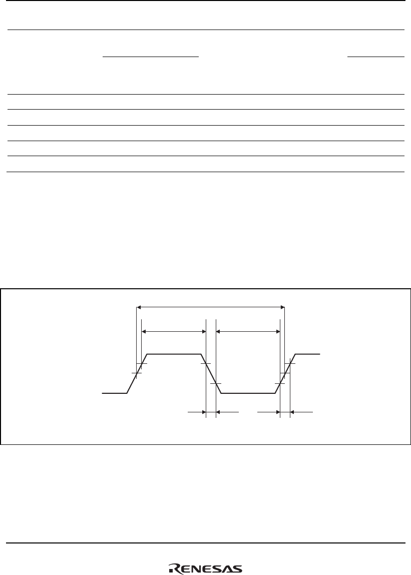
32. Electrical Characteristics
Rev.1.00 Jan. 10, 2008 Page 1569 of 1658
REJ09B0261-0100
Item Symbol Min. Max. Unit Figure
MODE13 to MODE11,
MODE8 to MODE5
tMDRH 20 ⎯ ns 32.6 MODE reset hold time
MODE14, MODE10,
MODE9, MODE4 to
MODE0
32.4
PRESET assert time tRESW 20 ⎯ t
cyc 32.4
PLL synchronization settling time tPLL 400 ⎯ μs 32.5
TRST reset hold time tTRSTRH 0 ⎯ ns 32.4
PRESET input rise time tPRr ⎯ 20 μs 32.6
PRESET input fall time tPRf ⎯ 20 μs 32.6
Notes: 1. With a crystal resonator connected on EXTAL and XTAL, the maximum frequency is 34
MHz. When using a third-order overtone crystal resonator, a tank circuit must be
connected externally.
2. The load capacitance connected on the CLKOUT pin should be not greater than 50 pF.
3. tcyc is the period of one CLKOUT clock cycle.
4. This applies to clock operating modes 0, 1, 2, and 3 (see table 15.2).
5. This applies to clock operating modes 8, 9, 10, and 11 (see table 15.2).
6. This applies to clock operating modes 16, 17, 18, and 19 (see table 15.2).
Note: When the clock is input from the EXTAL pin.
t
EXcyc
t
EXH
t
EXL
t
EXr
t
EXf
1/2V
DDQ
V
IH
V
IH
V
IL
V
IL
V
IH
1/2V
DDQ
Figure 32.1 EXTAL Clock Input Timing
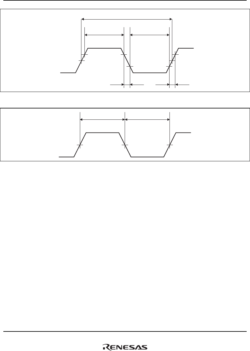
32. Electrical Characteristics
Rev.1.00 Jan. 10, 2008 Page 1570 of 1658
REJ09B0261-0100
t
CKOcyc
t
CKOH1
t
CKOL1
t
CKOr
t
CKOf
1/2V
DDQ
V
OH
V
OH
V
OL
V
OL
V
OH
1/2V
DDQ
Figure 32.2 CLKOUT Clock Output Timing (1)
t
CKOH2
1.5V 1.5V 1.5V
t
CKOL2
Figure 32.3 CLKOUT Clock Output Timing (2)
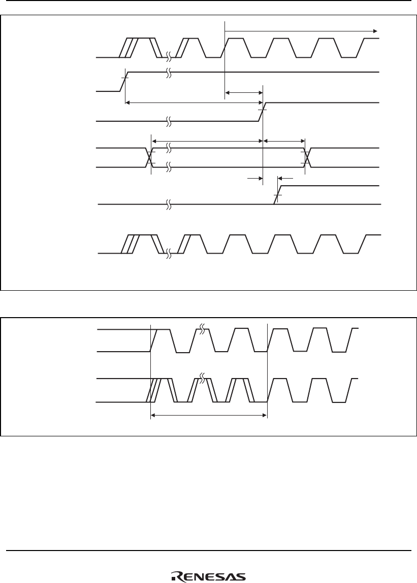
32. Electrical Characteristics
Rev.1.00 Jan. 10, 2008 Page 1571 of 1658
REJ09B0261-0100
VDD
t
OSC1
V
DD
min
t
MDRH
t
OSCMD
t
TRSTRH
t
RESW
CLKOUT
Notes: 1. Oscillation settling time for the case when the on-chip resonator is used
2. PLL2 is operating
PRESET
MODE14
MODE10
MODE9
MODE4 to MODE0
TRST
Oscillation settling time
Internal clock
Figure 32.4 Power-On Oscillation Settling Time
CLKOUT
output
EXTAL
input
t
PLL
Figure 32.5 PLL Synchronization Settling Time
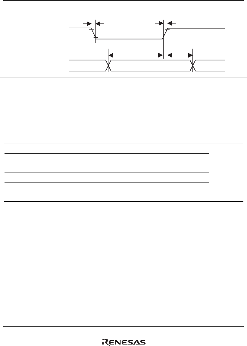
32. Electrical Characteristics
Rev.1.00 Jan. 10, 2008 Page 1572 of 1658
REJ09B0261-0100
t
MDRH
PRESET
MODE13 to MODE11
MODE8 to MODE5
t
MDRS
t
PRr
t
PRf
Figure 32.6 MODE Pin Setup/Hold Timing
32.3.2 Control Signal Timing
Table 32.7 Control Signal Timing
Conditions: VDDQ = 3.0 to 3.6 V, VDD = 1.1 V, Ta = −20 to +85/−40 to +85°C, CL = 30 pF
Item Symbol Min. Max. Unit Figure
BREQ setup time* t
BREQS 3 — ns
BREQ hold time tBREQH 1.5 — ns
BREQ delay time tBACKD — 6 ns
Bus tri-state delay time tBOFF1 — 12 ns
Bus buffer on time tBON1 — 12 ns
32.7
STATUS0, STATUS1 delay time tSTD — 6 ns 32.8
Note: * t
cyc is the period of one CLKOUT cycle.
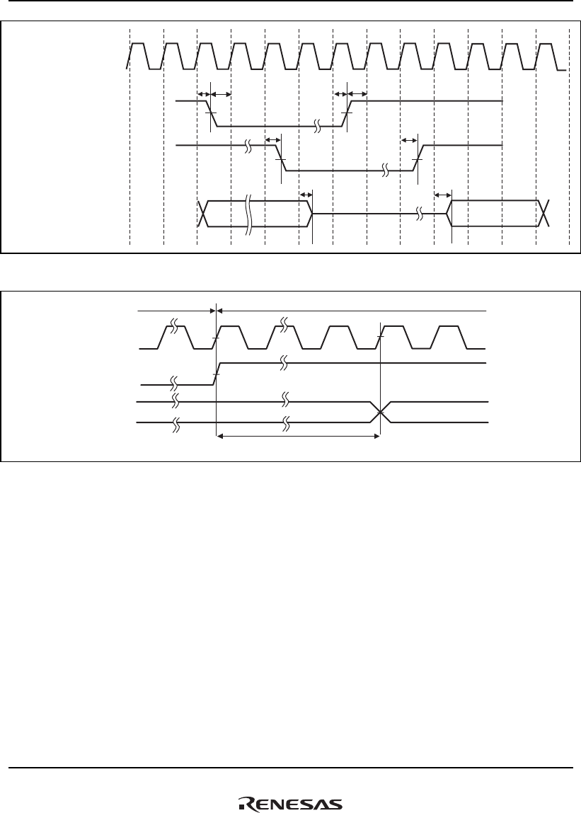
32. Electrical Characteristics
Rev.1.00 Jan. 10, 2008 Page 1573 of 1658
REJ09B0261-0100
t
BREQH
t
BREQS
t
BREQH
t
BREQS
t
BACKD
t
BACKD
t
BOFF1
t
BON1
CKIO
BREQ
BACK
A[25:0], CSn, BS,
RD/WR, CE2A, CE2B,
RAS, WEn, RD, CASn
Figure 32.7 Control Signal Timing
CLKOUT
t
STD
STATUS1
STATUS0 Reset
Power-on reset Normal operation
Normal
PRESET
Figure 32.8 STATUS Pin Output Timing at Power-On Reset

32. Electrical Characteristics
Rev.1.00 Jan. 10, 2008 Page 1574 of 1658
REJ09B0261-0100
32.3.3 Bus Timing
Table 32.8 Bus Timing
Conditions: VDDQ = 3.0 to 3.6 V, VDD = 1.1 V, Ta = −20 to +85/−40 to 85°C, CL = 30 pF
Item Symbol Min. Max. Unit Notes
Address delay time tAD 1.5 6 ns
BS delay time tBSD 1.5 6 ns
CS delay time tCSD 1.5 6 ns
R/W delay time tRWD 1.5 6 ns
RD delay time tRSD 1.5 6 ns
Read data setup time tRDS 2.5 ⎯ ns
Read data hold time tRDH 1.5 ⎯ ns
WE delay time (falling edge) tWEDF 1.5 6 ns Relative to CLKOUT falling edge
WE delay time tWED1 1.5 6 ns
Write data delay time tWDD 1.5 6 ns
RDY setup time tRDYS 2.5 ⎯ ns
RDY hold time tRDYH 1.5 ⎯ ns
FRAME delay time tFMD 1.5 6 ns MPX
IOIS16 setup time tIO16S 2.5 ⎯ ns PCMCIA
IOIS16 hold time tIO16H 1.5 ⎯ ns PCMCIA
IOWR delay time (falling edge) tICWSDF 1.5 6 ns PCMCIA
IORD delay time tICRSD 1.5 6 ns PCMCIA
DACK delay time tDACD 1.5 6 ns
DACK delay time (falling edge) tDACDF 1.5 6 ns Relative to CLKOUT falling edge
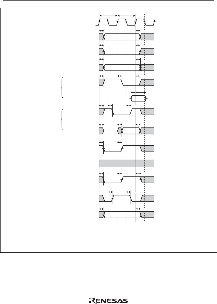
32. Electrical Characteristics
Rev.1.00 Jan. 10, 2008 Page 1575 of 1658
REJ09B0261-0100
CLKOUT
A25 to A0
CSn
RD
RD/WR
D31 to D0
D31 to D0
(Write)
(Read)
DACKn
(SA: IO ← memory)
(SA: IO → memory)
DACKn
DACKn
(DA)
Legend:
IO: DACK device
SA: Single-address DMA transfer
DA: Dual-address DMA transfer
Note: DACK is configured as active-high.
T1 T2
tAD
t
AD
WEn
BS
RDY
t
DACD
t
DACD
t
DACD
t
DACD
t
DACDF
t
DACDF
t
DACD
t
WDD
t
WDD
t
WDD
t
BSD
t
BSD
t
WED1
t
WEDF
t
WEDF
t
RDH
t
RDS
t
RSD
t
RSD
t
RSD
t
CSD
t
CSD
t
RWD
t
RWD
Figure 32.9 SRAM Bus Cycle: Basic Bus Cycle (No Wait)
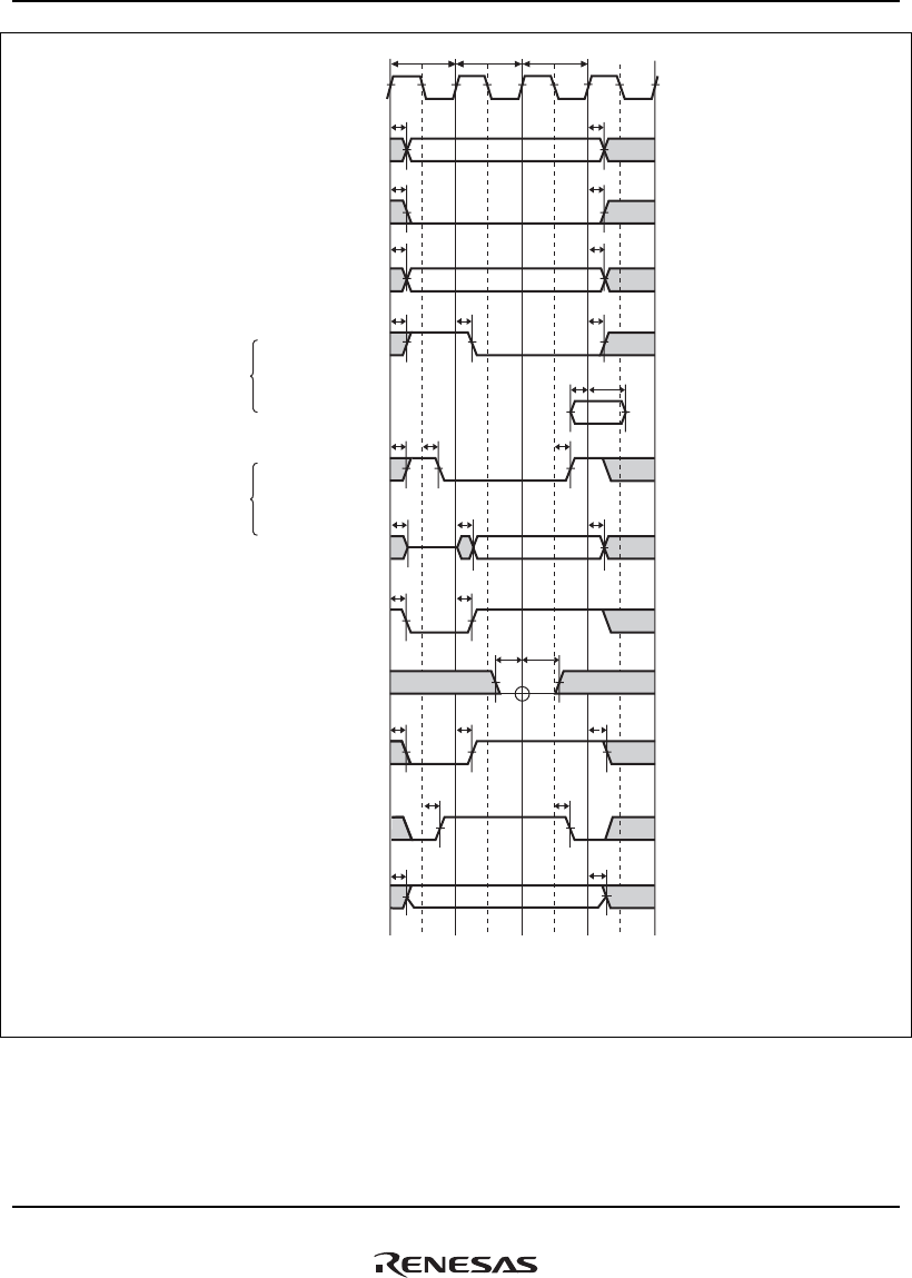
32. Electrical Characteristics
Rev.1.00 Jan. 10, 2008 Page 1576 of 1658
REJ09B0261-0100
A25 to A0
D31 to D0
D31 to D0
(Write)
(Read)
(SA: IO ← memory)
(SA: IO → memory)
Legend
:
IO: DACK device
SA: Single-address DMA transfer
DA: Dual-address DMA transfer
Note: DACK is configured as active-high.
t
WDD
t
WDD
t
WDD
t
DACDF
t
DACDF
CLKOUT
CSn
RD
WEn
BS
RDY
RD/WR
DACKn
(DA)
T1
t
AD
Tw T2
t
AD
t
RDH
t
RDS
t
CSD
t
RWD
t
RWD
t
CSD
t
RSD
t
RSD
t
RSD
t
WED1
t
WEDF
t
WEDF
t
RDYH
t
RDYS
t
BSD
t
BSD
t
DACD
t
DACD
t
DACD
t
DACD
t
DACD
DACKn
DACKn
Figure 32.10 SRAM Bus Cycle: Basic Bus Cycle (One Internal Wait Cycle)
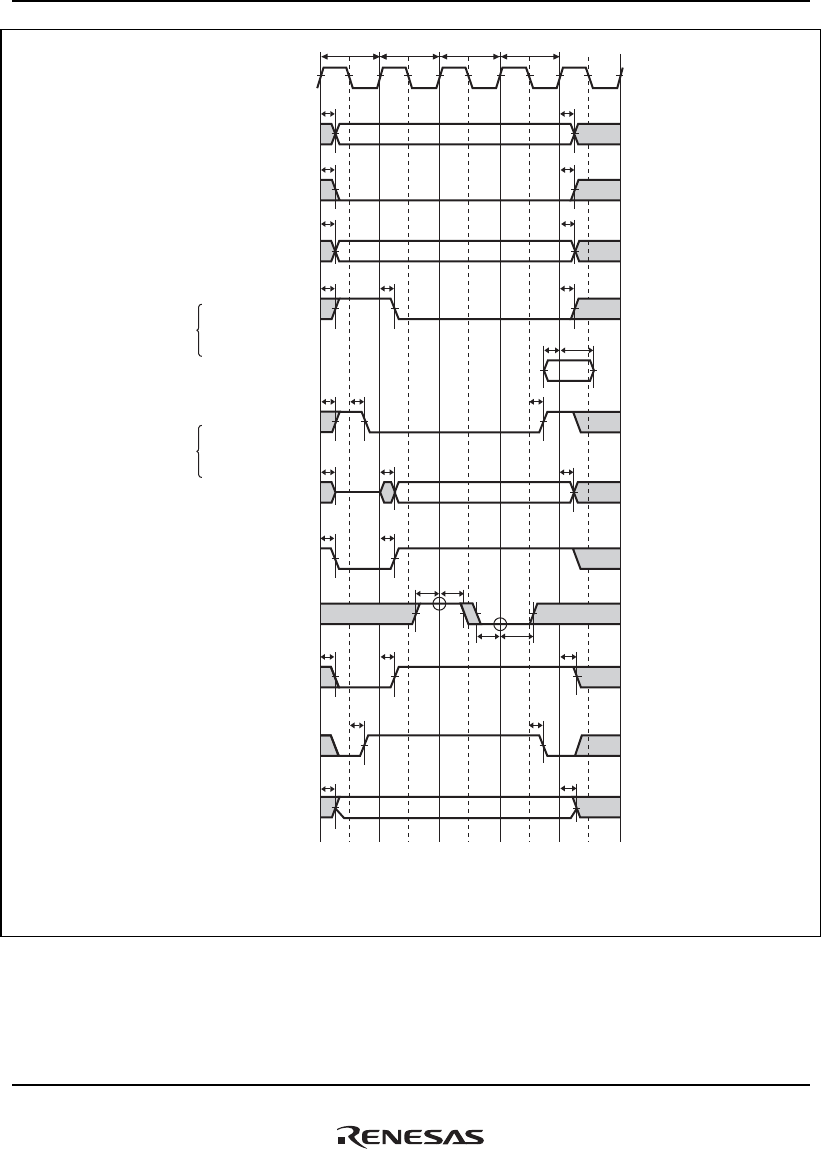
32. Electrical Characteristics
Rev.1.00 Jan. 10, 2008 Page 1577 of 1658
REJ09B0261-0100
A25 to A0
D31 to D0
D31 to D0
(Write)
(Read)
(SA: IO ← memory)
(SA: IO → memory)
Legend:
IO: DACK device
SA: Single-address DMA transfer
DA: Dual-address DMA transfer
Note: DACK is configured as active-high.
t
WDD
t
WDD
t
WDD
t
DACDF
t
DACDF
CLKOUT
RD/WR
RD
CSn
RDY
BS
WEn
DACKn
(DA)
T1
t
AD
Tw Twe T2
t
AD
t
RDH
t
RDS
t
CSD
t
RWD
t
RWD
t
CSD
t
RSD
t
RSD
t
RSD
t
WED1
t
WEDF
t
WEDF
t
RDYH
t
RDYS
t
RDYH
t
RDYS
t
BSD
t
BSD
t
DACD
t
DACD
t
DACD
t
DACD
t
DACD
DACKn
DACKn
Figure 32.11 SRAM Bus Cycle: Basic Bus Cycle
(One Internal Wait Cycle + One External Wait Cycle)
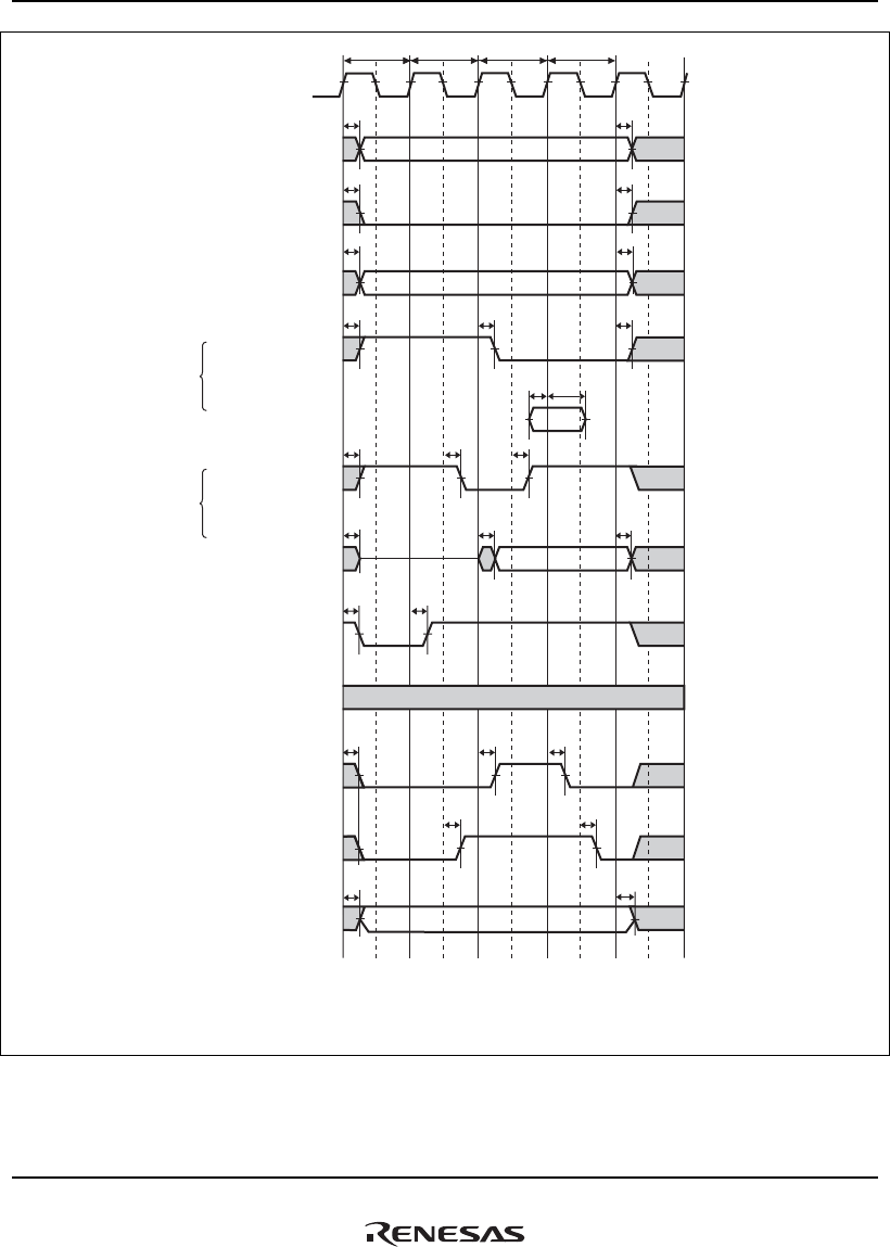
32. Electrical Characteristics
Rev.1.00 Jan. 10, 2008 Page 1578 of 1658
REJ09B0261-0100
A25 to A0
D31 to D0
D31 to D0
(Write)
(Read)
(SA: IO ← memory)
(SA: IO → memory)
Legend:
IO: DACK device
SA: Single-address DMA transfer
DA: Dual-address DMA transfer
Note: DACK is configured as active-high.
t
WDD
t
WDD
t
WDD
t
DACDF
t
DACDF
t
DACD
t
DACD
t
DACD
TS1
t
AD
T1 T2 TH1
t
AD
t
RDH
t
RDS
t
CSD
t
RWD
t
RWD
t
CSD
t
RSD
t
RSD
t
RSD
t
WED1
t
WEDF
t
WEDF
t
BSD
t
BSD
t
DACD
t
DACD
CLKOUT
RD/WR
CSn
WEn
BS
RDY
RD
DACKn
DACKn
DACKn
(DA)
Figure 32.12 SRAM Bus Cycle: Basic Bus Cycle (CSnWCR.IW = 0000,
CSnWCR.RDS = 001, CSnWCR.WTS = 001, CSnWCR.RDH = 001, CSnWCR.WTH = 001)
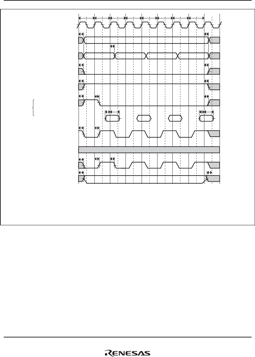
32. Electrical Characteristics
Rev.1.00 Jan. 10, 2008 Page 1579 of 1658
REJ09B0261-0100
D31 to D0
(Read)
(SA: IO ← memory)
Legend:
IO: DACK device
SA: Single-address DMA transfer
DA: Dual-address DMA transfer
Note: DACK is configured as active-high.
CLKOUT
A25 to A5
T1 T2
RD/WR
CSn
BS
RDY
RD
A4 to A0
TB2 TB1 TB2 TB1 TB2 TB1
tCSD
tAD
tRWD
tBSD
tRDS
tBSD
tRSD
tRSD
tRDH
tAD tAD
tCSD
tRWD
tRDH
tRSD
tRDS
DACKn
DACKn
(DA)
tDACD tDACD
tDACD
t
DACD
tDACD
Figure 32.13 Burst ROM Bus Cycle (No Wait)
32. Electrical Characteristics
Rev.1.00 Jan. 10, 2008 Page 1580 of 1658
REJ09B0261-0100
D31 to D0
(Read)
(SA: IO ← memory)
Legend:
IO: DACK device
SA: Single-address DMA transfer
DA: Dual-address DMA transfer
Note: DACK is configured as active-high.
A25 to A5
A4 to A0
T1 T2TB2 TB1 TB2 TB1 TB2 TB1Twb Twb TwbTweTw
tAD
tCSD
tRSD
tRDH
tRDS
tBSD
tAD
tRDH
tRSD
tRDS
tAD
tCSD
tRDYH
tRDYS
tRDYH
tRDYS
tRDYH
tRDYS
tDACD tDACD
tDACD tDACD
tRWD tRWD
CLKOUT
CSn
RD/WR
BS
RDY
RD
DACKn
DACKn
(DA)
Figure 32.14 Burst ROM Bus Cycle (One Internal Wait Cycle + One External Wait Cycle
for the 1st Datum; One Internal Wait Cycle for the 2nd, 3rd, and 4th Data)
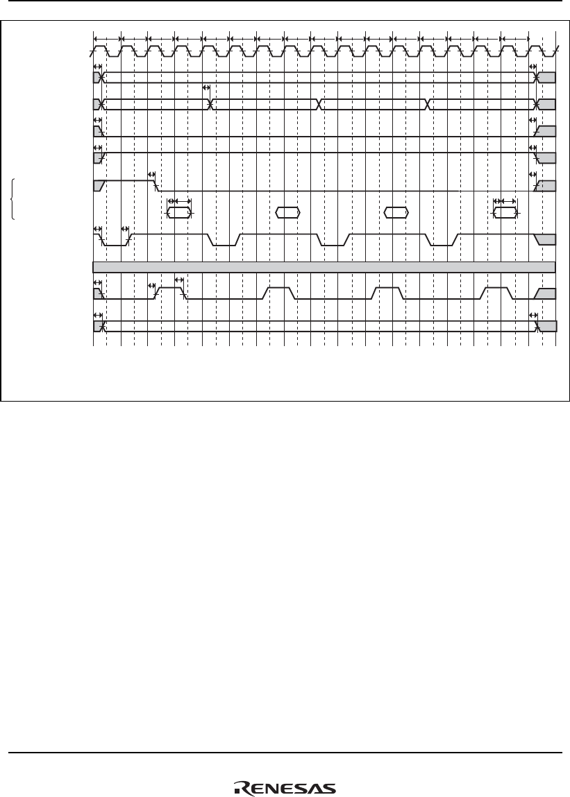
32. Electrical Characteristics
Rev.1.00 Jan. 10, 2008 Page 1581 of 1658
REJ09B0261-0100
D31 to D0
(Read)
(SA: IO ← memory)
Legend:
IO: DACK device
SA: Single-address DMA transfer
DA: Dual-address DMA transfer
Note: DACK is configured as active-high.
A25 to A5
A4 to A0
T1 TB2
t
CSD
t
RWD
t
BSD
t
RDS
t
BSD
t
RSD
t
AD
TS1
t
DACD
TB1 TB2
t
AD
t
RDH
t
DACD
t
DACD
TB1 TB2 T2TB1
t
AD
t
CSD
t
RWD
t
RDH
t
RSD
t
RDS
TH1TS1TH1 TS1TH1 TS1TH1
CLKOUT
DACKn
(DA)
DACKn
CSn
RD/WR
RD
BS
RDY
t
DACD
t
DACD
Figure 32.15 Burst ROM Bus Cycle (CSnWCR.IW = 0000, CSnWCR.RDS = 001,
CSnWCR.WTS = 001, CSnWCR.RDH = 001, CSnWCR.WTH = 001)
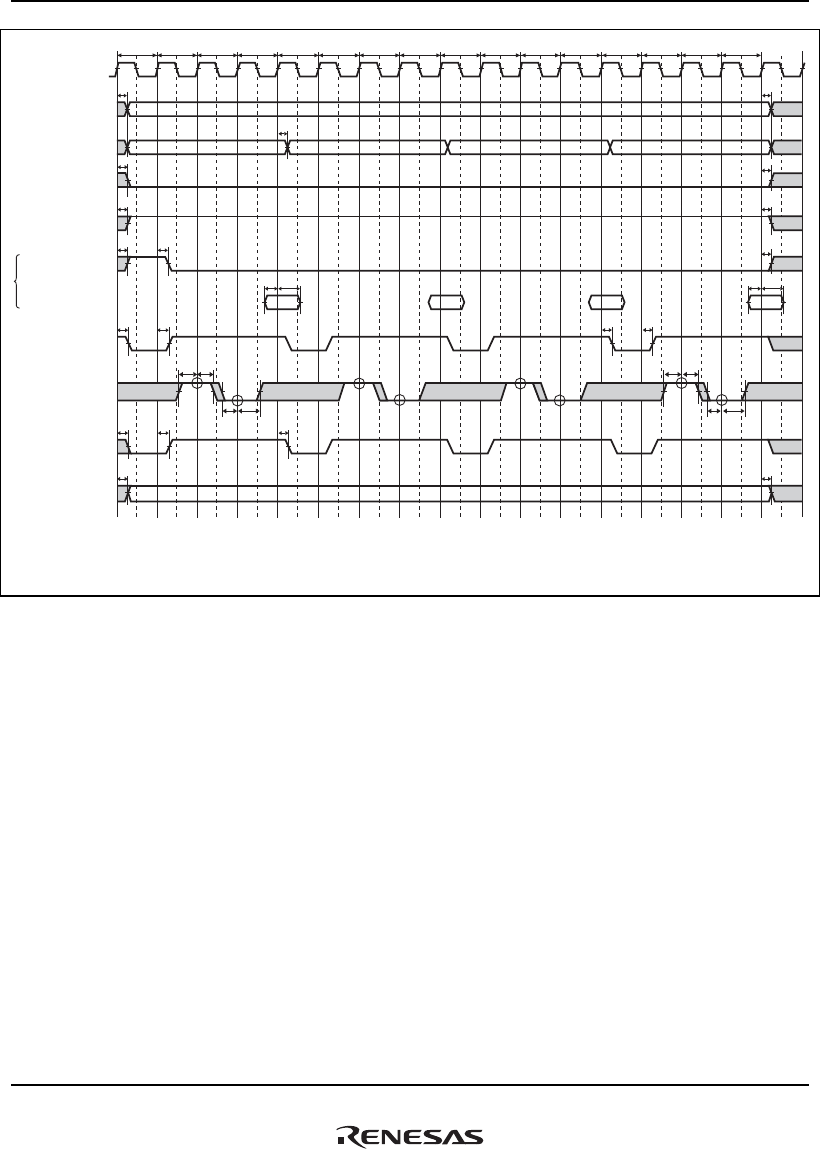
32. Electrical Characteristics
Rev.1.00 Jan. 10, 2008 Page 1582 of 1658
REJ09B0261-0100
D31 to D0
(Read)
(SA: IO ← memory)
Legend:
IO: DACK device
SA: Single-address DMA transfer
DA: Dual-address DMA transfer
Note: DACK is configured as active-high.
A25 to A5
A4 to A0
TwT1 Twe TB2 TB1 Twb Twbe TB1
TB2 Twb TwbeTwb T2TB2Twbe TB1
t
AD
t
AD
t
AD
t
RDH
t
RDS
t
RDH
t
RDS
t
DACD
t
DACD
t
DACD
t
BSD
t
BSD
t
BSD
t
BSD
t
RSD
t
RSD
t
RWD
t
CSD
t
RWD
t
CSD
t
DACD
t
DACD
t
RSD
t
RDYH
t
RDYS
t
RDYH
t
RDYS
t
RDYH
t
RDYS
t
RDYH
t
RDYS
CLKOUT
DACKn
(DA)
DACKn
CSn
RD/WR
RD
BS
RDY
Figure 32.16 Burst ROM Bus Cycle (One Internal Wait Cycle + One External Wait Cycle)
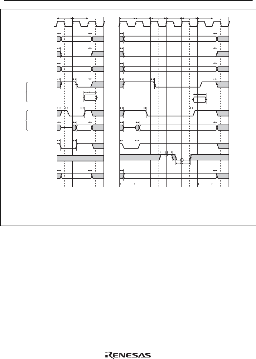
32. Electrical Characteristics
Rev.1.00 Jan. 10, 2008 Page 1583 of 1658
REJ09B0261-0100
D15 to D0
D15 to D0
(Write)
(Read)
Legend:
IO: DACK device
SA: Single-address DMA transfer
DA: Dual-address DMA transfer
Note: DACK is configured as active-high.
Tpcm1 Tpcm2 Tpcm0 Tpcm1 Tpcm2Tpcm1wTpcm1w Tpcm2w
tAD tAD
tWDD
tBSD tBSD
tBSD tBSD
tWDD tWDD
tRWD
tCSD tCSD
tRWD
tRSD
tRSD tRSD
tWEDF
tWED1 tWEDF
tDACD
tRDH
tRDS
tRDYH
tRDYS
tRDYH
tRDYS
tDACD
tAD tAD
tWDD
tWDD tWDD
tRWD
tCSD tCSD
tRWD
tRSD
tRSD tRSD
tWEDF
tWED1 tWEDF
tDACD
TED TEH
tRDH
tRDS
tDACD
A25 to A0
CLKOUT
CExx
REG (WE0)
RD/WR
WE1
RD
BS
RDY
DACKn
(DA)
(1) TED = 0, THE = 0, no wait (2) TED = 1, THE = 1, one internal wait + one external wait cycles
Figure 32.17 PCMCIA Memory Bus Cycle
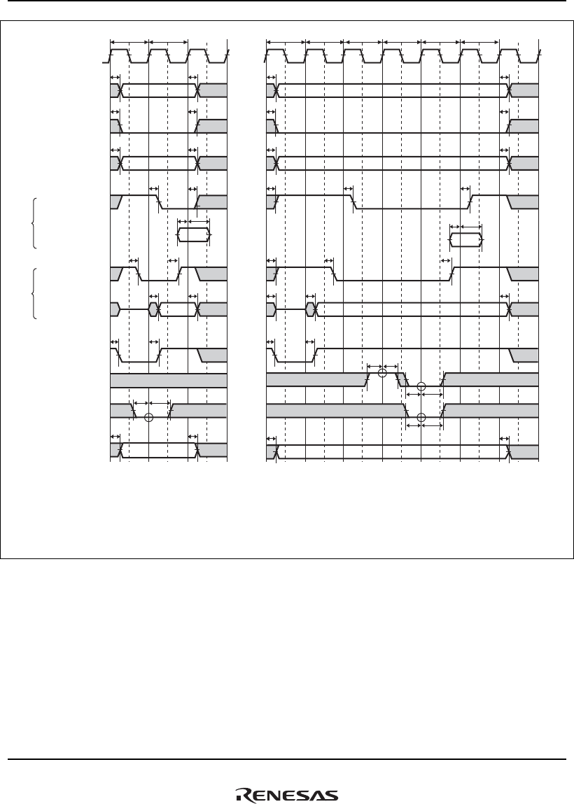
32. Electrical Characteristics
Rev.1.00 Jan. 10, 2008 Page 1584 of 1658
REJ09B0261-0100
D15 to D0
D15 to D0
(Write)
(Read)
Legend:
IO: DACK device
SA: Single-address DMA transfer
DA: Dual-address DMA transfer
Note: DACK is configured as active-high.
A25 to A0
Tpci1 Tpci2 Tpci0 Tpci1 Tpci2
Tpci1wTpci1w Tpci2w
CLKOUT
tAD tAD
tBSD tBSD
tBSD tBSD
tWDD tWDD
tRWD
tCSD tCSD
tRWD
tICRSD tICRSD
tICWSDF tICWSDF
tDACD
tRDH
tRDS
tRDYH
tRDYS
tRDYH
tRDYS
tIO16H
tIO16S
tIO16H
tIO16S
tDACD
tAD tAD
tWDD
tWDD tWDD
tRWD
tCSD tCSD
tRWD
tICRSD
tICRSD tICRSD
tICWSDF
tICWSDF tICWSDF
tDACD
tRDH
tRDS
tDACD
(1) TED = 0, THE = 0, no wait (2) TED = 1, THE = 1, internal wait + external wait cycles
CExx
REG (WE0)
RD/WR
ICIOWR (WE2)
ICIORD (WE3)
BS
RDY
IOIS16
DACKn
(DA)
Figure 32.18 PCMCIA I/O Bus Cycle
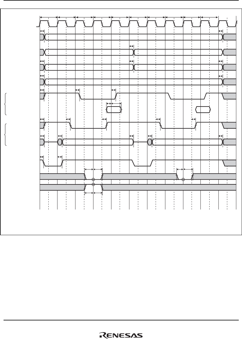
32. Electrical Characteristics
Rev.1.00 Jan. 10, 2008 Page 1585 of 1658
REJ09B0261-0100
Tpci0 Tpci1 Tpci2w
Tpci2Tpci1w Tpci0 Tpci1 Tpci2w
Tpci2Tpci1w
CLKOUT
CExx
REG (WE0)
A0
RD/WR
ICIOWR (WE2)
ICIORD (WE2)
BS
RDY
IOIS16
t
BSD
t
BSD
t
AD
t
AD
t
WDD
t
WDD
t
WDD
t
WDD
t
WDD
t
RWD
t
RWD
t
AD
t
CSD
t
CSD
t
CSD
t
ICRSD
t
ICRSD
t
ICRSD
t
ICWSDF
t
ICWSDF
t
ICWSDF
t
ICWSDF
t
ICWSDF
t
RDH
t
RDS
t
RDYS
t
RDYS
t
IO16S
t
IO16H
t
RDYS
t
RDYH
D15 to D0
D15 to D0
(Write)
(Read)
Legend:
IO: DACK device
SA: Single-address DMA transfer
DA: Dual-address DMA transfer
Note: DACK is configured as active-high.
A25 to A1
Figure 32.19 PCMCIA I/O Bus Cycle
(TED = 1, TEH = 1, One Internal Wait Cycle, with Bus Sizing)
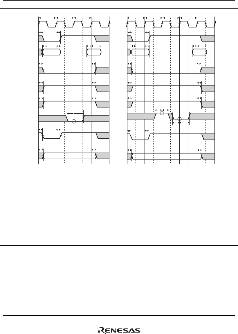
32. Electrical Characteristics
Rev.1.00 Jan. 10, 2008 Page 1586 of 1658
REJ09B0261-0100
Tm1 Tmd1w Tmd1 Tm0 Tmd1w Tmd1Tmd1w
CLKOUT
RD/FRAME
RD/WR
WEn
RDY
BS
D31 to D0
CSn
DACKn
(DA)
t
FMD
t
FMD
t
BSD
t
BSD
t
BSD
t
BSD
t
CSD
t
CSD
t
DACD
t
RDH
t
RDS
D0
t
RDYH
t
RDYS
t
DACD
t
RWD
t
RWD
t
WED1
t
WED1
t
FMD
t
FMD
t
CSD
t
CSD
t
RDH
t
RDS
t
WDD
t
WDD
t
WDD
A D0A
t
WDD
t
RWD
t
RWD
t
WED1
t
WED1
t
DACD
t
DACD
t
RDYH
t
RDYS
tRDYH
t
RDYS
(1) 1st data: One internal wait cycle
Information in the first data bus cycle
D31 to D29: Access size
000: Byte
001: Word (2 bytes)
010: Longword (4 bytes)
011: Quadword (8 bytes)
1xx: Burst (32 bytes)
D25 to D0: Address
(2) 1st data: One internal wait + one external wait cycles
Information in the first data bus cycle
D31 to D29: Access size
000: Byte
001: Word (2 bytes)
010: Longword (4 bytes)
011: Quadword (8 bytes)
1xx: Burst (32 bytes)
D25 to D0: Address
Legend:
IO: DACK device
SA: Single-address DMA transfer
DA: Dual-address DMA transfer
Note: DACK is configured as active-high.
Figure 32.20 MPX Basic Bus Cycle (Read)
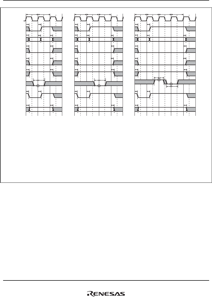
32. Electrical Characteristics
Rev.1.00 Jan. 10, 2008 Page 1587 of 1658
REJ09B0261-0100
Tm1 Tmd1w Tmd1
t
FMD
t
FMD
t
BSD
t
BSD
t
CSD
t
CSD
t
DACD
t
RDYH
t
RDYS
t
DACD
t
WED1
t
WED1
Tm1 Tmd1
t
FMD
t
FMD
t
BSD
t
BSD
t
CSD
t
CSD
t
DACD
D0 D0
t
RDYH
t
RDYS
t
DACD
t
RWD
t
RWD
t
RWD
t
RWD
t
WED1
t
WED1
A
t
RDYH
t
RDYS
t
RDYH
t
RDYS
t
WDD
t
WDD
t
WDD
A
t
WDD
t
WDD
t
WDD
Tm1 Tmd1w Tmd1w Tmd1
t
FMD
t
FMD
t
BSD
t
BSD
t
CSD
t
CSD
t
DACD
t
DACD
t
WED1
t
WED1
D0
t
RWD
t
RWD
A
t
WDD
t
WDD
t
WDD
CLKOUT
RD/FRAME
RD/WR
WEn
RDY
BS
CSn
DACKn
(DA)
D31 to D0
(1) 1st data: No wait
Information in the first data bus cycle
D31 to D29: Access size
000: Byte
001: Word (2 bytes)
010: Longword (4 bytes)
011: Quadword (8 bytes)
1xx: Burst (32 bytes)
D25 to D0: Address
(2) 1st data: One internal wait cycle
Information in the first data bus cycle
D31 to D29: Access size
000: Byte
001: Word (2 bytes)
010: Longword (4 bytes)
011: Quadword (8 bytes)
1xx: Burst (32 bytes)
D25 to D0: Address
(3) 1st data: One internal wait + one external wait cycles
Information in the first data bus cycle
D31 to D29: Access size
000: Byte
001: Word (2 bytes)
010: Longword (4 bytes)
011: Quadword (8 bytes)
1xx: Burst (32 bytes)
D25 to D0: Address
Legend:
IO: DACK device
SA: Single-address DMA transfer
DA: Dual-address DMA transfer
Note: DACK is configured as active-high.
Figure 32.21 MPX Basic Bus Cycle (Write)

32. Electrical Characteristics
Rev.1.00 Jan. 10, 2008 Page 1588 of 1658
REJ09B0261-0100
D31 to D0
(2) 1st data: No internal wait, 2nd to 8th data: No internal wait + external wait control
Information in the first data bus cycle
D31 to D29: Access size
000: Byte
001: Word (2 bytes)
010: Longword (4 bytes)
011: Quadword (8 bytes)
1xx: Burst (32 bytes)
D25 to D0: Address
D31 to D0
(1) 1st data: One internal wait cycle, 2nd to 8th data: No waitl
Information in the first data bus cycle
D31 to D29: Access size
000: Byte
001: Word (2 bytes)
010: Longword (4 bytes)
011: Quadword (8 bytes)
1xx: Burst (32 bytes)
D25 to D0: Address
Legend:
IO: DACK device
SA: Single-address DMA transfer
DA: Dual-address DMA transfer
Note: DACK is configured as active-high.
Tm1
CLKOUT
RD/FRAME
CSn
RD/WR
RDY
BS
DACKn
(DA)
CLKOUT
RD/FRAME
CSn
RD/WR
RDY
BS
DACKn
(DA)
t
FMD
Tmd1w Tmd1 Tmd2 Tmd3 Tmd4 Tmd5 Tmd6 Tmd7 Tmd8
D1
A D2 D3 D4 D5 D6 D7 D8
t
FMD
t
WDD
t
CSD
t
CSD
t
RWD
t
RDYS
t
RDYH
t
RWD
t
DACD
t
DACD
t
WDD
t
BSD
t
BSD
t
RDH
t
RDS
Tm1
t
FMD
Tmd1w Tmd1 Tmd2w Tmd2 Tmd3 Tmd7 Tmd8w Tmd8
D1
A D3 D4 D6 D8
t
FMD
t
WDD
t
CSD
t
CSD
t
RWD
t
RDYS
t
RDYH
t
RWD
t
DACD
t
DACD
t
WDD
t
BSD
t
BSD
t
RDH
t
RDS
t
RDYS
t
RDYH
Figure 32.22 MPX Bus Cycle (Burst Read)
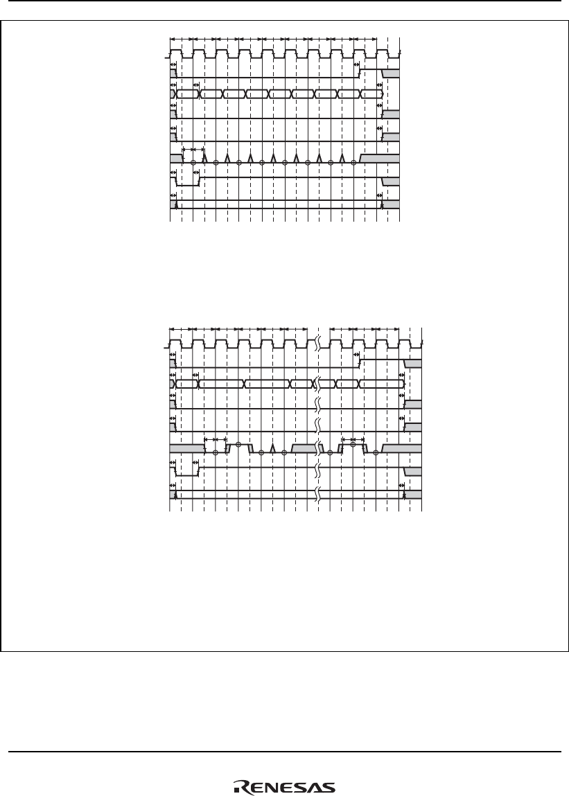
32. Electrical Characteristics
Rev.1.00 Jan. 10, 2008 Page 1589 of 1658
REJ09B0261-0100
D31 to D0
(2) 1st data: One internal wait cycle, 2nd to 8th data: No internal wait + external wait control
Information in the first data bus cycle
D31 to D29: Access size
000: Byte
001: Word (2 bytes)
010: Longword (4 bytes)
011: Quadword (8 bytes)
1xx: Burst (32 bytes)
D25 to D0: Address
D31 to D0
(1) No internal wait
Information in the first data bus cycle
D31 to D29: Access size
000: Byte
001: Word (2 bytes)
010: Longword (4 bytes)
011: Quadword (8 bytes)
1xx: Burst (32 bytes)
D25 to D0: Address
Legend:
IO: DACK device
SA: Single-address DMA transfer
DA: Dual-address DMA transfer
Note: DACK is configured as active-high.
Tm1
CLKOUT
RD/FRAME
CSn
RD/WR
RDY
BS
DACKn
(DA)
CLKOUT
RD/FRAME
CSn
RD/WR
RDY
BS
DACKn
(DA)
t
FMD
Tmd1 Tmd2 Tmd3 Tmd4 Tmd5 Tmd6 Tmd7 Tmd8
A D1 D2 D3 D4 D5 D6 D7 D8
t
FMD
t
WDD
t
CSD
t
CSD
t
RWD
t
RDYS
t
RDYH
t
RWD
t
DACD
t
DACD
t
WDD
t
WDD
t
BSD
t
BSD
Tm1
t
FMD
Tmd1w Tmd1 Tmd2w Tmd2 Tmd3 Tmd7 Tmd8w Tmd8
AD1 D2 D8D3 D7
t
FMD
t
WDD
t
CSD
t
CSD
t
RWD
t
RDYS
t
RDYH
t
RWD
t
DACD
t
DACD
t
WDD
t
BSD
t
BSD
t
WDD
t
RDYS
t
RDYH
Figure 32.23 MPX Bus Cycle (Burst Write)
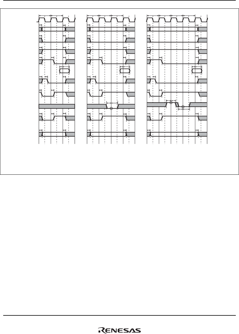
32. Electrical Characteristics
Rev.1.00 Jan. 10, 2008 Page 1590 of 1658
REJ09B0261-0100
A25 to A0
D31 to D0
(Read)
(SA: IO ← memory)
Legend:
IO: DACK device
SA: Single-address DMA transfer
DA: Dual-address DMA transfer
Note: DACK is configured as active-high.
T1 Tw T2
t
DACD
t
DACD
t
CSD
t
CSD
t
DACD
t
RDYH
t
RDYS
t
DACD
t
DACD
t
RWD
t
RWD
T1 T2
t
DACD
t
DACD
t
CSD
t
CSD
t
DACD
t
DACD
t
WED1
t
DACD
t
RWD
t
RWD
t
RDYH
t
RDYS
t
RDYH
t
RDYS
t
AD
t
AD
t
AD
t
AD
T1 Tw Twe T2
t
DACD
t
DACD
t
RSD
t
RSD
t
RSD
t
RSD
t
RSD
t
RSD
t
RSD
t
RSD
t
WED1
t
WED1
t
WEDF
t
WED1
t
WEDF
t
WED1
t
WEDF
t
WED1
t
CSD
t
CSD
t
DACD
t
BSD
t
BSD
t
BSD
t
BSD
t
BSD
t
BSD
t
DACD
t
DACD
t
RWD
t
RWD
t
RSD
t
AD
t
AD
t
RDH
t
RDS
t
RDH
t
RDS
t
RDH
t
RDS
CLKOUT
RD
RD/WR
WEn
RDY
BS
CSn
DACKn
(DA)
DACKn
(1) Basic read cycle (no wait) (2) Basic read cycle (one internal wait cycle) (3) Basic read cycle (one internal wait + one external wait cycles)
t
Figure 32.24 Memory Byte Control SRAM Bus Cycle
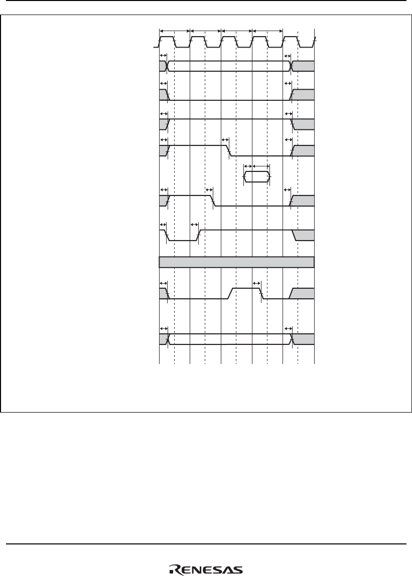
32. Electrical Characteristics
Rev.1.00 Jan. 10, 2008 Page 1591 of 1658
REJ09B0261-0100
A25 to A0
D31 to D0
(Read)
(SA: IO ← memory)
Legend:
IO: DACK device
SA: Single-address DMA transfer
DA: Dual-address DMA transfer
Note: DACK is configured as active-high.
CLKOUT
RD/WR
CSn
RD
WEn
BS
RDY
DACKn
(DA)
TS1 T1 T2 TH1
t
RSD
t
RSD
t
WED1
t
WEDF
t
WED1
t
CSD
t
CSD
t
DACD
t
BSD
t
BSD
t
DACD
t
RWD
t
RWD
t
RSD
t
AD
t
AD
t
RDH
t
RDS
DACKn
t
DACD
t
DACD
Figure 32.25 Memory Byte Control SRAM Bus Cycle: Basic Read Cycle
(CSnWCR.IW = 0000, CSnWCR.RDS = 001, CSnWCR.WTS = 001, CSnWCR.RDH = 001,
CSnWCR.WTH = 001)

32. Electrical Characteristics
Rev.1.00 Jan. 10, 2008 Page 1592 of 1658
REJ09B0261-0100
32.3.4 DBSC2 Signal Timing
Table 32.9 DBSC2 Signal Timing
Conditions: VDD-DDR= 1.7 to 1.9 V, Vref= 0.9 V, VDD= 1.1 V, Ta= −20 to +85/−40 to 85°C,
CL= 30 pF, ODT=on), Drive Strength=Normal
Item Symbol Min. Max. Unit Figure Notes
MCK output cycle tCK 3.33 5.0 ns
MCK output high-level pulse
width
tCH 0.45 0.55 tMCK
MCK output low-level pulse
width
tCL 0.45 0.55 tMCK
880 — ps DDR2-600 Address and control signal
setup time to MCK rising edge
tIS
1290 DDR2-400
880 — ps DDR2-600 Address and control signal hold
time to MCK rising edge
tIH
1290 DDR2-400
Address and control signal
width
tIPW 0.6 — tMCK
MCLK-to-MDQS skew time
(Read)
tRDQSDLY −0.2 1.4 ns
MDQS high-level pulse width
(Read)
tRDQSH 0.35 0.65 tMCK
MDQS low-level pulse width
(Read)
tRDQSL 0.35 0.65 tMCK
MDQS preamble (Read) tRPRE 0.9 1.1 tMCK
MDQS postamble (Read) tRPST 0.4 0.6 tMCK
−390 390 DDR2-600 MDQS-to-MDQ skew time
(Read)
tRDQSQ
−590 590
ps
DDR2-400
MDQ signal hold time to DQS
(Read)
tRQH 0.45 × tMCK
−470
— ps DDR2-600
0.45 × tMCK
−630
— DDR2-400
32. Electrical Characteristics
Rev.1.00 Jan. 10, 2008 Page 1593 of 1658
REJ09B0261-0100
Item Symbol Min. Max. Unit Figure Notes
Write command to first
MDQS delay time
(Rising edge)
tWDQSS WL
−0.18
WL
+0.18
tMCK
MDQS falling edge
setup time to MCK
rising edge (Write)
tWDSS 0.27 — tMCK
MDQS falling edge hold
time to MCK rising edge
(Write)
tWDSH 0.27 — tMCK
MDQS high-level pulse
width (Write)
tWDQSH 0.35 0.9 tMCK
MDQS low-level pulse
width (Write)
tWDQSL 0.35 0.9 tMCK
MDQS preamble (Write) tWPRE 0.35 — tMCK
MDQS postamble
(write)
tWPST 0.4 — tMCK
430 DDR2-600 MDQ/MDM setup time
to MDQS (Write)
tWDS
630 —
ps
DDR2-400
430 DDR2-600 MDQ/MDM hold time to
MDQS (Write)
tWDH
630 —
ps
DDR2-400
MDQ/MDM signal width
(Write)
tWDIPW 0.35 — tMCK
MDQ high-impedance
time from MDQS (Write)
tHZ t
WDH tMCK ns
Note: tMCK: one MCK cycle time
t
CK
t
CH
t
CL
MCK0, MCK1
MCK0, MCK1
Figure 32.26 MCK Output Clock

32. Electrical Characteristics
Rev.1.00 Jan. 10, 2008 Page 1594 of 1658
REJ09B0261-0100
MCK0, MCK1 (solid line)
MCK0, MCK1 (dotted line)
tIH
MCKE, MCS,
MRAS, MCAS,
MWE, MBA[2:0],
MA[14:0]
tIS
tIPW
Figure 32.27 Command Signal and MCK Output Clock
MCK0, MCK1 (solid line)
MCK0, MCK1 (dotted line)
MCKE, MCS,
MRAS, MCAS,
MWE, MBA[2:0],
MA[14:0]
READ
Command
MDQS[3:0] (solid line)
MDQS[3:0] (dotted line)
tRDQSCK (Min.)
MDQS[3:0] (solid line)
MDQS[3:0] (dotted line)
tRDQSCK (Max.)
tRDQSCK (min)
tRDQSCK (min)
tRDQSCK (max)
tRDQSCK (max)
CL (Cas Latency)
Figure 32.28 MDQS Input Timing at Data Read
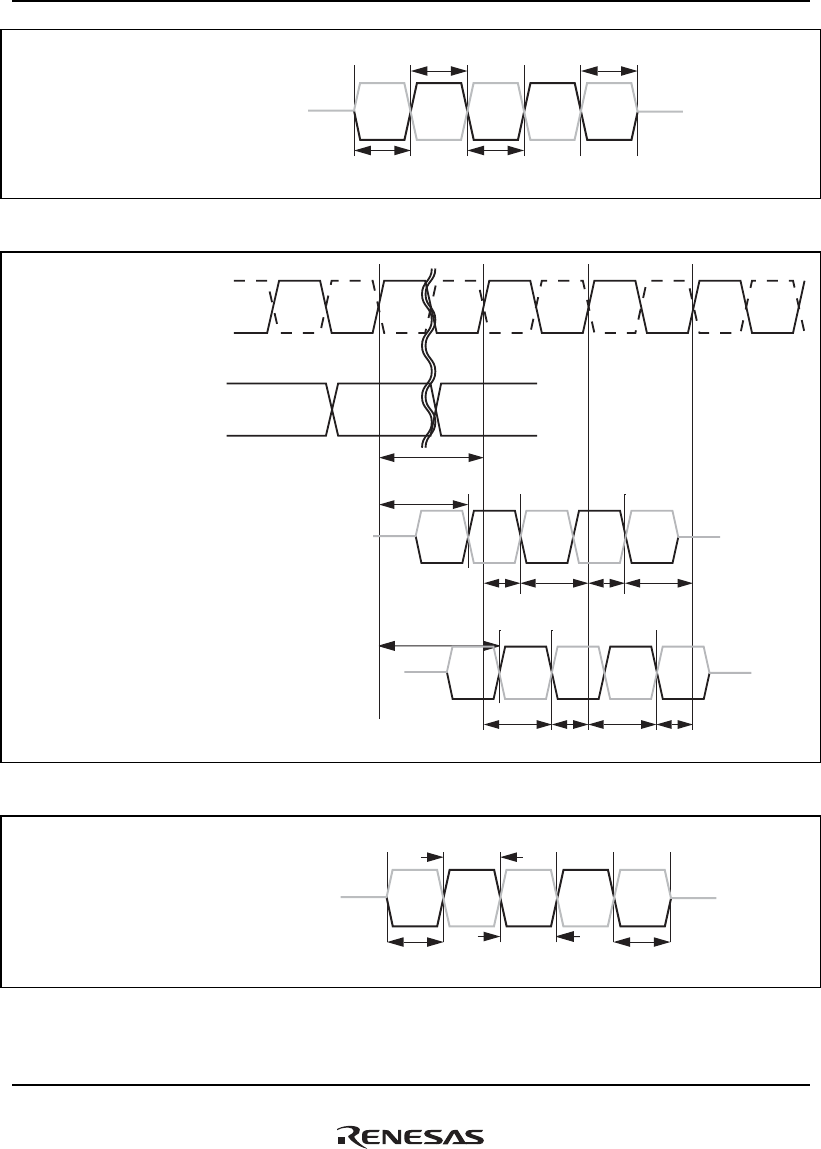
32. Electrical Characteristics
Rev.1.00 Jan. 10, 2008 Page 1595 of 1658
REJ09B0261-0100
MDQS[3:0] (solid line)
MDQS[3:0] (dotted line)
t
RDQSH
t
RPRE
t
RPST
t
RDQSL
HiZ HiZ
Figure 32.29 Restriction of MDQS Input Waveform (Read)
WRITE
Command
MDQS[3:0] (solid line)
MDQS[3:0] (dotted line)
tWDQSS (Min.)
MDQS[3:0] (solid line)
MDQS[3:0] (dotted line)
tWDQSS (Max.)
t
WDQSS
(min)
t
WDSH
t
WDQSS
(max)
WL = CL - 1
HiZ HiZ
HiZ
HiZ
t
WDSS
t
WDSH
t
WDSS
t
WDSH
t
WDSS
t
WDSH
t
WDSS
MCK0, MCK1 (solid line)
MCK0, MCK1 (dotted line)
MCKE, MCS,
MRAS, MCAS,
MWE, MBA[2:0],
MA[14:0]
Figure 32.30 MDQS Output Waveform to MCK (Write)
MDQS[3:0] (solid line)
MDQS[3:0] (dotted line)
t
WDQSH
t
WDQSL
t
WPRE
HiZ HiZ
t
WPST
Figure 32.31 MDQS Output Waveform (Write)
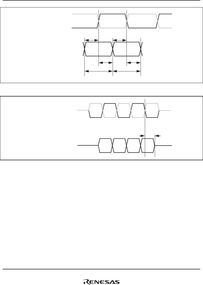
32. Electrical Characteristics
Rev.1.00 Jan. 10, 2008 Page 1596 of 1658
REJ09B0261-0100
MDQS[3:0] (solid line)
MDQS[3:0] (dotted line)
MDQ[31:0]
MDM[3:0]
t
WDS
t
WDH
t
WDS
t
WDH
t
WDIPW
t
WDIPW
Figure 32.32 MDQS and MDQ/MDM Output Waveform (Write)
MDQS[3:0] (solid line)
MDQS[3:0] (dotted line)
tHZ
HiZ HiZ
HiZ
MDQ[31:0]
Figure 32.33 MDQ High-Impedance Time from MDQS (Write)
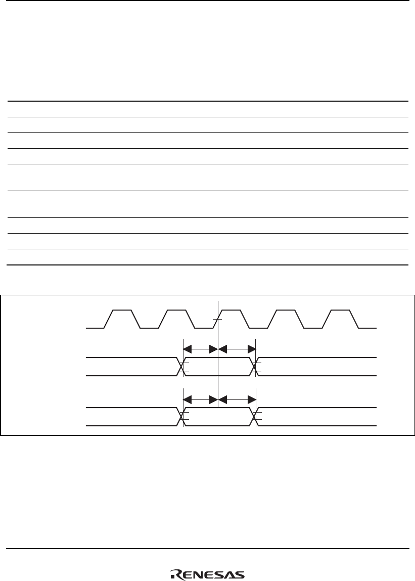
32. Electrical Characteristics
Rev.1.00 Jan. 10, 2008 Page 1597 of 1658
REJ09B0261-0100
32.3.5 INTC Module Signal Timing
Table 32.10 INTC Module Signal Timing
Conditions: VDDQ= 3.0 to 3.6 V, VDD= 1.1 V, Ta= −40 to 85°C, CL= 30 pF, PLL2 on
Item Symbol Min. Typ. Max. Unit Figure
NMI setup time tNMIS 4 — — ns 32.34
NMI hold time tNMIH 1.5 — — ns 32.34
NMI pulse width (high level) tNMIIS 5 — — tcyc* 32.35
NMI pulse width (low level) tNMIIH 5 — — tcyc* 32.35
Edge-sense IRQ pulse width (high
level)
tIRQIH 5 — — tcyc* 32.35
Edge-sense IRQ pulse width (low
level)
tIRQIL 5 — — tcyc* 32.35
IRL7 to IRL0 setup time tIRLS 4 — — ns 32.34
IRL7 to IRL0 hold time tIRLH 1.5 — — ns 32.34
IRQOUT delay time tIRQOD 1.5 — 6 ns 32.36
Note: * t
cyc is the period of one CLKOUT cycle.
CLKOUT
NMI
IRL3 to IRL0
IRL7 to IRL4
t
NMIS
t
NMIH
t
IRLS
t
IRLH
Figure 32.34 Interrupt Signal Input Timing (1)
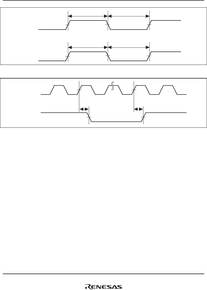
32. Electrical Characteristics
Rev.1.00 Jan. 10, 2008 Page 1598 of 1658
REJ09B0261-0100
NMI
IRQ
t
NMIIH
t
NMIIL
t
IRQIH
t
IRQIL
Figure 32.35 Interrupt Signal Input Timing (2)
CLKOUT
t
IRQOD
t
IRQOD
IRQOUT
Figure 32.36 IRQOUT Timing

32. Electrical Characteristics
Rev.1.00 Jan. 10, 2008 Page 1599 of 1658
REJ09B0261-0100
32.3.6 PCIC Module Signal Timing
Table 32.11 PCIC Signal Timing (in PCIREQ/PCIGNT Non-Port Mode) (1)
Conditions: VDDQ = 3.0 to 3.6 V, VDD = 1.1 V, Ta = –40 to 85°C, CL = 30 pF
33 MHz 66 MHz
Pin Item Symbol Min. Max. Min. Max. Unit Figure
Clock period tPCICYC 30 — 15 30 ns 32.37
Clock pulse width (high) tPCIHIGH 11 — 6 —
Clock pulse width (low) tPCIr 11 — 6 —
Clock rise time tPCIf — 4 — 1.5
PCICLK
Clock fall time tNCDAD1 — 4 — 1.5
PCIRESET Output data delay time tPCIVAL — 10 — 10 ns 32.38
Input setup time tPCISU 3 — 3 — ns 32.39 IDSEL
Input hold time tPCIH 1.5 — 1.5 —
Output data delay time tPCIVAL 2 10 2 6 ns 32.38
Tri-state drive delay time tPCION 2 10 2 6
Tri-state Hi-Z delay time tPCIOFF 2 12 2 6
Input setup time tPCISU 3 — 3 — 32.39
AD31 to AD0,
C/BE3 to C/BE0,
PCIFRAME,
PAR, IRDY,
TRDY, STOP,
LOCK, PERR,
DEVSEL, Input hold time tPCIH 1.5 — 1.5 —
Output data delay time tPCIVAL 2 10 2 6 ns 32.38
Input setup time tPCISU 3 — 3 — 32.39
REQ0/REQOUT,
GNT0/GNTIN
REQ1, REQ2,
REQ3, GNT1,
GNT2, GNT3
Input hold time tPCIH 1.5 — 1.5 —
Tri-state drive delay time tPCION — 10 — 10 ns 32.38
Tri-state Hi-Z delay time tPCIOFF — 12 — 12
SERR, INTA,
INTB, INTC,
INTD Input setup time tPCISU 3 — 3 — 32.39
Input hold time tPCIH 1.5 — 1.5 —
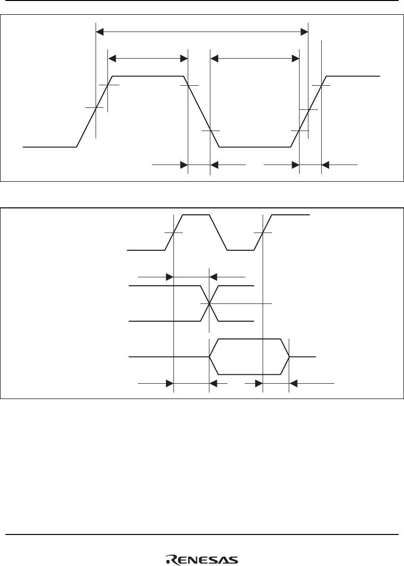
32. Electrical Characteristics
Rev.1.00 Jan. 10, 2008 Page 1600 of 1658
REJ09B0261-0100
0.5V
DDQ
0.5V
DDQ
t
PCICYC
t
PCIHIGH
t
PCILOW
t
PCIf
t
PCIr
V
L
V
L
V
H
V
H
V
H
Figure 32.37 PCI Clock Input Timing
t
PCIVAL
0.4V
DDQ
0.4V
DDQ
PCICLK
Tri-state output
Output delay
t
PCION
t
PCIOFF
Figure 32.38 PCI Output Signal Timing
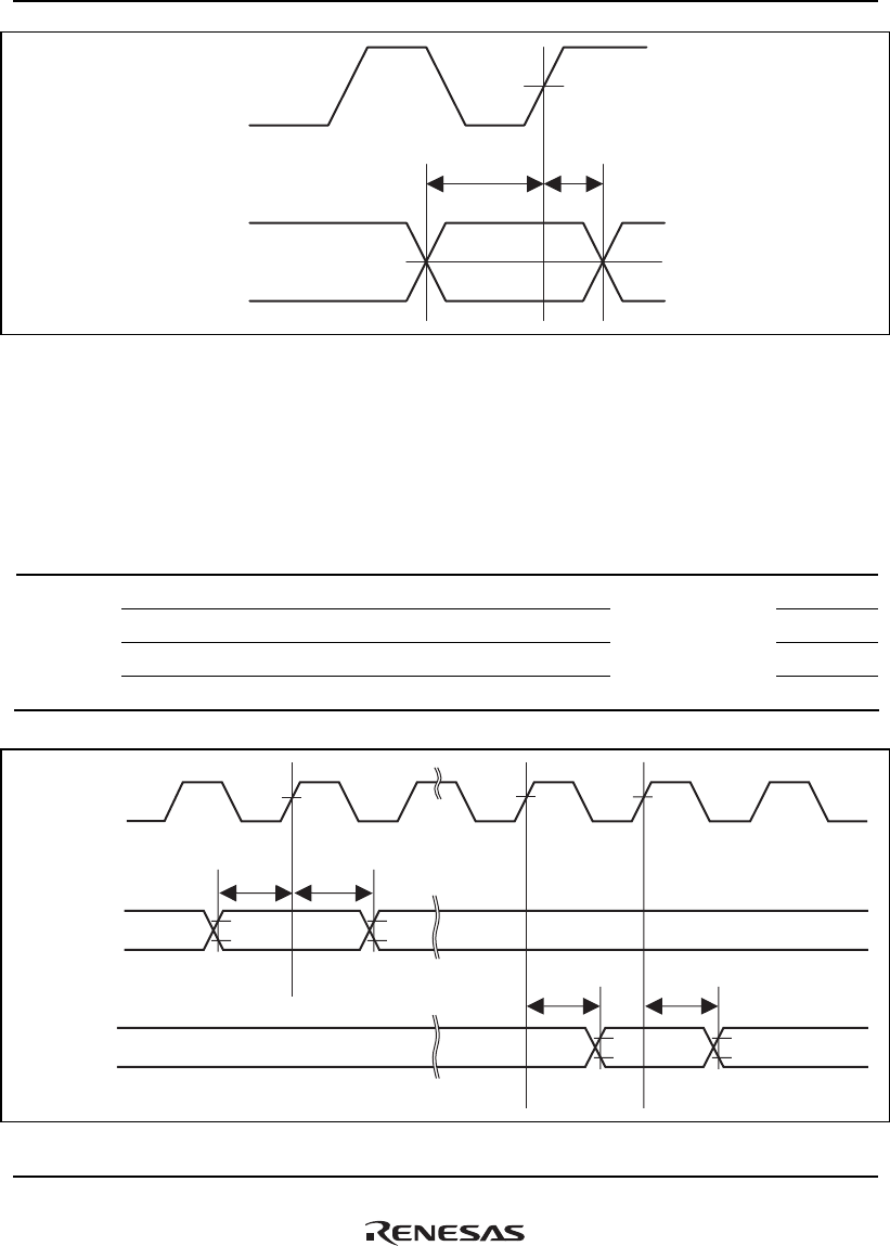
32. Electrical Characteristics
Rev.1.00 Jan. 10, 2008 Page 1601 of 1658
REJ09B0261-0100
t
PCISU
0.4V
DDQ
PCICLK
Input
0.4V
DDQ
t
PCIH
Figure 32.39 PCI Input Signal Timing
32.3.7 DMAC Module Signal Timing
Table 32.12 DMAC Module Signal Timing
Conditions: VDDQ= 3.0 to 3.6 V, VDD= 1.5 V, Ta= −40 to 85°C, CL= 30 pF, PLL2 on
Module Item Symbol Min. Max. Unit Figure Remarks
DMAC DREQ setup time tDRQS 2.5 — ns 32.40
DREQ hold time tDRQH 1.5 —
DRAK delay time tDRAKD 1.5 6
DACK delay time tDAKD 1.5 6
t
DRQS
CLKOUT
DRAK
DREQ
t
DRQH
t
DRAKD
t
DRAKD
Figure 32.40 DREQ/DRAK Signal Timing
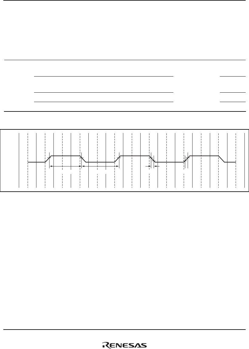
32. Electrical Characteristics
Rev.1.00 Jan. 10, 2008 Page 1602 of 1658
REJ09B0261-0100
32.3.8 TMU Module Signal Timing
Table 32.13 TMU Module Signal Timing
Conditions: VDDQ= 3.0 to 3.6 V, VDD= 1.1 V, Ta= −40 to 85°C, CL= 30 pF, PLL2 on
Module Item Symbol Min. Max. Unit Figure Remarks
TMU Timer clock pulse width
(high)
tTCLKWH 4 — tPcyc 32.41
Timer clock pulse width
(low)
tTCLKWL 4 —
Timer clock rise time tTCLKr — 0.8
Timer clock fall time tTCLKf — 0.8
Note: tPcyc is the period of one peripheral clock (Pck) cycle.
t
TCLKWH
t
TCLKWL
t
TCLKf
t
TCLKr
TCLK
Figure 32.41 TCLK Input Timing
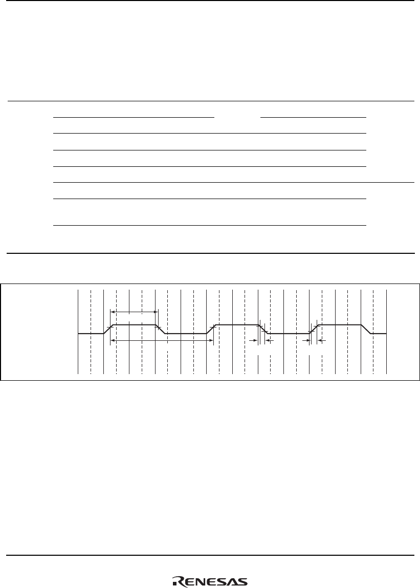
32. Electrical Characteristics
Rev.1.00 Jan. 10, 2008 Page 1603 of 1658
REJ09B0261-0100
32.3.9 SCIF Module Signal Timing
Table 32.14 SCIF Module Signal Timing
Conditions: VDDQ= 3.0 to 3.6 V, VDD= 1.1 V, Ta= −40 to 85°C, CL= 30 pF, PLL2 on
Module Item Symbol Min. Max. Unit Figure
SCIFn Input clock cycle (asynchronous) tScyc 4 — tPcyc
Input clock cycle (clock synchronous) 10 — tPcyc
Input clock pulse width tSCKW 0.4 0.6 tScyc
Input clock rise time tSCKr — 0.8 tPcyc
Input clock fall time tSCKf — 0.8 tPcyc
32.42
Transfer data delay time tTXD — 6 tPcyc 32.43
Receive data setup time
(clock synchronous)
tRXS 16 — ns
Receive data hold time
(clock synchronous)
tRXH 16 — ns
Note: tpcyc means one cycle time of the peripheral clock (Pck).
t
SCKW
t
Scyc
t
SCKf
t
SCKr
SCIFn_CLK
Figure 32.42 SCIFn_CLK Input Clock Timing
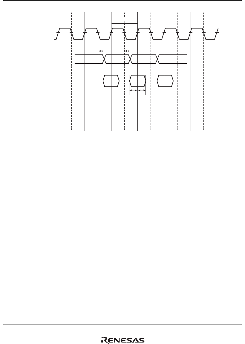
32. Electrical Characteristics
Rev.1.00 Jan. 10, 2008 Page 1604 of 1658
REJ09B0261-0100
t
Scyc
t
TXD
t
RXS
t
RXH
SCIFn_CLK
SCIFn_TXD
SCIFn_RXD
t
TXD
Figure 32.43 Clock Timing in SCIF I/O Synchronous Mode
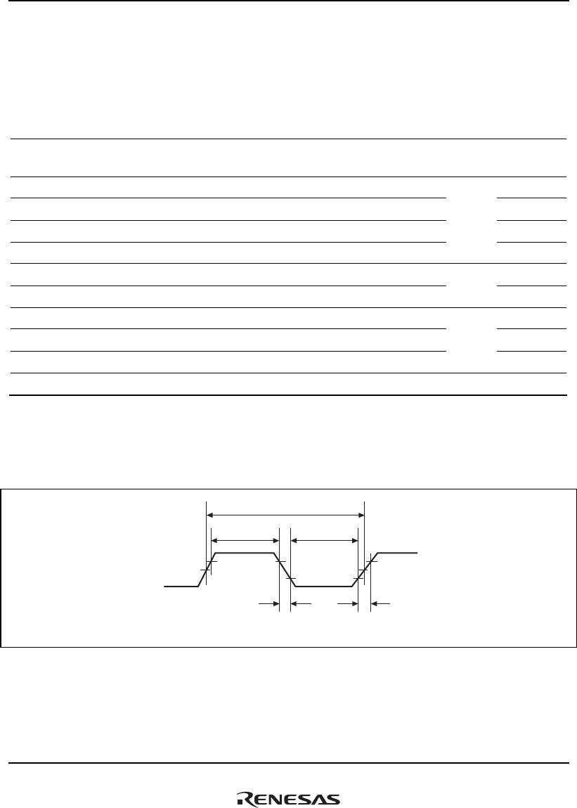
32. Electrical Characteristics
Rev.1.00 Jan. 10, 2008 Page 1605 of 1658
REJ09B0261-0100
32.3.10 H-UDI Module Signal Timing
Table 32.15 H-UDI Module Signal Timing
Conditions: VDDQ= 3.0 to 3.6 V, VDD= 1.1 V, Ta= −40 to 85°C, CL= 30 pF, PLL2 on
Item Symbol Min. Max. Unit Figure Remarks
Input clock cycle tTCKcyc 50 — ns 32.44,
32.46
Input clock pulse width (high) tTCKH 15 — ns 32.44
Input clock pulse width (low) tTCKL 15 — ns
Input clock rise time tTCKr — 10 ns
Input clock fall time tTCKf — 10 ns
ASEBRK setup time tASEBRKS 10 — tcyc 32.45
ASEBRK hold time tASEBRKH 1 — ms
TDI/TMS setup time tTDIS 15 — ns 32.46
TDI/TMS hold time tTDIH 15 — ns
TDO data delay time tTDO 0 12 ns
ASE-PINBRK pulse width tPINBRK 2 — tPcyc 32.47
Notes: 1. During a boundary scan, tTCKcyc is the period corresponding to a frequency of 10 MHz, i.e.
0.1 μs.
2. tcyc is the period of one CKIO clock cycle.
3. tPcyc is the period of one peripheral clock (Pck) cycle.
t
TCKH
t
TCKf
t
TCKr
t
TCKL
t
TCKcyc
V
IH
V
IH
V
IH
1/2V
DDQ
1/2V
DDQ
V
IL
V
IL
Note: When the clock is input from the TCK pin.
Figure 32.44 TCK Input Timing
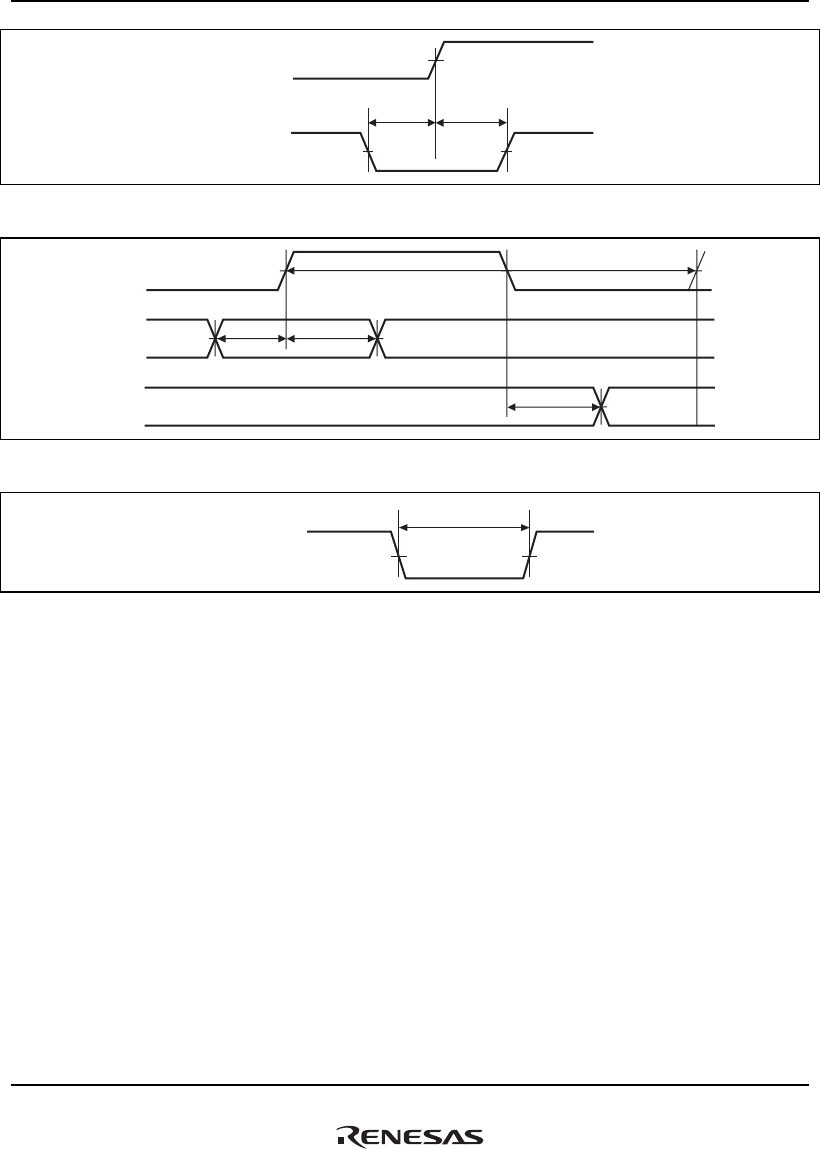
32. Electrical Characteristics
Rev.1.00 Jan. 10, 2008 Page 1606 of 1658
REJ09B0261-0100
ASEBRK
BRKACK
RESET
t
ASEBRKH
t
ASEBRKS
Figure 32.45 RESET Hold Timing
TDI
TMS
TCK
TDO
t
TCKcyc
t
TDO
t
TDIH
t
TDIS
Figure 32.46 H-UDI Data Transfer Timing
t
PINBRK
ASEBRK
Figure 32.47 Pin Break Timing
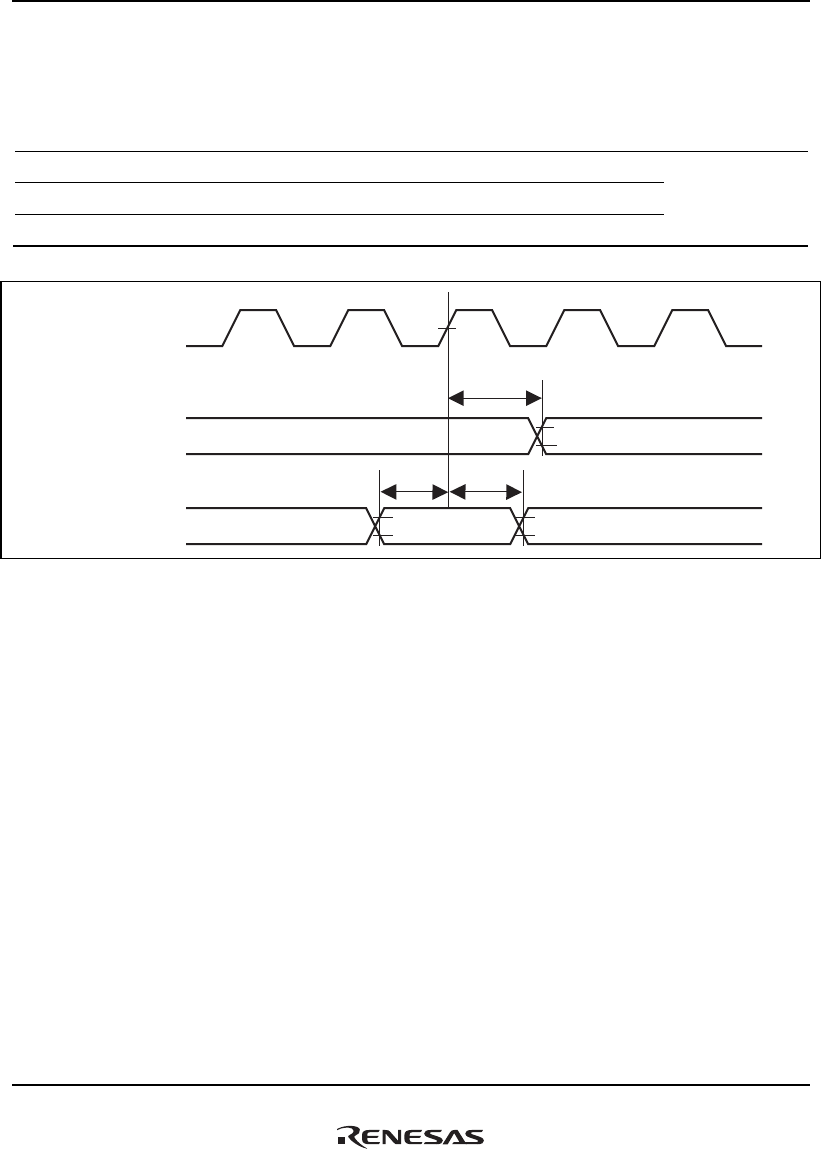
32. Electrical Characteristics
Rev.1.00 Jan. 10, 2008 Page 1607 of 1658
REJ09B0261-0100
32.3.11 GPIO Signal Timing
Table 32.16 GPIO Signal Timing
Item Symbol Min. Max. Unit Figure
GPIO output delay time tIOPD — 8 ns 32.48
GPIO input setup time tIOPS 3.5 — ns
GPIO input hold time tIOPH 1.5 — ns
t
IOPD
t
IOPS
t
IOPH
CLKOUT
GPIO[n] (OUTPUT)
GPIO[n] (INPUT)
Figure 32.48 GPIO Signal Timing
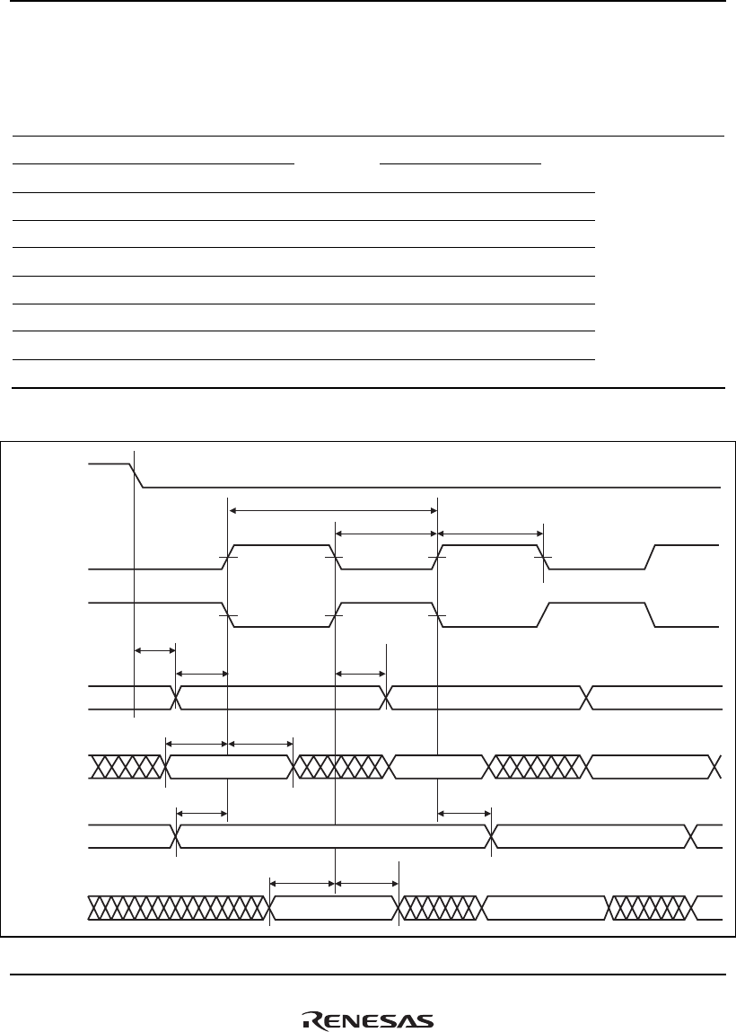
32. Electrical Characteristics
Rev.1.00 Jan. 10, 2008 Page 1608 of 1658
REJ09B0261-0100
32.3.12 HSPI Module Signal Timing
Table 32.17 HSPI Module Signal Timing
Item Symbol Min. Max. Unit Figure
HSPI clock frequency (master) TSPICYC — Pck/8 MHz 32.49
HSPI clock frequency (slave) Pck/12
HSPI clock high level width tSPIHW 60 — ns
HSPI clock low level width tSPILW 60 — ns
HSPI_TX setup time tSUSPITX — 20 ns
HSPI_TX delay time tDSPITX — 20 ns
HSPI_RX setup time tSUSPIRX 20 — ns
HSPI_RX hold time tHLSPIRX 20 — ns
HSPI_CS lead time tcCSLEAD 100 — ns
Note: Pck is the frequency of the peripheral clock.
HSPI_CS
t
SPICYC
t
CSLEAD
t
SUSPITX
t
SUSPIRX
t
SUSPIRX
t
HLSPIRX
t
SUSPITX
t
DSPITX
t
HLSPIRX
t
DSPITX
t
SPILW
t
SPIHW
(CLKP = 0)
HSPI_CLK
(CLKP = 1)
HSPI_CLK
(LMSB = 0)
HSPI_TX
(LMSB = 1)
HSPI_TX
HSPI_RX
HSPI_RX
MSB-1MSB
MSB
MSB
MSB MSB-1
MSB-1
MSB-1 MSB-2
Figure 32.49 HSPI Data Output/Input Timing
32. Electrical Characteristics
Rev.1.00 Jan. 10, 2008 Page 1609 of 1658
REJ09B0261-0100
32.3.13 SIOF Module Signal Timing
Table 32.18 SIOF Module Signal Timing
Item Symbol Min. Max. Unit Figure
SIOF_MCLK clock input cycle time tMCYC t
pcyc — ns 32.50
SIOF_MCLK input high level width tMWH 0.4 × tMCYC — ns
SIOF_MCLK input low level width tMWL 0.4 × tMCYC — ns
SIOF_SCK clock cycle time tSICYC t
pcyc — ns 32.51 to 32.55
SIOF_SCK output high level width tSWHO 0.4 × tSICYC — ns 32.51 to 32.54
SIOF_SCK output low level width tSWLO 0.4 × tSICYC — ns
SIOF_SYNC output delay time tFSD — 10 ns
SIOF_SCK input high level width tSWHI 0.4 × tSICYC — ns 32.55
SIOF_SCK input low level width tSWLI 0.4 × tSICYC — ns
SIOF_SYNC input setup time tFSS 10 — ns
SIOF_SYNC input hold time tFSH 10 — ns
SIOF_TXD output delay time tSTDD — 10 ns 32.51 to 32.55
SIOF_RXD input setup time tSRDS 10 — ns
SIOF_RXD input hold time TSRDH 10 — ns
t
MCYC
SIOF_MCLK
t
MWH
t
MWL
Figure 32.50 SIOF_MCLK Input Timing
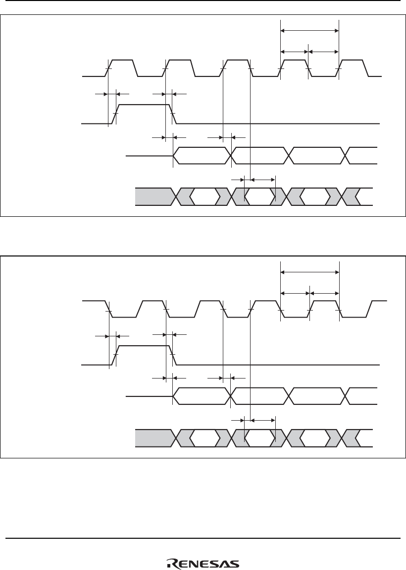
32. Electrical Characteristics
Rev.1.00 Jan. 10, 2008 Page 1610 of 1658
REJ09B0261-0100
SIOF_SCK (Output)
SIOF_SYNC (Output)
SIOF_TXD
SIOF_RXD
tFSD tFSD
tSICYC
tSWHO tSWLO
tSTDD tSTDD
tSRDS tSRDH
Figure 32.51 SIOF Transmission/Reception Timing
(Master Mode 1, Sampling on Falling Edges)
SIOF_SCK (Output)
SIOF_SYNC (Output)
SIOF_TXD
SIOF_RXD
tSICYC
tSWHO
tSWLO
tFSD tFSD
tSTDD tSTDD
tSRDS tSRDH
Figure 32.52 SIOF Transmission/Reception Timing
(Master Mode 1, Sampling on Rising Edges)
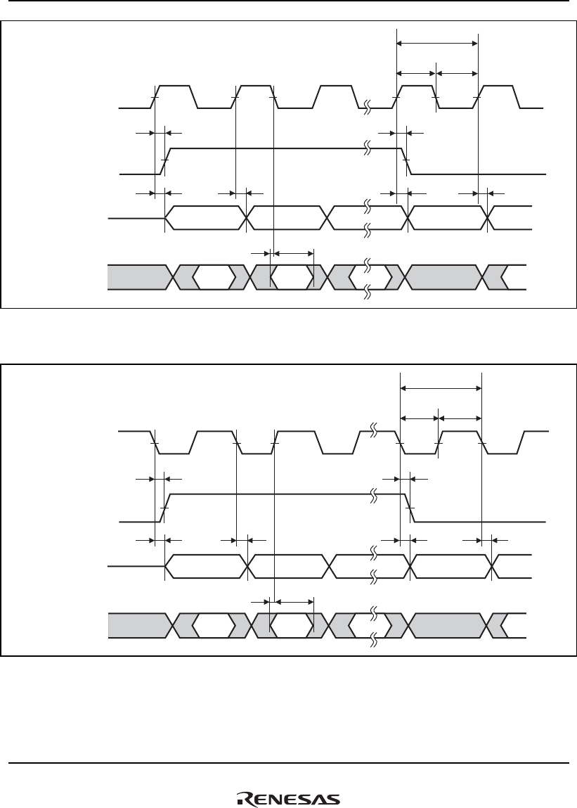
32. Electrical Characteristics
Rev.1.00 Jan. 10, 2008 Page 1611 of 1658
REJ09B0261-0100
SIOF_SCK (Output)
SIOF_SYNC (Output)
SIOF_TXD
SIOF_RXD
t
FSD
t
FSD
t
SICYC
t
SWHO
t
SWLO
t
STDD
t
STDD
t
STDD
t
STDD
t
SRDS
t
SRDH
Figure 32.53 SIOF Transmission/Reception Timing
(Master Mode 2, Sampling on Falling Edges)
SIOF_SCK (Output)
SIOF_SYNC (Output)
SIOF_TXD
SIOF_RXD
tSICYC
tSWLO
tFSD
tSTDD
tSTDD
tSRDS tSRDH
tSTDD
tFSD
tSTDD
tSWHO
Figure 32.54 SIOF Transmission/Reception Timing
(Master Mode 2, Sampling on Rising Edges)
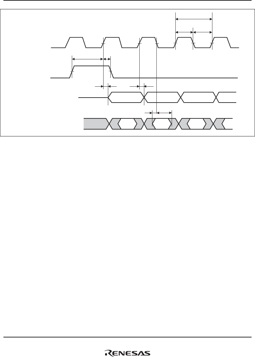
32. Electrical Characteristics
Rev.1.00 Jan. 10, 2008 Page 1612 of 1658
REJ09B0261-0100
SIOF_SCK (Output)
SIOF_SYNC (Output)
SIOF_TXD
SIOF_RXD
t
SICYC
t
SWHI
t
SWLI
t
FSH
t
FSS
t
STDD
t
STDD
t
SRDS
t
SRDH
Figure 32.55 SIOF Transmission/Reception Timing (Slave Mode 1, Slave Mode 2)
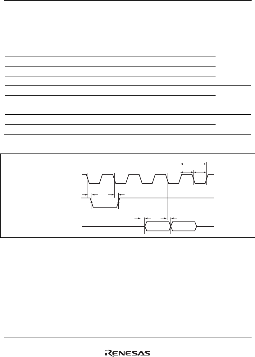
32. Electrical Characteristics
Rev.1.00 Jan. 10, 2008 Page 1613 of 1658
REJ09B0261-0100
32.3.14 MMCIF Module Signal Timing
Table 32.19 MMCIF Module Signal Timing
Item Symbol Min. Max. Unit Figure
MMCCLK clock cycle time tMMcyc 50 — ns
MMCCLK clock high level width tMMWH 0.4 × tMmcyc — ns
MMCCLK clock low level width tMMWL 0.4 × tMMcyc — ns
MMCCMD output data delay time tMMTCD — 10 ns
32.56
MMCCMD input data hold time tMMRCS 10 — ns
MMCCMD input data setup time tMMRCH 10 — ns
32.57, 32.58
MMCD output data delay time tMMTDD — 10 ns 32.56
MMCD input data setup time tMMRDS 10 — ns 32.57, 32.58
MMCD input data hold time tMMRDH 10 — ns
Note: tMmcyc is the period of one MMCCLK cycle.
tMMcyc
tMMWH
tMMTDD tMMTDD
tMMTCD tMMTCD
tMMWL
MMCLK
MMCCMD (Output)
MMCDAT (Output)
Figure 32.56 MMCIF Transmission Timing
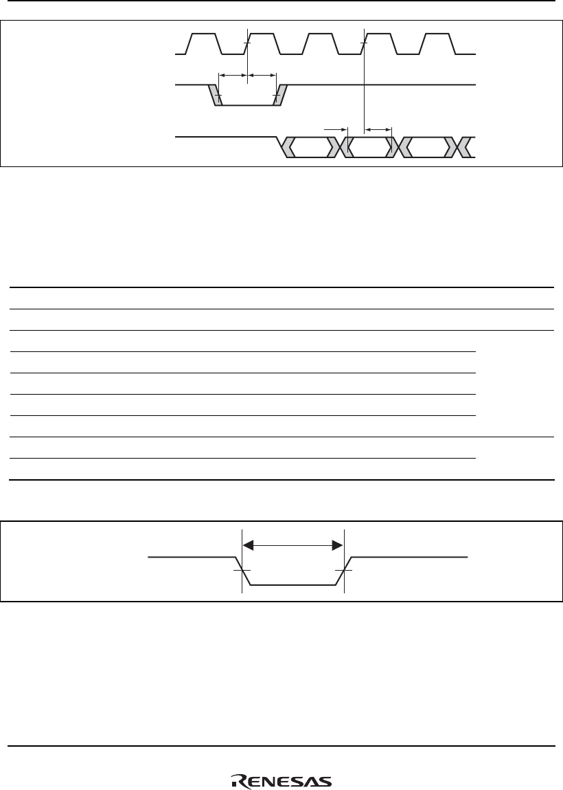
32. Electrical Characteristics
Rev.1.00 Jan. 10, 2008 Page 1614 of 1658
REJ09B0261-0100
t
MMRCS
t
MMRCH
MMCCLK
MMCCMD (Input)
MMCDAT (Input)
t
MMRDS
t
MMRDH
Figure 32.57 MMCIF Reception Timing (Sampling on Rising Edges)
32.3.15 HAC Interface Module Signal Timing
Table 32.20 HAC Interface Module Signal Timing
Item Symbol Min. Max. Unit Figure
HAC_RES active low pulse width tRST_LOW 1000 — ns 32.58
HAC_SYNC active pulse width tSYN_HIGH 1000 — ns 32.59
HAC_SYNC delay time 1 tSYNCD1 — 15 ns
HAC_SYNC delay time 2 tSYNCD2 — 15 ns
HAC_SDOUT delay time tSDOUTD — 15 ns
HAC_SDIN setup time tSDIN0S 10 — ns
HAC_SDIN hold time tSDIN0H 10 — ns
32.61
HAC_BITCLK input high level width tICL0_HIGH t
Pcyc/2 — ns 32.60
HAC_BITCLK input low level width tICL0_LOW t
Pcyc/2 — ns
Note: tPcyc is the period of one peripheral clock (Pck) cycle.
HAC_RES
t
RST_LOW
Figure 32.58 HAC Cold Reset Timing
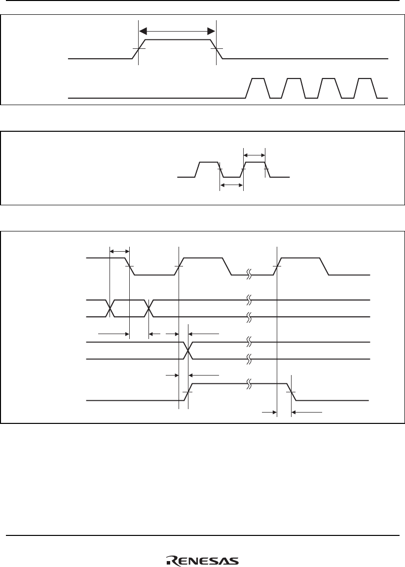
32. Electrical Characteristics
Rev.1.00 Jan. 10, 2008 Page 1615 of 1658
REJ09B0261-0100
HACn_SYNC
HACn_BITCLK
t
SYN_HIGH
Figure 32.59 HAC Warm Reset Timing
HACn_BITCLK
t
ICL_HIGH
t
ICL_LOW
Figure 32.60 HAC Clock Input Timing
HACn_BITCLK
HACn_SDIN
HACn_SDOUT
t
SDNHD
t
SDNSU
t
SDCUTD
t
SYNCD1
t
SYNCD2
HACn_SYNC
Figure 32.61 HAC Interface Module Signal Timing
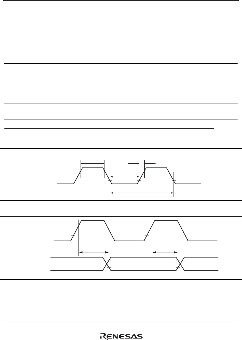
32. Electrical Characteristics
Rev.1.00 Jan. 10, 2008 Page 1616 of 1658
REJ09B0261-0100
32.3.16 SSI Interface Module Signal Timing
Table 32.21 SSI Interface Module Signal Timing
Item Symbol Min. Max. Unit Remarks Figure
Output cycle time tOSCK 40 710 ns Output
Input cycle time tISCK 80 3300 ns Input
Input high level width/input low level
width
tIHC/tILC 30 ns Input 32.62
Output high level width/output low level
width
TOHC/tOLC 13 ns Output
SCK output rise time tRC — 60 ns Output
SDATA output delay time tDTR — 50 ns Transmit 32.63,
32.64
SDATA/WS input setup time tSR 10 — ns Receive
SDATA/WS input hold time tHTR 10 — ns Receive
32.65,
32.66
t
OHC
t
IHC
t
RC
V
IH
V
OH
V
IH
V
OH
V
IL
V
OH
t
OLC
t
ISCK
t
OSCK
t
ILC
SSIn_SCK
V
IH
V
OH
V
IH
V
OH
V
IL
V
OH
Figure 32.62 SSI Clock Input/Output Timing
t
DTR
t
HTR
SSIn_SCKn
SSIn_WS
SSIn_SDATA
Figure 32.63 SSI Transmission Timing (1)
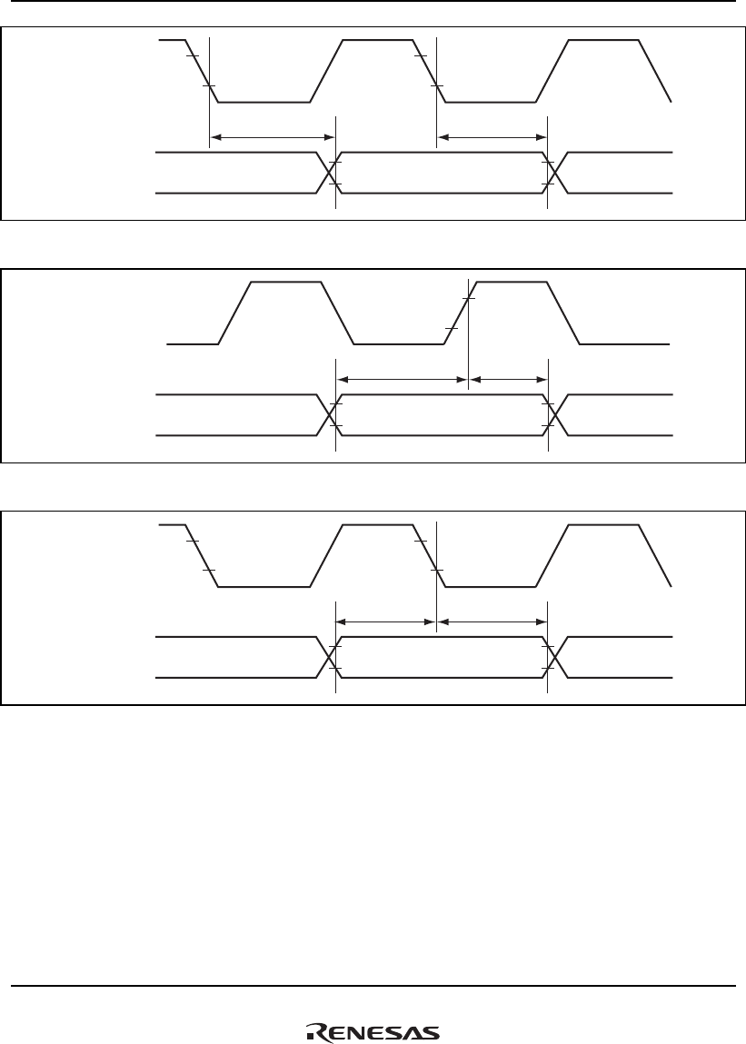
32. Electrical Characteristics
Rev.1.00 Jan. 10, 2008 Page 1617 of 1658
REJ09B0261-0100
t
DTR
t
HTR
SSIn_SCK
SSIn_WS
SSIn_SDATA
Figure 32.64 SSI Transmission Timing (2)
t
SR
t
HTR
SSIn_SCK
SSIn_WS
SSIn_SDATA
Figure 32.65 SSI Reception Timing (1)
t
HTR
t
SR
SSIn_SCK
SSIn_WS
SSIn_SDATA
Figure 32.66 SSI Reception Timing (2)

32. Electrical Characteristics
Rev.1.00 Jan. 10, 2008 Page 1618 of 1658
REJ09B0261-0100
32.3.17 FLCTL Module Signal Timing
Table 32.22 NAND-Type Flash Memory Interface Timing
Item Symbol Min. Max. Unit Figure
Command issue setup time tNCDS 2 × tfcyc −10 — ns
Command issue hold time tNCDH 1.5 × tfcyc −10 — ns
32.67, 32.71
Data output setup time tNDOS 0.5 tfcyc −10 — ns
Data output hold time tNDOH 0.5 tfcyc −10 — ns
32.67, 32.68,
32.70, 32.71
Command to address transition time 1 tNCDAD1 1.5 × tfcyc −10 — ns 32.67, 32.68
Command to address transition time 2 tNCDAD2 2 × tfcyc −10 — ns 32.68
FWE cycle time tNWC t
fcyc −5 — ns 32.68, 32.70
FWE low pulse width tNWP 0.5 tfcyc −5 — ns 32.67, 32.68,
32.70, 32.71
FWE high pulse width tNWH 0.5 tfcyc −5 — ns 32.68, 32.70
Address to ready/busy transition time tNADRB — 32 × tpcyc ns 32.68, 32.69
Ready/busy to data read transition
time 1
tNRBDR1 1.5 × tfcyc — ns
Ready/busy to data read transition
time 2
tNRBDR2 32 × tpcyc — ns
FSC cycle time tNSCC t
fcyc — ns
FSC high pulse width tNSPH 0.5 × tfcyc −5 — ns
32.69
FSC low pulse width tNSP 0.5 × tfcyc −5 — ns
Read data setup time tNRDS 24 — ns
Read data hold time tNRDH 5 — ns
32.69, 32.71
Data write setup time tNDWS 32 × tpcyc −10 — ns 32.70
Command to status read transition
time
tNCDSR 4 × tfcyc −10 — ns 32.71
Command output off to status read
transition time
tNCDFSR 3.5 × tfcyc — ns
Status read setup time tNSTS 2.5 × tfcyc −10 ns
Notes: 1. tpcyc is the period of one peripheral clock (Pck) cycle.
2. tfcyc is the period of one FLCTL clock (Fck) cycle.
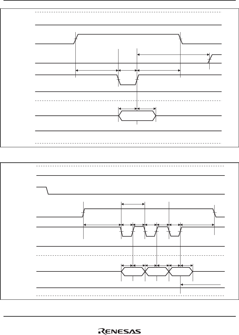
32. Electrical Characteristics
Rev.1.00 Jan. 10, 2008 Page 1619 of 1658
REJ09B0261-0100
FCE (Low)
(High)
(High)
FCLE
FR/B
FD7 to FD0
FRE
FWE
FALE
Command
t
NCDAD1
t
NCDS
t
NWP
t
NDOS
t
NDOH
t
NCDH
Figure 32.67 Command Issue Timing of NAND-Type Flash Memory
FD7 to FD0
FCE (Low)
(High)
(High)
FCLE
FALE
FWE
FRE
FR/B
tNWC
tNCDAD2
tNDOS tNDOH tNDOH
tNDOS tNDOH
tNDOS
tNCDAD1
tNADRB
tNWP tNWH tNWH
tNWP tNWP
Address Address Address
Figure 32.68 Address Issue Timing of NAND-Type Flash Memory
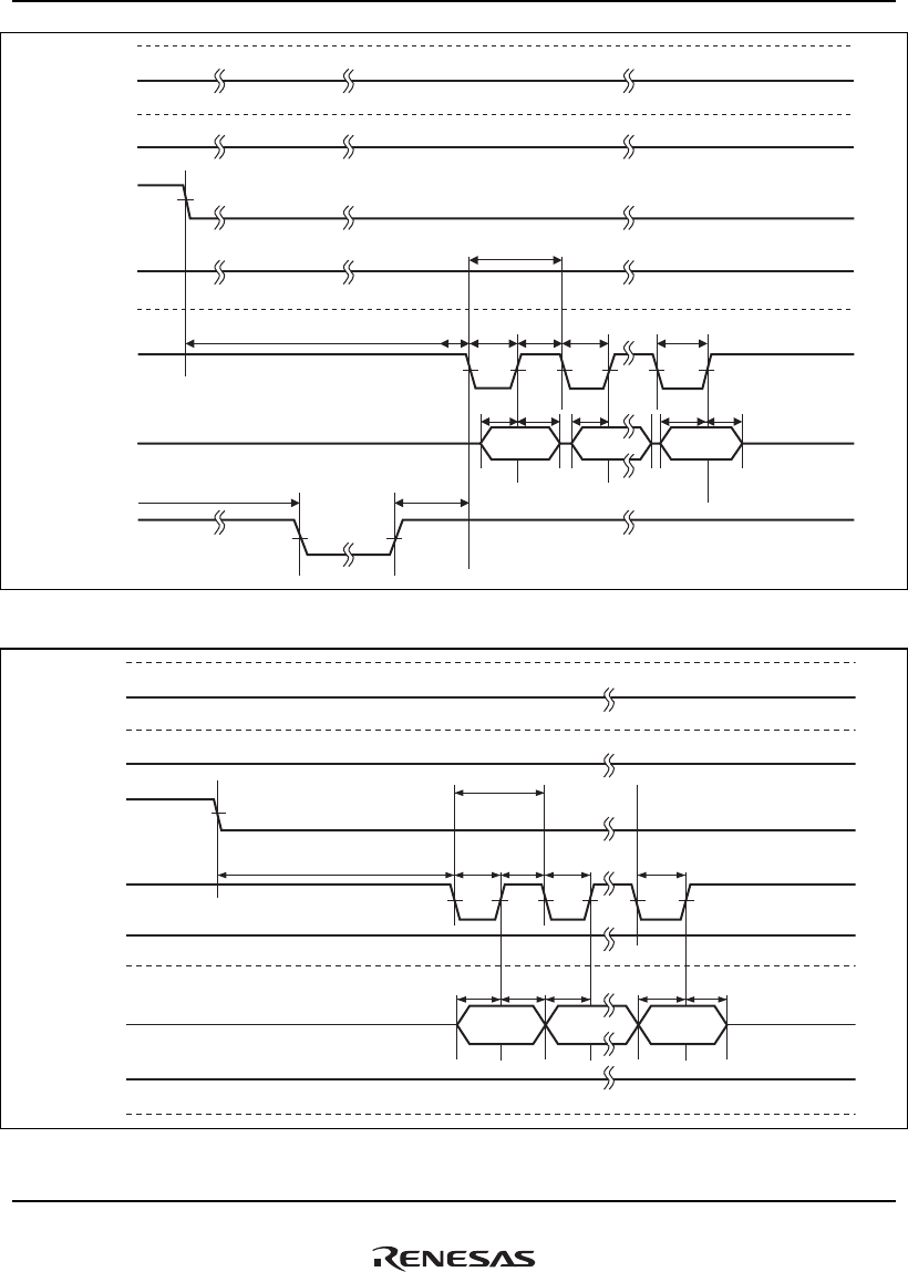
32. Electrical Characteristics
Rev.1.00 Jan. 10, 2008 Page 1620 of 1658
REJ09B0261-0100
FD7 to FD0
(Low)
(Low)
(High)
FCE
FCLE
FALE
FWE
FRE
FR/B
t
NRBDR2
t
NADRB
t
NRBDR1
t
NSP
t
NRDS
t
NRDS
t
NRDH
t
NRDS
t
NRDH
t
NSCC
t
NSPH
t
NSP
t
NSP
Data Data
Figure 32.69 Data Read Timing of NAND-Type Flash Memory
FD7 to FD0
FCE
FCLE
FALE
FRE
FR/B
FWE
(Low)
(Low)
(High)
(High)
tNDWS
t
NWP
t
NWC
t
NDOS
t
NDOH
t
NDOS
t
NDOH
t
NDOS
t
NWH
t
NWP
t
NWP
Data Data
Figure 32.70 Data Write Timing of NAND-Type Flash Memory
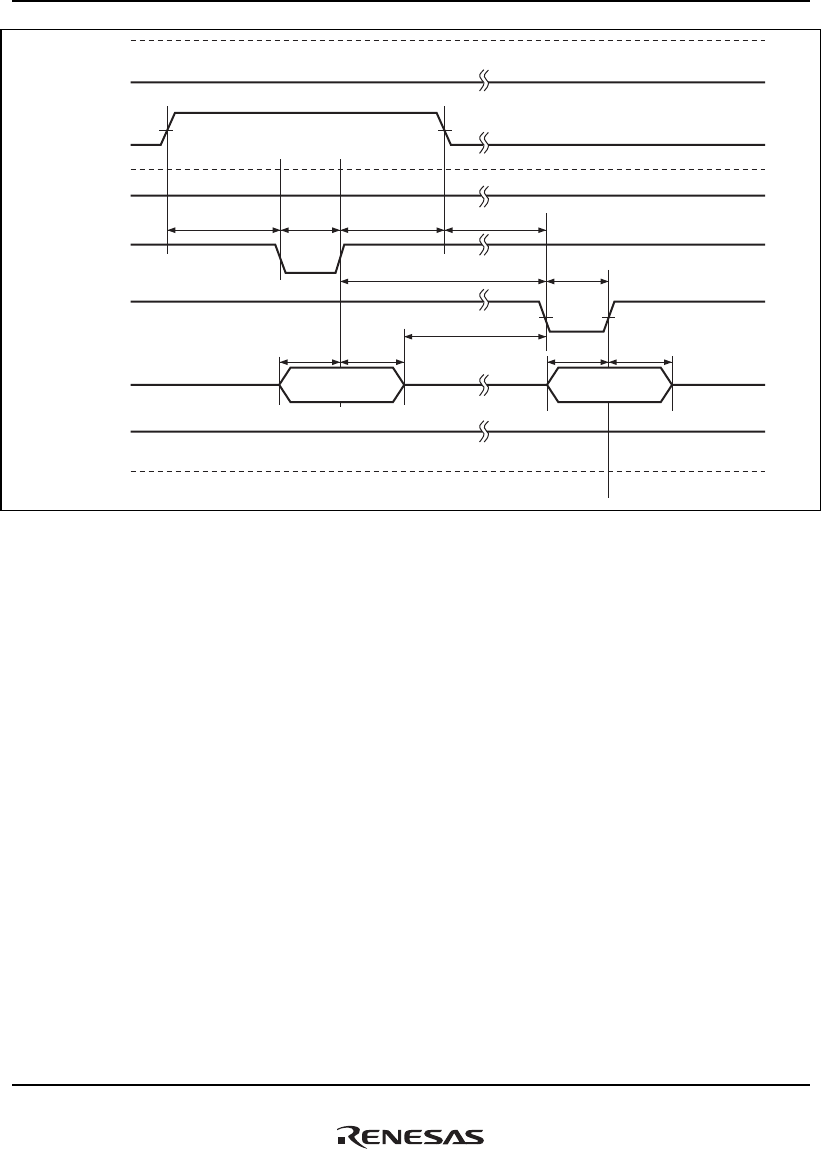
32. Electrical Characteristics
Rev.1.00 Jan. 10, 2008 Page 1621 of 1658
REJ09B0261-0100
FCE
FCLE
FALE
FRE
FR/B
FD7 to FD0
FWE
(Low)
(Low)
(High)
t
NCDS
t
NDOS
t
NRDS
t
NRDH
t
NDOH
t
NWP
t
NCDH
t
NSTS
t
NCDSR
t
NCDFSR
t
NSP
Command Status
Figure 32.71 Status Read Timing of NAND-Type Flash Memory

32. Electrical Characteristics
Rev.1.00 Jan. 10, 2008 Page 1622 of 1658
REJ09B0261-0100
32.3.18 Display Unit Signal Timing
Table 32.23 PCICLK/DCLKIN Signal Timing
Conditions: VDDQ = 3.3 V ±0.3 V, Ta = -40°C to + 85°C, GND = VSSQ = 0 V
Item Symbol Min. Typ. Max. Unit Figure
PCICLK/DCLKIN cycle time tDICYC 20 — — ns 32.72
PCICLK/DCLKIN high level width tDCKIH 8 — — ns
PCICLK/DCLKIN low level width tDCKIL 8 — — ns
Table 32.24 Display Timing
Conditions: VDDQ = 3.3 V ±0.3 V, Ta = –40°C to +85°C, GND = VSSQ = 0 V
Item Symbol Min. Typ. Max. Unit Figures
Display input control
signal setup time
tDS 5 — — ns
Display input control
signal hold time
tDH 3 — — ns
Figure 32.73
(with respect to
PCICLK/
DCLKIN)
DEVSEL/DCLKOUT
output cycle time
tDCYC 20 — — ns
DEVSEL/DCLKOUT
output high level width
tDCKH 6 — — ns
Delay time of display
output control signal
output
tDD -2 — 8 ns
Display digital data output
delay time
tDD -2 — 8 ns
Figure 32.74
(with respect to
DEVSEL/
DCLKOUT)
IRDY/HSYNC input low
level width
tEXHLW 4 × tDCYC — — ns Figure 32.75
IRDY/HSYNC input high
level width
tEXHHW 4 × tDCYC — — ns
PCIFRAME/VSYNC input
low level width
tEXVLW 3 × HC — — tDCYC
LOCK/ODDF setup time 1 tOD1 (ys + yw) × HC — — tDCYC
LOCK/ODDF setup time 2 tOD2 1 × HC — — tDCYC
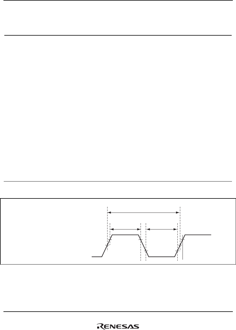
32. Electrical Characteristics
Rev.1.00 Jan. 10, 2008 Page 1623 of 1658
REJ09B0261-0100
Table 32.25 Classification of Pins
Pin Classification
Display Input Control
Signal*1
Display Output
Control Signal*2
Digital Data for
Display*3
Pin Name PCIFRAME/VSYNC
IRDY/HSYNC
LOCK/ODDF
PCIFRAME/VSYNC
IRDY/HSYNC
LOCK/ODDF
TRDY/DISP
STOP/CDE
D32/AD0/DR0
D33/AD1/DR1
D34/AD2/DR2
D35/AD3/DR3
D36/AD4/DR4
D37/AD5/DR5
D38/AD6/DG0
D39/AD7/DG1
D40/AD8/DG2
D41/AD9/DG3
D42/AD10/DG4
D43/AD11/DG5
D44/AD12/DB0
D45/AD13/DB1
D46/AD14/DB2
D47/AD15/DB3
D48/AD16/DB4
D49/AD17/DB5
Note: *1, *2, and *3 correspond to the numbers with asterisk in figures 32.73 and 32.74.
tDICYC
tDCKIH
VIH
VIL VIL
VIH VIH
1/2VDDQ
1/2VDDQ
tDCKIL
PCICLK/DCLKIN
(Input)
Figure 32.72 PCICLK/DCLKIN Clock Input Timing
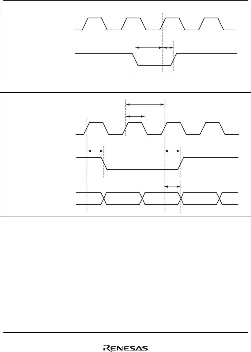
32. Electrical Characteristics
Rev.1.00 Jan. 10, 2008 Page 1624 of 1658
REJ09B0261-0100
t
DS
t
DH
PCICLK/DCLKIN
(Input)
Display input control signal*
1
(Input)
Figure 32.73 Display Timing (with Respect to PCICLK/DCLKIN)
Display output control signal*2
(Output)
Digital data for display*3
(Output)
tDD
tDCKH
tDCYC
tDD
tDD
DEVSEL/DCLKOUT
(Output)
Figure 32.74 Display Timing (with Respect to DEVSEL/DCLKOUT)
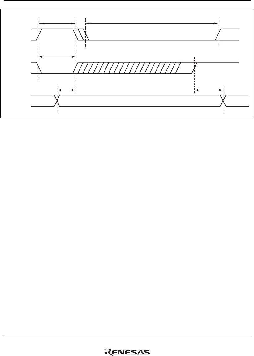
32. Electrical Characteristics
Rev.1.00 Jan. 10, 2008 Page 1625 of 1658
REJ09B0261-0100
tEXHLW
tEXHHW
tEXVHW
tOD1 tOD2
IRDY/HSYNC
(Input)
IRDY/HSYNC
(Input)
LOCK/ODDF
(Input)
Figure 32.75 Display Timing in TV Synchronous Mode
32.4 AC Characteristic Test Conditions
The AC characteristic test conditions are as follows.
DDR pin only
• Input/output signal reference level
MDQS: /MDQS cross point
MCK: /MCK cross point
Other than above: VDDQ-DDR/2
• Input pulse level: VSSQ to VDDQ-DDR
• Input rise/fall time: 0.25 ns
Other pins
• Input/output signal reference level: VDDQ/2
• Input pulse level: VSSQ to VDDQ
• Input rise/fall time: 1 ns
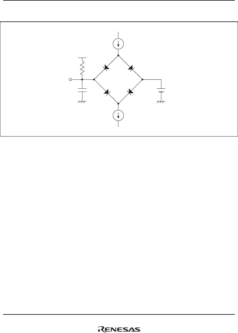
32. Electrical Characteristics
Rev.1.00 Jan. 10, 2008 Page 1626 of 1658
REJ09B0261-0100
The following figure shows the output load circuit.
I
OL
I
OH
C
L
R
T
Reference level
LSI output pin DUT output
Figure 32.76 Output Load Circuit
Notes: 1. CL is the total value, including the capacitance of the test jig. The capacitance of each
pin is set to 30 pF.
2. RT = 50Ω (DDR pin, AUD pin)
3. IOL = 24.5 mA (DDR pin, AUD pin)
4 mA (PC pin)
2 mA (other pins)
IOH = –24.5 mA (DDR pin, AUD pin)
–4 mA (PC pin)
–2 mA (other pins)
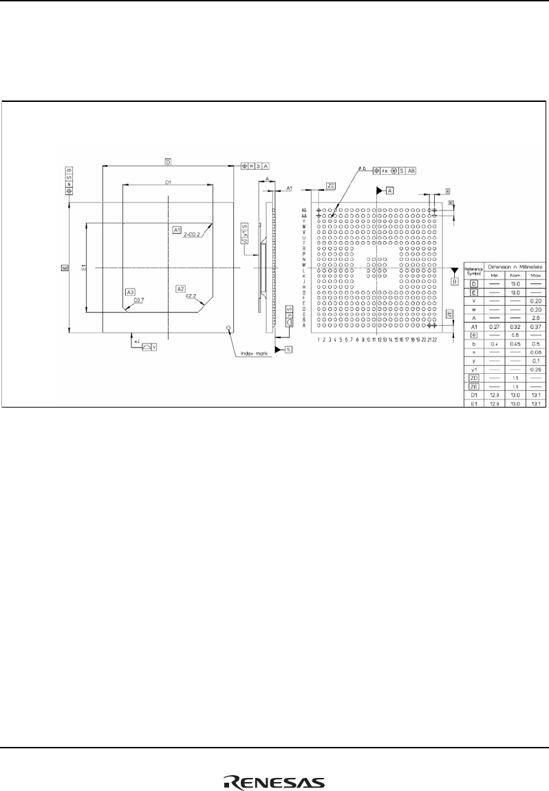
Appendix
Rev.1.00 Jan. 10, 2008 Page 1627 of 1658
REJ09B0261-0100
Appendix
A. Package Dimensions
Figure A.1 Package Dimensions (436-Pin BGA)
Note: The Tj (junction temperature) of this LSI becomes over 125°C. So a careful thermal
design is necessary. Use a heat sink or forced air cooling to lower the Tj.

Appendix
Rev.1.00 Jan. 10, 2008 Page 1628 of 1658
REJ09B0261-0100
B. Mode Pin Settings
The MODE14–MODE0 pin values are input in the event of a power-on reset via the PRESET pin.
Note: The MODE6 pin is output state after power-on reset.
Legend:
H: High level input
L: Low level input
Table B.1 Clock Operating Modes with External Pin Combination
Pin Value
MODE [4:0]
Pin Number
OSC/
External
input
Frequency
[MHz]
Frequency
(vs. Input Clock)
Clock
Operating
Mode 4 3 2 1 0 Min Max
Divider
1
PLL
1 Ick Uck SHck GAck DUck Pck DDRck Bck
0 L L L L L × 36 × 18 × 18 × 9 × 9 × 3 × 18 × 6
1 L L L L H × 36 × 18 × 18 × 9 × 9 × 3/2 × 18 × 3/2
2 L L L H L × 36 × 12 × 12 × 6 × 6 × 3 × 12 × 6
3 L L L H H
12 17 × 1
× 36 × 12 × 12 × 6 × 6 × 3/2 × 12 × 3/2
16 H L L L L 23 34 × 1 × 36 × 18 × 9 × 9 × 9/2 × 9/2 × 3/2 × 9 × 3
17 H L L L H × 18 × 9 × 9 × 9/2 × 9/2 × 3/4 × 9 × 3/4
18 H L L H L × 18 × 6 × 6 × 3 × 3 × 3/2 × 6 × 3
19 H L L H H × 18 × 6 × 6 × 3 × 3 × 3/4 × 6 × 3/4
Note: When MODE12 or MODE11 is set to low level, DUck is stopped.
The division ratio of the divider 2 can be read out from FRQMR1.
For details, see section 15, Clock Pulse Generator (CPG).

Appendix
Rev.1.00 Jan. 10, 2008 Page 1629 of 1658
REJ09B0261-0100
Table B.2 Area 0 Memory Type and Bus Width
Pin Value
MODE7 MODE6*MODE5 Memory Interface Bus Width
L L L MPX interface 64 bits
H Setting prohibited Setting prohibited
H L Setting prohibited Setting prohibited
H MPX interface 32 bits
H L L SRAM interface 64 bits
H SRAM interface 8 bits
H L SRAM interface 16 bits
H SRAM interface 32 bits
Note: * The MODE6 pin is output state after power-on reset.
Table B.3 Endian
Pin Value
MODE8 Endian
L Big endian
H Little endian
Table B.4 Master/Slave
Pin Value
MODE9 Master/Slave
L Slave
H Master
Table B.5 Clock Input
Pin Value
MODE10 Clock Input
L External input clock
H Crystal resonator

Appendix
Rev.1.00 Jan. 10, 2008 Page 1630 of 1658
REJ09B0261-0100
Table B.6 Bus Mode
Pin Value
MODE12 MODE11 Bus Mode
L L PCI host bus bridge
H PCIC normal (non-host)
H L Local bus
H Display unit
Table B.7 Boot Address Mode
Pin Value
MODE13 Boot address Mode
L 29-bit address mode
H 32-bit address extended mode
Table B.8 Mode Control
Pin Value
MODE14 Mode
L Setting prohibited
H Normal operation
Table B.9 Mode Control
Pin Value
MPMD Mode
L Emulation support mode
H LSI operation mode
Note: When using emulation support mode, refer to the emulator manual of the SH7785.

Appendix
Rev.1.00 Jan. 10, 2008 Page 1631 of 1658
REJ09B0261-0100
C. Pin Functions
C.1 Pin States
Table C.1 Pin States in Reset, Power-Down State, and Bus-Released State
Reset
Pin Name
(LSI level)
Pin Name
(Module level)
Related
Module I/O
Power-
on Manual Sleep
Module
Standby
Bus
Release
A[25:0] A[25:0] LBSC O PZ K K ⎯ PZ/Z
D[31:24] (default) LBSC I/O Z K K ⎯ Z D[31:24]
Port F[7:0] GPIO I/O ⎯ K K ⎯ Z
D[23:16] (default) LBSC I/O Z K K ⎯ Z D[23:16]
Port G[7:0] GPIO I/O ⎯ K K ⎯ Z
D[15:0] D[15:0] LBSC I/O Z K K ⎯ Z
CS[6:0] CS[6:0] LBSC O H(m)/
PZ(s) *1
K K ⎯ PZ/Z
BACK/BSREQ
(default)
LBSC I/O H*2 K K ⎯ O BACK/BSREQ
Port M0 GPIO I/O ⎯ K K ⎯ O
BREQ/BSACK
(default)
LBSC I/O PZ K K ⎯ I BREQ/BSACK
Port M1 GPIO I/O ⎯ K K ⎯ I
BS BS LBSC O H(m)/
PZ(s) *1
K K ⎯ PZ/Z
R/W R/W LBSC O H(m)/
PZ(s) *1
K K ⎯ PZ/Z
RD/FRAME RD/FRAME LBSC O H(m)/
PZ(s) *1
K K ⎯ PZ/Z
RDY RDY LBSC I PI K K ⎯ I
WE0/REG WE0/REG LBSC O H(m)/
PZ(s) *1
K K ⎯ PZ/Z
WE1 WE1 LBSC O H(m)/
PZ(s) *1
K K ⎯ PZ/Z
WE2/IORD WE2/IORD LBSC O H(m)/
PZ(s) *1
K K ⎯ PZ/Z
WE3/IOWR WE3/IOWR LBSC O H(m)/
PZ(s) *1
K K ⎯ PZ/Z

Appendix
Rev.1.00 Jan. 10, 2008 Page 1632 of 1658
REJ09B0261-0100
Reset
Pin Name
(LSI level)
Pin Name
(Module level)
Related
Module I/O
Power
-on Manual Sleep
Module
Standby
Bus
Release
DACK0 Port K1(default) GPIO I/O PI K K ⎯ K
DACK0 DMAC O ⎯ O O K O
Port K0 (default) GPIO I/O PI K K ⎯ K DACK1
DACK1 DMAC O ⎯ O O K O
Port K5 (default) GPIO I/O PI K K ⎯ K
DACK2 DMAC O ⎯ O O O O
SCIF2_TXD SCIF O ⎯ PZ/Z O O O
MMCCMD MMCIF I/O ⎯ PI/I K K K
DACK2/
SCIF2_TXD/
MMCCMD/
SIOF_TXD
SIOF_TXD SIOF O
⎯ H K K K
Port K4 (default) GPIO I/O PI K K ⎯ K
DACK3 DMAC O ⎯ O O O O
SCIF2_SCK SCIF I/O ⎯ I K K K
MMCDAT MMCIF I/O ⎯ I K K K
DACK3/
SCIF2_SCK/
MMCDAT/
SIOF_SCK
SIOF_SCK SIOF I/O
⎯ L K K K
STATUS0
(default)
RESET O H H L H L
DRAK0 DMAC O ⎯ O O O O
STATUS0/
DRAK0
Port K7 GPIO I/O ⎯ K K K K
STATUS1
(default)
RESET O H H H L L
DRAK1 DMAC O ⎯ O O O O
STATUS1/
DRAK1
Port K6 GPIO I/O ⎯ K K K K
DRAK2/CE2A Port L5 (default) GPIO I/O PI K K K K
DRAK2 DMAC O ⎯ O O O O
CE2A LBSC O ⎯ K K K K

Appendix
Rev.1.00 Jan. 10, 2008 Page 1633 of 1658
REJ09B0261-0100
Reset
Pin Name
(LSI level)
Pin Name
(Module level)
Related
Module I/O
Power
-on Manual Sleep
Module
Standby
Bus
Release
Port K3 (default) GPIO I/O PI K K ⎯ K DREQ0
DREQ0 DMAC I ⎯ PI/I PI/I PI/I PI/I
Port K2 (default) GPIO I/O PI K K ⎯ K DREQ1
DREQ1 DMAC I ⎯ PI/I PI/I PI/I PI/I
Port L7 (default) GPIO I/O PI K K ⎯ K
DREQ2 DMAC I ⎯ PI/I PI/I PI/I PI/I
DREQ2/INTB
INTB PCIC I ⎯ K K ⎯ K
Port L6 (default) GPIO I/O PI K K ⎯ K
DREQ3 DMAC I ⎯ PI/I PI/I PI/I PI/I
DREQ3/INTC
INTC PCIC I ⎯ K K ⎯ K
MCLK[1:0] MCLK[1:0] DBSC2 O L K K ⎯ K
MCLK[1:0] MCLK[1:0] DBSC2 O L K K ⎯ K
MDQS[3:0] MDQS[3:0] DBSC2 I/O Z K K ⎯ K
MDQS[3:0] MDQS[3:0] DBSC2 I/O Z K K ⎯ K
MDM[3:0] MDQ[3:0] DBSC2 O H K K ⎯ K
MDQ[31:0] MDQ[31:0] DBSC2 I/O Z K K ⎯ K
MCKE MCKE DBSC2 O L K K ⎯ K
MCAS MCAS DBSC2 O L K K ⎯ K
MRAS MRAS DBSC2 O L K K ⎯ K
MCS MCS DBSC2 O L K K ⎯ K
MWE MWE DBSC2 O L K K ⎯ K
MODT MODT DBSC2 O L K K ⎯ K
MA[14:0] MA[14:0] DBSC2 O L K K ⎯ K
MBA[2:0] MBA[2:0] DBSC2 O L K K ⎯ K
MBKPRST MBKPRST DBSC2 I I K K ⎯ K

Appendix
Rev.1.00 Jan. 10, 2008 Page 1634 of 1658
REJ09B0261-0100
Reset
Pin Name
(LSI level)
Pin Name
(Module level)
Related
Module I/O
Power
-on Manual Sleep
Module
Standby
Bus
Release
AD[31:24] PCIC I/O PZ K K ⎯ K
D[63:56] LBSC I/O PZ K K ⎯ Z
D[63:56]/
AD[31:24] *3
Port A[7:0] GPIO I/O PZ K K ⎯ K
AD[23:18] PCIC I/O PZ K K ⎯ K
D[55:50] LBSC I/O PZ K K ⎯ Z
D[55:50]/
AD[23:18] *3
Port B[7:2] GPIO I/O PZ K K ⎯ K
AD[17:16] PCIC I/O PZ K K ⎯ K
D[49:48] LBSC I/O PZ K K ⎯ Z
DB[5:4] DU O PZ K K K K
D[49:48]/
AD[17:16]/
DB[5:4] *3
Port B[1:0] GPIO I/O ⎯ K K ⎯ K
AD[15:12] PCIC I/O PZ K K ⎯ K
D[47:44] LBSC I/O PZ K K ⎯ Z
DB[3:0] DU O PZ K K K K
D[47:44]/
AD[15:12]/
DB[3:0] *3
Port C[7:4] GPIO I/O ⎯ K K ⎯ K
AD[11:8] PCIC I/O PZ K K ⎯ K
D[43:40] LBSC I/O PZ K K ⎯ Z
DG[5:2] DU O PZ K K K K
D[43:40]/
AD[11:8]/
DG[5:2] *3
Port C[3:0] GPIO I/O ⎯ K K ⎯ K
AD[7:6] PCIC I/O PZ K K ⎯ K
D[39:38] LBSC I/O PZ K K ⎯ Z
DG[1:0] DU O PZ K K K K
D[39:38]/
AD [7:6]/
DG[1:0] *3
Port D[7:6] GPIO I/O ⎯ K K ⎯ K
AD[5:0] PCIC I/O PZ K K ⎯ K
D[37:32] LBSC I/O PZ K K ⎯ Z
DR[5:0] DU O PZ K K K K
D[37:32]/
AD[5:0]/
DR[5:0] *3
Port D[5:0] GPIO I/O ⎯ K K ⎯ K
CBE[3:0] PCIC I/O PZ K K ⎯ K
WE[7:4] LBSC O PZ K K ⎯ Z
WE[7:4]/
CBE [3:0] *3
Port R[3:0] GPIO I/O PZ K K ⎯ K
GNT0/GNTIN*3 GNT0/GNTIN PCIC I/O PZ K K ⎯ K
Port Q3 GPIO I/O PZ K K ⎯ K

Appendix
Rev.1.00 Jan. 10, 2008 Page 1635 of 1658
REJ09B0261-0100
Reset
Pin Name
(LSI level)
Pin Name
(Module level)
Related
Module I/O
Power
-on Manual Sleep
Module
Standby
Bus
Release
GNT3 PCIC O PZ K K ⎯ K
MMCCLK MMCIF O PZ K K K K
GNT3/
MMCCLK *3
Port E0 GPIO I/O PZ K K ⎯ K
GNT[2:1] PCIC O PZ K K ⎯ K GNT[2:1] *3
Port E1-E2 GPIO I/O PZ K K ⎯ K
REQ0/
REQOUT
PCIC I/O PZ K K ⎯ K REQ0/REQOUT*3
Port Q2 GPIO I/O PZ K K ⎯ K
REQ3 PCIC I PZ K K ⎯ K REQ3*3
Port E3 GPIO I/O PZ K K ⎯ K
REQ[2:1] PCIC I PZ K K ⎯ K REQ[2:1] *3
Port E4-E5 GPIO I/O PZ K K ⎯ K
DEVSEL PCIC I/O PZ K K ⎯ K
DCLKOUT DU O PZ K K ⎯ K
DEVSEL/
DCLKOUT*3
Port P5 GPIO I/O PZ K K ⎯ K
PCIFRAME PCIC I/O PZ K K ⎯ K
VSYNC DU I/O PZ K K ⎯ K
PCIFRAME/
VSYNC*3
Port P0 GPIO I/O PZ K K ⎯ K
IDSEL IDSEL PCIC I I I K ⎯ I
INTA PCIC I/O PZ K K ⎯ K INTA*3
Port Q4 GPIO I/O PZ K K ⎯ K
IRDY PCIC I/O PZ K K ⎯ K
HSYNC DU I/O PZ K K ⎯ K
IRDY/HSYNC*3
Port P1 GPIO I/O PZ K K ⎯ K
LOCK PCIC I/O PZ K K ⎯ K
ODDF DU I/O PZ K K ⎯ K
LOCK/ODDF*3
Port P3 GPIO I/O PZ K K ⎯ K
PAR PAR PCIC I/O PZ O K ⎯ O
PCICLK PCIC I I PI K ⎯ K PCICLK/
DCLKIN*4 DCLKIN DU I I PI K ⎯ K

Appendix
Rev.1.00 Jan. 10, 2008 Page 1636 of 1658
REJ09B0261-0100
Reset
Pin Name
(LSI level)
Pin Name
(Module level)
Related
Module I/O
Power
-on Manual Sleep
Module
Standby
Bus
Release
PCIRESET PCIRESET PCIC O L O K ⎯ O
PERR*3 PERR PCIC I/O PZ K K ⎯ K
Port Q1 GPIO I/O PZ K K ⎯ K
SERR PCIC I/O PZ K K ⎯ K SERR*3
Port Q0 GPIO I/O PZ K K ⎯ K
STOP PCIC I/O PZ K K ⎯ K
CDE DU O PZ K K ⎯ K
STOP/CDE*3
Port P4 GPIO I/O PZ K K ⎯ K
TRDY PCIC I/O PZ K K ⎯ K
DISP DU O PZ K K ⎯ K
TRDY/DISP*3
Port P2 GPIO I/O PZ K K ⎯ K
CLKOUT CLKOUT CPG O O K K ⎯ K
CLKOUTENB CLKOUTENB CPG O H K K ⎯ K
PRESET PRESET RESET I I I I ⎯ I
NMI NMI INTC I PI PI/I PI/I ⎯ PI/I
MRESETOUT
(default)
RESET O H L O ⎯ O MRESETOUT/
IRQOUT
IRQOUT INTC O H O O
⎯ O
IRQ/IRL[3:0] IRQ/IRL[3:0] INTC I PI I I ⎯ I
MODE0 (power-
on reset)
CPG I I ⎯ ⎯ ⎯ ⎯
Port L4 (default) GPIO I/O ⎯ K K ⎯ K
IRQ/IRL4 INTC I ⎯ I I ⎯ I
MODE0/
IRQ/IRL4/
FD4
FD4 FLCTL I/O
⎯ K K K K
MODE1 (power-
on reset)
CPG I I ⎯ ⎯ ⎯ ⎯
Port L3 (default) GPIO I/O ⎯ K K ⎯ K
MODE1
IRQ/IRL5/
FD5
IRQ/IRL5 INTC I
⎯ I I ⎯ I
FD5 FLCTL I/O ⎯ K K K K

Appendix
Rev.1.00 Jan. 10, 2008 Page 1637 of 1658
REJ09B0261-0100
Reset
Pin Name
(LSI level)
Pin Name
(Module level)
Related
Module I/O
Power
-on Manual Sleep
Module
Standby
Bus
Release
MODE2 (power-
on reset)
CPG I I ⎯ ⎯ ⎯ ⎯
Port L2 (default) GPIO I/O ⎯ K K ⎯ K
MODE2/
IRQ/IRL6/
FD6
IRQ/IRL6 INTC I ⎯ I I ⎯ I
FD6 FLCTL I/O ⎯ K K K K
MODE3
(POWER-ON
RESET)
CPG I/O I ⎯ ⎯ ⎯ ⎯
Port L1 (default) GPIO I/O ⎯ K K ⎯ K
IRQ/IRL7 INTC I ⎯ I I ⎯ I
MODE3/
IRQ/IRL7/
FD7
FD7 FLCTL I/O
⎯ K K K K
MODE4 (power-
on reset)
CPG I I ⎯ ⎯ ⎯ ⎯
Port N5 (default) GPIO I/O ⎯ K K ⎯ K
SCIF3_TXD SCIF O ⎯ Z O O O
MODE4/
SCIF3_TXD/
FCLE
FCLE FLCTL O
⎯ K K K K
MODE5 (power-
on reset)
LBSC I I ⎯ ⎯ ⎯ ⎯ MODE5/
SIOF_MCLK
SIOF_MCLK
(default)
SIOF I ⎯ I I I I
MODE6 (power-
on reset)
LBSC I I ⎯ ⎯ ⎯ ⎯ MODE6/
SIOF_SYNC
SIOF_SYNC
(default)
SIOF I/O ⎯ O*2 K K K
MODE7 (power-
on reset)
LBSC I I ⎯ ⎯ ⎯ ⎯
Port N4 (default) GPIO I/O ⎯ K K ⎯ K
SCIF3_RXD SCIF I ⎯ I I I I
MODE7/
SCIF3_RXD/
FALE
FALE FLCTL O
⎯ K K K K
MODE8 (power-
on reset)
LBSC I I ⎯ ⎯ ⎯ ⎯
Port N3 (default) GPIO I/O ⎯ K K ⎯ K
MODE8/
SCIF3_SCK/
FD0
SCIF3_SCK SCIF I/O
⎯ I K K K
FD0 FLCTL I/O ⎯ K K K K

Appendix
Rev.1.00 Jan. 10, 2008 Page 1638 of 1658
REJ09B0261-0100
Reset
Pin Name
(LSI level)
Pin Name
(Module level)
Related
Module I/O
Power
-on Manual Sleep
Module
Standby
Bus
Release
MDOE9 (power-
on reset)
LBSC I I ⎯ ⎯ ⎯ ⎯
Port N2 (default) GPIO I/O ⎯ K K ⎯ K
SCIF4_TXD SCIF O ⎯ Z O O O
MDOE9/
SCIF4_TXD/
FD1
FD1 FLCTL I/O ⎯ K K K K
MODE10
(power-on reset)
CPG I I ⎯ ⎯ ⎯ ⎯
Port N1 (default) GPIO I/O ⎯ K K ⎯ K
MODE10/
SCIF4_RXD/
FD2
SCIF4_RXD SCIF I ⎯ I I I I
FD2 FLCTL I/O ⎯ K K K K
MODE11
(power-on reset)
LBSC I I ⎯ ⎯ ⎯ ⎯
Port N0 (default) GPIO I/O ⎯ K K ⎯ K
SCIF4_SCK SCIF I/O ⎯ I K K K
MODE11/
SCIF4_SCK/
FD3
FD3 FLCTL I/O
⎯ K K K K
MODE12
(power-on reset)
LBSC I I ⎯ ⎯ ⎯ ⎯
Port L0 (default) GPIO I/O ⎯ K K ⎯ K
DRAK3 DMAC O ⎯ O O O O
MODE12/
DRAK3/
CE2B
CE2B LBSC O
⎯ K K K K
MODE13 MMU I I ⎯ ⎯ ⎯ ⎯
Port J0 (default) GPIO I/O ⎯ K K ⎯ K
TCLK TMU I ⎯ I I I I
MODE13(power-
on reset)/
TCLK/
IOIS16
IOIS16 LBSC I
⎯ K K K K
MODE14 MODE14 CPG I I I I I I
EXTAL EXTAL CPG I I I I ⎯ I
XTAL XTAL CPG O O O O ⎯ O
Port H4 (default) GPIO I/O PI K K ⎯ K
SCIF0_CTS SCIF I/O ⎯ I K K K
SCIF0_CTS/
INTD/
FCE INTD PCIC I
⎯ K K ⎯ K
FCE FLCTL O ⎯ O K K K

Appendix
Rev.1.00 Jan. 10, 2008 Page 1639 of 1658
REJ09B0261-0100
Reset
Pin Name
(LSI level)
Pin Name
(Module level)
Related
Module I/O
Power
-on Manual Sleep
Module
Standby
Bus
Release
Port H3 (default) GPIO I/O PI K K ⎯ K
SCIF0_RTS SCIF I/O ⎯ I K K K
HSPI_CS HSPI I/O ⎯ Z K K K
SCIF0_RTS/
HSPI_CS/
FSE
FSE FLCTL O ⎯ O K K k
Port H1 (default) GPIO I/O PI K K ⎯ K
SCIF0_RXD SCIF I ⎯ I I K I
SCIF0_RXD/
HSPI_RX/
FRB HSPI_RX HSPI I ⎯ I K K K
FRB FLCTL I ⎯ I K K K
Port H2 (default) GPIO I/O PI K K ⎯ K
SCIF0_SCK SCIF I/O ⎯ I K K K
HSPI_CLK HSPI I/O ⎯ Z K K K
SCIF0_SCK/
HSPI_CLK/
FRE
FRE FLCTL O
⎯ O K K K
Port H0 (default) GPIO I/O PI K K ⎯ K
SCIF0_TXD SCIF O ⎯ Z O K O
HSPI_TX HSPI O ⎯ Z K K K
SCIF0_TXD/
HSPI_TX/
FWE
FWE FLCTL O
⎯ O K K K
Port H6 (default) GPIO I/O PI K K ⎯ K SCIF1_RXD
SCIF1_RXD SCIF I ⎯ I I I I
Port H7 (default) GPIO I/O PI K K ⎯ K SCIF1_SCK
SCIF1_SCK SCIF I/O
⎯ I K K K
Port H5 (default) GPIO I/O PI Z K ⎯ K SCIF1_TXD
SCIF1_TXD SCIF O ⎯ K O K O
SCIF2_RXD
(default)
SCIF I PI I K K K SCIF2_RXD/
SIOF_RXD
SIOF_RXD SIOF I ⎯ I I I I
Port J3 (default) GPIO I/O PI K K ⎯ K SIOF_MCLK/
HAC_RES SIOF_MCLK SIOF I ⎯ I I I I
HAC_RES HAC O ⎯ O O O O

Appendix
Rev.1.00 Jan. 10, 2008 Page 1640 of 1658
REJ09B0261-0100
Reset
Pin Name
(LSI level)
Pin Name
(Module level)
Related
Module I/O
Power
-on Manual Sleep
Module
Standby
Bus
Release
Port J5 (default) GPIO I/O PI K K ⎯ K
SIOF_RXD SIOF I ⎯ I I I I
SIOF_RXD/
HAC0_SDIN/
SSI0_SCK HAC0_SDIN HAC I ⎯ I I I I
SSI0_SCK SSI I/O ⎯ K K K K
Port J2 (default) GPIO I/O PI K K ⎯ K
SIOF_SCK SIOF I/O ⎯ L K K K
HAC0_BITCLK HAC I ⎯ I I I I
SIOF_SCK/
HAC0_BITCLK/
SSI0_CLK
SSI0_CLK SSI I
⎯ I I I I
Port J4 (default) GPIO I/O PI K K ⎯ K
SIOF_SYNC SIOF I/O ⎯ L K K K
HAC0_SYNC HAC O ⎯ O O O O
SIOF_SYNC/
HAC0_SYNC/
SSI0_WS
SSI0_WS SSI I/O
⎯ I K K K
Port J6 (default) GPIO I/O PI K K ⎯ K
SIOF_TXD SIOF O ⎯ H K K K
HAC0_SDOUT HAC O ⎯ O O O O
SIOF_TXD/
HAC0_SDOUT/
SSI0_SDATA
SSI0_SDATA SSI I/O
⎯ I K K K
Port J1 (default) GPIO I/O PI K K ⎯ K
HAC1_BITCLK HAC I ⎯ I I I I
HAC1_BITCLK/
SSI1_CLK
SSI1_CLK SSI I ⎯ I I I I
Port J7 (default) GPIO I/O PI K K ⎯ K
SCIF5_TXD SCIF O ⎯ Z O O O
HAC1_SYNC HAC O ⎯ O O O O
SCIF5_TXD/
HAC1_SYNC/
SSI1_WS
SSI1_WS SSI I/O
⎯ I K K K
Port N7
(default)
GPIO I/O PI K K ⎯ K
SCIF5_RXD SCIF I ⎯ I I I I
SCIF5_RXD/
HAC1_SDIN/
SSI1_SCK
HAC1_SDIN HAC I ⎯ I I I I
SSI1_SCK SSI I/O ⎯ I K K K

Appendix
Rev.1.00 Jan. 10, 2008 Page 1641 of 1658
REJ09B0261-0100
Reset
Pin Name
(LSI level)
Pin Name
(Module level)
Related
Module I/O
Power
-on Manual Sleep
Module
Standby
Bus
Release
Port N6
(default)
GPIO I/O PI K K ⎯ K
SCIF5_SCK SCIF I/O ⎯ I K K K
HAC1_SDOUT HAC O ⎯ O O O O
SCIF5_SCK/
HAC1_SDOUT/
SSI1_SDATA
SSI1_SDATA SSI I/O ⎯ I K K K
ASEBRK/
BRKACK
ASEBRK/
BRKACK
H-UDI I/O PI PI/O PI/O ⎯ PI/O
TCK TCK H-UDI I PI PI PI PI PI
TRST TRST H-UDI I PI PI PI PI PI
TDI TDI H-UDI I PI PI PI PI PI
TMS TMS H-UDI I PI PI PI PI PI
TDO TDO H-UDI O O O O O O
AUDCK AUDCK H-UDI O O O O ⎯ O
AUDSYNC AUDSYNC H-UDI O O O O ⎯ O
AUDATA[3:0] AUDATA[3:0] H-UDI O O O O ⎯ O
MPMD MPMD H-UDI I I I I ⎯ I
Legend:
⎯: Disabled (not selected) or not supported
(m): LBSC master mode
(s): LBSC slave mode
I: Input
O: Output
H: High level output
L: Low level output
Z: High impedance state
PI: Input and pulled up with a built-in pull-up resistance.
PZ: High impedance and pulled up with a built-in pull-up resistance.
K: Retain the previous pin state.
POR: Power-on reset
Notes: 1. Depends on the MODE9 pin setting.
2. After power-or reset, this pin is output state. Must not input signals immediately after
power-on reset.
3. Depends on the settings of the MODE[12:11] pin and corresponding registers.
4. When the bus mode selected by MODE11/MODE12 pins is PCI host bus bridge or
PCIC normal (non-host), clock must be input to PCICLK pin. When the bus mode
selected by MODE11/MODE12 pins is local bus or display unit, PCICLK pin must be
pulled-up to VDDQ or pulled-down to GND.

Appendix
Rev.1.00 Jan. 10, 2008 Page 1642 of 1658
REJ09B0261-0100
C.2 Handling of Unused Pins
Table C.2 Treatment of Unused Pins
Pin Name (LSI level)
Pin Name
(Module level) Module I/O When Not in Use
A[25:0] A[25:0] LBSC O Open
D[31:24] (default) LBSC I/O D[31:24]
Port F[7:0] GPIO I/O
Open
D[23:16] (default) LBSC I/O D[23:16]
Port G[7:0] GPIO I/O
Open
D[15:8] D[15:8] LBSC I/O Open
D[7:0] D[7:0] LBSC I/O Must be used
CS[6:1] CS[6:1] LBSC O Open
CS0 CS0 LBSC O Must be used
BACK/BSREQ (default) LBSC I/O BACK/BSREQ
Port M0 GPIO I/O
Open
BREQ/BSACK (default) LBSC I/O BREQ/BSACK
Port M1 GPIO I/O
Pulled to VDDQ
BS BS LBSC O Open
R/W R/W LBSC O Open
RD/FRAME RD/FRAME LBSC O Open
RDY RDY LBSC I Pulled-down to VSS*1
WE0/REG WE0/REG LBSC O Open
WE1 WE1 LBSC O Open
WE2/IORD WE2/IORD LBSC O Open
WE3/IOWR WE3/IOWR LBSC O Open
Port K1(default) GPIO I/O DACK0
DACK0 DMAC O
Open
DACK1 Port K0 (default) GPIO I/O Open
DACK1 DMAC O

Appendix
Rev.1.00 Jan. 10, 2008 Page 1643 of 1658
REJ09B0261-0100
Pin Name (LSI level)
Pin Name
(Module level) Module I/O When Not in Use
Port K5 (default) GPIO I/O
DACK2 DMAC O
SCIF2_TXD SCIF O
MMCCMD MMCIF I/O
DACK2/
SCIF2_TXD/
MMCCMD/
SIOF_TXD
SIOF_TXD SIOF O
Open
Port K4 (default) GPIO I/O
DACK3 DMAC O
SCIF2_SCK SCIF I/O
MMCDAT MMCIF I/O
DACK3/
SCIF2_SCK/
MMCDAT/
SIOF_SCK
SIOF_SCK SIOF I/O
Open
STATUS0 (default) RESET O
DRAK0 DMAC O
STATUS0/
DRAK0
Port K7 GPIO I/O
Open
STATUS1 (default) RESET O
DRAK1 DMAC O
STATUS1/
DRAK1
Port K6 GPIO I/O
Open
Port L5 (default) GPIO I/O
DRAK2 DMAC O
DRAK2/CE2A
CE2A LBSC O
Open
Port K3 (default) GPIO I/O DREQ0
DREQ0 DMAC I
Open
Port K2 (default) GPIO I/O DREQ1
DREQ1 DMAC I
Open
Port L7 (default) GPIO I/O
DREQ2 DMAC I
DREQ2/INTB
INTB PCIC I
Open
DREQ3/INTC Port L6 (default) GPIO I/O Open
DREQ3 DMAC I
INTC PCIC I

Appendix
Rev.1.00 Jan. 10, 2008 Page 1644 of 1658
REJ09B0261-0100
Pin Name
(LSI level)
Pin Name
(Module level) Module I/O When Not in Use
MCLK[1:0] MCLK[1:0] DBSC2 O Open
MCLK[1:0] MCLK[1:0] DBSC2 O Open
MDQS[3:0] MDQS[3:0] DBSC2 I/O Open
MDQS[3:0] MDQS[3:0] DBSC2 I/O Open
MDM[3:0] MDQ[3:0] DBSC2 O Open
MDQ[31:0] MDQ[31:0] DBSC2 I/O Open
MCKE MCKE DBSC2 O Open
MCAS MCAS DBSC2 O Open
MRAS MRAS DBSC2 O Open
MCS MCS DBSC2 O Open
MWE MWE DBSC2 O Open
MODT MODT DBSC2 O Open
MA[14:0] MA[14:0] DBSC2 O Open
MBA[2:0] MBA[2:0] DBSC2 O Open
MBKPRST MBKPRST DBSC2 I Pulled-up to VDD-DDR
AD[31:24] PCIC I/O
D[63:56] LBSC I/O
D[63:56]/
AD[31:24]
Port A[7:0] GPIO I/O
Open*2
AD[23:18] PCIC I/O
D[55:50] LBSC I/O
D[55:50]/
AD[23:18]
Port B[7:2] GPIO I/O
Open*2
AD[17:16] PCIC I/O
D[49:48] LBSC I/O
Open*2
DB[5:4] DU O
D[49:48]/
AD[17:16]/
DB[5:4]
Port B[1:0] GPIO I/O
Open*2
AD[15:12] PCIC I/O
D[47:44] LBSC I/O
D[47:44]/
AD[15:12]/
DB[3:0]
DB[3:0] DU O
Open*2

Appendix
Rev.1.00 Jan. 10, 2008 Page 1645 of 1658
REJ09B0261-0100
Pin Name (LSI level)
Pin Name
(Module level) Module I/O When Not in Use
AD[11:8] PCIC I/O
D[43:40] LBSC I/O
DG[5:2] DU O
D[43:40]/
AD[11:8]/
DG[5:2]
Port C[3:0] GPIO I/O
Open*2
AD[7:6] PCIC I/O
D[39:38] LBSC I/O
DG[1:0] DU O
D[39:38]/
AD [7:6]/
DG[1:0]
Port D[7:6] GPIO I/O
Open*2
AD[5:0] PCIC I/O
D[37:32] LBSC I/O
DR[5:0] DU O
D[37:32]/
AD[5:0]/
DR[5:0]
Port D[5:0] GPIO I/O
Open*2
CBE[3:0] PCIC I/O
WE[7:4] LBSC O
WE[7:4]/
CBE [3:0]
Port R[3:0] GPIO I/O
Open*2
GNT0/GNTIN PCIC I/O GNT0/GNTIN
Port Q3 GPIO I/O
Open*2
GNT3 PCIC O
MMCCLK MMCIF O
GNT3/MMCCLK
Port E0 GPIO I/O
Open
GNT[2:1] PCIC O GNT[2:1]
Port E1-E2 GPIO I/O
Open
REQ0/REQOUT PCIC I/O REQ0/REQOUT
Port Q2 GPIO I/O
Open*2
REQ3 PCIC I REQ3
Port E3 GPIO I/O
Open*2 or pulled-up to VDDQ
when PCIC normal mode
REQ[2:1] PCIC I REQ[2:1]
Port E4-E5 GPIO I/O
Open*2 or pulled-up to VDDQ
when PCIC normal mode
DEVSEL PCIC I/O Open*3 DEVSEL/
DCLKOUT DCLKOUT DU O
Port P5 GPIO I/O

Appendix
Rev.1.00 Jan. 10, 2008 Page 1646 of 1658
REJ09B0261-0100
Pin Name (LSI level)
Pin Name
(Module level) Module I/O When Not in Use
PCIFRAME PCIC I/O
VSYNC DU I/O
PCIFRAME/
VSYNC
Port P0 GPIO I/O
Open*2
IDSEL IDSEL PCIC I Pulled-down to VSS
INTA PCIC I/O INTA
Port Q4 GPIO I/O
Open*2 or pulled-up to VDDQ
when PCIC normal mode
IRDY PCIC I/O
HSYNC DU I/O
IRDY/HSYNC
Port P1 GPIO I/O
Open*2
LOCK PCIC I/O
ODDF DU I/O
LOCK/ODDF
Port P3 GPIO I/O
Open*2
PAR PAR PCIC I/O Open*2
PCICLK PCIC I PCICLK/
DCLKIN DCLKIN DU I
When the bus mode selected
by MODE11 and MODE12
pins is a PCI host bus bridge
or a PCI normal (non-host)
mode, clock must be input to
the PCICLK pin.
When the bus mode selected
by MODE11 and MODE12
pins is a Local bus or Display
Unit mode, PCICLK pin must
be pulled-up to VDDQ or
pulled-down to GND.
PCIRESET PCIRESET PCIC O Open
PERR PCIC I/O PERR
Port Q1 GPIO I/O
Open*2
SERR PCIC I/O SERR
Port Q0 GPIO I/O
Open*2
STOP/CDE STOP PCIC I/O Open*2
CDE DU O
Port P4 GPIO I/O

Appendix
Rev.1.00 Jan. 10, 2008 Page 1647 of 1658
REJ09B0261-0100
Pin Name (LSI level)
Pin Name
(Module level) Module I/O When Not in Use
TRDY PCIC I/O
DISP DU O
TRDY/DISP
Port P2 GPIO I/O
Open*2
CLKOUT CLKOUT CPG O Open
CLKOUTENB CLKOUTENB CPG O Open
PRESET PRESET RESET I Must be used
NMI NMI INTC I Pulled-up to VDDQ
MRESETOUT RESET O MRESETOUT/
IRQOUT IRQOUT INTC O
Open
IRQ/IRL[3:0] IRQ/IRL[3:0] INTC I Pulled-up to VDDQ
MODE0 (power-on
reset)
CPG I Must be used during power-on
reset
Port L4 (default) GPIO I/O
IRQ/IRL4 INTC I
MODE0/
IRQ/IRL4/
FD4
FD4 FLCTL I/O
Open
MODE1 (power-on
reset)
CPG I Must be used during power-on
reset
Port L3 (default) GPIO I/O
IRQ/IRL5 INTC I
MODE1
IRQ/IRL5/
FD5
FD5 FLCTL I/O
Open
MODE2 (power-on
reset)
CPG I Must be used during power-on
reset
Port L2 (default) GPIO I/O
IRQ/IRL6 INTC I
MODE2/
IRQ/IRL6/
FD6
FD6 FLCTL I/O
Open
MODE3 (power-on
reset)
CPG I/O Must be used during power-on
reset
Port L1 (default) GPIO I/O Open
MODE3/
IRQ/IRL7/
FD7
IRQ/IRL7 INTC I
FD7 FLCTL I/O

Appendix
Rev.1.00 Jan. 10, 2008 Page 1648 of 1658
REJ09B0261-0100
Pin Name (LSI level)
Pin Name
(Module level) Module I/O When Not in Use
MODE4 (power-on
reset)
CPG I Must be used during power-on
reset
Port N5 (default) GPIO I/O
SCIF3_TXD SCIF O
MODE4/
SCIF3_TXD/
FCLE
FCLE FLCTL O
Open
MODE5/
SIOF_MCLK
MODE5 (power-on
reset)
LBSC I Must be used during power-on
reset
SIOF_MCLK SIOF I Open
MODE6 (power-on
reset)
LBSC I Must be used during power-on
reset
MODE6/
SIOF_SYNC
SIOF_SYNC SIOF I/O Open
MODE7 (power-on
reset)
LBSC I Must be used during power-on
reset
Port N4 (default) GPIO I/O
SCIF3_RXD SCIF I
MODE7/
SCIF3_RXD/
FALE
FALE FLCTL O
Open
MODE8 (power-on
reset)
LBSC I Must be used during power-on
reset
Port N3 (default) GPIO I/O
SCIF3_SCK SCIF I/O
MODE8/
SCIF3_SCK/
FD0
FD0 FLCTL I/O
Open
MDOE9 (power-on
reset)
LBSC I Must be used during power-on
reset
Port N2 (default) GPIO I/O
SCIF4_TXD SCIF O
MDOE9/
SCIF4_TXD/
FD1
FD1 FLCTL I/O
Open
MODE10 (power-on
reset)
CPG I Must be used during power-on
reset
Port N1 (default) GPIO I/O Open
MODE10/
SCIF4_RXD/
FD2
SCIF4_RXD SCIF I
FD2 FLCTL I/O

Appendix
Rev.1.00 Jan. 10, 2008 Page 1649 of 1658
REJ09B0261-0100
Pin Name (LSI level)
Pin Name
(Module level) Module I/O When Not in Use
MODE11 (power-on
reset)
LBSC I Must be used during power-on
reset
Port N0 (default) GPIO I/O
SCIF4_SCK SCIF I/O
MODE11/
SCIF4_SCK/
FD3
FD3 FLCTL I/O
Open
MODE12 (power-on
reset)
LBSC I Must be used during power-on
reset
Port L0 (default) GPIO I/O
DRAK3 DMAC O
MODE12/
DRAK3/
CE2B
CE2B LBSC O
Open
MODE13 MMU I Must be used during power-on
reset
Port J0 (default) GPIO I/O
TCLK TMU I
MODE13/
TCLK/
IOIS16
IOIS16 LBSC I
Open
MODE14 MODE14 CPG I Must be used during power-on
reset (Pulled-up to VDDQ)
EXTAL EXTAL CPG I Must be used
XTAL XTAL CPG O Open
Port H4 (default) GPIO I/O
SCIF0_CTS SCIF I/O
INTD PCIC I
SCIF0_CTS/
INTD/
FCE
FCE FLCTL O
Open
Port H3 (default) GPIO I/O
SCIF0_RTS SCIF I/O
HSPI_CS HSPI I/O
SCIF0_RTS/
HSPI_CS/
FSE
FSE FLCTL O
Open
Port H1 (default) GPIO I/O Open
SCIF0_RXD SCIF I
SCIF0_RXD/
HSPI_RX/
FRB
HSPI_RX HSPI I
FRB FLCTL I

Appendix
Rev.1.00 Jan. 10, 2008 Page 1650 of 1658
REJ09B0261-0100
Pin Name (LSI level)
Pin Name
(Module level) Module I/O When Not in Use
Port H2 (default) GPIO I/O
SCIF0_SCK SCIF I/O
HSPI_CLK HSPI I/O
SCIF0_SCK/
HSPI_CLK/
FRE
FRE FLCTL O
Open
Port H0 (default) GPIO I/O
SCIF0_TXD SCIF O
HSPI_TX HSPI O
SCIF0_TXD/
HSPI_TX/
FWE
FWE FLCTL O
Open
Port H6 (default) GPIO I/O SCIF1_RXD
SCIF1_RXD SCIF I
Open
Port H7 (default) GPIO I/O SCIF1_SCK
SCIF1_SCK SCIF I/O
Open
Port H5 (default) GPIO I/O SCIF1_TXD
SCIF1_TXD SCIF O
Open
SCIF2_RXD (default) SCIF I SCIF2_RXD/
SIOF_RXD SIOF_RXD SIOF I
Open
Port J3 (default) GPIO I/O
SIOF_MCLK SIOF I
SIOF_MCLK/
HAC_RES
HAC_RES HAC O
Open
Port J5 (default) GPIO I/O
SIOF_RXD SIOF I
HAC0_SDIN HAC I
SIOF_RXD/
HAC0_SDIN/
SSI0_SCK
SSI0_SCK SSI I/O
Open
Port J2 (default) GPIO I/O
SIOF_SCK SIOF I/O
HAC0_BITCLK HAC I
SIOF_SCK/
HAC0_BITCLK/
SSI0_CLK
SSI0_CLK SSI I
Open
Port J4 (default) GPIO I/O
SIOF_SYNC SIOF I/O
SIOF_SYNC/
HAC0_SYNC/
SSI0_WS HAC0_SYNC HAC O
Open
SSI0_WS SSI I/O

Appendix
Rev.1.00 Jan. 10, 2008 Page 1651 of 1658
REJ09B0261-0100
Pin Name (LSI level)
Pin Name
(Module level) Module I/O When Not in Use
Port J6 (default) GPIO I/O
SIOF_TXD SIOF O
HAC0_SDOUT HAC O
SIOF_TXD/
HAC0_SDOUT/
SSI0_SDATA
SSI0_SDATA SSI I/O
Open
Port J1 (default) GPIO I/O
HAC1_BITCLK HAC I
HAC1_BITCLK/
SSI1_CLK
SSI1_CLK SSI I
Open
Port J7 (default) GPIO I/O
SCIF5_TXD SCIF O
HAC1_SYNC HAC O
SCIF5_TXD/
HAC1_SYNC/
SSI1_WS
SSI1_WS SSI I/O
Open
Port N7 GPIO I/O
SCIF5_RXD SCIF I
HAC1_SDIN HAC I
SCIF5_RXD/
HAC1_SDIN/
SSI1_SCK
SSI1_SCK SSI I/O
Open
Port N6 GPIO I/O
SCIF5_SCK SCIF I/O
HAC1_SDOUT HAC O
SCIF5_SCK/
HAC1_SDOUT/
SSI1_SDATA
SSI1_SDATA SSI I/O
Open
THDAG THDAG ⎯ ⎯ Connected to VSS
THDAS THDAS ⎯ ⎯ Connected to VSS
THDCTL THDCTL ⎯ ⎯ Connected to VSS
THDCD THDCD ⎯ ⎯ Connected to VSS
VDDQ-TD VDDQ-TD ⎯ ⎯ Connected to VSS or VDDQ
ASEBRK/
BRKACK
ASEBRK/
BRKACK
H-UDI I/O Open
TCK TCK H-UDI I Open
TRST TRST H-UDI I Pulled-down to VSS or
connected to PRESET*4
TDI TDI H-UDI I Open
TMS TMS H-UDI I Open
TDO TDO H-UDI O Open

Appendix
Rev.1.00 Jan. 10, 2008 Page 1652 of 1658
REJ09B0261-0100
Pin Name (LSI level)
Pin Name
(Module level) Module I/O When Not in Use
AUDCK AUDCK H-UDI O Open
AUDSYNC AUDSYNC H-UDI O Open
AUDATA[3:0] AUDATA[3:0] H-UDI O Open
MPMD MPMD H-UDI I Pulled-up to VDDQ
Notes: Power must be supplied to each power supply pin, even when the function pin is not used.
When a pin is not used, do not set the register for the pin.
1. This pin is pulled-up within this LSI after power-on reset. Set the RDYPUP bit in
PPUPR1 (GPIO) to 1 to pull-up off the RDY pin's pulled-up.
2. The MODE[12:11] pin settings should be LBSC mode to be open these pins.
3. Specify LBSC mode or DU mode by the MODE[12:11] pins.
4. When not using emulator, the pin should be fixed to ground or connected to another pin
which operates in the same manner as PRESET. However, when fixed to a ground pin,
the following problem occurs. Since the TRST pin is pulled up within this LSI, a weak
current flows when the pin is externally connected to ground pin. The value of the
current is determined by a resistance of the pull-up MOS for the port pin. Although this
current does not affect the operation of this LSI, it consumes unnecessary power.
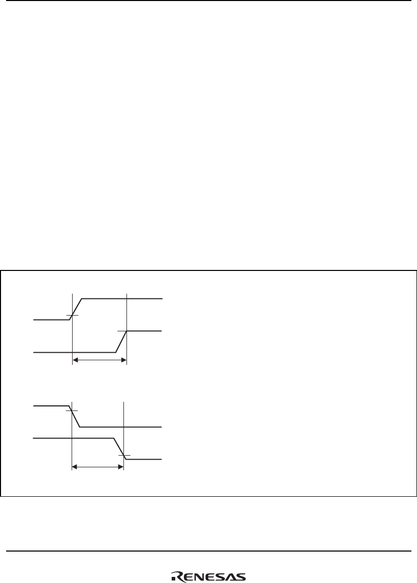
Appendix
Rev.1.00 Jan. 10, 2008 Page 1653 of 1658
REJ09B0261-0100
D. Turning On and Off Power Supply
D.1 Turning On and Off Between Each Power Supply Series
The order of the power supply between the 1.0V series power supply (VDD10: VDD and VDD-
PLL1 to 2 and VDDA-PLL1), the 1.8V series power supply (VDD18: VDD-DDR) and the 3.3V
series power supply (VDD33: VDDQ and VDDQ-PLL1 to 2 and VDDQ-TD*) is as follows.
Note: * If VDDQ-TD is connected to VDDQ.
• Turning On Power Supply
There is no restriction for the order of the power supply between each power supply series
(VDD10, VDD18, VDD33). Within 300 ms after turning on one power supply series, turn on
all the other power supply series.
• Turning Off Power Supply
There is no restriction for the order of the power supply between each power supply series.
(VDD10, VDD18, VDD33). Within 300 ms after turning off the one power supply series, turn
off all the other power supply series.
300 > t > or = 0
[ms]
0.1 × V**
V** min
0.9 × V**
0.2 [V]
V**:
VDD10, VDD18 (transition from DDR power supply backup), VDD33
V**:
VDD10, VDD18 (transition from DDR power supply backup), VDD33
300 > t > or = 0
[ms]
VDD10: VDD, VDD-PLL1 to 2, VDDA-PLL1
VDD18: VDD-DDR (except DDR2-SDRAM backup to turning on)
VDD33: VDDQ, VDDQ-PLL1 to 2, VDDQ-TD*
Note: * If VDDQ-TD is connected to VDDQ.
Turning on
Turning off
Figure D.1 Sequence of Turning On and Off Each Power Supply
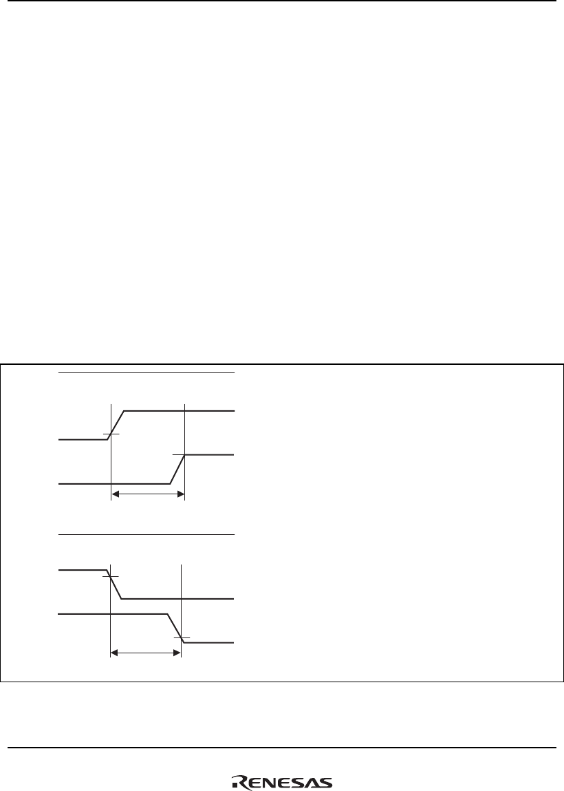
Appendix
Rev.1.00 Jan. 10, 2008 Page 1654 of 1658
REJ09B0261-0100
D.2 Power-On and Power-Off Sequences for Power Supplies with Different Potentials in
DDR2-SDRAM Power Supply Backup Mode
The power-on and power-off sequences for the 1.0 V power supply (VDD10 using pins VDD,
VDD-PLL1, VDDA-PLL1, and VDD-PLL2), 1.8 V power supply (VDD18 using pin VDD-DDR),
and 3.3 V power supply (VDD33 using pins VDDQ, VDDQ-PLL1, VDDQ-PLL2, and VDDQ-
TD*) in DDR2-SDRAM power supply backup mode are as follows.
Note: * If VDDQ-TD is connected to VDDQ.
• Power-On Sequence
There is no restriction on the sequence in which the above power supplies are powered on.
Ensure that all the power supplies start within 300 ms of the start of a power supply other than
VDD-DDR.
• Power-Off Sequence
There is no restriction on the sequence in which the above power supplies are powered off.
Ensure that all the power supplies stop within 300 ms of the stop of a power supply other than
VDD-DDR.
300ms > t ≥ 0s
300ms > t ≥ 0s
0.1 × V**
V** min
0.9 × V**
0.2 [V]
V**: VDD10,VDD33
V**: VDD10, VDD18, VDD33
VDD18 = ON
VDD18 = ON
VDD10 (pins: VDD, VDD-PLL1, VDDA-PLL1, VDD-PLL2)
VDD33 (pins: VDDQ, VDDQ-PLL1, VDDQ-PLL2, VDDQ-TD*)
Note: * If VDDQ-TD is connected to VDDQ.
Figure D.2 Power-On and Power-Off Sequences for Power Supplies with Different
Potentials in DDR2-SDRAM Power Supply Backup Mode
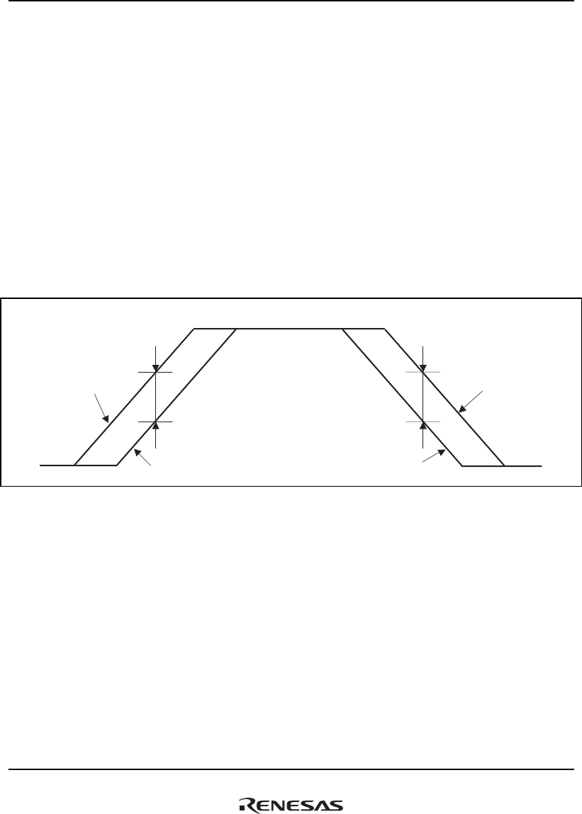
Appendix
Rev.1.00 Jan. 10, 2008 Page 1655 of 1658
REJ09B0261-0100
D.3 Turning On and Off Between the Same Power Supply Series
The order of the power supply in the VDD10 series, the VDD18 series and the VDD33 series
power supply is as follows.
Figure D.3 is an explanation chart of VDD10. The regulation of the potential difference is the
same VDD10 as the other (VDD10, VDD33).
• Turning On Power Supply
There is no restriction for the order of the power supply between each power supply series
except that the potential difference of the one power supply series is less than 0.3V.
• Turning Off Power Supply
There is no restriction for the order of the power supply between each power supply series
except that the potential difference of the one power supply series is less than 0.3V.
V**: VDD10: VDD, VDD-PLL 1 to 2, VDDA-PLL1
Turning on Tuurning off
V**
V**
0.3V (max)
V**
V**
0.3V (max)
Figure D.3 Sequence of Turning On and Off VDD10 Power Supply Series
Appendix
Rev.1.00 Jan. 10, 2008 Page 1656 of 1658
REJ09B0261-0100
E. Version Registers (PVR, PRR)
The SH7785 has the read-only registers which show the version of a processor core, and the
version of a product. By using the value of these registers, it becomes possible to be able to
distinguish the version and product of a processor from software, and to realize the scalability of
the high system. Since the values of the version registers differ for every product, please refer to
the hardware manual or contact Renesas Technology Corp.
Note: The bit 7 to bit 0 of PVR register and the bit 3 to bit 0 of PRR register should be masked
by the software.
Table E.1 Register Configuration
Register Name Abbrev. R/W
Initial
Value
P4
Address
Area 7
Address
Access
Size
Processor Version Register PVR R H'1030 07xx H'FF00 0030 H'1F00 0030 32
Product Register PRR R H'0000 02xx H'FF00 0044 H'1F00 0044 32
Legend:
x: Undefined
• Processor Version Register (PVR)
31 30 29 28 27 26 25 24 23 22 21 20 19 18 17 16
Bit:
version information
version information
0001000000110000
Initial value
RRRRRRRRRRRRRRRR
R/W:
Bit:
Initial value
R/W:
1514131211109876543210
0000
0111
RRRRRRRR
• Product Register (PRR)
31 30 29 28 27 26 25 24 23 22 21 20 19 18 17 16
Bit:
version information
version information
0000000000000000
Initial value
RRRRRRRRRRRRRRRR
R/W:
Bit:
Initial value
R/W:
1514131211109876543210
00000010
RRRRRRRR

Appendix
Rev.1.00 Jan. 10, 2008 Page 1657 of 1658
REJ09B0261-0100
F. Product Lineup
Table F.1 SH7785 Product Lineup
Product
Type Voltage
Operating
Frequency Part Number
Operating
Temperature Package
SH7785 1.1 V 600 MHz R8A77850AADBG −40 to 85°C 436-pin BGA
R8A77850AADBGV 436-pin BGA
(Lead Free)
R8A77850ANBG −20 to 85°C 436-pin BGA
R8A77850ANBGV 436-pin BGA
(Lead Free)

Appendix
Rev.1.00 Jan. 10, 2008 Page 1658 of 1658
REJ09B0261-0100

Renesas 32-Bit RISC Microcomputer
Hardware Manual
SH7785
Publication Date: Rev.1.00, January 10, 2008
Published by: Sales Strategic Planning Div.
Renesas Technology Corp.
Edited by: Customer Support Department
Global Strategic Communication Div.
Renesas Solutions Corp.
© 2008. Renesas Technology Corp., All rights reserved. Printed in Japan.

Sales Strategic Planning Div. Nippon Bldg., 2-6-2, Ohte-machi, Chiyoda-ku, Tokyo 100-0004, Japan
http://www.renesas.com
Refer to "http://www.renesas.com/en/network" for the latest and detailed information.
Renesas Technology America, Inc.
450 Holger Way, San Jose, CA 95134-1368, U.S.A
Tel: <1> (408) 382-7500, Fax: <1> (408) 382-7501
Renesas Technology Europe Limited
Dukes Meadow, Millboard Road, Bourne End, Buckinghamshire, SL8 5FH, U.K.
Tel: <44> (1628) 585-100, Fax: <44> (1628) 585-900
Renesas Technology (Shanghai) Co., Ltd.
Unit 204, 205, AZIACenter, No.1233 Lujiazui Ring Rd, Pudong District, Shanghai, China 200120
Tel: <86> (21) 5877-1818, Fax: <86> (21) 6887-7858/7898
Renesas Technology Hong Kong Ltd.
7th Floor, North Tower, World Finance Centre, Harbour City, Canton Road, Tsimshatsui, Kowloon, Hong Kong
Tel: <852> 2265-6688, Fax: <852> 2377-3473
Renesas Technology Taiwan Co., Ltd.
10th Floor, No.99, Fushing North Road, Taipei, Taiwan
Tel: <886> (2) 2715-2888, Fax: <886> (2) 3518-3399
Renesas Technology Singapore Pte. Ltd.
1 Harbour Front Avenue, #06-10, Keppel Bay Tower, Singapore 098632
Tel: <65> 6213-0200, Fax: <65> 6278-8001
Renesas Technology Korea Co., Ltd.
Kukje Center Bldg. 18th Fl., 191, 2-ka, Hangang-ro, Yongsan-ku, Seoul 140-702, Korea
Tel: <82> (2) 796-3115, Fax: <82> (2) 796-2145
Renesas Technology Malaysia Sdn. Bhd
Unit 906, Block B, Menara Amcorp, Amcorp Trade Centre, No.18, Jln Persiaran Barat, 46050 Petaling Jaya, Selangor Darul Ehsan, Malaysia
Tel: <603> 7955-9390, Fax: <603> 7955-9510
RENESAS SALES OFFICES
Colophon 6.2

SH7785
Hardware Manual
