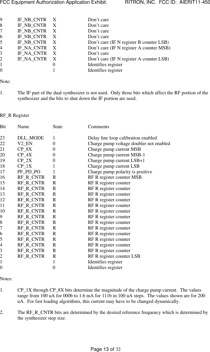
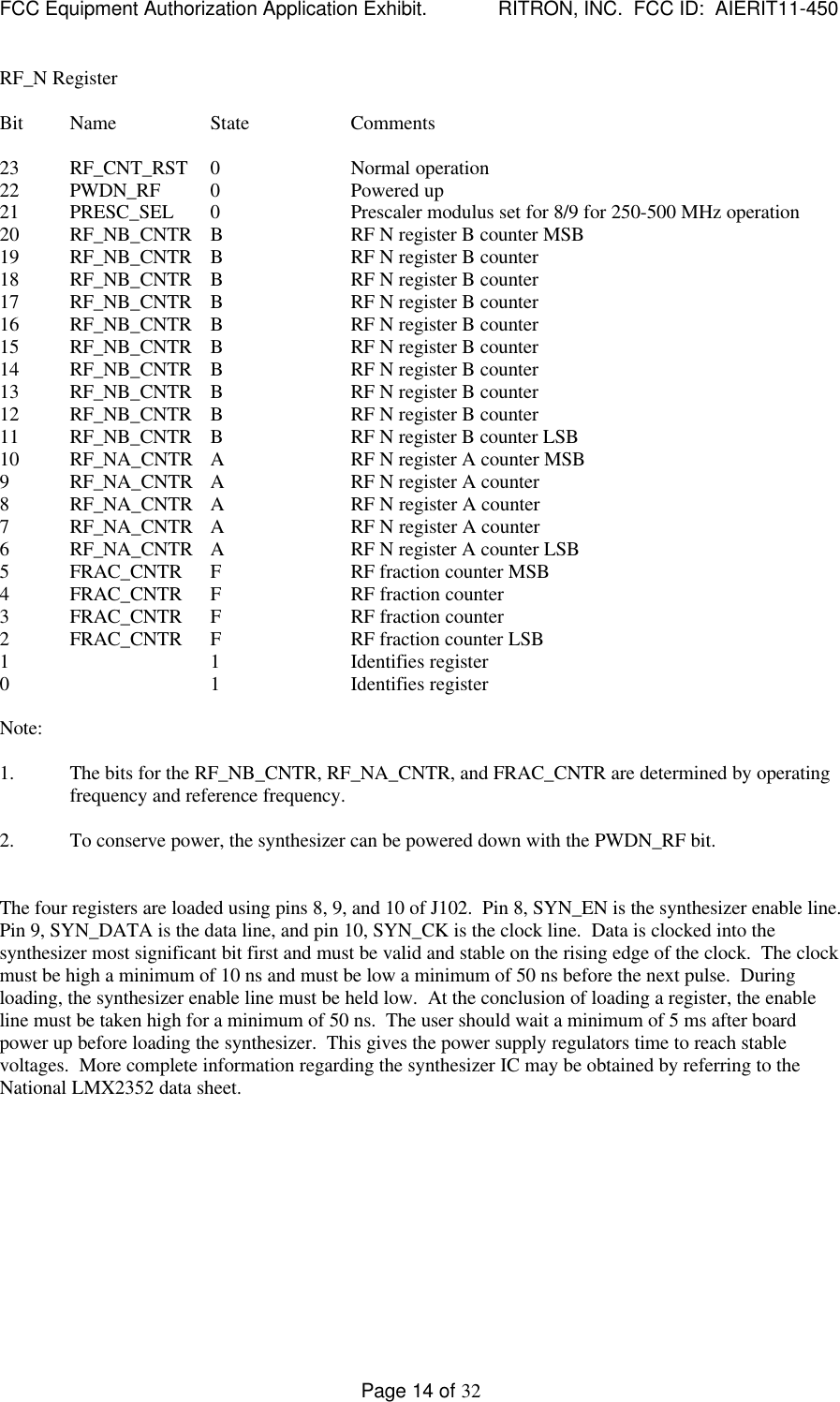
Ritron RIT11-450 Two Way Radio Transceiver Module User Manual Instruction Manual

Ritron Inc Two Way Radio Transceiver Module Instruction Manual

Instruction Manual

FCC Equipment Authorization Application Exhibit.             RITRON, INC.  FCC ID:  AIERIT11-450Page 1 of 32TYPE OF EXHIBIT:INSTRUCTION BOOK (PRELIMINARY)FCC PART:2.983 (d) (8)MANUFACTURER:RITRON, INC.505 West Carmel DriveCarmel, IN 46032MODEL:DTX-454TYPE OF UNIT:UHF-FM TransceiverFCC ID: AIERIT11-450DATE: February 2, 1999Preliminary Instruction Book follows.
FCC Equipment Authorization Application Exhibit.             RITRON, INC.  FCC ID:  AIERIT11-450Page 2 of 32RITRON, INC.RITRON MODEL DTX-454PROGRAMMABLE FM TRANSCEIVERMODULEMAINTENANCE& OPERATINGMANUALFOR USE ONLY BY AUTHORIZED SERVICE/MAINTENANCE PERSONNEL
FCC Equipment Authorization Application Exhibit.             RITRON, INC.  FCC ID:  AIERIT11-450Page 3 of 32DTX454 SPECIFICATIONSGENERALFCC Identifier AIERIT11-450 (pending)FCC Rule Parts 22, 74, 90, 95Frequency Range 400-420 MHz *420-440 MHz *430-450 MHz *450-470 MHz470-490 MHz *490-512 MHz *Number of Channels 8Transmit/Receive Spacing 20 MHz max.Mode of Operation Simplex or Half DuplexFrequency Control PLL SynthesizerChannel Increment (Synthesizer step size) 5/6.25 kHzEmissions BandwidthNarrow Mode 11 kHzWide Mode 16 kHzFrequency Stability (-30 to +65C) 1.5 ppmSupply Voltage6 watt versionw/o internal regulator 7.5 VDCw internal regulator 11-16 VDC10 watt version 11.5 to 15  VDCRF Input/Output Connector BNCPower/Data Interface 15 pin subminiature D typeOperating Temperature -30 to +65 CMaximum Dimensions (L x W x H) 3.6” x 2.3” x 1.0” including connectorsWeight 6 oz.* Not Available Yet
FCC Equipment Authorization Application Exhibit.             RITRON, INC.  FCC ID:  AIERIT11-450Page 4 of 32TRANSMITTEROperating Bandwidth 20 MHzRF Output Power6 watt version 1 to 6 watts, adjustable10 watt version 1 to 10 watts, adjustableDuty Cycle 5 to 100 % depending upon heatsink andpower levelRF Load Impedance 50 ohmsModulation Distortion (per TIA/EIA 603) 5 % max.Modulation Frequency Response (+1/-3 dB ref 1 kHz)At MIC IN (ref pre-emphasis curve) 50 Hz to 2500 HzAt AUX IN w/o pre-emphasis 50 Hz to 2700 HzTransmitter Attack Time:To within 2.5 ppm final frequency 10 ms max.To within 0.5 ppm final frequency 15 ms max.Spurious and Harmonics -20 dBm max.FM Hum and Noise (per TIA/EIA 603)12.5 kHz channel operation 40 dB min.25 kHz channel operation 45 dB min.Group Delay Variation (Within Frequency Response) 5 us max.Current Drain6 watt version at 7.5 VDC supply1 watt 1.0 A max.6 watts 2.4 A max.10 watt version at 13.7 VDC supply1 watt 0.7 A max.10 watts 2.4 A max.
FCC Equipment Authorization Application Exhibit.             RITRON, INC.  FCC ID:  AIERIT11-450Page 5 of 32RECEIVEROperating Bandwidth 20 MHzSensitivity (12 SINAD w de-emphasis) 0.30 uV (-117.5 dBm)RF Input Impedance 50 ohmsAdjacent Channel Selectivity+/- 12.5 kHz w narrow IF 60 dB min.+/- 25 kHz w wide IF 70 dB min.Spurious and Image Rejection 70 dB min.Intermodulation Rejection 70 dB min.FM Hum and Noise (per TIA/EIA 603)12.5 kHz channel operation 40 dB min.25 kHz channel operation 45 dB min.Conducted Spurious -57 dBm max.Receive Attack Time 15 ms max.Audio Distortion (per TIA/EIA 603) 5 % max.Audio Response at AUX OUT (+1/-3 dB, ref 1 kHz)12.5 kHz channel operation 100 Hz to 3.5 kHz25 kHz channel operation 100 Hz to 5 kHzGroup Delay Variation (Within Frequency Response) 20 us max.Receive Current Drain 75 mA max.
FCC Equipment Authorization Application Exhibit.             RITRON, INC.  FCC ID:  AIERIT11-450Page 6 of 32DTX-154/454  INPUT/OUTPUT CONNECTORPin Number Name Description Comments1CS0 Channel Select low bit2CS1 Channel Select mid bit3CS2 Channel Select high bit4MIC IN Microphone Input Input for microphone type signalsto be transmitted.  Signals at thisinput are pre-emphasized, limited,and filtered.5CSN Channel Select6RAW SUPPLY Power Supply Input Positive Supply voltage input.7AUX IN Auxiliary Input Wideband input for data.8AUX OUT Auxiliary Output Wideband output for data.9PGN IN/OUT Programming I/O External programmer connectshere.10. CTS Clear to Send Active high when transmittercan accept modulation.11. RX MON Monitor Breaks squelch in receive.12. AUDIO OUT Audio PA Output Output of audio PA.13. DCD Carrier Detect Carrier detect output.14. PTT RTS Push to Talk Activates transmitter.15. GND Ground Negative supply point andreference for all inputs.
FCC Equipment Authorization Application Exhibit.             RITRON, INC.  FCC ID:  AIERIT11-450Page 7 of 32Pin Number Description1 CS0-Least significant bit of the channel select lines.  Active high 5 volt TTL/CMOSlevel.2 CS1-Mid bit of the channel select lines.  Active high 5 volt TTL/CMOS level.3 CS2-Most significant bit of the channel select lines.  Active high 5 volt TTL/CMOSlevel.Channel CS0 CS1 CS21 0 0 02 0 0 13 0 1 04 0 1 15 1 0 06 1 0 17 1 1 08 1 1 10 = Logic low1 = Logic high4 MIC IN-Microphone input.  This input accepts microphone type input signals fortransmit  The signal is amplified, passed through the clipper and the clipper filter andthen to the RF board.  This input can be programmed to be disabled (muted) if desired.5 CSN-When enabled through programming, this input selects between channels 1 and 2.This input is TTL/CMOS level type input with a logic low required for channel 1 and alogic high required for channel 2.6 RAW SUPPLY- The positive supply voltage for the unit is supplied through this pin.The actual supply voltage required depends upon model type.  Ensure that the correctsupply voltage per the given model is used.7 AUX IN-This is the broadband input for modulation.  The gain through this input to themodulator is programmable as is the use of pre-emphasis.  This signal passes through theclipper and clipper filter.8 AUX OUT-This is the broadband output of the receiver.  The gain from the receiver tothe output is programmable as is the use of de-emphasis.  The choice of AC or DCcoupling from the RF board discriminator is also programmable.9 PGN IN/OUT-Connect via Ritron RPT-PCPK PC Programming Kit to computer forprogramming the unit.10 CTS-Clear-To-Send output from the unit which indicates that the unit is transmitting acarrier at the correct frequency and power level and is ready to accept an input signal tobe transmitted.  This output would normally become active in response to a PTT RTS(see pin 14 description below) activation.  The polarity of this output can be programmed.The output is active low 5 volt logic with an internal 10 k ohm pull-up to 5 volts.  It cansource up to 10 mA when low.
FCC Equipment Authorization Application Exhibit.             RITRON, INC.  FCC ID:  AIERIT11-450Page 8 of 3211 RX MON-This input breaks the squelch on the receiver i.e. allows for monitoring thechannel, even when a signal not strong enough to break squelch is present.  Input levelsare TTL/CMOS; polarity may be programmed.12 AUDIO OUT-This is the output of the audio power amplifier.  This output can drive upto ½ watt in to an 8 ohm load.  This output can be enabled and its gain controlled byprogramming.13 DCD-Carrier Detect Output.  This output becomes active when a signal strong enough toexceed the programmed squelch threshold is present.  The polarity of this output can beprogrammed.  The output is active low 5 volt logic with an internal 10 k ohm pull-up to 5volts.  It can source up to 10 mA when low.14 PTT RTS-Push To Talk/Request To Send.  This input commands the unit to transmit.Input levels are TTL/CMOS; polarity may be programmed.15 GND-System ground.  All signals and voltages are referenced to this input.  The negativeside of the power supply should connect here.
FCC Equipment Authorization Application Exhibit.             RITRON, INC.  FCC ID:  AIERIT11-450Page 9 of 32RF BOARD J301 INPUT/OUTPUTPin Number Name DescriptionJ102-0                  PWR_SET When PC board jumper R185 is installed and R186 omitted (normalwith the loader board connected), the voltage on this pin controls theRF output power.  When R186 is installed and R185 omitted(normalfor stand alone RF board), the RF output power is controlled by R187on the RF board and this pin has no function.  When this pin is used,the voltage should range between about 1 and 4.5 VDC to vary theoutput power from 1 to 5 watts.  The relationship between output powerand voltage is non-linear and may vary as a function of operatingfrequency.  The input resistance at this pin is approximately 15 k-ohm.J101-1 GND System ground.  All voltages are referenced to this point.J102-2                  FB+ Power supply input for the RF PA module.  Voltage at this pin dependsupon model and should be either +7.2 VDC +/- 10% or 11 to 16 VDC,and filtered .  Current drain can be as high as 2.5 amperes at maximumRF output.J102-3 TX_EN Active high, 5 volt CMOS logic level input used to enable thetransmitter driver stage and PA pin diodes.  Timing circuitry existson the RF board to ramp the PA power up or down to control keyingspurious outputs.J102-4 RX_EN Active high, 5 volt CMOS logic level input used to enable the receiverstages and to set the VCO to the receive frequency range.J102-5 XCVR_EN Active high, 5 volt logic level input used to enable all stages of theboard except the PA and PA driver stages.  This pin can be used toconserve current consumption in a battery save configuration.J102-6 MOD_IN Modulation input for the transmitter.  The modulating signal must besuperimposed upon a very stable and low noise 2.5 VDC level.Modulation sensitivity is approximately 14 kHz/V.  The inputresistance is approximately 17 k-ohm.  Note:  The DC voltage at thispin directly controls the frequency of the unit.  Therefore, the DCvoltage must be well regulated and controlled over environmentalconditions.J102-7 LOCK_DETECTLock detect output of the frequency synthesizer.  Output is at 5 voltlogic level with a high level indicating lock.J102-8 SYN_EN Enable line for loading the synthesizer.  Signal is at 5 volt CMOS logiclevels.J102-9 SYN_DATA Data line for loading the synthesizer.  Signal is at 5 volt CMOS logiclevels.J102-10 SYN_CK Clock line for loading the synthesizer.  Signal is at 5 volt CMOS logiclevels.J102-11 +7.2V +7.2 VDC +/- 10 % input for powering all stages of the radio exceptRF PA module.  Current drain is approximately 45 mA in receive and
FCC Equipment Authorization Application Exhibit.             RITRON, INC.  FCC ID:  AIERIT11-450Page 10 of 32100 mA in transmit.J102-12 RSSI Receive signal strength indicator output.  This is a high impedanceoutput which is used to indicate the presence of a carrier.  When R124is installed (R125 omitted), the output will vary betweenapproximately 0.5 VDC and 3.0 VDC as the input signal level variesbetween –130 dBm and –70 dBm.  When R125 is installed (R124omitted), the output will vary between approximately 2.5 VDC at 0dB SINAD and 0.5 VDC at 20 dB SINAD.  The loading on this outputmust be kept above 100 k-ohm.J102-13 DISC_OUT DC coupled discriminator output.  The polarity of this output iscontrolled by R131 and R132.  For positive polarity i.e. an increasein carrier frequency causes the DC level to increase, R131 should beinstalled and R132 omitted.  For negative polarity, R132 should beinstalled and R1431 omitted.  The output is low impedance with amodulation sensitivity of approximately 0.5 V/kHz for narrow bandunits and 0.25 V/kHz for wide band units.  The DC level at this pinis typically between 2 and 4 volts.J102-14              VCO_MOD When R179 is installed and R178 omitted (normal with loader boardattached), a signal at this pin will modulate the VCO.  When R178 isinstalled and R179 omitted (normal for stand alone RF board), theVCOreceives its modulation from the MOD_IN pin and this pin has nofunction.  This pin is provided to allow the modulation  balance to becontrolled through an external board rather than R180 on the RF board.If this pin is to be used, the DC level  should be approximately 5 VDCand from a low noise source.  The DC voltage at this pin does not affectthe transmit frequency.  The modulation sensitivity is approximately 20kHz/V.
FCC Equipment Authorization Application Exhibit.             RITRON, INC.  FCC ID:  AIERIT11-450Page 11 of 32DTX-154/454  SYNTHESIZER LOADINGThe following information describes the DTX-154/454 synthesizer programming format.  This informationcan be used for designing programming software for the DTX-154/454 RF board synthesizer when theDTX-154/454 Loader board is not used.Note:  The user must obtain FCC Type Acceptance when the Ritron RF board is not used with theRitron Loader board in the DTX-154/454 enclosure.The DTX-154/454 RF board uses a PLL (Phase Locked Loop) frequency synthesizer which compares thephase of the outputs of two digital frequency dividers.  One divider divides the VCO (Voltage ControlledOscillator) frequency and the other divides the reference frequency.  If the two divided outputs differ infrequency, an error signal is generated which, after filtering, is used to control the frequency of the VCO.The net result is that the VCO is locked in frequency to an integer multiple of the reference.  To control thefrequency, the divider values must be determined.  These values are converted to binary and become part offour control words which must be loaded to the synthesizer IC for proper operation.  The steps fordetermining the frequency control part of the control words is as follows:1. The RF R register counter value is first determined.  This integer is the reference oscillatorfrequency (14.4 MHz in this product) divided by desired reference frequency.  The referencefrequency is 16 times the desired synthesizer step size.  Typical step sizes are 5 kHz and 6.25 kHz.For a 6.25 kHz step size and a 14.4 MHz reference oscillator, the R register counter value wouldbe 144 decimal.  When converted to binary, this value is substituted for the R in the State columnin the RF_R_Register table.2. The RF N register counter values are then determined.  This is accomplished by taking the desiredVCO frequency and dividing it by the desired synthesizer step size value used above.  Theresulting integer is converted to binary.  The least significant 4 bits become the value for theFRAC_CNTR.  For frequencies below 500 MHz, bit 21 (PRESC_SEL) must be set to 0 with thenext 3 significant bits of the integer used to fill in the 3 least significant bits of RF_NA_CNTR(bits 6,7,and 8).  The two most significant bits of RF_NA_CNTR (bits 9 and 10) are loaded with0.  The remaining bits of the integer are loaded into RF_NB_CNTR (bits 11 through 20).  Forfrequencies above 500 MHz, bit 21 (PRESC_SEL) must be set to 1 and the 4 bits following the 3loaded into FRAC_CNTR are used for RF_NA_CNTR with the most significant bit ofRF_NA_CNTR (bit 10) set to 0.  The remaining bits of the integer are loaded into RF_NB_CNTR.3. In transmit, the VCO frequency is equal to the operating frequency.  In receive, the VCOfrequency is 43.650 MHz below the receive frequency.  When calculating receive values, ensurethat 43.650 MHz is subtracted from the desired frequency before beginning the above calculations.4. Example:For a frequency of 461.750 MHz in transmit with a 6.25 kHz step size, the RF_R value is 144decimal or  0000 0000 1001 0000 binary.  The RF_R register would therefore become 1000 01100000 0010 0100 0010 (MSB first).  The VCO frequency divided by the step size is 73,880 decimalor  0001 0010 0000 1001 1000 binary.  The RF_N register would therefore become 0001 00100000 1000 0110 0011 binary.  For 461.750 MHz receive, the VCO frequency would be 418.100MHz, which yields a divider of 66,896 decimal or 0001 0000 0101 0101 0000 binary.  The RF_Nregister would become 0001 0000 0101 0001 0100 0011 binary.
FCC Equipment Authorization Application Exhibit.             RITRON, INC.  FCC ID:  AIERIT11-450Page 12 of 32The four registers of the synthesizer, their bit definitions, and required states are shown below:IF-R RegisterBit Name State Comments23 OSC 0External reference oscillator22 FRAC 16 1Fraction = 1621 FoLD 0RF digital lock detect20 FoLD 1RF digital lock detect19 FoLD 0RF digital lock detect18 CP_GAIN_8 XDon’t care (1=IF charge pump current=8X)17 IF_PD_POL XDon’t care (1=positive polarity on IF charge pump)16 IF_R_CNTR XDon’t care (IF reference divider MSB)15 IF_R_CNTR XDon’t care14 IF_R_CNTR XDon’t care13 IF_R_CNTR XDon’t care12 IF_R_CNTR XDon’t care11 IF_R_CNTR XDon’t care10 IF_R_CNTR XDon’t care9IF_R_CNTR XDon’t care8IF_R_CNTR XDon’t care7IF_R_CNTR XDon’t care6IF_R_CNTR XDon’t care5IF_R_CNTR XDon’t care4IF_R_CNTR XDon’t care3IF_R_CNTR XDon’t care2IF_R_CNTR XDon’t care (IF reference divider LSB)1 0Identifies register0 0 Identifies registerNotes:1. The IF part of the dual synthesizer is not used.  Only those bits which affect the RF part of thesynthesizer have importance.IF_N RegisterBit Name State Comments23 IF_CNT_RS 0Normal operation22 PWDN_IF 1IF powered down21 PWDN_MODE 0Asynchronous power down20 Fastlock 1Fastlock enabled19 Test 0Test bit-should be set to 018 OUT_1 XDon’t care in fastlock mode17 OUT-0 XDon’t care in fastlock mode16 IF_NB_CNTR XDon’t care (IF N register B counter MSB)15 IF_NB_CNTR XDon’t care14 IF_NB_CNTR XDon’t care13 IF_NB_CNTR XDon’t care12 IF_NB_CNTR XDon’t care11 IF_NB_CNTR XDon’t care10 IF_NB_CNTR XDon’t care
FCC Equipment Authorization Application Exhibit.             RITRON, INC.  FCC ID:  AIERIT11-450Page 13 of 329IF_NB_CNTR XDon’t care8IF_NB_CNTR XDon’t care7IF_NB_CNTR XDon’t care6IF_NB_CNTR XDon’t care5IF_NB_CNTR XDon’t care (IF N register B counter LSB)4IF_NA_CNTR XDon’t care (IF N register A counter MSB)3IF_NA_CNTR XDon’t care2IF_NA_CNTR XDon’t care (IF N register A counter LSB)1 0 Identifies register0 1 Identifies registerNote:1. The IF part of the dual synthesizer is not used.  Only those bits which affect the RF portion of thesynthesizer and the bits to shut down the IF portion are used.RF_R RegisterBit Name State Comments23 DLL_MODE 1Delay line loop calibration enabled22 V2_EN 0Charge pump voltage doubler not enabled21 CP_8X 0Charge pump current MSB20 CP_4X 0Charge pump current MSB-119 CP_2X 0Charge pump current LSB+118 CP_1X 1Charge pump current LSB17 PF_PD_PO 1Charge pump polarity is positive16 RF_R_CNTR RRF R register counter MSB15 RF_R_CNTR RRF R register counter14 RF_R_CNTR RRF R register counter13 RF_R_CNTR RRF R register counter12 RF_R_CNTR RRF R register counter11 RF_R_CNTR  RRF R register counter10 RF_R_CNTR RRF R register counter9RF_R_CNTR RRF R register counter8RF_R_CNTR RRF R register counter7RF_R_CNTR RRF R register counter6RF_R_CNTR RRF R register counter5RF_R_CNTR RRF R register counter4RF_R_CNTR RRF R register counter3RF_R_CNTR RRF R register counter2RF_R_CNTR RRF R register counter LSB1 1 Identifies register0 0 Identifies registerNotes:1. CP_1X through CP_8X bits determine the magnitude of the charge pump current.  The valuesrange from 100 uA for 000b to 1.6 mA for 111b in 100 uA steps.  The values shown are for 200uA.  For fast loading algorithms, this current may have to be changed dynamically.2. The RF_R_CNTR bits are determined by the desired reference frequency which is determined bythe synthesizer step size.
FCC Equipment Authorization Application Exhibit.             RITRON, INC.  FCC ID:  AIERIT11-450Page 14 of 32RF_N RegisterBit Name State Comments23 RF_CNT_RST 0Normal operation22 PWDN_RF 0Powered up21 PRESC_SEL 0Prescaler modulus set for 8/9 for 250-500 MHz operation20 RF_NB_CNTR BRF N register B counter MSB19 RF_NB_CNTR BRF N register B counter18 RF_NB_CNTR BRF N register B counter17 RF_NB_CNTR BRF N register B counter16 RF_NB_CNTR BRF N register B counter15 RF_NB_CNTR BRF N register B counter14 RF_NB_CNTR BRF N register B counter13 RF_NB_CNTR BRF N register B counter12 RF_NB_CNTR BRF N register B counter11 RF_NB_CNTR BRF N register B counter LSB10 RF_NA_CNTR ARF N register A counter MSB9RF_NA_CNTR ARF N register A counter8RF_NA_CNTR ARF N register A counter7RF_NA_CNTR ARF N register A counter6RF_NA_CNTR ARF N register A counter LSB5FRAC_CNTR FRF fraction counter MSB4FRAC_CNTR FRF fraction counter3FRAC_CNTR FRF fraction counter2FRAC_CNTR FRF fraction counter LSB1 1 Identifies register0 1 Identifies registerNote:1. The bits for the RF_NB_CNTR, RF_NA_CNTR, and FRAC_CNTR are determined by operatingfrequency and reference frequency.2. To conserve power, the synthesizer can be powered down with the PWDN_RF bit.The four registers are loaded using pins 8, 9, and 10 of J102.  Pin 8, SYN_EN is the synthesizer enable line.Pin 9, SYN_DATA is the data line, and pin 10, SYN_CK is the clock line.  Data is clocked into thesynthesizer most significant bit first and must be valid and stable on the rising edge of the clock.  The clockmust be high a minimum of 10 ns and must be low a minimum of 50 ns before the next pulse.  Duringloading, the synthesizer enable line must be held low.  At the conclusion of loading a register, the enableline must be taken high for a minimum of 50 ns.  The user should wait a minimum of 5 ms after boardpower up before loading the synthesizer.  This gives the power supply regulators time to reach stablevoltages.  More complete information regarding the synthesizer IC may be obtained by referring to theNational LMX2352 data sheet.
FCC Equipment Authorization Application Exhibit.             RITRON, INC.  FCC ID:  AIERIT11-450Page 15 of 32INTRODUCTIONGeneralThe RITRON DTX-454 is a programmable 2-way radio module which operates in the UHF professionalFM communications band.  Each of eight channels can be programmed to contain a unique set of operatingfrequencies and settings.The DTX-454 module is made up of two PC boards, an RF board and a Loader board.  These two boardsare enclosed in a metal case with two connectors on one end: a 50 ohm BNC connector for connection to anantenna and a DB-15 sub-miniature connector for power and control input/output.FCC RegulationsLicensingThe FCC requires that the radio owner obtain a station license for his radio before using the equipment totransmit, but does not require an operating license or permit.  The station licensee is responsible for properoperation and maintenance of his radio equipment, and for ensuring that transmitter power, frequency anddeviation are within the limits specified by the station license.  This includes checking the transmitterfrequency and deviation periodically using appropriate methods.Type AcceptanceThe unit is type accepted for transmission of either voice or data signals when aligned according to thealignment procedure for the proper bandwidth and when operated as a complete unit in the metal case.Operation of the RF board as a stand-alone unit or in combination with any other equipment, in any modeoutside the alignment procedure, or with the clipper filter electronically disabled will require the filing of anew type acceptance application with the FCC by the user.Safety StandardsThe FCC (with its action in General Docket 79-144, March 13, 1985) has adopted a safety standard forhuman exposure to radio frequency electromagnetic energy emitted by FCC regulated equipment.RITRON follows these safety standards and recommends that you observe them also:DO NOT operate radio equipment near electrical blasting caps or in an explosive atmosphere.DO NOT operate any radio transmitter unless all RF connectors are secure and any open connectors areproperly terminated.DO NOT operate the transmitter of a fixed radio (base station, microwave, rural telephone RF equipment)or marine radio when someone is within two feet of the antenna.Repair of RITRON products should be performed only by RITRON authorized personnel.
FCC Equipment Authorization Application Exhibit.             RITRON, INC.  FCC ID:  AIERIT11-450Page 16 of 32ACCESSORIESNote:  Programming kits are for use by authorized service/maintenance personnel only.Description Item NumberProgramming Kit for DTX-154/454 radios (via compatible computer) RPT-PCKTIncludes:1) 1 software installation instructions2) 2 programming software diskettes, 3.5” and 5.25” (1 each)3) 1 PC/radio adapter cable (DB25F connector to 6 pin modular connector)Factory programming of channels and features is also optional.
FCC Equipment Authorization Application Exhibit.             RITRON, INC.  FCC ID:  AIERIT11-450Page 17 of 32DTX-154/454 PROGRAMMINGCHANNEL FREQUENCIESEnter the transmit and receive frequencies for the channels (1-8) in the area indicated.  The enteredfrequencies must be divisible by 5 kHz or 6.25 kHz and within the unit’s operating range.ADJUSTMENTSName: TX Frequency TrimDescription: Used to trim the unit on frequency during transmit.Value Range: -31 to +32Adjustment Range: Approximately 5 kHz total.Default Value: 0Comments: Sets the reference oscillator frequency during transmit. Changes made to currentchannel which is highlighted.  Value can be transferred to common field for allchannels or the value can be programmed on a channel by channel basis.Name: RX Frequency TrimDescription: Used to trim the unit on frequency during receive.Value Range: -31 to +32Adjustment Range: Approximately 5 kHz total.Default Value: 0Comments: Should be set equal to TX Frequency Trim.  May be fine tuned away from TXFrequency Trim value for better distortion, but should not be necessary.Changes made to current channel which is highlighted.  Value can be transferredto common field for all channels or the value can be programmed on a channelby channel basis.Name: Modulation BalanceDescription: Sets the relative levels of the modulation signals going to the reference oscillatorand the VCO for transmit audio response flatness.Value Range: -31 to +32Default Value: 0Comments: Changes made to current channel which is highlighted.  Value can be transferredto common field for all channels or the value can be programmed on a channelby channel basis.
FCC Equipment Authorization Application Exhibit.             RITRON, INC.  FCC ID:  AIERIT11-450Page 18 of 32Name: TX DeviationDescription: Set maximum deviation of transmit modulation.Value Range: 0 to +63Default Value: 20Comments: Changes made to current channel which is highlighted.  Value can be transferredto common field for all channels or the value can be programmed on a channelby channel basis.Name: AUX IN Audio GainDescription: Sets the modulation sensitivity of the AUX IN input.Value Range: 0 to +63Default Value: 20Comments: Changes made to current channel which is highlighted.  Value can be transferredto common field for all channels or the value can be programmed on a channelby channel basis.Name: AUX OUT Audio GainDescription: Sets the output level of the AUX OUT signal.Value Range: 0 to +63Default Value: 20Comments: Changes made to current channel which is highlighted.  Value can be transferredto common field for all channels or the value can be programmed on a channelby channel basis.Name: AUDIO OUT GainDescription: Sets the output level of the AUDIO OUT signal.Value Range: 0 to +63Default Value: 20Comments: Changes made to current channel which is highlighted.  Value can be transferredto common field for all channels or the value can be programmed on a channelby channel basis.Name: TX Output PowerDescription: Sets the RF Output Power
FCC Equipment Authorization Application Exhibit.             RITRON, INC.  FCC ID:  AIERIT11-450Page 19 of 32Value Range: 1 to 15Default Value: 12Comments: Typical values are 5 for 1 watt output, 12 for maximum rated power. Changesmade to current channel which is highlighted.  Value can be transferred tocommon field for all channels or the value can be programmed on a channel bychannel basis.Name: Squelch Lower LimitDescription: Sets the RF level at which the receiver audio is muted.Value Range: 1 to 255Default Value: 40Comments: Determines operation of Squelch, Busy Channel Lockout function and DCDoutput.  Must be set if any of these three functions are to be used. Changes madeto current channel which is highlighted.  Value can be transferred to commonfield for all channels or the value can be programmed on a channel by channelbasis.Name: Squelch Upper LimitDescription: Sets the RF level at which the receiver is unmuted.Value Range: 1 to 255Default Value: 45Comments: Determines operation of Squelch, Busy Channel Lockout function and DCDoutput. Changes made to current channel which is highlighted.  Value can betransferred to common field for all channels or the value can be programmed ona channel by channel basis.Name: TX Timeout TimerDescription: Sets the maximum length of time the transmitter may be keyed continuously.Value Range: 0 to 255Adjustment Range: 1 to 255 seconds or disabled.Default Value: 60Comments: Value in seconds; zero seconds disables function. Changes made to currentchannel which is highlighted.  Value can be transferred to common field for allchannels or the value can be programmed on a channel by channel basis.Name: Microphone Mute
FCC Equipment Authorization Application Exhibit.             RITRON, INC.  FCC ID:  AIERIT11-450Page 20 of 32Description: Enables or disables the MIC IN signal.Value Range: Off (unmuted) or On (muted).Default Value: Off (unmuted).Comments: Common to all channels.Name: Clipper Filter EnableDescription: Allows bypassing the filter which follows the modulation limiter.Value Range: Off (filter bypassed) and On (filter in circuit).Default Value: On.Comments: Ritron’s FCC Type Acceptance not valid unless On.  Common to all channels.Name: RX De-emphasis EnableDescription: Enables or disables de-emphasis on AUX OUT signal.Value Range: Off (no de-emphasis) or On (de-emphasis).Default Value: Off.Comments: Common to all channels.Name: Audio PA RX EnableDescription: Enables or disables the operation of the Audio PA (AUDIO OUT signal) duringreceive.Value Range: Off (no audio) or On (audio present).Default Value: On.Comments: Common to all channels.Name: Audio PA TX EnableDescription: Enables or disables the operation of the Audio PA (AUDIO OUT signal) duringtransmit.Value Range: Off (no audio) or On (audio present).Default Value: Off.Comments: Used for transmit sidetone. Common to all channels.Name: RX AC/DC Coupled
FCC Equipment Authorization Application Exhibit.             RITRON, INC.  FCC ID:  AIERIT11-450Page 21 of 32Description: Sets the coupling from the discriminator to the AUX OUT audio processingcircuits on the loader board.Value Range: AC or DC.Default Value: ACComments: Sets the coupling mode into the audio circuitry; AUX OUT output coupling isalways DC coupled at 2.5 volts nominal DC value unless the parts are changedon the Loader board.  Common to all channels.Name: TX Pre-emphasis EnableDescription: Determines whether the AUX IN signal is pre-emphasized.  (MIC IN is alwayspre-emphasized.)Value Range: Off (no pre-emphasis) or On (pre-emphasis).Default Value: Off.Comments: Common to all channels.Name: AUDIO OUT Squelch EnableDescription: Determines whether the AUDIO OUT signal is ever muted on the basis ofreceiver signal strength.Value Range: Off (never muted) and On (muted on the basis of signal strength).Default Value: On.Comments: Common to all channels.Name: AUX OUT Squelch EnableDescription: Determines whether the AUX OUT signal is ever muted on the basis of receiversignal strength.Value Range: Off (never muted) and On (muted on the basis of signal strength).Default Value: On.Comments: Common to all channels.Name: AUDIO OUT MON EnableDescription: Determines whether the MON input is active on the AUDIO OUT signal.Value Range: Off (not active) or On (active).Default Value: On.
FCC Equipment Authorization Application Exhibit.             RITRON, INC.  FCC ID:  AIERIT11-450Page 22 of 32Comments: MON function used to override squelch operation and allow receive audio to bepresent. Common to all channels.Name: AUX OUT MON EnableDescription: Determines whether the MON input is active on the AUX OUT signal.Value Range: Off (not active) or On (active).Default Value: On.Comments: MON function used to override squelch operation and allow receive audio to bepresent. Common to all channels.Name: Busy Channel Lockout EnableDescription: Determines whether the transmitter is allowed to transmit when activity issensed on the channel.Value Range: Off (transmit allowed when channel busy) or On (transmit inhibited whenchannel busy).Default Value: On.Comments: Carrier detect for this function based upon squelch setting. Common to allchannels.Name: DCD PolarityDescription: Determines polarity of DCD output.Value Range: Normal (Logic high when carrier present) or Inverted (Logic low when carrierpresent).Default Value: Normal.Comments: Output is collector with internal pullup to +5 volts. Common to all channels.Name: PTT RTS PolarityDescription: Determines polarity of PTT RTS input.Value Range: Normal (Logic low requests transmit) or Inverted (Logic to transmit).Default Value: Normal.Comments: Input has internal pullup resistor to +5 volts.  If Inverted value is chosen and thisinput is left unconnected, the unit will go into transmit. Common to all channels.
FCC Equipment Authorization Application Exhibit.             RITRON, INC.  FCC ID:  AIERIT11-450Page 23 of 32Name: MON PolarityDescription: Determines polarity of MON input.Value Range: Normal (Logic low unmutes audio) and Inverted (Logic high unmutes audio).Default Value: Normal.Comments: Input has internal pullup resistor to +5 volts.  If inverted value is chosen and thisinput is left unconnected, the squelch will not function. Common to all channels.
FCC Equipment Authorization Application Exhibit.             RITRON, INC.  FCC ID:  AIERIT11-450Page 24 of 32THEORY OF OPERATIONRF BOARDRECEIVERRF amplifier and bandpass filters.The incoming RF signal from the input connector J101 passes backwards through the transmitter lowpassfilter and the electronic T/R switch to a two pole bandpass filter formed around L101 and L102.  This filteris of Cohn type with 1.5 dB insertion loss and a bandwidth of 25 MHz.  This filter is followed by a lownoise amplifier stage formed around Q101.  This amplifier has a gain of about 17 dB with a noise figure of2 dB and serves to amplify the incoming RF signal above the noise of the following stages.  Following thisstage is a four pole Cohn filter formed around L103 through L106.  This filter has an insertion loss of 4 dBand a bandwidth of 25 MHz.  The two filter sections are narrow enough to filter out the spurious responsesof the first mixer while wide enough to support a performance bandwidth of 20 MHz.1st mixer, 1st IF filters, and 1st IF amplifier.IC101 is an active double balanced mixer which converts the incoming RF signal to the first intermediatefrequency (IF) of 43.65 MHz.  This mixer has a gain of 0 dB and a noise figure of 10 dB.  Its differentialoutput is matched to the first IF filter, YF101, by L107, L108, C128, and C137.  An IF amplifier basedaround Q102 is used to provide gain.  Its output drives another IF filter section, YF102, which is identicalto YF101.  These two filters serve the double function filtering out the spurious responses of the secondmixer and, with the second IF filter, of removing signals at the adjacent and further removed channels.2nd IF ICThe output of YF102 drives the mixer internal to IC102.  IC102 is an integrated FM IF IC which contains amixer, high gain limiting IF amplifier, FM discriminator (detector), and other support circuitry.  The mixerin IC102 converts the RF signal at the first IF to the second IF of 450 kHz.  The output of the mixer exitsthe IC and is filtered by the second IF filter, YF103.  The output of the filter re-enters the IC and drives thehigh gain limiting amplifier.  Because the discriminator inside IC102 is sensitive to both amplitude andfrequency modulation components, a limiter must precede it to remove any amplitude modulation.  Inaddition, the noise based carrier detection system available with this product requires that the RF signal atthe discriminator stay constant in amplitude as the RF input signal level varies.  The output of the limiteramplifier drives the discriminator.  The resonator for the discriminator is YF104.Receiver audio and carrier detectionThe recovered audio from pin 9 of IC102 is filtered and DC shifted by IC103A and associated components.IC103B is a simple inverter and is used to provide inverted audio for those applications which may requireit.Two methods of carrier detection are available on this radio.  One is based upon the absolute RF signallevel at IC102’s input and the other is based upon the magnitude of the ultrasonic noise on the recoveredaudio.  IC102 has circuitry which develops a DC current which is proportional to the input RF signal level.Passing this current through a resistor (R115) creates a voltage which varies from about 0.5 volts at nosignal input to about 3 volts with –70 dBm at the antenna connector.  In addition, a voltage can bedeveloped which is proportional to the amount of noise present on the recovered audio signal.  This iseffected by filtering the recovered audio such that only frequencies above the normal modulation rangeremain.  This prevents modulation components from being detected as noise.  The filter is formed aroundan op-amp internal to IC102 between pins 10 and 11 and the components connected to these two pins.  Thefiltered output at pin 11 is rectified by Q103B and then filtered.  The output varies from about 3 volts for a0 dB SINAD signal to about 0.5 volts for a 20 dB SINAD signal.2nd local oscillator.
FCC Equipment Authorization Application Exhibit.             RITRON, INC.  FCC ID:  AIERIT11-450Page 25 of 32The two mixers in this radio act to produce an output signal whose frequency is equal to the differencebetween the frequency present at the RF input port and the frequency at the local oscillator port.  Toconvert signals at the first IF frequency of 43.65 MHz to that of the second IF at a frequency of 450 kHz, alocal oscillator signal at a frequency of 43.2 MHz (43.65 – 0.45) is used.  This signal is created by triplingthe output of the radio’s 14.4 MHz master reference oscillator, Y101.  Transistor Q112 acts as a frequencytripler.  Its associated components are used to bias the transistor at an harmonic rich bias point and to filterthe output such that only the third harmonic remains for use as the 2nd local oscillator.VCO and SynthesizerThe synthesizer is responsible for generating the carrier in transmit and the first local oscillator in receive.A voltage-controlled oscillator (VCO) is an oscillator whose frequency can be controlled by an externalsignal.  The synthesizer, almost wholly contained within IC108, divides the VCO frequency by digitaldividers and compares the result with an accurate reference.  An error signal, proportional to the frequencyerror is created which is routed to the frequency control input of the VCO.  This action locks the VCO to afrequency which is equal to the reference frequency multiplied by the divider number.  To set the VCOfrequency, different divider numbers can be programmed into the synthesizer.  In most synthesizer designs,the divider must be an integer, which forces the reference frequency to be equal to the synthesizer step size.The synthesizer IC used in this radio, however, allows the use of non-integer values for the divider whichin turn allows the reference frequency to be much higher than normal.  This creates a synthesizer whoseoutput has lower noise, lower spurious levels, and a higher switching speed s.  The reference frequency isderived by digitally dividing the frequency of the 14.4 MHz master oscillator.  When locked, the VCOattains the same relative frequency stability as that of the master oscillator.The VCO itself is a voltage follower Colpitts oscillator formed around Q108.  One of the elements in theresonant circuit is a varactor diode, CR106, whose capacitance when reverse biased varies as a function ofthe applied voltage.  Since the oscillator frequency is controlled by the resonant circuit, varying the voltageon the varactor diode effects a change in frequency.  To serve as a local oscillator for the first mixer, theVCO operates at a frequency 43.65 MHz below that of the desired receive frequency.  In transmit, theVCO’s oscillating frequency range is shifted upward by about 44 MHz by switching C190 and L115 intothe resonant circuit.  The VCO has a tuning range of about 30 MHz when its tuning voltage is variedbetween 1 and 4 volts.  To frequency modulate the VCO for transmit, another varactor diode, CR105, islightly coupled into the resonant circuit.The output of the VCO is amplified to a level of about 0 dBm by Q107 and Q106.  Q111 with R172 andC196 act as a very low noise power supply filter for the VCO.TRANSMITTERPA Driver StagesThe output of the last VCO buffer drives Q105 through R151.  The signal level at this point is about –10dBm.  Q105 amplifies this signal to about +5 dBm.  Q104 further amplifies the signal to +17 dBm, thelevel required by the PA module.  The supply voltage to these two stages is switched on in transmit byQ113.PA Module, Lowpass filter, and T/R switchWhen driven by +17 dBm, the PA module is capable of producing 5 watts or more of power at the antennaconnector.  Pin 2 of the module is used for power control.  The output power level can be varied from lessthan 0.5 watts to full power by changing the voltage at this pin.To reduce carrier frequency harmonics of the PA module output to acceptable levels, a lowpass filter isinserted between the module and the antenna connector.  This filter is of elliptic design and formed arounda buried stripline transmission line and C164, C165, and C166.
FCC Equipment Authorization Application Exhibit.             RITRON, INC.  FCC ID:  AIERIT11-450Page 26 of 32To isolate the PA module from the receiver, an electronic T/R switch is used.  The switch is formed aroundPIN diodes CR101 and CR104 which are turned on in transmit and are off in receive.  CR104 switches thePA module into and out of the circuit while CR101 protects and isolates the receiver input when the radio isin transmit.MISCELLANEOUS FUNCTIONSTwo on-board regulators are used to provide the 5 volts DC used by most of the circuitry in the radio.IC106 is a low noise, low dropout regulator which provides 5 volts to all the portions of the radio which donot get switched on or off as the radio changes from transmit to receive.  This regulator is enabled by theXCVR-EN (J102, pin 5) input.  When this regulator is not enabled, the radio is essentially powered down.IC107 is an identical regulator which supplies power to those circuits which are to be powered-up only inreceive and to the switches in the VCO which shift the VCO frequency range to that needed as the 1st localoscillator.  The regulator is enabled through IC105E and IC105F by the RX-EN (J102, pin 4) input.The transmitter PA module driver stages and the T/R switch are powered by +7.2 volts through Q113.Q113 is enabled by the TX-EN (J102, pin3) input through delay and sequencing circuitry formed aroundIC105 and Q115 and Q114.  The sequencing circuitry delays PA turn-on until the driver stages and T/Rswitches are on and delays driver stage and T/R switch shutdown until the PA module has ramped down inpower.  This prevents “keyclicks” from abrupt transmitter turn-on and turn-off.
FCC Equipment Authorization Application Exhibit.             RITRON, INC.  FCC ID:  AIERIT11-450Page 27 of 32THEORY OF OPERATIONLOADER BOARDThe loader board is responsible for controlling the operation of the RF board and for processing the audioinput and output signals to and from the RF board.Transmit Audio ChainTwo audio inputs are available to the user.  One, MIC IN is, as its name implies, is designed to accept amicrophone-like input for modulation of the transmitter.  The other, AUX IN, is designed to be moreflexible in terms of gain and pre-emphasis.The signal at the MIC IN input is applied to pin 3 of IC308A after passing through a blocking capacitor,C342.  R378 is used as a bias source for those microphone which may require it e.g. electret, carbon, etc.IC308A is configured as a unity gain buffer amplifier.  Its output is fed through the pre-emphasis networkformed by C344 and R337 to IC308B.  IC308B is an amplifier used to boost the level of the input signal.The output at pin 7 is fed to an analog switch, IC309C.  This switch is used to mute the signal in thosecases when the MIC IN input is not used.  The output of the switch is routed to the input of the clipperIC310A.Signals at the AUX IN input are routed to IC308D.  Provisions exist to either allow this input to be DCcoupled or AC coupled by installing R354 or R355.  IC308D is a unity gain buffer amplifier.  Its output isfed to analog switch IC309B.  This switch allows C361 to be inserted into the path from IC308D to IC308Cto work with R358 as a pre-emphasis network.  IC308C is a unity gain inverting amplifier.  Its purpose is toinsure that there is an even number of inversions between the AUX IN input and the modulation input onthe RF board.   The output at pin 8 drives the AUX TX GAIN section of digital potentiometer IC307A.The signal at the wiper of the digital potentiometer is routed to the input of the clipper, IC310A.The clipper limits the amplitude of all signals at its input by virtue of the fact that the signal at its outputcan not swing above the positive supply voltage or below ground.  To prevent clipping in the followingstages, the signal level at the clipper output is reduced by R344 and R345.    Following the clipper is ananalog switch, IC303 which is used as a mute gate.  The output of the mute gate drives a fifth order pseudo-raised cosine lowpass filter formed around IC310B and IC310C which removes harmonics created in theclipping process.  For those systems where the AUX IN signal is already limited in amplitude andfrequency, the clipper filter can be bypassed by enabling IC303C.  The clipped and filtered signal at pin 8of IC310C is fed through the DEVIATION section of the digital potentiometer, IC307B.  The signal is thenrouted to IC310D where it is summed with a DC voltage from the TX FREQ section of the digitalpotentiometer and also inverted.  The output at pin 14 is fed to the modulation input of the RF board.To produce the signal for the VCO modulation input on the RF board, the output at pin 14 of IC310D isalso fed through the BALANCE section of the digital potentiometer, through a blocking capacitor and tothe VCO modulation input of the RF board.  This allows the reference oscillator and the VCO on the RFboard to be fed with modulation signals whose amplitude can be independently controlled.  This isnecessary to achieve a flat transmit audio frequency response on the RF board.Receive Audio ChainTwo receive audio paths are available to the user.  One is similar to that found on voice two-way radios inthat it can drive a low impedance speaker.  The other has an output which is designed for line level at 600ohms.Discriminator audio from the RF board is passed to analog switch IC305C which determines whether thesignal is to be AC or DC coupled to the buffer amplifier IC306A.  The output at pin 1 drives the tworeceive audio paths.  For the path which can drive a speaker, the output of IC306A is passed through a de-emphasis network R330/C340 and then to a buffer amplifier IC306B.  The output of IC306B is routedthrough R332 and C341 to the RX AUDIO GAIN section of the digital potentiometer.  The output of the
FCC Equipment Authorization Application Exhibit.             RITRON, INC.  FCC ID:  AIERIT11-450Page 28 of 32digital potentiometer feeds the input to the audio power amplifier, IC301.  The output of the audio poweramplifier at pin 5 passes through blocking capacitor C318 and on to pin 12 of J301.  The audio poweramplifier is enabled and disabled by controlling its power supply voltage through Q310 and Q302.Transmit audio sidetone is provided by passing the transmit audio signal through R309 to the audio poweramplifier.The other receive audio path passes from pin 1 of IC306A through two analog switch sections is tandem.The first, IC305A switches in or out a de-emphasis network formed with R330 and C340.  The secondsection, IC305B is used as a mute gate.  The output of the mute gate passes through a unity gain buffer,IC306C and to the AUX RX GAIN section of the digital potentiometer.  From the digital potentiometer, thesignal passes through a gain of 4.3 amplifier, IC306D and on to pin 8 of J301.MISCELLANEOUS FUNCTIONSThe microcontroller, IC302, controls the operation of the loader board as well as communicating with theuser interface software and the RF board.  Because the processor IC itself doesn’t have enough I/O tosupport all of the functions required, two shift registers, IC312 and IC313 are used as output portexpanders.  IC311 is used to store frequencies and operating parameters such as the settings of the digitalpotentiometer.  This memory device is non-volatile, meaning that the memory contents are not lost whenpower is removed from the device.The RSSI signal from the RF board used for carrier detection is amplified by IC304C and then applied toone of the analog to digital converter inputs of the microcontroller.  The PWR SET voltage for setting theRF power output level on the RF board is developed by digital to analog converter using four output pins ofthe microcontroller and a weighted resistor network, R316 through R321 and IC304D.  Because one of thepins is shared with the carrier detect function, analog switch IC303B is used to switch the pin to theappropriate circuitry.Except for the audio PA IC, IC301, all of the active devices are powered from 5 volts.  Two regulators areused to provide this voltage.  One, IC314, is a low noise, high stability device which is used to power theaudio stages of the board.  Its high stability is required because the loader board develops the DC bias forthe reference oscillator on the RF board.  Any drift in DC voltage causes a corresponding drift in operatingfrequency.  The other regulator, IC315, is used to power the digital devices.  Low noise, stable bias for theoperational amplifiers is generated by R361, R362, IC304A, and IC304B.
FCC Equipment Authorization Application Exhibit.             RITRON, INC.  FCC ID:  AIERIT11-450Page 29 of 32ALIGNMENT INSTRUCTIONSALL ADJUSTMENTS REQUIRED FOR ALIGNMENT ARE EFFECTED ELECTRONICALLYTHROUGH COMPUTER INTERFACE USING RPT-PCPK SOFTWARE.  THE DTX-154/454 COVERDOES NOT HAVE TO BE REMOVED FROM THE UNIT FOR ALIGNMENT.RECOMMENDED EQUIPMENT1. Power Supply-0 to 15 volts, 3 ampere current capability.2. FM Service Monitor (500 MHz RF capability).3. Oscilloscope (100 kHz min.)4. FM Deviation Meter.5. RF Wattmeter, 10 watts full scale.6. Frequency Counter (500 MHz min.)7. SINAD measuring device.8. VTVM or DMM.9. 30 dB RF Power Attenuator.10. Audio Generator, 300 to 300 Hz, 0 to 1V RMS output.11. RITRON model RTX-SRVBD adapter12. RSM-3X13. PC computer and RITRON PC programmer kit.Note:  The FM Service Monitor may contain include many of the other instruments required.RADIO PREPARATIONConnect the programming adapter to pin 9 of the radio’s DB-15 connector.  Install the programmingsoftware and open the program.  Select the DTX-154/454 radio from the radio menu.  If the unit has neverbeen programmed before, the settings should be at their default settings as shipped.  If any changes havebeen made, however, for alignment, the settings should be placed at the default value as shown below:Function ValueTX Frequency Trim 0RX Frequency Trim 0Modulation Balance 0TX Deviation `20
FCC Equipment Authorization Application Exhibit.             RITRON, INC.  FCC ID:  AIERIT11-450Page 30 of 32AUX IN Audio Gain 20AUX OUT Audio Gain 20AUDIO OUT Gain 20TX Output Power 12Squelch Lower Limit 40Squelch Upper Limit 45TX Timeout Timer 60Clipper Filter Enable OnRX De-emphasis Enable OffAudio PA RX Enable OnRX AC/DC Coupled ACTX Pre-emphasis Enable OffAUDIO OUT Squelch Enable OnAUX OUT Squelch Enable OnAUDIO MON Enable OnAUX OUT MON Enable OnBusy Channel Lockout Enable OnDCD Polarity NormalPTT RTS Polarity NormalMON Polarity NormalSETUPUsing the VTVM (or DMM), set the Power Supply to the correct supply voltage.  Connect the positive leadof the supply to pin 6 of the radio’s DB-15 connector.  Connect the negative lead to pin 15.  Connect theFM Service Monitor to the BNC RF connector on the unit.Program the desired operating frequencies into the unit for both transmit and receive.TRANSMITTEROutput PowerIn the programming program, advance to the TX Output Power section.  The current channel will behighlighted.  Key the unit via the program and adjust the TX POWER value until the correct power isnoted.  Repeat for all channels.  The unit must be un-keyed before a channel can be changed.
FCC Equipment Authorization Application Exhibit.             RITRON, INC.  FCC ID:  AIERIT11-450Page 31 of 32FrequencyNote:  The unit must be at an ambient temperature of 22 +/- 1 C (71.6 +/- 1.8 F) for proper setting offrequency.Move to the TX Frequency Trim section of the programming software.  Choose a channel whose frequencyis near the middle of the group of programmed channels.  Set the Service Monitor to display transmitfrequency or connect a Frequency Counter to the unit through a Power Attenuator.  Key the unit via theprogram and adjust the value for the correct frequency.  If the unit has been programmed correctly, thisvalue should be satisfactory for all channels and can be made common to all channels in the program.  Ifdesired, however, the frequency for each channel may be set individually.Deviation and BalanceAn audio generator set to 500 Hz should be connected to pin 7 (AUX IN) of the DB-15 connector.  Theoutput level should be set for 500 mv RMS.  The RF output of the unit should be connected to the FMService Monitor.  The Service should be set up to display the demodulated output signal on an oscilloscope.Minimal filtering of the demodulated signal, especially on the low frequency end, should be used.  De-emphasis should not be used.Move to the Modulation Balance section of the program.  Select a channel near the middle of theprogrammed frequency range.  Key the unit and confirm that a sinewave or clipped sinewave is visible onthe oscilloscope.  Increase the audio generator level until clipping is clearly visible.  Adjust the value untilthe clipped portion is as flat as possible.  There may be some initial overshoot at the clipping point, but theregion after should be flat.  This adjustment must be repeated for all channels if the frequencies differ by 2MHz or more.Move to the TX Deviation section of the program.  Set the FM Service Monitor to measure transmittermodulation deviation or connect an FM Deviation meter to the unit through the RF Power Attenuator.With the audio generator still connected and set at the same level as above, adjust the frequency of thegenerator until the greatest deviation is noted.  Set the deviation value to product the correct maximumdeviation, i.e. 2.5 kHz for 12.5 kHz operation and 5 kHz for 25 kHz operation. This adjustment must berepeated for all channels if the frequencies differ by 2 MHz or more.Other FunctionsThe other features/functions of the unit should be set via the programming software for transmit operationas desired or returned to the previous settings.RECEIVERThe AUDIO OUT pin (pin 12 on the DB-15 connector) on the unit should be connected an oscilloscope.Connect the RX MON pin (pin 11 on the DB-15 connector) to ground.  Noise should be visible on theoscilloscope.Front-EndThe front-end filters have been tuned at the factory for optimum performance across the entire frequencyband of operation.  Unless the factory settings have been altered, no adjustment is necessary or advisable.Aligning the front-end requires programming the unit for receive frequencies at the center and each end ofthe band and noting the sensitivity at these three frequencies.  With a SINAD meter attached to the AUDIOOUT pin, the sensitivity should be at or below specification at all receive frequencies.  If it is not, the slugsin L101 through L106 should be made flush with the top of their cans and then turned clockwise 1 turn sothat the slug is slightly recessed into the can.
FCC Equipment Authorization Application Exhibit.             RITRON, INC.  FCC ID:  AIERIT11-450Page 32 of 32The sensitivity should be checked and compared at the center and band edges.  If the sensitivity issignificantly worse (3 dB or more change required at the RF generator), at one frequency, each slug shouldbe varied in position slightly and the one(s) having the most effect should be adjusted slightly for improvedsensitivity.  The other channels should be checked to insure that sensitivity has not degraded.  This processmay need to be repeated a number of times at different channels to insure satisfactory sensitivity across theband.  Typically, the sensitivity is slightly better (about 1 dB on the RF generator) at the center channel.FrequencyBecause the transmitter and receiver use the same reference oscillator, TX Frequency Trim values can beused for receive also.  If a common value was used for transmit, this value is also already stored as thecorrect value for receive.  If different values are used per channel on transmit, the default value or possibly,the average of the values used in transmit, should be used.  For some critical applications it may be possibleto optimize the receive frequency trim values by connecting a distortion meter (a SINAD meter may beused if the 1 kHz tone on the generator is adjusted in frequency for highest SINAD) to the AUX OUT pinand adjusting for lowest distortion on a noise quieted RF signal at the correct frequency.Squelch SettingThe squelch is set by moving to the Squelch Lower Limit section of the program and setting the RFgenerator output level to the point below which the receiver will be muted (squelched).  This point may bedetermined either by a SINAD reading or by RF level.  The choice should be determined by how resistorsR124 and R125 are set (the default setting is for SINAD based squelch).  When the proper level is reached,the proper command is set in the program and the RSSI value from the RF board at that instant is stored asthe lower limit squelch setting.The upper squelch limit is set by moving to the Squelch Upper Limit section of the program.  The RFgenerator level should be set to the point above which the receiver will always be unmuted.  Typically, thissetting is a few dB’s higher in RF level that the lower squelch limit.  The difference between the two valuesis the squelch hysteresis and prevents squelch chattering.Other FunctionsThe other features/functions of the unit should be set via the programming software for receive operation asdesired or returned to the previous settings.

Navigation menu