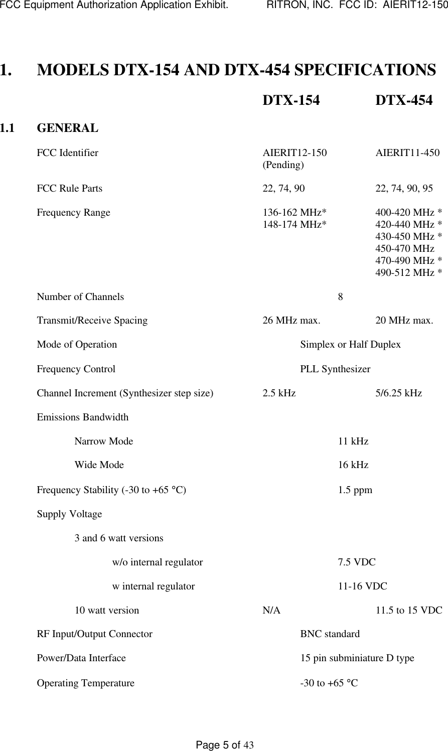
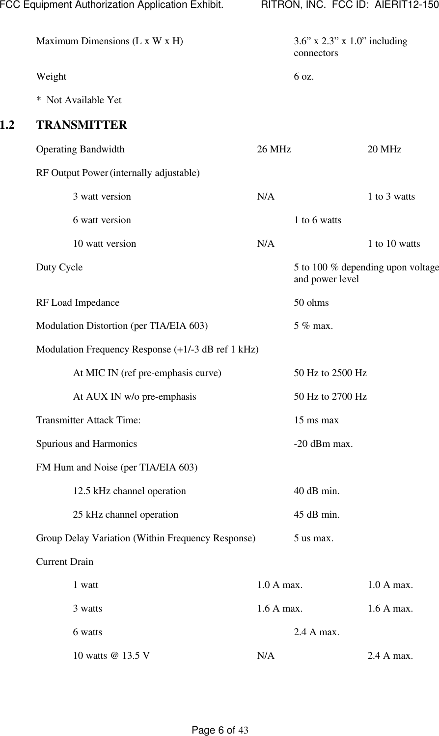
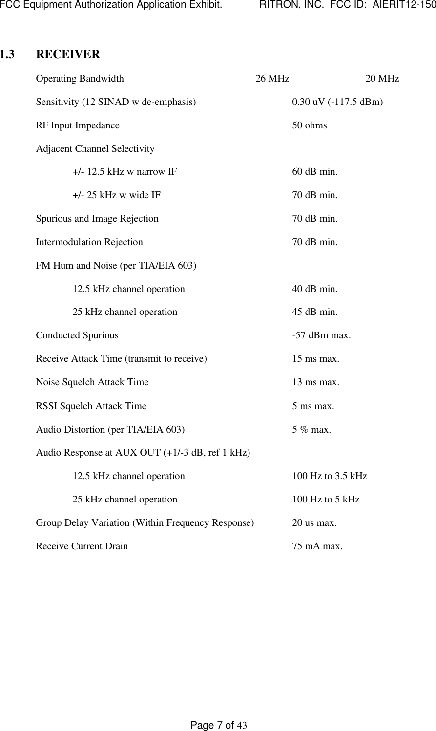
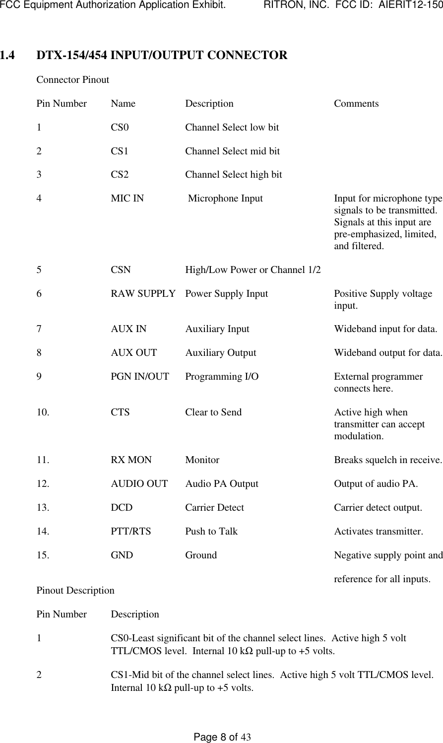
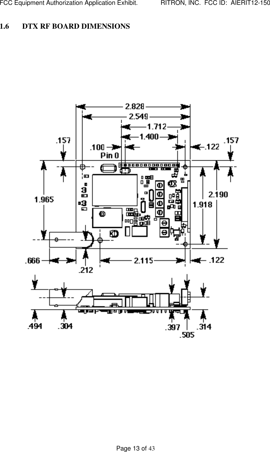
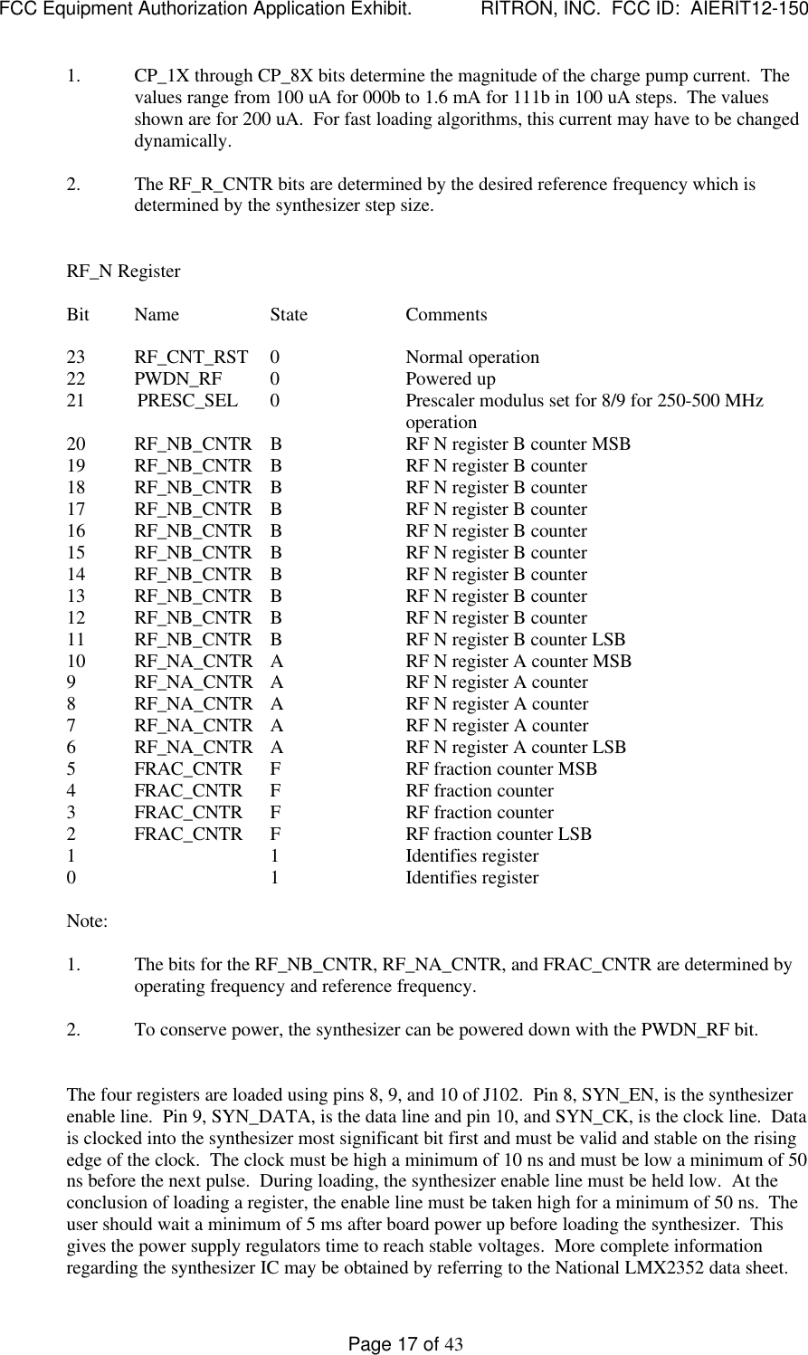
Ritron RIT12-150 Voice/Data Tranceiver Module User Manual DTX 150 FCC Instruction Manual

Ritron Inc Voice/Data Tranceiver Module DTX 150 FCC Instruction Manual

Instruction Manual

FCC Equipment Authorization Application Exhibit.             RITRON, INC.  FCC ID:  AIERIT12-150Page 1 of 43TYPE OF EXHIBIT:INSTRUCTION BOOK (PRELIMINARY)FCC PART:2.983 (d) (8)MANUFACTURER:RITRON, INC.505 West Carmel DriveCarmel, IN 46032MODEL:DTX-154TYPE OF UNIT:UHF-FM TransceiverFCC ID: AIERIT12-150DATE: September 15, 1999Preliminary Instruction Book follows.
FCC Equipment Authorization Application Exhibit.             RITRON, INC.  FCC ID:  AIERIT12-150Page 2 of 43RITRON, INC.                         PRELIMINARY 08-99RITRON MODELS DTX-154 & DTX-454PROGRAMMABLEFM TRANSCEIVER MODULESMAINTENANCE & OPERATINGMANUALFOR USE ONLY BY AUTHORIZED SERVICE/MAINTENANCE PERSONNEL
FCC Equipment Authorization Application Exhibit.             RITRON, INC.  FCC ID:  AIERIT12-150Page 3 of 43IMPORTANT MAINTENANCE/REPAIR INFORMATIONSurface Mount Repair:  RITRON surface mount products require special equipment and servicingtechniques.  Improper servicing techniques can cause permanent damage to the printed circuit board and/orcomponents, which is not covered by RITRON’s warranty.  If you are not completely familiar with surfacemount component repair techniques, RITRON recommends that you defer maintenance to qualified servicepersonnel.Precautions For Handling CMOS Devices: The DTX transceiver module contains complementary metal-oxide semiconductor (CMOS) devices, which require special handling techniques.  CMOS circuits aresusceptible to damage by electrostatic or high voltage charges.  Damage can be latent, with no failureappearing until weeks or months later.  For this reason, take special precautions any time you disassemblethe module.  Follow the precautions below, which are even more critical in low humidity environments.1) Storage/transport-CMOS devices that will be stored or transported must be placed in conductivematerial so that all exposed leads are shorted together.  CMOS devices must not be inserted intoconventional plastic “snow” or plastic trays of the type that are being used for other semiconductors.Conductive containers are typically gray or pink in color.2) Grounding-All CMOS devices must be placed on a grounded bench surface.  The technician that willwork on the radio/CMOS circuit must be grounded before handling the radio.  Normally, thetechnician wears a conductive wrist strap in series with a 100 kΩ resistor to ground.3) Clothing-Do not wear nylon clothing while handling CMOS circuits.4) Power Off-Remove power before connecting, removing, or soldering on a PC board that containsCMOS devices.5) Power/Voltage Transients-Do not insert or remove CMOS devices with power applied.  Check allpower supplies to be used for testing CMOS devices, making sure that no voltage transients arepresent.6) Soldering-Use a soldering iron with a grounded tip for soldering CMOS circuitry.7) Lead-Straightening Tools-When straightening CMOS leads, provide ground straps for the tool used.VCO Shield: The VCO shield is virtually impossible to remove without damaging either the PC board ornearby components.  The parts within the shield are low failure items; repair or replacement should not berequired unless the RF board is mishandled.  If failure of a part within the shield is deemed to haveoccurred, the RF board should be returned to RITRON for service or replacement.Unit Disassembly and Re-assembly:1) Case Removala) Remove the two screws at the rear of the unit.  These screws secure the rear bracket to thecase.b) Remove the two screws (one per side) on the side of the unit.  These screws secure the frontbracket to the case.c) Slide the case off the two-board assembly.2) Board Separation
FCC Equipment Authorization Application Exhibit.             RITRON, INC.  FCC ID:  AIERIT12-150Page 4 of 43Remove the two screws that secure the Loader Board to the rear bracket.  Remove the two screws thatsecure the RF board to the front bracket.  The two boards are held together by their interconnectingheader/socket.  Gently pry the two boards apart at the header/socket.  The RF board is then rotated andtilted so to allow the right angle BNC connector to pass through the hole in the front bracket.3) Re-assembly is the reverse of assembly with the rear screws installed before the side screws.
FCC Equipment Authorization Application Exhibit.             RITRON, INC.  FCC ID:  AIERIT12-150Page 5 of 431. MODELS DTX-154 AND DTX-454 SPECIFICATIONSDTX-154 DTX-4541.1 GENERALFCC Identifier AIERIT12-150 AIERIT11-450(Pending)FCC Rule Parts 22, 74, 90 22, 74, 90, 95Frequency Range 136-162 MHz* 400-420 MHz *148-174 MHz* 420-440 MHz *430-450 MHz *450-470 MHz470-490 MHz *490-512 MHz *Number of Channels 8Transmit/Receive Spacing 26 MHz max. 20 MHz max.Mode of Operation Simplex or Half DuplexFrequency Control PLL SynthesizerChannel Increment (Synthesizer step size) 2.5 kHz 5/6.25 kHzEmissions BandwidthNarrow Mode 11 kHzWide Mode 16 kHzFrequency Stability (-30 to +65 °C) 1.5 ppmSupply Voltage3 and 6 watt versionsw/o internal regulator 7.5 VDCw internal regulator 11-16 VDC10 watt version N/A 11.5 to 15 VDCRF Input/Output Connector BNC standardPower/Data Interface 15 pin subminiature D typeOperating Temperature -30 to +65 °C
FCC Equipment Authorization Application Exhibit.             RITRON, INC.  FCC ID:  AIERIT12-150Page 6 of 43Maximum Dimensions (L x W x H) 3.6” x 2.3” x 1.0” includingconnectorsWeight 6 oz.*  Not Available Yet1.2 TRANSMITTEROperating Bandwidth 26 MHz 20 MHzRF Output Power(internally adjustable)3 watt version N/A 1 to 3 watts6 watt version 1 to 6 watts10 watt version N/A 1 to 10 wattsDuty Cycle 5 to 100 % depending upon voltageand power levelRF Load Impedance 50 ohmsModulation Distortion (per TIA/EIA 603) 5 % max.Modulation Frequency Response (+1/-3 dB ref 1 kHz)At MIC IN (ref pre-emphasis curve) 50 Hz to 2500 HzAt AUX IN w/o pre-emphasis 50 Hz to 2700 HzTransmitter Attack Time: 15 ms maxSpurious and Harmonics -20 dBm max.FM Hum and Noise (per TIA/EIA 603)12.5 kHz channel operation 40 dB min.25 kHz channel operation 45 dB min.Group Delay Variation (Within Frequency Response) 5 us max.Current Drain1 watt 1.0 A max. 1.0 A max.3 watts 1.6 A max. 1.6 A max.6 watts 2.4 A max.10 watts @ 13.5 V N/A 2.4 A max.
FCC Equipment Authorization Application Exhibit.             RITRON, INC.  FCC ID:  AIERIT12-150Page 7 of 431.3 RECEIVEROperating Bandwidth 26 MHz 20 MHzSensitivity (12 SINAD w de-emphasis) 0.30 uV (-117.5 dBm)RF Input Impedance 50 ohmsAdjacent Channel Selectivity+/- 12.5 kHz w narrow IF 60 dB min.+/- 25 kHz w wide IF 70 dB min.Spurious and Image Rejection 70 dB min.Intermodulation Rejection 70 dB min.FM Hum and Noise (per TIA/EIA 603)12.5 kHz channel operation 40 dB min.25 kHz channel operation 45 dB min.Conducted Spurious -57 dBm max.Receive Attack Time (transmit to receive) 15 ms max.Noise Squelch Attack Time 13 ms max.RSSI Squelch Attack Time 5 ms max.Audio Distortion (per TIA/EIA 603) 5 % max.Audio Response at AUX OUT (+1/-3 dB, ref 1 kHz)12.5 kHz channel operation 100 Hz to 3.5 kHz25 kHz channel operation 100 Hz to 5 kHzGroup Delay Variation (Within Frequency Response) 20 us max.Receive Current Drain 75 mA max.
FCC Equipment Authorization Application Exhibit.             RITRON, INC.  FCC ID:  AIERIT12-150Page 8 of 431.4 DTX-154/454 INPUT/OUTPUT CONNECTORConnector PinoutPin Number Name Description Comments1CS0 Channel Select low bit2CS1 Channel Select mid bit3CS2 Channel Select high bit4MIC IN  Microphone Input Input for microphone typesignals to be transmitted.Signals at this input arepre-emphasized, limited,and filtered.5CSN High/Low Power or Channel 1/26RAW SUPPLY Power Supply Input Positive Supply voltageinput.7AUX IN Auxiliary Input Wideband input for data.8AUX OUT Auxiliary Output Wideband output for data.9PGN IN/OUT Programming I/O External programmerconnects here.10. CTS Clear to Send Active high whentransmitter can acceptmodulation.11. RX MON Monitor Breaks squelch in receive.12. AUDIO OUT Audio PA Output Output of audio PA.13. DCD Carrier Detect Carrier detect output.14. PTT/RTS Push to Talk Activates transmitter.15. GND Ground Negative supply point andreference for all inputs.Pinout DescriptionPin Number Description1CS0-Least significant bit of the channel select lines.  Active high 5 voltTTL/CMOS level.  Internal 10 kΩ pull-up to +5 volts.2CS1-Mid bit of the channel select lines.  Active high 5 volt TTL/CMOS level.Internal 10 kΩ pull-up to +5 volts.
FCC Equipment Authorization Application Exhibit.             RITRON, INC.  FCC ID:  AIERIT12-150Page 9 of 433CS2-Most significant bit of the channel select lines.  Active high 5 voltTTL/CMOS level.  Internal 10 kΩ pull-up to +5 volts.Channel CS2 CS1 CS01 0 0 02 0 0 13 0 1 04 0 1 15 1 0 06 1 0 17 1 1 08 1 1 10 = Logic low1 = Logic highNote:  Due to the internal pull-up resistors, the unit defaults to channel 8 if thechannel pins are left open (unconnected).4MIC IN-Microphone input.  This input accepts microphone type input signalsfor transmit. The signal is amplified, passed through the clipper and the clipperfilter and then to the RF board.  This input can be programmed to be disabled(muted) if desired.5CSN-When enabled through programming, this input selects between channels 1and 2.  This input is TTL/CMOS level type input with a logic low required forchannel 1 and a logic high required for channel 2.  Internal 10 kΩ pull-up to +5volts.6RAW SUPPLY- The positive supply voltage for the unit is supplied through thispin.  The actual supply voltage required depends upon model type.  Ensure thatthe correct supply voltage per the given model is used.7AUX IN-This is the broadband input for modulation.  The gain through thisinput to the modulator is programmable, as is the use of pre-emphasis.  Thissignal passes the clipper and clipper filter.8AUX OUT-This is the broadband output of the receiver.  The gain from thereceiver to the output is programmable, as is the use of de-emphasis.  The choiceof AC or DC coupling from the RF board discriminator is also programmable.The coupling at the output of this pin is AC coupled, however.  It can beconverted to DC coupling with internal hardware modifications.9PGN IN/OUT-Connect via RITRON RPT-PCPK PC Programming Kit tocomputer for programming the unit.10 CTS-Clear-To-Send output from the unit which indicates that the unit istransmitting a carrier at the correct frequency and power level and is ready toaccept an input signal to be transmitted.  This output would normally becometrue in response to a PTT RTS (see pin 14 description below) activation.  Thepolarity of this output can be programmed.  The output is active low 5 volt logicwith an internal 10 k ohm pull-up to 5 volts.  It can source up to 10 mA whenlow.
FCC Equipment Authorization Application Exhibit.             RITRON, INC.  FCC ID:  AIERIT12-150Page 10 of 4311 RX MON-This input breaks the squelch on the receiver i.e. allows formonitoring the channel even when a signal not strong enough to break squelch ispresent.  Input levels are TTL/CMOS; polarity may be programmed.  Internal 10kΩ pull-up to +5 volts.12 AUDIO OUT-This is the output of the audio power amplifier.  This output candrive up to ½ watt in to an 8 ohm load.  This output can be enabled and its gaincontrolled by programming.13 DCD-Carrier detect output.  This output becomes true when a signal strongenough to exceed the programmed squelch threshold is present.  This output isnot affected by the RX MON input.  The polarity can be programmed.  Theoutput is active low 5 volt logic with an internal 10 kΩ pull-up to +5 volts.  Itcan source up to 10 mA when low.14 PTT/RTS-Push to Talk/Request to Send.  This input commands the unit totransmit.  Input levels are TTL/CMOS; polarity may be programmed.  Internal10 kΩ pull-up to +5 volts.15 GND-System ground.  All signals and voltages are referenced to this input.  Thenegative side of the power supply should connect here.1.5 RF BOARD J301 INPUT/OUTPUTPin Number Name DescriptionJ102-0 PWR_SET When PC board jumper R185 is installed (R186 omitted), thevoltage on this pin controls the RF output power.  When R186is installed (R185 omitted), the RF output power is controlledby R187 on the RF board and this pin has no function.  Whenthis pin is used, the voltage should range between about 1 and4.5 VDC to vary the output power from 1 to 5 watts.  Therelationship between output power and voltage is non-linearand may vary as a function of operating frequency.  The inputresistance at this pin is approximately 15 k-ohm.J101-1 GND System ground.  All voltages are referenced to this point.J101-2                  FB+ Power supply input for the RF PA module.  Voltage at this pinis filtered.  Current drain can be as high as 2.5 amperes at 5watts RF output.J102-3 TX_EN Active high, 5 volt CMOS logic level input used to enable thetransmitter driver stage and PA pin diodes.  Timing circuitryexists on the RF board to ramp the PA power up or down tocontrol keying spurious outputs.J102-4                 RX_EN Active high, 5 volt CMOS logic level input used to enable thereceiver stages and to set the VCO to the receive frequencyrange.J102-5                 XCVR_EN Active high, 5 volt logic level input used to enable all stagesof the board except the PA and PA driver stages.  This pin can
FCC Equipment Authorization Application Exhibit.             RITRON, INC.  FCC ID:  AIERIT12-150Page 11 of 43be used to conserve current consumption in a battery saveconfiguration.J102-6                 MOD_IN Modulation input for the transmitter.  The modulating signalmust be superimposed upon a very stable and low noise 2.5VDC level.  Modulation sensitivity is approximately 14kHz/V.  The input resistance is approximately 17 k-ohm.Note:  The DC voltage at this pin directly controls thefrequency of the unit.  Therefore, the DC voltage must be wellregulated and controlled over environmental conditions.J102-7                 LOCK_DETECT Lock detect output of the frequency synthesizer.  Output is at5 volt logic level with a low level indicating lock.J102-8                 SYN_EN Enable line for loading the synthesizer.  Signal is at 5 voltCMOS logic levels.J102-9                 SYN_DATA Data line for loading the synthesizer.  Signal is at 5 voltCMOS logic levels.J102-10                SYN_CK Clock line for loading the synthesizer.  Signal is at 5 voltCMOS logic levels.J102-11                +7.2V +7.2 VDC +/- 10 % input for powering all stages of the radioexcept the RF PA module.  Current drain is approximately 45mA in receive and 100 mA in transmit.J102-12                RSSI Receive signal strength indicator output.  This is a highimpedance output, which is used to indicate the presence of acarrier.  When R124 is installed (R125 omitted), the outputwill vary between approximately 0.5 VDC and 3.0 VDC as theinput signal level varies between –130 dBm and –70 dBm.When R125 is installed (R124 omitted), the output will varybetween approximately 2.5 VDC at 0 dB SINAD to 0.5 VDCat 20 dB SINAD.  The loading on this outputmust be kept above 100 k-ohm.J102-13                DISC_OUT DC coupled discriminator output.  The polarity of this outputis controlled by R131 and R132.  For positive polarity i.e. anincrease in carrier frequency causes the DC level to increase,R131 should be installed and R132 omitted.  For negativepolarity, R132 should be installed and R1431 omitted.  Theoutput is low impedance with a modulation sensitivity ofapproximately 0.5 V/kHz for narrow band units and 0.25V/kHz for wide band units.  The DC level at this pin  istypically between 2 and 4 volts.J102-14                VCO_MOD When R179 is installed (R178 omitted), a signal at this pinwill modulate the VCO.  When R178 is installed (R179omitted), the VCO receives its modulation from the MOD_INpin and this pin has no function.  This pin is provided to allowthe modulation balance to be controlled through an externalboard rather than R180 on the RF board.  If this pin is to beused, the DC level should be approximately 5 VDC and froma low noise source.  The DC voltage at this pin does not affect
FCC Equipment Authorization Application Exhibit.             RITRON, INC.  FCC ID:  AIERIT12-150Page 12 of 43the transmit frequency.  The modulation sensitivity isapproximately 20 kHz/V.Note: An RF board purchased as a stand-alone board has components installed to support easyinterface to external circuitry.  This includes, but is not limited to, potentiometers forsetting deviation and balance, and various zero ohm jumpers.  If the zero ohm jumpersare placed in the correct position, operation with the RITRON loader board is possible.An RF board which is part of a DTX module cannot as easily be integrated in a system asa stand-alone board since the parts not required when used with the RITRON loaderboard are not installed.
FCC Equipment Authorization Application Exhibit.             RITRON, INC.  FCC ID:  AIERIT12-150Page 13 of 431.6 DTX RF BOARD DIMENSIONS
FCC Equipment Authorization Application Exhibit.             RITRON, INC.  FCC ID:  AIERIT12-150Page 14 of 431.7 DTX SYNTHESIZER PROGRAMMINGThe following information describes the DTX-154/454 synthesizer programming format.  Thisinformation can be used for designing programming software for the DTX-154/454 RF boardsynthesizer when the DTX-154/454 Loader board is not used.Note:  The user must obtain FCC Type Acceptance when the RITRON RF board is notused with the RITRON Loader board in the DTX-154/454 enclosure.The DTX-154/454 RF board uses a PLL (Phase Locked Loop) frequency synthesizer whichcompares the phase of the outputs of two digital frequency dividers.  One divider divides the VCO(Voltage Controlled Oscillator) frequency and the other divides the reference frequency.  If thetwo divided outputs differ in frequency, an error signal is generated which, after filtering, is usedto control the frequency of the VCO.  The net result is that the VCO is locked in frequency to aninteger multiple of the reference.  To set the desired frequency, the divider values must bedetermined.  These values are converted to binary and become part of four control words, whichmust be loaded into the synthesizer IC for proper operation.  The steps for determining thefrequency control part of the words is as follows:1. The RF R register counter value is first determined.  This integer is the referenceoscillator frequency (14.4 MHz in this product) divided by desired reference frequency.The reference frequency is 16 times the desired synthesizer step size.  Typical step sizesare 2.5 kHz for VHF and either 5 kHz or 6.25 kHz for UHF.  For a 6.25 kHz step size anda 14.4 MHz reference oscillator, the R register counter value would be 144 decimal.When converted to binary, this value is substituted for the R in the State column in theRF_R_Register table.2. The RF N register counter values are then determined.  This is accomplished by takingthe desired VCO frequency and dividing it by the desired synthesizer step size value usedabove.  The resulting integer is converted to binary.  The least significant 4 bits becomethe value for the FRAC_CNTR.  For frequencies below 500 MHz, bit 21 (PRESC_SEL)must be set to 0 with the next 3 significant bits of the integer used to fill in the 3 leastsignificant bits of RF_NA_CNTR (bits 6,7,and 8).  The two most significant bits ofRF_NA_CNTR (bits 9 and 10) are loaded with 0.  The remaining bits of the integer areloaded into RF_NB_CNTR (bits 11 through 20).  For frequencies above 500 MHz, bit 21(PRESC_SEL) must be set to 1 and the 4 bits following the 3 loaded into FRAC_CNTRare used for RF_NA_CNTR with the most significant bit of RF_NA_CNTR (bit 10) setto 0.  The remaining bits of the integer are loaded into RF_NB_CNTR.3. In transmit, the VCO frequency is equal to the operating frequency.  In receive, the VHFunits have a VCO frequency which is 43.650 MHz above the receive frequency.  TheVCO in the UHF units operate 43.650 MHz below the desired receive frequency.  Whencalculating receive values, ensure that 43.650 MHz is either added or subtracted(depending upon whether the unit is VHF or UHF) from the desired frequency beforebeginning the above calculations.  4. Example:For a frequency of 461.750 MHz in transmit with a 6.25 kHz step size, the RF_R value is144 decimal or  0000 0000 1001 0000 binary.  The RF_R register would thereforebecome 1000 0110 0000 0010 0100 0010 (MSB first).  The VCO frequency divided bythe step size is 73,880 decimal or  0001 0010 0000 1001 1000 binary.  The RF_N registerwould therefore become 0001 0010 0000 1000 0110 0011 binary.  For 461.750 MHzreceive, the VCO frequency would be 418.100 MHz (461.750 – 43.650) which yields a
FCC Equipment Authorization Application Exhibit.             RITRON, INC.  FCC ID:  AIERIT12-150Page 15 of 43divider of 66,896 decimal or 0001 0000 0101 0101 0000 binary.  The RF_N registerwould become 0001 0000 0101 0001 0100 0011 binary.The four registers of the synthesizer, their bit definitions, and required states are shown below:IF-R RegisterBit Name State Comments23 OSC 0External reference oscillator22 FRAC 16 1Fraction = 1621 FoLD 0RF digital lock detect20 FoLD 1RF digital lock detect19 FoLD 0RF digital lock detect18 CP_GAIN_8 XDon’t care (1=IF charge pump current=8X)17 IF_PD_POL XDon’t care (1=positive polarity on IF charge pump)16 IF_R_CNTR XDon’t care (IF reference divider MSB)15 IF_R_CNTR XDon’t care14 IF_R_CNTR XDon’t care13 IF_R_CNTR XDon’t care12 IF_R_CNTR XDon’t care11 IF_R_CNTR XDon’t care10 IF_R_CNTR XDon’t care9IF_R_CNTR XDon’t care8IF_R_CNTR XDon’t care7IF_R_CNTR XDon’t care6IF_R_CNTR XDon’t care5IF_R_CNTR XDon’t care4IF_R_CNTR XDon’t care3IF_R_CNTR XDon’t care2IF_R_CNTR XDon’t care (IF reference divider LSB)1 0Identifies register0 0 Identifies registerNotes:1. The IF part of the dual synthesizer is not used.  Only those bits which affect the RF partof the synthesizer have importance.IF_N RegisterBit Name State Comments23 IF_CNT_RS 0Normal operation22 PWDN_IF 1IF powered down21 PWDN_MODE 0Asynchronous power down20 Fastlock 1Fastlock enabled19 Test 0Test bit-should be set to 018 OUT_1 XDon’t care in fastlock mode17 OUT-0 XDon’t care in fastlock mode
FCC Equipment Authorization Application Exhibit.             RITRON, INC.  FCC ID:  AIERIT12-150Page 16 of 4316 IF_NB_CNTR XDon’t care (IF N register B counter MSB)15 IF_NB_CNTR XDon’t care14 IF_NB_CNTR XDon’t care13 IF_NB_CNTR XDon’t care12 IF_NB_CNTR XDon’t care11 IF_NB_CNTR XDon’t care10 IF_NB_CNTR XDon’t care9IF_NB_CNTR XDon’t care8IF_NB_CNTR XDon’t care7IF_NB_CNTR XDon’t care6IF_NB_CNTR XDon’t care5IF_NB_CNTR XDon’t care (IF N register B counter LSB)4IF_NA_CNTR XDon’t care (IF N register A counter MSB)3IF_NA_CNTR XDon’t care2IF_NA_CNTR XDon’t care (IF N register A counter LSB)1 0 Identifies register0 1 Identifies registerNote:1. The IF part of the dual synthesizer is not used.  Only those bits which affect the RFportion of the synthesizer and the bits to shut down the IF portion are used.RF_R RegisterBit Name State Comments23 DLL_MODE 1Delay line loop calibration enabled22 V2_EN 0Charge pump voltage doubler not enabled21 CP_8X 0Charge pump current MSB20 CP_4X 0Charge pump current MSB-119 CP_2X 0Charge pump current LSB+118 CP_1X 1Charge pump current LSB17 PF_PD_PO 1Charge pump polarity is positive16 RF_R_CNTR RRF R register counter MSB15 RF_R_CNTR RRF R register counter14 RF_R_CNTR RRF R register counter13 RF_R_CNTR RRF R register counter12 RF_R_CNTR RRF R register counter11 RF_R_CNTR  RRF R register counter10 RF_R_CNTR RRF R register counter9RF_R_CNTR RRF R register counter8RF_R_CNTR RRF R register counter7RF_R_CNTR RRF R register counter6RF_R_CNTR RRF R register counter5RF_R_CNTR RRF R register counter4RF_R_CNTR RRF R register counter3RF_R_CNTR RRF R register counter2RF_R_CNTR RRF R register counter LSB1 1 Identifies register0 0 Identifies registerNotes:
FCC Equipment Authorization Application Exhibit.             RITRON, INC.  FCC ID:  AIERIT12-150Page 17 of 431. CP_1X through CP_8X bits determine the magnitude of the charge pump current.  Thevalues range from 100 uA for 000b to 1.6 mA for 111b in 100 uA steps.  The valuesshown are for 200 uA.  For fast loading algorithms, this current may have to be changeddynamically.2. The RF_R_CNTR bits are determined by the desired reference frequency which isdetermined by the synthesizer step size.RF_N RegisterBit Name State Comments23 RF_CNT_RST 0Normal operation22 PWDN_RF 0Powered up21           PRESC_SEL 0Prescaler modulus set for 8/9 for 250-500 MHzoperation20 RF_NB_CNTR BRF N register B counter MSB19 RF_NB_CNTR BRF N register B counter18 RF_NB_CNTR BRF N register B counter17 RF_NB_CNTR BRF N register B counter16 RF_NB_CNTR BRF N register B counter15 RF_NB_CNTR BRF N register B counter14 RF_NB_CNTR BRF N register B counter13 RF_NB_CNTR BRF N register B counter12 RF_NB_CNTR BRF N register B counter11 RF_NB_CNTR BRF N register B counter LSB10 RF_NA_CNTR ARF N register A counter MSB9RF_NA_CNTR ARF N register A counter8RF_NA_CNTR ARF N register A counter7RF_NA_CNTR ARF N register A counter6RF_NA_CNTR ARF N register A counter LSB5FRAC_CNTR FRF fraction counter MSB4FRAC_CNTR FRF fraction counter3FRAC_CNTR FRF fraction counter2FRAC_CNTR FRF fraction counter LSB1 1 Identifies register0 1 Identifies registerNote:1. The bits for the RF_NB_CNTR, RF_NA_CNTR, and FRAC_CNTR are determined byoperating frequency and reference frequency.2. To conserve power, the synthesizer can be powered down with the PWDN_RF bit.The four registers are loaded using pins 8, 9, and 10 of J102.  Pin 8, SYN_EN, is the synthesizerenable line.  Pin 9, SYN_DATA, is the data line and pin 10, and SYN_CK, is the clock line.  Datais clocked into the synthesizer most significant bit first and must be valid and stable on the risingedge of the clock.  The clock must be high a minimum of 10 ns and must be low a minimum of 50ns before the next pulse.  During loading, the synthesizer enable line must be held low.  At theconclusion of loading a register, the enable line must be taken high for a minimum of 50 ns.  Theuser should wait a minimum of 5 ms after board power up before loading the synthesizer.  Thisgives the power supply regulators time to reach stable voltages.  More complete informationregarding the synthesizer IC may be obtained by referring to the National LMX2352 data sheet.
FCC Equipment Authorization Application Exhibit.             RITRON, INC.  FCC ID:  AIERIT12-150Page 18 of 432.0 INTRODUCTION2.1 GENERALThe RITRON DTX-154/454 modules are programmable 2-way radios, which operates either inthe VHF or UHF professional FM communications bands.  Each of eight channels can beprogrammed to contain a unique set of operating frequencies.  The DTX-154/454 module is madeup of two PC boards, an RF board and a Loader/Control board.  These two boards are enclosed ina metal case with two connectors on one end; a 50 ohm BNC connector for connection to anantenna and a DB-15 sub-miniature connector for power and control input/output.In addition, the RF board is available as a stand-alone unit for system integrators.  The RF boardas sold as a stand-alone item has a few more hardware options than when installed and sold as partof a module.  See section 7 for details on the hardware options.3. MODEL IDENTIFICATIONThe part number system for the DTX-154/454 module is as follows:The module has a part number in the form of  “DTX-A54-BCDEF”Where:A is the major frequency band designator:1=VHF4=UHFB is the sub-band designator:G=136-162 for VHF and 400-420 for UHFA=420-440B=430-450O=148-174 for VHF and 450-470 for UHFC=470-490T=490-512C is the connector designator:B=BNC connectorD designates the IF bandwidth:N=narrowW=wideE designates the maximum power level:3=3 watts6=6 watts9=10 wattsF designates whether the loader board has a regulator and if so, at what current level:
FCC Equipment Authorization Application Exhibit.             RITRON, INC.  FCC ID:  AIERIT12-150Page 19 of 43D=no regulator; the unit must operate at +7.5 VDC and is limited to either 3 or 6 wattsmax.L=low current regulator; the power module is not regulated.  Used for 10 watt versiononly.I=high current regulator; the unit operates from 10-15 volts at either 3 or 6 watts max.Example:  A DTX-454-OBN6I would be a UHF module for operation between 450 and 470 MHzwith a BNC RF connector, narrow (12.5 kHz channel spacing) IF bandwidth, 6 watts maximumoutput power, and an internal regulator to allow operation from 10 to 15 volts.The part number system for a stand-alone RF board is the same as that for a module except that“F” designator (regulator option) does not exist and a “-DD” is appended at the end.Note that the RF board inside a module is not exactly the same as the corresponding stand-aloneRF board.  There are a number of components and jumper options on the stand-alone board thatare not necessary when mated to the RITRON DTX loader/control board.2.3 FCC REGULATIONS2.3.1 LICENSINGThe FCC requires that the radio owner obtain a station license for his radio before using theequipment to transmit, but does not require an operating license or permit.  The station licensee isresponsible for proper operation and maintenance of his radio equipment, and for ensuring thattransmitter power, frequency and deviation are within the limits specified by the station license.This includes checking the transmitter frequency and deviation periodically using appropriatemethods.2.3.2 TYPE ACCEPTANCEThe unit is type accepted for transmission of either voice or data signals when aligned according tothe alignment procedure for the proper bandwidth and when operated as a complete unit in themetal case.  Operation of the RF board as a stand-alone unit or in combination with any otherequipment, in any mode outside the alignment procedure, or with the clipper filter electronicallydisabled will require the filing of a new type acceptance application with the FCC by the user.2.3.3 SAFETY STANDARDSThe FCC, with its action in General Docket 79-144, March 13, 1985, adopted a safety standard forhuman exposure to radio frequency electromagnetic energy emitted by FCC regulated equipment.RITRON follows these safety standards and recommends that you observe them also:DO NOT operate radio equipment near electrical blasting caps or in an explosive atmosphere.DO NOT operate any radio transmitter unless all RF connectors are secure and any openconnectors are properly terminated.DO NOT operate the transmitter of a fixed radio (base station, microwave, rural telephone RFequipment) or marine radio when someone is within two feet of the antenna.Repair of RITRON products should be performed only by RITRON authorized personnel.
FCC Equipment Authorization Application Exhibit.             RITRON, INC.  FCC ID:  AIERIT12-150Page 20 of 433.0 ACCESSORIESNote:  Programming kits are for use by authorized service/maintenance personnel only.The Programming Kit for DTX-154/454 radios (via compatible computer) is model RPT-PCKT.It includes:1) software installation instructions2) programming software diskettes, 3.5” and 5.25” (1 each)3) 1 PC/radio adapter cable (DB25F connector to 6 pin modular connector and to DB-15connector)Factory programming of channels and features is also optional.  Contact the factory for details.
FCC Equipment Authorization Application Exhibit.             RITRON, INC.  FCC ID:  AIERIT12-150Page 21 of 434.0 OPERATION4.1 CHANNEL SELECTIONThe DTX module supports eight channels.  The desired channel is chosen via pins 1,2, and 3 ofthe 15 pin connector as shown:Channel Pin 3 Pin 2 Pin 11 0 0 02 0 0 13 0 1 04 0 1 15 1 0 06 1 0 17 1 1 08 1 1 10 = Logic low1 = Logic highA logic low is a voltage level below 1 volt while a logic high is a voltage level above 3.5 volts.These three pins have an internal 10 kΩ pull-up resistor to + 5 volts.  Therefore, any pin leftunconnected will assume a logic high state.  Do NOT apply voltages outside the range of 0 to +5volts to these pins.A change in the channel selection in receive will cause the receiver to operate on the new channel.In transmit, however, the channel selection is only checked upon a push-to-talk activation.Changes in channel during transmit will not change the transmit operating channel of the unit untilthe unit is cycled from transmit to receive and back to transmit.4.2 POWER SUPPLY VOLTAGEPin 6 is the positive supply input to the unit.  The type of module determines the actual voltagethat should be applied to this pin.  One should be absolutely sure of the proper voltage and currentrequirements before applying power.Three voltages are used within the unit; +5 volts for the processor and logic circuits along withmost of the receiver, +7.5 volts for the transmitter driver stages, and the supply voltage for the RFpower module which depends upon which module is used.The VHF unit and the 3 and 6-watt UHF units use 7.5 volt RF power modules.  Two supplyvoltage options are available for these units depending upon whether the loader/control board hasa regulator installed.  If a regulator is not installed, the voltage should be 7.5 volts +/-10 %.  Thisvoltage should be “clean” and preferably regulated since the RF power module is powered directlyfrom this source.  Variations in voltage will cause variations in transmitted output power.Conversely, if the loader/control board has a regulator installed, the supply voltage can be at anyvoltage between 10 and about 15 volts.  Although the use of the regulator allows flexibility interms of supply voltage, because of the amount of heat generated by the regulator, significant dutycycle/key down limitations may apply (see below).
FCC Equipment Authorization Application Exhibit.             RITRON, INC.  FCC ID:  AIERIT12-150Page 22 of 43The RF power module in the 10 watt UHF unit requires at least 12 volts to achieve 10 watts,although voltages as high as 15 may be used.  Since the module is powered directly from thisvoltage, the supply should be “clean” and, preferably, regulated.  The output power will vary withsupply voltage.  The 7.5 volts required for the transmitter driver stages is developed by a regulator,but since the current requirements are limited, the regulator is not a factor in determining the dutycycle/key down limits.4.3 DUTY CYCLE/KEY-DOWN LIMITATIONS4.3.1 DTX MODULEThe major heat generating components within the module such as the RF power amplifier andvoltage regulator (if used) have maximum temperature limits that should not be exceeded.  Inaddition, the temperature within the module itself must be kept below the maximum temperatureof the reference oscillator.  As a result, depending upon power, supply voltage, and temperature,limits upon the average transmit duty cycle and the maximum continuous transmitter on timeexist.  These limits are summarized below for operation in still air:Temperature (°C)   Duty Cycle (%)   Key-Down Time (s)w/o internal regulator:3 watt RF output 25 100 3060 15 56 watt RF output 25 80 3060 10 510 watt RF output @ 13.5 V 25 30 1560 5 5w internal regulator3 watt RF output 25 50 2060 5 56 watt RF output 25 30 1560 5 5Blowing air across the unit and/or adding heat sinks can significantly improve the duty cycle/key-down times, especially in units without the internal regulator.4.3.2 RF BOARDIt is not possible to establish duty cycle/key-down limits for the stand-alone RF board since eachsystem in which the board is integrated is unique.  For those wishing to integrate the RF board intoa system, the RF PA module at the rear of the board is the only major source of heat generation.The rear-mounting bracket which holds the module should be bolted to a heat sink of some typewith a layer of thermal compound between them for good heat conduction.
FCC Equipment Authorization Application Exhibit.             RITRON, INC.  FCC ID:  AIERIT12-150Page 23 of 434.4 OPERATING MODES4.4.1 RECEIVECarrier Detect and Squelch OperationThe DTX is a transceiver; i.e. it can receive and transmit, although not at the same time.  A carrierdetect system exists within the unit to detect the presence of a carrier which controls the logic stateof the DCD (data carrier detect) output.  The RF levels at which this output changes state areprogrammable.  In addition, the unit may be programmed such that the audio outputs, AUDIOOUT and AUX OUT, are muted (squelched) in conjunction with DCD operation.  In units wheresquelch operation has been enabled, the RX MON input can be used to override a squelchedcondition.  The DCD output is not affected by the RX MON operation.Receiver Audio OutputsTwo receiver audio outputs are present on the DTX module.  The AUX OUT is general purposeoutput which can have pre-emphasis enabled or bypassed.  Its gain can be controlled and its outputis designed to drive 600 loads.  The coupling from the discriminator on the RF board may be set toAC or DC by the programmer.  The output stage is AC coupled, but can be modified for DCcoupling.  See the maintenance section of the manual for details on this modification.  TheAUDIO OUT is always de-emphasized, but its gain can be programmed.  In addition, transmitsidetone can be programmed as an option, if desired.  This output can drive 8 ohm speaker-typeloads.4.4.2 TRANSMITPTT OperationThe transmitter is activated by placing the PTT/RTS (Push-To-Talk/Request-To-Send) input in itstrue state.  This state is programmable.  If the unit is to operate in simplex (transmitter and receiveron the same frequency), one should check for activity on the channel before transmitting.  This canbe done by checking the state of the DCD output.  In addition, the unit can be programmed so thattransmit operation is inhibited if the DCD threshold has been exceeded.CTS OutputThe CTS (Clear To Send) output goes to its true state when the unit has powered up thetransmitter, is locked on the correct transmit frequency, and is ready to accept modulation.  Thisoutput may be used to signal a modem to start transmitting data.  If this output is not used, toavoid loosing data, a delay of at least 15 ms is required between PTT/RTS activation and theapplication of data.Transmitter Audio InputsTwo audio inputs are available on the DTX module.  The AUX IN is a general-purpose input thatcan have pre-emphasis enabled or bypassed and its gain can be controlled through programming.The input impedance is greater than 50 kΩ and is capacitive coupled with a lower roll-offfrequency of about 25 Hz.  The MIC IN input is fixed gain input designed for connection to astandard electret or dynamic microphone.  About 25 mV rms of input signal at 1 kHz will produce60 % of maximum deviation.  The signal at this input is pre-emphasized.  The signals at bothinputs pass through the modulation limiter and post-limiter filter.High/Low Power
FCC Equipment Authorization Application Exhibit.             RITRON, INC.  FCC ID:  AIERIT12-150Page 24 of 43If RNet compatibility mode is not programmed into the unit, high and low power levels can beprogrammed into the unit on a channel by channel basis.  High power is selected by placing theCSN input at a logic high state.  Placing the CSN input at a logic low state chooses low power.The CSN input has an internal pull-up resistor; it will assume the high state i.e. high power whenleft unconnected.Specialized Modem OperationModems designed to achieve the highest data rates possible in a radio channel may require a directDC connection to the modulation path and the removal of the limiter-filter.  In order to receiveFCC Type Acceptance, the DTX module must either be tested and approved with a specificmodem connected to the transmitter, or a modulation limiter and limiter-filter must always bepresent in the transmit modulator audio path with the modulation inputs AC coupled.  To allow forthe most flexibility for the end user, the unit was type accepted as a stand-alone unit.  It ispossible, with hardware modifications and special programming software (not supplied with theunit), to DC couple the AUX IN input and/or defeat the limiter-filter.  The modulation limiterwould still be in place, but the deviation of the DTX module could be set such that the modulationlimit within the DTX module is never reached.  The deviation would be set by the modem leveland the AUX IN gain setting.  The end user/system integrator would then bear the responsibility ofobtaining type acceptance or operating in a frequency band where type acceptance is not required.Contact RITRON for details.  Note:  Most modems will connect directly to the DTX withoutrequiring any special modifications or programming.Antenna PlacementThe DTX module is enclosed in a metal housing for RF shielding.  However, RF emitting sourceslocated very close (less than 12 inches) to the unit can at times affect its operation.  It is notrecommended that an antenna be connected directly to the module’s BNC connector unless the RFoutput power is set for less than 1 watt or the module is placed within another RF tight enclosure.4.5 RNET COMPATIBILITY MODEThe DTX module can be programmed to mimic some of the behavior of the RNet 450 radio.  Inthe RNet compatibility mode, the CSN input is used as a channel selector line.  A logic low selectschannel 1 while a logic high selects channel 2.  The channel select lines, CS0, CS1, and CS2 haveno effect.  Also, the DCD output is held in its true state during transmit.  It would normally befalse in transmit.
FCC Equipment Authorization Application Exhibit.             RITRON, INC.  FCC ID:  AIERIT12-150Page 25 of 435.0 PROGRAMMINGTo program the DTX Module, the RITRON PC Programming Kit must be used.5.1 PC PROGRAMMING KITThe RITRON adapter cable connects the radio to a computer’s serial communications port.  Oncethe cable is hooked up, the user inserts the diskette provided into the computer’s floppy disk driveand loads the programmer software.  This program transfers data between radio and computermemory and includes on-screen instruction.5.1.1 PROGRAMMING KIT CONTENTS AND REQUIREMENTSThe RITRON Programming Kit includes the following:1. Programming software that is contained on one diskette.2. Installation Instructions and a Registration Form.3. PC to radio adapter cable, which is terminated at one end with a DB-25F connector and at theother end with a modular plug.  The DB-25 connector plugs into the computer’s serial port,the modular plug into an adapter.4. The adapter for use with the DTX Plus series of radios.  This adapter mates the modular plugto a DB-15M plug for connection to the radio.The Programmer Kit requires a PC compatible computer with Windows 95 or later operatingsystem installed.  The computer must have an RS-232 serial port available.  A hard disk drive isrecommended.5.2 COMPUTER SOFTWARE COPYRIGHTSThe RITRON, Inc. products described in this manual include copyrighted RITRON, Inc. computerprograms.  Laws in the United States and other countries grant to RITRON, Inc. certain exclusiverights in its copyrighted computer programs, including the exclusive right to distribute copies ofthe programs, make reproductions of the programs, and prepare derivative works based on theprograms.  Accordingly, any computer programs contained in RITRON, Inc. products may not becopied or reproduced in any manner without the express written permission of RITRON, Inc.  Thepurchase of RITRON, Inc. products does not grant any license or rights under the copyrights orother intellectual property of RITRON, Inc. except for the non-exclusive, royalty fee license to usethat arises in the sale of a product, or as addressed in a written agreement between RITRON, Inc.and the purchaser of RITRON, Inc. products.
FCC Equipment Authorization Application Exhibit.             RITRON, INC.  FCC ID:  AIERIT12-150Page 26 of 435.3 PROGRAMMER MENUSThe DTX Programmer has four menus or pages, selectable via tabs at the top of each page, whichare always visible.  These pages are:1. Frequency Selection-Used to program the channel frequencies of the radio.2. Settings-Used to set programmable features/functions of the radio.3. Alignment-Used to align and set the internal digital potentiometers in the radio.  Informationon the use of this page is found in the Maintenance Manual.4. Summary-Used to summarize on one page the model, settings, and alignment information.5.3.1 FREQUENCY SELECTIONThe Frequency page has fields for each channel, transmit and receive for frequency information.Channel information can be entered by clicking on the appropriate box and entering the desiredfrequency.  The frequency chosen must be within the operating range of the radio and on afrequency that the synthesizer is capable of channeling i.e. for VHF, divisible by 2.5 kHz and forUHF, divisible by 5 or 6.25 kHz.  When the RNET compatibility mode is chosen, only channelone and two are available for programming.5.3.2 SETTINGSThe Settings page allows for programming various parameters of the radio.  These are detailedbelow:Microphone Mute-Allows the signal path from the MIC IN (microphone input) to be muted.  If themicrophone input is not to be used,  the “mute” function should be selected.TX Pre-emphasis-Allows for the signal path from AUX IN to be either pre-emphasized or flat.Most applications where the AUX IN input is used prefer a flat response.RX De-emphasis-Allows for the signal path from the discriminator to the AUX OUT to be eitherde-emphasized or flat.  Most applications where the AUX OUT output is used prefer a flatresponse.Busy Channel Lockout-Prevents the transmitter from activating when the carrier detect output istrue.  Used to prevent interference on a channel where activity already exists.  Not normallyenabled in half duplex operation since the transmit and receive channels are not on the samefrequency.Squelch Enable-Allows the receive audio paths to be muted when the carrier detect output is false.Used to prevent the output of noise from the audio outputs when no signal is present.  Due to thefinite squelch attack time, some high-speed modems prefer to work with unsquelched audio.DCD Output Logic Level-Allows the setting of the polarity of the DCD (Data Carrier Detect)output.  Active high means that the true state is a logic high while active low means that the truestate is logic low.  Normal setting is active high.Carrier Mode-Allows the programmer to set the radio to match the type of carrier detection usedby the RF board.  The carrier detect mode may be either RSSI (Receive Signal Strength Indicator),based upon carrier level or Noise, which is based upon the receive signal to noise level.  RSSIbased is significantly faster than noise based systems and is usually preferred for data applications
FCC Equipment Authorization Application Exhibit.             RITRON, INC.  FCC ID:  AIERIT12-150Page 27 of 43where fast turn-around times are important.  This selection must match that of the radiohardware.  It is preset at the factory to match the RF board and must not be changed unlessthe RF board is modified.  See the Maintenance Manual for details.Audio PA TX Sidetone-When enabled, the signal to be transmitted is made available at theAUDIO OUT output as a sidetone.CSN Input-Selects whether RNET Compatibility mode is to be used.  See section 4.5 for anexplanation of this function.  Normal operation is to set this for high/low Power.PTT/RTS Input Logic Level-Sets the polarity of the PTT/RTS input.  Normally set for active lowi.e. transmitter is activated when this input is at the logic low state.  Due to the internal pull-upresistor, setting this to active high will cause activation of the transmitter when the PTT/RTSinput is left unconnected.CTS Output Logic Level-Sets the polarity of the CTS (Clear-To-Send) output.  Setting for activehigh caused the true logic state to be high.  Active high is the normal setting.TX Timeout Timer-Allows for limits on the maximum time the transmitter may be keyedcontinuously.  When set, the maximum limit is set in the box.  To prevent overheating andpossible damage to the unit, this is normally set on with a time of 30 seconds.  See section 4.3.1for limits on maximum key-down times.5.3.3 SUMMARYThe summary page summarizes the information shown on the other three pages and, in addition,includes the model and serial number of the unit.
FCC Equipment Authorization Application Exhibit.             RITRON, INC.  FCC ID:  AIERIT12-150Page 28 of 436.0 THEORY OF OPERATION6.1 DTX-154 RF BOARD6.1.1 RECEIVERRF amplifier and Bandpass FiltersThe incoming RF signal from the input connector J101 passes backwards through the transmitterlowpass filter and the electronic T/R switch to a three pole bandpass filter formed around L102,L103, and L104.  This filter is of Cohn type with 1.5 dB insertion loss and a bandwidth of 30MHz.  This filter is followed by a low noise amplifier stage formed around Q101.  This amplifierhas a gain of about 17 dB with a noise figure of 2 dB and serves to amplify the incoming RFsignal above the noise of the following stages.  Following this stage is a three pole Cohn filterformed around L107 through L109.  The characteristics of this filter are identical to that of thefirst.  The two filter sections are narrow enough to filter out the spurious responses of the firstmixer while wide enough to support a performance bandwidth of 26 MHz.1st Mixer, 1st IF filters, and 1st IF AmplifierIC101 is an active double balanced mixer which converts the incoming RF signal to the firstintermediate frequency (IF) of 43.65 MHz.  This mixer has a gain of 0 dB and a noise figure of 10dB.  Its differential output is matched to the first IF filter, YF101, by L107, L108, C128, andC137.  An IF amplifier based around Q102 is used to provide gain.  Its output drives another IFfilter section, YF102, which is identical to YF101.  These two filters serve the double functionfiltering out the spurious responses of the second mixer and, with the second IF filter, of removingsignals at the adjacent and further removed channels.2nd IF ICThe output of YF102 drives the mixer internal to IC102.  IC102 is an integrated FM IF IC whichcontains a mixer, high gain limiting IF amplifier, FM discriminator (detector), and other supportcircuitry.  The mixer in IC102 converts the RF signal at the first IF to the second IF of 450 kHz.The output of the mixer exits the IC and is filtered by the second IF filter, YF103.  The output ofthe filter re-enters the IC and drives the high gain limiting amplifier.  Because the discriminatorinside IC102 is sensitive to both amplitude and frequency modulation components, a limiter mustprecede it to remove any amplitude modulation.  In addition, the noise based carrier detectionsystem available with this product requires that the RF signal at the discriminator stay constant inamplitude as the RF input signal level varies.  The output of the limiter amplifier drives thediscriminator.  The resonator for the discriminator is YF104.Receiver Audio and Carrier DetectionThe recovered audio from pin 9 of IC102 is filtered and DC shifted by IC103A and associatedcomponents.  IC103B is a simple inverter and is used to provide inverted audio for thoseapplications which may require it.Two methods of carrier detection are available on this radio.  One is based upon the absolute RFsignal level at IC102’s input and the other is based upon the magnitude of the ultrasonic noise onthe recovered audio.  IC102 has circuitry which develops a DC current which is proportional to theinput RF signal level.  Passing this current through a resistor (R115) creates a voltage which variesfrom about 0.5 volts at no signal input to about 3 volts with –70 dBm at the antenna connector.  Inaddition, a voltage can be developed which is proportional to the amount of noise present on therecovered audio signal.  This is effected by filtering the recovered audio such that only frequencies
FCC Equipment Authorization Application Exhibit.             RITRON, INC.  FCC ID:  AIERIT12-150Page 29 of 43above the normal modulation range remain.  This prevents modulation components from beingdetected as noise.  The filter is formed around an op-amp internal to IC102 between pins 10 and11 and the components connected to these two pins.  The filtered output at pin 11 is rectified byQ103B and then filtered.  The output varies from about 3 volts for a 0 dB SINAD signal to about0.5 volts for a 20 dB SINAD signal.2nd Local OscillatorThe two mixers in this radio act to produce an output signal whose frequency is equal to thedifference between the frequency present at the RF input port and the frequency at the localoscillator port.  To convert signals at the first IF frequency of 43.65 MHz to that of the second IFat a frequency of 450 kHz, a local oscillator signal at a frequency of 43.2 MHz (43.65 – 0.45) isused.  This signal is created by tripling the output of the radio’s 14.4 MHz master referenceoscillator, Y101.  Transistor Q111 acts as a frequency tripler.  Its associated components are usedto bias the transistor at an harmonic rich bias point and to filter the output such that only the thirdharmonic remains for use as the 2nd local oscillator.6.1.2 VCO AND SYNTHESIZERThe synthesizer is responsible for generating the carrier in transmit and the first local oscillator inreceive.  A voltage-controlled oscillator (VCO) is an oscillator whose frequency can be controlledby an external signal.  The synthesizer, almost wholly contained within IC108, divides the VCOfrequency by digital dividers and compares the result with an accurate reference.  An error signal,proportional to the frequency error is created which is routed to the frequency control input of theVCO.  This action locks the VCO to a frequency which is equal to the reference frequencymultiplied by the divider number.  To set the VCO frequency, different divider numbers can beprogrammed into the synthesizer.  In most synthesizer designs, the divider must be an integer,which forces the reference frequency to be equal to the synthesizer step size.  The synthesizer ICused in this radio, however, allows the use of non-integer values for the divider which in turnallows the reference frequency to be much higher than normal.  This creates a synthesizer whoseoutput has lower noise, lower spurious levels, and higher switching speeds.  The referencefrequency is derived by digitally dividing the frequency of the 14.4 MHz master oscillator.  Whenlocked, the VCO attains the same relative frequency stability as that of the master oscillator.The VCO itself is a voltage follower Hartley oscillator formed around Q107.  One of the elementsin the resonant circuit is a varactor diode, CR105, whose capacitance, when reverse biased, variesas a function of the applied voltage.  Since the oscillator frequency is controlled by the resonantcircuit, varying the voltage on the varactor diode effects a change in frequency.  To serve as alocal oscillator for the first mixer, the VCO operates at a frequency 43.65 MHz above that of thedesired receive frequency.  In receive, the VCO’s oscillating frequency range is shifted upward byabout 44 MHz by switching C191, C192, and L115 into the resonant circuit.  The VCO has atuning range of about 40 MHz when its tuning voltage is varied between 1 and 5 volts.  Tofrequency modulate the VCO for transmit, another varactor diode, CR106, is lightly coupled intothe resonant circuit.The output of the VCO is amplified to a level of about 0 dBm by  Q106.  Q110 with R171 andC196 act as a very low noise power supply filter for the VCO.6.1.3 TRANSMITTERPA Driver StagesThe output of the VCO buffer drives Q105 through R152.  The signal level at this point is about –10 dBm.  Q105 amplifies this signal to about +5 dBm.  Q104 further amplifies the signal to +13dBm, the level required by the PA module.  The supply voltage to these two stages is switched onin transmit by Q113.
FCC Equipment Authorization Application Exhibit.             RITRON, INC.  FCC ID:  AIERIT12-150Page 30 of 43PA Module, Lowpass Filter, and T/R SwitchWhen driven by +13 dBm, the PA module is capable of producing 6 watts or more of power at theantenna connector.  Pin 2 of the module is used for power control.  The output power level can bevaried from less than 0.5 watts to full power by changing the voltage at this pin.To reduce carrier frequency harmonics of the PA module output to acceptable levels, a lowpassfilter is inserted between the module and the antenna connector.  This filter is of elliptic design andformed around L115 and L116 and C169 through C173.To isolate the PA module from the receiver, an electronic T/R switch is used.  The switch isformed around PIN diodes CR103 and CR104 which are turned on in transmit and are off inreceive.  CR104 switches the PA module into and out of the circuit while CR103 protects andisolates the receiver input when the radio is in transmit.6.1.4 MISCELLANEOUS FUNCTIONSTwo on-board regulators are used to provide the 5 volts DC used by most of the circuitry in theradio.  IC107 is a low noise, low dropout regulator which provides 5 volts to all the portions of theradio which do not get switched on or off as the radio changes from transmit to receive.  Thisregulator is enabled by the XCVR-EN (J102, pin 5) input.  When this regulator is not enabled, theradio is essentially powered down.  IC108 is an identical regulator which supplies power to thosecircuits which are to be powered-up only in receive and to the switches in the VCO which shift theVCO frequency range to that needed in transmit.  The regulator is enabled through IC106E andIC106F by the RX-EN (J102, pin 4) input.The transmitter PA module driver stages and the T/R switch are powered by +7.2 volts throughQ113.  Q113 is enabled by the TX-EN (J102, pin3) input through delay and sequencing circuitryformed around IC106 and Q112 and Q114.  The sequencing circuitry delays PA turn-on until thedriver stages and T/R switches are on and delays driver stage and T/R switch shutdown until thePA module has ramped down in power.  This prevents “keyclicks” from abrupt transmitter turn-onand turn-off.
FCC Equipment Authorization Application Exhibit.             RITRON, INC.  FCC ID:  AIERIT12-150Page 31 of 436.2 DTX-454 RF BOARD6.2.1 RECEIVERRF Amplifier and Bandpass FiltersThe incoming RF signal from the input connector J101 passes backwards through the transmitterlowpass filter and the electronic T/R switch to a two pole bandpass filter formed around L101 andL102.  This filter is of Cohn type with 1.5 dB insertion loss and a bandwidth of 25 MHz.  Thisfilter is followed by a low noise amplifier stage formed around Q101.  This amplifier has a gain ofabout 17 dB with a noise figure of 2 dB and serves to amplify the incoming RF signal above thenoise of the following stages.  Following this stage is a four pole Cohn filter formed around L103through L106.  This filter has an insertion loss of 4 dB and a bandwidth of 25 MHz.  The two filtersections are narrow enough to filter out the spurious responses of the first mixer while wideenough to support a performance bandwidth of 20 MHz.1st mixer, 1st IF Filters, and 1st IF AmplifierIC101 is an active double balanced mixer which converts the incoming RF signal to the firstintermediate frequency (IF) of 43.65 MHz.  This mixer has a gain of 0 dB and a noise figure of 10dB.  Its differential output is matched to the first IF filter, YF101, by L107, L108, C128, andC137.  An IF amplifier based around Q102 is used to provide gain.  Its output drives another IFfilter section, YF102, which is identical to YF101.  These two filters serve the double functionfiltering out the spurious responses of the second mixer and, with the second IF filter, of removingsignals at the adjacent and further removed channels.2nd IF ICThe output of YF102 drives the mixer internal to IC102.  IC102 is an integrated FM IF IC whichcontains a mixer, high gain limiting IF amplifier, FM discriminator (detector), and other supportcircuitry.  The mixer in IC102 converts the RF signal at the first IF to the second IF of 450 kHz.The output of the mixer exits the IC and is filtered by the second IF filter, YF103.  The output ofthe filter re-enters the IC and drives the high gain limiting amplifier.  Because the discriminatorinside IC102 is sensitive to both amplitude and frequency modulation components, a limiter mustprecede it to remove any amplitude modulation.  In addition, the noise based carrier detectionsystem available with this product requires that the RF signal at the discriminator stay constant inamplitude as the RF input signal level varies.  The output of the limiter amplifier drives thediscriminator.  The resonator for the discriminator is YF104.Receiver Audio and Carrier DetectionThe recovered audio from pin 9 of IC102 is filtered and DC shifted by IC103A and associatedcomponents.  IC103B is a simple inverter and is used to provide inverted audio for thoseapplications which may require it.Two methods of carrier detection are available on this radio.  One is based upon the absolute RFsignal level at IC102’s input and the other is based upon the magnitude of the ultrasonic noise onthe recovered audio.  IC102 has circuitry which develops a DC current which is proportional to theinput RF signal level.  Passing this current through a resistor (R115) creates a voltage which variesfrom about 0.5 volts at no signal input to about 3 volts with –70 dBm at the antenna connector.  Inaddition, a voltage can be developed which is proportional to the amount of noise present on therecovered audio signal.  This is effected by filtering the recovered audio such that only frequenciesabove the normal modulation range remain.  This prevents modulation components from beingdetected as noise.  The filter is formed around an op-amp internal to IC102 between pins 10 and11 and the components connected to these two pins.  The filtered output at pin 11 is rectified by
FCC Equipment Authorization Application Exhibit.             RITRON, INC.  FCC ID:  AIERIT12-150Page 32 of 43Q103B and then filtered.  The output varies from about 3 volts for a 0 dB SINAD signal to about0.5 volts for a 20 dB SINAD signal.2nd Local OscillatorThe two mixers in this radio act to produce an output signal whose frequency is equal to thedifference between the frequency present at the RF input port and the frequency at the localoscillator port.  To convert signals at the first IF frequency of 43.65 MHz to that of the second IFat a frequency of 450 kHz, a local oscillator signal at a frequency of 43.2 MHz (43.65 – 0.45) isused.  This signal is created by tripling the output of the radio’s 14.4 MHz master referenceoscillator, Y101.  Transistor Q112 acts as a frequency tripler.  Its associated components are usedto bias the transistor at an harmonic rich bias point and to filter the output such that only the thirdharmonic remains for use as the 2nd local oscillator.6.2.2 VCO AND SYNTHESIZERThe synthesizer is responsible for generating the carrier in transmit and the first local oscillator inreceive.  A voltage-controlled oscillator (VCO) is an oscillator whose frequency can be controlledby an external signal.  The synthesizer, almost wholly contained within IC108, divides the VCOfrequency by digital dividers and compares the result with an accurate reference.  An error signal,proportional to the frequency error is created which is routed to the frequency control input of theVCO.  This action locks the VCO to a frequency which is equal to the reference frequencymultiplied by the divider number.  To set the VCO frequency, different divider numbers can beprogrammed into the synthesizer.  In most synthesizer designs, the divider must be an integer,which forces the reference frequency to be equal to the synthesizer step size.  The synthesizer ICused in this radio, however, allows the use of non-integer values for the divider which in turnallows the reference frequency to be much higher than normal.  This creates a synthesizer whoseoutput has lower noise, lower spurious levels, and higher switching speeds.  The referencefrequency is derived by digitally dividing the frequency of the 14.4 MHz master oscillator.  Whenlocked, the VCO attains the same relative frequency stability as that of the master oscillator.The VCO itself is a voltage follower Colpitts oscillator formed around Q108.  One of the elementsin the resonant circuit is a varactor diode, CR106, whose capacitance, when reverse biased, variesas a function of the applied voltage.  Since the oscillator frequency is controlled by the resonantcircuit, varying the voltage on the varactor diode effects a change in frequency.  To serve as alocal oscillator for the first mixer, the VCO operates at a frequency 43.65 MHz below that of thedesired receive frequency.  In transmit, the VCO’s oscillating frequency range is shifted upwardby about 44 MHz by switching C190 and L115 into the resonant circuit.  The VCO has a tuningrange of about 30 MHz when its tuning voltage is varied between 1 and 5 volts.  To frequencymodulate the VCO for transmit, another varactor diode, CR105, is lightly coupled into theresonant circuit.The output of the VCO is amplified to a level of about 0 dBm by Q107 and Q106.  Q111 withR172 and C196 act as a very low noise power supply filter for the VCO.6.2.3 TRANSMITTERPA Driver StagesThe output of the last VCO buffer drives Q105 through R151.  The signal level at this point isabout –10 dBm.  Q105 amplifies this signal to about +5 dBm.  Q104 further amplifies the signal to+17 dBm, the level required by the PA module.  The supply voltage to these two stages isswitched on in transmit by Q113.PA Module, Lowpass Filter, and T/R Switch
FCC Equipment Authorization Application Exhibit.             RITRON, INC.  FCC ID:  AIERIT12-150Page 33 of 43When driven by +17 dBm, the PA module is capable of producing 6 watts (10 watts in the 10 wattversion) or more of power at the antenna connector.  Pin 2 of the module is used for powercontrol.  The output power level can be varied from less than 0.5 watts to full power by changingthe voltage at this pin.To reduce carrier frequency harmonics of the PA module output to acceptable levels, a lowpassfilter is inserted between the module and the antenna connector.  This filter is of elliptic design andformed around a buried stripline transmission line and C164, C165, and C166.To isolate the PA module from the receiver, an electronic T/R switch is used.  The switch isformed around PIN diodes CR101 and CR104 which are turned on in transmit and are off inreceive.  CR104 switches the PA module into and out of the circuit while CR101 protects andisolates the receiver input when the radio is in transmit.6.2.4 MISCELLANEOUS FUNCTIONSTwo on-board regulators are used to provide the 5 volts DC used by most of the circuitry in theradio.  IC106 is a low noise, low dropout regulator which provides 5 volts to all the portions of theradio which do not get switched on or off as the radio changes from transmit to receive.  Thisregulator is enabled by the XCVR-EN (J102, pin 5) input.  When this regulator is not enabled, theradio is essentially powered down.  IC107 is an identical regulator which supplies power to thosecircuits which are to be powered-up only in receive and to the switches in the VCO which shift theVCO frequency range to that needed as the 1st local oscillator.  The regulator is enabled throughIC105E and IC105F by the RX-EN (J102, pin 4) input.The transmitter PA module driver stages and the T/R switch are powered by +7.2 volts throughQ113.  Q113 is enabled by the TX-EN (J102, pin3) input through delay and sequencing circuitryformed around IC105 and Q115 and Q114.  The sequencing circuitry delays PA turn-on until thedriver stages and T/R switches are on and delays driver stage and T/R switch shutdown until thePA module has ramped down in power.  This prevents “keyclicks” from abrupt transmitter turn-onand turn-off.
FCC Equipment Authorization Application Exhibit.             RITRON, INC.  FCC ID:  AIERIT12-150Page 34 of 437.0 HARDWARE OPTIONSThe DTX is setup at the factory in a configuration that should be acceptable for most users.  Themost common changes required are effected through the programmer without removing the coverfrom the unit.  There are, however, a number of component jumper changes which can be madewhich may result in more satisfactory integration in a data system.  These changes require thesoldering and unsoldering of SMD components and should be undertaken only by qualifiedservice personnel.  Refer to the PCB component locator and schematic diagrams as needed.7.1 UNIT DISASSEMBLY AND RE-ASSEMBLY:1) Case Removala) Remove the two screws at the rear of the unit.  These screws secure the rear bracket tothe case.b) Remove the two screws (one per side) on the side of the unit.  These screws secure thefront bracket to the case.c) Slide the case off the two-board assembly.2) Board SeparationRemove the two screws that secure the Loader Board to the rear bracket.  Remove the twoscrews that secure the RF board to the front bracket.  The two boards are held together bytheir interconnecting header/socket.  Gently pry the two boards apart at the header/socket.The RF board is then rotated and tilted so to allow the right angle BNC connector to passthrough the hole in the front bracket.3) Re-assembly is the reverse of assembly with the rear screws installed before the side screws.7.2 LOADER/CONTROL BOARD OPTIONSAUX OUT CouplingThe AUX OUT output is normally AC coupled through C380.  If DC coupling is desired, an 0805size SMD zero ohm jumper resistor (RITRON P/N 47100000) must be soldered in the location ofR383.  (In lieu of a zero ohm jumper, a small piece of wire may be carefully soldered between thepads.)  The R383 pad pair would normally be open.  The AUX OUT DC level then becomesnominally 2.5 volts.AUX IN CouplingThe AUX IN input is normally AC coupled through C359.  DC coupling is possible, however, thecarrier frequency of the unit would then become directly affected by the DC voltage present.  IfDC coupling is desired, R355 must be removed and installed in the open location of R354.  TheDC voltage should be 2.5 volts nominal and very well regulated.  Note: The FCC TypeAcceptance obtained by RITRON is invalid once this modification is made.  The user isresponsible for obtaining type acceptance in a configuration which includes the device whichis connected to the AUX IN input.7.3 RF BOARD OPTIONS7.3.1 STAND-ALONE AND PART OF DTX MODULE
FCC Equipment Authorization Application Exhibit.             RITRON, INC.  FCC ID:  AIERIT12-150Page 35 of 43Discriminator PolarityThe polarity of the discriminator output at pin 13 of J102 is configured at the factory such that anincrease in RF frequency causes an increase in DC voltage.  This is considered “normal” mode.An inverted mode is available where an increase in frequency causes a decrease in voltage.  This iseffected by removing R131 and placing it in the open pad pair for R132.Carrier Detect MethodTwo methods of carrier detection are available on the DTX, carrier level based referred to as RSSI(Receive Signal Strength Indicator) and signal to noise ratio based, referred to as Noise.  Thefactory configuration is for RSSI based carrier detection.  If Noise based carrier detection isdesired, R124 should be removed and placed in the open pad pair for R125.  Note that thesoftware programmed selection for carrier detect type on the selection page must match thehardware.  7.3.2 STAND-ALONE ONLYSome of the functions provided by the Control/Loader board may not be available in all of theapplications which use the RF board in its stand-alone form.  To provide maximum flexibility,additional options exist on a stand-alone RF board verses one which is part of a DTX module.These additional options are as follows:VCO Modulation SourceWhen used with the RITRON Control/Loader board, the VCO receives its modulation signal frompin 14 of J102.  The stand-alone version of the RF board is configured such that the VCOmodulation is derived from the signal at pin 6 of J102, MOD_IN and the balance adjustment isdone through R180.  If the user wishes to provide a separate VCO modulation signal, R178 shouldbe removed and placed in the open pad pair for R179.Transmitter Output Power AdjustmentWhen used with the RITRON Control/Loader board, the RF output power is controlled throughpin 0 of J102.  The stand-alone version of the RF board is configured such that the output power iscontrolled by R187, pin 0 is not connected.  If the user wishes to supply the voltage to set outputpower, R186 should be removed and placed in the open pad pair for R185.
FCC Equipment Authorization Application Exhibit.             RITRON, INC.  FCC ID:  AIERIT12-150Page 36 of 438.0 ALIGNMENTWarning:  Alignment must only be performed by qualified and trained service personnel.The DTX module is aligned at the factory before shipment and should need no further adjustment.It is possible that the gain settings for the audio input and output signal paths may need optimized.The frequency trim, deviation, and balance should not need adjustment.  The procedure forperforming all of the alignment steps is detailed below.  The unit should not be opened foralignment; all adjustments are electronic and effected through the programmer software.8.1 REQUIRED TEST EQUIPMENTDepending upon which alignment steps are to be performed, some or all of the following pieces oftest equipment may be required:DC Power Supply -capable of operating at the correct voltage for the module and capable of 2.5Ampere minimum current.RF Signal Generator-capable of operating at the carrier frequency of the module with an outputlevel adjustment and able to be frequency modulated.FM Demodulator/Deviation Meter-capable of operating at the carrier frequency of the module.RF Frequency Counter-must operate at the RF frequency of the unit with a resolution of 10 Hz orbetter and an accuracy of 1 ppm or better.Audio Oscillator-must have sinewave output allow for output frequency and amplitudeadjustment.OscilloscopeRF Power Attenuator or Dummy Load with coupled output-must be 50 ohms impedance at theoperating frequency and rated for the output power of the module and have an output which candrive the FM demodulator at the correct level and the frequency counter.RF Power Meter-capable of accurately indicating the RF output power of the module.Note:  A two-way radio test set may include most, if not all, of the required equipment, except forthe power supply.8.2 ALIGNMENT PROCEDUREIt is not absolutely necessary to perform all of the alignment steps detailed below.  However, someadjustments interact somewhat with others e.g. balance affects deviation, deviation affects AUXIN gain, and the output power has a slight affect on TX frequency trim.  It may be prudent to spotcheck all of the adjustments which interact.  These will be indicated in the particular alignmentstep.The programmer must be connected to the unit via the programming interface cable and thealignment screen selected.  During alignment, the channel may be selected via the channelingcontrol lines on the module or through the programmer.  A channel pull-down menu allows for theselection.  Also, the unit can be keyed through the programmer, if desired.
FCC Equipment Authorization Application Exhibit.             RITRON, INC.  FCC ID:  AIERIT12-150Page 37 of 438.2.1 RX FREQUENCY TRIMThe RX Frequency Trim trims the unit on frequency during receive.  This setting, if incorrect, maydegrade receive sensitivity, distortion, and possible recovered audio level, which in turn affectsAUX OUT (RX) Gain and Audio PA Gain.To determine if the receiver is correctly trimmed to frequency, the 1st local oscillator frequencymust be measured.  When the RX frequency trim box on the alignment screen is highlighted,certain stages in the transmit chain are enabled which cause the local oscillator leakage at theantenna connector to stronger than normal.  Even so, the level may be less than 0 dBm.  Thefrequency counter must be connected directly to the antenna connector and be able to operate atthis level.  DO NOT KEY THE UNIT DURING THIS PROCEDURE AS SERIOUSDAMAGE TO THE COUNTER MAY RESULT!A channel with a receive frequency programmed into it should be selected.  The correct localoscillator will be displayed on the programmer channel box.  The frequency on the counter shouldbe observed and the RX Frequency Trim value adjusted for least error.8.2.2 AUX OUT GAINTo set the AUX OUT gain, an RF signal generator must be connected to the DTX module.  Itsfrequency should be set to that of a programmed channel.  The generator should be modulated atthe desired deviation, typically 60 % of maximum, with a 1 kHz tone.  The RF output level is notcritical, but should be above any squelch threshold which may have been set.  –70 dBm should besufficient.   If not, squelch can be disabled via the settings menu of the programmer for thisprocedure.With an oscilloscope connected to the AUX OUT output, the AUX OUT Gain setting should beset to value which produces the desired output level.  Note that the output impedance of the AUXOUT is about 600 ohms.  If the load impedance of the load that will be connected to this output isless than 10 kΩ of so, a resistor of a value equal to the load impedance should be connected whenmaking the adjustment.8.2.3 AUDIO PA GAINTo set the Audio PA gain, an RF signal generator must be connected to the DTX module.  Itsfrequency should be set to that of a programmed channel.  The generator should be modulated atthe desired deviation, typically 60 % of maximum, with a 1 kHz tone.  The RF output level is notcritical, but should be above any squelch threshold which may have been set.  A –70 dBm levelshould be sufficient.   If not, squelch operation can be disabled via the settings menu of theprogrammer.With an oscilloscope connected to the AUX OUT output, the AUX OUT Gain setting should beset to value which produces the desired output level.8.2.4 CARRIER DETECT ON and CARRIER DETECT OFFThe Carrier Detect On and Carrier Detect Off settings control the RF level (or Signal-to-noiseratio) at which the DCD output goes true and what level at which it goes false.  To preventchattering on noise, these two settings are not normally the same.  A few dB of hysteresis isusually provided i.e. if the RF signal level is increased from zero, at some point, the DCD outputwill go from false to true.  The RF level may then have to be decreased by several dB before theDCD output goes false again.  If squelch is enable, the receive audio muting will follow the DCDoutput.
FCC Equipment Authorization Application Exhibit.             RITRON, INC.  FCC ID:  AIERIT12-150Page 38 of 43To determine the state of the DCD output, connect a DC coupled oscilloscope or DVM to theDCD output.  It may help to disable the squelch via the Monitor input or Monitor button on theprogrammer so that the receive audio signal can be continuously observed i.e. not squelched whenDCD is false.Set the RF signal generator output to the level at which the Carrier Detect On should go true.  Setthe Carrier Detect On value to maximum.  If the DCD output is true, increase the Carrier DetectOff value until the DCD output goes false.Set the Carrier Detect Off value to minimum.  Slowly adjust the Carrier Detect On valuedownward until the DCD output just goes true.  Re-adjust the signal generator level to the desiredlevel for the DCD output to go false.  Normally, this would be about 3 dB or so lower than thelevel for DCD to go true.  Slowly increase the Carrier Detect Off value until the DCD output goesfalse.Confirm the operation of the DCD output by decreasing the signal generator level to thatsubstantially below the Carrier Detect Off point and increasing it beyond the Carrier Detect Onpoint and back while observing the DCD output.  If the settings are not satisfactory, they can bemodified or the procedure can be repeated.8.2.5 TX LOW POWER AND HIGH POWERThe transmitter output power level can be programmed on a per channel basis via the alignmentpage of the programmer.  If RNet Compatibility has not been programmed on the settings page,both the low and high power levels can be set.  If RNet Compatibility has been programmed, onlyhigh power can be set.  The TX High Power and TX Low Power settings in the TX Power box actto select a common value for all channels.  Individual values for each channel can be entered inthe per channel boxes at the bottom of the screen.  Note that the transmitter does not recognize achange in power setting while transmitting, only while receiving.  If the PTT is activated and achange in setting is made, the PTT would have to be released and then re-activated to see the newpower setting.  The relationship between power and setting is not linear and may vary as afunction of channel frequency.8.2.6 TX FREQUENCY TRIMThis setting is used to trim the transmitter to frequency.  This value should not normally needadjustment.  However, as the unit ages and if the transmitter power is changed significantly,corrections may be required.  Note:  Any adjustments must be made at a unit temperature of 25+/- 2 °C (77 +/- 1.8 °F).The unit should be set to a channel which is at an output power which is close to what will be usedthe majority of the time.  The frequency of the unit may be slightly affected by the output powerlevel.  The RF output of the unit should be coupled to a frequency counter through a suitableattenuator or coupler.  The PTT should be activated and the TX Frequency Trim value adjusted forthe correct frequency.  The value can be changed while the unit is transmitting.8.2.7 DEVIATION AND BALANCEThe deviation adjustments are used to set the maximum limiting deviation of the transmitter.  Thismust be set properly to ensure that the unit will meet the regulatory spurious emissionsrequirements, in particular, occupied bandwidth.  The balance adjustment is used to ensure aproper relationship between the modulating signal to the reference and to the VCO.  If the ratio i.e.balance is not correct, the transmit audio frequency response will not be correct which will resultin a distorted data waveform.
FCC Equipment Authorization Application Exhibit.             RITRON, INC.  FCC ID:  AIERIT12-150Page 39 of 43The optimum values for deviation and balance vary in a predictable manner as a function of carrierfrequency.  In order to relieve the user of having to adjust deviation and balance each time atransmit frequency is entered or changed, the programmer calculates the required values basedupon the correct values for two special alignment frequencies.  These required values have alreadybeen determined at the factory and are stored in the unit.  As transmit frequencies are entered orchanged, new calculated values will appear in the per channel boxes at the bottom of the screen.These values can be changed on a channel by channel basis, if desired.The procedure detailed here is for setting the deviation and balance at the special alignmentfrequencies so that the deviation and balance will be correct at any programmed frequency.  Thissame procedure can be used to set any given channel values in the per channel boxes.An FM demodulator should be connected to the RF output of the module through a suitable powerattenuator.  The demodulator filters should be set for no de-emphasis, as low a highpass cutoff aspossible (<50 Hz, preferably down to DC), lowpass cutoff approximately 15 kHz.  Thedemodulator output should be connected to an oscilloscope so that it can be observed.An audio oscillator should be connected to the AUX IN input.  The output waveform should besine, the level at zero, and at a frequency of 500 Hz. Confirm that the Aux In Gain value is at least10.On the channel drop-down menu, select lower band edge.  Activate the PTT, and while observingthe demodulated waveform on the oscilloscope, begin increasing the oscillator output level.  Thewaveform should begin as a sinewave and at some point show clipping.  The clipped portion maynot necessarily be flat.  The audio oscillator level should be set so that a substantial portion of thewaveform is clipped, at least 50 %.  Adjust the balance value so that the clipped portion is flat i.e.horizontal rather than tilted.  Although the programmer can change values while transmitting, it isbetter to unkey between value entries.  The process of loading values causes some disturbance ofthe waveform.  After the balance is set, the deviation should be set to a value of 2.4 kHz for a 12.5kHz channel or 4.8 kHz for a 25/30 kHz channel.  Select the upper band edge on the channel menuand repeat.  As a result of this procedure, the per channel balance and deviation values may havechanged.
FCC Equipment Authorization Application Exhibit.             RITRON, INC.  FCC ID:  AIERIT12-150Page 40 of 439.0 TROUBLESHOOTING
FCC Equipment Authorization Application Exhibit.             RITRON, INC.  FCC ID:  AIERIT12-150Page 41 of 43
FCC Equipment Authorization Application Exhibit.             RITRON, INC.  FCC ID:  AIERIT12-150Page 42 of 43
FCC Equipment Authorization Application Exhibit.             RITRON, INC.  FCC ID:  AIERIT12-150Page 43 of 43

Navigation menu