Ritron RIT13-144 Handheld FM Transceiver User Manual 144 manC
Ritron Inc Handheld FM Transceiver 144 manC
Ritron >
User Manual

1
TYPE OF EXHIBIT: INSTRUCTION MANUALS
FCC PART: 2.1033 (c)
MANUFACTURER: RITRON, INC.
505 West Carmel Drive
Carmel, IN 46032
MODEL: SST-144
TYPE OF UNIT: VHF-FM Handheld Transceiver
FCC ID: AIERIT13-144
DATE: April 25, 2001
Included is a draft of the Maintenance and Operating Manual for RITRON Model Patriot SST-144
VHF-FM Handheld Transceiver.
Specifically, this manual includes a technical description of the SST-144 sufficient to establish
compliance with the technical standards of the applicable rule part(s).
This includes, but is not limited to, the following items required under FCC Part 2.1033 (c):
(2) FCC Identifier.
(3) A copy of the installation and operating instructions.
(4) Type of emission.
(5) Frequency range.
(6) Range of operating power, and means to provide variation in operating power.
(7) Maximum power rating.
(8) DC voltage chart.
(9) Tune-up procedure.
(10) A description of all frequency determining and stabilization circuits. A description of the circuits
used to suppress spurious radiation, limiting modulation, and limiting power.
(12) Drawing with labels for controls and complete circuit diagrams.
Signed:
____________________________________
Kevin G. Matson - Project Engineer

TABLE OF CONTENTS SST-144
TOPIC PAGE
IMPORTANT MAINTENANCE/REPAIR INFORMATION .. 1
SPECIFICATIONS
GENERAL......................................................................... 2
CONTROLS ...................................................................... 2
TRANSMITTER................................................................. 2
RECEIVER........................................................................ 3
BATTERY ......................................................................... 3
INTRODUCTION
GENERAL......................................................................... 4
Model Identification ..................................................... 4
FCC REGULATIONS
Licensing..................................................................... 4
Safety Standards......................................................... 4
BATTERY CARE
CHARGING....................................................................... 5
PRECAUTIONS ................................................................ 5
BATTERY REPLACEMENT.............................................. 5
Fig. 1 Battery Replacement......................................... 5
BATTERY MAINTENANCE............................................... 6
BATTERY CONDITIONING .............................................. 6
OPERATION
DESCRIPTION OF CONTROLS AND CONNECTORS..... 7
Fig. 2 Controls and Accessory Connectors.................. 7
RADIO OPERATION
On-Off/Volume ............................................................ 8
Receive....................................................................... 8
Selective Signaling Squelch ........................................ 8
Monitor........................................................................ 8
Battery Saver .............................................................. 8
Transmit...................................................................... 8
Channel Selection ....................................................... 8
WHAT THE RADIO TONES MEAN
Power On/Self Check “OK........................................... 9
Error Tones ................................................................. 9
Channel Select............................................................ 9
Tone Squelch.............................................................. 9
Recharge Battery Alert ................................................ 9
OPTIONAL RADIO TONES
Receiver Squelch Tone ............................................... 9
Busy Channel Inhibit ................................................... 9
Transmitter Time Out .................................................. 9
BELT CLIP INSTALLATION.............................................. 9
TROUBLESHOOTING
General ..................................................................... 10
Battery ...................................................................... 10
Error Tones ............................................................... 10
Tone Coded Squelch................................................. 10
PROGRAMMING THE RADIO
PTT (PUSH-TO-TALK) PROGRAMMING
Fig. 3 Placing the Radio in Program / Readout Mode 11
Reading Out a Radio Channel’s Content................... 11
PTT Programming the Radio..................................... 12
Return To Normal Operation ..................................... 12
PTT Programming Mistakes...................................... 12
Table 1 – PTT Programming Frequency Table.......... 13
Table 2 – Quiet Call Codes and Frequencies ............ 13
COMPUTER SOFTWARE COPYRIGHTS ...................... 13
PC COMPUTER PROGRAMMING ................................. 13
Programmable Features............................................ 14
Description of Features ............................................. 15
TOPIC PAGE
THEORY OF OPERATION
INTRODUCTION .............................................................16
POWER SUPPLY AND VOLTAGE DISTRIBUTION........ 16
Power Strobe.............................................................16
Low Battery Voltage Detection...................................16
REFERENCE OSCILLATOR ...........................................16
SYNTHESIZER ..............................................................16
Pin Numbers..............................................................16
Prescaler Divider / Synthesizer Controller..................16
VCO / Buffer Amplifiers .............................................17
Oscillator Modulation ................................................. 17
DIGITAL POTENTIOMETERS......................................... 17
RECEIVER ......................................................................17
RF Amplifier...............................................................17
1st Mixer.................................................................... 18
FM Receiver Subsystem............................................ 18
Voice / Tone Conditioning in Receiver Mode .............18
Voice Band ................................................................18
Sub-Audible............................................................... 18
Audio Amplifier .......................................................... 18
ANTENNA SWITCHING / LOW-PASS FILTER............... 19
TRANSMITTER ............................................................... 19
Keying .......................................................................19
+VTX Supply..............................................................19
Power Amplifier ......................................................... 19
Voice/Tone Conditioning in Transmit Mode ...............19
Voice Band ................................................................19
Sub-Audible............................................................... 19
MICROCONTROLLER ....................................................20
ALIGNMENT PROCEDURE
RECOMMENDED TEST EQUIPMENT............................ 21
RADIO PREPARATION...................................................21
REFERENCE FREQUENCY ........................................... 21
MODULATION BALANCE ...............................................22
TRANSMITTER TONE DEVIATION ................................ 22
TRANSMITTER VOICE DEVIATION...............................22
TRANSMITTER POWER.................................................22
RECEIVER SENSITIVITY AND SQUELCH.....................23
RECEIVER NOISE SQUELCH........................................23
SYNTHESIZER ...............................................................23
VOLTAGE CHART
Measurement Conditions................................................. 24
SST-144 Voltages ...........................................................24
PARTS LIST
SCHEMATIC REFERENCE PARTS LIST .......................27
CASE ASSEMBLY PARTS LIST .....................................33
SCHEMATIC AND PART PLACEMENT DRAWINGS
TOP SIDE PART PLACEMENT....................................... 35
BOTTOM SIDE PART PLACEMENT............................... 36
SCHEMATIC – UHF RF ..................................................37
SCHEMATIC – Signal Processing ................................... 38

IMPORTANT REPAIR / MAINTENANCE INFORMATION SST-144
1
Surface Mount Repair
RITRON surface mount products require special
equipment and servicing techniques. Improper
servicing techniques can cause permanent damage
to the printed circuit boards and/or components,
which is not covered by RITRON’s warranty. If you
are not completely familiar with surface mounted
component repair techniques, RITRON recommends
that you defer maintenance to qualified service
personnel.
Precautions for Handling CMOS Devices
This radio contains complementary metal-oxide
semiconductor (CMOS) devices, which require
special handling techniques. CMOS circuits are
susceptible to damage by electrostatic or high voltage
charges. Damage can be latent, with no failure
appearing until weeks or months later. For this
reason, take special precautions any time you
disassemble the radio. Follow the precautions below,
which are even more critical in low humidity
environments.
1) Storage/transport - CMOS devices that will be
stored or transported must be placed in
conductive material so that all exposed leads are
shorted together. CMOS devices must not be
inserted into conventional plastic “snow” or
plastic trays of the type that are used for other
semiconductors.
2) Grounding - All CMOS devices must be placed
on a grounded bench surface. The technician
that will work on the radio/CMOS circuit must be
grounded before handling the radio. Normally,
the technician wears a conductive wrist strap in
series with a 100K Ohm resistor to ground.
3) Clothing - Do not wear nylon clothing while
handling CMOS circuits.
4) Power off - Remove power before connecting,
removing or soldering a PC board that contains
CMOS devices.
5) Power/voltage transients - Do not insert or
remove CMOS devices with power applied.
Check all power supplies to be used for testing
CMOS devices, making sure that no voltage
transients are present.
6) Soldering - Use a grounded soldering iron for
soldering CMOS circuitry.
7) Lead-straightening tools - When straightening
CMOS leads, provide ground straps for the tool
used.
PC Board Removal - Special Tool
RITRON recommends using a knurled nut tool to
remove the slotted knurled nuts that secure the
charge and audio jacks on top of the radio. You will
need two sizes of this tool, one for each jack size.
Mouser Corporation is one source, stock number
382-0004 (2.5mm jack) and 382-0006 (3.5mm jack).
You can reach Mouser sales and distribution center
at 1-800-346-6873.
Properly Attach the Synthesizer Shield
The synthesizer shield should not be removed, unless
a component must be replaced. This shield is
soldered to the main PC board.
Re-assembly - Speaker Magnet, Battery Voltage
on Connector Pin
The speaker magnet will pick up clipped leads and
other small metal objects from your bench top. Even
tiny objects on the diaphragm will cause the speaker
to buzz. Make sure the speaker is free of foreign
objects before reassembling the radio.
Radio Transmitter Power Measurements
The SST-144 was designed to produce 4 Watts of
Transmitter power at nominal battery voltage (+7.2
VDC), throughout the radio’s operating frequency
range. Measurements are made with the RITRON
SST-SRVBD RF service module connected to the
radio antenna terminal. The transmitter was
designed with close tolerances to prevent RF power
output from exceeding specifications and reducing
battery life.
PCB and Firmware Revisions
Changes in circuit design, component values, and
radio firmware are made occasionally to enhance the
performance of the SST-144. In general, the manual
will be periodically updated for component value
changes without a change in the manual revision
level. Always refer to the Schematic Reference Parts
List for the most recent component values. Changes
in circuit design that require printed circuit board
revision, or changes in firmware that significantly alter
the operating characteristics of the radio, will be
covered in a revised manual.
This manual is updated for the following revisions:
SST-144-MRM Rev A
PCB Revision 1750250C
Firmware Revision v06

SPECIFICATIONS SST-144
2
GENERAL
FCC ID: AIERIT13-144
FCC Rule Parts: 22, 74, 90, 95
Frequency Range: 150 to 162 MHz
Max. Freq. Separation: 12 MHz
RF Channels: Up to 10 Channels,
Independent TX/RX
frequencies.
Synthesizer Step Size:5 KHz
Frequency Stability: +/-2.5 PPM (-30 to +60 C)
TX/RX
Tone/Code Signaling: CTCSS (Quiet Call)
Digital Coded Squelch
(Digital Quiet Call)
Dimensions: 4.75”H x 2.2”W x 1.43”D
Weight: 11.5 oz. with battery pack
Enclosure Material: Lexan Polycarbonate
Environmental: Splash resistant and
shock and vibration per
RITRON Drop Test (6 ft.
drop onto concrete on all
six sides)
Antenna Fitting: 1/4" - 32 x 1/4" threaded
External RF Test Jack: Antenna connector with
RITRON SST-SRVBD test
device
Earphone Jack: 3.5 mm, disconnects the
internal speaker for
external earphone,
speaker / microphone, or
headset. Also provides
cable connection for PC
programming.
Microphone/PTT/ 2.5 mm, for external
Chg Jack: speaker/microphone,
headset or RITRON model
BC-A wall charger.
CONTROLS
Push Button Controls: On/Volume Up, Volume
Down/Off, PTT, Channel
Speaker Beep Indicators:
On/Volume Up: Radio beeps channel
number when turned on,
followed by increasing
audio to adjust volume.
Volume Down/Off: Decreasing audio to adjust
volume, with two tones
when turned off.
Both Volume Buttons: Alternates between Tone
Squelch (single beep) and
Carrier Squelch (two
beeps). If both buttons
are held down until the
radio beeps repeatedly,
squelch will be disabled.
PTT: Programmable for a single
“transmit beep”.
Channel: Number of beeps indicates
channel.
TRANSMITTER
RF Power Output: Programmable per
channel for high or low
power
High : 4 Watts @ +7.2 VDC
Low: 1 Watt
Wide Mode Narrow Mode
Emission Designator: 16K0F3E 11K0F3E
Deviation: +/- 5.00 KHz +/- 2.50 KHz
FM Hum and Noise: -46 dB -40 dB
Audio Distortion:< 3 %
Spurious & Harmonics: -60 dBc
Audio Response: Meets FCC and EIA
requirements
Time-out Timer: 60 seconds,
programmable

SPECIFICATIONS SST-144
3
RECEIVER
Wide band Narrow band
Models Models
Modulation Acceptance: +/- 7.0 KHz +/- 3.75 KHz
Sensitivity: 0.25 µV 0.25 µV
(12 dB SINAD)
Adjacent Channel (EIA): -75 dB -65 dB
Spurious Rejection: -70 dB -70 dB
Image Rejection (EIA): -80 dB -80 dB
Intermodulation (EIA): -65 dB -60 dB
Noise Squelch Programmable per
Sensitivity: channel, factory set for 12
dB SINAD
Frequency Response: 300 - 3000 Hz, de-
emphasized
Audio Output 1 Watt into 8 Ω, with less
than 5 % THD @ the
earphone jack
Receiving System: Dual conversion
superheterodyne
I.F. System: 1st - 43.65 MHz,
2nd - 450 KHz
L.O. Injection: High side
QC/DQC Decode Time: per EIA Standards
BATTERY
Battery Pack: +7.2 VDC, 800 mAH
rechargeable NiCd battery
pack standard
+7.2 VDC, 1500 mAH
rechargeable MiMH
battery pack optional
Battery Drain:
Standby: 46 mA
Sleep: 12 mA
Avg. Standby
with Power Saver: 20 mA
Receive: 125 mA
Transmit: 1600 mA @ 4 Watts
850 mA @ 1 Watt
Battery Life @ 90/5/5 Duty Cycle with
Standard battery pack (800 mAH):
8.3 Hrs, Battery Saver On, TX High Power
15.7 Hrs, Battery Saver On, TX Low Power
6.5 Hrs, Battery Saver Off, TX High Power
10.2 Hrs, Battery Saver Off, TX Low Power
Battery Life @ 90/5/5 Duty Cycle with
High capacity battery pack (1500 mAH):
15.6 Hrs, Battery Saver On, TX High Power
29.4 Hrs, Battery Saver On, TX Low Power
12.2 Hrs, Battery Saver Off, TX High Power
19.2 Hrs, Battery Saver Off, TX Low Power

INTRODUCTION SST-144
4
GENERAL
RITRON's SST-144 handheld is a small,
programmable two-way radio, designed to operate in
the 150-162 MHz professional FM communications
band. This handheld features push-button operating
controls, with the Push-To-Talk and Channel buttons
on one side of the radio. The On / Volume Up and
Volume Down / Off, volume and monitor controls are
on top.
Each radio can be “dealer” programmed to contain a
unique set of operating frequencies and options.
Selective signaling options include Quiet Call
(CTCSS) and Digital Quiet Call (DCS). Transmitter
power, operating bandwidth and battery saver are
among the options programmable on a per channel
basis.
Model Identification
The SST-144 model, serial number and FCC
Identification are displayed on a label located on the
back of the radio beneath the belt clip.
FCC REGULATIONS
Licensing
The FCC requires the radio owner to obtain a station
license for his radios before using them to transmit,
but does not require an operating license or permit.
The station licensee is responsible for ensuring that
transmitter power; frequency and deviation are within
the limits specified by the station license. The station
licensee is also responsible for proper operation and
maintenance of the radio equipment. This includes
checking the transmitter frequency and deviation
periodically, using appropriate methods.
Safety Standards
In 1991 the Institute of Electrical and Electronics
Engineers (IEEE), and in 1992 the American National
Standards Institute (ANSI) updated the 1982 ANSI
standard for safety levels with respect to human
exposure to RF energy. Over 120 scientists,
engineers, and physicians from universities,
government health agencies, and industry, after
reviewing the available body of research, developed
this updated Standard. In March 1993 the Federal
Communications Commission (FCC) proposed the
adoption of this updated Standard.
The SST-144 handheld radio is designed to comply
with this Standard. To limit your exposure to levels
at, or below, the levels in the Standard, please
observe the following:
• Use only the antenna(s) available from RITRON
for this model. DO NOT attempt to substitute any
other antenna.
• Keep talk times as short and infrequent as
possible. DO NOT depress the PTT button when
not actually wishing to transmit. The radio is
equipped with an internal timer to limit continuous
transmit times.
• When transmitting, hold the radio in front of the
mouth at a distance of at least 4 inches. DO NOT
hold the radio in such a manner that the antenna
is next to, or touching, exposed parts of the body,
especially the face or eyes while transmitting.
• In belt mounted applications, when transmitting,
remove the radio from the belt and hold away from
the body at least 4 inches.
• When using external headset accessories, hold
the unit away from the body at least 4 inches while
transmitting.
• DO NOT allow children to operate the radio.
BATTERY CARE SST-144
5
CHARGING
The handheld is powered by a rechargeable battery,
which fits into the radio case (see FIG-1).
The battery pack can lose its charge during storage
and shipment, and should be fully charged before the
radio is used. Thereafter, the battery should be
charged overnight after each day of use, to ensure
peak radio performance for the next day. Using the
cube charger (model BC-A), the battery should
charge completely in 12 hours.
To charge the battery using a RITRON cube charger -
plug the charger cord into the smaller of the two jacks
on top of the radio. Then plug the cube into a 110
VAC outlet. The green lamp lights while the battery is
charging, and should go off only when the cube is
unplugged.
Two charger contacts, visible through the bottom of
the radio case, allow the battery to be charged using
an optional RITRON drop-in charger (model BCC-
PS). The battery pack may be charged inside or
outside of the radio case.
To charge the battery using a drop-in charger (model
BCC-PS) - plug the drop-in charger into a 110 VAC
outlet. Set the portable or battery into the charger.
Each battery contact must rest on a charger contact
pin.
NOTE: A new battery must be cycled (charged and
discharged) several times before it will reach
its maximum charge capacity.
PRECAUTIONS
• Use only RITRON-supplied chargers; other
chargers might cause fire, explosion, or other
damage to the radio.
• Do not "fast-charge" a brand new battery pack.
Otherwise, the battery might be damaged.
• Once the battery has been charged fully using
the normal rate, the fast rate may be used
thereafter.
• Do not fast-charge a battery pack that is fully
charged. This can shorten battery life.
• Do not charge or replace a battery in an
explosive atmosphere. Contact sparking can
ignite an explosion.
• Do not dispose of a battery in fire. An explosion
might result.
• Do not charge the battery in temperatures colder
than about 45°F. Electrolyte leakage can occur
and ruin the battery.
• Charging in temperatures above approximately
95°F will not harm the battery, but can reduce its
charge capacity.
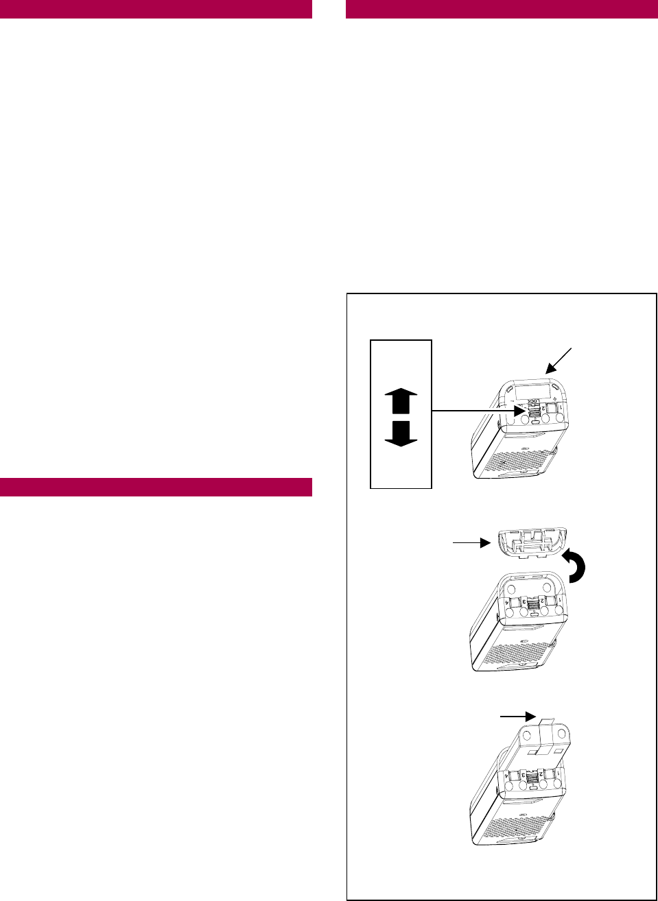
BATTERY REPLACEMENT
To replace the battery in the SST-144:
1. Hold the radio as shown in FIG-1(A)
2. Use your thumbnail to open the Door Latch, as
shown in FIG-1(A).
3. Lift and rotate the Battery Access Door to release
it as shown in FIG-1(B).
4. Use the Pull-tab to pull the Battery Pack out of
the case as shown in FIG-1(C).
5. Insert the replacement Battery Pack as shown in
FIG-1(C). Push the Battery in as far as possible.
6. Replace the Battery Access Door. Secure it by
closing the Door Latch as shown in FIG-1(A).
7. Be certain to firmly lock the Door Latch, as
shown in FIG-1(A).
BATTERY
ACCESS
DOOR
PULL-TAB
FIG-1: Batter
y
Replacement
(
A
)
(
B
)
(
C
)
LATCH
CLOSED
LATCH
OPEN
BATTERY
ACCESS
DOOR

BATTERY CARE SST-144
6
BATTERY MAINTENANCE
With daily use and recharging, a battery’s service life
is about one year. To ensure maximum service life,
follow these guidelines:
•DO NOT discharge a battery that is already “run
down.” If the battery cannot power your radio,
recharge the battery.
•DO NOT overcharge a battery. The standard
battery should not be left to charge continuously.
•Condition battery packs once a month as
directed in Battery Conditioning.
•Condition batteries that are run down.
•Charge batteries for 16 hours before storage,
and for 16 hours once a month thereafter.
•DO NOT charge batteries in temperatures colder
than about 45°F. Charging batteries in
temperatures above 95°C. does not harm them,
but can reduce charge capacity.
It is time to purchase a new battery:
•When the radio’s transmitter coverage decreases
or does not work at all.
•When the radio quits working after just a few
hours of use, even with a full overnight charge.
•When the battery is more than two years old.
The date of manufacture is stamped on every
battery. The first two digits indicate the year, the
last two digits the week.
BATTERY CONDITIONING
Due to the extended run time of the SST-144 radio,
some users may never fully discharge the battery
pack during normal use. Achieve maximum battery
life by fully discharging the battery periodically to
condition it.
After exposing the battery pack to many cycles of not
fully discharging it before recharging, the radio may
exhibit reduced battery capacity. This reduced
capacity is evident when, after several hours of use,
battery voltage drops while the radio is transmitting,
causing the radio to emit a dead battery warning tone
and shut itself off.
Condition battery packs by the following procedure as
either a preventive measure, or if you suspect
reduced capacity:
1. Use your radio throughout a normal working day
without charging.
2. Press and hold the On/ Volume Up and Volume
Down/ Off buttons simultaneously for 8 seconds
to place the radio in "open squelch" mode.
3. Release both buttons when you hear the radio
beep rapidly; it will then emit a loud "rushing"
noise. Press On/ Volume Up to maximize this
noise.
4. Put the radio away in a secure place (possibly a
desk drawer), where nothing can press against
the buttons to accidentally turn it off or cause it to
transmit. Allow the radio to run until it shuts off
when the battery is completely discharged. A
typical battery pack may require up to 8 hours to
completely discharge.
5. When the radio has shut off, charge it overnight
for 12-14 hours. The battery will be ready for use
with renewed capacity.
OPERATION SST-144
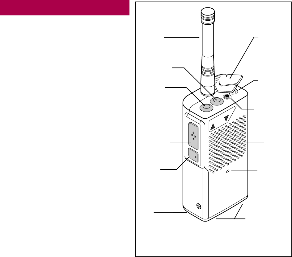
7
CH
ON OFF/HOLD
VOLUME
Antenna
Vol Down/Off
On/Vol Up
Audio
Accessory
Jack
Jack Cover
Charge Jack
Speaker
Microphone
Push-to-Talk
Channel
Selector
Battery Access
Door
(Case bottom) Battery Charger
Contacts
(Case bottom)
Fig. 2 Controls and Accessory Connectors
DESCRIPTION OF CONTROLS AND
CONNECTORS
Antenna
The flexible antenna radiates and receives radio
signals. Before using the radio, be sure the
antenna base is threaded fully into the radio’s
antenna bushing.
Use only the antenna(s) available from RITRON
for the SST-144. Do not attempt to substitute
with any other antenna.
On/Volume Up
This button switches on the radio, then increases
the volume if you continue to press.
Volume Down/Off
This button decreases the volume, then shuts off
the radio if you continue to press.
Push-To-Talk
The PTT activates the transmitter, and must be
held down while you talk into the microphone.
Release the PTT button to receive.
Channel Selector
Pressing this button selects the next channel.
When the maximum number of channels is
reached and you press this button, the radio
resets to channel 1.
Audio Accessory Jack
This jack connects speaker audio to optional
accessories, such as a remote speaker/
microphone or an earphone. For accessories
that have a two-plug connector, the smaller plug
is inserted into the charge jack.
This jack is also used to program the radio using
the optional PC programming kit.
Charge Jack
The battery may be charged through this jack
using a standard RITRON wall socket charger
cube. This jack also connects microphone audio
to the optional remote speaker/microphone.
Microphone
The microphone converts your voice into
electrical impulses, which are carried with your
broadcast to receiving radios. Hold the radio
about four inches away and talk into the
microphone while transmitting. Shouting does
not improve the listener’s reception.
Speaker
The speaker allows you to hear calls on your
channel.
Jack Cover
This rubber cover seals out dust and moisture, etc. Snap the
cover into the audio accessory and charge jack openings
when the jacks are not being used.
Battery Access (Case Bottom)
The battery door on the case bottom may be removed to
access the battery. (Refer to the Battery Replacement section
of this manual.)
Drop-in Charger Contacts (Case Bottom)
Two charger contacts in the bottom of the SST-144 radio case
allow the battery pack to be charged using an optional
RITRON drop-in charger (model BCC-PS.)

OPERATION SST-144
8
RADIO OPERATION
On-off/Volume
To switch on the radio - press the On/Volume Up
button. The radio will beep a number of times equal
to the current channel number.
To adjust the volume - press the volume up button
until you reach the desired level. You should hear
noise and any broadcasts on the channel.
To turn off the radio - press and hold the Off/Volume
Down button until two tones sound.
To determine whether the radio is on - press the
volume down button. If the radio is on, noise or
activity on the channel is heard.
Receive
To hear calls from other users - adjust the volume as
desired. The radio can receive broadcasts while the
Push-To-Talk button is not being pressed. Whether
or not you hear these broadcasts depends upon the
squelch settings.
There are two types of squelch used in the SST-144
portable. First is carrier squelch. This lets you hear
all broadcasts on your channel strong enough for the
radio to detect, and silences noise. Second is one of
the selective signaling or “tone squelch” formats
available on the SST-144. This allows you to screen
out “on-channel” broadcasts that do not carry the
correct code programmed for the radio.
Note: It is possible that the beginning of a call might
be missed while the radio is in battery saver
mode. If this happens, ask the caller to repeat
the message.
Selective Signaling Squelch
To activate tone squelch - simultaneously press both
of the volume buttons. Hold for a second or two
before releasing. When tone squelch is turned on,
the handheld sounds one beep. When carrier
squelch is on, the radio emits a "double beep."
Note: If you continue to hold down the volume
buttons after the beep (or double beep), the
radio will start beeping repeatedly. This
means that squelch is turned off. Release the
buttons. To restore squelch, press and hold
both of the volume buttons until the radio
sounds a beep or double beep.
Monitor
To monitor the channel - press one of the volume
control buttons. When you press the volume up or
the volume down button, squelch turns off and all
radio traffic on the channel (and noise) sounds in the
speaker.
Battery Saver
The handheld has a programmable "battery saver"
feature that conserves battery power. The battery
saver constantly checks the radio's transmitter,
receiver and controls for activity. If a number of
seconds pass without the receiver detecting a call,
and without the user operating a control, this feature
removes power from most of the radio.
During this "off-time," any activity restores full power.
Every few fractions of a second, the battery saver
applies power to the receiver, checking for
broadcasts. It is possible that the first part of an
incoming call might go unheard before activity is
detected and power restored. If this happens, the
caller can repeat his message. Once "radio contact"
is made, normal unhurried conversation can follow.
Transmit
Normally, you should not transmit until no one is
talking on the channel.
To transmit - hold down the Push-To-Talk button and
with the radio four inches away talk into the
microphone. Speak in a normal tone, since talking
louder will not improve the listener’s reception.
Channel Selection
To change channels - press and release the Channel
button. The radio will beep a number of times equal
to the current channel number. Pressing the Channel
button again will increment the channel and the radio
will beep the new channel number. For example, if
you select channel 2, the handheld will beep twice. If
the highest channel number is selected and you
press the Channel button, the radio will reset to
channel 1. A one-channel radio will beep only once
when you press the Channel button.

OPERATION SST-144
9
WHAT THE RADIO TONES MEAN
The handheld responds to certain instructions by
sounding a beep or series of tones. These tones can
tell you whether the radio is working as you expect.
Power On/Self Check “OK”
When it is first turned on, the radio runs a quick “self
test” to confirm basic functions. The radio then beeps
the number of times equal to the channel number
selected. The radio is then ready to use.
Error Tones
However, if the “self test” detects a diagnostic error,
an error tone sounds. Alternating tones (the second
is longer and lower pitched) indicate the radio
frequency synthesizer is malfunctioning. Turn off the
radio and try again. A long, low-pitched tone means
the battery voltage is too low to operate the radio. In
this case, recharge the battery. If you cannot correct
a problem, consult an authorized Ritron service
facility or Ritron.
Channel Select
When the Channel button is pressed, the radio beeps
a number of times equal to the current channel
number. Pressing the Channel button again will
increment the channel and the radio will beep the
new channel number.
Tone Squelch
When you press and hold both Volume buttons at the
same time, a single beep will sound to indicate that
tone squelch is on. A "double beep" means that
carrier squelch is on.
Recharge Battery Alert
As the battery voltage approaches the minimum
required “operating voltage” the radio will emit a short
beep every minute to alert the user that the battery
will soon need recharging. Once the battery charge
drops below the required "operating voltage," the
radio emits a long, low tone and turns itself off. If you
turn the radio back on, it will beep again and shut
itself off. Recharge the battery.
OPTIONAL RADIO TONES
The SST-144 can be programmed using the RITRON
PC Programmer for optional alert tones.
Receive Squelch Tone
A short tone sounds at the end of each received
transmission to indicate that you may transmit.
Busy Channel Transmit Inhibit
If a user is transmitting on your radio frequency
without your tone, you will not be allowed to transmit.
The radio will beep a series of long, low tones while
the PTT is held down (like a busy signal).
Transmitter Time Out
A low tone followed by a higher-pitched tone sounds
and the transmitter automatically shuts off if you hold
down the PTT button longer than the programmed
Time-out. The radio automatically switches to receive
mode. Authorized service personnel can turn off this
feature.
BELT CLIP INSTALLATION
If you are going to attach the belt clip to the handheld,
follow these instructions:
1. The belt clip is fastened to the radio case back
with the Philips head screw provided. Use the
screw included, since a longer screw might
damage the radio’s electronics.
Do not use petroleum solvents of any kind on the
radio. These can corrode the case.
2. Place the belt clip on top of the radio case back,
with the screw hole in the aligned with the hole in
the radio case.
3. Using the screw that came with this accessory,
attach the clip to the radio.

OPERATION SST-144
10
TROUBLESHOOTING
If you have trouble operating the handheld, review the
radio controls and operation sections. If you think the
radio is malfunctioning, check the following table.
GENERAL
The radio does not work at all.
• Make sure the battery is installed correctly, as
shown in FIG-1.
• Recharge or replace the battery. (See note 1.)
Operating features do not work exactly as expected.
• The radio has been factory or dealer
programmed for customized operation.
Reception is poor.
• Move to a different location. (Note 2.)
• Confirm that the proper antenna is connected to
the radio. (See p. 11, "Antenna.")
You cannot hear calls from other radios.
• Turn off tone squelch. (See Note 3.)
• Be certain your radio receives on the same as
the caller transmits. (Note 4.)
• Recharge the battery. (Note 1.)
Your calls cannot be heard in other radios.
• Make sure that your radio transmits on the
receive frequency of the radio(s) you want to call.
(Note 4.)
• Recharge the battery. (Note 1.)
TONE CODED SQUELCH
You cannot screen out calls from users outside of
your tone group.
• Make sure the channel is programmed with tone
squelch.
• Activate Tone (coded) squelch. (Note 7.)
You cannot hear Tone coded messages while in
Tone (coded) squelch.
• Confirm that the channel is programmed to
detect the same code as the calling radio(s)
transmits. (Note 7.)
Others in your tone group cannot hear your tone
coded messages.
• Verify that you transmit the same code as the
radio(s) you call are programmed to detect.
(Note 7.)
ERROR TONES
An error tone sounds when the radio is first
turned on.
• Replace the battery. (Note 1.)
• See "Error Tones" in the Operation section.
An error tone sounds while you are talking. (and
the transmitter shuts off).
• Refer to “Error Tones”
BATTERY
The battery loses its charge sooner than
expected.
• Review the battery charging instructions.
• Conserve the battery. (Note 5.)
• If the radio is used in extreme cold, warm the
radio under your coat. (Note 6.)
Notes
1. Try a battery pack from a working radio. If the radio in
question works with that pack, the original battery is
suspect. Charge the suspect battery as recommended
in this manual. Then, if the charged original battery
cannot power the handheld, try charging again with
another charger. If the battery still doesn’t hold a
charge, the pack should probably be replaced.
However, if the battery appears to be good after you try
the second charger, the first charger might be faulty. If
you think that an accessory is not operating properly,
contact your dealer or RITRON. (Radio accessories
come with a 90-day limited warranty.)
2. Reception can often be improved by moving a short
distance. This effect is more noticeable inside of
buildings. The range of these portables equipped with
a standard battery pack is about two miles (line-of-
sight).
3. If your radio does not detect calls from other radios on
the channel, turn off tone squelch. (Press both Volume
buttons at the same time - a double beep means that
tone squelch is off.)
4. If you want to hear a call, you must select a channel
that is programmed to receive the caller’s transmit
frequency. If you want to call another unit, you must
select a channel that is programmed to transmit the
other radio’s receive frequency. However, if you use a
repeater, your channel must be programmed to work
with the repeater’s transmit and receive frequencies.
(A radio channel can hold two separate operating
frequencies, one for Receive, the other for Transmit.)
5. Maximum power drain occurs while the radio transmits,
so don’t hold down the Push-To-Talk button more than
necessary. Battery power is used while the handheld is
left on to receive calls. If practical, switch off the unit.
6. In extreme cold, a battery’s charge capacity is greatly
reduced. If you use the radio in very cold weather,
periodically warm the portable underneath your coat if
possible. An optional remote speaker/microphone
would allow you to keep the radio under your coat while
transmitting and receiving.
7. In order for radios to communicate using Quiet Call,
they must be programmed with the same tone code.
Each code is unique, and your radio will respond only
to the code programmed. Press and hold both volume
buttons at the same time. A single beep means that
tone squelch is on. A double beep means that tone
squelch is off.
PROGRAMMING THE RADIO SST-144
11
PROGRAMMING METHODS
Each SST-144 can be programmed to operate on up
to 10 channels. The SST-144 may be programmed
using the Push-to-Talk switch or an optional RITRON
PC programming kit.
PTT (PUSH-TO-TALK) PROGRAMMING allows you
to program any channel to one of the radio
frequencies listed in Table 1 and any Quiet Call code
listed in Table 2. The radio will transmit and receive
on the programmed table frequency and QC code.
PC PROGRAMMING allows you to program any
frequency within the band and channel spacing of the
radio model. This method also lets you customize the
handheld with optional operating features.
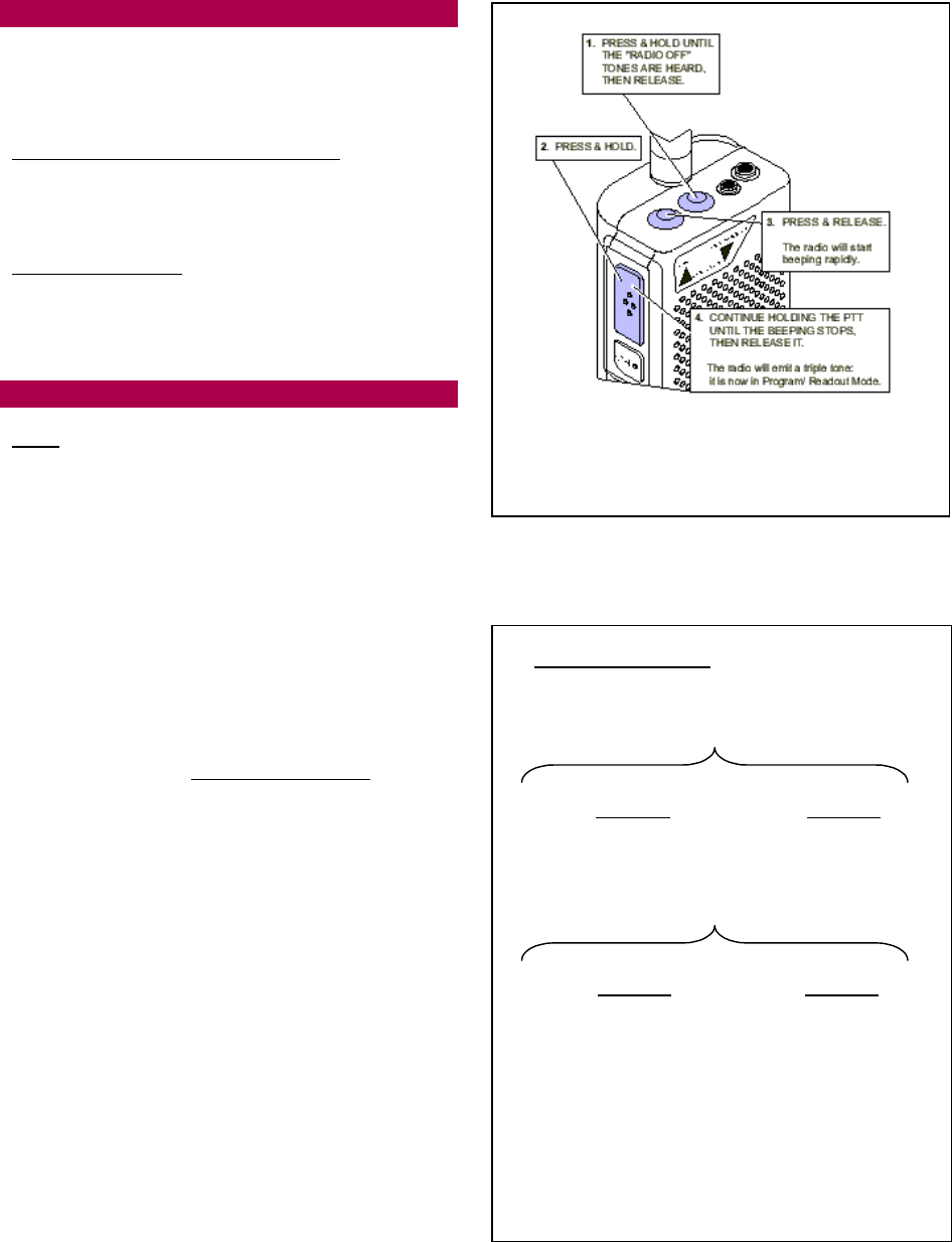
PTT (PUSH-TO-TALK) PROGRAMMING
Note: If the radio will not enter PTT program
mode, this feature has probably been turned off
using the optional PC programming kit.
Reading Out a Radio Channel’s Contents
1. Place the radio in Program / Readout mode as
described in Fig-3.
2. Press the Channel Selector button to select the
radio channel you would like to read out.
3. Press and release the Volume Up button.
4. The radio will emit a series of beeps, pause, and
then begin another series. Four series of beeps
will be heard, with each series representing a
digit. The number of beeps in a series is equal
to the digit. (See CHANNEL READOUT)
5. Write down each digit while the radio pauses.
List the digits in the order that you hear them.
6. The first two digits represent the frequency as
shown in Frequency Table 1 on page 13.
7. The second two digits represent the QC
(CTCSS) tone frequency as shown in Quiet-Call
Tone Code Table 2 on page 13.
8. To read out another channel, follow steps 2
through 7.
9. Turn the radio off to exit Channel Readout mode.
Notes:
1. Ten (10) beeps = the digit zero (0)
2. The radio will beep out “44” as a tone code if it
has been programmed for “No Tone”.
3. A radio that has been PC-programmed with any
frequency not listed in Frequency Table 1, page
13, will emit the error tone on content readout.
Fig. 3 PLACING THE RADIO IN PTT
PROGRAM / READOUT MODE
CHANNEL READOUT:
FREQUENCY CODE
# of beeps
in series
1st
digit
∗
2nd
digit
∗
# of beeps
in series
TONE CODE
# of beeps
in series
3rd
digit
∗
4th
digit
♦
# of beeps
in series
Notes:
∗Pause after entering each digit. The radio
will emit a low tone, separating one digit
from the next.
♦ The radio sounds a triple beep when PTT
channel programming is complete.

PROGRAMMING THE RADIO SST-144
12
PTT Programming a Radio Channel
Four valid digits must be entered for the radio to
accept PTT programming. The first two digits entered
are the frequency code from Table 1, followed by the
two digits for the QC code from Table 2.
1. Place the radio in Program / Readout mode as
described in Fig-3 on page 11.
2. Press the Channel Selector button to select the
radio channel you would like to program.
3. Enter the first digit by pressing the PTT button
the number of times equal to the digit’s value.
4. Pause after the digit is entered, a low tone will
sound indicating that the digit has been
accepted.
5. Enter the second, third and fourth digits using the
same method as the first digit.
6. Press the Volume Up button to enter the new
channel programming. The radio will emit a triple
beep confirmation tone to indicate that
programming has been accepted.
7. To program another channel, follow steps 2
through 6.
8. Turn the radio off and then on again – the radio
is now ready for use.
Notes:
1. To enter the digit zero ( 0 ), press the PTT ten
times.
2. Program “44” to enter “No Code” for Quiet Call.
You must enter “44” to match radios not having
tone codes.
3. An error tone will sound if you attempt to save an
incorrect digit. Turn the radio off, check the
digits you are attempting to enter, then start over
again.
4. If you make a PTT click error, turn the radio off
then on, and start over.
5. If the radio does not emit a confirming triple tone
when you attempt to enter Program / Readout
mode, the radio was dealer customized to
disable PTT programming.
6. Refer to the Frequency Table 1 and Tone Code
(Quiet Call) Table 2 on page 13.
Return to Normal Operation
After you finish programming, turn the radio off and
then on again. The radio will beep when it is ready for
normal operation.
PTT Programming Mistakes
Invalid Entries An error tone means that
you tried to save an invalid entry. No programming
changes are made in this case. A triple tone will
sound next indicating that the radio is still in
programming mode, and ready for an entry.
PTT Entry Mistakes If you press the PTT five
times when you intended four, for example, or if you
just lose count, do not press the Volume Up button to
store the entry. Instead, start over by turning the
radio off and placing the radio in programming mode
again.
PTT CHANNEL PROGRAMMING:
FREQUENCY CODE
# of beeps
in series
1st
digit
∗
2nd
digit
∗
# of beeps
in series
TONE CODE
# of beeps
in series
3rd
digit
∗
4th
digit
♦
# of beeps
in series
Notes:
∗Pause after entering each digit. The radio
will emit a low tone, separating one digit from
the next.
♦ The radio sounds a triple beep when PTT
channel programming is complete.

PROGRAMMING THE RADIO SST-144
13
Code Frequency Description
01 154.600 Green Dot
02 154.570 Blue Dot
03 151.625 Red Dot
04 151.955 Purple Dot
05 151.925
06 154.540
07 154.515
08 154.655
09 151.685
10 151.715
11 151.775
12 151.805
Table 1 – PTT Programming Frequency Table
QC Freq QC Freq
Code (Hz) Code (Hz)
01 67.0 27 167.9
02 71.9 28 173.8
03 74.4 29 179.9
04 77.0 30 186.2
05 79.7 31 192.8
06 82.5 32 203.5
07 85.4 33 210.7
08 88.5 34 218.1
09 91.5 35 225.7
10 94.8 36 233.6
11 97.4 37 241.8
12 100.0 38 250.3
13 103.5 39 69.4
14 107.2 40 159.8
15 110.9 41 165.5
16 114.8 42 171.3
17 118.8 43 177.3
18 123.0 44 No Tone
19 127.3 45 183.5
20 131.8 46 189.9
21 136.5 47 196.6
22 141.3 48 199.5
23 146.2 49 206.5
24 151.4 50 229.1
25 156.7 51 254.1
26 162.2
Table 2 – Quiet Call Codes and Frequencies
COMPUTER SOFTWARE COPYRIGHTS
The RITRON, Inc. products described in this manual
include copyrighted RITRON, inc. computer
programs. Laws in the United States and other
countries grant to RITRON, inc. certain exclusive
rights in its copyrighted computer programs, including
the exclusive right to distribute copies of the
programs, make reproductions of the programs, and
prepare derivative works based on the programs.
Accordingly, any computer programs contained in
RITRON, inc. products may not be copied or
reproduced in any manner without the express written
permission of RITRON.
The purchase of RITRON, inc. products does not
grant any license or rights under the copyrights or
other intellectual property of RITRON, inc., except for
the non-exclusive, royalty fee license to use that
arises in the sale of a product, or as addressed in a
written agreement between RITRON, inc. and the
purchaser of RITRON, inc. products.
PC COMPUTER PROGRAMMING
RITRON’s programming kit allows programming of
the SST-144 model radios using a PC compatible
computer. An adapter cable connects the radio to a
computer’s serial communications port. Once the
cable is hooked up, the user inserts the diskette
provided into his computer’s floppy disk drive and
loads a software program.
This program transfers data between radio and
computer memory, and includes on-screen
instructions and help. Radio data may be saved to
the computer’s hard disk in order to program other
radios.
The PC Programming Kit Includes:
1) Ritron Transceiver programming software, which
is contained on 3.5" diskettes.
2) Installation instructions and a registration form.
3) Ritron PC to radio adapter cable, which is
terminated at one end with a DB-25F connector,
at the other end with a modular plug. The DB-25
plugs into the computer’s serial port, the modular
plug into the SST-SRVBD modular jack.
4) An adapter for use with SST-144 portables. This
adapter mates the modular plug to a 3.5 mm
plug, for connection to the handheld audio jack.
The PC Programming Kit Requires:
A PC compatible computer with Windows 95 or later.
The computer must have an RS-232 serial port and a
minimum of 2MB available on the hard disk drive for
installation.

PROGRAMMING THE RADIO SST-144
14
Programmable Features
The following features may be programmed on a per
channel basis, or will affect all channels together.
Feature RangeFactory Setting
Automatic Inactivity Y - N Y -
Turn-off
Battery Saver Enable Y - N Y -
Battery Saver Off Time 0 – 8 1 -
(seconds)
Beep Volume Level F-C C -
(Fixed or Controlled)
Beep Fixed Level 0 – 100% 50% -
(percent of full volume)
Busy Channel TX Inhibit Y - N N √
Carrier Only, No Codes - - √
Channel Beep Rate S – F S -
(Slow or Fast)
Channel Selection Mode I – E I -
(Increment or Enter)
Digital Tone Invert RX Y - N N √
Digital Tone Invert TX Y - N N √
Digital Quiet Call (DCS) - - √
Disable Monitor Y - N N √
Number of Channels 0 – 10 4 -
Narrow Band Channel Y - N N √
PTT Programming Y – N Y -
Enabled
Quiet Call (CTCSS) See Table 2 - √
Receive Squelch Tone Y - N N √
Squelch Tightener 0 - 7 0 √
Transmit Power L - H H √
(Low or High)
TX Time-out Enabled Y – N Y -
TX Time-out Timer 0 – 255 60 -
(seconds)
Turn On To Medium Y - N Y -
Volume Level
Descriptions of Features
Automatic Inactivity Turn-off - The radio automatically
shuts itself off if four hours go by without the micro-
controller detecting input from the volume, PTT or
channel controls.
Battery Saver - Enabling this option allows the radio
to go into battery saver mode when the radio remains
idle. The power saver begins after eight seconds of
inactivity.
Battery Saver Off Time - This is the cycle time that
the radio is off in battery saver mode before it checks
for a received signal. A long Battery Saver Off Time
may cause the user to miss the beginning of the first
message when in battery saver mode.
Beep Volume Level - The radio can be programmed
for a fixed beep volume or for a beep volume that is
adjusted with the Volume controls. If fixed beep
volume is selected, the fixed level can be set between
0 – 100%.
Busy Channel Transmit Inhibit - This keeps the radio
from broadcasting if the channel is busy, and is often
used in conjunction with Disable Monitor. If you press
the PTT when the channel is busy with a signal not
intended for your radio (not carrying your tone code),
this feature sounds a "busy" tone in the speaker and
keeps the transmitter turned off.
Channel Beep Rate - The rate at which the channel
indicator beeps occur can be set to fast or slow.
Channel Selection Mode - This feature allows the
channel selector to increment or enter the channel.
The channel number is "beeped out" when the
channel button is first pressed. The channel is not
changed. In increment mode the radio is changed to
the next available channel if the channel button is
pressed again within three seconds. In enter mode
the user must press the channel button the number of
times equal to the channel they wish to select.
Digital Quiet Call RX Invert - The programmed code
is inverted for receive mode only.
Digital Quiet Call TX Invert - The code is inverted for
transmit mode.
Disable Monitor - This function may be programmed
to keep the radio user from listening to other
licensees on a shared channel. QC or DQC must be
used for this option to have any affect, and the
Encode Only feature disabled.
Maximum Number of Channels - The number of
channels available on the radio can be set from 1 to
10.
Narrow Band Channel - Any channel can be set to
operate in narrow band mode, reducing the transmit
deviation to 2.5 KHz.
PTT Programming Mode Enabled - This feature
allows channel programming from a table of pre-
determined frequencies using the radio PTT switch.

PROGRAMMING THE RADIO SST-144
15
Quiet Call (CTCSS)- Programming a Quiet Call code
allows you to screen out transmissions that do not
carry your code. Your code is broadcast when you
press the PTT to make a call.
Quiet Call Encode Only - The Quiet Call code
programmed for the channel is transmitted with your
calls. However, no Quiet Call code is programmed
for receive mode, allowing all traffic on the channel to
be heard.
Receive Frequency - The radio frequency that
receives broadcasts from other units.
Receive Squelch Tone - The receiving radio beeps at
the end of each received transmission.
Squelch Tightener - This feature reduces distant "co-
channel" or other interference for channels that are
not programmed with Quiet Call. Carrier squelch is
set for maximum sensitivity at the factory, but may be
adjusted to mute weak signals
Transmit Frequency - The radio frequency that
broadcasts to other units.
Transmit Power – Any channel can be set to transmit
at high or low power.
Transmit Time Out Timer - This feature automatically
shuts off the transmitter (ending your call) if you hold
down the PTT button continuously for 60 seconds.
The radio sounds a tone when the transmitter shuts
off.
Turn On To Medium Volume Level - The volume level
is at mid-range when the radio is first turned on.
Normally, the volume level is low when the radio is
turned on.

THEORY OF OPERATION SST-144
16
INTRODUCTION
The SST-144 is a four-channel handheld transceiver
built on a single multi-layer printed circuit board. Both
sides of the main printed circuit board are populated
with components, with the bottom side containing
only surface mounted components.
The SST-144 is frequency synthesized, with all
functions of the radio controlled by microcontroller.
POWER SUPPLY AND VOLTAGE DISTRIBUTION
The SST-144 is powered by an internal 6-cell
rechargeable battery pack. The battery pack supplies
power to the radio via two contact terminals that are
connected to the PCB through P302. F301 is a 3A
fuse in series with P302 for short circuit protection.
The battery pack may be charged through 2.5 mm
charge jack J301 via CR302 and F301. Zener diode
CR301 prevents the batteries from discharging
through the charger accessory, stops a reverse
voltage from being applied to the battery pack
through J301, and prevents a high voltage from being
applied to the radio circuitry.
SW301 ON/VOL UP switch is pressed to turn on the
SST-144, turning on voltage pass transistor Q304 via
R302 and CR303. Q304 supplies power to IC309, a
+5 VDC regulator used to power microcontroller
IC301. Pin 13 of IC301 turns on Q303, which keeps
Q304 turned on after SW301 has been released.
Power is removed from the SST-144 by pressing the
VOL DN/OFF switch SW302 until a beep is heard
from the speaker, at which time Q304 is turned off.
+5 VDC regulator IC309 supplies power directly to
microcontroller IC301, bilateral audio gates IC304,
reference oscillator Y302, synthesizer IC401, and
PTT detect transistor Q302.
The T/R output at Pin 11 of IC301 lets Q101 switch
the regulated +5 VDC to the receiver. Pin 11 of
IC301 will also turn on Q202, which turns on voltage
pass transistor Q201. With Q201 emitter connected
to the +VBATT battery supply, the collector output is
connected to the emitter of Q202 through voltage
divider R202/R203, whose values are selected to limit
the TX+V voltage to +6 VDC.
Power Strobe
The SST-144 handheld includes a power strobe
feature, which reduces battery current drain by
periodically removing voltage from part of the radio.
The strobe off cycle time is programmable using the
PC Programming Kit. The +5V SW power strobe
output at Pin 10 of IC301 controls Q306, which
switches the regulated +5 VDC to the audio
processing circuitry and the synthesizer circuitry.
This includes IC303A 2.5 VDC (Vag) for bias on
audio processing circuitry, IC303C audio high pass
filter, IC308 and IC305A audio low pass filter for sub-
audible frequencies, IC305B audio limiting amplifier,
IC306 digital potentiometers, IC303B audio summing
node amplifier, and IC303D audio low pass filter.
Low Battery Voltage Detection
Battery voltage is measured at A/D input Pin 16 of
IC301 through voltage divider R303/R305. The radio
will emit a periodic beep if low battery voltage is
detected, and will turn the radio off if the battery
voltage drops below +5 VDC. This is to protect the
microcontroller and its EE memory from corruption
due to low supply voltage.
REFERENCE OSCILLATOR
Reference oscillator Y302 is a 1.5 ppm temperature
controlled, voltage controlled oscillator (TCVCXO)
operating at 14.4 MHz. The Pin 4 output of the
TCVCXO provides a reference for the frequency
synthesizer IC401 at Pin 20. IC401 is programmed to
provide an output at Pin 1 that is ¼ of the reference
(3.6 MHz), which is applied as a reference oscillator
to Pin 27 of IC301 microcontroller. The Y302 pin 4
output is also multiplied up to 43.2 MHz by Q105 and
its associated circuitry to provide a receiver 2nd local
oscillator signal.
SYNTHESIZER
The SST-144 radio is built around a common phase-
locked loop (PLL) that consists of a voltage-controlled
oscillator (VCO) and a frequency synthesizer. The
PLL generates both the receiver 1st local oscillator
and transmitter carrier signals. Control signals from
microcontroller IC301 and Reference oscillator Y302
are routed to frequency synthesizer IC401 per the
following chart:
Pin Numbers
IC301 Y302 IC401
Clock 12 - 18
Data 5 - 19
Latch 20 - 17
LD 12 - 2
T/R SW 11 - -
REF IN - 4 20
REF OUT 27 - 1
+5 SW 10 - 12
+5V 1, 15, 28 2 5, 14
Q404, CR401, C414 and associated components
provide a filtered supply for the VCO oscillator and
buffer amplifiers.
Prescaler Divider / Synthesizer Controller
IC401 contains both a prescaler and synthesizer
controller. The prescaler squares and divides the
VCO output present at pin 11 by either 64 or 65,
determined by a synthesizer controller logic signal.
The exact number of times the prescaler is instructed

THEORY OF OPERATION SST-144
17
to change divisors is determined by the channel
frequency.
IC401 contains a digital phase detector that works as
follows: when an operating channel is changed or the
receive/transmit mode switched, a new synthesizer
operating frequency is selected. Microcontroller
IC301 clocks new data into IC401 internal buffer in
synchronization with clock pulses. The channel
information is stored in EE memory of IC302 and is
loaded into RAM when the channel is selected.
Once new data is loaded into the buffer, a single
pulse from IC301 appears at IC401 to instruct the
synthesizer controller to latch and execute the new
data. IC401 utilizes internal circuitry to determine
whether the present VCO output frequency is correct
by comparing the phase and frequency of the VCO
signal at Pin 11 to the 14.4 MHz reference oscillator
at Pin 20. IC401 produces an output signal at Pin 6,
a single-ended phase/frequency detector output,
proportional to the phase difference between the two
input signals.
The loop filter C429, C427, R419, R420, R418, and
C426 transform the Pin 6 output signal to a DC
voltage for application to the VCO tuning varactor
CR402. The synthesizer system is “locked” when the
phase and frequency of both the reference and the
divided VCO signal are the same.
The maximum amount of current this output can sink
or source is determined by the value of R421 tied to
Pin 8 of IC401, with the output current programmable
to 25, 50 or 100% of maximum.
VCO / Buffer Amplifiers
Q403, L401, L406, CR402 and associated
components form the VCO (Voltage Controlled
Oscillator), a resonant circuit that oscillates at
frequencies from 150 MHz in transmit to 205 MHz in
receive (receive frequency + 43.65 MHz) to. Varying
the voltage at CR402 changes the varactor
capacitance, which in turn alters the VCO output
frequency.
When in receive mode a +5 VDC T/RSW signal is
applied to Q406, which turns on Q405 to draw current
through pin diode CR404 and L403. With CR404
biased on, L402 is effectively shorted to ground,
shifting the VCO frequency up 43.65 MHz.
Q401 and Q402 are buffer amplifiers, with Q401
feeding in the input of the synthesizer at Pin 11, the
receiver 1st local oscillator and the transmitter pre-
amplifier.
Oscillator Modulation
When the SST-144 is in transmit, modulation balance
control IC306E passes TX audio through to the VCO
modulation input at R416. TX audio is applied to
varactor CR403 to modulate the VCO. TX audio is
also routed to the Pin 1 input of TCVCXO reference
oscillator Y302. Low frequency tones modulate the
reference oscillator because the synthesizer is not
able to track them.
DIGITAL POTENTIOMETERS
IC306 contains 6 digital potentiometers programmed
by IC301, sharing the same clock and data outputs
used by the synthesizer and a separate Digital Pot
Latch signal from Pin 8. The digital potentiometers
are used in conjunction with IC303B, a summing
node amplifier used for modulating the VCO and
reference oscillator. IC306A, B, D, E, and F can only
be changed through serial programming, and can
only be performed by an authorized licensed RF
technician.
IC306A is connected through R352 to the Pin 6 input
of IC303B. IC306A adjusts the DC output of IC303B
to tune the reference oscillator frequency.
IC306B is connected to the Pin 2 Gate control of RF
power transistor Q203 to adjust transmitter power
output.
Volume control IC306C applies the processed voice
band signals at IC303D to audio amplifier IC307
when in receive mode. Depressing the ON/VOL UP
switch SW301 increases the setting of IC306C while
VOL DN/OFF switch SW302 decreases it.
Transmitter tone deviation control IC306D applies the
output of the selective signaling low-pass filter IC308
to the Pin 6 input of IC303B through R350. IC306D is
completely closed in receive mode.
Transmitter modulation balance control IC306E is
used to apply the Pin 7 output of IC303B to the VCO
modulation input. This will set the ratio of the
modulating signal applied to the VCO and the
reference oscillator. IC306E is completely closed in
receive mode.
Transmitter voice deviation control IC306F applies
the processed voice band signals at IC303D to the
Pin 6 input of IC303B through R349. IC306F is
completely closed in receive mode.
RECEIVER
As mentioned before, Q101 switches the regulated
+5 VDC to the receiver. The +VRX receiver voltage
is switched at the strobe duty cycle if programmed for
power strobe.
RF Amplifier
A received signal from the antenna passes through a
low-pass filter (L207, C218, C217, L208, C219, and
C222) to the receiver headend. L101, L103, and the
associated capacitors form a bandpass filter ahead of
low-noise RF amplifier Q102. The amplified RF
signal is applied to a 2-pole bandpass filter consisting
of L104, L105, and associated capacitors.
THEORY OF OPERATION SST-144
18
1st Mixer
The amplified received input signal is applied to the
gate of FET mixer Q103. The 1st local oscillator
signal from the synthesizer module is applied to the
source of Q103. L106, C117 and C118 tune the drain
output of Q103 to 43.65 MHz and apply it to YF101, a
43.65 MHz two-pole crystal filter. Q104 and
associated components amplify the 43.65 MHz IF
signal and apply it to the input of the 2nd mixer at Pin
16 of IC101.
FM Receiver Subsystem
A multi-function integrated circuit, IC101 and
associated components for the FM-receiver
subsystem. The subsystem performs the following
functions: 1) 2nd mixer, 2) 2nd IF amplifier, 3) FM
detector, and 4) noise amplifier.
The Pin 4 output of 14.4 MHz reference oscillator
Y302 is multiplied up to 43.2 MHz by Q105 and
associated components. This signal is applied to the
2nd local oscillator input at Pin 1 of IC101. The 43.65
MHz signal at Pin 16 and the 2nd local oscillator are
mixed, with the resulting 450 KHz output signal
appearing at Pin 3. This signal is filtered by a 450
KHz 6-pole ceramic filter YF102 and applied to the
input of the limiting IF amplifier at Pin 5. IC101 Pin 6
is the de-coupled input to the IF amplifier, Pin 7 the
limited IF output signal. An internal quadrature
detector, whose center frequency is determined by
450 KHz quadrature coil T101, detects the FM IF
signal. One input of the quadrature detector is
connected internally to the IF signal at Pin 7, while
the other input is the phase-shifted signal from T101
at Pin 8.
Demodulated audio appears at Pin 9, where a low-
pass filter (R114, C130) removes spurious quadrature
output prior to application to the voice/tone
conditioning audio circuitry. Demodulated audio from
Pin 9 is applied to the Pin 10 input of a noise
filter/amplifier consisting of R112, C123, C124, R110,
R111 and R113. The Pin 11 output of the noise
amplifier is applied to a biased noise detector CR103,
with the output connected to an A/D input of IC301 at
Pin 19. The SST-144 is serial programmed to set the
squelch threshold and hysteresis.
Voice / Tone Conditioning in Receive Mode
SST-144 audio conditioning filter circuits are shared
with the transmitter. The same high-pass
filter/amplifier (IC303C and associated components)
used in receive voice band conditioning is used in the
transmit band. Similarly, the low-pass filter (IC308
and associated components) used for selective signal
tone decode filtering is also used for selective signal
encoding. Altering circuit configuration with bilateral
switches IC304A, B and C permits the use of the
same audio filtering system for both transmit and
receive modes.
After R114 and C130 remove the 450 KHz element
from the demodulated audio output at Pin 9 of IC101,
C333 couples the audio signal to bilateral switch
IC304C for subaudible tone detection and connection
to IC304A for voice band audio processing.
Voice Band
Bilateral switch IC304A passes the received audio
signal to the input of IC303C, which along with its
associated components for a high-pass filter/amplifier
circuit that attenuates audio signals below 300 Hz.
The output of IC303C is applied to the input of
IC305B limiting amplifier. Bilateral switch IC304B is
switched in receive to insert C351 into the feedback
circuit of IC305B, providing de-emphasis of the
received audio signal. Bilateral switch IC304B also
removes R335 from the Pin 6 input to reduce the gain
and prevent limiting.
The output from IC305B is applied to the input of
IC303D, which along with its associated components
form an 18dB/octave low-pass filter for frequencies
above 3000 Hz.
The output of IC303D is connected to IC306C volume
control prior to connection to audio amplifier IC307.
The output of IC303D is also connected to IC306F
voice deviation control, which is completely closed in
receive mode to prevent received signals from
modulating the VCO and reference oscillators.
Audio frequency tones from Pin 24 of microcontroller
IC301 are applied to the Pin 6 input of IC305B to
provide the SST-144 alert tones.
Sub-Audible
Bilateral switch IC304C passes the received audio
signal to the input of IC305A, which amplifies the
signal and applies it to the Pin 2 input of IC308, a 5-
pole low-pass filter that attenuates frequencies above
250 Hz.
The output at Pin 5 is applied to an A/D input of
IC301 at Pin 18 for tone decoding. An internal digital
signal processing routine programmed into
microcontroller IC301 is used to decode the correct
selective signaling code. The output at Pin 5 of
IC308 is also connected to tone deviation control
IC306D, which is completely closed in receive mode
to prevent received subaudible tone signals from
modulating the VCO and reference oscillators.
Audio Amplifier
Receive audio from volume control IC306C is applied
to the Pin 2 input IC307, a 1 Watt audio amplifier.
C365 couples the Pin 5 output to the internal 8Ω
speaker SP301 via audio jack J303.
Microcontroller IC301 Pin 22 switches DC power to
the audio amplifier by turning on Q307, which then
turns on pass transistor Q308 to apply battery voltage
to Pin 6 of the audio amp. CR307 prevents an
inadvertent DC voltage at J303 from damaging the
audio amplifier.

THEORY OF OPERATION SST-144
19
ANTENNA SWITCHING / LOW PASS FILTER
A low-pass filter comprised of filter L208, C222,
C219, C218, C217, L207, and C220 removes
harmonics from the transmitter output before applying
the RF signal to the antenna. Received signals pass
through the low-pass filter before entering the
receiver RF amplifier circuitry.
Two PIN diodes (CR201, CR101) and associated
components form the antenna switching circuit. With
the SST-144 in receive mode, no voltage is applied to
the PIN diodes and they do not conduct. This reverse
biases CR201 to prevent the transmitter amplifier
from affecting the receiver tuning and removes
CR101 from the receiver input. Incoming signals
from the antenna pass through the low-pass filter,
then L206 and C101 to the receiver headend.
When the SST-144 is switched into transmit mode,
transmitter supply voltage is switched on by Q201
and Q202 and applied to R207. Current flows
through R207, L205, CR201, L206 and then CR101
to ground, forward biasing the PIN diodes. CR201
passes transmitter RF power to the antenna while
CR101 shunts the receiver RF amplifier input to
ground. L206 provides sufficient impedance to
isolate the transmitter power from the receiver RF
amplifier.
TRANSMITTER
Keying
The SST-144 transmitter is keyed when PTT switch
SW304 is depressed. Electret condenser
microphone M301 is connected in series to ground
with the PTT switch, which when depressed draws
current through M301, SW304, CR304 and R307 to
turn on pass transistor Q302. Q302 then turns on
Q301 to pull the TX Key Pin 2 input of microcontroller
IC301 low. The microcontroller T/R output at Pin 11
then goes high to turn on Q202, which turns on pass
transistor Q201 to apply +6VDC to the transmitter as
described previously. The transmitter can also be
keyed through J301 with an audio accessory that
inserts a microphone and PTT switch in series to
ground, drawing current through CR304.
+VTX Supply
With the transmitter enabled as described above, the
+VTX voltage from Q201 is applied to transmitter RF
amplifier Q204. +VTX supply also forward biases the
PIN switching diodes CR201 and CR101 as
previously described. The transmitter RF final
amplifier Q203 is powered by the battery supply.
The Pin 11 T/R output of microcontroller IC301 can
be PC programmed to hold the transmitter on after
the PTT switch has been released to allow tone
related turn-off codes for squelch tail elimination.
Power Amplifier
Q204 and associated components amplify the VCO
signal and apply it to the input of RF Final amplifier
module Q203 at Pin 1. The 50Ω output of Q203 is
matched to the antenna switching circuitry and
applied to the antenna through the low-pass filter.
The RF power output is programmable by a licensed
RF technician. The SST-144 can be programmed on
a channel-by-channel basis for low or high power
operation. The power control digital Potentiometer
IC306B is used to adjust the Q203 gate voltage and
set RF power output.
Voice / Tone Conditioning in Transmit Mode
SST-144 audio conditioning filter circuits are shared
with the receiver. The same high-pass filter/amplifier
(IC303C and associated components) used in receive
voice band conditioning is used in the transmitter
voice band. Similarly, the low-pass filter (IC308 and
associated components) used for sub-audible tone
decode filtering is also used for tone encode. Altering
circuit configuration with bilateral switches IC304A, B
and C permits the use of the same audio filtering
system for both transmit and receive modes.
Voice Band
M301 microphone audio is passes through CR304,
C334 and is switched by IC304A to the input of
IC303C, which along with its associated components
form a high-pass filter/amplifier circuit that attenuates
audio signals below 300 Hz. The output of IC303C is
applied to the input of IC305B limiting amplifier.
Bilateral switch IC304B switches R335 in parallel with
R336, raising the gain of limiting amplifier IC305B for
full limiting of the transmitter voice audio. The output
of IC305B is applied to the input of IC303D, which
along with its associated components form an 18
dB/octave low-pass filter for frequencies above 3
KHz. The output of IC303D is applied to voice
deviation control IC306F, which sets the level of the
processed transmitter audio applied to summing node
amplifier IC303B used to modulate the VCO and
reference oscillator.
Sub-Audible
Microcontroller IC301 generates the sub-audible
selective signaling encode waveforms at Pin 21 and
applies them to the input of buffer amplifier IC305A.
The output of IC305A is applied to the input of IC308,
a 5-pole low-pass filter that attenuates frequencies
above 250 Hz. C342 and C343 set the corner
frequency of the low-pass filter, with C342 switched in
by Pin 7 of IC301 to lower the corner frequency for
lower tones. The output of IC308 is applied to tone
deviation control IC306D, which sets the level of the
transmitter sub-audible encode tones applied to
summing node amplifier IC303B used to modulate
the VCO and reference oscillator.

THEORY OF OPERATION SST-144
20
MICROCONTROLLER
The SST-144 handheld transceiver is electronically
controlled by IC301, an 8-bit microcontroller. IC301
has four 8-bit A/D inputs for processing analog
signals.
PIN DESCRIPTION
1 RESET is connected to the SST-144 +5V to start
the radio in a known state on power up.
2 TX KEY input is pulled LOW when either the
internal or external PTT switch is pressed to
initiate transmitter operation.
3 AUDIO GATE ENABLE controls analog switches
IC304A and B to configure the shared audio
processing circuitry for receive operation when
LOW, and for transmitter operation when HIGH.
4 SERIAL DATA INPUT links the microcontroller to
communications from an external data terminal
via J303 RING connection. This allows
programming of the SST-144 EEPROM memory
used to store channel frequency and
configuration information.
5 DATA output sends serial data to frequency
synthesizer IC401 to program frequency
information, IC302 EEPROM memory, and to
IC306 to set the digital potentiometers.
6 EECLOCK output sends serial data clock pulses
to EEPROM IC302 when reading or writing.
7 LOW-PASS CUT-OFF output goes LOW to lower
the cut-off frequency of IC308 when the radio is
on a channel programmed for a CTCSS tone
below 150 Hz. This output is in a tri-state OPEN
condition for all other tones.
8 DIGITAL POT LATCH sends a single positive
pulse after data has been sent to IC306 to latch
the new data and change the digital
potentiometers to the new programmed settings.
9 LED output goes LOW when the radio is on
channel 1 and is HIGH for all other channels.
10 +5V SW output goes HIGH at a programmable
periodic rate to remove the +5VSW supply from
various circuits in the radio, thus conserving
battery life. In normal transmit or receive mode
this output is LOW.
11 T/R SWITCH output is connected to the
Synthesizer circuitry to shift the frequency of the
VCO oscillator used in both transmit and receive.
The output is HIGH in transmit and LOW in
receive. T/R output is also used to switch supply
voltage to the transmit and receive circuits.
12 CLOCK output sends serial data clock pulses to
frequency synthesizer IC401 and digital
potentiometers IC306 when programming these
devices.
13 +V SW output is HIGH when the radio is turned
on, keeping pass transistor Q304 turned on via
Q303 to supply power to the radio.
14 GROUND
15 VREFH sets the upper reference level for the A/D
and is connected to the regulated +5 VDC.
16 A/D input BATTERY is used to measure the
battery voltage for low and dead battery
detection. This input also serves as the ON/VOL
UP input, and is pulled LOW when SW301 is
depressed to turn on the radio and raise the
receiver speaker audio level.
17 A/D input VOL DN/OFF is pulled LOW when
SW302 is depressed to lower the receiver
speaker audio level and turn off the radio. This
input also serves as CHANNEL input, and goes
to 2.5 VDC when channel selector switch SW303
is pressed to change the radio to the next
programmed channel.
18 A/D input TONE DECODE accepts the received
QC (CTCSS) and DQC (DCS) waveforms after
signal processing for decode analysis.
19 A/D input RSSI is used to measure the output
voltage of the noise filter for squelch detection.
20 LATCH output goes LOW to allow serial data to
frequency synthesizer IC401 and goes HIGH to
latch the data, allowing the synthesizer to
execute the new frequency information.
21 TONE ENCODE outputs generate the QC
(CTCSS) and DQC (DCS) encode waveforms for
signal processing prior to modulating the VCO in
transmit mode.
22 AUDIO AMP ENABLE output goes HIGH to apply
power to audio amp IC307 for receiver speaker
audio or radio alert tones.
23 RX AUDIO GATE ENABLE switches IC304C for
receive operation when LOW, and for transmitter
operation when HIGH.
24 BEEP output generate the radio alert tones
heard in the speaker.
25 See Pin 4
27 REFERENCE OSCILLATOR INPUT has the 3.6
MHz reference signal from the synthesizer.
28 +5 VDC VDD supply voltage.

ALIGNMENT PROCEDURE SST-144
21
WARNING!
An authorized RF service technician must perform
test and alignment of the SST-144. Do not attempt
service of the SST-144 if not completely familiar
with the operation of frequency synthesized radio
operation. The SST-144 can operate in both
Narrow Band (2.5 KHz deviation) and Wide Band
(5 KHz deviation) systems.
RECOMMENDED TEST EQUIPMENT
1) 0 to +15 VDC, 2A current-limited power supply
2) RF Communications Test Set (to 162 MHz) with:
- FM Deviation Meter
- RF Wattmeter
- Frequency Counter (to 162 MHz)
- SINAD Measuring Device
3) Oscilloscope (to 20 MHz)
4) VTVM or DMM
5) RITRON PC Programming Kit
6) RITRON SST-SRVBD Test Module
RADIO PREPARATION
1) Make sure the radio battery is fully charged.
2) Install the RITRON SST-SRVBD test assembly
and serial programming cable as follows:
a) Remove the SST-144 antenna from the
radio.
b) Plug the SST-SRVBD into the 2.5 mm and
3.5 mm jacks on top of the radio.
c) Screw the SST-SRVBD antenna nut fully
into the SST-144 antenna connector.
d) Set the jumper on the SST-SRVBD
assembly to the “UHF” position.
e) Connect the serial programming cable from
the PC computer (with the RITRON PC
programming kit software installed) to the
SST-SRVBD test assembly
3) Connect the FM communications test set to the
BNC connector on the SST-SRVBD test
assembly.
4) Turn on the radio to place it in operating mode.
5) From the PC Programmer on-screen menu,
select “Tune Radio” to display the Alignment
screen.
6) Set the RF Communications Test set to the
Alignment Frequency indicated on the Alignment
screen.
7) Press the appropriate “Select” button on the
Alignment screen to make the following
adjustments:
SELECT Alignment
Frequency Transmit frequency
Mod Bal Modulation balance
Tone QC/DQC tone encode deviation
wide and narrow band
Voice Voice deviation with no tone
wide and narrow band
Voice deviation with tone
wide and narrow band
Power Low transmitter power
High transmitter power
8) After you have completed alignment of the SST-
144, turn the radio off. This will remove the test
frequencies and return to operation on the
customer’s programmed frequencies.
REFERENCE FREQUENCY
1) Make sure the unit has been switched on and is
at room temperature (approximately +25° C)
2) Select “Frequency” from the PC Programmer
“Alignment” screen.
3) Set the RF communications test set to the
Alignment Frequency on the Alignment screen.
4) Press the “Tune” button on the Alignment screen
to activate the transmitter.
5) Transmitter frequency error should be less than
+/- 500 Hz.
6) If frequency adjustment is required, press the left
arrow on the tuning bar to lower the frequency or
the right arrow to raise the frequency.
7) Press the “Save” button to store the new
alignment setting or “Cancel” to leave setting
unchanged.

ALIGNMENT PROCEDURE SST-144
22
MODULATION BALANCE
Transmitter modulation balance has been set at the
factory and should not require adjustment.
1) Select “Mod Bal” from the PC Programmer
“Alignment” screen.
2) Set the RF communications test set to the
Alignment Frequency on the Alignment screen.
3) Press the “Tune” button on the Alignment screen
to activate the transmitter.
4) Check the de-modulated waveform for a 20 Hz
square wave.
5) If adjustment of the modulation balance is
required, press the left arrow on the tuning bar to
flatten the top of the waveform or the right arrow
to reduce overshoot.
6) Press the “Save” button to store the new
alignment setting or “Cancel” to leave setting
unchanged.
TRANSMITTER TONE DEVIATION
Transmitter tone deviation has been set at the factory
and should not require adjustment.
1) Select “Tone” from the PC Programmer
“Alignment” screen.
2) Set the RF communications test set to the
transmit frequency on the screen.
3) Select either “Wide Band” or “Narrow Band” by
pressing the desired option button.
4) Press the “Tune” button on the Alignment screen
to activate the transmitter.
5) If adjustment of the tone deviation is required,
press the left arrow on the tuning bar to lower
deviation or the right arrow to raise deviation.
6) Press the “Save” button to store the new
alignment setting or “Cancel” to leave setting
unchanged.
TRANSMITTER VOICE DEVIATION
Transmitter voice deviation has been set at the
factory and should not require adjustment.
1) Select “Voice” from the PC Programmer
“Alignment” screen.
2) Set the RF communications test set to the
transmit frequency on the screen.
3) Select “Voice Only - Wide Band“, “Voice Only -
Narrow Band”, “Voice & Tone – Wide Band”, or
“Voice & Tone – Narrow Band” by pressing the
desired option button.
4) Press the “Tune” button on the Alignment screen
to activate the transmitter.
5) If adjustment of the voice deviation is required,
press the left arrow on the tuning bar to lower
deviation or the right arrow to raise deviation.
6) Press the “Save” button to store the new
alignment setting or “Cancel” to leave setting
unchanged.
TRANSMITTER POWER
Transmitter power has been set at the factory and
should not require adjustment.
1) Select “Power” from the PC Programmer
“Alignment” screen.
2) Set the RF communications test set to the
transmit frequency on the screen.
3) Select “Low Power” or “High Power” by pressing
the desired option button.
4) Press the “Tune” button on the Alignment screen
to activate the transmitter.
5) If adjustment of the transmitter power is required,
press the left arrow on the tuning bar to lower
power or the right arrow to raise power.
6) Press the “Save” button to store the new
alignment setting or “Cancel” to leave setting
unchanged.

ALIGNMENT PROCEDURE SST-144
23
RECEIVER SENSITIVITY AND SQUELCH
The SST-144 receiver is factory tuned for a frequency
range of 150 - 162 MHz. The SST-144 receiver is
configured from the factory for Wide Band operation,
with a Narrow Band Model available as an option.
The SST-144 receiver bandwidth is configured on a
per radio basis, it cannot be switched on a per
channel basis.
The receiver may be programmed to any frequency
between 150-162 MHz.
1) Program the radio to a receive frequency in the
middle of the 12 MHz band.
2) Set the RF Communications Test Set’s generator
to the programmed receive frequency at a RF
level of –120 dB. Modulate the RF signal with a 1
KHz tone at 3 KHz deviation for wide band, 1.5
KHz deviation for narrow band.
3) Check receiver sensitivity at the lowest and
highest operating frequencies and make slight
adjustment to L103 and L104 to balance
between the two, if necessary.
RECEIVER NOISE SQUELCH
The noise squelch sensitivity is set at the factory for a
12dB SINAD signal. Using the PC Programmer,
squelch sensitivity can be adjusted on a per channel
basis by adjusting the “Squelch Tightener” number to
between 0-7. The higher number will require a
stronger received signal to open squelch.
1) Select “Channel” from the PC Programmer “Edit”
menu on the main screen.
2) Select the channel to be set and press “Edit”
button.
3) Set the RF communications test set to the
transmit frequency on the screen.
4) Enter a Squelch Tightener number between 0-7.
5) Press the “OK” button on the Channel Edit
screen to return to the Channel List screen.
6) Select any other channels to be set.
7) Press the “OK” button on the Channel List screen
to return to the Main screen.
8) Select “Program Radio” from the PC
Programmer “Radio” menu to save all setting
changes.
SYNTHESIZER
The synthesizer is preset at the factory for operation
between 150 and 162 MHz. There is no manual
adjustment to center the control voltage, with all
adjustment performed by the factory selection of fixed
capacitor C413. Do not attempt to adjust the
synthesizer control unless a key component in the
synthesizer has been replaced. Key components do
not include the Y302 reference frequency TCVCXO or
IC401 synthesizer IC. Synthesizer alignment errors
cause poor operation at temperature extremes.
Should adjustment of the VCO control voltage be
necessary, the radio must first be disassembled and
powered up at 7.5 VDC. The following procedure
defines testing of the VCO control voltage:
1) Select the channel that has the lowest transmit
frequency.
2) Connect a VTVM, DVM or oscilloscope to Test
Point 1 and measure the VCO control voltage.
This voltage should be no less than 1.5 VDC.
3) Select the channel that has the highest receive
frequency and measure Test Point 1. The
control voltage should be no higher than 4.5
VDC.
4) a) If adjustment of the VCO control voltage is
required, remove the synthesizer shield top.
b) Squeeze or spread L401 or L406 that allows
VCO control voltages between 1.5 and 4.5
VDC for the operating frequencies desired.
Squeezing L401 or L406 will raise the
operating frequency of the VCO while
spreading L401 or L406 will lower the VCO
frequency.
c) Replace the top of the synthesizer shield.

VOLTAGE CHART SST-144
24
Measurement Conditions
Supply voltage at 7.5 VDC, radio in operating mode,
volume control at minimum, power strobe enabled,
transmitter set for full power.
IMPORTANT: Because the SST-144 portable is
constructed with grounding sub-planes, use a system
ground in the same proximity as the circuit being
measured. All readings indicated as GND are true
system ground.
KEY: All measurements are in VDC unless indicated
otherwise.
NC = No connection
GND = Ground
* = Voltage is strobed in
Power Saver mode
→= See note in right
column
REF PIN TX RX SB DESCRIPTION
CR101 1 0.9 0.0 0.0 TX/RX switching
2NCNCNC
3 GND GND GND
CR102 1 GND GND GND Voltage clamp
2 GND GND GND
30.00.0*
CR103 1 GND GND GND Noise detection
20.00.5*
30.00.2*
CR201 1 1.8 0.0 0.0 TX/RX switching
2NCNCNC
3 0.7 0.0 0.0
CR301 C 7.5 7.5 7.5 Over voltage protection
A GND GND GND
CR302 C 7.5 7.5 7.5 Reverse voltage
A 2.2 4.8 4.8 protection
CR303 1 6.8 6.8 6.8 Turn-on detection
2 3.8 3.8 3.8
3 6.5 6.5 6.5
CR304 1 3.9 4.7 4.7 PTT switching
2 2.5 4.7 4.7
3 3.0 5.0 5.0
CR305 1 GND GND GND Voltage clamp
2 5.0 5.0 5.0
3 0.0 0.0 0.0
CR306 1 2.4 2.4 2.4 Voltage clamp
2NCNCNC
3 2.4 2.4 2.4
CR307 C 7.5 7.5 7.5 Reverse volt protection
A0.0→*→ RX audio amp out
CR401 1 5.0 5.0 * Biasing
24.84.8*
3NCNCNC
REF PIN TX RX SB DESCRIPTION
CR402 1 GND GND GND VCO tuning
2NCNCNC
3→→ *→ 1.5 – 4.5 VDC
VCO tuning voltage
CR403 1 GND GND GND VCO modulation
2NCNCNC
32.42.4*
CR404 1 0.8 0.0 * TX/RX VCO switching
2NCNCNC
30.04.8*
IC101 1 0.0 4.7 * RX FM-IF subsystem
2NCNCNC
30.03.3*
40.04.7*
50.03.8*
60.03.8*
70.03.8*
80.04.7*
90.01.9*
10 0.0 0.6 *
11 0.0 1.6 *
12 0.0 0.0 *
13 NC NC NC
14 NC NC NC
15 GND GND GND
16 0.0 1.4 *
IC301 1 5.0 5.0 5.0 Microcontroller
20.05.05.0
35.00.00.0
40.00.00.0
50.00.00.0
60.00.00.0
70.00.00.0
80.00.00.0
9→→→ → 0.0 V on Channel 1
10 0.0 0.0 * else 5.0 VDC
11 5.0 0.0 0.0
12 5.0 5.0 *
13 5.0 5.0 5.0
14 GND GND GND
15 5.0 5.0 5.0
16 3.8 3.8 3.8
17 5.0 5.0 5.0
18 2.4 2.4 *
19 0.0 0.5 *
20 5.0 5.0 5.0
21 →2.4 * → 0-5 VDC tone
22 0.0 5.0 0.0 encode waveform
23 0.0 0.0 0.0
24 NC NC NC
25 0.0 0.0 0.0
26 NC NC NC
27 →→→ → 3.6 MHz clock signal
28 5.0 5.0 5.0
IC302 1 GND GND GND EEPROM
2 GND GND GND
3 GND GND GND
4 GND GND GND
50.00.00.0
60.00.00.0
7 GND GND GND
85.05.05.0
12
3
SOT-23
VOLTAGE CHART SST-144
25
REF PIN TX RX SB DESCRIPTION
IC303 1 2.4 2.4 * Audio processing
22.42.4*
32.42.4*
45.05.0*
52.42.4*
62.42.4*
72.42.4*
82.42.4*
92.42.4*
10 2.4 2.4 *
11 GND GND GND
12 2.4 2.4 *
13 2.4 2.4 *
14 2.4 2.4 *
IC304 1 0.0 0.0 * Audio signal switching
22.42.4*
32.42.4*
42.42.4*
50.02.5*
6 GND GND GND
7 GND GND GND
8 GND GND GND
9 5.0 0.0 0.0
10 5.0 0.0 0.0
11 5.0 0.0 0.0
12 2.4 2.4 *
13 NC NC NC
14 0.0 2.4 *
15 0.0 2.4 *
16 5.0 5.0 5.0
IC305 1 2.4 2.4 * Audio processing
22.42.4*
32.42.4*
4 GND GND GND
52.42.4*
62.42.4*
72.42.4*
85.05.0*
IC306 1 2.0 2.0 * Audio signal level
2 3.8 0.0 * control
3 GND GND GND
40.02.5*
52.42.4*
62.42.4*
72.42.4*
80.00.0*
95.05.0*
10 GND GND GND
11 NC NC NC
12 0.0 0.0 *
13 2.4 2.4 *
14 2.4 2.4 *
15 2.4 2.4 *
16 2.4 2.4 *
17 2.4 2.4 *
18 4.0 4.0 *
19 5.0 5.0 *
20 5.0 5.0 *
IC307 1 NC 1.2 0.5 Audio amplifier
2 0.0 0.0 0.0
3 GND GND GND
4 GND GND GND
5 0.0 3.7 0.0
6 0.0 7.5 0.0
7 0.0 3.7 0.4
8 NC 1.2 0.4
REF PIN TX RX SB DESCRIPTION
IC308 1 2.4 2.4 * Tone low pass filter
22.42.4*
3 GND GND GND
45.05.0*
52.42.4*
62.42.4*
75.05.0*
83.23.2*
IC309 1 7.5 7.5 7.5 +5 VDC voltage
2 GND GND GND regulator
3 7.5 7.5 7.5
4NCNCNC
55.05.05.0
IC401 1 →→→ → 3.6 MHz clock signal
2 5.0 5.0 * Frequency synthesizer
3NCNCNC
4NCNCNC
55.05.05.0
6→→ *→ 1.5 – 4.5 VDC VCO
7 GND GND GND tuning voltage
82.22.2*
9NCNCNC
10 2.4 2.4 *
11 2.4 2.4 *
12 5.0 5.0 *
13 NC NC NC
14 5.0 5.0 5.0
15 0.0 0.0 *
16 NC NC NC
17 5.0 5.0 5.0
18 5.0 5.0 *
19 0.0 0.0 *
20 2.2 →2.2 →*→ 14.4 MHz reference
Q 101 1 5.0 4.3 * RX +V switching
25.05.0*
30.04.7*
Q 102 1 0.0 0.7 * RX RF amplifier
2 GND GND GND
30.03.5*
Q 103 1 0.0 4.8 * RX mixer
20.01.4*
30.00.0*
Q 104 1 0.0 0.7 * RX IF amplifier
2 GND GND GND
30.04.0*
Q 105 1 0.0 0.4 * RX 2nd LO
2 GND GND GND multiplier/amp
30.04.0*
Q 201 1 6.8 7.5 7.5 TX +V switching
27.57.57.5
36.00.00.0
Q 202 1 5.0 0.0 0.0 TX +V switching
24.30.00.0
36.87.57.5
Q 203 1 0.0 0.0 0.0 TX RF final amplifier
22.80.00.0
37.57.57.5
40.00.00.0
5 GND GND GND
VOLTAGE CHART SST-144
26
REF PIN TX RX SB DESCRIPTION
Q 204 1 0.5 0.0 0.0 TX RF driver amplifier
2 0.0 0.0 0.0
3 5.3 0.0 0.0
Q 301 1 5.0 0.0 0.0 PTT detection
2 GND GND GND
3 0.0 5.0 5.0
Q 302 1 4.3 5.0 5.0 PTT detection
2 5.0 5.0 5.0
3 5.0 0.0 0.0
Q 303 1 5.0 5.0 5.0 Battery +V switching
2 4.3 4.3 4.3
3 6.8 6.8 6.8
Q 304 1 6.8 6.8 6.8 Battery +V switching
2 7.5 7.5 7.5
3 7.5 7.5 7.5
Q 306 1 4.3 4.3 5.0 +5V switching
2 5.0 5.0 5.0
35.05.0*
Q 307 1 0.0 5.0 0.0 Audio amplifier enable
2 0.0 4.3 0.0
3 7.5 6.8 7.5
Q 308 1 7.5 6.8 7.5 Audio amplifier +V
2 7.5 7.5 7.5 switching
3 0.0 7.5 0.0
Q 401 1 0.7 0.7 * VCO buffer amplifier
2 GND GND GND
32.42.4*
Q 402 1 0.7 0.7 * VCO buffer amplifier
2 GND GND GND
32.62.6*
Q 403 1 1.6 1.6 * VCO oscillator
21.01.0*
34.04.0*
Q 404 1 4.7 4.7 * VCO voltage
2 4.0 4.0 * de-coupling
35.05.0*
Q 405 1 4.0 0.0 * TX/RX VCO switching
24.04.0*
30.04.0*
Q 406 1 5.0 0.0 * TX/RX VCO switching
2 GND GND GND
30.02.3*
4 4.0 0.0 *
5 0.0 2.3

SCHEMATIC REFERENCE PARTS LIST SST-144
27
NOTE: This parts list reflects the most current component values. If a component value given in the schematic
differs from this list, the parts list should be considered the most current.
Last Update: May 18, 2001
Ref Ritron PN Description X Y Theta Loc
CAPACITORS
C101 15110470 47PF NPO 0805 50V CHIP 1164 3624 270 Top
C102 15110820 82PF NPO 0805 50V CHIP CAPACITOR 899 3667 180 Top
C103 15110151 150PF NPO 0805 50V CHIP 792 3627 270 Top
C104 15110470 47PF NPO 0805 50V CHIP 792 3762 90 Top
C105 15110470 47PF NPO 0805 50V CHIP 716 4125 180 Top
C106 15110330 33PF NPO 0805 50V CHIP 756 4235 90 Top
C108 15181102 .001uF CAPACITOR, CHIP, 0402, X7R, 5/10% 502 4166 180 Top
C109 15110680 68PF NPO 0805 50V CHIP CAPACITOR 525 4371 180 Top
C110 15110330 33PF NPO 0805 50V CHIP 525 4275 0 Top
C112 15110330 33PF NPO 0805 50V CHIP 373 4112 270 Top
C113 15110101 100PF NPO 0805 50V CHIP CAP 265 4152 180 Top
C115 151101A0 1.0PF NPO 0805 50V CHIP 308 3679 0 Top
C116 15182103 .01uF CAPACITOR, CHIP, 0402,Z5U,5/10/20 473 3415 270 Top
C117 15110150 15PF 0805 NPO 50V CHIP CAP 308 3599 180 Top
C118 15110470 47PF NPO 0805 50V CHIP 199 3558 90 Top
C119 15111472 .0047MF X7R 0805 50V CHIP 647 3594 270 Top
C120 151108A2 8.2PF NPO 0805 50V CHIP 407 3548 0 Bottom
C121 15181102 .001uF CAPACITOR, CHIP, 0402, X7R, 5/10% 138 947 90 Bottom
C122 152B6106 10uF 10V 3.4 X 2.8 CHIP TANTALUM 451 1669 0 Bottom
C123 15181102 .001uF CAPACITOR, CHIP, 0402, X7R, 5/10% 450 946 90 Bottom
C124 15181102 .001uF CAPACITOR, CHIP, 0402, X7R, 5/10% 320 904 90 Bottom
C125 15119104 .1uF X7R 0805 25V CERAMIC CHIP CAP 350 1364 0 Bottom
C126 15119104 .1uF X7R 0805 25V CERAMIC CHIP CAP 441 1557 0 Bottom
C127 15119104 .1uF X7R 0805 25V CERAMIC CHIP CAP 63 2202 0 Bottom
C128 15119104 .1uF X7R 0805 25V CERAMIC CHIP CAP 220 2114 270 Bottom
C129 15119104 .1uF X7R 0805 25V CERAMIC CHIP CAP 392 1802 0 Bottom
C130 15182103 .01uF CAPACITOR, CHIP, 0402,Z5U,5/10/20 571 904 90 Bottom
C131 15110330 33PF NPO 0805 50V CHIP 38 1263 0 Bottom
C132 15110330 33PF NPO 0805 50V CHIP 64 1156 270 Bottom
C133 15119104 .1uF X7R 0805 25V CERAMIC CHIP CAP 62 2119 0 Bottom
C134 15182103 .01uF CAPACITOR, CHIP, 0402,Z5U,5/10/20 39 1635 90 Top
C135 15110220 22PF NPO 0805 50V CHIP CAP 171 1533 180 Bottom
C201 15180101 100pF CAPACITOR, CHIP, 0402, COG, 5% 1308 3154 90 Bottom
C202 15181102 .001uF CAPACITOR, CHIP, 0402, X7R, 5/10% 839 3384 270 Bottom
C203 15180101 100pF CAPACITOR, CHIP, 0402, COG, 5% 997 3248 90 Bottom
C204 152A8105 1MFD 16V ~3.2 X 1.6~ CHIP TANTALUM 959 3458 270 Bottom
C205 15181102 .001uF CAPACITOR, CHIP, 0402, X7R, 5/10% 879 3425 90 Bottom
C206 15180101 100pF CAPACITOR, CHIP, 0402, COG, 5% 1748 3308 90 Bottom
C207 15181102 .001uF CAPACITOR, CHIP, 0402, X7R, 5/10% 1748 3104 90 Bottom
C208 15111102 .001MF X7R 0805 50V CHIP CAP 1741 2324 0 Top
C209 15119104 .1uF X7R 0805 25V CERAMIC CHIP CAP 1427 2284 90 Bottom
C210 15180101 100pF CAPACITOR, CHIP, 0402, COG, 5% 1492 2264 90 Bottom
C212 15110150 15PF 0805 NPO 50V CHIP CAP 1741 2244 0 Top
C215 15110330 33PF NPO 0805 50V CHIP 1495 4105 180 Top
C217 15110150 15PF 0805 NPO 50V CHIP CAP 1387 4085 90 Top
C218 151103A9 3.9PF NPO 0805 50V CHIP 1149 3942 180 Top
C219 15110330 33PF NPO 0805 50V CHIP 1014 3942 180 Top
C220 151104A7 4.7PF NPO 0805 50V CHIP 1013 4177 180 Top
C221 15111102 .001MF X7R 0805 50V CHIP CAP 973 4413 90 Top
C222 15110220 22PF NPO 0805 50V CHIP CAP 933 4296 180 Top
C301 15181102 .001uF CAPACITOR, CHIP, 0402, X7R, 5/10% 774 817 180 Bottom
C302 15181102 .001uF CAPACITOR, CHIP, 0402, X7R, 5/10% 271 522 270 Top
C303 152B4226 22uF 6.3V 3.4 X 2.8 CHIP TANTALUM CAP 199 647 180 Top
C304 15181102 .001uF CAPACITOR, CHIP, 0402, X7R, 5/10% 1261 4590 90 Bottom
C305 15180101 100pF CAPACITOR, CHIP, 0402, COG, 5% 1027 384 0 Top
C306 15180101 100pF CAPACITOR, CHIP, 0402, COG, 5% 563 398 270 Top
C307 15182103 .01uF CAPACITOR, CHIP, 0402,Z5U,5/10/20 20 4621 270 Top

SCHEMATIC REFERENCE PARTS LIST SST-144
28
Ref Ritron PN Description X Y Theta Loc
C308 15111102 .001MF X7R 0805 50V CHIP CAP 0 0 0 Bottom
C309 15182103 .01uF CAPACITOR, CHIP, 0402,Z5U,5/10/20 496 1867 90 Bottom
C310 15119104 .1uF X7R 0805 25V CERAMIC CHIP CAP 1107 3264 0 Bottom
C311 15181102 .001uF CAPACITOR, CHIP, 0402, X7R, 5/10% 1229 2967 90 Bottom
C312 15182103 .01uF CAPACITOR, CHIP, 0402,Z5U,5/10/20 501 4622 270 Top
C313 15181102 .001uF CAPACITOR, CHIP, 0402, X7R, 5/10% 169 3033 270 Top
C314 15181102 .001uF CAPACITOR, CHIP, 0402, X7R, 5/10% 1280 2595 180 Bottom
C315 15181102 .001uF CAPACITOR, CHIP, 0402, X7R, 5/10% 1280 2271 180 Bottom
C316 15182103 .01uF CAPACITOR, CHIP, 0402,Z5U,5/10/20 826 2291 180 Top
C317 15181102 .001uF CAPACITOR, CHIP, 0402, X7R, 5/10% 704 2321 0 Bottom
C318 15181102 .001uF CAPACITOR, CHIP, 0402, X7R, 5/10% 826 2371 180 Top
C319 15181102 .001uF CAPACITOR, CHIP, 0402, X7R, 5/10% 704 2360 0 Bottom
C320 15181102 .001uF CAPACITOR, CHIP, 0402, X7R, 5/10% 1280 2402 180 Bottom
C321 15181102 .001uF CAPACITOR, CHIP, 0402, X7R, 5/10% 1280 2503 180 Bottom
C322 15180101 100pF CAPACITOR, CHIP, 0402, COG, 5% 1280 2311 180 Bottom
C323 15181102 .001uF CAPACITOR, CHIP, 0402, X7R, 5/10% 1280 2771 180 Bottom
C324 15119104 .1uF X7R 0805 25V CERAMIC CHIP CAP 969 2221 0 Top
C325 15180101 100pF CAPACITOR, CHIP, 0402, COG, 5% 1280 2673 180 Bottom
C326 15180101 100pF CAPACITOR, CHIP, 0402, COG, 5% 1280 2634 180 Bottom
C327 15181102 .001uF CAPACITOR, CHIP, 0402, X7R, 5/10% 1280 2350 180 Bottom
C328 15181102 .001uF CAPACITOR, CHIP, 0402, X7R, 5/10% 658 2429 0 Bottom
C329 15181102 .001uF CAPACITOR, CHIP, 0402, X7R, 5/10% 638 2501 270 Bottom
C330 15181102 .001uF CAPACITOR, CHIP, 0402, X7R, 5/10% 704 2613 0 Bottom
C331 15181102 .001uF CAPACITOR, CHIP, 0402, X7R, 5/10% 705 2692 0 Bottom
C332 15181102 .001uF CAPACITOR, CHIP, 0402, X7R, 5/10% 705 2731 0 Bottom
C333 152A6475 4.7UF 10V A-SIZE TANTALUM CHIP CAP 502 2703 180 Top
C334 15119104 .1uF X7R 0805 25V CERAMIC CHIP CAP 91 2749 180 Bottom
C335 15180101 100pF CAPACITOR, CHIP, 0402, COG, 5% 331 2879 270 Bottom
C336 15181332 .0033uF CAPACITOR, CHIP, 0402, X7R,5/10% 454 3156 90 Bottom
C337 152B6106 10uF 10V 3.4 X 2.8 CHIP TANTALUM 702 3457 270 Bottom
C338 15180101 100pF CAPACITOR, CHIP, 0402, COG, 5% 254 3129 90 Top
C339 15119104 .1uF X7R 0805 25V CERAMIC CHIP CAP 245 2945 270 Top
C340 15111333 .033MFD X7R 0805 50V CHIP CAP 339 2675 270 Bottom
C341 15182103 .01uF CAPACITOR, CHIP, 0402,Z5U,5/10/20 585 2328 270 Bottom
C342 15110821 820PF NPO 0805 50V CHIP CAP 635 2984 180 Bottom
C343 15181102 .001uF CAPACITOR, CHIP, 0402, X7R, 5/10% 649 3064 180 Bottom
C344 15181472 .0047uF CAPACITOR, CHIP, 0402, X7R,5/10% 174 2439 0 Top
C345 15181472 .0047uF CAPACITOR, CHIP, 0402, X7R,5/10% 269 2431 0 Top
C346 152A8105 1MFD 16V ~3.2 X 1.6~ CHIP TANTALUM 614 2247 90 Top
C347 15180180 18pF CAPACITOR, CHIP, 0402, COG, 5% 286 2500 90 Top
C348 15119473 .047uF X7R 0805 25V CHIP CAPACITOR 469 2595 0 Top
C349 15111333 .033MFD X7R 0805 50V CHIP CAP 81 2641 90 Bottom
C350 15180101 100pF CAPACITOR, CHIP, 0402, COG, 5% 493 3156 90 Bottom
C351 15181222 .0022uF CAPACITOR, CHIP, 0402, X7R,5/10% 20 2640 270 Top
C352 15180100 10pF CAPACITOR, CHIP, 0402, COG, 5% 433 3234 90 Top
C353 15182103 .01uF CAPACITOR, CHIP, 0402,Z5U,5/10/20 594 3168 180 Bottom
C354 15181221 220pF CAPACITOR, CHIP, 0402, X7R, 5/10% 379 2436 90 Bottom
C355 15181102 .001uF CAPACITOR, CHIP, 0402, X7R, 5/10% 251 2415 180 Bottom
C356 15181102 .001uF CAPACITOR, CHIP, 0402, X7R, 5/10% 189 2436 90 Bottom
C357 15181102 .001uF CAPACITOR, CHIP, 0402, X7R, 5/10% 126 2415 0 Bottom
C358 15181102 .001uF CAPACITOR, CHIP, 0402, X7R, 5/10% 585 2498 90 Bottom
C359 15180100 10pF CAPACITOR, CHIP, 0402, COG, 5% 471 2588 270 Bottom
C360 15181102 .001uF CAPACITOR, CHIP, 0402, X7R, 5/10% 465 2277 270 Top
C361 15180101 100pF CAPACITOR, CHIP, 0402, COG, 5% 459 2138 90 Bottom
C362 15119104 .1uF X7R 0805 25V CERAMIC CHIP CAP 981 752 270 Bottom
C363 152B6106 10uF 10V 3.4 X 2.8 CHIP TANTALUM 1231 427 0 Top
C365 01503212 220MF 10V ELT CAPACITOR, 5mm HEIGHT 1489 5432 0.302 Top
C366 15119104 .1uF X7R 0805 25V CERAMIC CHIP CAP 1508 709 180 Bottom
C367 15119104 .1uF X7R 0805 25V CERAMIC CHIP CAP 1357 798 90 Bottom
C368 15181102 .001uF CAPACITOR, CHIP, 0402, X7R, 5/10% 231 2696 270 Bottom
C369 15180101 100pF CAPACITOR, CHIP, 0402, COG, 5% 663 2469 90 Top
C370 15181102 .001uF CAPACITOR, CHIP, 0402, X7R, 5/10% 293 2856 180 Top
C371 15181102 .001uF CAPACITOR, CHIP, 0402, X7R, 5/10% 704 2652 180 Bottom
C372 15181102 .001uF CAPACITOR, CHIP, 0402, X7R, 5/10% 560 2588 90 Bottom

SCHEMATIC REFERENCE PARTS LIST SST-144
29
Ref Ritron PN Description X Y Theta Loc
C373 15119104 .1uF X7R 0805 25V CERAMIC CHIP CAP 359 2320 90 Bottom
C384 152B6106 10uF 10V 3.4 X 2.8 CHIP TANTALUM 1062 455 90 Bottom
C401 15180101 100pF CAPACITOR, CHIP, 0402, COG, 5% 1566 1966 270 Top
C402 15110101 100PF NPO 0805 50V CHIP CAP 1638 1931 90 Top
C403 15181102 .001uF CAPACITOR, CHIP, 0402, X7R, 5/10% 1741 1871 90 Top
C404 15180101 100pF CAPACITOR, CHIP, 0402, COG, 5% 1066 1850 180 Top
C405 15181102 .001uF CAPACITOR, CHIP, 0402, X7R, 5/10% 1353 2013 180 Top
C406 15110101 100PF NPO 0805 50V CHIP CAP 1182 1785 270 Top
C409 15119104 .1uF X7R 0805 25V CERAMIC CHIP CAP 980 1766 90 Top
C410 15110100 10PF NPO 0805 50V CHIP CAP 1295 1589 270 Top
C411 15111102 .001MF X7R 0805 50V CHIP CAP 1375 1285 270 Top
C412 15181102 .001uF CAPACITOR, CHIP, 0402, X7R, 5/10% 1047 1788 90 Top
C413 151105A6 5.6PF NPO 0805 50V CHIP CAPACITOR 1463 1101 90 Top
C414 152B6106 10uF 10V 3.4 X 2.8 CHIP TANTALUM 722 1625 0 Top
C415 15181102 .001uF CAPACITOR, CHIP, 0402, X7R, 5/10% 1695 947 270 Top
C416 15180101 100pF CAPACITOR, CHIP, 0402, COG, 5% 1715 1341 180 Top
C417 15181102 .001uF CAPACITOR, CHIP, 0402, X7R, 5/10% 1717 1145 0 Top
C418 15180101 100pF CAPACITOR, CHIP, 0402, COG, 5% 677 1121 180 Top
C419 15181102 .001uF CAPACITOR, CHIP, 0402, X7R, 5/10% 678 1214 180 Top
C420 15181102 .001uF CAPACITOR, CHIP, 0402, X7R, 5/10% 678 1254 180 Top
C421 15180101 100pF CAPACITOR, CHIP, 0402, COG, 5% 1053 1601 180 Top
C423 151101A0 1.0PF NPO 0805 50V CHIP 1255 1482 0 Top
C424 151105A6 5.6PF NPO 0805 50V CHIP CAPACITOR 1295 1337 90 Top
C425 15180101 100pF CAPACITOR, CHIP, 0402, COG, 5% 1069 937 90 Top
C426 15111103 .01MF X7R 0805 50V CHIP 832 922 180 Top
C427 152AB224 0.22uF 35V 3.2 X 1.6 CHIP TANATULUM CAP 817 1015 0 Top
C428 15181102 .001uF CAPACITOR, CHIP, 0402, X7R, 5/10% 855 1473 270 Top
C429 15111223 .022mf X7R 0805 CHIP CAP 50V 1029 1028 0 Top
C430 15180101 100pF CAPACITOR, CHIP, 0402, COG, 5% 971 1460 270 Top
C431 15110100 10PF NPO 0805 50V CHIP CAP 774 1486 270 Top
C432 15180101 100pF CAPACITOR, CHIP, 0402, COG, 5% 766 1100 180 Top
C433 15180101 100pF CAPACITOR, CHIP, 0402, COG, 5% 932 1460 90 Top
C434 15180101 100pF CAPACITOR, CHIP, 0402, COG, 5% 1081 1183 270 Top
C435 15180101 100pF CAPACITOR, CHIP, 0402, COG, 5% 687 1355 180 Top
C436 15180101 100pF CAPACITOR, CHIP, 0402, COG, 5% 1429 1703 90 Top
DIODE
CR101 48D100A2 MA4CP101A PIN DIODE, SOT-23 1052 3624 90 Top
CR102 48E1005G MMBD-352LT1 SCHOTTKY DIODE SOT23 852 4125 0 Top
CR103 48A1005C MMBD7000, DUAL DIODES IN SERIES, SOT-23 366 2121 0 Bottom
CR201 48D100A2 MA4CP101A PIN DIODE, SOT-23 1467 3990 0 Top
CR301 48B61012 1N4742A ZENER DIODE, 12V 1W DL-41 MELF 991 604 90 Top
CR302 48AA01SA DIODE, 1A, 50V, SMT, D0214AC CASE 1154 630 90 Top
CR303 48A1005B MMBD6100, DUAL DIODES, COM CATHODE, SOT2 363 431 90 Top
CR304 48A100A3 MMBD2835, DUAL DIODES, COM ANODE, SOT-23 65 4114 0 Top
CR305 48A1005C MMBD7000, DUAL DIODES IN SERIES, SOT-23 617 2823 0 Bottom
CR306 48A1005C MMBD7000, DUAL DIODES IN SERIES, SOT-23 449 2956 90 Bottom
CR307 48AA01SA DIODE, 1A, 50V, SMT, D0214AC CASE 1290 630 90 Top
CR401 48A1005C MMBD7000, DUAL DIODES IN SERIES, SOT-23 695 1808 90 Top
CR402 48C10AQ3 VARACTOR DIODE, SMV1236-004, SOT-23 1186 1339 0 Top
CR403 48C1004G MMBV-2101L DIODE VVC SOT-23 1118 1482 180 Top
CR404 48A1004D MMBV3401 PIN/UHF DIODE SOT-23 1599 1102 270 Top
FUSE
F301 06000040 WIRE; #40AWG TINNED BUS (INCHES) 754 603 270 Bottom
INTEGRATED CIRCUITS
IC101 31030003 MC3371D SUBSYSTEM IC, SO-16 314 1158 270 Bottom
IC301 314G0306 MCU, 28 PIN, SOIC, SST/JMX 4 SERIES v06 992 2546 0 Bottom
IC302 31210005 EEPROM, 512X8, 24C04 989 2501 180 Top
IC303 310K0004 LMV324MT RAIL TO RAIL QUAD OP AMP 474 2442 180 Top
IC304 311K0003 SWITCH,ANALOG,TRIPLE SPDT,4053,TSSOP-16 228 2684 0 Top
IC305 310K0003 LMV358MM DUAL OP AMP, GP LV R/R TSSOP 404 3120 0 Top

SCHEMATIC REFERENCE PARTS LIST SST-144
30
Ref Ritron PN Description X Y Theta Loc
IC306 310K0001 DS1806E 6 PROG POTS 10K OHM 20-PIN TSSOP 242 2185 0 Top
IC307 31010004 LM386MX-1 AUDIO AMP SO-8 1331 567 90 Bottom
IC308 310K0002 MAX7410 5TH ORDER SW CAP BUTTERWORTH LPF403 2935 0 Top
IC309 310E0002 REGULATOR,LDO,LP2980,5V,W ENABLE,SOT-25 162 504 0 Top
IC401 313K0005 SYNTHESIZER, MC145193, TSSOP 891 1265 180 Top
JACKS
J301 02100001 2.5MM PC-MT JACK; ANT-CHGR 1178 4668 0 Top
J303 02100053 3.5MM STEREO JACK; PANEL MOUNT 1560 4646 0 Top
INDUCTORS
L101 01870954 4.5T AIRFCW COIL .09 a L= 43 nH 1090 3757 125 Top
L103 01870954 4.5T AIRFCW COIL .09 a L= 43 nH 792 38829 0.145 Top
L104 01870955 5.5T AIRFCW COIL .1 a L = 51 nH 413 4371 180 Top
L105 01870954 4.5T AIRFCW COIL .09 a L= 43 nH 268 4044 270 Top
L106 18110102 CHIP INDUCTOR 1.0uhy 381 3481 270 Top
L107 18110220 INDUCTOR, CHIP, 22nH 593 3729 0 Top
L108 18110681 CHIP INDUCTOR .68uhy 51 1648 180 Bottom
L202 18110102 CHIP INDUCTOR 1.0uhy 1454 2281 180 Top
L204 18433108 8T AIRCOIL, SMT, 28.0NH, .120 X .270 1695 3988 90 Top
L205 18110102 CHIP INDUCTOR 1.0uhy 1509 3851 0 Top
L206 01870955 5.5T AIRFCW COIL .1 a L = 51 nH 1163 3757 0 Top
L207 01870954 4.5T AIRFCW COIL .09 a L= 43 nH 1321 39435 0.113 Top
L208 01870954 4.5T AIRFCW COIL .09 a L= 43 nH 1109 40278 0.746 Top
L401 18433107 7T AIRCOIL, SMT, 22.0NH, .120 X .270 1516 1486 0 Top
L402 18433110 10T AIRCOIL, SMT, 43.0NH, .120 X .270 1349 1062 270 Top
L403 18110102 CHIP INDUCTOR 1.0uhy 1590 968 0 Top
L404 18110331 CHIP INDUCTOR .33uhy 1187 964 180 Top
L406 18433104 4T AIRCOIL SMT 12.5nH .120 X .145 1601 1756 90 Top
MICROPHONE
M301 05500037 MICROPHONE; ELECTRET, MINIATURE 0 0 0 Bottom
PLUGS
P201 25500700 CONTACT, PCB MNT, ANTENNA,SST 896 4550 90 Top
P302 21310021 HEADER, 2 PIN SIDE ENTRY SHROUDED 754 737 0 Top
TRANSISTORS
Q101 4801002A MMBT3906 PNP, SOT23 565 4072 270 Top
Q102 48210E2P BFS17A, VHF, SOT-23 LOW NOISE 661 4371 0 Top
Q103 4841006U MMBFJ309LT1, N-CHAN, RF, SOT23 373 3843 270 Top
Q104 4821003B MMBT918LT1 VHF SOT23 (3B) 270 3548 0 Bottom
Q105 4821003B MMBT918LT1 VHF SOT23 (3B) 38 1374 180 Bottom
Q201 4801002A MMBT3906 PNP, SOT23 908 3268 90 Bottom
Q202 4801001Q MMBT5088, NPN, SOT-23 766 3268 270 Bottom
Q203 04801505 M68776 7W RF MODULE 135-175 MHZ 7.2V 1819 2710 90 Top
Q204 4821007A MMBR901LT1 1GHZ SOT-23 (7A) 1603 2274 270 Top
Q301 48010R02 MUN2211T1, NPN, INT 10K/10K BIAS, "8A", 1133 2987 90 Bottom
Q302 4801002A MMBT3906 PNP, SOT23 1094 3124 90 Bottom
Q303 4801001Q MMBT5088, NPN, SOT-23 583 519 0 Top
Q304 480100DH BCW68GLT1 .8AMP PNP SOT-23 445 668 0 Top
Q306 480100DH BCW68GLT1 .8AMP PNP SOT-23 1222 2259 90 Top
Q307 4801001Q MMBT5088, NPN, SOT-23 964 615 0 Bottom
Q308 480100DH BCW68GLT1 .8AMP PNP SOT-23 1152 679 0 Bottom
Q401 4821007A MMBR901LT1 1GHZ SOT-23 (7A) 1470 1919 270 Top
Q402 4821007A MMBR901LT1 1GHZ SOT-23 (7A) 1289 1920 270 Top
Q403 4821007A MMBR901LT1 1GHZ SOT-23 (7A) 1333 1724 270 Top
Q404 4801001Q MMBT5088, NPN, SOT-23 837 1766 270 Top
Q405 4801006A MUN2111T1, PNP, INT 10K/10K BIAS, SC-59 1556 1241 0 Top
Q406 480A0002 TRANSISTOR, DUAL NPN W/10K UMG9N SOT23-5 1710 1242 270 Top

SCHEMATIC REFERENCE PARTS LIST SST-144
31
Ref Ritron PN Description X Y Theta Loc
RESISTORS
R101 47180103 10K OHM, RESISTOR, CHIP, 0402,1/16W,5% 527 3955 90 Top
R102 47180472 4.7K OHM RESISTOR, CHIP, 0402, 1/16W, 5% 175 3530 270 Bottom
R103 47180332 3.3K OHM RESISTOR, CHIP, 0402, 1/16W, 5% 645 4275 180 Top
R104 47180102 1K OHM RESISTOR, CHIP,0402, 1/16W,5% 756 4355 270 Top
R105 47180271 270 OHM RESISTOR, CHIP, 0402, 1/16W, 5% 565 4187 270 Top
R106 47180152 1.5K OHM RESISTOR, CHIP, 0402, 1/16W,5% 469 3824 270 Top
R107 47180152 1.5K OHM RESISTOR, CHIP, 0402, 1/16W,5% 388 3484 180 Bottom
R108 47180223 22K OHM RESISTOR, CHIP, 0402, 1/16W, 5% 251 3450 180 Bottom
R109 47180101 100 OHM RESISTOR, CHIP, 0402,1/16W,5% 167 3450 180 Bottom
R110 47180154 150K OHM RESISTOR, CHIP, 0402, 1/16W,5% 411 946 270 Bottom
R111 47180122 1.2K OHM RESISTOR, CHIP, 0402, 1/16W,5% 529 904 270 Bottom
R112 47180224 220K OHM RESISTOR, CHIP, 0402, 1/16W, 5% 349 966 180 Bottom
R113 47180123 12K OHM RESISTOR, CHIP, 0402, 1/16W,5% 489 946 90 Bottom
R114 47180152 1.5K OHM RESISTOR, CHIP, 0402, 1/16W,5% 551 966 0 Bottom
R115 47180104 100K OHM, RESISTOR, CHIP, 0402,1/16W,5% 155 2174 270 Bottom
R116 47180103 10K OHM, RESISTOR, CHIP, 0402,1/16W,5% 155 2089 90 Bottom
R117 47180393 39K OHM RESISTOR, CHIP, 0402, 1/16W, 5% 117 1676 90 Top
R118 47180103 10K OHM, RESISTOR, CHIP, 0402,1/16W,5% 49 1486 90 Bottom
R119 47180102 1K OHM RESISTOR, CHIP,0402, 1/16W,5% 9 1486 270 Bottom
R120 47180681 680 OHM RESISTOR, CHIP, 0402, 1/16W, 5% 78 1635 90 Top
R201 47180103 10K OHM, RESISTOR, CHIP, 0402,1/16W,5% 800 3384 90 Bottom
R202 47180471 470 OHM RESISTOR, CHIP, 0402, 1/6W, 5% 669 3248 270 Bottom
R203 47180121 120 OHM, RESISTOR, CHIP, 0402, 1/16W,5% 908 3151 90 Bottom
R205 47180822 8.2K OHM RESISTOR, CHIP, 0402, 1/16W, 5% 1555 2244 0 Bottom
R206 47180182 1.8K OHM RESISTOR, CHIP, 0402, 1/16W,5% 1618 2264 270 Bottom
R207 47180181 180 OHM RESISTOR, CHIP, 0402, 1/16W, 5% 1384 3842 180 Top
R208 47180102 1K OHM RESISTOR, CHIP,0402, 1/16W,5% 899 4425 90 Top
R301 47180103 10K OHM, RESISTOR, CHIP, 0402,1/16W,5% 536 686 90 Top
R302 47100471 470 OHM 0805 CHIP RES. 475 479 270 Top
R303 47180104 100K OHM, RESISTOR, CHIP, 0402,1/16W,5% 316 546 90 Top
R304 47180102 1K OHM RESISTOR, CHIP,0402, 1/16W,5% 623 639 270 Top
R305 47180104 100K OHM, RESISTOR, CHIP, 0402,1/16W,5% 410 547 270 Top
R306 47180103 10K OHM, RESISTOR, CHIP, 0402,1/16W,5% 535 1867 90 Bottom
R307 47180103 10K OHM, RESISTOR, CHIP, 0402,1/16W,5% 998 3143 90 Bottom
R308 47180103 10K OHM, RESISTOR, CHIP, 0402,1/16W,5% 1127 3328 180 Bottom
R309 47180103 10K OHM, RESISTOR, CHIP, 0402,1/16W,5% 1257 2891 270 Bottom
R310 47180104 100K OHM, RESISTOR, CHIP, 0402,1/16W,5% 704 2191 0 Bottom
R311 47180104 100K OHM, RESISTOR, CHIP, 0402,1/16W,5% 461 4622 270 Top
R312 47180103 10K OHM, RESISTOR, CHIP, 0402,1/16W,5% 704 2230 0 Bottom
R313 47180104 100K OHM, RESISTOR, CHIP, 0402,1/16W,5% 1184 2376 270 Top
R314 47180472 4.7K OHM RESISTOR, CHIP, 0402, 1/16W, 5% 1260 2375 270 Top
R315 47180102 1K OHM RESISTOR, CHIP,0402, 1/16W,5% 738 2841 90 Bottom
R316 47180103 10K OHM, RESISTOR, CHIP, 0402,1/16W,5% 760 2506 90 Top
R317 47180103 10K OHM, RESISTOR, CHIP, 0402,1/16W,5% 799 2506 90 Top
R318 47180104 100K OHM, RESISTOR, CHIP, 0402,1/16W,5% 704 2521 180 Bottom
R319 47180471 470 OHM RESISTOR, CHIP, 0402, 1/6W, 5% 705 2770 180 Bottom
R320 47180471 470 OHM RESISTOR, CHIP, 0402, 1/6W, 5% 643 2919 0 Bottom
R321 47180103 10K OHM, RESISTOR, CHIP, 0402,1/16W,5% 752 2957 180 Bottom
R322 47180393 39K OHM RESISTOR, CHIP, 0402, 1/16W, 5% 294 3070 270 Bottom
R323 47180823 82K OHM RESISTOR, CHIP, 0402, 1/16W, 5% 371 3070 270 Bottom
R324 47180224 220K OHM RESISTOR, CHIP, 0402, 1/16W, 5% 332 3070 270 Bottom
R325 47180104 100K OHM, RESISTOR, CHIP, 0402,1/16W,5% 416 3156 90 Bottom
R326 47180183 18K OHM RESISTOR, CHIP, 0402, 1/16W, 5% 585 2413 270 Bottom
R327 47180183 18K OHM RESISTOR, CHIP, 0402, 1/16W, 5% 624 2328 90 Bottom
R328 47180103 10K OHM, RESISTOR, CHIP, 0402,1/16W,5% 479 2791 270 Bottom
R329 47180153 15K OHM RESISTOR, CHIP, 0402, 1/16W,5% 174 2400 180 Top
R330 47180100 10 OHM RESISTOR, CHIP,0402, 1/16W 5% 664 2384 90 Top
R331 47180104 100K OHM, RESISTOR, CHIP, 0402,1/16W,5% 269 2391 0 Top
R332 47180154 150K OHM RESISTOR, CHIP, 0402, 1/16W,5% 207 2501 90 Top
R333 47180473 47K OHM RESISTOR, CHIP, 0402, 1/16W, 5% 246 2500 90 Top
R334 47180273 27K OHM RESISTOR, CHIP, 0402, 1/16W, 5% 561 2588 90 Top
R335 47180102 1K OHM RESISTOR, CHIP,0402, 1/16W,5% 39 2787 270 Top

SCHEMATIC REFERENCE PARTS LIST SST-144
32
Ref Ritron PN Description X Y Theta Loc
R336 47180104 100K OHM, RESISTOR, CHIP, 0402,1/16W,5% 2 2787 270 Top
R337 47180103 10K OHM, RESISTOR, CHIP, 0402,1/16W,5% 532 3156 270 Bottom
R338 47180224 220K OHM RESISTOR, CHIP, 0402, 1/16W, 5% 393 3234 90 Top
R339 47180394 390K OHM RESISTOR, CHIP, 0402, 1/6W, 5% 467 2361 270 Bottom
R340 47180104 100K OHM, RESISTOR, CHIP, 0402,1/16W,5% 340 2436 90 Bottom
R341 47180104 100K OHM, RESISTOR, CHIP, 0402,1/16W,5% 251 2456 0 Bottom
R342 47180184 180K OHM RESISTOR, CHIP, 0402, 1/16W, 5% 65 2394 270 Bottom
R343 47180564 560K OHM RESISTOR, CHIP, 0402, 1/16W, 5% 696 3167 0 Top
R344 47180104 100K OHM, RESISTOR, CHIP, 0402,1/16W,5% 26 2424 270 Bottom
R345 47180104 100K OHM, RESISTOR, CHIP, 0402,1/16W,5% 127 2456 180 Bottom
R346 47180102 1K OHM RESISTOR, CHIP,0402, 1/16W,5% 697 3129 180 Bottom
R347 47180100 10 OHM RESISTOR, CHIP,0402, 1/16W 5% 517 2650 180 Bottom
R348 47180473 47K OHM RESISTOR, CHIP, 0402, 1/16W, 5% 432 2588 270 Bottom
R349 47180473 47K OHM RESISTOR, CHIP, 0402, 1/16W, 5% 29 2146 0 Top
R350 47180224 220K OHM RESISTOR, CHIP, 0402, 1/16W, 5% 29 2198 0 Top
R351 47180222 2.2K OHM RESISTOR, CHIP, 0402, 1/16W, 5% 426 2277 90 Top
R352 47100225 2.2M 0805 CHIP RESISTOR 50 2410 0 Top
R353 47180103 10K OHM, RESISTOR, CHIP, 0402,1/16W,5% 483 2162 180 Top
R354 47180102 1K OHM RESISTOR, CHIP,0402, 1/16W,5% 847 653 180 Bottom
R355 47180103 10K OHM, RESISTOR, CHIP, 0402,1/16W,5% 912 772 90 Bottom
R356 47180273 27K OHM RESISTOR, CHIP, 0402, 1/16W, 5% 1172 775 0 Bottom
R357 47180102 1K OHM RESISTOR, CHIP,0402, 1/16W,5% 1178 534 270 Bottom
R358 47180103 10K OHM, RESISTOR, CHIP, 0402,1/16W,5% 251 2376 0 Bottom
R359 47180100 10 OHM RESISTOR, CHIP,0402, 1/16W 5% 1600 730 270 Bottom
R360 Factory Select 139 588 90 Bottom
R361 Factory Select 188 588 90 Bottom
R401 47180101 100 OHM RESISTOR, CHIP, 0402,1/16W,5% 1517 2006 90 Top
R402 47180221 220 OHM RESISTOR, CHIP, 0402, 1/16W, 5% 1702 1871 270 Top
R403 47180272 2.7K OHM RESISTOR, CHIP, 0402, 1/16W, 5% 1450 2013 180 Top
R404 47180102 1K OHM RESISTOR, CHIP,0402, 1/16W,5% 1429 1802 90 Top
R405 47180471 470 OHM RESISTOR, CHIP, 0402, 1/6W, 5% 1153 1900 270 Top
R406 47180272 2.7K OHM RESISTOR, CHIP, 0402, 1/16W, 5% 1193 1900 270 Top
R407 47180470 47 OHM RESISTOR, CHIP, 0402, 1/16W, 5% 1086 1788 270 Top
R408 47180470 47 OHM RESISTOR, CHIP, 0402, 1/16W, 5% 1067 1726 180 Top
R409 47180100 10 OHM RESISTOR, CHIP,0402, 1/16W 5% 1390 1631 180 Top
R410 47180153 15K OHM RESISTOR, CHIP, 0402, 1/16W,5% 1206 1633 180 Top
R411 47180103 10K OHM, RESISTOR, CHIP, 0402,1/16W,5% 1206 1684 0 Top
R412 47180102 1K OHM RESISTOR, CHIP,0402, 1/16W,5% 1271 1827 180 Top
R413 47180472 4.7K OHM RESISTOR, CHIP, 0402, 1/16W, 5% 677 1903 0 Top
R414 47180103 10K OHM, RESISTOR, CHIP, 0402,1/16W,5% 1464 1311 270 Top
R415 47180102 1K OHM RESISTOR, CHIP,0402, 1/16W,5% 1695 1032 90 Top
R416 47180104 100K OHM, RESISTOR, CHIP, 0402,1/16W,5% 1138 1601 0 Top
R417 47180102 1K OHM RESISTOR, CHIP,0402, 1/16W,5% 924 933 90 Top
R418 47180103 10K OHM, RESISTOR, CHIP, 0402,1/16W,5% 936 1028 90 Top
R419 47180123 12K OHM RESISTOR, CHIP, 0402, 1/16W,5% 718 906 0 Top
R420 47180103 10K OHM, RESISTOR, CHIP, 0402,1/16W,5% 718 946 180 Top
R421 47180392 3.9K OHM RESISTOR, CHIP, 0402, 1/16W, 5% 1081 1325 90 Top
R422 47180100 10 OHM RESISTOR, CHIP,0402, 1/16W 5% 894 1461 90 Top
R423 47180474 470K OHM RESISTOR, 0402, 1/16W, 5% 850 1100 180 Top
R424 47180681 680 OHM RESISTOR, CHIP, 0402, 1/16W, 5% 1468 1703 90 Top
R425 47180103 10K OHM, RESISTOR, CHIP, 0402,1/16W,5% 1617 1337 180 Top
SPEAKER
SP301 05500045 SPEAKER, 45MM, 1W, LOW PROFILE SST/RTX 0 0 0 Bottom
SWITCHES
SW301 05100042 SWITCH SPST MOMENTARY MINI PC 260GM 268 4587 180 Top
SW302 05100042 SWITCH SPST MOMENTARY MINI PC 260GM 788 4588 180 Top
SW303 05100046 SWITCH, TACT LO PROFILE RT ANGLE 160gf 82 3097 270 Top
SW304 05100046 SWITCH, TACT LO PROFILE RT ANGLE 160gf 82 3948 270 Top

SCHEMATIC REFERENCE PARTS LIST SST-144
33
Ref Ritron PN Description X Y Theta Loc
TRANSFORMER
T101 05600018 455KHZ IF TRANSFORMER (5MM) 128 1822 180 Top
CRYSTAL
Y302 23050003 TCVCXO, 14.400 MHz, 1.5 PPM, VC=30 PPM/V 146 837 90 Top
FILTERS
YF101 02301403 43.650 MHz Crystal Filter +/-6.0KHz UM-1 44 3524 90 Top
YF102 02301013 FILTER,CERAMIC,450KHz,+/-7.5KHz,6 POLE 249 1614 90 Top
HARDWARE
1750250A PCB, ML4 FR4 5UPM, .062 MIX, SST-144
25602500 CRYSTAL SUPPORT, RUBBER PAD, SMALL/UM-1
06001010 #24 AWG STRANDED WIRE; RED (INCHES)
06001011 #24 AWG STRANDED WIRE; BLACK INCHES
06001023 #28 AWG STRANDED WIRE;GREEN INCHES
06001029 #28 AWG STRANDED WIRE; BLUE INCHES
25105500 SHIELD, SST-PLUS SYNTHESIZER
25603000 FOAM, MOUNTING, SPEAKER,SST
25603900 SPACER, MIC FOAM, SST
25605700 MICROPHONE HOLDER, SST-PLUS
ANTENNA
AFS-150 ANTENNA VHF MOLDED, 150-160 REG LEN SST
MAIN CASE ASSEMBLY
13250000 CASE W/INSERT, PLASTIC, SST BLACK
13578000 DOOR, BATTERY, PLASTIC, SST 2-PC
13588000 LATCH, BATTERY DOOR, PLASTIC SST 2-PC
25106400 BATTERY DOOR HINGE RETAINER
25201500 RETAINER, PLASTIC, PTT, SST
25400600 BUSHING, THREADED, PLATED, ANTENNA SS
25603300 GRILLE CLOTH, SPEAKER, SST
25603400 DUAL JACK PLUG, RUBBER,SST
25606200 HINGE, BATTERY DOOR, SST
25800500 ACTUATOR, RUBBER,PTT,SST
25800600 ACTUATOR, RUBBER, TACT, SST
02802026 NUT; KNURLED; M4PO.5;/2.5MM JACK
02802027 NUT; KNURLED; M6PO.5/3.5MM JACK
28112401 SCREW 4-40 X 1/4" PHFLST
28233G03 KNURLED NUT, ANTENNA, JMX
CASE BOTTOM ASSEMBLY
13564000 CASE, BOTTOM, PLASTIC, SST 2-PC
2142D021 CONNECTOR, CABLE ASSEMBLY, 2-POS, SST+
25400800 SPRING CONTACT, BATTERY, SST W/O TABSC
25400900 CONTACT BATTERY SST-PLUS (POLARIZED)
25604800 SPACER, PCB, FOAM, SST 2-PC
BELT CLIP
25201600 BELT CLIP, PLASTIC, SST BLACK
2811B600 SCREW 6-32 X 1/4" PHTRST

SCHEMATIC REFERENCE PARTS LIST SST-144
34
Ritron PN Description
SST-144 MODELS ONLY
CASE LABELS
14220001 LABEL, CONTROLS, SST
14222029 LABEL, NAMEPLATE, SST
14290002 BLANK LABEL, .75" X .25" GLOSSY WHITE
14200037 LABEL SST/JMX MFG DATE CODE
14200104 LABEL, FCC SERIAL, SST-144
BATTERY PACK AND INSULATOR
BPS-6N-SC BATTERY,RECHG,7.2V NiCd,BLUE ,SST
14230088 LABEL, BATTERY, BPS-6N-SC, SST
25300600 INSULATOR, BATTERY, FIBRE, SST
25606000 FOAM SUPPORT, BATTERY JMX SERIES
25601600 BATTERY SHIM; ASSEMBLY ~X~ SERIES
PACKING MATERIALS
14210004 LOW BATTERY NOTICE LABEL
14312006 SHIPPING CARTON, CARDBOARD,SST
14321002 FOAM INSERT, PACKING, SST/MINI
14500025 OWNER'S MANUAL, 14x/44x SERIES, JMX/SST
14540006 WARRANTY REGISTRATION CARD
JMX-144 MODELS ONLY
CASE LABELS
14220002 LABEL, CONTROLS, JMX
14222035 LABEL, NAMEPLATE, JMX
14290002 BLANK LABEL, .75" X .25" GLOSSY WHITE
14200037 LABEL SST/JMX MFG DATE CODE
14200103 LABEL, FCC SERIAL, JMX-144
BATTERY PACK AND INSULATOR
BPJS-6N BATTERY, YELLOW, RECHG,7.2V NiCd 700 mAH
BC-A BATTERY CHARGER, 120VAC-5.5VDC 100mA
14230088 LABEL, BATTERY, BPS-6N-SC, SST
25300600 INSULATOR, BATTERY, FIBRE, SST
25606000 FOAM SUPPORT, BATTERY JMX SERIES
25601600 BATTERY SHIM; ASSEMBLY ~X~ SERIES
PACKING MATERIALS
14210004 LOW BATTERY NOTICE LABEL
14313012 BOX, CHIPBOARD, SMALL, 4 COLOR, JMX
14352004 INSERT, CORREGATED CARDBOARD, JMX
14500025 OWNER'S MANUAL, 14x/44x SERIES, JMX/SST
14540006 WARRANTY REGISTRATION CARD
14610006 JOBCOM BROCHURE