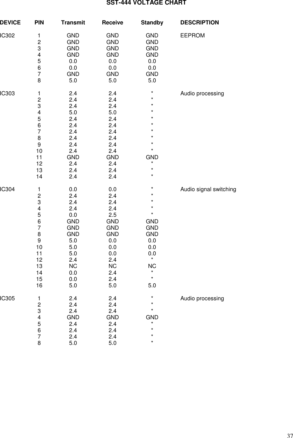
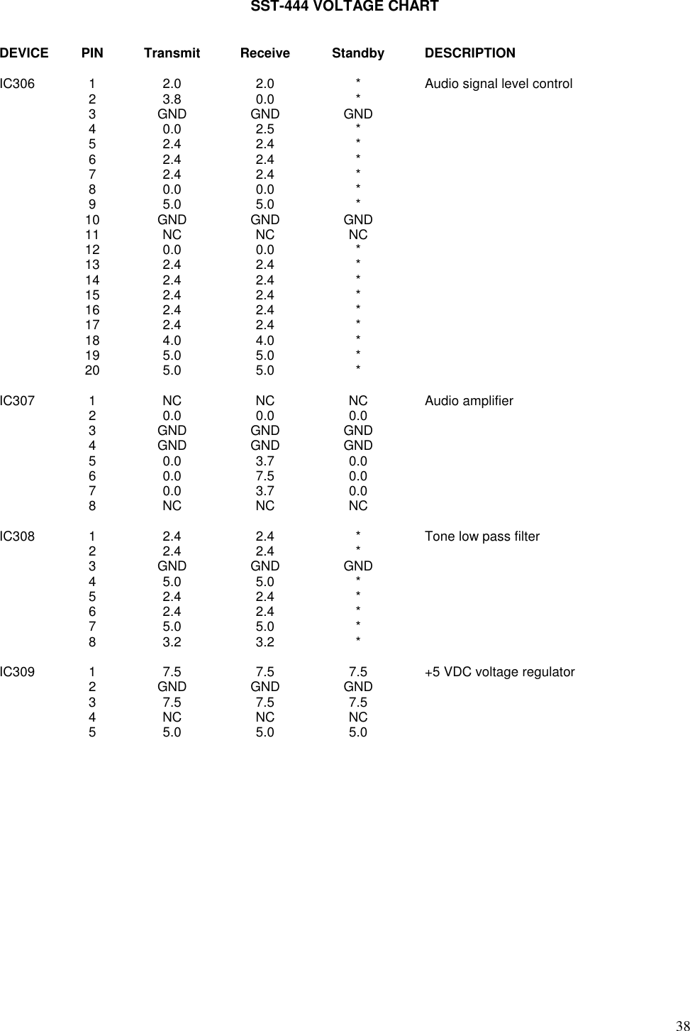
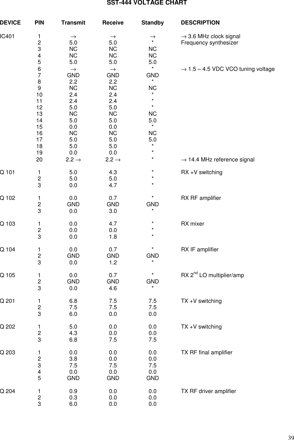
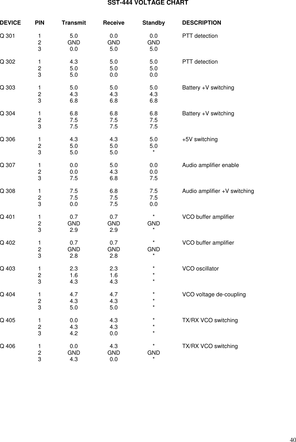
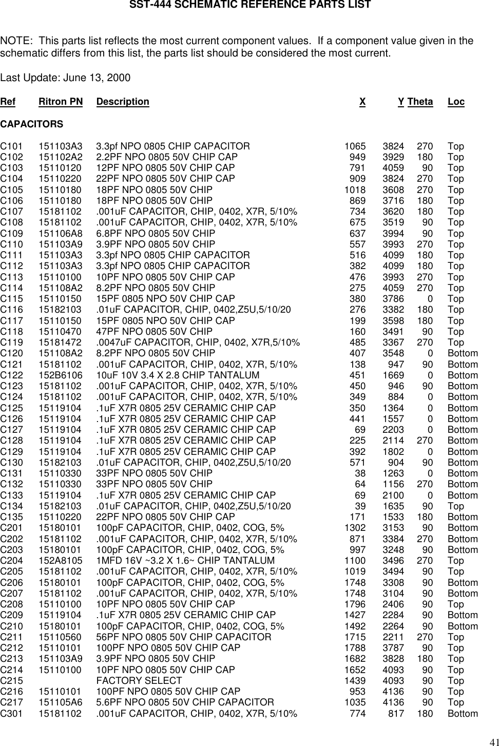
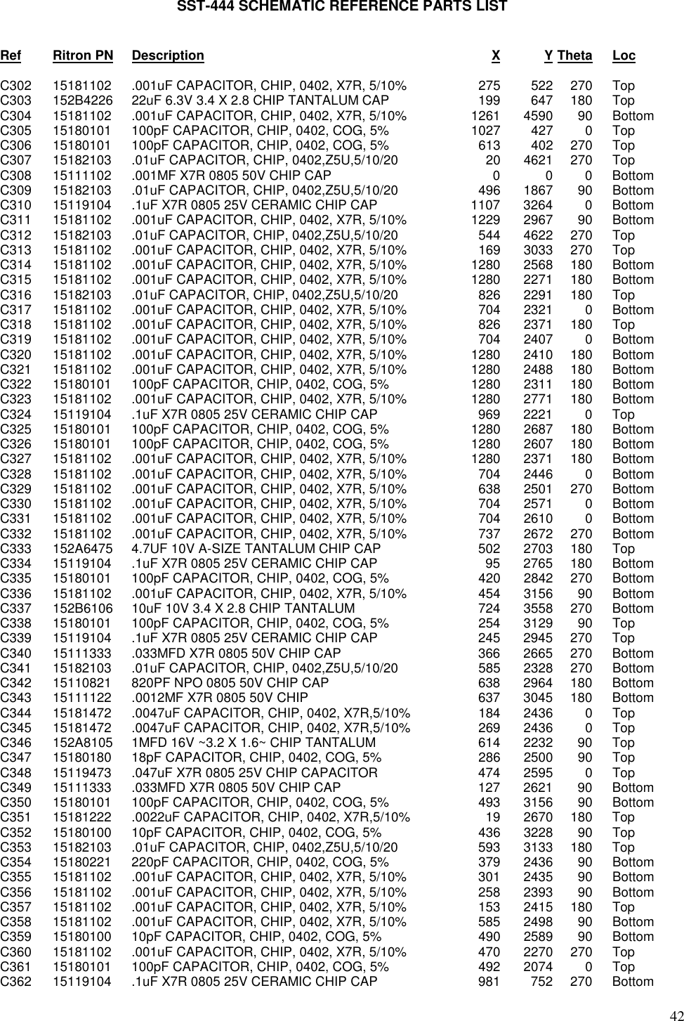
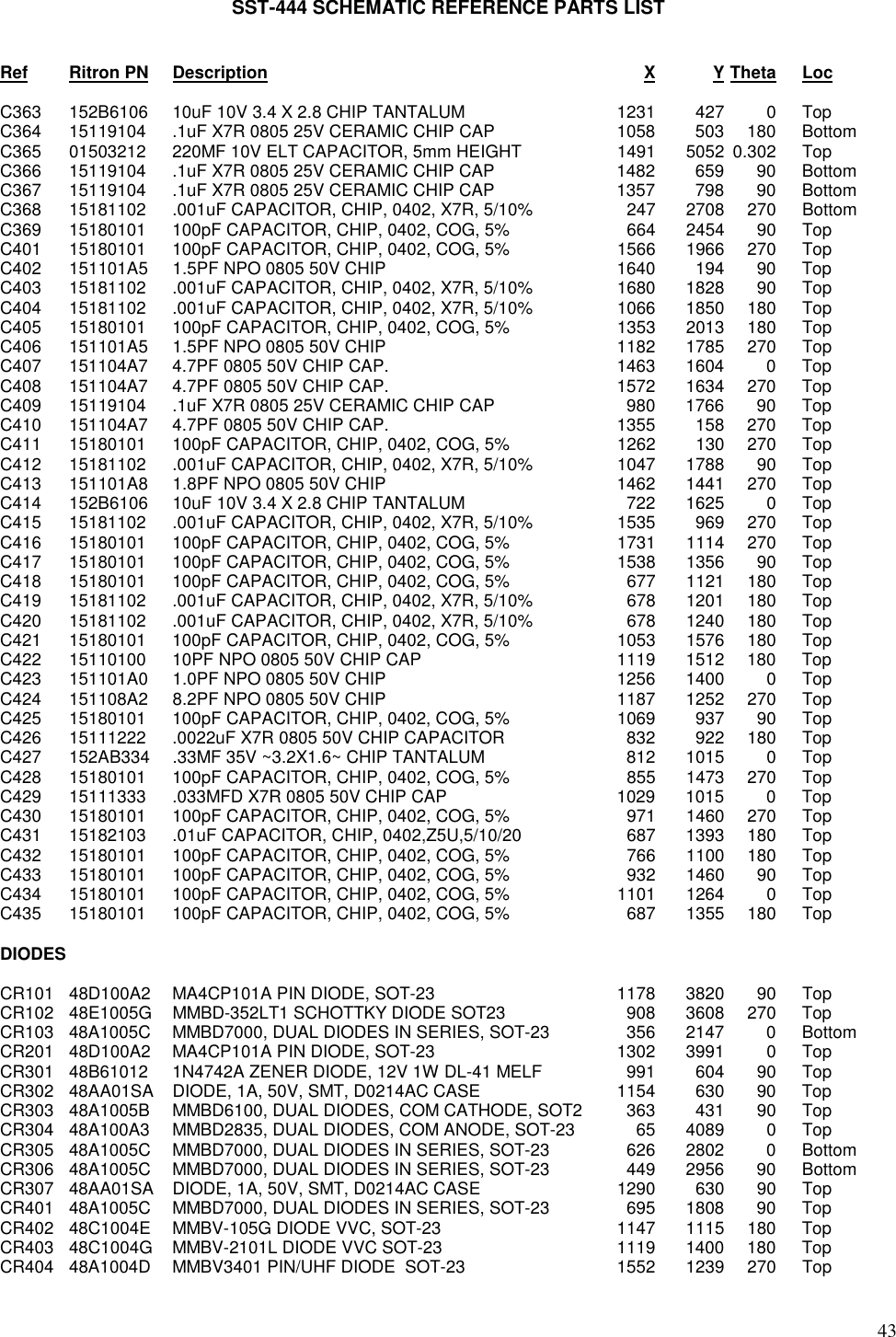
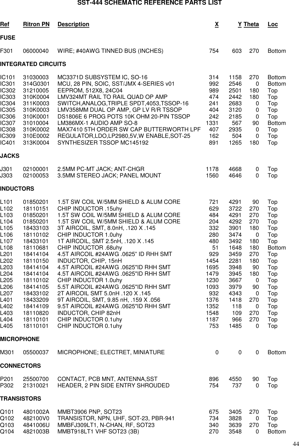
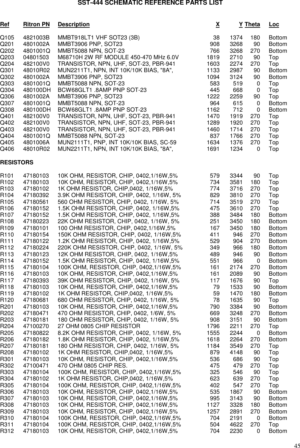
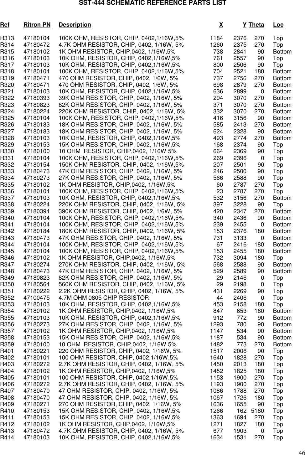
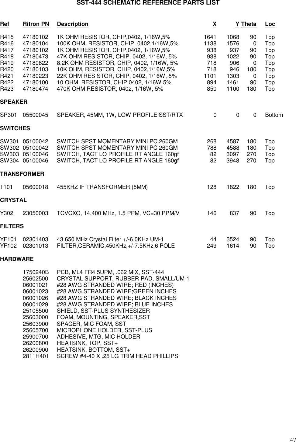
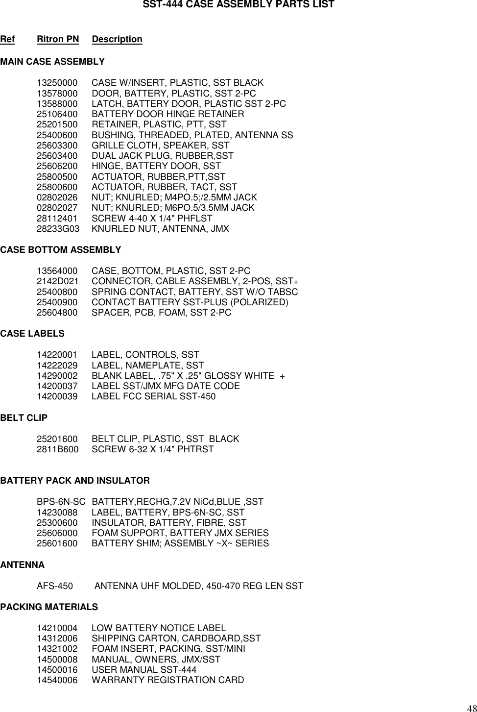
Ritron RIT13-450 UHF-FM Handheld Radio Transceiver User Manual SST 454 THEORY OF OPERATION
Ritron Inc UHF-FM Handheld Radio Transceiver SST 454 THEORY OF OPERATION
UserManual.wiki
>
Ritron
>
RIT13 450 User Manual
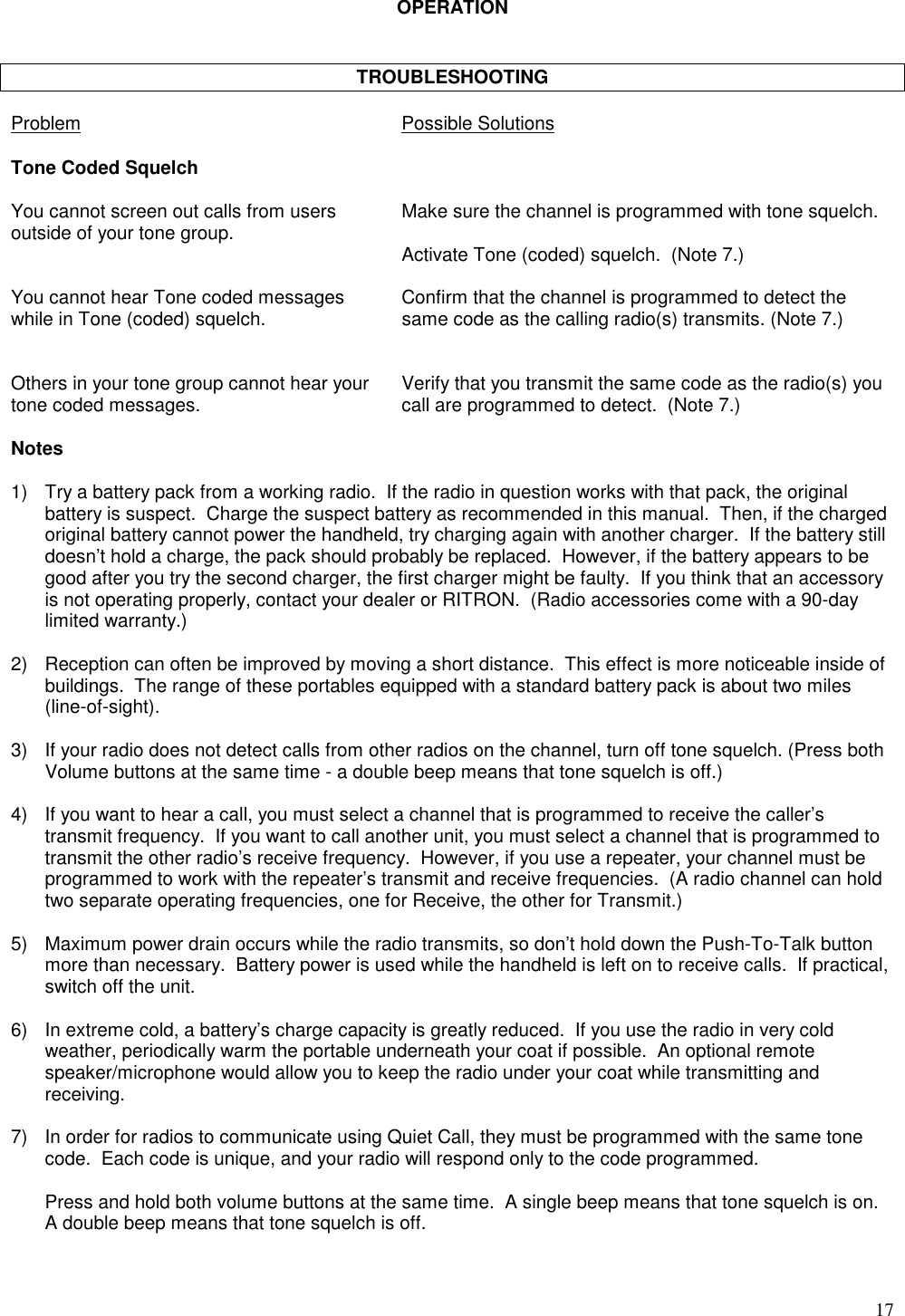
Maintenance manual
Navigation menu
Upload a User Manual
Namespaces
Wiki Guide
HTML
PDF
Info
Views
User Manual
Discussion / Help
Navigation