Ritron RIT15-460 UHF FM Repeater User Manual rlr460man1
Ritron Inc UHF FM Repeater rlr460man1
Ritron >
Contents
- 1. users manual
- 2. Updated Users manual
- 3. Updated Users Manual w GMRS
users manual
TYPE OF EXHIBIT: USERS MANUAL
FCC PART: 2.1033(c)(3)
MANUFACTURER: RITRON, Inc.
505 West Carmel Drive
Carmel, IN 46032
MODEL: RLR-460
TYPE OF UNIT: UHF FM Repeater
FCC ID: AIERIT15-460
DATE: November 25, 2002
Pub. RLR-MRM
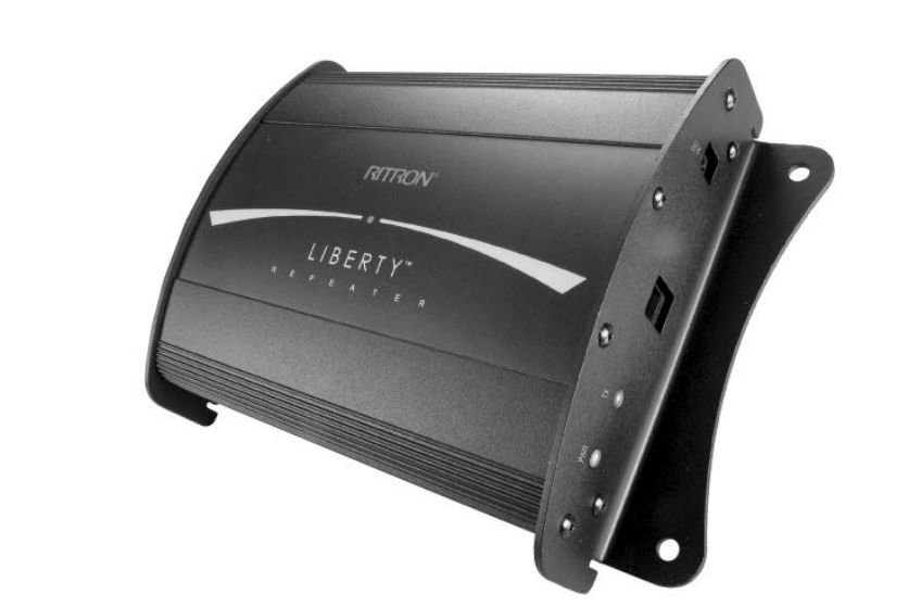
PATRIOT
TWO-WAY RADIO BY RITRON
PROGRAMMABLE FM REPEATER
RLR-460 2/5 Watt UHF
MAINTENANCE/REPAIR/OPERATING MANUAL
FOR USE BY AUTHORIZED SERVICE/MAINTENANCE PERSONNEL ONLY
TABLE OF CONTENTS
1. SPECIFICATIONS
1.1. GENERAL
1.2. RECEIVER
1.3. TRANSMITTER
2. INTRODUCTION
2.1. GENERAL
2.2. INSPECTION
2.3. MODEL IDENTIFICATION
2.4. FCC REGULATIONS
2.5. RF SAFETY ISSUES
3. INSTALLATION
4. OPERATION
4.1. GENERAL
4.2. DUTY CYCLE/TEMPERATURE LIMITS
4.3. INDICATORS
4.4. CONNECTORS
5. PROGRAMMING
5.1. PROGRAMMING SETUP
5.2. COMPUTER SOFTWARE COPYRIGHTS
5.3. PROGRAMMING THE REPEATER
5.4. QUIET-CALL CODES AND FREQUENCIES
5.5. DIGITAL QUIET-CALL CODES
6. ALIGNMENT
6.1. DUPLEXER
6.2. PRELIMINARY
6.3. RECEIVER
6.4. TRANSMITTER
6.5. REGULATOR SUPPLY OPTIONS
6.6. ALIGNMENT POINTS
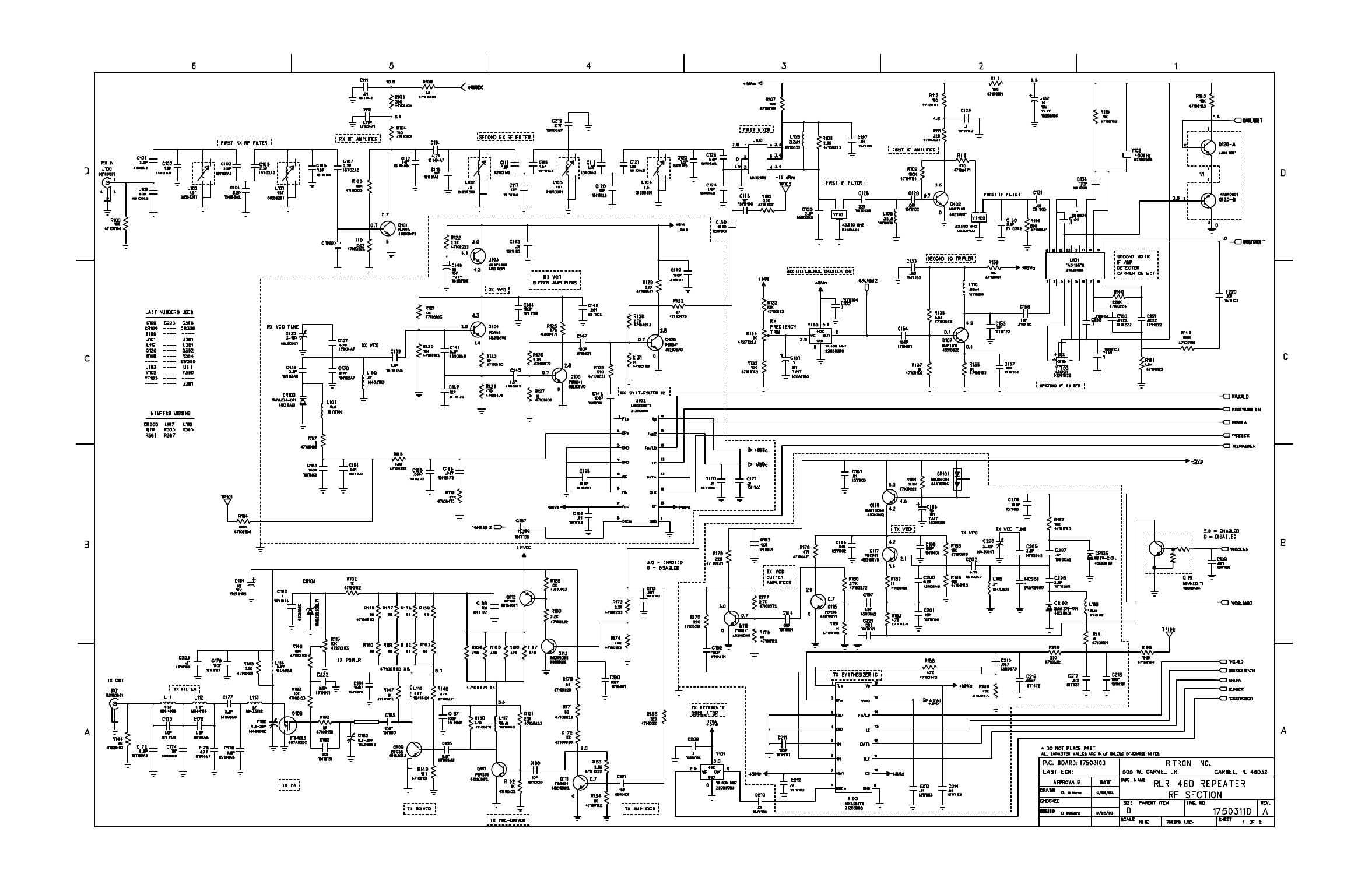
7. THEORY OF OPERATION
7.1. DUPLEXER
7.2. RECEIVER
7.3. TRANSMITTER
7.4. AUDIO
7.5. POWER DISTRIBUTION
7.6. MICROCONTROLLER
8. MAINTENANCE AIDS
8.1. MICROCONTROLLER PIN-OUTS
8.2. CONTROLS AND ADJUSTMENTS SUMMARY
8.3. SCHEMATICS
8.4. PCB COMPONENT LOCATOR
1. SPECIFICATIONS
1.1 GENERAL
Frequency Range 450-470 MHz
FCC ID
RX/TX Separation: 5 MHz
Operational Bandwidth
Duplexer 50 kHz
Receiver and Transmitter 5 MHz
Synthesizer Step Size 12.5 kHz
Channels 1
Power Requirements
2 watt maximum output 12 VDC nominal @ 1A minimum
5 watt maximum output 12 VDC regulated @ 2 A minimum
Tone/Code signaling 1 CTCSS/DCX
Carrier Dropout Timer 0-8 s, programmable by PC
Squelch Tail Timer 0-8 s, programmable by PC
TX Timeout Timer 0-30 min, programmable by PC
Front Panel Connector RJ-12
RF Connector N
Front Panel Indicators 1 Power Green LED
1 TX Red LED
Antenna Impedance 50 ohms resistive, VSWR 1.5:1 or less
Dimensions 8”L x 5.75”W x 2.125” H
Weight 3.5 lbs.
Operating Temperature Range -30°C to +50°C
1.2 RECEIVER 12.5 kHz version 25 kHz version
(At antenna connector)
Sensitivity 0.28 uV 0.28
Adjacent Channel Selectivity 65 dB 75 dB
Spurious Response Rejection 75 dB 75 dB
Image Rejection 80 dB 80 dB
Intermodulation Rejection 70 dB 70 dB
Hum and Noise 45 dB 50 dB
Frequency Stability 1.5 ppm 1.5 ppm
1.3 TRANSMITTER 12.5 kHz version 25 kHz version
(At antenna connector)
Output Power 2/5 watts 2/5 watts
Duty Cycle 100% 100%
Frequency Stability 1.5 ppm 1.5 ppm
Spurious and Harmonics -36 dBm -36 dBm
Hum and Noise 45 dB 50 dB
2. INTRODUCTION
2.1 GENERAL
The RITRON RLR-460 Repeater is a synthesized table-top UHF repeater that operates in the 450 to 470
MHz FM communications band. Its maximum output power level is either 2 watts or 5 watts, depending
upon the type of power supply which is available to power the unit. The unit receives signals originating at
handheld, mobile, or fixed stations on one frequency and simultaneously retransmits the signals on a
second frequency. This type of operation is described as full duplex. The unit contains an integral
duplexer which allows a single antenna to be used for simultaneous transmission and reception. Full
duplex operation with a repeater enables mobile and handheld units to communicate over much greater
distance than is possible without a repeater. The Repeater is designed to be powered from an external DC
power source.
2.2 INSPECTION
Inspect the unit immediately after delivery and report any damages to the shipping company.
2.3 MODEL IDENTIFICATION
The Repeater’s model, serial number, and FCC identification number appear on a label attached to the rear
panel.
2.4 FCC REGULATIONS
The Federal Communications Commission (FCC) requires that the radio owner obtain a station license
before using the equipment to transmit. The user is not required to obtain an operating license. The station
licensee is responsible for proper operation and maintenance of his radio equipment and for ensuring that
transmitter power, frequency, and occupied bandwidth are within the limits specified by the station license.
This is effected by aligning the unit per the instructions in the Alignment section of this manual as well as
periodically checking that transmitter and deviation.
Because the RLR-460 contains a transmitter, THE REPEATER MUST BE LICENSED BEFORE USE. A
RITRON dealer can help with obtaining an FCC license.
2.5 RF SAFETY ISSUES
On August 25, 1997, the FCC adopted the second of two Orders finalizing its rules regarding compliance
with safety limits for human exposure to radio frequency (RF) emissions. All transmitting facilities,
operations and devices regulated by the FCC, including this product, must be in compliance with the RF
exposure limits contained in Code of Federal Regulations (CFR) 47 parts 1.1307(b)(1)-(b)(3). It is the
responsibility of the licensee or grantee to either take action to bring the facility, operation or device into
compliance or file an Environmental Assessment with the FCC. The repeater itself will comply without
any special action. The antenna, however, must be designed and sited in such a way that persons in its
vicinity will not be exposed to RF levels above those specified. In addition, the following precautions
should be taken with regard to the use of this equipment:
This product has been evaluated for compliance with the maximum permissible exposure limits for RF
energy at the maximum power rating of the unit and with the whip antenna available from RITRON. To
ensure compliance with General Population/Uncontrolled maximum exposure limits, all persons must be at
least 20 cm (7.9 inches) from the antenna while the unit is transmitting. Other antennas may require lesser
or greater distances to meet the limits depending upon their gains relative to that tested. Higher gain
antennas are capable of yielding a higher RF energy density in the strongest part of their field and would,
therefore require a greater separation from the antenna.
• DO NOT OPERATE THIS EQUIPMENT unless all RF connectors are secure and any open
connectors are properly terminated.
• GROUND ALL RADIO EQUIPMENT.
• ALLOW ONLY QUALIFIED SERVICE PERSONNEL to service this product.
• DO NOT ALLOW THIS EQUIPMENT to be set to power levels above its design limit or the licensed
maximum.
4. OPERATION
4.1 GENERAL
Test the Repeater for proper operation as the unit is received before attempting to reprogram and/or retune
it. There is no On/Off switch on the unit; it is powered up when a power supply is connected. Standard
factory programming is a receive frequency of 469.500 MHz and a transmit frequency of 464.500 MHz.
Retune the internal duplexer if either the receive or transmit frequency are to be changed by more than 50
kHz. Note that the nominal transmit/receive spacing is 5 MHz for this product. Larger spacings may be
accommodated, but not smaller. See the Alignment section. Retune (re-align) the entire unit if the receive
and/or transmit frequencies are changed by more than 1 MHz. A flashing green LED on the front panel
indicates that the receive voltage controlled oscillator (VCO) is out of lock. In normal operation, the green
LED should glow continuously.
The Repeater is setup to accept a 12 volt/1amp unregulated source of power and can provide up to 2 watts
of output power at the antenna connector. If a source of 12 volts at 2 amperes or greater is available from a
regulated supply, the internal regulator may be bypassed internally and up to 5 watts of output power is
available. See the duty cycle/temperature limits below. The transmitter power output at the antenna
connector can be set internally via a potentiometer to vary from 0.5 watts to the maximum, either 2 watts or
5 watts.
The RLR-460 has a standard frequency separation of 5 MHz between transmit and receive. The normal
configuration is for the receive frequency to be above the transmit frequency. “Inverted” systems are
reversed with the transmit frequency higher than the receive frequency. The cables on the duplexer are
long enough to allow them to be swapped. Normally, the duplexer cables are tie-wrapped in a loop. The
tie-wraps can be cut to allow swapping the connections.
4.2 DUTY CYCLE/TEMPERATURE LIMITS
Due to internal heating of the power supply regulator and the RF transmitter components, there is a limit on
the maximum duty cycle of the Repeater depending upon temperature, output power and whether the
regulator is used. These limits are summarized below:
With internal regulator (Normal Configuration)
Temperature °C Duty Cycle
Output Power 2 watts
25 100 %
50 100 %
Internal regulator bypassed (2A minimum regulated power supply required)
Temperature °C Duty Cycle
Output Power 2 watts
25 100 %
50 100 %
Output Power 5 watts
25 50 %
50 10 %
4.3 INDICATORS
There are two LED indicators, one green and one red, on the front panel. Their operation is detailed below:
Indicator Function Status
Green Power-On Off-Unit not powered-up
Blinking-Receiver Synthesizer Out-of-Lock
Steady On-Normal Operation
Red Transmit Off-Unit not transmitting
Blinking-Transmitter Synthesizer Out-of-Lock
Steady On-Unit Transmitting
Note: If the receiver is out-of-lock (Green LED blinking), the unit will NOT transmit. A synthesizer Out-
of-Lock indication usually means that one or both of the voltage controlled oscillators (VCO’s) needs to be
re-tuned. See the Alignment Section for details on tuning the VCO’s.
4.4 CONNECTORS
There are three connectors on the Repeater; an antenna connector on the rear panel and a DC power
connector and interface connector on the front panel. Their operation is detailed below:
4.4.1 Antenna Connector
One the rear panel is a type N Antenna Connector. An antenna, tuned to a 50 ohm match at the transmit
frequency, should be connected to this connector. Although it is permissible to connect a whip antenna
directly to the connector, best results are usually obtained by using a quarter-wave ground-plane antenna
mounted in an optimum location and connected to the Repeater via a length of low-loss, high quality
coaxial cable. The performance of the duplexer is somewhat dependent on the tuning of the antenna. Whip
antennas are very sensitive to proximity to metal and other surfaces which can make their operation when
directly connected to the Repeater less than optimum.
4.4.2 DC Power Connector
On the right side of the front panel is the DC Power Connector. This connector is a male P-5 type with a
2.11 mm (0.083 in.) inside diameter, 5.51 mm (0.217 in.) outside diameter and a 9.5 mm (0.374 in.)
internal length. The positive terminal is on the outside.
4.4.3 Interface Connector
Near the middle of the front panel is the Interface Connector. This connector is a female telephone RJ-12
modular connector which allows local microphone, speaker, Push-to-Talk and programming connections.
The RITRON Speaker/Microphone sold for use with the Repeater plugs into this connector. The pinout
and description of the pins of this connector are as follows:
Pin No. Name Description
1 GND Circuit ground and common point for other pins.
2 AUDIO IN Pre-emphasized audio input pin. Approximately 25 mV @ 1 kHz
required for 60 % rated maximum deviation. Input impedance
approximately 3 k-ohm.
3 PTT/MIC Combination microphone input and Push-to-Talk input. When the
voltage on this input is taken below approximately 2 volts, the unit
will transmit. This input is also coupled to the transmitter audio
circuitry. When an electret microphone is connected to this input
it is powered by the PTT circuitry and the audio from the microphone
is transmitted.
4 MON When taken to 1 volt or lower, this input over-rides the squelch muting
and allows audio to be present at the AUDIO OUT pin (see below)
even when no signal is present.
5 AUDIO OUT The output of the audio power amplifier. The output level is set by
R330 and it is capable of driving 8-ohm loads.
6 PROG Bi-directional pin for connection to the RITRON programmer.
Note: There is no internal muting on the two audio input pins, AUDIO IN and PTT/MIC. Insure that no
active signal is present on these inputs unless it is desired for that signal to be transmitted.
5. PROGRAMMING
The RLR-460 Repeater may be programmed with a transmit frequency, receive frequency, QC code, DQC
code, and a variety of other features. Some of these other features are:
Transmit time-out timer This feature determines how long the unit may transmit continuously
before the transmitter automatically shuts off.
Tone signaling turn-off time This is the time (in addition to “hang-time” with tone) that no tone
is transmitted after the Repeater ceases to detect an incoming carrier.
Morse code identifier The repeater can be programmed to transmit a Morse code identifier
at a specified time interval after activity.
5.1 PROGRAMMING SETUP
RITRON Programming kit RPT-PCPK supports programming the RLR-460 Repeater using a PC
compatible computer. To use the programming software, connect the Repeater to the computer serial port
with the RITRON adapter cable. Insert the software diskette into the floppy disk drive and load the
software program. The software includes on-screen instructions and Help files. You can also program
added Repeaters identically by saving data to the computer hard drive. It is recommended that the
programming software be copied to the computer hard drive for future programming.
5.1.1 Programming Kit Contents
A. RITRON Repeater Programming Software, complete on one 3.5” diskette.
B. RITRON PC-to-Repeater adapter cable, terminated at one end with a DB-25F connector for
plugging into the computer serial port. The other end terminates in a modular plug, and includes
an adapter for connecting it to the modular jack on the Repeater.
C. Installation instructions.
D. Registration form.
5.1.2 Programming Kit PC Computer Requirements
The computer must run on DOS 3.2 or later, and have an RS-232 serial port available. A hard drive is
recommended.
5.2 COMPUTER SOFTWARE COPYRIGHTS
The RITRON, Inc. products described in this manual include copyrighted RITRON, Inc. computer
programs. Laws in the United States and other countries grant to RITRON, Inc. certain exclusive rights in
its copyrighted computer programs, including the exclusive right to distribute copies of the programs, make
reporductions of the prtgrams, and prepare derivative works based on the programs. Accordingly, any
computer programs contained in RITRON, Inc. products may not be copied or reproduced in any manner
without the express written permission of RITRON. The purchase of RITRON, Inc. products does not
grant any license or rights under the copyrights or other intellectual property of RITRON, Inc., except for
the non-exclusive, royalty-free license to use that arises in the sale of a product, or as adressed in a written
agreement between RITRON, Inc. and the purchaser of RITRON, Inc. products.
5.3 PROGRAMMING THE REPEATER
1. Remove power from the Repeater.
2. Insert the programming cable into the RJ-12 jack on the front of the Repeater.
3. Start the programming software and follow the on-screen instructions.
4. Insert “R” on the main software screen to return to normal operating mode.
5.4 QUIET-CALL CODES AND FREQUENCIES
QC Tone Freq. QC Tone Freq. QC Tone Freq.
Code Code (Hz) Code Code (Hz) Code Code (Hz)
01 XZ 67.0 18 3Z 123.0 35 M4 225.7
02 XA 71.9 19 3A 127.3 36 --- 233.6
03 WA 74.4 20 3B 131.8 37 --- 241.8
04 XB 77.0 21 4Z 136.5 38 --- 250.3
05 SP 79.7 22 4A 141.3 39 --- 69.4
06 YZ 82.5 23 4B 146.2 40 --- 159.8
07 YA 85.4 24 5Z 151.4 41 --- 165.5
08 YB 88.5 25 5A 156.7 42 --- 171.3
09 ZZ 91.5 26 5B 162.2 43 --- 177.3
10 ZA 94.8 27 6Z 167.9 44 --- -----
11 ZB 97.4 28 6A 173.8 45 --- 183.5
12 1Z 100.0 29 6B 179.9 46 --- 189.9
13 1A 103.5 30 7Z 186.2 47 --- 196.6
14 1B 107.2 31 7A 192.8 48 --- 199.5
15 2X 110.9 32 M1 203.5 49 --- 206.5
16 2A 114.8 33 M2 210.7 50 --- 229.1
17 2B 118.8 34 M3 218.1 51 --- 254.1
53 --- Custom
5.5 DIGITAL QUIET-CALL CODES
Normal Invert Normal Invert Normal Invert Normal Invert
023 047 143 412 315 423 532 343
025 244 152 115 331 465 546 132
026 464 155 731 343 532 565 103
031 627 156 265 346 612 606 631
032 051 162 503 351 243 612 346
043 445 165 251 364 131 624 632
047 023 172 036 365 125 627 031
051 032 174 074 371 734 631 606
054 413 205 263 411 226 632 624
065 271 223 134 412 143 654 743
071 306 226 411 413 054 662 466
072 245 243 351 423 315 664 311
073 506 244 025 431 723 703 565
074 174 245 072 432 516 712 114
114 712 251 165 445 043 723 431
115 152 261 732 464 026 731 155
116 754 263 205 465 331 732 261
125 365 265 156 466 662 734 371
131 364 271 065 503 162 743 654
132 546 306 071 506 073 754 116
134 223 311 664 516 432
6. ALIGNMENT
6.1 DUPLEXER
The duplexer allows the Repeater to simultaneously transmit and receive. To accomplish this, in the
receive input path, the transmitter signal must be notched or suppressed by 70 dB or more. In addition, on
the transmit path, transmitter noise on the receive frequency must be also suppressed by about 70 dB. The
duplexer contains four cavities, two for each path to achieve the necessary notch depth. Because the
notches are very narrow, the duplexer must be re-tuned if the frequency of operation is changed by more
than 50 kHz. Follow the procedure below to tune the duplexer:
1. Connect the antenna to be used to the antenna connector on the Repeater. If possible, the antenna
should be positioned in a way that matches the actual configuration as close as possible. If the antenna
requires tuning, tune it to the transmit frequency. If an antenna is not available, connect a low VSWR
50-ohm load instead.
2. Unplug the two RF cables connecting the duplexer to the main PCB.
3. A spectrum analyzer with tracking generator or a network analyzer should be used to sweep the
duplexer. If one is not available, a spectrum analyzer and an RF signal generator can be used, but the
notch frequencies will be difficult to determine. The duplexer should be swept from one RCA plug to
the other; it doesn’t matter which end goes to the generator or the spectrum analyzer.
4. One should see at least two, and maybe as many as four notches. Carefully loosen the nuts on the two
duplexer cavities underneath the transmitter portion of the main PCB. Adjust the two cavity screws for
the deepest notch possible at the RECEIVE frequency. Tighten the nuts being careful not to de-tune
the notch frequency. Do the same for the two screws on the cavities underneath the receiver portion of
the main PCB, but tune for a notch at the TRANSMIT frequency. When finished, one should see two
notches, one at the transmit frequency and one at the receive frequency. These two notches are very
narrow and special attention should be paid to ensuring that they are at the correct frequencies. The
two notches should be about 70 dB deep compared to a straight-through connection.
6.2 PRELIMINARY
1. Alignment of the RLR-460 Repeater requires that surface-mount potentiometers be adjusted. These
potentiometers do not have end stops so one must pay special attention to the wiper position for
maximum clockwise and counterclockwise settings. Also, one should be careful never to set the wiper
in the dead band between maximum and minimum.
2. Alignment of the Repeater requires connection to the pins on the front panel modular jack.
3. The frequency deviation numbers shown are for narrow (12.5 kHz channel spacing) operation. Double
the values for wide (25 kHz channel spacing) operation.
4. A communications service monitor capable of duplex operation is required to set R328 (REPEAT
AUDIO LEVEL). Other alignment steps can use individual pieces of equipment (RF signal generator,
RF wattmeter, etc.), although communications service monitors tend to include all the functions
necessary to align this product.
5. Ensure that the Repeater is properly programmed for the correct transmit and receive frequencies and
the correct QC/DQC tones/codes. Even if a transmit tone is not to be used (unusual), one should
program one anyway to get the transmit tone deviation properly set. This parameter is, however, set at
the factory.
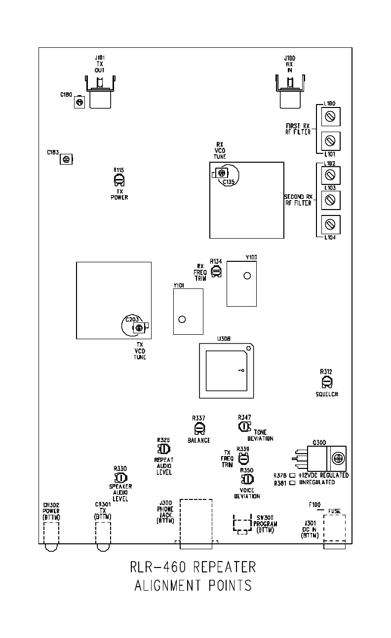
6. Refer to the RLR-460 ALIGNMENT POINTS diagram for the location of alignment points and
adjstments.
6.3 RECEIVER
1. Apply power to the Repeater. The green front panel LED should be illuminated, but may be blinking.
2. Connect the MON input (modular jack pin 4) to ground (modular jack pin 1). This will override the
squelch operation and also inhibit the transmitter.
6.3.1 Local Oscillator Trim
1. Connect a test probe from a frequency counter or frequency measuring device to test point TP103. The
receiver 1st local oscillator signal at approximately –12 dBm is present at this point. The correct
frequency at this point is the receive frequency minus the 1st IF frequency of 43.65 MHz (fLO = fRX -
43.65).
2. Using a tuning tool, adjust R134 (RX FREQ TRIM) for the correct frequency +/-100 Hz.
6.3.2 Receive VCO Tuning
1. Connect a high impedance oscilloscope probe to an oscilloscope set for 1 V/div, DC coupled. The
sweep speed is not important.
2. Connect the ground lead of the probe to the PCB ground. The mounting legs of the receiver input
connector J100 can be used. Touch the probe tip to TP100 and note the voltage on the oscilloscope.
This point is very sensitive and the synthesizer may go out of lock. This will be evident by an initial
voltage which then decays to zero in about a few seconds. Note the voltage right after the probe is
touched to the test point and before it begins decaying.
3. Using an insulated tuning tool, adjust C135 inside the VCO/synthesizer (RX VCO TUNE) shield for
2.5 +/-0.25 volts at TP100. The green front panel LED should be illuminated continuously (not
blinking).
6.3.3 Receiver Front-End Tuning
1. Connect a SINAD meter to the AUDIO OUT output (pin 5). Set R330 (SPEAKER AUDIO LEVEL)
to mid rotation.
2. Connect an RF signal generator to the antenna connector. The generator frequency should be set to the
desired receive frequency modulated with a 1 kHz tone at 1.5 kHz deviation. The RF level should be
set to 7 uV (–90 dBm).
3. If the SINAD meter reads greater than 12 dB, reduce the RF signal generator output level until 12 dB
SINAD is reached. Adjust L100 through L104 for best SINAD while reducing the RF signal generator
output level to keep the SINAD near 12 dB. The RF outptut level for 12 dB SINAD should be 0.25 uV
(-119 dBm) or less.
6.3.4 Squelch
1. Set the RF signal generator output level to produce a SINAD where the squelch is desired to unmute,
typically 12-14 dB.
2. Rotate R312 (SQUELCH) to the maximum clockwise point. Connect an oscilloscope probe to TP104.
The voltage at TP104 should be 5 VDC. Adjust R312 counterclockwise until the TP104 voltage drops
to zero. Then, slowly adjust R312 clockwise to the point where the TP104 voltage again goes to 5
volts.
6.3.5 Audio Output Level
1. Increase the RF signal generator output level to 7 uV (-90 dBm). The SINAD reading should be close
to 20 dB or so. Connect an oscilloscope to the AUDIO OUT (pin 5) on the modular jack. The SINAD
meter is already connected to this point.
2. Adjust R330 (SPEAKER AUDIO LEVEL) for the desired output level.
6.4 TRANSMITTER
1. Apply power to the Repeater.
2. Set R115 (TX POWER) to the full counterclockwise position. This is the minimum power point.
3. Connect a 50-ohm RF dummy load capable of handling 5 watts to the Antenna connector. Provisions
should be made to couple the RF output signal to a demodulator, a frequency counter, and an RF
wattmeter. The demodulated output must be viewable on an oscilloscope.
4. The transmitter will be keyed by taking pin 3 of the modular jack (PTT/MIC) to ground.
5. Ensure that the signal generator output of the service monitor is set to a very low level to prevent the
receive squelch from unmuting. This will prevent the transmitter from keying due to receiving a valid
carrier. Having a receive QC/DQC tone/code programmed will help greatly in preventing nuisance
keying.
6.4.1 Transmit VCO Tuning
1. Connect a high impedance oscilloscope probe to an oscilloscope set for 1 V/div, DC coupled. The
sweep speed is not important.
2. Connect the ground lead of the probe to the PCB ground. The mounting legs of the transmitter output
connector J101 can be used. Key the transmitter, touch the probe tip to TP101 and note the voltage on
the oscilloscope. This point is very sensitive and the synthesizer may go out of lock. This will be
evident by an initial voltage which then decays to zero in about a few seconds. Note the voltage right
after the probe is touched to the test point and before it begins decaying.
3. Using an insulated tuning tool, adjust C203 inside the VCO/synthesizer shield (TX VCO TUNE) for
2.5 +/-0.25 volts at TP101. The red front panel LED should be illuminated continuously (not
blinking). Unkey the transmitter.
6.4.2 Transmitter Output Power
1. Key the transmitter and not the output power. Adjust C180 and C183 for maximum output power. If
the output power is too low, adjust R115 (TX POWER) clockwise about 45 ° and readjust C180 and
C183. Adjust R115, C180, and C183 until the desired output power is reached. For 2 watts, R115
would typically be at mid-rotation and for 5 watts, near 80% rotation.
2. Unkey the transmitter.
6.4.3 Modulation Balance and Deviation
1. An audio generator should be connected to the AUDIO IN (pin 2) input of the modular jack. The
audio frequency should be 500 Hz and the level should be 10 mV rms or lower.
2. Set R347 (TONE DEVIATION) to the full counterclockwise position.
3. To RF output should be routed to an FM demodulator and the demodulated output made viable on an
oscilloscope. The filtering on the demodulator should be 15 kHz or higher on the lowpass filter and
below 50 Hz on the highpass filter.
4. While observing the oscilloscope, key the transmitter. Increase the audio generator level until the 500
Hz sinewave becomes viable on the oscilloscope. Increase the generator level until a significant
amount of clipping on the top and bottom of the sinewave is evident.
5. Carefully adjust R337 (BALANCE) so that the clipped portion of the observed waveform is flat i.e. not
tilted up or down.
6. Adjust R350 (VOICE DEVIATION) for +/- 2.35 kHz deviation.
7. Unkey the transmitter.
6.4.4 Transmitter Frequency Trim
1. Remove the audio generator connection.
2. Key the transmitter and note the frequency of the RF output signal. Adjust R339 (TX FREQ TRIM)
for the correct transmit frequency +/- 100 Hz.
Unkey the transmitter.
6.4.5 Tone Deviation
1. Key the transmitter and adjust R347 (TONE DEVIATION) for the desired tone/code deviation,
typically 350 Hz.
2. Unkey the transmitter.
6.4.6 Repeat Audio Level
1. For this adjustment, the service monitor must be able to generate an RF signal and simultaneously
demodulate an incoming RF signal.
2. Set the RF signal generator for the correct receive frequency with 1.5 kHz deviation of a 1 kHz tone
and modulated with the correct tone/code, if used. The RF output level should be set for 7 uV (-90
dBm) The demodulator should be set to display deviation.
3. The transmitter should automatically key (red LED illuminated). Adjust R328 (REPEAT AUDIO
LEVEL) for +/- 1.5 kHz deviation.
4. Reduce the RF signal generator level to minimum to unkey the transmitter.
6.5 INTERNAL REGULATOR OPTIONS
An internal voltage regulator exists in the RLR-460 repeater to regulate the DC input voltage to that
required by the transmitter stages. If a regulated power supply is available, this internal regulator may be
bypassed. Bypassing the internal regulator allows for a higher RF output power. A more complete
description of the regulator options follows:
When the Repeater is used with an unregulated power supply, wide fluctuations in voltage and large AC
ripple content are common. Both must be removed for proper operation. This is effected by the internal
voltage regulator. The internal regulator does, however, generate heat which limits the maximum current
which can be passed through the regulator and to the transmitter power amplifier. This in turn limits the
maximum output power to 2 watts even if the power supply is capable of the required current. To use the
internal regulator, R378 should be installed. This is the normal configuration of the Repeater as set at the
factory and is the configuration for use with the RITRON RPS-1A power supply.
If a regulated power supply is used, the internal regulator may be bypassed to allow higher current
operation and thus greater output power to 5 watts. To effect this change, move the resistor in the R378
pad pair to R381 which is next to it. Note that a regulated supply can be used with the Repeater set for
internal regulation, but the maximum RF output power is still limited to 2 watts.
7. THEORY OF OPERATION
7.1 DUPLEXER
The duplexer allows for simultaneous transmission and reception of RF signals. There is a receive path and
a transmit path which connect to the RF input and output of the main PCB and a common point at the
antenna connector.
In the receive path is a two-cavity notch filter. This filter allows the receive signal from the antenna
connector to pass through with about 1.5 dB loss, but notches the transmitter RF output signal by 70 dB or
more to prevent overloading the receiver. The transmit path also contains a two-cavity notch filter, this one
tuned to the receive frequency. This filter removes transmitter noise which exists at the receive frequency
and which would interfere with the desired receive signal, if not removed.
7.2 RECEIVER
7.2.1 Front-End
The receiver front-end comprises the RF amplifier stages with associated filters and the first mixer. The
input signal from the J100 (RX IN) passes through a two-pole bandpass filter formed around L100 and
L101. This filter is narrow enough at 10 MHz to protect the receive RF amplifier, but wide enough to keep
its insertion loss low at 2.3 dB. This filter stage is followed by the RF amplifier. The RF amplifier stage
has a gain of about 12 dB and a noise figure of 1.5 dB. This stage, along with the first filter, are largely
responsible for the sensitivity of the Repeater. The RF amplifier is followed by a three-pole bandpass filter
formed around L102 through L104. This filter is somewhat narrower than the two-pole filter and thus has a
higher insertion loss at 4 dB. The total filtering action is to limit the number of off-channel interfering
signals that the receiver might be exposed to and to remove signals at the spurious response frequencies of
the mixer which follows.
The job of the 1st mixer, U100 is to convert signals at the receive frequency to that of the 1st IF at 43.65
MHz. It does this by mixing the 1st local oscillator signal at a frequency 43.65 MHz below that of the
desired receive frequency to the IF frequency of 43.65 MHz. The 43.65 MHz output of U100 exits at pin 4
and is routed to the 1st IF filter. U100 has a conversion gain of 12 dB and a noise figure of 6 dB. This
performance in combination with the front-end RF amplifier stage determines the sensitivity of the
receiver.
7.2.2 1st IF
The 1st IF stage consists of two two-pole monolithic crystal filters separated by an amplifier. The two
filters are YF101 and YF102. These filters are bandpass in response with a bandwidth of 12 kHz and an
insertion loss of 1.5 dB. To overcome the losses of the filters and to prevent interaction between them, they
are separated by an amplifier formed around Q102.
7.2.3 2nd IF Sub-System
IC U101 is responsible for converting signals at the 1st IF to the 2nd IF where additional filtering and
amplification take place. The 43.65 MHz signals enters U101 at pin 16. It is then mixed with the 2nd local
oscillator signal at pin 1 to product a signal at the 2nd IF of 450 kHz at pin 3. The 2nd IF signal at pin 4 is
filtered by the YF103, the 2nd IF filter. This filter is a bandpass filter with a bandwidth of 7.5 kHz and an
insertion loss of 5 dB. The output of the filter re-enters U101 at pin 5 where it is amplified and then limited
to remove amplitude modulation components. The limited signal is then mixed against a 90° phase shifted
version of itself and filtered by Y102. This acts as an FM demodulator. The demodulated output exits
U101 at pin 9.
U101 also provides for squelch operation. The presence of a carrier is sensed by noting that ultrasonic
noise on the demodulated output decreases when a carrier is present. An amplifier between pins 7 and 8 of
U101 and associated external parts form an audio bandpass filter at 3.5 kHz. The output of this filter is
internally rectified and exits at pin 14. This signal pass through a temperature compensation network
formed around both halves of Q120. The result is a signal whose DC level drops with increasing carrier
level.
7.2.4 1ST Local Oscillator/Receive Synthesizer
The local oscillator signal for the 1st mixer is generated by the receive synthesizer. The receive synthesizer
is based around a voltage controlled oscillator (VCO) and a synthesizer sub-system IC which handles the
digital portion of the synthesizer. The voltage controlled oscillator is an oscillator whose frequency can be
controlled by a voltage. The receive voltage controlled oscillator is formed around Q104 with varactor
diode CR100 electronically controlling the frequency. A sample of the oscillator frequency is sampled by
R128 and C148 and sent to U102, an integrated monolithic Phase-Locked Loop (PLL) synthesizer IC.
Inside U102, the VCO frequency is divided by programmable digital dividers to 12.5 kHz. Y100, the 14.4
MHz receive reference oscillator’s frequency is also divided down to 12.5 kHz. A phase/frequency
detector compares the two divided down frequencies and generates an error signal at U102, pin 2 which is
filtered and used to pull the VCO on frequency. By controlling the VCO divider number, the locked
frequency can be changed in 12.5 kHz steps. The divider numbers are loaded into U102 by the
microprocessor. The tuning range of the VCO is set by C135. Because the VCO is locked to the receive
reference oscillator, Y100, the frequency stability of Y100 determines the frequency stability of the VCO
and thus the 1st local oscillator.
The output of the VCO is amplified by Q105 and Q106 to about 0 dBm to drive the 1st mixer. For
alignment purposes, a sample of the 1st local oscillator is available at TP103. For proper mixing operation,
the VCO is made to oscillate at a frequency 43.65 MHz below the receive frequency.
7.2.5 2ND Local Oscillator
To convert the 1st IF signals at 43.65 MHz to the 2nd IF frequency of 450 kHz, requires a 2nd local oscillator
frequency of 43.2 MHz (43.65 – 0.450). This is created by multiplying the 14.4 MHz output frequency of
Y100 by three in Q107.
7.3 TRANSMITTER
7.3.1 Transmit Synthesizer
The transmit synthesizer operates similar to the receive synthesizer except that the oscillator is locked to
the transmit frequency rather than offset by the 1st IF frequency. The transmit VCO is formed around Q117
and electronically tuned by CR102. The oscillator frequency is sampled by R175 and C192 and routed to
U103, the transmit synthesizer IC. The oscillator frequency is divided down to 12.5 kHz and compared in
phase and frequency to the divided transmit reference oscillator signal. The error signal is filtered and sent
to the varactor diode CR102 to lock the VCO on frequency. The 12.5 kHz reference is created by dividing
down the transmit reference oscillator frequency of 14.4 MHz from Y101. To modulate the transmitter, the
VCO must allow for frequency modulation other than what is required to put it on frequency. This is
effected by DR103. The tuning range of the VCO is set by C203. Q119 is an electronic switch which
keeps the transmit VCO turned off when the unit is not transmitting.
7.3.2 RF Power Amplifier Stages
The output of the VCO buffer stage, Q114 is at a level of about 0 dBm. This is amplified to the 2 to 5 watt
level by Q111, Q110, Q109, and Q108. Q112 and Q113 are electronic switches which only allow the
amplifier stages to be turned on after the transmit VCO is locked and on frequency. The output power can
be adjusted by R115, which set the bias voltage on the final power stage. Q108 is followed by an
impedance matching network and a low-pass filter to remove transmitter frequency harmonics.
7.4 AUDIO
7.4.1 Receiver
Discriminator audio from U101 passes to U301-A where it is buffered and then sent to the tone signaling
filter and the voice highpass filter. U302, a 5-pole switched capacitor low-pass filter is used to remove
voice and other components from the discriminator audio and leave only signaling tones. The output
passes to comparator U300-A where it is converted to square waves for the microcontroller. U301-B and
U301-C are used to form a 6-pole high-pass filter which removes signaling tones from the voice audio
signal. Its output is routed through two analog switches and then to the audio power amplifier and to the
transmit audio chain.
U300-B is the squelch comparator. This IC compares the DC voltage from the carrier detect circuits of
U101 to the squelch setting and generates a logic output which represents the state of the carrier detection
circuitry. Squelch hysteresis, to prevent chattering, is provided by R313.
7.4.2 Transmitter
Audio input signals from J300 are amplified by U305-A and then fed through the pre-emphasis network
R356 and C339 to the modulation limiter. The modulation limiter is formed around U305-B which is an
op-amp that can clip against its supply rails in a controlled manner. Also summed into the input of the
clipper are the audio from the receiver to be transmitted and the Morse code ID tone from the
microprocessor. The output of the limiter is fed through a 5-pole low-pass filter which removes audio
harmonics caused by the modulation limiting. Signaling tones are also added at this point. The output of
the limiter filter is passed to the transmit VCO and also the transmit reference oscillator. Sending the
filtered transmit audio to both ensures that the transmitter audio frequency is flat to DC.
7.5 POWER DISTRIBUTION
DC supply voltage for the Repeater enters the unit at J301. If the internal regulator is to be used, R381 will
be installed. The internal regulator is formed around pass transistor Q300 and a zener voltage reference,
CR306. This regulator nominally regulates to 11 volts from a 12 volt or higher source. If the voltage falls
below 12 volts, the regulator will no longer regulate, but will filter the incoming source. If R378 is
installed, the regulator is bypassed. The incoming source is used to power directly the RF power amplifier
and driver stages of the transmitter. For the digital portions of the Repeater, a 5-volt regulator, U310 is
provided. The audio circuits are powered from U311, a low noise, high precision 5-volt regulator.
7.6 MICROCONTROLLER
U308 is the microcontroller which controls the operation of the Repeater. Its internal clock is controlled by
Y300, a 4 MHz crystal. U309 is a non-volatile memory IC used to store frequency, tone, and control
information. This information is retained even when the Repeater is powered down.
8.0 MAINTENANCE AIDS
8.1 MICROCONTROLLER PIN-OUTS
The pin-outs and description for U308, the microprocessor follow. Note that a logic low (0) is a voltage
below 0.5 volts while a logic high (1) is a voltage above 3.5 volts.
Pin 1 RESET
Active low pin used to place the microcontroller in the reset state. This pin is driven by U307, a
commercial microprocessor supervisory IC which is designed to go low after power supply voltage glitches
and power-up. Normal state for this pin is logic high.
Pin 2 IRQ
Active low external interrupt input. When this pin goes low, the microcontroller jumps to a pre-determined
internal software subroutine. This pin is tied to the PTT input. Normal state is high except when driven
low by an external PTT signal at J300, pin 3.
Pin 3 NC
Not used.
Pin 4 Vpp
Programming power supply pin. Not used once the part is in the Repeater.
Pin 5 TX TONE
This output is the signaling tone to be transmitted. For QC, it is a square wave at the tone frequency. For
DQC, it is the unfiltered DQC waveform.
Pin 6 TX TONE SHIFT
This output controls the corner frequency of the transmitter tone filter, U306. It shift between open circuit
(tri-state) when the corner frequency is to be high to low when the corner frequency is to be shifted
downward for the lower set of QC tones.
Pin 7 RX TONE SHIFT
This output controls the corner frequency of the receiver tone filter, U302. It shift between open circuit (tri-
state) when the corner frequency is to be high to low when the corner frequency is to be shifted downward
for the lower set of QC tones.
Pin 8 VCO EN
This output enables the transmit VCO. This pin is high when the VCO is to be enabled in order for the
repeater to transmit and low otherwise.
Pin 9 TX PA EN
This output enables the last three transmitter power amplifier stages. This pin goes low to enable these
stages when the Repeater is to transmit and high otherwise. This pin would normally go low about 20 ms
after pin 8 above goes high when transmit is initiated.
Pin 10 RX TONE
This input is the square wave from the receive tone filter and comparator, U300-A. This waveform would
normally be a square wave version of a received QC or DQC tone/signal.
Pin 11 SPKR EN
This output enables the audio gate which drives the audio PA for speaker audio. It is active low when
speaker audio is to be present.
Pin 12 REPEAT AUDIO EN
This output enables the audio gate which routes receive voice audio to the transmit audio chain. It is active
low when audio is to be routed to the transmitter.
Pins 13, 14 Not Used
Pin 15 BEEP/ID TONE LSB
This output is the least significant bit of a two bit output for generating tones to be transmitted.
Pin 16 EEPROM Enable
This output is used to control the U309, the memory IC.
Pins 17, 18 SQUELCH
This input is the output of U300-B. It is high when a valid carrier is detected. Note that this input
considers only the presence of a carrier, not whether the correct signaling tone is present.
Pin 19 MON
This input is from J300, pin 4 and is low when it is desired to have speaker audio present. The unit will not
transmit when this input is taken low, even if a valid signal is received or the PTT line is taken low.
Pin 20 RX LD
This input is the receiver synthesizer lock detect output. It is high when the receive synthesizer is in lock.
Pin 21 TX LD
This input is the transmit synthesizer lock detect output. It is high when the transmit synthesizer is in lock.
This would be the normal state for transmit, but this input should be low otherwise.
Pin 22 GROUND
Pin 23 Not Connected
Pin 24 DATA
This output is the data line from the microcontroller to the various peripherals in the Repeater, including
the memory IC and the synthesizer IC’s.
Pin 25 TX SYN EN
This output enables the transmitter synthesizer IC, U103 to receive data from the microprocessor. This pin
will change states when the transmitter synthesizer is to be loaded. This would occur just before the
Repeater is to transmit.
Pin 26 RX SYN EN
This output enables the receiver synthesizer IC, U102 to receive data from the microprocessor. This pin
will change states when the receive synthesizer is to be loaded. This would occur just after microprocessor
reset.
Pin 27 CLOCK
This output is the clock line from the microprocessor to the various peripherals in the Repeater, including
the memory IC and the synthesizer IC’s.
Pin 28 EEPROM DATA
This input/output is the data line to and from the memory IC, U309.
Pin 29 BEEP/ID TONE MSB
This output is the most significant bit of a two bit output for generating tones to be transmitted.
Pin 30 POWER LED
This active low output drives the power (green) front panel LED.
Pin 31 TX LED
This active low output drives the transmit (red) front panel LED.
Pins 32, 33 PROG
This input/output is used to communicate with the external programmer.
Pin 34 PROGRAM
This input puts the microcontroller into a special programming mode. Not used in all models.
Pins 35-38 Not Used
Pins 39, 40 Connected together, but not used
Pin 41 Not Used
Pins 42, 43 OSC1, OSC2
These two pins support the external crystal for generating the internal microprocessor clock.
Pin 44 Vdd
This is the 5-volt supply pin for the microprocessor. Normal voltage is 5 volts when powered up.
8.2 CONTROLS AND ADJUSTMENTS SUMMARY
Below is a summary of the controls and adjustments on the Repeater. Most, if not all, are covered in the
alignment section, but are included here for reference.
L100-L104
These are the adjustable front-end bandpass filter inductors. Since the front-end has a bandwidth of about
7-8 MHz, these should be re-adjusted when the receive frequency is moved by 1 MHz or more. Turning
the slugs clockwise tunes the filter higher in frequency. A non-metallic tuning tool should be used.
C135 RX VCO TUNE
This is a trimmer capacitor inside the receive synthesizer/VCO shield. It is accessible via a hole in the top
of the shield. This trimmer adjusts the tuning range of the receive so that it is centered around the receive
frequency. It is typically re-adjusted when the receive frequency is changed by more than 1 MHz.
R134 RX FREQ TRIM
This potentiometer trims the receive reference oscillator to the correct frequency. It is typically adjusted
while observing the frequency at TP103. There are no stops on this potentiometer and one must avoid the
dead band between the maximum and minimum points on the rotation. Clockwise rotation increases the
frequency.
R312 SQUELCH
This potentiometer sets the carrier detect point for the receiver. A carrier at the RF level required for a
given SINAD output is set and this control is adjusted until the squelch comparator changes states. There
are no stops on this potentiometer and one must avoid the dead band between the maximum and minimum
points on the rotation.
R347 TONE DEVIATION
This potentiometer sets the level of transmitted QC/DQC signals. Clockwise rotation increases deviation
with the maximum to about 1 kHz. There are no stops on this potentiometer and one must avoid the dead
band between the maximum and minimum points on the rotation.
R339 TX FREQ TRIM
This potentiometer sets the frequency trim of the transmit reference oscillator. It is typically set with no
modulation and the transmitter transmitting. Clockwise rotation increases frequency. There are no stops on
this potentiometer and one must avoid the dead band between the maximum and minimum points on the
rotation.
R350 VOICE DEVIATION
This potentiometer sets the maximum voice deviation of the transmitter. (Signaling tones are added after
modulation limiting.) Clockwise rotation increases deviation with the maximum at about 6 kHz deviation.
Deviation tends to increase in direct proportion to transmit frequency, thus this potentiometer should be
reset if the transmit frequency is changed by 5 MHz of more. There are no stops on this potentiometer and
one must avoid the dead band between the maximum and minimum points on the rotation.
R337 BALANCE
This potentiometer sets the balance between the transmit audio signal sent to the transmit reference
oscillator and the signal sent to the VCO. This is required to achieve a flat transmit audio frequency
response. This adjustment tends to need re-adjustment if the transmit frequency is changed by 5 MHz or
more. There are no stops on this potentiometer and one must avoid the dead band between the maximum
and minimum points on the rotation.
R328 REPEAT AUDIO LEVEL
This potentiometer sets the level of audio from the receiver to be sent to the transmit audio chain.
Clockwise rotation increases deviation. Typically a 60% modulated signal is sent to the receiver and this
adjustment is set for 60% transmit deviation. There are no stops on this potentiometer and one must avoid
the dead band between the maximum and minimum points on the rotation.
R350 SPEAKER AUDIO LEVEL
This potentiometer sets the level of speaker audio. Clockwise rotation increases the speaker audio level.
There are no stops on this potentiometer and one must avoid the dead band between the maximum and
minimum points on the rotation.
C203 TX VCO TUNE
This is a trimmer capacitor inside the transmit synthesizer/VCO shield. It is accessible via a hole in the top
of the shield. This trimmer adjusts the tuning range of the transmitter so that it is centered around the
transmit frequency. It is typically re-adjusted when the transmit frequency is changed by more than 1
MHz.
R115 TX POWER
This potentiometer sets the transmit output power level. Clockwise rotation increases output power. This
adjustment is set in conjunction with C180 and C183. There are no stops on this potentiometer and one
must avoid the dead band between the maximum and minimum points on the rotation.
C180, C183 TRANSMITTER POWER AMPLIFIER TRIMMERS
These capacitors trim the matching network for the transmitter power output stage. These would normally
need re-adjustment when the transmit frequency is changed by 1 MHz or more or when the power is
changed. They should always be peaked before R115 above is adjusted.