SAGEMCOM BROANDS HILO3G850 QUAD-BAND GSM/GPRS/EDGE AND TRI-BAND WCDMA/HSDPA MODULE User Manual
SAGEMCOM SAS QUAD-BAND GSM/GPRS/EDGE AND TRI-BAND WCDMA/HSDPA MODULE Users Manual
Users Manual

HiLo3G-850 User Manual
04 March 2011 - Page 1 / 36
HiLo3G-850 User manual

HiLo3G-850 User Manual
04 March 2011 - Page 2 / 36
SOMMAIRE / CONTENTS
1. OVERVIEW ................................................................................................................................................................... 5
1.1. Document Objectives .............................................................................................................................................. 5
1.2. Reference Documents ............................................................................................................................................. 5
1.3. Document Modifications ........................................................................................................................................ 5
1.4. Conventions ............................................................................................................................................................ 5
2. Block Diagram ................................................................................................................................................................ 6
3. Functional Integration ..................................................................................................................................................... 7
3.1. How to connect a SIM card .................................................................................................................................... 7
3.2. Connect Audio ........................................................................................................................................................ 9
3.2.1 PCM Digital Audio ............................................................................................................................................. 9
3.2.2 Analog Audio ................................................................................................................................................... 12
3.2.2.1 Microphone Note .............................................................................................................................................. 12
3.2.2.2 Note for Speaker ............................................................................................................................................... 12
3.2.2.3 Recommended Microphone Characteristics ..................................................................................................... 13
3.2.2.4 Recommended Speaker Characteristics ............................................................................................................ 14
3.3 PWM ..................................................................................................................................................................... 15
3.3.1 PWM for Buzzer connection ............................................................................................................................ 15
3.3.2 Network LED ................................................................................................................................................... 15
3.4 Power Requirements ............................................................................................................................................. 16
3.5 UART ................................................................................................................................................................... 16
3.5.1 Complete V24—Connection HiLo3G-850 -host .............................................................................................. 16
3.5.2 Complete V24 Interface with PC ...................................................................................................................... 17
3.5.3 Partial V24 (RX-TX-RTS-CTS)—Connection HiLo3G-850 -host .................................................................. 18
3.5.4 Partial V24 (RX-TX)—Connection HiLo3G-850 -host ................................................................................... 19
3.6 GPIO ..................................................................................................................................................................... 20
3.7 ADC ...................................................................................................................................................................... 21
3.8 Backup Battery ..................................................................................................................................................... 21
3.8.1 Backup Battery Function Feature ..................................................................................................................... 21
3.8.2 Charge by Internal HiLo3G-850 Charging Function ........................................................................................ 21
3.8.3 Backup Battery Technology ............................................................................................................................. 22
3.8.3.1 Capacitor Battery .............................................................................................................................................. 22
3.9 USB ...................................................................................................................................................................... 22
4. Power Management ...................................................................................................................................................... 22
4.1 Power Modes ........................................................................................................................................................ 22
4.2 Module Power up .................................................................................................................................................. 23
4.2.1 PWON Power up .............................................................................................................................................. 23
4.2.1.1 IO DC Presence before Power on ....................................................................................................................... 24
4.3 Power on and Sleep Diagrams .............................................................................................................................. 24
4.4 Module Power off ................................................................................................................................................. 26
4.4.1 UART Interface ................................................................................................................................................ 27
4.4.2 USB Interface ................................................................................................................................................... 27
4.5 Sleep Mode ........................................................................................................................................................... 27
5. ESD & EMC Recommendation .................................................................................................................................... 27
5.1 Handling HiLo3G-850 .......................................................................................................................................... 28
5.2 ESD Recommendations ........................................................................................................................................ 28
5.2.1 Avoid ESD ........................................................................................................................................................ 28
5.3 EMC recommendations ........................................................................................................................................ 28
6. Radio Integration .......................................................................................................................................................... 28
6.1 Antenna Connection ............................................................................................................................................. 29
6.1.1 Antenna Connector ........................................................................................................................................... 29
6.1.2 Spring Contact .................................................................................................................................................. 29
6.1.3 Antenna Notice ................................................................................................................................................. 29
6.2 Ground Link Area ................................................................................................................................................. 30
6.3 Layout ................................................................................................................................................................... 30
6.4 Mechanical Surrounding ....................................................................................................................................... 31

HiLo3G-850 User Manual
04 March 2011 - Page 3 / 36
6.5 Other Recommendation—test for production/design ........................................................................................... 31
7. Audio Integration .......................................................................................................................................................... 31
7.1 Mechanical integration and acoustics ................................................................................................................... 31
7.2 Electronics and layout ........................................................................................................................................... 31
8. Recommendations on layout of customer‘s board ........................................................................................................ 32
8.1 General recommendations on layout .................................................................................................................... 32
8.1.1. Ground .......................................................................................................................................................... 32
8.1.1.1 Ground layout guidelines .................................................................................................................................. 32
8.1.1.2 Digital ground ................................................................................................................................................... 32
8.1.1.3 Analog/RF ground ............................................................................................................................................ 32
8.1.2 Power supplies .............................................................................................................................................. 32
8.1.3 Clocks ........................................................................................................................................................... 32
8.1.4 Data bus and other signals ............................................................................................................................ 32
8.1.5 Radio ............................................................................................................................................................. 33
8.1.6 Audio ............................................................................................................................................................ 33
8.1.7 Shielding ....................................................................................................................................................... 33
8.2 Example of layout for customer‘s board ............................................................................................................... 34
9. Label ............................................................................................................................................................................. 34
10. FCC/IC warning statement ....................................................................................................................................... 34
10.1 FCC Regulations: ................................................................................................................................................. 34
10.2 RF Exposure Information ..................................................................................................................................... 35
10.3 IC Regulations: ..................................................................................................................................................... 35
HiLo3G-850 User Manual
04 March 2011 - Page 4 / 36
Figures List
Figure 1: HiLo3G-850 module Block diagram ......................................................................................................... 6
Figure 2: HiLo3G-850 module connector side ......................................................................................................... 7
Figure 3: HiLo3G-850 module back side ................................................................................................................. 7
Figure 4: SIM Card signals ....................................................................................................................................... 8
Figure 5: EMC and ESD protection components close to SIM ................................................................................ 8
Figure 6: Serial resistors for protection of long SIM bus lines ................................................................................. 9
Figure 7: Primary PCM mode timing parameter .................................................................................................... 10
Figure 8: Auxiliary PCM mode timing parameter .................................................................................................. 11
Figure 9: Analog audio connections ....................................................................................................................... 12
Figure 10: Filter and ESD protection for microphone ............................................................................................ 12
Figure 11: Filter and ESD protection for 32 ohms speaker .................................................................................... 13
Figure 12: Example of D class TPA2010D1 1Watt audio amplifier connections .................................................. 13
Figure 13: Microphone performance requirements ................................................................................................ 14
Figure 14: Speaker performance requirements ....................................................................................................... 15
Figure 15: Buzzer connection ................................................................................................................................. 15
Figure 16: Network LED connection ...................................................................................................................... 15
Figure 17: Complete V24 connection between the HiLo3G-850 and the host ....................................................... 17
Figure 18: C ........................................................ 17
Figure 19: Connection to a data cable..................................................................................................................... 18
Figure 20: Partial V24 connection (4 wires) between HiLo3G-850 and host ......................................................... 18
Figure 21: Partial V24 connection (2 wires) between HiLo3G-850 and host ......................................................... 20
Figure 22: Programmable GPIO configurations ..................................................................................................... 20
Figure 23: Backup battery or 10μF capacitor internally charged ............................................................................ 21
Figure 24: Power on sequence ................................................................................................................................ 23
Figure 25: Power off sequence ............................................................................................................................... 24
Figure 26: Diagram for the power on ..................................................................................................................... 25
Figure 27: Diagram for the sleep mode .................................................................................................................. 26
Figure 28: Power off sequence for PWON, VGPIO and CTS ................................................................................ 27
Figure 29: Antenna connection reference ............................................................................................................... 29
Figure 30: Spring contact ........................................................................................................................................ 29
Figure 31: Ground HiLo3G-850 to customer board ............................................................................................... 30
Figure 32: Layout of audio differential signals on a layer n ................................................................................... 33
Figure 34: Reference 6 layers PCB stack ............................................................................................................... 34

HiLo3G-850 User Manual
04 March 2011 - Page 5 / 36
1. OVERVIEW
1.1. Document Objectives
The aim of this document is to describe some examples of hardware solutions for developing some products around the
SagemCom HiLo3G-850 Module. Most parts of these solutions are not mandatory. Use them as suggestions of what should
be done to have a working product and what should be avoided thanks to our experience.
This document suggests how to integrate the HiLo3G-850 module into machine devices such as automotive, AMM
(Automatic Metering Management), tracking system: connection with external devices, layout advises, external
components (decoupling capacitors…), etc.
1.2. Reference Documents
[1] HiLo3G-850 technical specifications
[2] AT Command Set for SAGEM HiLo3G-850 Modules
1.3. Document Modifications
The information presented in this document is supposed to be accurate and reliable. SAGEMCOM assumes no
responsibility for its use, nor any infringement of patents or other rights of third parties which may result from its use.
This document is subject to change without notice.
Changes or modifications not expressly approved by the party responsible for compliance could void the user‘s authority to
operate the equipment.
1.4. Conventions
SIGNAL NAME: All signal names available on the pins of the HiLo3G-850 module are written in italic.
Specific attention must be granted to the information given here.
HiLo3G-850 User Manual
04 March 2011 - Page 6 / 36
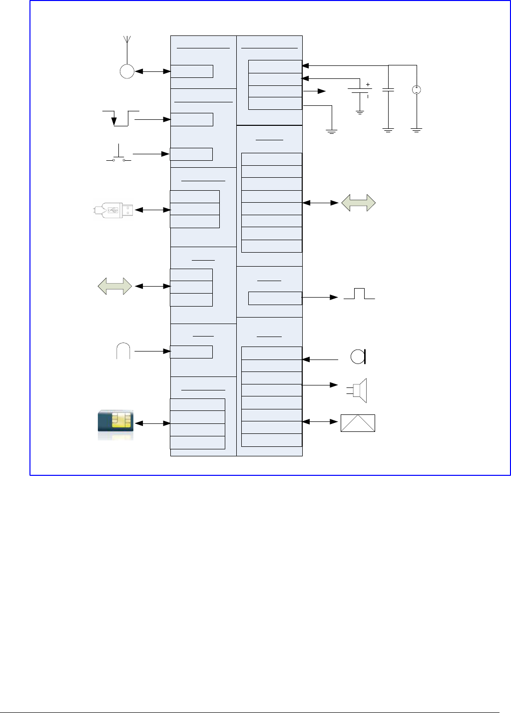
2. Block Diagram
Antenna Port
RF_Con
Power Control
PWON
RESET
Antenna
Power on
Signal
Reset
USB Slave
UART_DSR
USB_DP
USB_DN
VUSB
USB
Master
GPIO
GPIO 1
GPIO 2
GPIO 3
Three
GPIO
ADC
ADC
External
Analog
input
USB Slave
SIM 3V &
1.8V SIM_CLK
SIM_RST
SIM_DATA
VSIM
Power Supply
VBACKUP
VBAT(4)
VGPIO
GND(4) 47uF
DC 3.7V
Battery
2.85V
UART
UART_DCD
UART_TX
UART_CTS
UART_RX
UART_RTS
UART_RI
UART_DTR
Full UART
PWM
PWM
Audio
UART_DSR
MIC_N
MIC_P
HSET_P
HSET_N
PCM_IN
PCM_SYNC
PCM_OUT
PCM_CLK
HiLo3G-850
Vibrating
device
Microphone
Speaker
PCM
Figure 1: HiLo3G-850 module Block diagram
HiLo3G-850 User Manual
04 March 2011 - Page 7 / 36
3. Functional Integration
Advancements in Silicon technologies head toward functionality improvement with less power consumption. The HiLo3G-
850 module with its industrial 40 pins connector meets all these requirements, using the latest high end technology in a
very compact design of only 27 x 27 x 4.8 mm and weighs less than 7 grams.
All digital I/Os among the 40 pins are in the 2.9V domain suitable for most systems except SIM I/O's, which can also
be in the 1.8V domain depending on SIM-card use and PWON in the 1.8V domain.
Analogical I/O are in the following power domains:
• VSIM SIM I/Os in the 1.8V or 2.9V domain
• VBACKUP 3V domain
•VGPIO 2.9V domain
•VBAT from the 3.2V to the 4.4V domain. 3.7V is normal.
•VUSB 5V domain
•ADC 2.1V domain
•MIC_N/P 1.8V domain
•HSET_N/P VBAT domain
•Antenna RF power Amplifier is on VBAT domain
•Operation temperature from the -40℃ to the +85℃
Do not power on the module I/O with a voltage over the specified limits. This could damage the module.
Acoustic engineering competencies are mandatory to obtain accurate audio performance from customer products.
Radio engineering competencies are mandatory to obtain accurate radio performance from customer products.
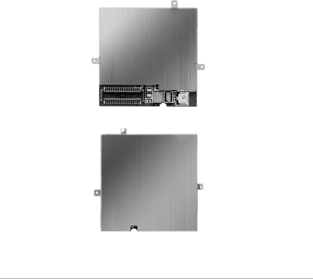
Figure 2: HiLo3G-850 module connector side
Figure 3: HiLo3G-850 module back side
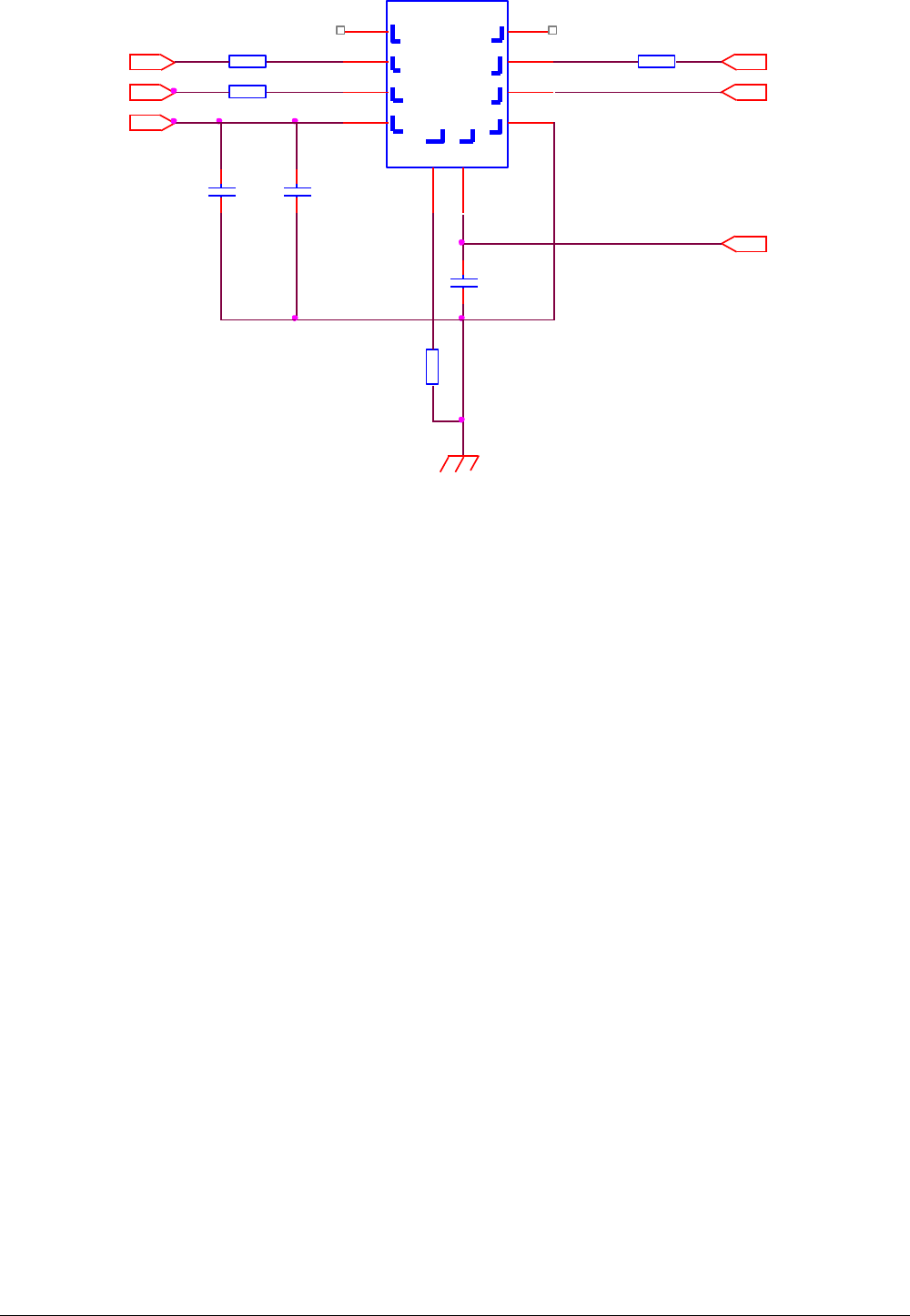
3.1. How to connect a SIM card
HiLo3G-850 User Manual
04 March 2011 - Page 8 / 36
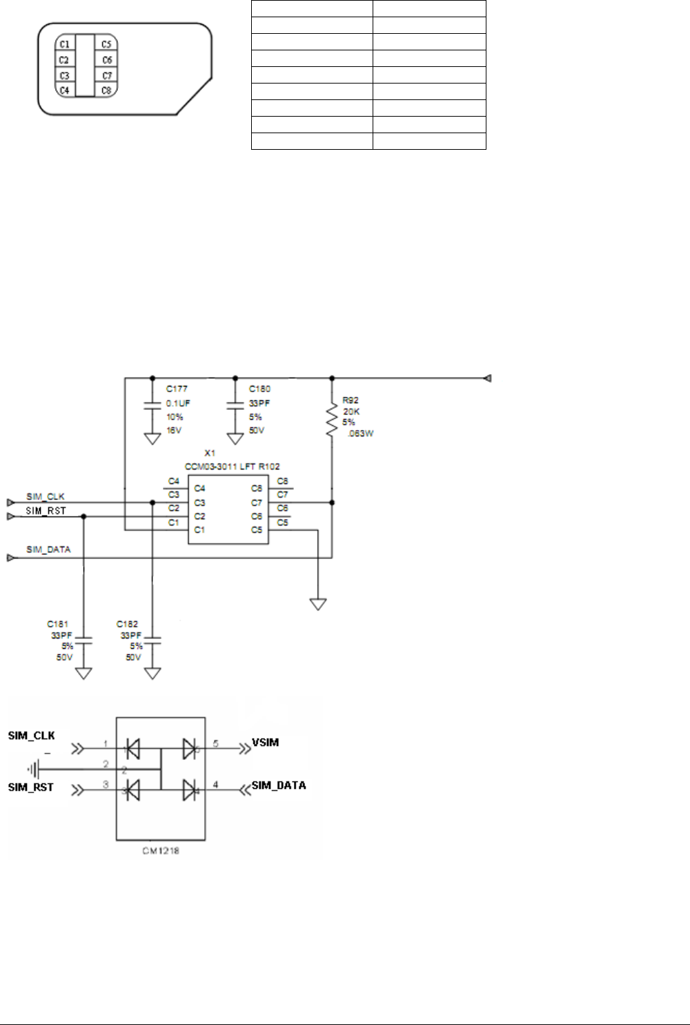
Figure 4: SIM Card signals
The HiLo3G-850 module provides SIM signals to the 40 pins. A SIM card holder with 6 pins must be adopted to use the
SIM function.
Decoupling capacitors must be added on VSIM,SIM_DATA,SIM_RST,and SIM_CLK signals as close
as possible to the SIM card connector to avoid EMC issues and pass SIM card approval tests.
Use ESD protection components to protect SIM card and module I/Os against Electro Static Discharges.
The following schematic shows how to protect SIM access of a 6 pins connector. This must be performed every time a SIM
card holder is accessed by the end user customer.
Figure 5: EMC and ESD protection components close to SIM
In cases of long SIM bus lines over 100mm, using serial resistors to avoid electrical overshoots on SIM bus signals is
recommended. Use 56 Ω for the clock line and 10Ω for the reset and data lines.
PIN No.
Name
C1
VCC
C2
RST
C3
CLK
C4
NA
C5
GND
C6
VPP
C7
I/O
C8
N/A
VSIM
HiLo3G-850 User Manual
04 March 2011 - Page 9 / 36
1
6
5
4 8
7
3
2
9
10
SIM_RST_CARD
SIM_CLK_CARD
VSIM_CARD
SIM_DATA_CARD
VSIM_CARD
SIM_GPIO
C601
10nF
C602
33pF
C60322pF
R601
R602
56
10
10
R601
NC
NC
2.2k
R616
GND
Figure 6: Serial resistors for protection of long SIM bus lines
The schematic here above includes the hardware SIM card presence detector. It can be connected to any GPIO and
managed with an AT command.
The SIM card must not be removed from its holder while it is still powered. First switch the module off properly with
the AT command, then remove the SIM card from its holder.
3.2. Connect Audio
The HiLo3G-850 module features two input audio paths and two output audio paths. The two input paths, one is
differential analog microphone and the other is PCM digital input. The two output paths, one is a differential analog 32Ω
speaker and the other is PCM digital output.
In this following chapter design examples will be given including protections against EMC and ESD and some notes about
the routing rules to follow to avoid TDMA noise sometimes present in this sensitive area of design.
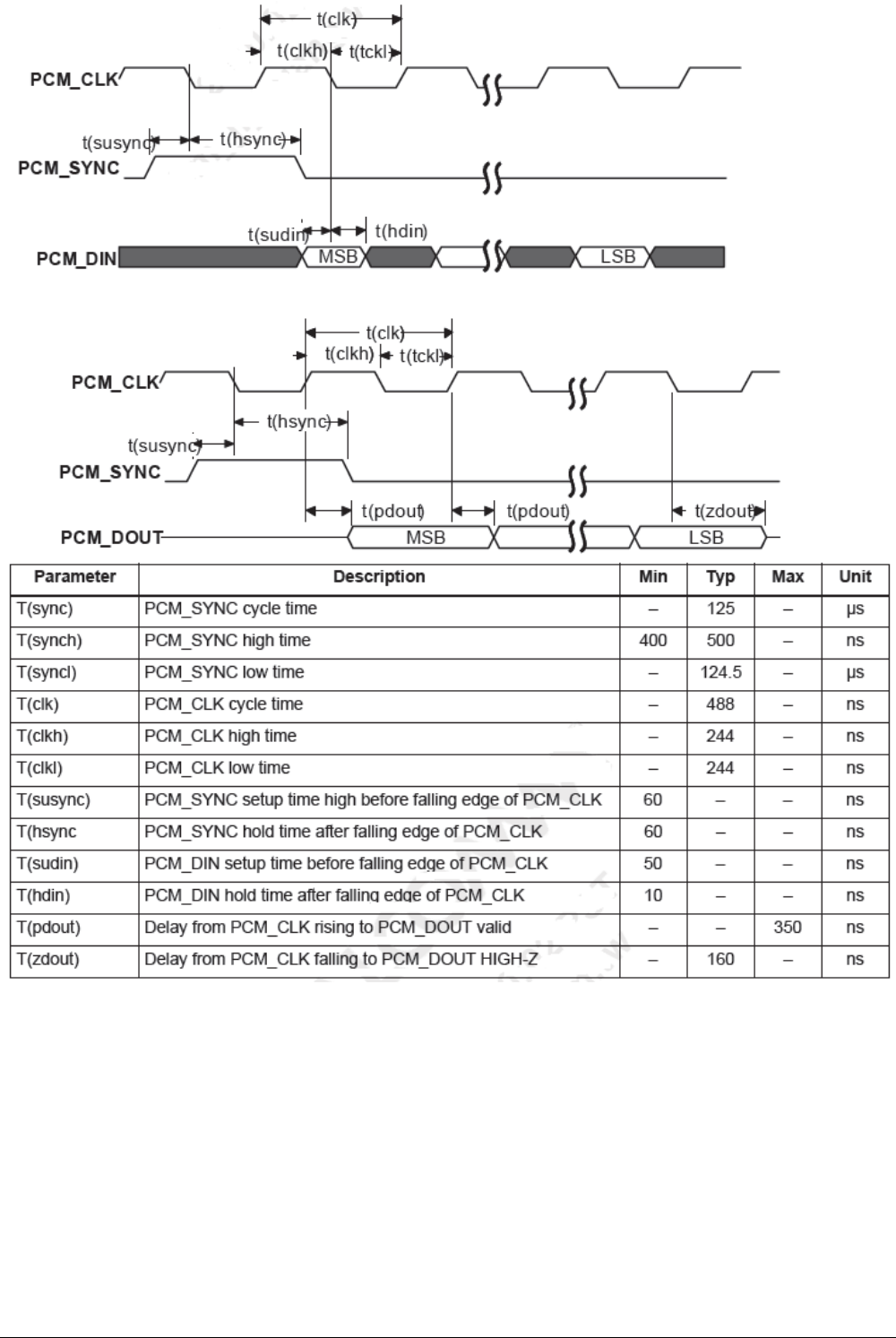
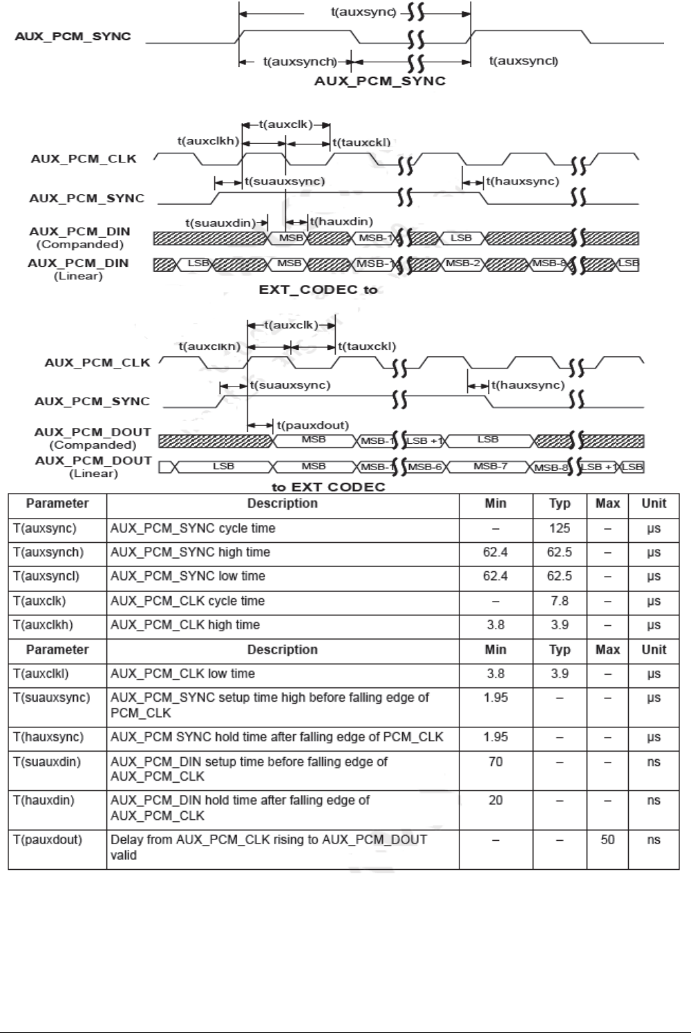
3.2.1 PCM Digital Audio
HiLo3G-850 can be used for connections to an external codec through the integrated PCM interface. The interface supports
an 8 kHz short sync mode at 2048 kHz and an 8 kHz long sync mode at 128 kHz. In the short-sync (primary PCM) mode,
the HiLo3G-850 can be a master or a slave. In the long-sync (auxiliary PCM) mode, the HiLo3G-850 is always a master;
there is no slave support.
HiLo3G-850 User Manual
04 March 2011 - Page 10 / 36
Figure 7: Primary PCM mode timing parameter
HiLo3G-850 User Manual
04 March 2011 - Page 11 / 36
Figure 8: Auxiliary PCM mode timing parameter
HiLo3G-850 User Manual
04 March 2011 - Page 12 / 36
3.2.2 Analog Audio
Analog audio is connected via MIC_N and MIC_P as input and HSET_N and HSET_P as output to the HiLo3G-850.
Please note that external circuitries are mainly needed for the microphone and speaker.
Figure 9: Analog audio connections
3.2.2.1 Microphone Note
Careful attention must be given to the microphone device design because it must not be sensitive to RF disturbances.
If you must have deport microphone out of the board using long wires, extra care must be given to avoid EMC and ESD
effects. It is also the case when your design is ESD sensitive. In those cases, add the following protections to improve your
design.
To ensure proper operation of such sensitive signals, they must be isolated from others by analog grounding on
customer board layouts.
To use an external bias voltage for the microphone, simply use a capacitor of 10μF to prevent this bias voltage from
being re-injected inside the module.
Figure 10: Filter and ESD protection for microphone
3.2.2.2 Note for Speaker
The differential analog output of the HiLo3G-850 is able to drive a 32 Ohms telephone receiver directly. In case there is
a need to drive something different, e.g. an 8 Ohms speaker, an external amplifier is required.
HSET_P, HSET__N tracks must be larger than other tracks: 0.3 mm.
Differential signals have to be routed in parallel.
To use an external audio amplifier connected to a loud-speaker, use serial capacitors of 10nF on the HiLo3G-850 audio
outputs to connect the audio amplifier.
HiLo3G
-850
ESD protection
Mic.
Speaker
MIC
33pF
33pF
Ferrite Bead
Ferrite Bead
+
ESD protection
ESD protection
HiLo3G-850
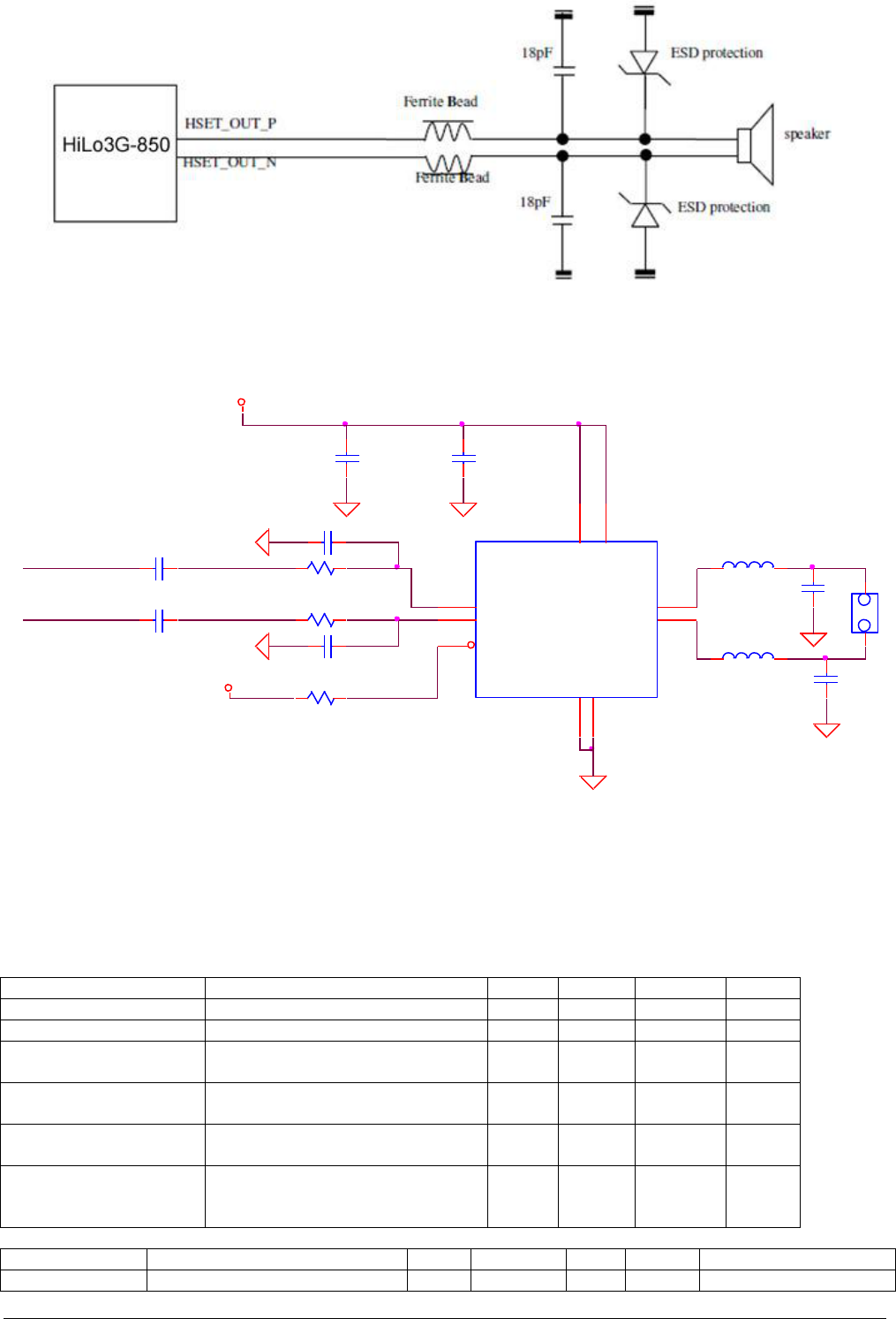
HiLo3G-850 User Manual
04 March 2011 - Page 13 / 36
Reference Bead: Murata BLM18HD102SN1D
Figure 11: Filter and ESD protection for 32 ohms speaker
SPK1
12
C77NC
R114 100KR2F
C80
NC
B2
BLM18HD102SN1D
C81
NC
VIN_3.7
VIN_3.7
C70 10uC16TAM10
SPKR_OUT+_1
C74
0.1uC2X7K16
C71 10uC16TAM10
SPKR_OUT-_1
R112 150kR2F
C72
10uC5X7K10
B3
BLM18HD102SN1D
R113 150kR2F
C73NC TPA2010D1YZFTU22
GND
B3 V_DD B1
V_O- A3
V_O+ C3
IN-
C1 IN+
A1
PV_DD B2
SHUTDOWN*
C2
GND
A2
Figure 12: Example of D class TPA2010D1 1Watt audio amplifier connections
3.2.2.3 Recommended Microphone Characteristics
Microphone: 8 and 16 kHz sampling rate, 16 bit.
In addition to the headset with microphone, the only external components required to implement this feature is one 2.2 k
resistor and two 0.1μF caps.
Parameter
Comments
Min
Typ
Max
Units
MIC bias voltage
–
1.8
–
V
MIC bias current
Programmable
0.020
–
1.50
mA
MIC bias voltage
accuracy
Minimum load
-3
–
+3
%
MIC bias voltage load
regulation
30
–
–
Ω
Load capacitor
At HSED_BIAS pin; ensures
stability
0.1
–
1.0
uF
Supply current
Active state
Idle state
–
50
10
100
100
uA
nA
Parameter
Test conditions
Min
Typ
Max
Units
Notes
Full-scale input
Voltage across either MIC1P and
0.89
1
1.12
Vrms
HiLo3G-850 User Manual
04 March 2011 - Page 14 / 36
voltage
MIC1N,
MIC2P and MIC2N, or
LINEIN_LP and
LINEIN_LN, 0 dB gain
Voltage across either MIC1P and
MIC1N,
MIC2P and MIC2N, or
LINEIN_LP and
LINEIN_LN, 24 dB gain
56.2
61.3
70.8
Vrms
Gain error
(absolute)
0 and 24 dB gain settings for all
inputs.
Measured at 13 dB below the
maximum
input level for the given gain
setting.
-1
0.2
1
dB
Output referred
noise
0 dB gain, input grounded
A-weighted
–
-86.92
-
88.91
dBFS
24 dB gain, input grounded
A-weighted
–
-83.92
-
83.92
dBFS
Input
impedance
Differential mode
16
20
24
kΩ
Single-ended mode
8
10
12
kΩ
Parameter
Test conditions
Min
Typ
Max
Units
Notes
THD+N ratio
0 dB analog gain
Input frequency = 1.02 kHz
Output = -1 dBFS
40
90.84
–
dB
Measurement BW =
22 to Fs/2; (no
A-weighting)
24 dB analog gain
Input frequency = 1.02 kHz
Output = -1 dBFS
40
82.43
–
dB
Input
capacitance
At each pin, for all inputs
–
–
5
pF
Input offset
voltage
-5
–
5
mV
Signal-to-noise
ratio
0 dB gain, input grounded
A-weighted
TBD
TBD
–
dB
24 dB gain, input grounded
A-weighted
TBD
TBD
–
dB
Sensitivity
- 39 dB
~-42 dB
SPL(0 dB
= 1 V/Pa
@ 1kHz)
Figure 13: Microphone performance requirements
3.2.2.4 Recommended Speaker Characteristics
Item to be inspected
Acceptance criterion
Input power: rated / max
0.1W (Rate)
Audio chain impedance
32 ohm +/- 10% at 1V 1KHz
Frequency Range
300 Hz ~ 4.0 KHz
Sensitivity (S.P.L)
>105 dB at 1KHz with IEC318 coupler
Distortion
5% max at 1K Hz, nominal input power
HiLo3G-850 User Manual
04 March 2011 - Page 15 / 36
Figure 14: Speaker performance requirements
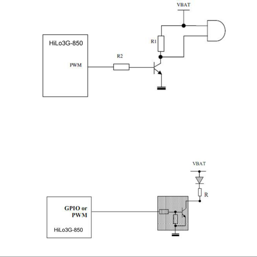
3.3 PWM
One PWM pin is available on the HiLo3G-850. It‘s a general purpose PWM which can be used for driving a vibrating
device, keypad backlight or LED. The PWM pin can be controlled through AT commands, allowing several periods and
duty cycles. More details are given in the AT commands specifications document.
User application can set PWM output:
Frequency between: 0.125Hz and 8KHz
Duty range from: 0 to 100%
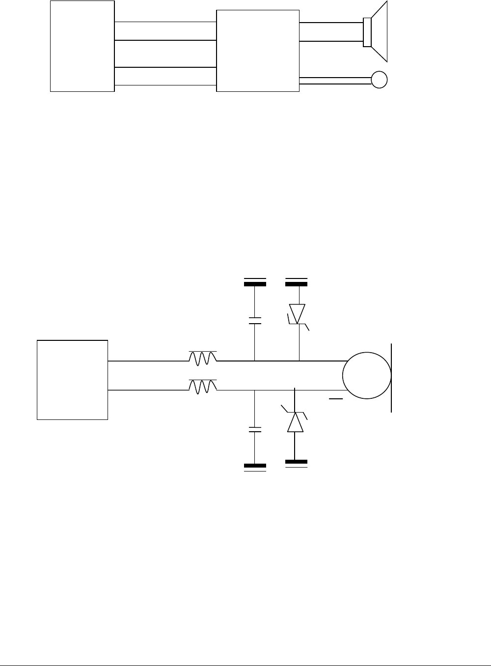
3.3.1 PWM for Buzzer connection
HiLo3G-850 module can manage PWM output to drive a buzzer. The buzzer can be used as an abnormal state alarm.
Resistors must be added to protect the buzzer. The value of these resistors depends on the buzzer and the transistor.
Normally, they can be set at 1KΩ.
Figure 15: Buzzer connection
3.3.2 Network LED
The HiLo3G-850 module can manage a network LED. The LED can be connected either to one of the available GPIO or to
the PWM.
The transistors can be found a in a single package referenced as UMDXX or PUMDXX Family.
Value of resistor R depends on characteristic of chosen LED; it is used to limit the current through the diode.
Use the AT command to set the GPIO or PWM used to control the LED.
Figure 16: Network LED connection
HiLo3G-850 User Manual
04 March 2011 - Page 16 / 36
3.4 Power Requirements
The host system must supply 3.2V ~ 4.4V to VBAT.
Within normal 2G and 3G operational modes, the maximum average current is about 1.1A depending on RF output
power. In 2G mode peak current can be as high as 2A under matched antenna condition. Peak currents could occur up to
1.75A in the case of a mismatched antenna. In the 3G mode and under antenna mismatch condition, peak current may
increase up to 700mA.
VBAT traces are required to be as short and as wide as possible. Connectors that introduce additional resistance must be
avoided whenever possible. In case it is necessary to change the PCB layer carrying the VBAT lines have several routing
options in parallel available to connect VBAT traces on different layers relative to each other.
VBAT ceramic decoupling capacitors of at least 100μF/10V are required to ensure good RF performance. Placing them
close to the connection pad of the module and connecting them with low resistance tracks to VBAT and GND is strongly
recommended.
Host power must be capable of sourcing enough current to accommodate the maximum power in cases of 2G
transmission bursts. This can be done, for example, by adding a large capacitor with a low ESR value.
PCB tracks must be well dimensioned to support 2.2A maximum current. Voltage ripple caused by serial resistance of
power supply path could result in voltage drop cases.
The HiLo3G-850 does not manage battery charging.
3.5 UART
The HiLo3G-850 has one UART port that can be used in the low-speed, full-speed, and high-speed modes. The UART
communicates with serial data ports that conform to the RS-232 interface protocol. With a properly written and user-
defined download program, the UART can be used as the serial data port for testing and debugging.
Management of external access to the V24 interface, in order to allow easy software upgrades is recommended.
Baud rate up to 4Mbps
Unused signals remain disconnected.
Signal name
Signal use (DTE point of view)
UART_DSR
Signal UART interface is ON
UART_DCD
Signal data connections in progress
UART_TX
Transmit data
UART_CTS
Signal HiLo3G-850 is ready to receive AT commands, has woken
up
UART_RX
Receive data
UART_RTS
Wakes up the module when Ksleep=1 is used
UART_RI
Signal incoming calls (voice and data), SMS, etc.
UART_DTR
Prevents the HiLo3G-850 from entering into the sleep mode
Switches between the data mode and the command modes
Wakes up the module.
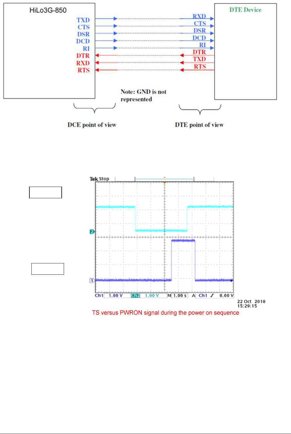
3.5.1 Complete V24—Connection HiLo3G-850 -host
A V24 interface is provided on the 40 pins of the HiLo3G-850 module with the following signals: RTS/CTS, RXD/TXD,
DSR, DTR, DCD, RI.
The use of this complete V24 connection is required whenever your application exchanges data.
HiLo3G-850 User Manual
04 March 2011 - Page 17 / 36
Figure 17: Complete V24 connection between the HiLo3G-850 and the host
This configuration allows the use flow control RTS & CTS to avoid any overflow error during data transfer. Also, CTS is
used to signal when the HiLo3G-850 is ready to receive an AT command after a power up sequence or a wake up from the
sleep mode.
Figure 18: C
In addition, this signal configuration enabled all signals :
• RI signal used when programmed to indicate an incoming voice or data call or SMS incoming message, etc.
• DCD signal used to signal the GPRS connections
• DSR signal used to signal that the module UART interface is ON
• DTR signal used to prevent the HiLo3G-850 from entering into the sleep mode, switching between Data and AT
commands, hanging up a call or waking up the module etc.
Pull-up resistors of 100KΩ to VGPIO must be connected to DCD, DSR and RI signals.
Avoid supplying the UART before the HiLo3G-850 is ON, this may result in power up sequence error.
3.5.2 Complete V24 Interface with PC
To use theV24 interface, some adaptation of components is necessary to convert the signals from the HiLo3G-850 to +/-
PWRON
CTS
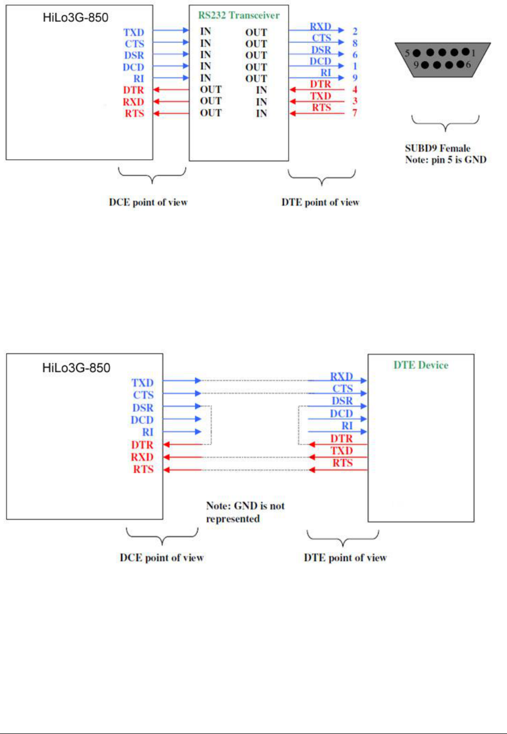
HiLo3G-850 User Manual
04 March 2011 - Page 18 / 36
5V signals compatible with a PC.
Figure 19: Connection to a data cable
Pull-up resistors of 100KΩ to VGPIO must be connected to DCD, DSR and RI signals.
Avoid supplying the UART before the HiLo3G-850 is ON, this could result in bad power up sequence. To have a proper
behavior use the signal VGPIO to enable the RS232 Transceiver.
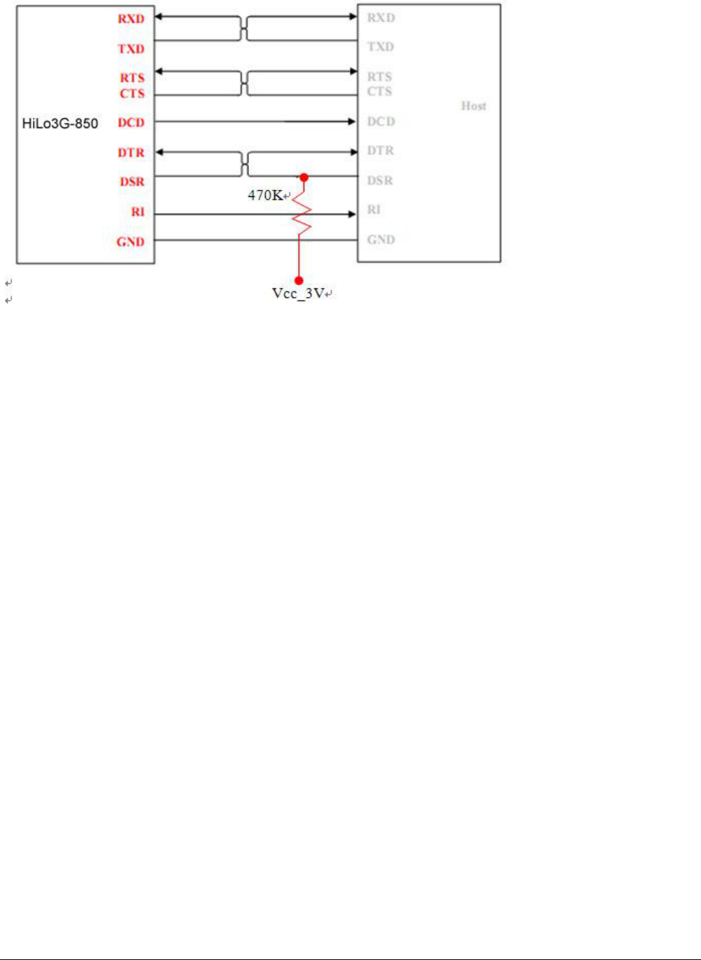
3.5.3 Partial V24 (RX-TX-RTS-CTS)—Connection HiLo3G-850 -host
When using only RX/TX/RTS/CTS instead of the complete V24 link, the following schematic could be used.
Figure 20: Partial V24 connection (4 wires) between HiLo3G-850 and host
As DSR is active (low electrical level) once HiLo3G-850 is switched on, DTR is also active (low electrical level),
therefore AT command AT+Ksleep can switch between the two sleeps mode available for HiLo3G-850.
DTR input signal is internally pull upped to VGPIO with a 100KΩ, this result in 28μA of extra consumption.
DCD and RI can stay not connected and floating when not used. Otherwise use 100KΩ pull up to VGPIO.
This configuration allows using the flow control RTS & CTS to avoid any overflow error during the data transfer, CTS is
moreover used to signal when HiLo3G-850 is ready to receive an AT command after a power up sequence or a wake up
from sleep mode.
HiLo3G-850 User Manual
04 March 2011 - Page 19 / 36
However this configuration does not allow the signaling signals like:
• RI signal used when programmed to indicate an incoming voice or data call or SMS incoming etc…
• DCD signal used to signal the DATA connections
• DSR signal used to signal the module UART interface is ON (need to pull high DSR with 470K ohm to external 3V,
shown as below)
• DTR signal used to prevent HiLo3G-850 from entering into sleep mode or to switch between Data and AT commands or
to hang up a call or to wake up the module etc…
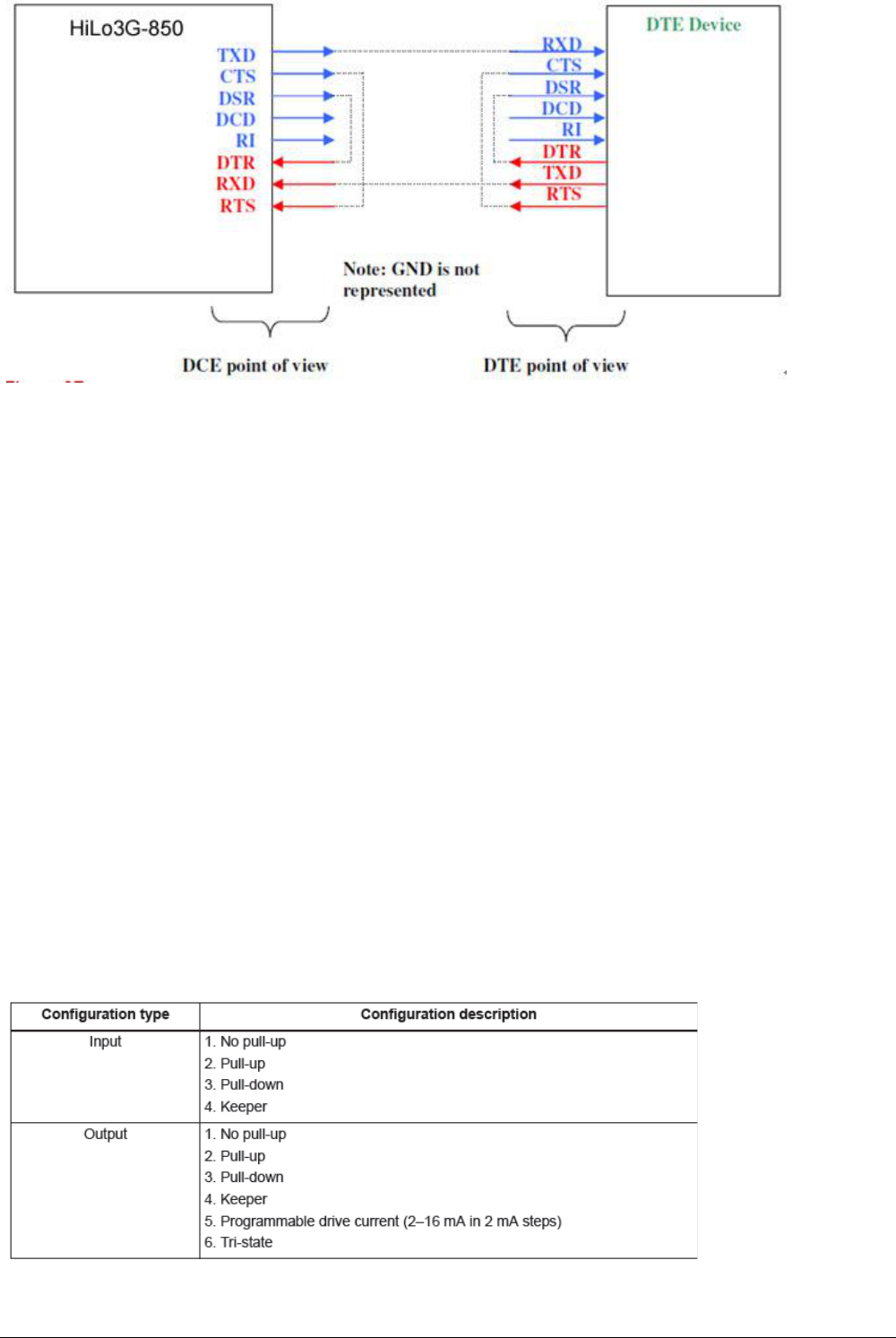
3.5.4 Partial V24 (RX-TX)—Connection HiLo3G-850 -host
When using only RX/TX instead of the complete V24 link, the following schematic could be used.
HiLo3G-850 User Manual
04 March 2011 - Page 20 / 36
Figure 21: Partial V24 connection (2 wires) between HiLo3G-850 and host
As DSR is active (low electrical level) once HiLo3G-850 is switched on, DTR is also active (low electrical level),
therefore AT command AT+Ksleep can switch between the two sleep modes available for HiLo3G-850.
DTR input signal is internally pulled up to VGPIO with a 100KΩ, this result in 28μA of extra consumption
As CTS is active (low electrical level) once HiLo3G-850 is switched on, RTS is also active (low electrical level),
therefore AT command AT+Ksleep can switch between the two sleep modes that are available for HiLo3G-850. The
HiLo3G-850's firmware allows the rise of CTS during the sleep state even when looped to RTS signal.
DCD and RI can stay disconnected and floating when not used. Otherwise use 100KΩ pull up to VGPIO.
Moreover this configuration does not allow the signaling signals as below:
• RI signal used when programmed to indicate an incoming voice or data call or SMS incoming etc…
• DCD signal used to signal the GPRS connections
• DSR signal used to signal the module UART interface is ON
• DTR signal used to prevent the HiLo3G-850 module from entering into sleep mode
3.6 GPIO
There are three GPIOs available on HiLo3G-850. Customer application can directly use them through the appropriate AT
command as:
- Output: pin is set to High or Low state
- Input: pin is read on request and answer is given to the customer application
As input, different cases are possible to cover the maximum possibility of customer application:
• Synchronous answer to the AT command
• Asynchronous answer to the AT command. The customer application prior to the request has configured the GPIO to
react on falling/rising edges. The customer application is notified asynchronously by AT command answer when the
configured trigger occurs.
Figure 22: Programmable GPIO configurations
HiLo3G-850 User Manual
04 March 2011 - Page 21 / 36
Thanks to some other special AT commands, GPIOs can for example be used:
1. Make an I/O toggling while the module is attached to the network
2. Make an I/O toggling when a programmed temperature is reached
3. As input to detect the presence of an antenna (with some external additional electronic)
4. As input to detect the SIM card presence …etc
3.7 ADC
There is one ADC input pin which can be used to read the value of the voltage applied. Following characteristics must be
fullfilled to allow proper performances:
• The input signal voltage must be within 0V and up to 2.1V
• The input impedance of the pin is 2KΩ
• The input capacitance is typically 53pF.
The AT command AT+KADC will return the voltage value with the following characteristics:
• 12 bits resolution
• Maximum sampling frequency is 2.4MHz.
3.8 Backup Battery
3.8.1 Backup Battery Function Feature
3.8.1.1 With Backup Battery
A backup battery can be connected to the module in order to supply internal RTC (Real Time Clock) when the main power
supply is removed. Thus, when the main power supply is removed, the RTC is still supplied with power and the module
keeps the time register running.
• If VBAT < 3V, internal RTC is supplied by VBACKUP.
• If VBAT ≧3V, internal RTC is supplied by VBAT.
3.8.1.2 Without Backup Battery
Without backup battery
If VBAT ≥ 1.5V, internal RTC is supplied by VBAT.
If VBAT < 1.5V, internal RTC is not supplied.
To calculate the backup battery capacity; consider that current consumption for RTC on the backup battery is up to 2µA
depending on the temperature.
Pin Name
Min
Max
VBACKUP
2uA
3.8.2 Charge by Internal HiLo3G-850 Charging Function
The charging function is available on HiLo3G-850 without any additional external power supply (the charging power
supply is provided by the HiLo3G-850).
Charge of the back-up battery occurs only when main power supply VBAT is provided.
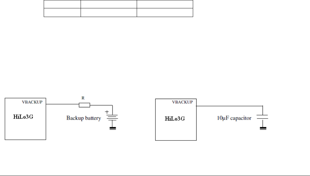
Figure 23: Backup battery or 10μF capacitor internally charged

HiLo3G-850 User Manual
04 March 2011 - Page 22 / 36
The resistor R depends on the charging current value provided by the battery manufacturer.
3.8.3 Backup Battery Technology
3.8.3.1 Capacitor Battery
These kinds of backup battery do not have the drawbacks of the Lithium Ion rechargeable battery.
As there are only capacitors:
• The maximum discharge current is generally bigger,
• There is no need to regulate the charging current.
Moreover, this kind of battery is available in the same kind of package than the Lithium Ion cell and fully compatible on a
mechanical perspective. The only disadvantage is that the capacity of this kind of battery is significantly smaller than
Manganese Silicon Lithium Ion battery. But for this kind of use (supply internal RTC when the main battery is removed),
the capacity is generally enough.
3.9 USB
There is one set USB_DP and USB_DN bi-directional differential USB data lines are compliant to the USB2.0
specification.
HiLo3G-850 is USB-Slave while customer application is USB-Master.
• Integrated high-speed USB PHY
• USB 2.0 specification-compliant as a peripheral
•The USB 2.0 specification requires hosts such as PCs to support all three USB speeds, namely low-speed (1.5 Mbps), full-
speed (12 Mbps) and high-speed (480 Mbps). The USB 2.0 specification allows peripherals to support any one or more of
these speeds.
• USB selective suspend and remote wake-up
The USB_DP and USB_DN signals are routed as a ~90 Ω differential pair. These signals must be routed side by side
and on the same layer and their trace length should match as close as possible.
2 pF capacitor is required to be installed between USB_DP and USB_DN and put close to the HiLo3G-850.
These signals have relatively fast edges, so they should be routed away from sensitive circuits and signals such as the
19.2 MHz TCXO, sleep XTAL, and RF. Therefore, do not route these signals on surface layers, it is preferred to be routed
in the inner layer routing sandwiched between power and ground.
4. Power Management
The host system shall supply 3.2V~4.4V to VBAT for powering the baseband, logics circuit and RF circuit.
4.1 Power Modes
Depending on the state of the HiLo3G-850, different power consumption modes can be identified.
Active mode (Active communication)
All systems on HiLo3G-850 are active. In this mode, the module is registered to the network and a voice/data call is
actively transmitting data.
Sleep mode (Active idle)
All systems on HiLo3G-850 are active including the USB bus. In this mode, the module is registered to the network but it
is idle/paging only. No voice/data call connection is established.
Fly mode
The processor is still active but the radio section is powered down. This mode can be controlled by sending an AT
command to the module.
HiLo3G-850 User Manual
04 March 2011 - Page 23 / 36
4.2 Module Power up
There are two ways to start HiLo3G-850, one is using PWON and the other is using USB.
4.2.1 PWON Power up
To start the module, first power up VBAT, which must be in the range 3.2V ~ 4.4V, and able to provide 1.75A during the
TX bursts.
PWON is a low level active signal internally pulled up to a dedicated power domain to 2.9V.
As PWON is internally pulled up, a simple open collector or open drain transistor can be used for ignition.
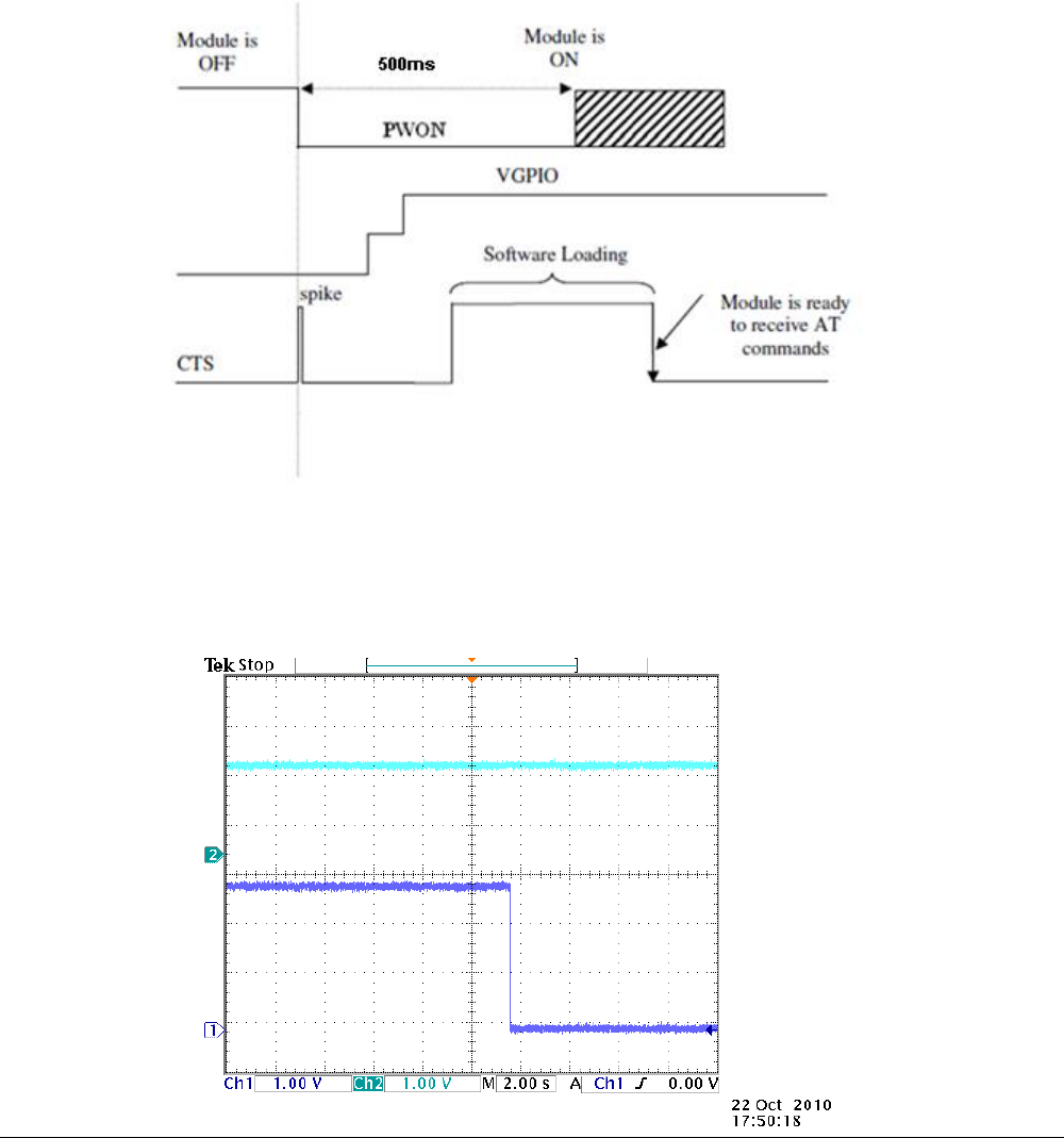
To start the module, a low level pulse must be applied on PWON during 500ms.
After a few seconds, the CTS goes to the active state when the module is ready to receive AT commands.
VGPIO is a supply output from the module that can be used to check if the module is alive.
• When VGPIO = 0V the module is OFF
• When VGPIO = 2.9V the module is ON
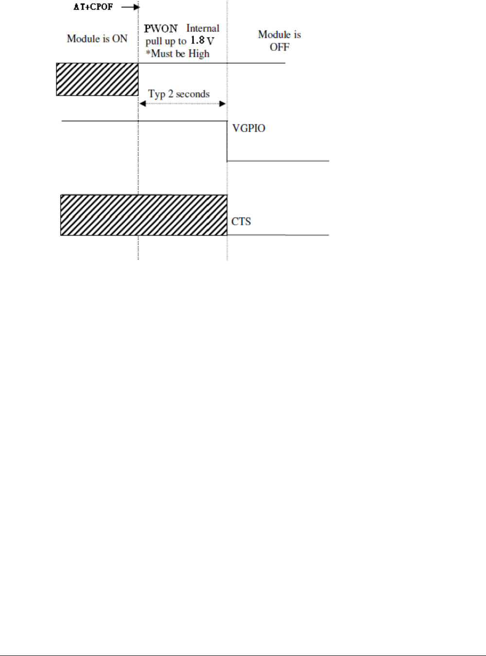
Figure 24: Power on sequence
AT+CPOF
CTS
Module Off

HiLo3G-850 User Manual
04 March 2011 - Page 24 / 36
Figure 25: Power off sequence
Send AT COMMAND ―AT+CPOF ― to power off module.
4.2.1.1 IO DC Presence before Power on
When the VBAT is available but the module not yet started, the following I/O's raised their output.
VBACKUP raise to 3V
PWON raise to 1.8V
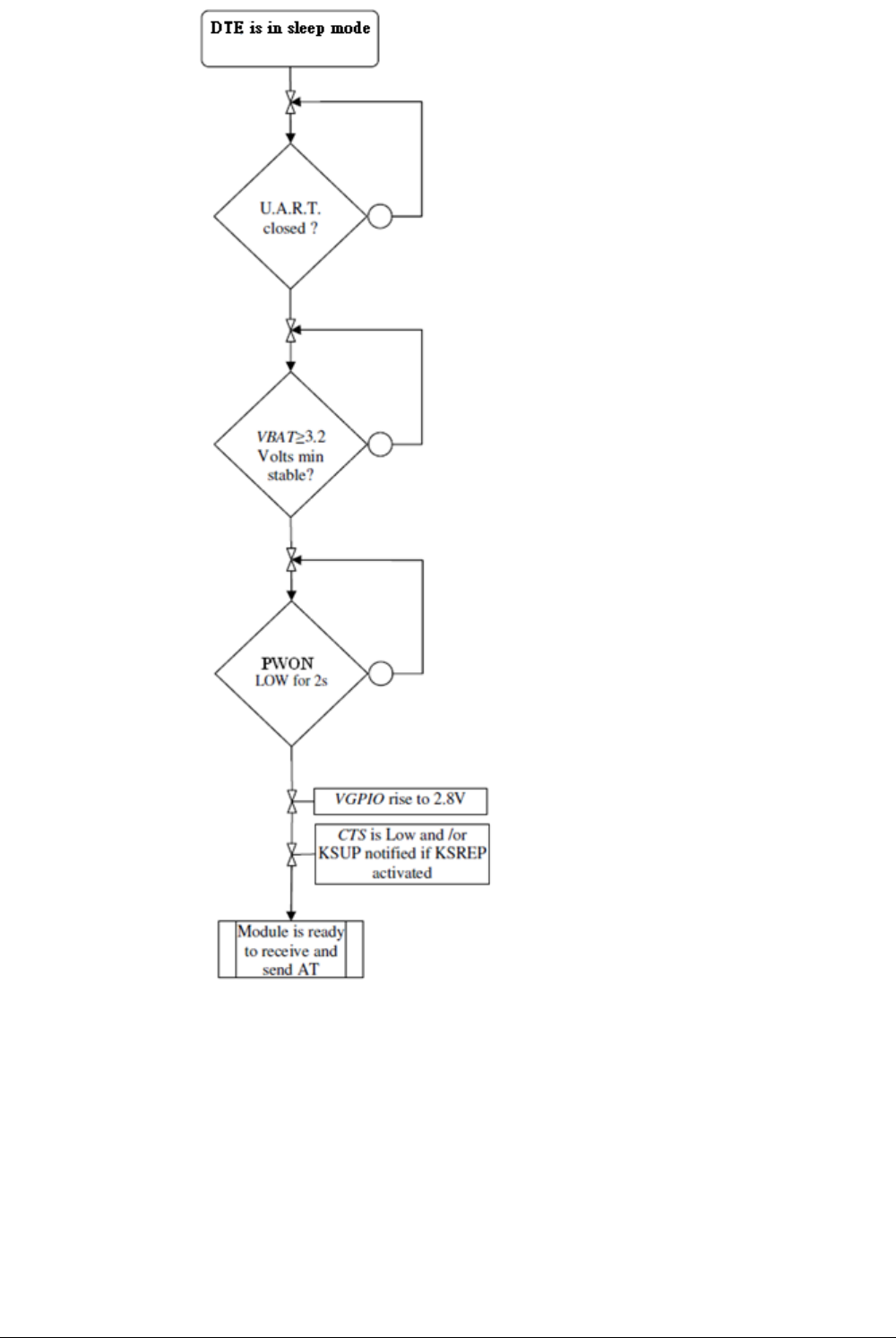
4.3 Power on and Sleep Diagrams
Those 2 diagrams show the behaviors of the module and the DTE during the power on and then in the sleep modes.
Note: The module cannot enter sleep mode if USB bus is connected.
HiLo3G-850 User Manual
04 March 2011 - Page 25 / 36
Figure 26: Diagram for the power on
HiLo3G-850 User Manual
04 March 2011 - Page 26 / 36
Figure 27: Diagram for the sleep mode
4.4 Module Power off
HiLo3G-850 User Manual
04 March 2011 - Page 27 / 36
4.4.1 UART Interface
To stop the module, use the AT command AT+CPOF. If the PWON is not pulled down the module will switch to OFF
mode after the AT command, otherwise the module restarts immediately (an OFF sequence is performed followed by a
power ON sequence).
Figure 28: Power off sequence for PWON, VGPIO and CTS
4.4.2 USB Interface
As the module can also start when an USB cable is plugged, the sequence to stop the module needs the USB interface to be
OFF or VBUS disconnected just after the command is sent and acknowledged by the module. Thus, to stop the module
when the USB interface is being used, use the AT command AT+CPOF, then disconnect VBUS (unplug the USB cable or
use a commanded switch to switch off VBUS) signal when the module acknowledges (responds OK) the command,
otherwise the module restarts immediately (an OFF sequence is performed followed by a power ON sequence).
4.5 Sleep Mode
The AT command ―AT+KSLEEP‖ allows configuring the sleep mode.
When AT+KSLEEP=1 has been configured:
• The HiLo module decides by itself when it enters in sleep mode (no more task running).
• ―0x00‖ character on serial link wakes up the HiLo3G-850 module.
When AT+KSLEEP=0 has been configured:
• The HiLo3G-850 module is active when DTR signal is active (low electrical level).
• When DTR is deactivated (high electrical level), the HiLo3G-850 module enters in sleep mode after a while.
• On DTR activation (low electrical level), the HiLo3G-850 module wakes up.
When AT+KSLEEP=2 has been configured:
• The HiLo3G-850 module will never enter sleep mode.
In sleep mode the module reduces its power consumption and remains waiting for the wake up signals either from the
network, from the operating system or from the host controller.
Note: The module cannot enter sleep mode if USB bus is connected.
5. ESD & EMC Recommendation
Using human body model from JEDEC JESD 22-A114 standard, HiLo3G-850 can hold 2KV on each of the 40 pins and
HiLo3G-850 User Manual
04 March 2011 - Page 28 / 36
contact areas such as antenna pads and connector.
5.1 Handling HiLo3G-850
HiLo3G-850 are packaged in boxes.
HiLo3G-850 contains electronic circuits sensitive to human hand's electrostatic electricity.
Handling without ESD protection could result in permanent damages or even destruction of the module.
5.2 ESD Recommendations
ESD current can penetrate into the device via the typical following components:
• SIM connector
• Microphone
• Speaker
• Battery / data connector
• All pieces with conductive paint.
In order to avoid ESD issues, efforts shall be done to decrease the level of ESD current on electronic components
located inside of the device (customer‘s board, input of the HiLo3G-850, etc…)
5.2.1 Avoid ESD
Ensure good ground connections of the HiLo3G-850 to the customer‘s board.
Flex (if any) shall be shielded and FPC connectors shall be correctly grounded at each extremity.
Put capacitor 100nF on battery, or better put varistor or ESD diode in parallel on battery and charger wires (if any) and
on all power wires connected to the module.
Uncouple microphone and speaker by putting capacitor or varistor in parallel of each wire of these devices.
Here are the pin number to be protected over 2KV and references of varistors.
Pin1/2/39/40: VBAT
Pin5/6/7: USB
Pin10: VGPIO
Pin15/16/24/25: USIM
Pin19/20: Microphone
Pin21/22: SPK
Part
Vendor
Part number
Varistor
LITTLEFUSE
V0402MHS12NR
Varistor (for USB line)
COOPER
0402ESDA-MLP1
5.3 EMC recommendations
In case of EMC issue due to a headset audio device, the solution may consist in inserting a filter on the wires of the
microphone and of the speaker.
6. Radio Integration
HiLo3G-850 incorporates the technology for RF transceiver that converts received signals directly from RF-to-baseband
and transmits signals directly from baseband-to-RF (known as direct conversion or zero intermediate frequency (ZIF)
processing). This technique eliminates the need for large IF surface acoustic wave (SAW) filters and supporting IF and LO
HiLo3G-850 User Manual
04 March 2011 - Page 29 / 36
circuits.
6.1 Antenna Connection
HiLo3G-850 provides two methods to connect an antenna, one is spring contact and the other is UFL RF connector.
Definition of the reference antenna connector:
• Strictly 50 Ohms matched impedance PCB tracks
• Straight PCB tracks
Antenna gain:
• Radiation pattern: depending on antenna position and size of the device
• Gain averaged in space in all frequencies: > -3dBi
• Maximum VSWR: < 1.5:1 with 50 Ohms reference impedance
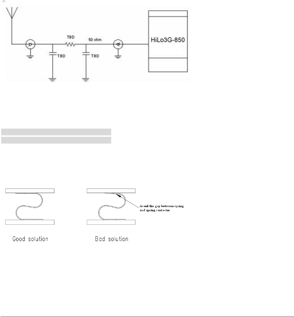
In order to get the best sensitivity and output power, it is recommended to implement a matching circuit between the
module and the antenna:
Figure 29: Antenna connection reference
6.1.1 Antenna Connector
A 50-Ohm RF connector on the HiLo3G-850 PCB is available for antenna (RF cable) connection.
Reference
HIROSE U.FL-R-SMT-1 (10)
6.1.2 Spring Contact
50 Ω line matching
Recommends to solder the spring contact on the whole surface instead of only 2 points
Figure 30: Spring contact
6.1.3 Antenna Notice
Antenna for HiLo3G-850 should be resonated in the operating bands (GSM 850, 900, 1800, 1900 + UMTS band 1, 2, 5)
depending on HiLo3G-850 reference.
Pay attention to the RF-impedance of the HiLo3G-850 (50Ω)
HiLo3G-850 User Manual
04 March 2011 - Page 30 / 36
Use low loss antenna cable (max. 0.5dB).
To avoid interference choose an antenna type radiating off the device.
Circular polarized antennas are preferred.
Verify the operation of the antenna by measurement of the total radiated power.
Avoid placing a transmit antenna close to sensitive areas (danger from interference).
Apply EMC-design rules and follow shielding concepts.
Separate of EMC-sensitive and high-emission areas.
6.2 Ground Link Area
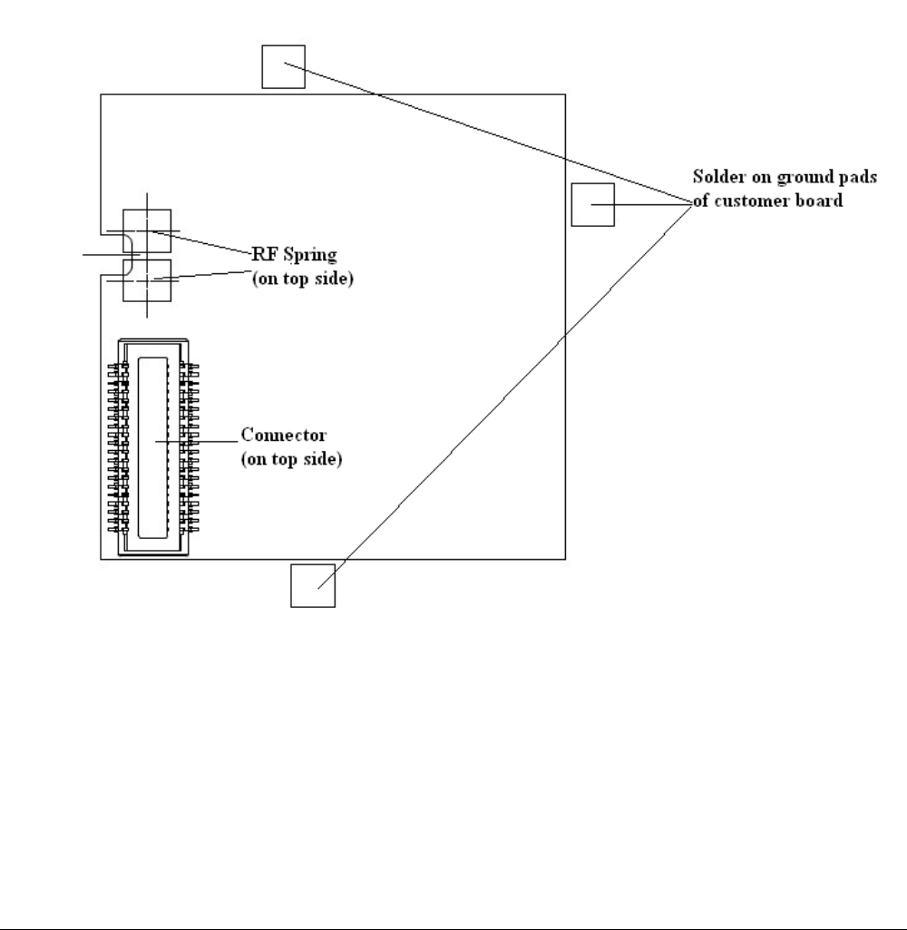
Good ground GND contact between the module and customer‘s board is required to have the best radio performances
(spurious, sensitivity…)
All HiLo3G-850 GND pins must be connected to the GND of the customer‘s board.
Solder the three pads of the shielding on the ground pads of customer board, then the HiLo3G-850 will have a good
ground contact with the customer board.
Figure 31: Ground HiLo3G-850 to customer board
6.3 Layout
Isolate RF line and antenna from other bus or signals
No signals on 50 ohms area and if that is not possible, add ground shielding using different layers.
Do not add any ground layer under the antenna contact area.

HiLo3G-850 User Manual
04 March 2011 - Page 31 / 36
Do not add signal unvarnished layout trace on the first layer of the customer board, or unvarnished via holes under the
module shield area or it will result on short circuit on those signals. This is mandatory.
Free CAD software can be used to compute the stack-up parameters that leads to a compliant 50Ω RF track.
6.4 Mechanical Surrounding
Do not apply mechanical pressure over the HiLo3G-850 shield, doing so could damage the mechanical structure of the
shield and lead to internal short-circuits or other undesirable issues.
Avoid letting any metallic part be around the antenna area
Keep FPCs and battery contact (if any) away from antenna area.
FPC's (if any) have to be shielded
6.5 Other Recommendation—test for production/design
SagemCom guarantees the RF performances in conductive mode but strongly recommends making RF measurements in an
anechoic chamber in radiated mode (tests conditions for FTA): the radiated performances strongly depend on radio
integration (layout, antenna, matching circuit, ground area…..)
7. Audio Integration
Audio mandatory tests for FTA are done in handset mode only so a particular care must be taken to the design of audio
(mechanical integration, gasket, electronic) in this mode.
The audio norms which describe the audio tests are 3GPP TS 26.131 & 3GPP TS 26.132.
7.1 Mechanical integration and acoustics
Particular care to Handset Mode:
To get a better audio output design (speaker part) :
The speaker must be completely sealed on the front side.
The front aperture must be compliant with speaker supplier‘s specifications
The back volume must be completely sealed.
The sealed back volume must be compliant with speaker supplier‘s specifications
Take care of the design of the speaker gasket (elastomer).
Foresee a stable and large enough area for the gasket of the artificial ear.
To get a better audio input design (microphone part) :
Take care of the design of the microphone (elastomer).
All receivers must be completely sealed on the front side.
Microphone sensitivity depends on the shape of the device eg. about –40 ±3 dBV/Pa.
Promote the use of pre-amplified microphone. If needed, use a pre-amplification stage.
As audio input and output are strongly linked:
Place the microphone and the speaker as far as possible from one another.
7.2 Electronics and layout
Avoid Distortion & Burst noise
Audio signals must be symmetric (same components on each path).
Differential signals must be routed parallel.
Audio layer must be surrounded by 2 ground layers.
The link from one component to the ground must be as short as possible.
If possible separate the PCB of the microphone and the one of the speaker.
Reduce as many as possible the number of electronics components (loss of quality, more dispersion).

HiLo3G-850 User Manual
04 March 2011 - Page 32 / 36
Audio tracks must be larger than 0.5 mm.
8. Recommendations on layout of customer’s board
8.1 General recommendations on layout
There are many different types of signals in the module which are disturbing each other. Particularly, Audio signals are
very sensitive to external signals as VBAT... Therefore it is very important to respect some rules to avoid disruptions or
abnormal behavior.
Magnetic field generated by VBAT tracks may disturb the speaker, causing audio burst noise. In this case, modify
layout of the VBAT tracks to reduce the phenomena.
8.1.1. Ground
A ground plane as complete as possible
Ground of components has to be connected to the ground layer through many vias not regularly distributed.
Top and bottom layer shall have as much as possible of ground planes. Flood the empty remain surface of the layout of
those two layers with a ground plane connected to main ground with as much vias as possible.
8.1.1.1 Ground layout guidelines
Proper grounding is crucial to end-product performance. At least one layer must be a dedicated ground plane. This
ground plane is the common point referenced by all end-product circuits.
In addition to the dedicated ground plane layer, any unused space on all PCB layers should be filled with ground to
provide the most robust grounding from layer to layer.
Bypass capacitors should be connected directly to their surface layer ground fill. Multiple vias should connect each
capacitor directly to the main ground plane, with one via in the capacitor‘s pad plus several vias within the surface layer
ground fill area.
8.1.1.2 Digital ground
Digital ground should via directly to the main ground plane. In addition, each layer between layers 1 and main ground
should include ground fills directly below the center grid area‘s digital pins, with each stack of vias connecting to each
ground fill area. The large mass of copper tied together using this technique provides the best possible electrical ground and
thermal conductivity.
8.1.1.3 Analog/RF ground
The analog/RF ground pins are connected together with one another, but isolated from the digital ground (until main
ground). Like the digital pins, the analog/RF pins should via directly to the main ground plane. In addition, each layer
between layers 1 and main ground should include ground fills directly below the outer layer‘s analog/RF pins, with each
stack of vias connecting to each ground fill area. The large mass of copper tied together using this technique provides the
best possible electrical ground and thermal conductivity.
8.1.2 Power supplies
Layer for power supply signals (VBAT, VGPIO) is recommended.
Any loop of power signals layout must be avoided on the design.
Suitable power supply (VBAT, VGPIO) track width and thickness.
8.1.3 Clocks
Clock signals must be shielded between two grounds layer and bordered with ground vias.
8.1.4 Data bus and other signals
HiLo3G-850 User Manual
04 March 2011 - Page 33 / 36
Data bus and commands have to be routed on the same layer, none of the lines of the bus shall be parallel to other lines
Lines crossing shall be perpendicular
Suitable other signals track width, thickness.
Data bus must be protected by upper and lower ground plans
8.1.5 Radio
Provide a 50 Ohm micro strip line for antenna connection
8.1.6 Audio
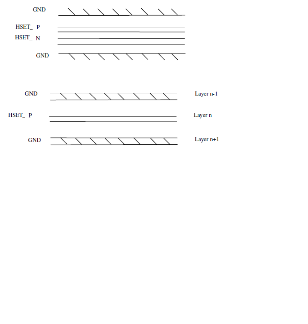
Differential signals have to be routed together, parallel (for example HSET_P/HSET_N).
Audio signals have to be isolated, by pair, from all the other signals (ground all around each pair).
Cancel any loops between VBAT and GND next to the speaker to avoid the TDMA burst noise in the speaker during a
communication.
Figure 32: Layout of audio differential signals on a layer n
Figure 33: Adjacent layers of audio differential signals
8.1.7 Shielding
A few shielding comments are provided for designer consideration:
At least the following devices and circuits should be shielded:
• High-speed memory
• RF front-end components
• Crystal circuits
• DC/DC circuits
• RF circuitry
Recommended shield partitioning:
• RF matching components, do not locate matching inductors too close to shield walls (this may cause electromagnetic
coupling and inductor de-Q).
• Memory devices must be shielded.
• The crystal circuits (other than the reference for RF frequency synthesizers) must be very close to their corresponding
pins.
HiLo3G-850 User Manual
04 March 2011 - Page 34 / 36
• Metalized plastic is not as effective as metal cans.
• Shielded inductors might be needed in the DC/DC circuits, or they might need to be placed in their own shield area.
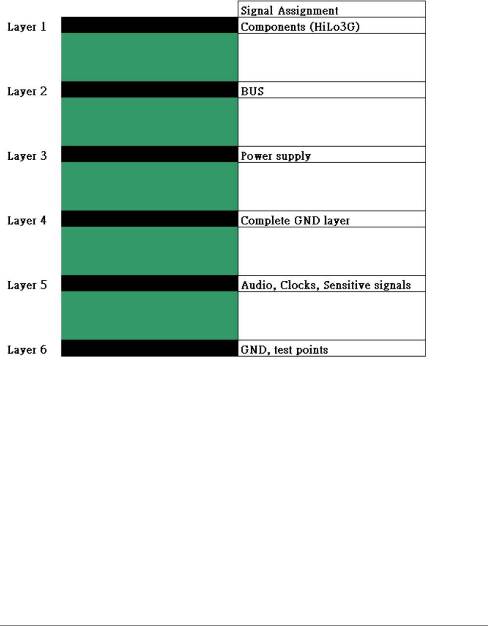
8.2 Example of layout for customer’s board
The following figure shows an example of layer allocation for a 6- layers circuit (for reference only):
Depending on the customer‘s design the layout could also be done using 4 layers.
Figure 34: Reference 6 layers PCB stack
9. Label
The HiLo3G-850 is labeled with its own FCC ID (VW3HILO3G850) on its shield side. When the module is installed in
customer‘s product, the FCC ID label on the module will not be visible. To avoid this case, an exterior label must be stuck
on the surface of customer‘s product signally to indicate the FCC ID of the enclosed module. This label can use wording
such as the following: ―Contains Transmitter module FCC ID: VW3HILO3G850‖ or ―Contains FCC ID:
VW3HILO3G850‖.
10. FCC/IC warning statement
10.1 FCC Regulations:

HiLo3G-850 User Manual
04 March 2011 - Page 35 / 36
This device complies with part 15 of the FCC Rules. Operation is subject to the following two conditions: (1) This
device may not cause harmful interference, and (2) this device must accept any interference received, including
interference that may cause undesired operation.
This device has been tested and found to comply with the limits for a Class B digital device, pursuant to Part 15 of
the FCC Rules. These limits are designed to provide reasonable protection against harmful interference in a residential
installation. This equipment generates, uses and can radiated radio frequency energy and, if not installed and used in
accordance with the instructions, may cause harmful interference to radio communications. However, there is no
guarantee that interference will not occur in a particular installation If this equipment does cause harmful interference
to radio or television reception, which can be determined by turning the equipment off and on, the user is encouraged
to try to correct the interference by one or more of the following measures:
-Reorient or relocate the receiving antenna.
-Increase the separation between the equipment and receiver.
-Connect the equipment into an outlet on a circuit different from that to which the receiver is connected.
-Consult the dealer or an experienced radio/TV technician for help.
Changes or modifications not expressly approved by the party responsible for compliance could void the user‗s
authority to operate the equipment.
10.2 RF Exposure Information
This Modular Approval is limited to OEM installation for mobile and fixed applications only. The antenna installation
and operating configurations of this transmitter, including any applicable source-based time-averaging duty factor,
antenna gain and cable loss must satisfy MPE categorical Exclusion Requirements of §2.1091.
The antenna(s) used for this transmitter must be installed to provide a separation distance of at least 20 cm from all
persons, must not be collocated or operating in conjunction with any other antenna or transmitter, except in accordance
with FCC multi-transmitter product procedures.
The end user has no manual instructions to remove or install the device and a separate approval is required for all other
operating configurations, including portable configurations with respect to 2.1093 and different antenna configurations.
Maximum antenna gain allowed for use with this device is 0 dBi.
When the module is installed in the host device, the FCC ID label must be visible through a window on the final device
or it must be visible when an access panel, door or cover is easily re-moved. If not, a second label must be placed on
the outside of the final device that contains the following text: ―Contains FCC ID: VW3HILO3G850‖.
10.3 IC Regulations:
IMPORTANT NOTE:
IC Radiation Exposure Statement:
This equipment complies with IC RSS-102 radiation exposure limits set forth for an uncontrolled
environment. This equipment should be installed and operated with minimum distance 20cm between the radiator &
your body.
This device and its antenna(s) must not be co-located or operating in conjunction with any other antenna or transmitter.
This Class B digital apparatus complies with Canadian ICES-003.
Cet appareil numérique de la classe B est conforme à la norme NMB-003 du Canada.
Under Industry Canada regulations, this radio transmitter may only operate using an antenna of a type and maximum
(or lesser) gain approved for the transmitter by Industry Canada. To reduce potential radio interference to other users,
the antenna type and its gain should be so chosen that the equivalent isotropically radiated power (e.i.r.p) is not more
than necessary for successful communication.
Conformément à la réglementation d'Industrie Canada, le présent émetteur radio peut fonctionner avec une antenne d'un
type et d'un gain maximal (ou inférieur) approuvé pour l'émetteur par Industrie Canada. Dans le but de réduire les

HiLo3G-850 User Manual
04 March 2011 - Page 36 / 36
risques de brouillage radioélectrique à l'intention des autres utilisateurs, il faut choisir le type d'antenne et son gain de
sorte que la puissance isotrope rayonnée équivalente (p.i.r.e.) ne dépasse pas l'intensité nécessaire à l'établissement
d'une communication satisfaisante.
Labeling Requirements for the Host Device (from Section 3.2.1, RSS-Gen, Issue 3, December 2010):The host device
shall be properly labeled to identify the module within the host device.The Industry Canada certification label of a
module shall be clearly visible at all times when installed in the host device, otherwise the host device must be labeled
to display the Industry Canada certification number of the module, preceded by the words ―Contains transmitter
module‖, or the word ―Contains‖, or similar wording expressing the same meaning, as follows: Contains transmitter
module IC: 9140A-HILO3G850
This device complies with Industry Canada license-exempt RSS standard(s). Operation is subject to the following two
conditions: (1) this device may not cause interference, and (2) this device must accept any interference, including
interference that may cause undesired operation of the device.Le présent appareil est conforme aux CNR d'Industrie
Canada applicables aux appareils radio exempts de licence.
L'exploitation est autorisée aux deux conditions suivantes: (1) l'appareil ne doit pas produire de brouillage, et (2)
l'utilisateur de l'appareil doit accepter tout brouillage radioélectrique subi, même si le brouillage est susceptible d'en
This radio transmitter (identify the device by certification number, or model number if Category II) has been approved
by Industry Canada to operate with the antenna types listed below with the maximum permissible gain and required
antenna impedance for each antenna type indicated. Antenna types not included in this list, having a gain greater than
the maximum gain indicated for that type, are strictly prohibited for use with this device.
Conformément à la réglementation d'Industrie Canada, le présent émetteur radio peut fonctionner avec une antenne d'un
type et d'un gain maximal (ou inférieur) approuvé pour l'émetteur par Industrie Canada. Dans le but de réduire les
risques de brouillage radioélectrique à l'intention des autres utilisateurs, il faut choisir le type d'antenne et son gain de
sorte que la puissance isotrope rayonnée équivalente (p.i.r.e.) ne dépasse pas l'intensité nécessaire à l'établissement
d'une communication satisfaisante.