SAGEMCOM BROANDS HILOC GSM/GPRS Module User Manual
SAGEMCOM SAS GSM/GPRS Module Users Manual
UserManual.wiki
>
SAGEMCOM BROANDS
>
HILOC User Manual
Users Manual
Navigation menu
Upload a User Manual
Namespaces
Wiki Guide
HTML
PDF
Info
Views
User Manual
Discussion / Help
Navigation
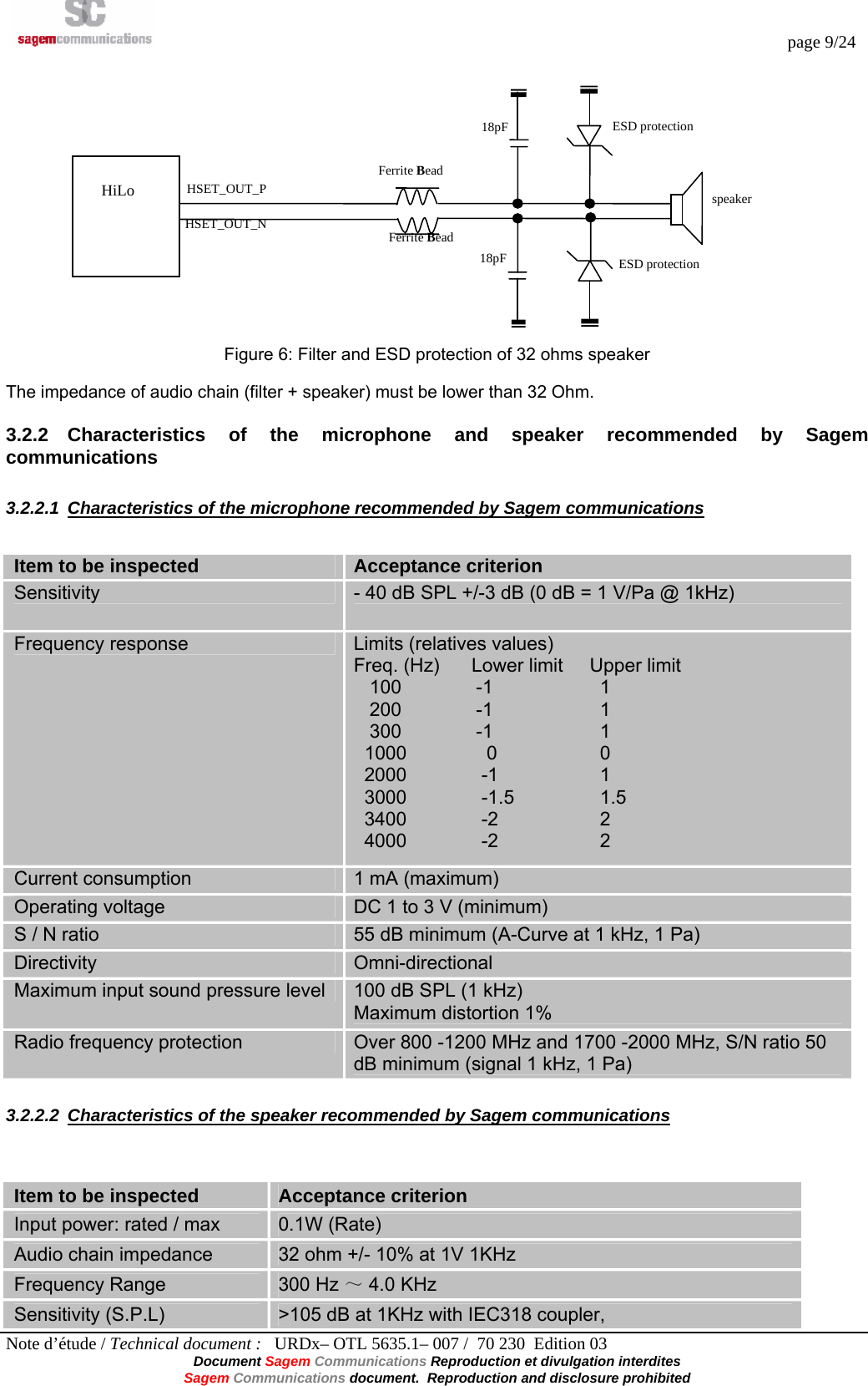
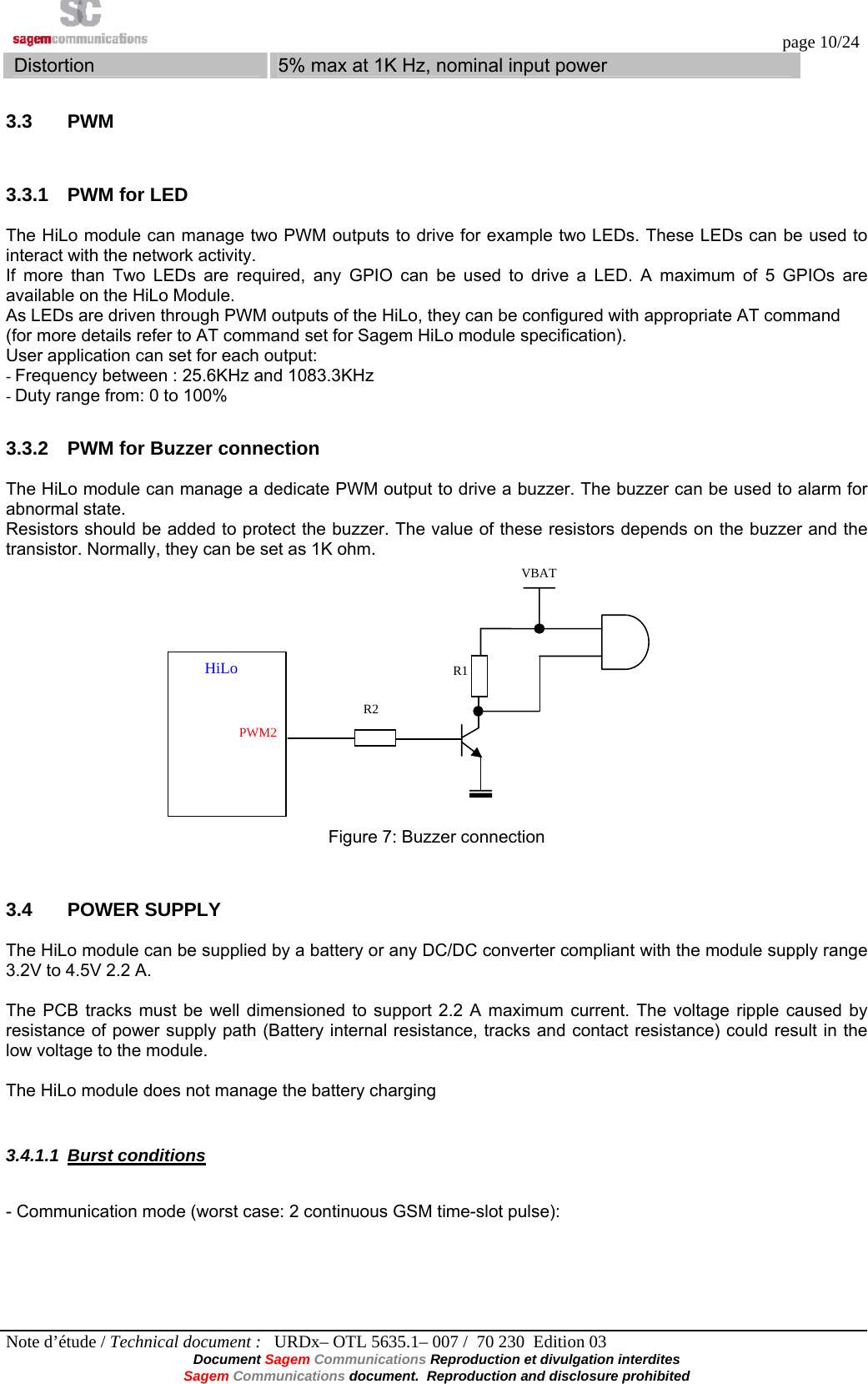
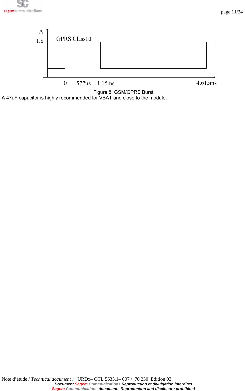
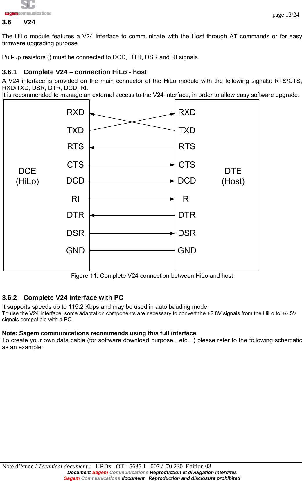
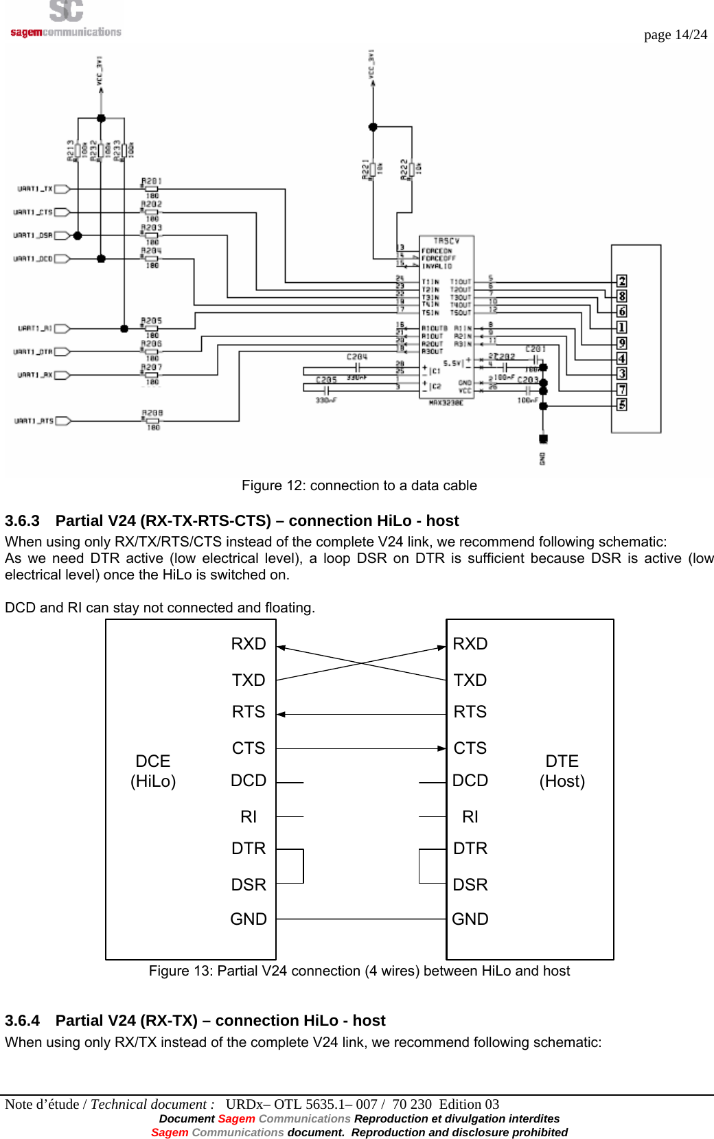
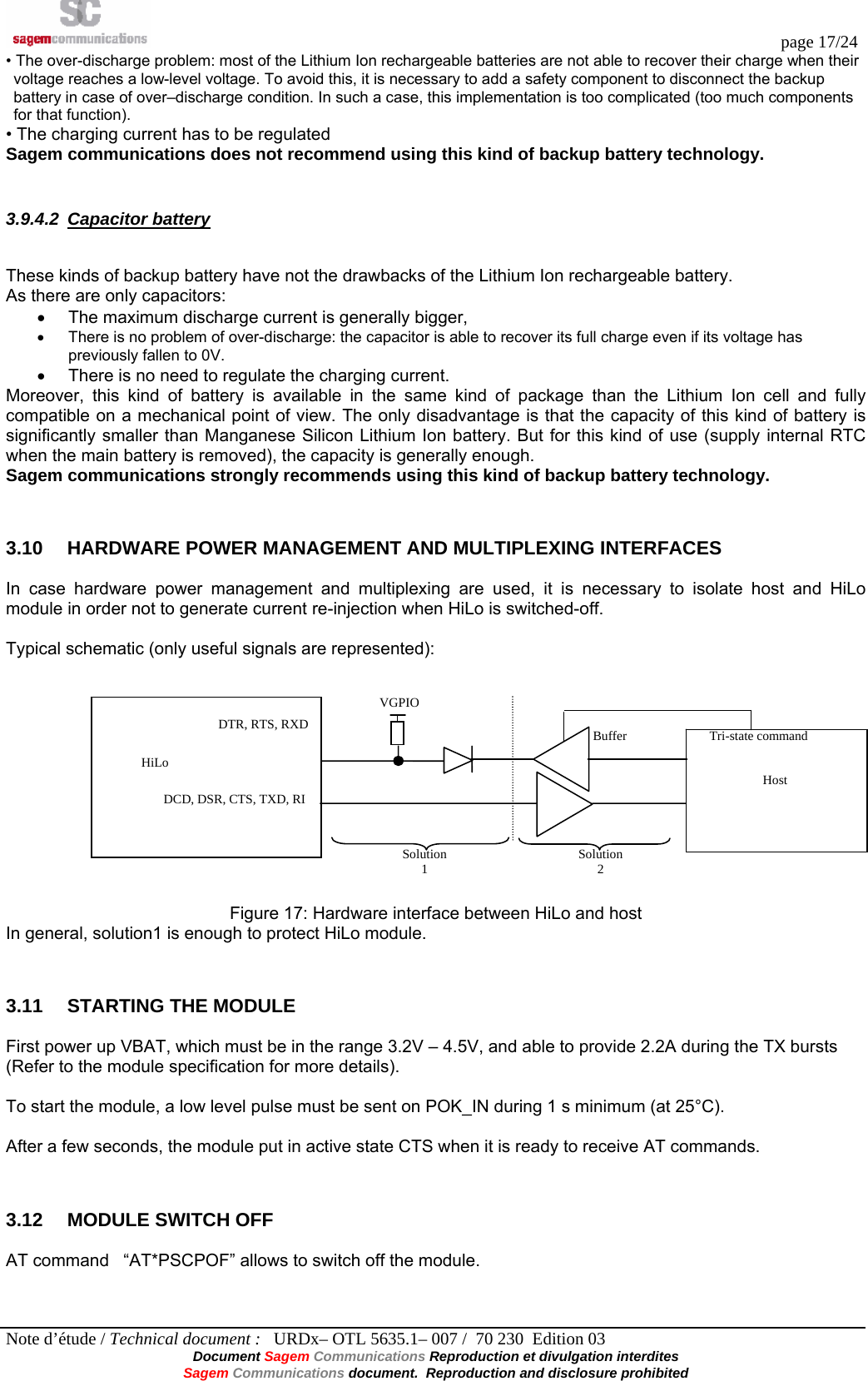
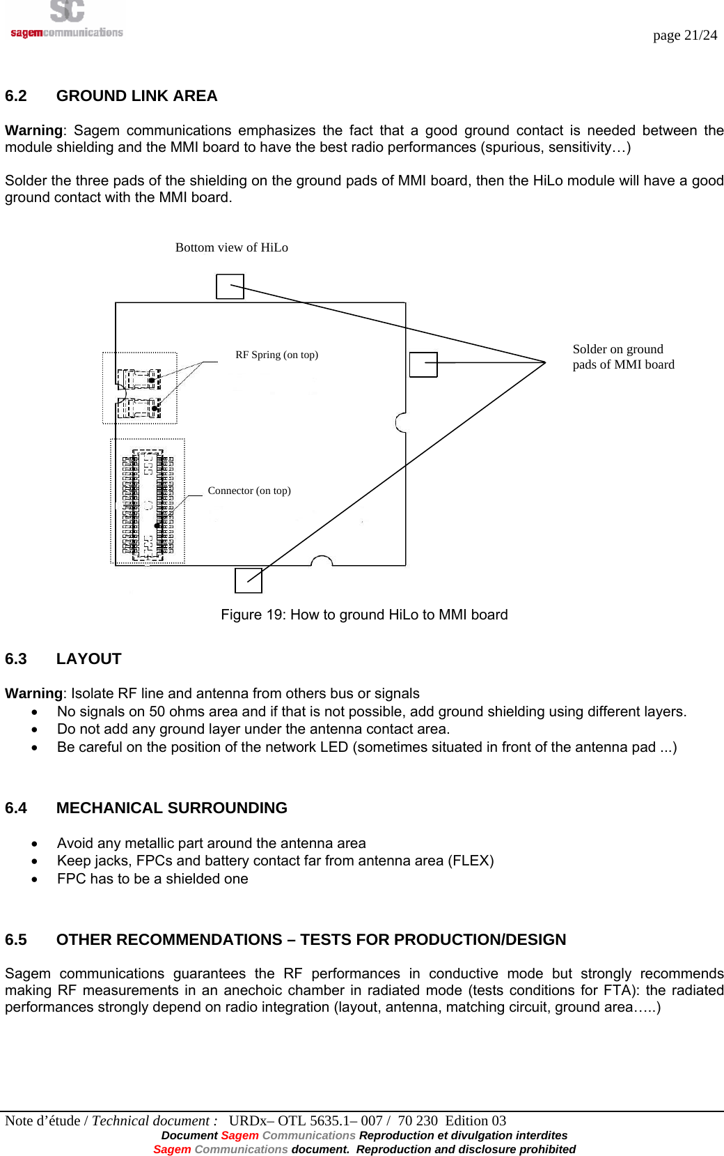
![page 12/24 Note d’étude / Technical document : URDx– OTL 5635.1– 007 / 70 230 Edition 03 Document Sagem Communications Reproduction et divulgation interdites Sagem Communications document. Reproduction and disclosure prohibited 3.5 EXAMPLE OF POWER SUPPLY 3.5.1 Example 1 It the following application note from Linear Technology LTC3440, this schematic is an example of a DC/DC power supply able to power 3.6V under 2.1A. This can be use with a AC/DC 5V unit or an USB or PCMCIA bus as input power source. Figure 9: Example of power supply based on a DC/DC step down converter 3.5.2 Example 2 If the whole power consumption is not an issue, this example of a voltage regulator used with an AC/DC 5V converter, can be used as a DC power supply. Figure 10: Example of power supply based on regulator The voltage output is given by: VOUT = 1.235V × [1 + (R1 / R2)] To have 3.7V out R1=560K & R2=271.8K (270K+1.8K)](https://usermanual.wiki/SAGEMCOM-BROANDS/HILOC/User-Guide-965316-Page-12.png)