SAGEMCOM BROANDS HILONC GSM/GPRS Module User Manual UserManual HiloNC
SAGEMCOM SAS GSM/GPRS Module UserManual HiloNC
UserManual.wiki
>
SAGEMCOM BROANDS
>
HILONC User Manual
>
User Manual
Contents
1.
User Manual
2.
Users Manual
User Manual
Navigation menu
Upload a User Manual
Namespaces
Wiki Guide
HTML
PDF
Info
Views
User Manual
Discussion / Help
Navigation
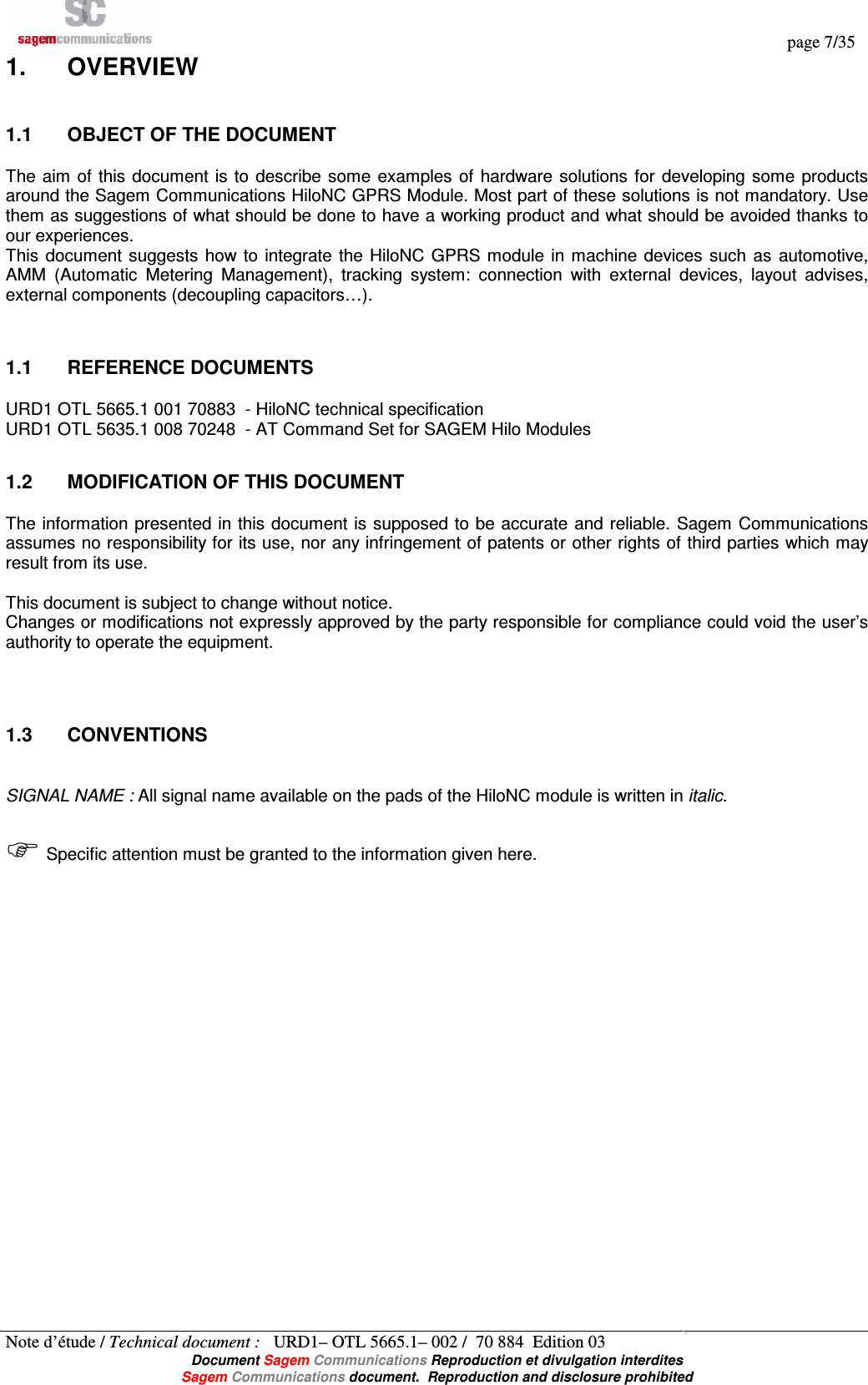
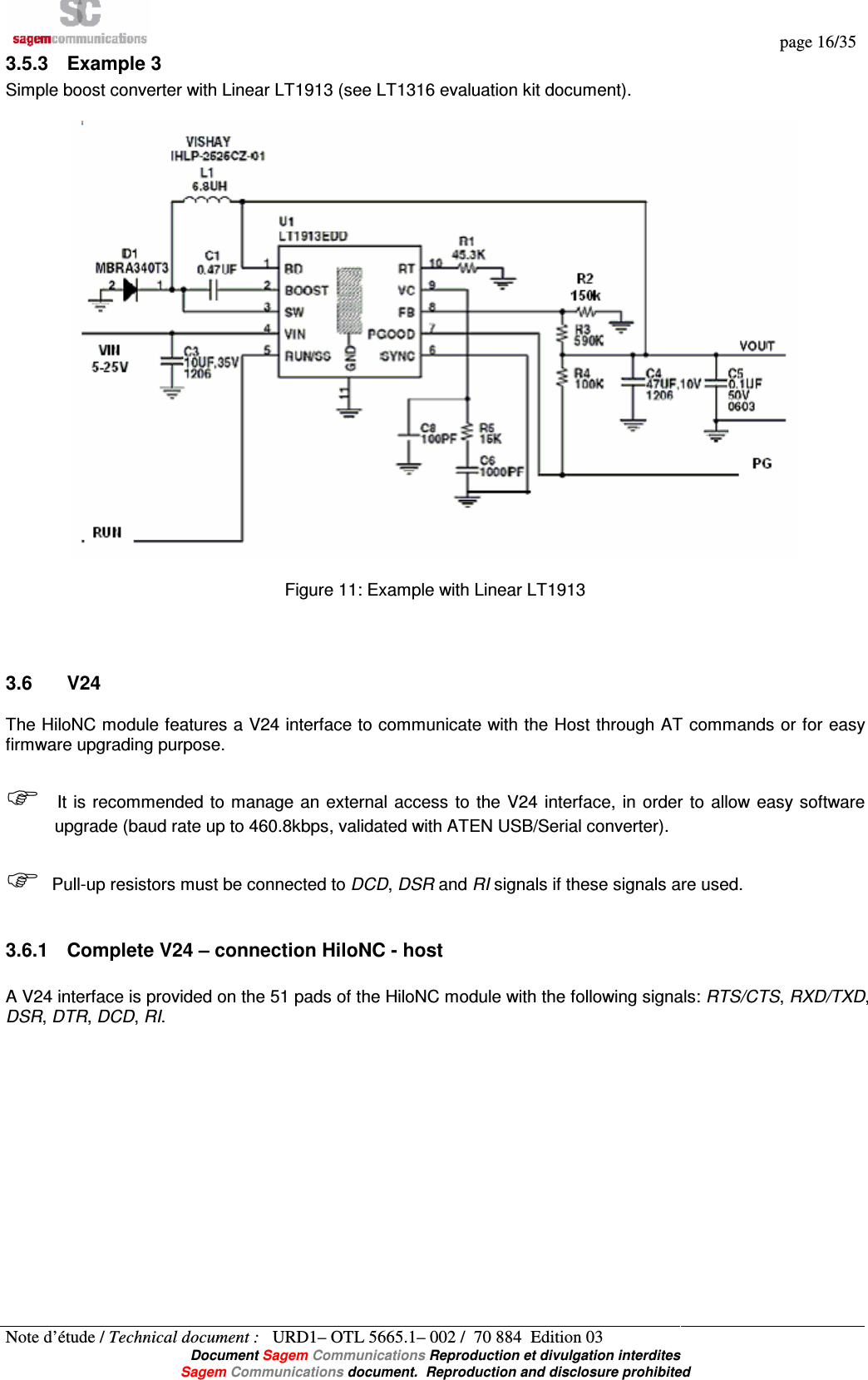
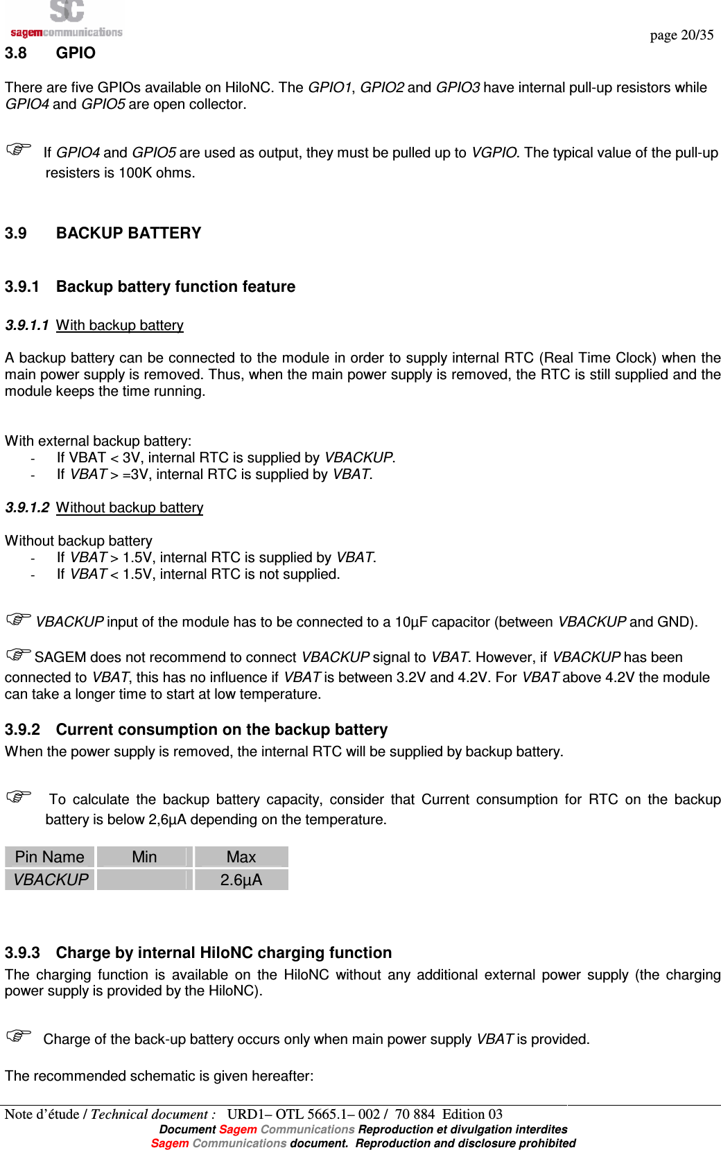
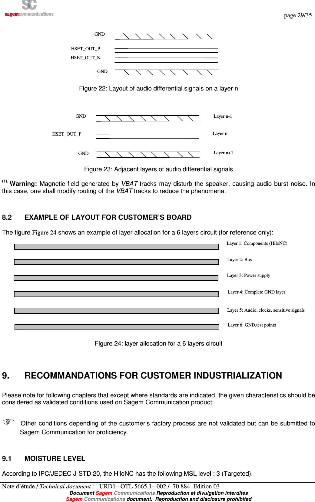
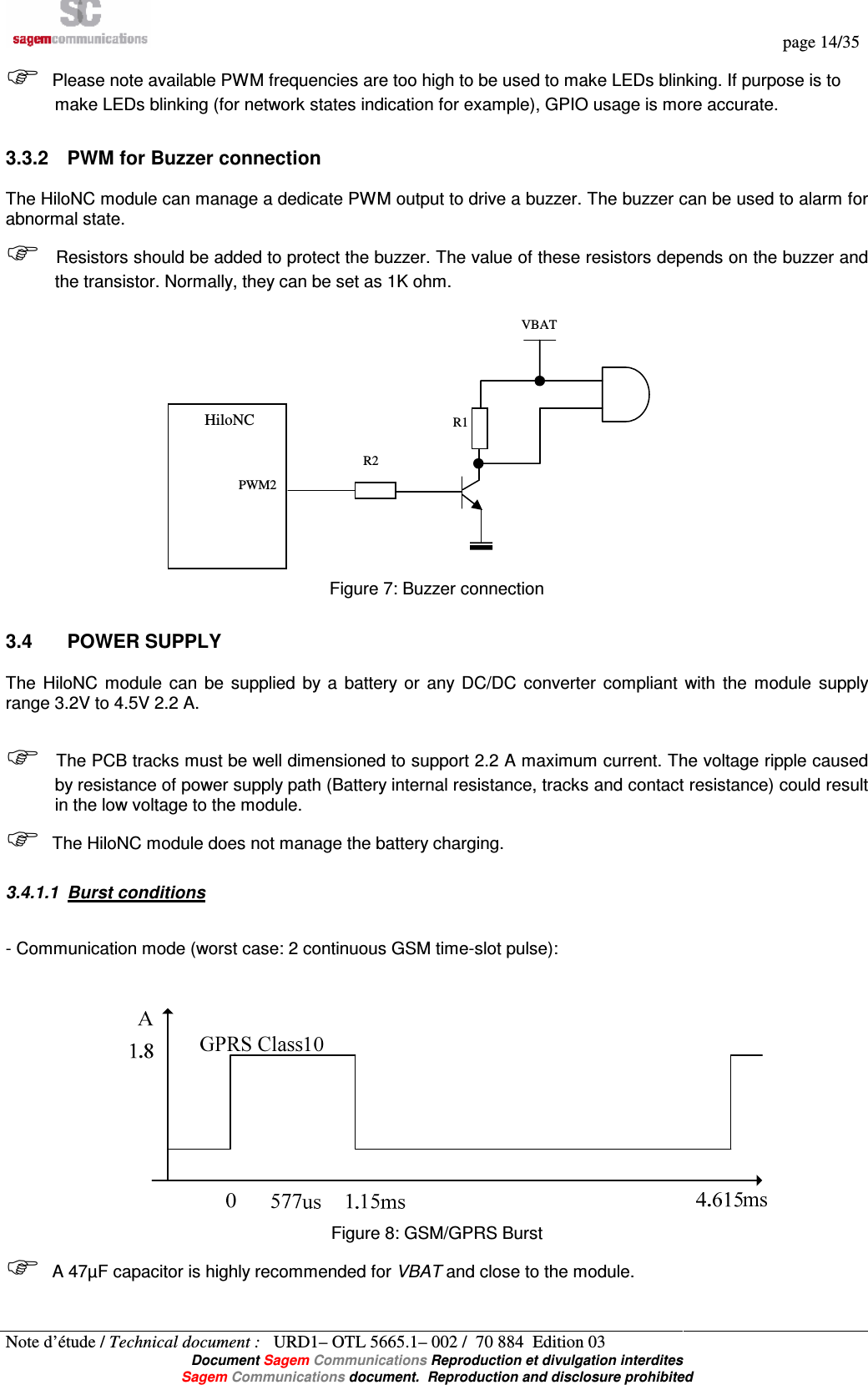
![page 8/35 Note d’étude / Technical document : URD1– OTL 5665.1– 002 / 70 884 Edition 03 Document Sagem Communications Reproduction et divulgation interdites Sagem Communications document. Reproduction and disclosure prohibited 2. BLOCK DIAGRAM PA + Switch850 /900 /1800 /1900(18 00MHz )(1 900 MHz )RFILRFIHRFOLRFOHFE _CTRLRamp _ DACRF SubsystemDCXO 26 MHzAntennapadEMC SubsystemExternal MemoryADDR[22 :1]DATA [15 :0]NCS _ RAMNCS _ FlashNUBNLBNOENWERTC32 .768 KHzADC SPIVBAT TTMS / RTCK / TCK / NTRST / TDI / TDO / TEST / TEST1 / TEST2AudioSubsystemGPIO SIM PWMPPPPEEEERRRRIIIIPPPPHHHHEEEERRRRAAAALLLLSSSSSIM _DATA / SIM _ CLK / SIM _RST / VSIMPWM [ 0:2]UARTRXD / RTS / CTS / TXD / DCD / DTR / DSR / RIIn OutSPI _ CLK / SPI _ IRQ / S PI _ OUT / SPI _ IN /SPI _SELINTMIC _BIASINTMIC _PHSET _ OUT _PHSET _OUT _N3 Pads8 Pads3 Pads4 Pads5 Pads1 PadGROUND3Pads3 +2 PadsJTAG9 PadsAUX _ADC 0VBACKUPPower Supply SystemVGPIOPOWERCONTROL1 Pad1 Pad1 PadPOK _ INVGPIOVBACKUPBand 1Band 2Dual Saw Filter (1800 /1900 )Band 1Band 2Dual Saw Filter (850 /900 )(850 MHz )(900 MHz )GPIO [ 1:5 ]5Pads1 PadRESETRESET Figure 1: Block diagram of HiloNC module](https://usermanual.wiki/SAGEMCOM-BROANDS/HILONC.User-Manual/User-Guide-1088212-Page-8.png)
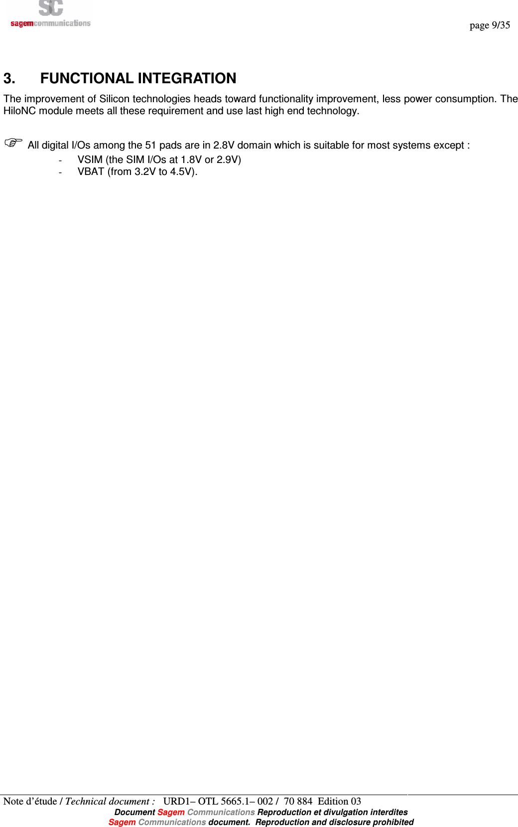
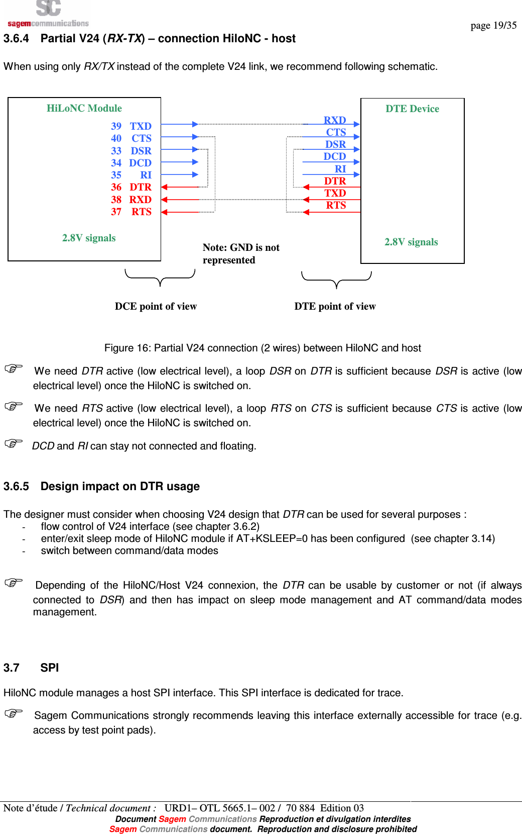
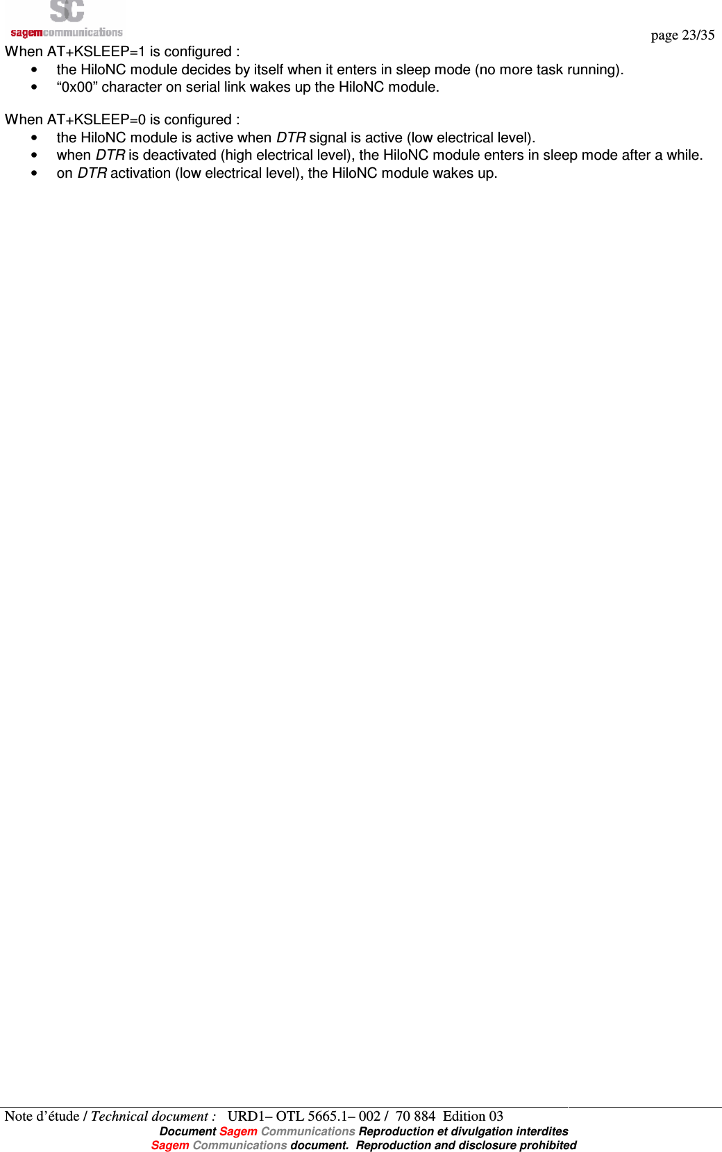
![page 15/35 Note d’étude / Technical document : URD1– OTL 5665.1– 002 / 70 884 Edition 03 Document Sagem Communications Reproduction et divulgation interdites Sagem Communications document. Reproduction and disclosure prohibited 3.5 EXAMPLE OF POWER SUPPLY 3.5.1 Example 1 It the following application note from Linear Technology LTC3440, this schematic is an example of a DC/DC power supply able to power 3.6V under 2.1A. This can be use with a AC/DC 5V unit or an USB or PCMCIA bus as input power source. Figure 9: Example of power supply based on a DC/DC step down converter 3.5.2 Example 2 If the whole power consumption is not an issue, this example of a voltage regulator used with an AC/DC 5V converter, can be used as a DC power supply. Figure 10: Example of power supply based on regulator The voltage output is given by: VOUT = 1.235V × [1 + (R1 / R2)] To have 3.7V out R1=560K & R2=271.8K (270K+1.8K)](https://usermanual.wiki/SAGEMCOM-BROANDS/HILONC.User-Manual/User-Guide-1088212-Page-15.png)