SAGEMCOM BROANDS HILONC GSM/GPRS Module User Manual UserManual HiloNC
SAGEMCOM SAS GSM/GPRS Module UserManual HiloNC
Contents
- 1. User Manual
- 2. Users Manual
User Manual
page 1/35
Note d’étude / Technical document : URD1– OTL 5665.1– 002 / 70 884 Edition 03
Document Sagem Communications Reproduction et divulgation interdites
Sagem Communications document. Reproduction and disclosure prohibited
Direction des Recherches et des Développements Etablissement de VELIZY
VELIZY R&D Center
NOTE D'ETUDE / TECHNICAL DOCUMENT
REFERENCE
URD1 – OTL 5665.1– 002 /
ETUDE / PROJECT
NOM DE L’ETUDE
70 884 Code C TA1
HiloNC Module
TITRE / TITLE :
HiloNC Application note
Edition Approbations /Approvals
N°
#
Rédacteur(s)
Author(s)
Chef de projet
Project design
manager
Responsable
d’entité /
Product design
manager
Chef Unité
R&D unit
manager
Assurance
Qualité /
R&D quality
assurance
03
Nom
Name
J.DUMONT T. Fu M. Boutboul E. Sillère
Date
27/06/08
Signature
RESUME / SUMMARY
This document is HiloNC module application note.
Mots clés / Keywords : Cellular, module, GSM, GPRS, application, M2M
√
√√
√
DIFFUSION INTERNE / INTERNAL DISTRIBUTION
REDACTEUR(S) / AUTHOR (S) + F.FREULON, F.GOUERE .
Distribution externe pour les prestataires de services : renseigner dans la rubrique ci-dessous sous la forme
« SOCIETE (P. Nom) »
DIFFUSION EXTERNE sous convention de confidentialité :
EXTERNAL DISTRIBUTION with confidentiality agreement :
………….
Enregistrement relatif à la qualité (ERQ) / Quality record
A déposer en enveloppe soleau / Put in a soleau envelope

page 2/35
Note d’étude / Technical document : URD1– OTL 5665.1– 002 / 70 884 Edition 03
Document Sagem Communications Reproduction et divulgation interdites
Sagem Communications document. Reproduction and disclosure prohibited
Direction des Recherches et des Développements Etablissement de VELIZY
VELIZY R&D Center
NOTE D'ETUDE / TECHNICAL DOCUMENT
FICHE RECAPITULATIVE / SUMMARY SHEET
Ed
Date
Date
Référence
Reference
Rédacteur(s)
Author(s)
Relecteur(s)
Reviser(s)
Pages modifiées
/ Changed pages
Observations
Comments
1
27/06/2008 URD1– OTL 5665.1–
002 / 70 884
Steven Long
Bingming Chen
Tiejun Fu / M.
Boutboul
Création du document /
Document creation
2
07/10/2008 URD1– OTL 5665.1–
002 / 70 884
AMMARI. M. DUMONT J. §3.6 and §3.10;
P25
UART Update
3
10/11/2008 URD1– OTL 5665.1–
002 / 70 884
AMMARI M. Dumont J. §3.1, §3.9, §3.12
Clarification on Vbackup
connection. Reset
duration 10ms. Sim card
connection figure 3.
page 3/35
Note d’étude / Technical document : URD1– OTL 5665.1– 002 / 70 884 Edition 03
Document Sagem Communications Reproduction et divulgation interdites
Sagem Communications document. Reproduction and disclosure prohibited
HiloNC Application Note

page 4/35
Note d’étude / Technical document : URD1– OTL 5665.1– 002 / 70 884 Edition 03
Document Sagem Communications Reproduction et divulgation interdites
Sagem Communications document. Reproduction and disclosure prohibited
Direction des Recherches et des Développements Etablissement de VELIZY
VELIZY R&D Center
SOMMAIRE / CONTENTS
Direction des Recherches et des Développements Etablissement de VELIZY................................................................1
NOTE D'ETUDE / TECHNICAL DOCUMENT.................................................................................................................1
Direction des Recherches et des Développements Etablissement de VELIZY................................................................2
NOTE D'ETUDE / TECHNICAL DOCUMENT.................................................................................................................2
FICHE RECAPITULATIVE / SUMMARY SHEET..........................................................................................................2
SOMMAIRE / CONTENTS .................................................................................................................................................4
FIGURES LIST ....................................................................................................................................................................6
1. OVERVIEW...................................................................................................................................................................7
1.1 OBJECT OF THE DOCUMENT.........................................................................................................................7
1.1 REFERENCE DOCUMENTS .............................................................................................................................7
1.2 MODIFICATION OF THIS DOCUMENT ..........................................................................................................7
1.3 CONVENTIONS ...................................................................................................................................................7
2. BLOCK DIAGRAM.......................................................................................................................................................8
3. FUNCTIONAL INTEGRATION...................................................................................................................................9
3.1 HOW TO CONNECT TO A SIM CARD..........................................................................................................10
3.2 HOW TO CONNECT THE AUDIOS? .............................................................................................................11
3.2.1 Connecting microphone and speaker .....................................................................................................11
3.2.2 Recommended characteristics for the microphone and speaker........................................................12
3.3 PWM ....................................................................................................................................................................13
3.3.1 PWM outputs ..................................................................................................................................................13
3.3.2 PWM for Buzzer connection.........................................................................................................................14
3.4 POWER SUPPLY ..............................................................................................................................................14
3.5 EXAMPLE OF POWER SUPPLY....................................................................................................................15
3.5.1 Example 1 ...................................................................................................................................................15
3.5.2 Example 2 ...................................................................................................................................................15
3.5.3 Example 3 ...................................................................................................................................................16
3.6 V24 .......................................................................................................................................................................16
3.6.1 Complete V24 – connection HiloNC - host .............................................................................................16
3.6.2 Complete V24 interface with PC ..............................................................................................................17
3.6.3 Partial V24 (RX-TX-RTS-CTS) – connection HiloNC - host.................................................................18
3.6.4 Partial V24 (RX-TX) – connection HiloNC - host ...................................................................................19
3.6.5 Design impact on DTR usage ..................................................................................................................19
3.7 SPI........................................................................................................................................................................19
3.8 GPIO ....................................................................................................................................................................20
3.9 BACKUP BATTERY...........................................................................................................................................20
3.9.1 Backup battery function feature ...............................................................................................................20
3.9.2 Current consumption on the backup battery ..........................................................................................20
3.9.3 Charge by internal HiloNC charging function .........................................................................................20
3.9.4 Backup Battery technology recommended.............................................................................................21
3.10 HARDWARE POWER MANAGEMENT AND MULTIPLEXING INTERFACES .......................................22
3.11 STARTING THE MODULE...............................................................................................................................22
3.12 MODULE RESET...............................................................................................................................................22
3.13 MODULE SWITCH OFF ...................................................................................................................................22
3.14 SLEEP MODE MANAGEMENT .......................................................................................................................22
4. MANDATORY POINTS FOR THE FINAL TESTS AND TUNING.........................................................................24
5. ESD & EMC RECOMMENDATIONS........................................................................................................................24
5.1 HILONC ALONE.................................................................................................................................................24
5.2 CUSTOMER’S PRODUCT WITH HILONC....................................................................................................24
5.2.1 Analysis........................................................................................................................................................24
5.2.2 Recommendations to avoid ESD issues.................................................................................................24
6. RADIO INTEGRATION..............................................................................................................................................25
6.1 ANTENNA ...........................................................................................................................................................25
6.2 GROUND LINK AREA.......................................................................................................................................25
6.3 LAYOUT ..............................................................................................................................................................25

page 5/35
Note d’étude / Technical document : URD1– OTL 5665.1– 002 / 70 884 Edition 03
Document Sagem Communications Reproduction et divulgation interdites
Sagem Communications document. Reproduction and disclosure prohibited
6.4 MECHANICAL SURROUNDING .....................................................................................................................26
6.5 OTHER RECOMMENDATIONS – TESTS FOR PRODUCTION/DESIGN ...............................................26
7. AUDIO INTEGRATION .............................................................................................................................................26
7.1 MECHANICAL INTEGRATION AND ACOUSTICS ......................................................................................26
7.2 ELECTRONICS AND LAYOUT........................................................................................................................27
8. RECOMMENDATIONS ON LAYOUT OF CUSTOMER’S BOARD.......................................................................28
8.1 GENERAL RECOMMENDATIONS ON LAYOUT .........................................................................................28
8.1.1 Ground.........................................................................................................................................................28
8.1.2 Power supplies ...........................................................................................................................................28
8.1.3 Clocks ..........................................................................................................................................................28
8.1.4 Data bus and other signals .......................................................................................................................28
8.1.5 Radio............................................................................................................................................................28
8.1.6 Audio (see also § 10.2)..............................................................................................................................28
8.2 EXAMPLE OF LAYOUT FOR CUSTOMER’S BOARD ................................................................................29
9. RECOMMANDATIONS FOR CUSTOMER INDUSTRIALIZATION .....................................................................29
9.1 MOISTURE LEVEL............................................................................................................................................29
9.2 PACKAGE...........................................................................................................................................................30
9.3 SOLDER MASK..................................................................................................................................................32
9.4 SOLDER PASTE................................................................................................................................................32
9.5 PROFILE FOR REFLOW SOLDERING .........................................................................................................32
9.6 SMT MACHINE ..................................................................................................................................................34
9.7 UNDERFILL ........................................................................................................................................................34
9.8 SECOND REFLOW SOLDERING...................................................................................................................35
9.9 HAND SOLDERING ..........................................................................................................................................35
9.10 REWORK ............................................................................................................................................................35
10. LABEL .....................................................................................................................................................................35

page 6/35
Note d’étude / Technical document : URD1– OTL 5665.1– 002 / 70 884 Edition 03
Document Sagem Communications Reproduction et divulgation interdites
Sagem Communications document. Reproduction and disclosure prohibited
FIGURES LIST
Figure 1: Block diagram of HiloNC module.............................................................................................................................8
Figure 2: SIM Card signals.....................................................................................................................................................10
Figure 3: Protections: EMC and ESD components close to the SIM......................................................................................10
Figure 4: Audio connection ....................................................................................................................................................11
Figure 5 : Filter and ESD protection of microphone...............................................................................................................12
Figure 6: Filter and ESD protection of 32 ohms speaker........................................................................................................12
Figure 7: Buzzer connection...................................................................................................................................................14
Figure 8: GSM/GPRS Burst ...................................................................................................................................................14
Figure 9: Example of power supply based on a DC/DC step down converter ........................................................................15
Figure 10: Example of power supply based on regulator........................................................................................................15
Figure 11: Example with Linear LT1913 ...............................................................................................................................16
Figure 12: Complete V24 connection between HiloNC and host ...........................................................................................17
Figure 13: connection to a data cable .....................................................................................................................................18
Figure 14: Partial V24 connection (4 wires) between HiloNC and host.................................................................................18
Figure 15: Partial V24 connection (2 wires) between HiloNC and host.................................................................................19
Figure 16: Backup battery internally charged.........................................................................................................................21
Figure 17: Charging curve of backup battery .........................................................................................................................21
Figure 18: Hardware interface between HiloNC and host ......................................................................................................22
Figure 19: Antenna connection...............................................................................................................................................25
Figure 20: Forbidden area for via ...........................................................................................................................................26
Figure 21: Layout of audio differential signals on a layer n ...................................................................................................29
Figure 22: Adjacent layers of audio differential signals .........................................................................................................29
Figure 23: layer allocation for a 6 layers circuit .....................................................................................................................29
Figure 24 : Solder mask design...............................................................................................................................................32
Figure 25 : Typical thermal profile.........................................................................................................................................33
Figure 26 : CMS fiducials positions .......................................................................................................................................34
Figure 27 : Underfill holes......................................................................................................................................................35

page 7/35
Note d’étude / Technical document : URD1– OTL 5665.1– 002 / 70 884 Edition 03
Document Sagem Communications Reproduction et divulgation interdites
Sagem Communications document. Reproduction and disclosure prohibited
1. OVERVIEW
1.1 OBJECT OF THE DOCUMENT
The aim of this document is to describe some examples of hardware solutions for developing some products
around the Sagem Communications HiloNC GPRS Module. Most part of these solutions is not mandatory. Use
them as suggestions of what should be done to have a working product and what should be avoided thanks to
our experiences.
This document suggests how to integrate the HiloNC GPRS module in machine devices such as automotive,
AMM (Automatic Metering Management), tracking system: connection with external devices, layout advises,
external components (decoupling capacitors…).
1.1 REFERENCE DOCUMENTS
URD1 OTL 5665.1 001 70883 - HiloNC technical specification
URD1 OTL 5635.1 008 70248 - AT Command Set for SAGEM Hilo Modules
1.2 MODIFICATION OF THIS DOCUMENT
The information presented in this document is supposed to be accurate and reliable. Sagem Communications
assumes no responsibility for its use, nor any infringement of patents or other rights of third parties which may
result from its use.
This document is subject to change without notice.
Changes or modifications not expressly approved by the party responsible for compliance could void the user’s
authority to operate the equipment.
1.3 CONVENTIONS
SIGNAL NAME : All signal name available on the pads of the HiloNC module is written in italic.
Specific attention must be granted to the information given here.
page 8/35
Note d’étude / Technical document : URD1– OTL 5665.1– 002 / 70 884 Edition 03
Document Sagem Communications Reproduction et divulgation interdites
Sagem Communications document. Reproduction and disclosure prohibited
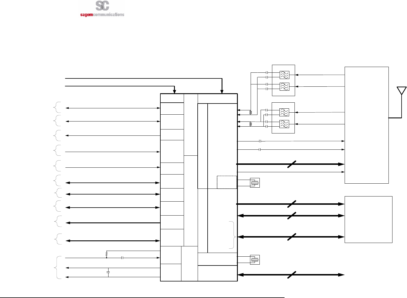
2. BLOCK DIAGRAM
PA + Switch
850 /900 /1800 /1900
(18 00MHz )
(1 900 MHz )
RFIL
RFIH
RFOL
RFOH
FE _CTRL
Ramp _ DAC
RF Subsystem
DCXO 26 MHz
Antenna
pad
EMC Subsystem
External Memory
ADDR
[22 :1]
DATA [15 :0]
NCS _ RAM
NCS _ Flash
NUB
NLB
NOE
NWE
RTC
32 .768 KHz
ADC SPI
VBAT T
TMS / RTCK / TCK / NTRST / TDI / TDO / TEST / TEST1 / TEST2
Audio
Subsystem
GPIO SIM PWM
P
P
P
PE
E
E
ER
R
R
RI
I
I
IP
P
P
PH
H
H
HE
E
E
ER
R
R
RA
A
A
AL
L
L
LS
S
S
S
SIM _DATA / SIM _ CLK / SIM _RST / VSIM
PWM [ 0:2]
UART
RXD / RTS / CTS / TXD / DCD / DTR / DSR / RI
In Out
SPI _ CLK / SPI _ IRQ / S PI _ OUT / SPI _ IN /
SPI _SEL
INTMIC _BIAS
INTMIC _P
HSET _ OUT _P
HSET _OUT _N
3 Pads
8 Pads
3 Pads
4 Pads
5 Pads
1 Pad
GROUND
3Pads
3 +2 Pads
JTAG
9 Pads
AUX _ADC 0
VBA
CK
UP
Power Supply System
VGPIO
POWER
CONTROL
1 Pad
1 Pad
1 Pad
POK _ IN
VGPIO
VBACKUP
Band 1
Band 2
Dual Saw Filter (1800 /1900 )
Band 1
Band 2
Dual Saw Filter (850 /900 )
(850 MHz )
(900 MHz )
GPIO [ 1:5 ]
5Pads
1 Pad
RESET
RESET
Figure 1: Block diagram of HiloNC module

page 9/35
Note d’étude / Technical document : URD1– OTL 5665.1– 002 / 70 884 Edition 03
Document Sagem Communications Reproduction et divulgation interdites
Sagem Communications document. Reproduction and disclosure prohibited
3. FUNCTIONAL INTEGRATION
The improvement of Silicon technologies heads toward functionality improvement, less power consumption. The
HiloNC module meets all these requirement and use last high end technology.
All digital I/Os among the 51 pads are in 2.8V domain which is suitable for most systems except :
- VSIM (the SIM I/Os at 1.8V or 2.9V)
- VBAT (from 3.2V to 4.5V).
page 10/35
Note d’étude / Technical document : URD1– OTL 5665.1– 002 / 70 884 Edition 03
Document Sagem Communications Reproduction et divulgation interdites
Sagem Communications document. Reproduction and disclosure prohibited
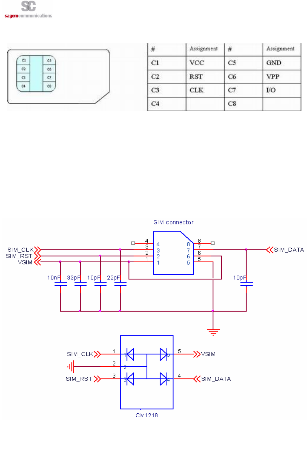
3.1 HOW TO CONNECT TO A SIM CARD
Figure 2: SIM Card signals
HiloNC module provides the SIM signals on the 51 pads. A SIM card holder with 6 pads needs to be adopted to
use the SIM function.
Decoupling capacitors have to be added on SIM_CLK, SIM_RST, VSIM and SIM_DATA signals as close
as possible to the SIM card connector to avoid EMC issues.
Use ESD protection components to protect SIM card and module I/Os against Electro Static Discharges.
The following schematic show how to protect the SIM access for 6 pads connector.
Figure 3: Protections: EMC and ESD components close to the SIM
page 11/35
Note d’étude / Technical document : URD1– OTL 5665.1– 002 / 70 884 Edition 03
Document Sagem Communications Reproduction et divulgation interdites
Sagem Communications document. Reproduction and disclosure prohibited
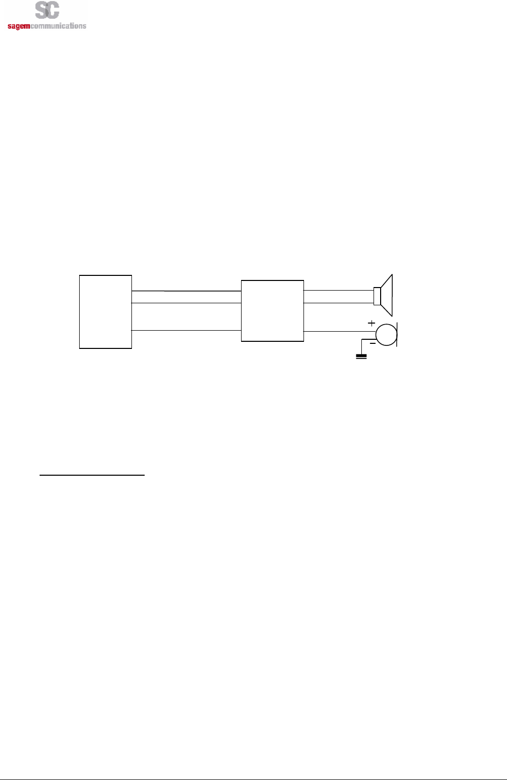
3.2 HOW TO CONNECT THE AUDIOS?
The HiloNC module features one input audio path and one output audio path. The input path is single-end while
the output path is differential. In this following chapter examples of design will be given including protections
against EMC and ESD and some notes about the routing rules to follow to avoid the TDMA noise usually present
in this sensitive area of design.
Please note that acoustic competences are mandatory to get accurate audio performance on customer’s
product.
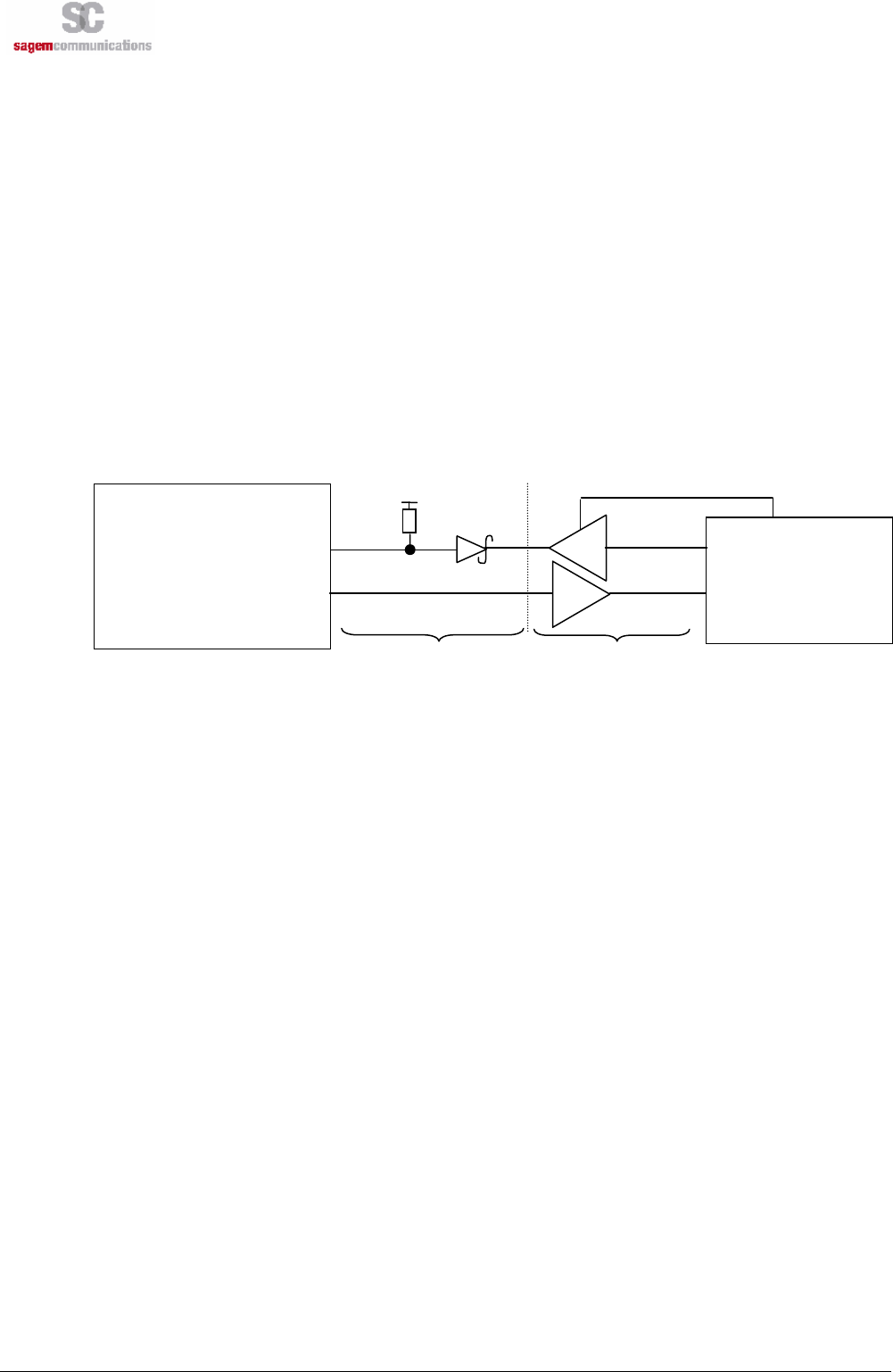
3.2.1 Connecting microphone and speaker
The HiloNC module can manage an external microphone (INTMIC_P) in single-end mode and an external
speaker (HSET_OUT_P / HSET_OUT_N) in differential mode. Thus, one speaker and one microphone can be
connected to the module. The bias supply to microphone is implemented in the module.
The speaker connected to the module should be 32 ohms.
Figure 4: Audio connection
If the design is ESD or EMC sensitive we strongly recommend to read the notes below.
The weakness can either come from the PCB routing and placement or from the chosen components (or both).
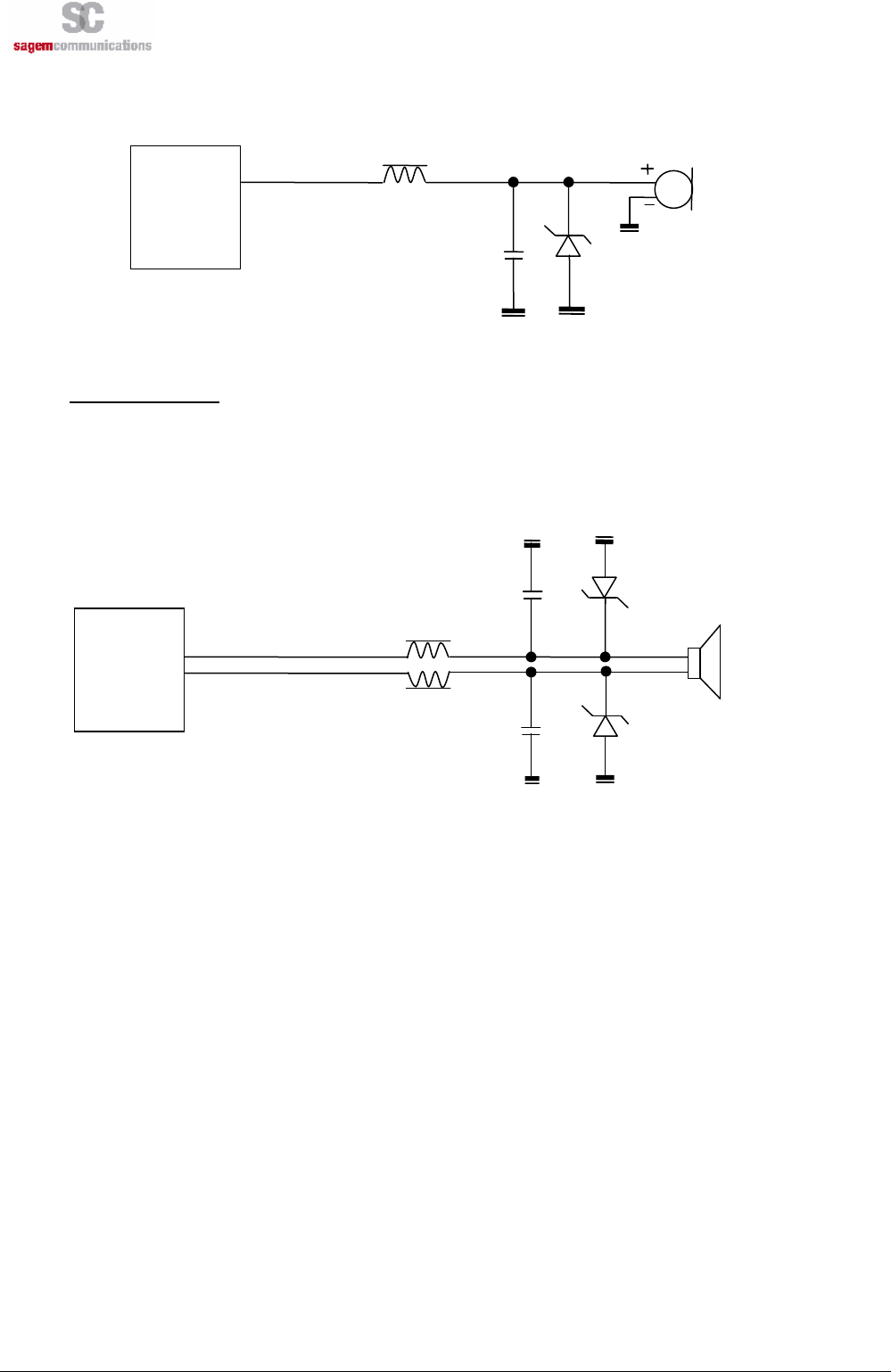
3.2.1.1 Notes for microphone
Pay attention to the microphone device, it must not be sensitive to RF disturbances.
Some microphones include two spatial microphones inside the same shell and allow to make an electrical
difference between the environment noise (received by one of the two mic.) and the active signal
(received by the other mic. + noise) resulting in a very high SNR.
If you need to have deported microphone out of the board with long wires, you should pay attention to the
EMC and ESD effect. It is also the case when your design is ESD sensitive. In those cases, add the
following protections to improve your design.
To ensure proper operation of such sensitive signals, they have to be isolated from the others by analogue
ground on customer’s board layout. (Refer to Layout design chapter)
HiloNC Filter and
ESD
protection
HSET_OUT_P
HSET_OUT_N
INTMIC_P
32ohms speaker
MIC
page 12/35
Note d’étude / Technical document : URD1– OTL 5665.1– 002 / 70 884 Edition 03
Document Sagem Communications Reproduction et divulgation interdites
Sagem Communications document. Reproduction and disclosure prohibited
Figure 5 : Filter and ESD protection of microphone
3.2.1.2 Notes for speaker
As explained for the microphone, if the speaker is deported out of the board or is sensitive to ESD, use the
schematic here after to improve the audio.
Figure 6: Filter and ESD protection of 32 ohms speaker
HSET_OUT_P, HSET_OUT_N tracks must be larger than other tracks: 0.1 mm.
As described in the layout chapter, differential signals have to be routed in parallel (HSET_OUT_P and
HSET_OUT_N signals)
The impedance of audio chain (filter + speaker) must be lower than 32 Ohm.
3.2.2 Recommended characteristics for the microphone and speaker
HiloNC
INTMIC_P
MIC
Ferrite Bead
18pF
ESD protection
HiloNC HSET_OUT_P
HSET_OUT_N
speaker
Ferrite Bead
Ferrite Bead
18pF
18pF
ESD protection
ESD protection
page 13/35
Note d’étude / Technical document : URD1– OTL 5665.1– 002 / 70 884 Edition 03
Document Sagem Communications Reproduction et divulgation interdites
Sagem Communications document. Reproduction and disclosure prohibited
3.2.2.1 Recommended characteristics for the microphone
Item to be inspected Acceptance criterion
Sensitivity - 40 dB SPL +/-3 dB (0 dB = 1 V/Pa @ 1kHz)
Frequency response Limits (relatives values)
Freq. (Hz) Lower limit Upper limit
100 -1 1
200 -1 1
300 -1 1
1000 0 0
2000 -1 1
3000 -1.5 1.5
3400 -2 2
4000 -2 2
Current consumption 1 mA (maximum)
Operating voltage DC 1 to 3 V (minimum)
S / N ratio 55 dB minimum (A-Curve at 1 kHz, 1 Pa)
Directivity Omni-directional
Maximum input sound pressure level
100 dB SPL (1 kHz)
Maximum distortion 1%
Radio frequency protection Over 800 -1200 MHz and 1700 -2000 MHz, S/N ratio 50
dB minimum (signal 1 kHz, 1 Pa)
3.2.2.2 Recommended characteristics for the speaker
Item to be inspected Acceptance criterion
Input power: rated / max 0.1W (Rate)
Audio chain impedance 32 ohm +/- 10% at 1V 1KHz
Frequency Range 300 Hz ~ 4.0 KHz
Sensitivity (S.P.L) >105 dB at 1KHz with IEC318 coupler,
Distortion 5% max at 1K Hz, nominal input power
3.3 PWM
3.3.1 PWM outputs
The HiloNC module can manage two PWM outputs.
They can be configured with appropriate AT command (for more details refer to AT command set for Sagem
HiloNC module specification).
User application can set for each output:
- Frequency between : 25.6KHz and 1083.3KHz
- Duty range from: 0 to 100%
page 14/35
Note d’étude / Technical document : URD1– OTL 5665.1– 002 / 70 884 Edition 03
Document Sagem Communications Reproduction et divulgation interdites
Sagem Communications document. Reproduction and disclosure prohibited
Please note available PWM frequencies are too high to be used to make LEDs blinking. If purpose is to
make LEDs blinking (for network states indication for example), GPIO usage is more accurate.
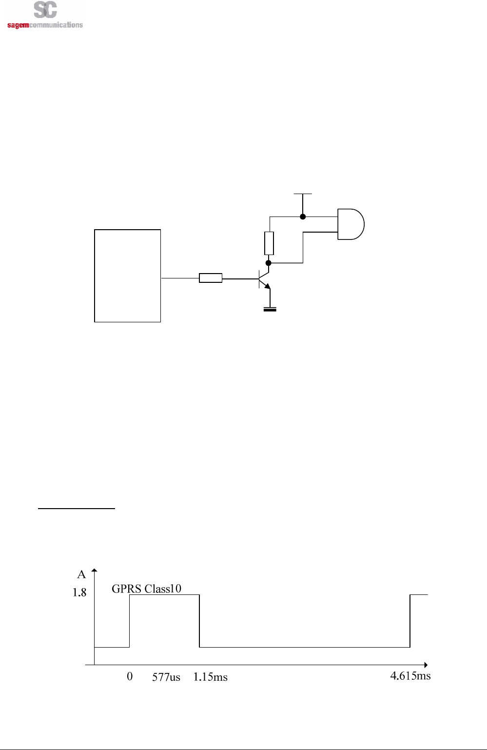
3.3.2 PWM for Buzzer connection
The HiloNC module can manage a dedicate PWM output to drive a buzzer. The buzzer can be used to alarm for
abnormal state.
Resistors should be added to protect the buzzer. The value of these resistors depends on the buzzer and
the transistor. Normally, they can be set as 1K ohm.
Figure 7: Buzzer connection
3.4 POWER SUPPLY
The HiloNC module can be supplied by a battery or any DC/DC converter compliant with the module supply
range 3.2V to 4.5V 2.2 A.
The PCB tracks must be well dimensioned to support 2.2 A maximum current. The voltage ripple caused
by resistance of power supply path (Battery internal resistance, tracks and contact resistance) could result
in the low voltage to the module.
The HiloNC module does not manage the battery charging.
3.4.1.1 Burst conditions
- Communication mode (worst case: 2 continuous GSM time-slot pulse):
Figure 8: GSM/GPRS Burst
A 47µF capacitor is highly recommended for VBAT and close to the module.
R1
R2
HiloNC
VBAT
PWM2
page 15/35
Note d’étude / Technical document : URD1– OTL 5665.1– 002 / 70 884 Edition 03
Document Sagem Communications Reproduction et divulgation interdites
Sagem Communications document. Reproduction and disclosure prohibited
3.5 EXAMPLE OF POWER SUPPLY
3.5.1 Example 1
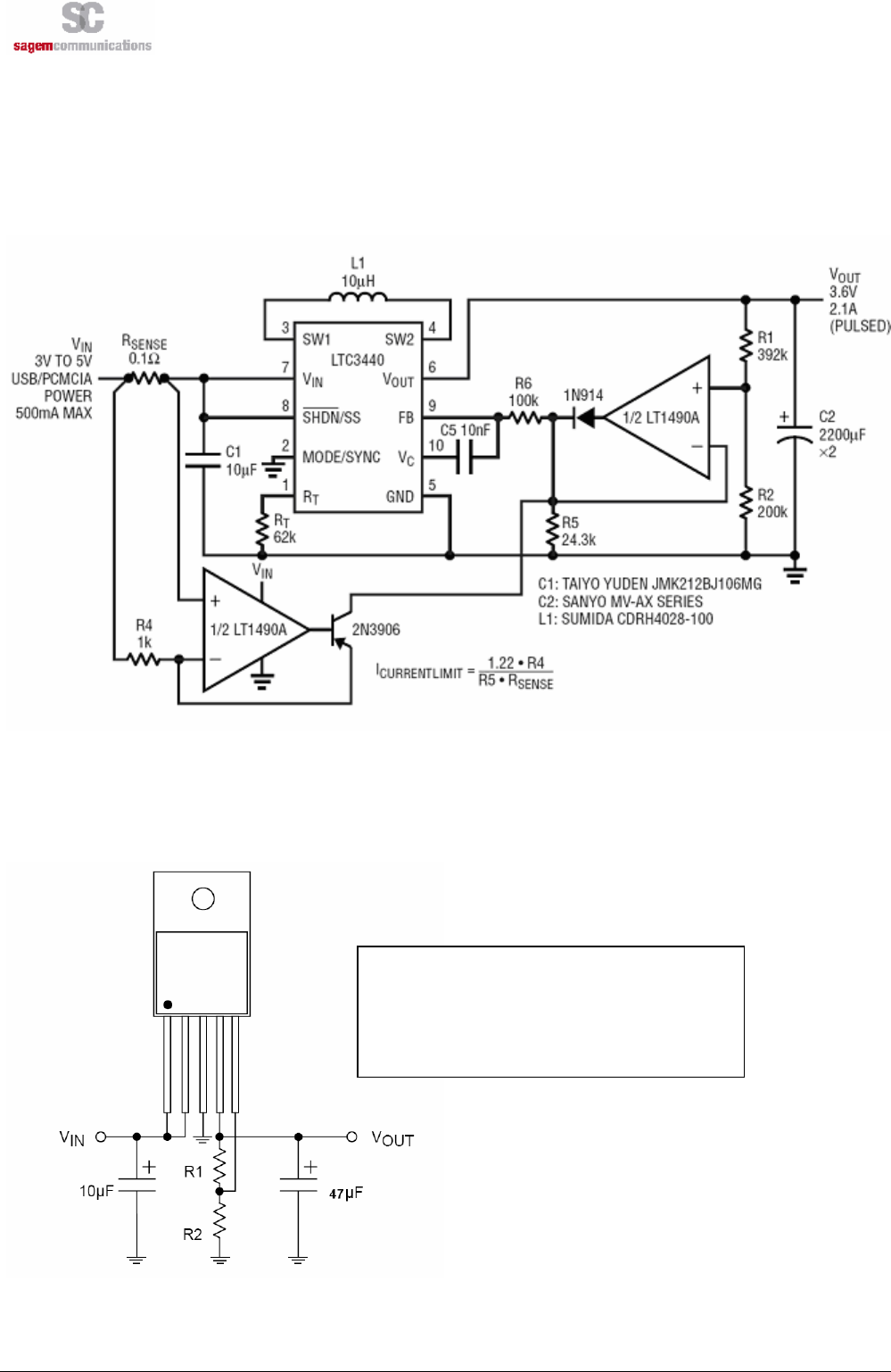
It the following application note from Linear Technology LTC3440, this schematic is an example of a DC/DC
power supply able to power 3.6V under 2.1A. This can be use with a AC/DC 5V unit or an USB or PCMCIA bus
as input power source.
Figure 9: Example of power supply based on a DC/DC step down converter
3.5.2 Example 2
If the whole power consumption is not an issue, this example of a voltage regulator used with an AC/DC 5V
converter, can be used as a DC power supply.
Figure 10: Example of power supply based on regulator
The voltage output is given by:
VOUT = 1.235V × [1 + (R1 / R2)]
To have 3.7V out R1=560K & R2=271.8K
(270K+1.8K)
page 16/35
Note d’étude / Technical document : URD1– OTL 5665.1– 002 / 70 884 Edition 03
Document Sagem Communications Reproduction et divulgation interdites
Sagem Communications document. Reproduction and disclosure prohibited
3.5.3 Example 3
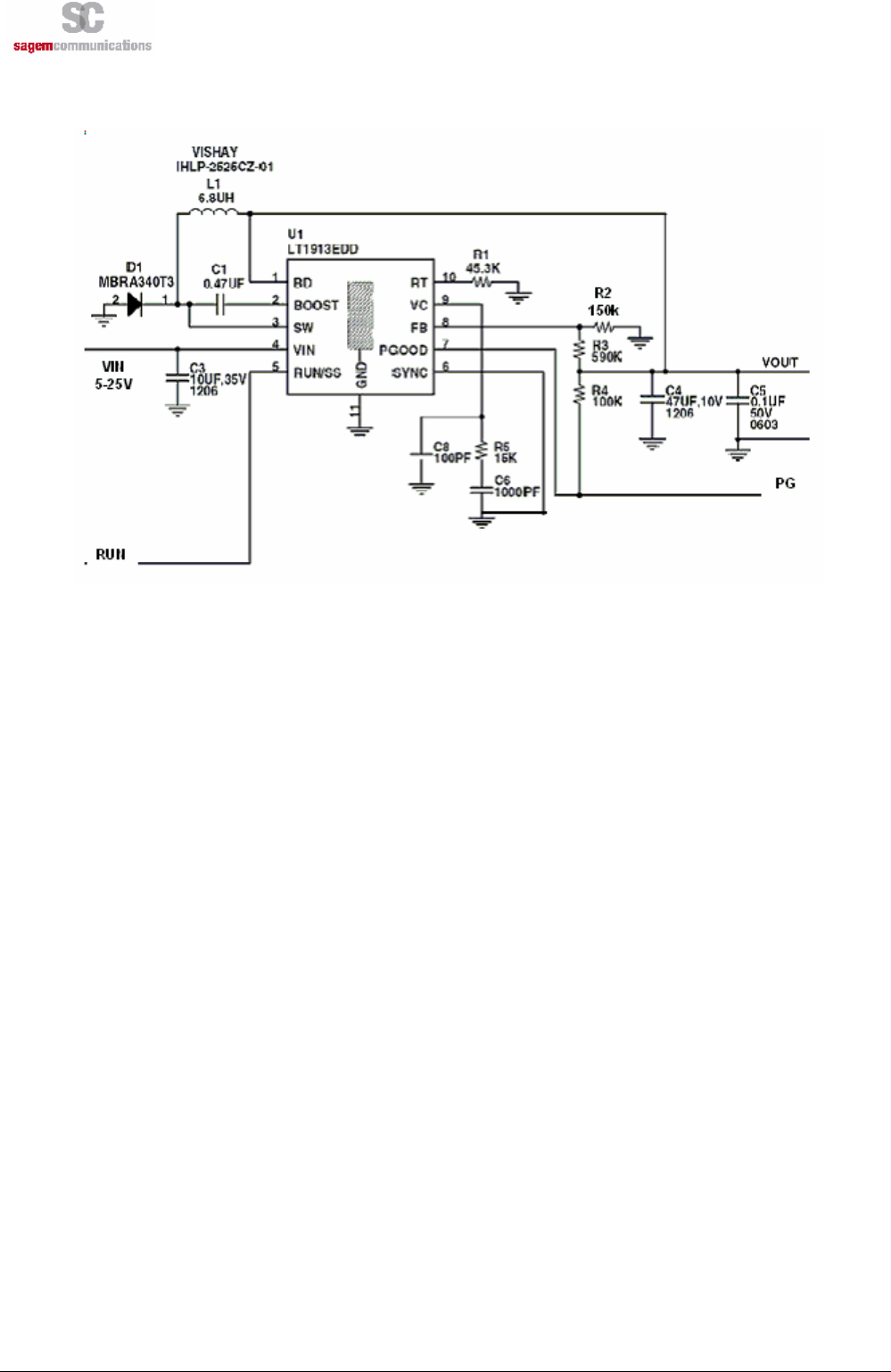
Simple boost converter with Linear LT1913 (see LT1316 evaluation kit document).
Figure 11: Example with Linear LT1913
3.6 V24
The HiloNC module features a V24 interface to communicate with the Host through AT commands or for easy
firmware upgrading purpose.
It is recommended to manage an external access to the V24 interface, in order to allow easy software
upgrade (baud rate up to 460.8kbps, validated with ATEN USB/Serial converter).
Pull-up resistors must be connected to DCD, DSR and RI signals if these signals are used.
3.6.1 Complete V24 – connection HiloNC - host
A V24 interface is provided on the 51 pads of the HiloNC module with the following signals: RTS/CTS, RXD/TXD,
DSR, DTR, DCD, RI.
page 17/35
Note d’étude / Technical document : URD1– OTL 5665.1– 002 / 70 884 Edition 03
Document Sagem Communications Reproduction et divulgation interdites
Sagem Communications document. Reproduction and disclosure prohibited
Figure 12: Complete V24 connection between HiloNC and host
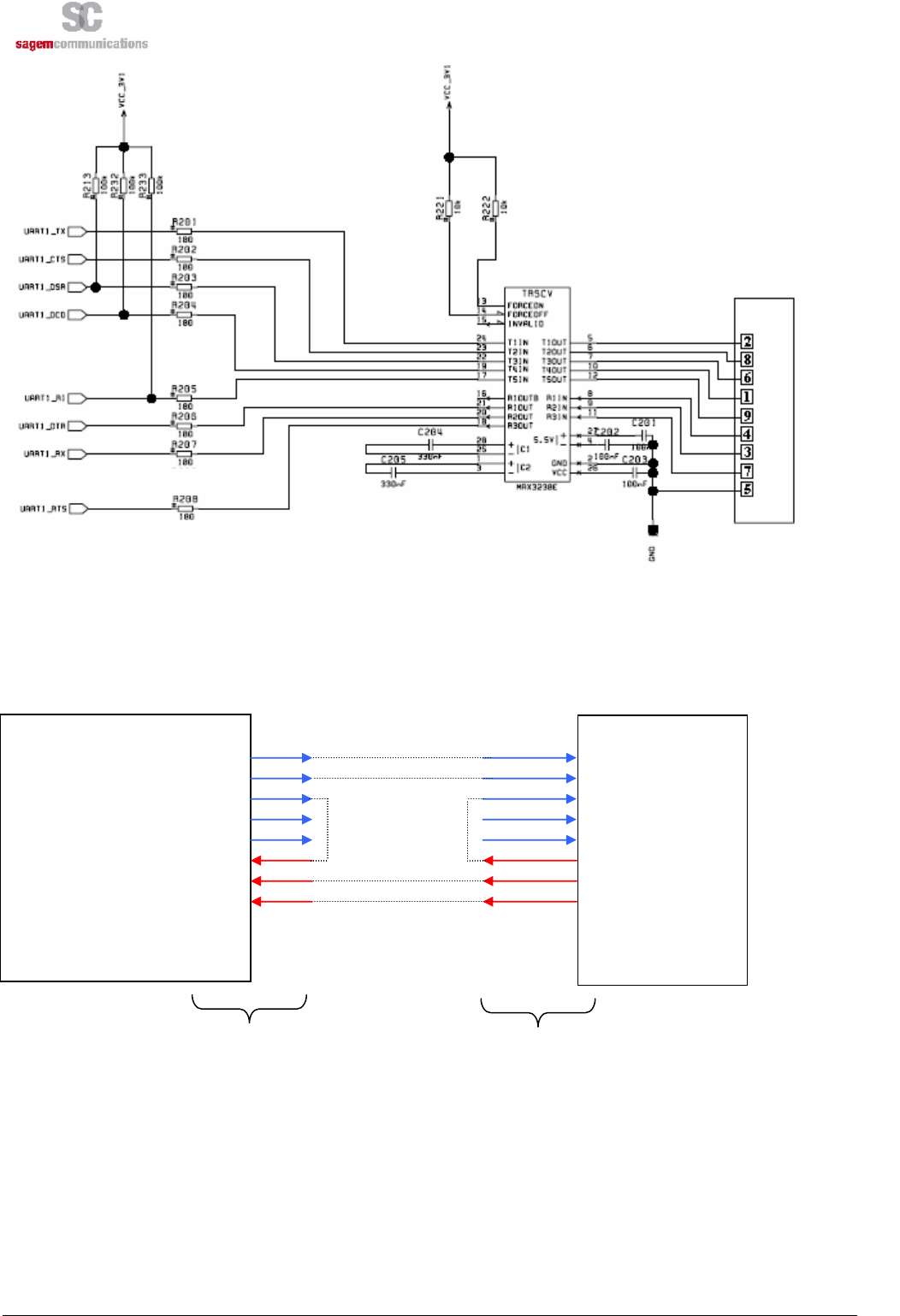
3.6.2 Complete V24 interface with PC
It supports speeds up to 115.2 Kbps and may be used in auto bauding mode.
To use the V24 interface, some adaptation components are necessary to convert the +2.8V signals from the
HiloNC to +/- 5V signals compatible with a PC.
Figure 13: connection to a data cable
To create your own data cable (for software download purpose…etc…) please refer to the following schematic
as an example:
DCE point of view DTE point of view
RXD
CTS
DSR
DCD
RI
DTR
TXD
RTS
HiLoNC Module
TXD
CTS
DSR
DCD
RI
DTR
RXD
RTS
DTE Device
2.8V signals
39
40
33
34
35
36
38
37
2.8V signals
Note: GND is not
represented
RXD
CTS
DSR
DCD
RI
DTR
TXD
RTS
HiLoNC Module
TXD
CTS
DSR
DCD
RI
DTR
RXD
RTS
RS232 Transceiver
IN
IN
IN
IN
IN
OUT
OUT
OUT
OUT
OUT
OUT
OUT
OUT
IN
IN
IN
DCE point of view DTE point of view
SUBD9 Female
Note: pin 5 is GND
1
6
9
5
2
8
6
1
9
4
3
7
2.8V signals 3.1V to +/-5.5V
signals
39
40
33
34
35
36
38
37
page 18/35
Note d’étude / Technical document : URD1– OTL 5665.1– 002 / 70 884 Edition 03
Document Sagem Communications Reproduction et divulgation interdites
Sagem Communications document. Reproduction and disclosure prohibited
Figure 14: Example of a connection to a data cable
3.6.3 Partial V24 (RX-TX-RTS-CTS) – connection HiloNC - host
When using only RX/TX/RTS/CTS instead of the complete V24 link, we recommend following schematic.
Figure 15: Partial V24 connection (4 wires) between HiloNC and host
As we need DTR active (low electrical level), a loop DSR on DTR is sufficient because DSR is active (low
electrical level) once the HiloNC is switched on.
DCD and RI can stay not connected and floating.
RXD
CTS
DSR
DCD
RI
DTR
TXD
RTS
HiLoNC Module
TXD
CTS
DSR
DCD
RI
DTR
RXD
RTS
DTE Device
2.8V signals
39
40
33
34
35
36
38
37
2.8V signals
Note: GND is not
represented
page 19/35
Note d’étude / Technical document : URD1– OTL 5665.1– 002 / 70 884 Edition 03
Document Sagem Communications Reproduction et divulgation interdites
Sagem Communications document. Reproduction and disclosure prohibited
3.6.4 Partial V24 (RX-TX) – connection HiloNC - host
When using only RX/TX instead of the complete V24 link, we recommend following schematic.
Figure 16: Partial V24 connection (2 wires) between HiloNC and host
We need DTR active (low electrical level), a loop DSR on DTR is sufficient because DSR is active (low
electrical level) once the HiloNC is switched on.
We need RTS active (low electrical level), a loop RTS on CTS is sufficient because CTS is active (low
electrical level) once the HiloNC is switched on.
DCD and RI can stay not connected and floating.
3.6.5 Design impact on DTR usage
The designer must consider when choosing V24 design that DTR can be used for several purposes :
- flow control of V24 interface (see chapter 3.6.2)
- enter/exit sleep mode of HiloNC module if AT+KSLEEP=0 has been configured (see chapter 3.14)
- switch between command/data modes
Depending of the HiloNC/Host V24 connexion, the DTR can be usable by customer or not (if always
connected to DSR) and then has impact on sleep mode management and AT command/data modes
management.
3.7 SPI
HiloNC module manages a host SPI interface. This SPI interface is dedicated for trace.
Sagem Communications strongly recommends leaving this interface externally accessible for trace (e.g.
access by test point pads).
DCE point of view DTE point of view
RXD
CTS
DSR
DCD
RI
DTR
TXD
RTS
HiLoNC Module
TXD
CTS
DSR
DCD
RI
DTR
RXD
RTS
DTE Device
2.8V signals
39
40
33
34
35
36
38
37
2.8V signals
Note: GND is not
represented

page 20/35
Note d’étude / Technical document : URD1– OTL 5665.1– 002 / 70 884 Edition 03
Document Sagem Communications Reproduction et divulgation interdites
Sagem Communications document. Reproduction and disclosure prohibited
3.8 GPIO
There are five GPIOs available on HiloNC. The GPIO1, GPIO2 and GPIO3 have internal pull-up resistors while
GPIO4 and GPIO5 are open collector.
If GPIO4 and GPIO5 are used as output, they must be pulled up to VGPIO. The typical value of the pull-up
resisters is 100K ohms.
3.9 BACKUP BATTERY
3.9.1 Backup battery function feature
3.9.1.1 With backup battery
A backup battery can be connected to the module in order to supply internal RTC (Real Time Clock) when the
main power supply is removed. Thus, when the main power supply is removed, the RTC is still supplied and the
module keeps the time running.
With external backup battery:
- If VBAT < 3V, internal RTC is supplied by VBACKUP.
- If VBAT > =3V, internal RTC is supplied by VBAT.
3.9.1.2 Without backup battery
Without backup battery
- If VBAT > 1.5V, internal RTC is supplied by VBAT.
- If VBAT < 1.5V, internal RTC is not supplied.
VBACKUP input of the module has to be connected to a 10µF capacitor (between VBACKUP and GND).
SAGEM does not recommend to connect VBACKUP signal to VBAT. However, if VBACKUP has been
connected to VBAT, this has no influence if VBAT is between 3.2V and 4.2V. For VBAT above 4.2V the module
can take a longer time to start at low temperature.
3.9.2 Current consumption on the backup battery
When the power supply is removed, the internal RTC will be supplied by backup battery.
To calculate the backup battery capacity, consider that Current consumption for RTC on the backup
battery is below 2,6µA depending on the temperature.
Pin Name
Min Max
VBACKUP
2.6µA
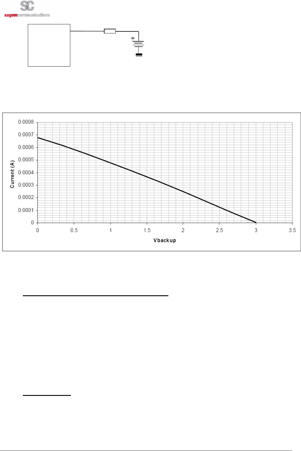
3.9.3 Charge by internal HiloNC charging function
The charging function is available on the HiloNC without any additional external power supply (the charging
power supply is provided by the HiloNC).
Charge of the back-up battery occurs only when main power supply VBAT is provided.
The recommended schematic is given hereafter:
page 21/35
Note d’étude / Technical document : URD1– OTL 5665.1– 002 / 70 884 Edition 03
Document Sagem Communications Reproduction et divulgation interdites
Sagem Communications document. Reproduction and disclosure prohibited
Figure 17: Backup battery internally charged
The resistor R depends on the charging current value provided by the battery manufacturer.
The charging curve which is done by the HiloNC is given hereafter:
Figure 18: Charging curve of backup battery
3.9.4 Backup Battery technology recommended
3.9.4.1 Manganese Silicon Lithium-Ion rechargeable Battery
Sagem Communications does not recommend using this kind of technology because of the following drawbacks:
• The maximum discharge current is limited (Shall be compliant with the module characteristics).
• The over-discharge problem: most of the Lithium Ion rechargeable batteries are not able to recover their charge when their
voltage reaches a low-level voltage. To avoid this, it is necessary to add a safety component to disconnect the
backup .battery in case of over–discharge condition. In such a case, this implementation is too complicated (too much
components for that function).
• The charging current has to be regulated.
Sagem Communications does not recommend using this kind of backup battery technology.
3.9.4.2 Capacitor battery
These kinds of backup battery have not the drawbacks of the Lithium Ion rechargeable battery.
As there are only capacitors:
• The maximum discharge current is generally bigger,
• There is no problem of over-discharge: the capacitor is able to recover its full charge even if its voltage has
previously fallen to 0V.
• There is no need to regulate the charging current.
VBACKUP
HiloNC
R
page 22/35
Note d’étude / Technical document : URD1– OTL 5665.1– 002 / 70 884 Edition 03
Document Sagem Communications Reproduction et divulgation interdites
Sagem Communications document. Reproduction and disclosure prohibited
Moreover, this kind of battery is available in the same kind of package than the Lithium Ion cell and fully
compatible on a mechanical point of view. The only disadvantage is that the capacity of this kind of battery is
significantly smaller than Manganese Silicon Lithium Ion battery. But for this kind of use (supply internal RTC
when the main battery is removed), the capacity is generally enough.
Sagem Communications strongly recommends using this kind of backup battery technology.
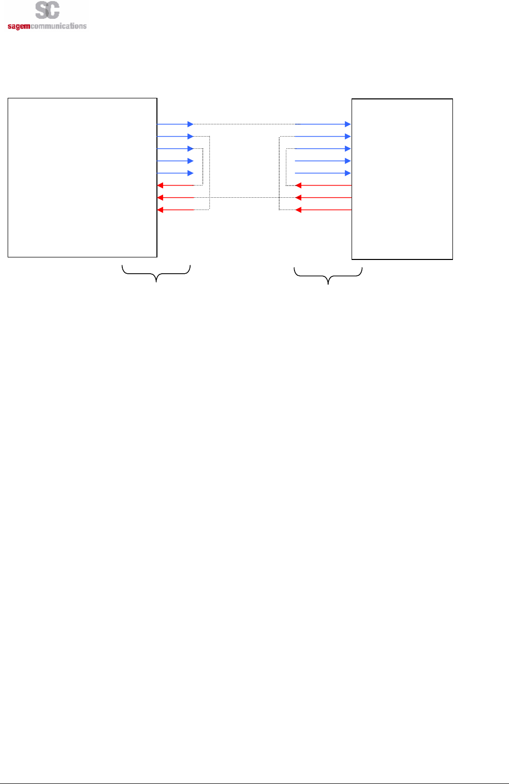
3.10 HARDWARE POWER MANAGEMENT AND MULTIPLEXING INTERFACES
In case hardware power management and multiplexing are used, it is necessary to isolate host and HiloNC
module in order not to generate current re-injection when HiloNC is switched-off.
Typical schematic (only useful signals are represented):
Figure 19: Hardware interface between HiloNC and host
In general, solution1 is enough to protect HiloNC module.
3.11 STARTING THE MODULE
First power up VBAT, which must be in the range 3.2V – 4.5V, and able to provide 2.2A during the TX bursts
(Refer to the module specification for more details).
To start the module, a low level pulse must be sent on POK_IN during 1 s minimum (at 25°C).
After a few seconds, the module puts in active state CTS when it is ready to receive AT commands.
3.12 MODULE RESET
To reset the module, a low level pulse must be sent on RESET pad during 10 ms.
3.13 MODULE SWITCH OFF
AT command “AT*PSCPOF” allows to switch off the module.
3.14 SLEEP MODE MANAGEMENT
AT command “AT+KSLEEP” allows to configure the sleep mode.
DTR, RTS, RXD
DCD, DSR, CTS, TXD, RI
Tri-state command
Buffer
HiloNC
Host
Solution 1
Solution 2
VGPIO

page 23/35
Note d’étude / Technical document : URD1– OTL 5665.1– 002 / 70 884 Edition 03
Document Sagem Communications Reproduction et divulgation interdites
Sagem Communications document. Reproduction and disclosure prohibited
When AT+KSLEEP=1 is configured :
• the HiloNC module decides by itself when it enters in sleep mode (no more task running).
• “0x00” character on serial link wakes up the HiloNC module.
When AT+KSLEEP=0 is configured :
• the HiloNC module is active when DTR signal is active (low electrical level).
• when DTR is deactivated (high electrical level), the HiloNC module enters in sleep mode after a while.
• on DTR activation (low electrical level), the HiloNC module wakes up.

page 24/35
Note d’étude / Technical document : URD1– OTL 5665.1– 002 / 70 884 Edition 03
Document Sagem Communications Reproduction et divulgation interdites
Sagem Communications document. Reproduction and disclosure prohibited
4. MANDATORY POINTS FOR THE FINAL TESTS AND TUNING
The design of the customer’s board (on which the module is soldered) must provide an access to following
signals when the final product will be completely integrated.
To upgrade the module software, Sagem Communications recommends providing a direct access to the
module serial link through an external connector or any mechanism allowing the upgrade of the module
without opening the whole product.
Serial link:
TXD Output
UART transmit
RXD Input UART receive
To debug the module software, Sagem Communications recommends providing a direct access to the
module debug port SPI (5 I/Os) through internal test points (TP) located on the customer's main board.
5. ESD & EMC RECOMMENDATIONS
5.1 HILONC ALONE
The HiloNC module alone can hold 2KV on each of the 51 pads including the RF pad.
5.2 CUSTOMER’S PRODUCT WITH HILONC
If customer’s design must stand more than 2kV on electrostatic discharge, following recommendation must be
taken into account.
5.2.1 Analysis
ESD current can penetrate inside the device via the typical following components:
• SIM connector
• Microphone
• Speaker
• Battery / data connector
• All pieces with conductive paint (plastron, special keys, etc...)
In order to avoid ESD issues, efforts shall be done to decrease the level of ESD current on electronic
components located inside the device (customer’s board, input of the HiloNC module, etc…)
5.2.2 Recommendations to avoid ESD issues
Insure good ground connections of the HiloNC module to the customer’s board.
Flex (if any) shall be shielded and FPC connectors shall be correctly grounded at each extremity.
Put capacitor 100nF on battery (not on charger), or better put varistor or ESD diode in parallel on battery
and charger wires and on all wires on bottom connector.
Uncouple microphone and speaker by putting capacitor or varistor in parallel of each wire of these devices.
page 25/35
Note d’étude / Technical document : URD1– OTL 5665.1– 002 / 70 884 Edition 03
Document Sagem Communications Reproduction et divulgation interdites
Sagem Communications document. Reproduction and disclosure prohibited
6. RADIO INTEGRATION
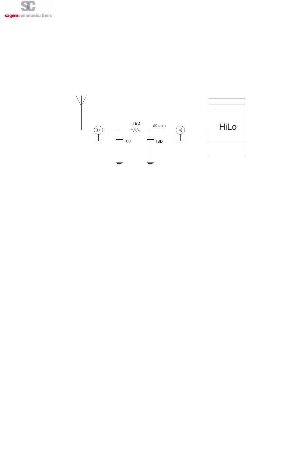
6.1 ANTENNA
- Antenna contact
• 50Ω line matching (between module and customer’s board, and with RF test point)
Figure 20: Antenna connection
Keep matching circuit on customer’s board but with direct connection in the first step – it could be
necessary to make some adjustment later, during RF qualification stage.
The selected antenna must comply with FCC RF exposure limits in GSM850 and PCS1900 band :
- GSM850 : MPE < 0.55mW/cm2 (Distance is 20 cm)
- PCS1900 : ERP < 3W
6.2 GROUND LINK AREA
Sagem Communications emphasizes the fact that a good ground contact is needed between the module and the
customer’s board to have the best radio performances (spurious, sensitivity…).
All HiloNC GND pads must be connected to the GND of the customer’s board.
6.3 LAYOUT
Warning : Isolate RF line and antenna from others bus or signals
No signals on 50 ohms area and if that is not possible, add ground shielding using different layers.
Do not add any ground layer under the antenna contact area.
Be careful on the position of the network LED (sometimes situated in front of the antenna pad ...)
Do not put any via and lines on all the forbidden area under the module, shown as the grey area on the
figure below.
Varnish must be present on all the grey area (expect solder pads) to isolate HiloNC module from the
customer’s board.
page 26/35
Note d’étude / Technical document : URD1– OTL 5665.1– 002 / 70 884 Edition 03
Document Sagem Communications Reproduction et divulgation interdites
Sagem Communications document. Reproduction and disclosure prohibited
Figure 21: Forbidden area for via and lines
6.4 MECHANICAL SURROUNDING
Avoid any metallic part around the antenna area
Keep jacks, FPCs and battery contact far from antenna area (FLEX)
FPC has to be a shielded one
6.5 OTHER RECOMMENDATIONS – TESTS FOR PRODUCTION/DESIGN
Sagem Communications guarantees the RF performances in conductive mode but strongly recommends
making RF measurements in an anechoic chamber in radiated mode (tests conditions for FTA): the radiated
performances strongly depend on radio integration (layout, antenna, matching circuit, ground area…..)
7. AUDIO INTEGRATION
Audio mandatory tests for FTA are in handset mode only so a particular care must be brought to the design of
audio (mechanical integration, gasket, electronic) in this mode.
The audio norms which describe the audio tests are 3GPP TS 26.131 & 3GPP TS 26.132.
Please note that acoustic competences are mandatory to get accurate audio performance on customer’s
product.
7.1 MECHANICAL INTEGRATION AND ACOUSTICS
Particular care to Handset Mode: FTA

page 27/35
Note d’étude / Technical document : URD1– OTL 5665.1– 002 / 70 884 Edition 03
Document Sagem Communications Reproduction et divulgation interdites
Sagem Communications document. Reproduction and disclosure prohibited
To get a better audio output design (speaker part) :
The speaker must be completely sealed on front side.
The front aperture must be compliant with speaker supplier’s specifications
The back volume must be completely sealed.
The sealed back volume must be compliant with speaker supplier’s specifications
Take care of the design of the speaker gasket (elastomer).
Foresee a stable and large enough area for the gasket of the artificial ear.
To get a better audio input design (microphone part) :
Take care of the design of the microphone (elastomer).
All receivers must be completely sealed on front side.
Microphone sensitivity depends on the shape of the device eg. about –40 ±3 dBV/Pa for clamshell.
Promote the use of pre-amplified microphone. If needed, use a pre-amplification stage.
As audio input and ouput are strongly linked :
Place the microphone and the speaker as far as possible from one another.
7.2 ELECTRONICS AND LAYOUT
Avoid Distortion & Burst noise
Audio signals must be symmetric (same components on each path).
Differential signals must be routed parallel.
Audio layer must be surrounded by 2 ground layers.
The link from one component to the ground must be as short as possible.
If possible separate the PCB of the microphone and the one of the speaker.
Reduce as much as possible the number of electronics components (loss of quality, more dispersion).
Audio tracks must be larger than 0.5 mm.

page 28/35
Note d’étude / Technical document : URD1– OTL 5665.1– 002 / 70 884 Edition 03
Document Sagem Communications Reproduction et divulgation interdites
Sagem Communications document. Reproduction and disclosure prohibited
8. RECOMMENDATIONS ON LAYOUT OF CUSTOMER’S BOARD
8.1 GENERAL RECOMMENDATIONS ON LAYOUT
There are many different types of signals in the module which are disturbing each other. Particularly, Audio
signals are very sensitive to external signals as VBAT(1).... Therefore it is very important to respect some rules to
avoid disruptions or abnormal behaviour.
8.1.1 Ground
A ground plane as complete as possible
Ground of components has to be connected to the ground layer through many vias not regularly distributed.
Top and bottom layer shall have as much as possible of ground planes.
8.1.2 Power supplies
Plan for power supply signals (VBAT, VGPIO), no loop.
Suitable power supply (VBAT, VGPIO) track width, thickness.
8.1.3 Clocks
Clock signals must be shielded between two grounds plans and bordered with ground vias.
8.1.4 Data bus and other signals
Data bus and commands have to be routed on the same plane, none of the lines of the bus shall be
parallel to other lines
Lines crossing shall be perpendicular
Suitable other signals track width, thickness.
Data bus must be protected by upper and lower ground plans
8.1.5 Radio
Provide a 50 Ohm microstrip line for antenna connection
8.1.6 Audio (see also § 10.2)
Differential signals have to be routed together, parallel (for example HSET_OUT_P/HSET_OUT_N).
Audio signals have to be isolated, by pair, from all the other signals (ground all around each pair).
Cancel any loops between VBAT and GND next to the speaker to avoid the TDMA burst noise in the
speaker during a communication.
The single-end audio signal should be adopted the same rules as differential signals.
page 29/35
Note d’étude / Technical document : URD1– OTL 5665.1– 002 / 70 884 Edition 03
Document Sagem Communications Reproduction et divulgation interdites
Sagem Communications document. Reproduction and disclosure prohibited
Figure 22: Layout of audio differential signals on a layer n
Figure 23: Adjacent layers of audio differential signals
(1). Warning: Magnetic field generated by VBAT tracks may disturb the speaker, causing audio burst noise. In
this case, one shall modify routing of the VBAT tracks to reduce the phenomena.
8.2 EXAMPLE OF LAYOUT FOR CUSTOMER’S BOARD
The figure Figure 24 shows an example of layer allocation for a 6 layers circuit (for reference only):
Figure 24: layer allocation for a 6 layers circuit
9. RECOMMANDATIONS FOR CUSTOMER INDUSTRIALIZATION
Please note for following chapters that except where standards are indicated, the given characteristics should be
considered as validated conditions used on Sagem Communication product.
Other conditions depending of the customer’s factory process are not validated but can be submitted to
Sagem Communication for proficiency.
9.1 MOISTURE LEVEL
According to IPC/JEDEC J-STD 20, the HiloNC has the following MSL level : 3 (Targeted).
Layer n-1
Layer n
Layer n+1
GND
HSET_OUT_P
GND
GND
HSET_OUT_P
GND
HSET_OUT_N
Layer 1: Components (HiloNC)
Layer 2: Bus
Layer 3: Power supply
Layer 4: Complete GND layer
Layer 5: Audio, clocks, sensitive signals
Layer 6: GND,test points

page 30/35
Note d’étude / Technical document : URD1– OTL 5665.1– 002 / 70 884 Edition 03
Document Sagem Communications Reproduction et divulgation interdites
Sagem Communications document. Reproduction and disclosure prohibited
Soak requirements Level
Floor Life
Standard Accelerated Equivalent
Time Conditions Time (hours) Conditions Time (hours) Conditions
3 168 hours
<= 30°C/60% RH
192 +5/-0 30°C / 60% RH
40 +1/-0 60°C / 60%RH
It means that the customer’s factory must process and solder the HiloNC on the customer’s board at least 168
hours (7 days) after the HiloNC sealed package have been opened. This duration is given for factory floor
conditions of T°<30°C, HR 60%.
If this duration can not be fulfilled, the HiloNC part must be baked again.
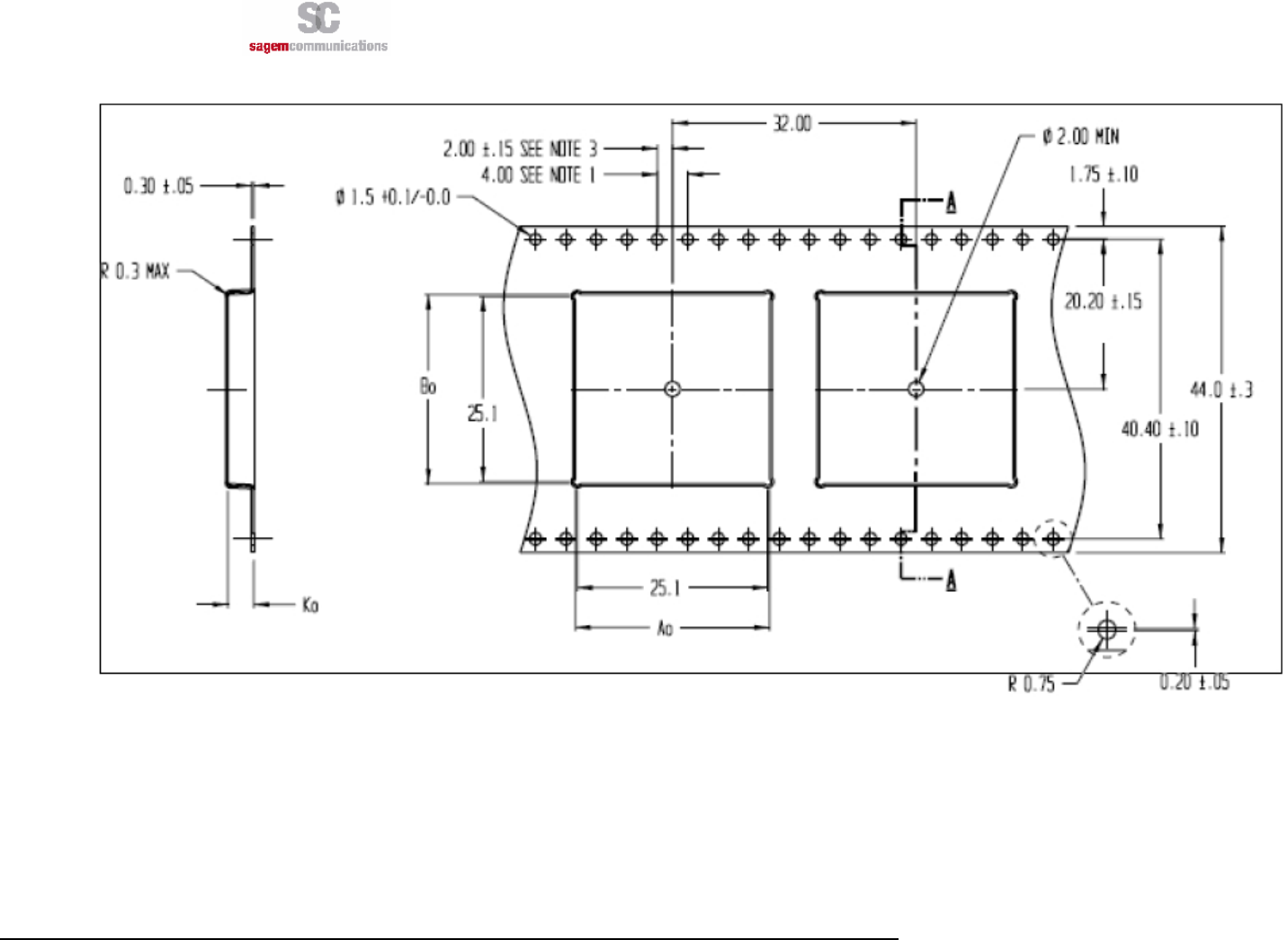
9.2 PACKAGE
The HiloNC module is delivered in Tape and Reel package which is hermetically sealed to prevent from moisture
and ESD.
The characteristics of the T&R are given in the drawing below.
page 31/35
Note d’étude / Technical document : URD1– OTL 5665.1– 002 / 70 884 Edition 03
Document Sagem Communications Reproduction et divulgation interdites
Sagem Communications document. Reproduction and disclosure prohibited
page 32/35
Note d’étude / Technical document : URD1– OTL 5665.1– 002 / 70 884 Edition 03
Document Sagem Communications Reproduction et divulgation interdites
Sagem Communications document. Reproduction and disclosure prohibited
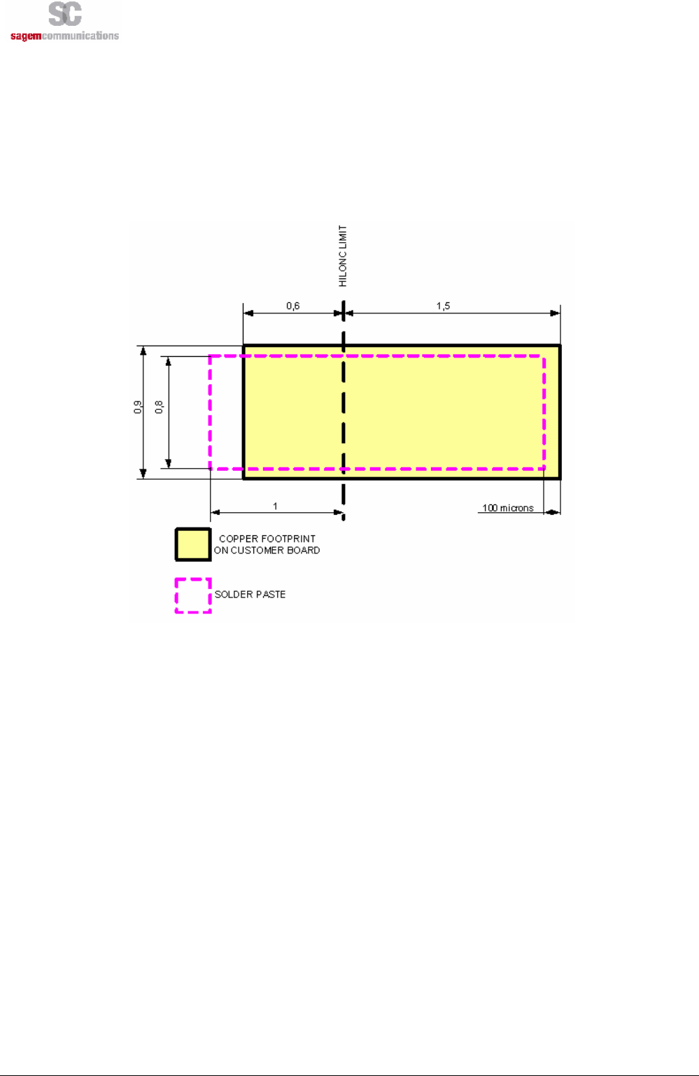
9.3 SOLDER MASK
Below are given soldering characteristics to report the HiloNC on the customer’s board.
Copper footprint is shown in yellow on the figure below. Solder mask footprint is shown in pink.
Please note that copper mask and solder mask do not strictly recover themselves.
Figure 25 : Solder mask design
9.4 SOLDER PASTE
Solder paste : M705-GRN360-K-V (Senju Metal Industry Co., Ltd.)
Alloy composition : Sn96.5-Ag3.0-Cu0.5
Melting temperature : solidus 216°C / Peak 217°C / liquidus 220°C
Sagem Communication recommends a stencil thickness of 135 µm.
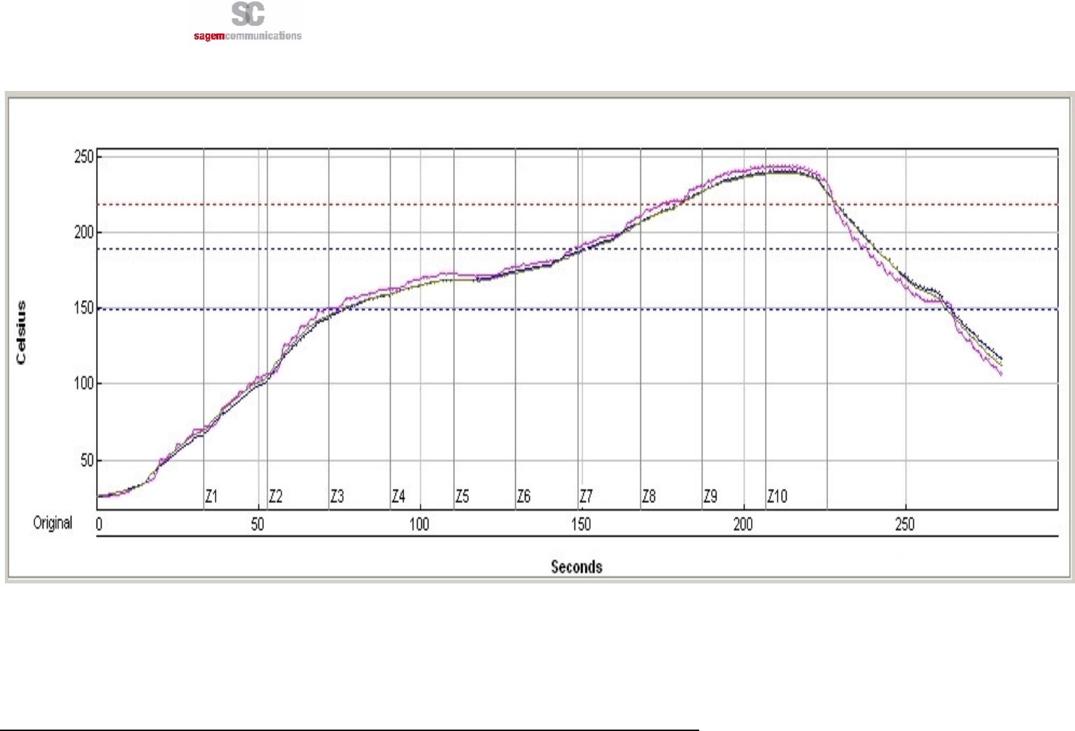
9.5 PROFILE FOR REFLOW SOLDERING
A convection type soldering oven is recommended.
Typical usable profile is shown on the next figure. The final profile has to be tuned depending on other elements
like solder paste, customer’s board, other components,…
Peak temperature : 245°C
Average ramp up rate : 3°C/second max
Average ramp down rate : TBC
page 33/35
Note d’étude / Technical document : URD1– OTL 5665.1– 002 / 70 884 Edition 03
Document Sagem Communications Reproduction et divulgation interdites
Sagem Communications document. Reproduction and disclosure prohibited
Figure 26 : Typical thermal profile
The HiloNC module is a Lead-free product which has been validated integrated in a lead-free product, using a lead-free factory process.
No test has been performed using a leaded process. Sagem Communication does not recommend to use a factory leaded process and does not guarantee any
reliable result on the final product.
page 34/35
Note d’étude / Technical document : URD1– OTL 5665.1– 002 / 70 884 Edition 03
Document Sagem Communications Reproduction et divulgation interdites
Sagem Communications document. Reproduction and disclosure prohibited
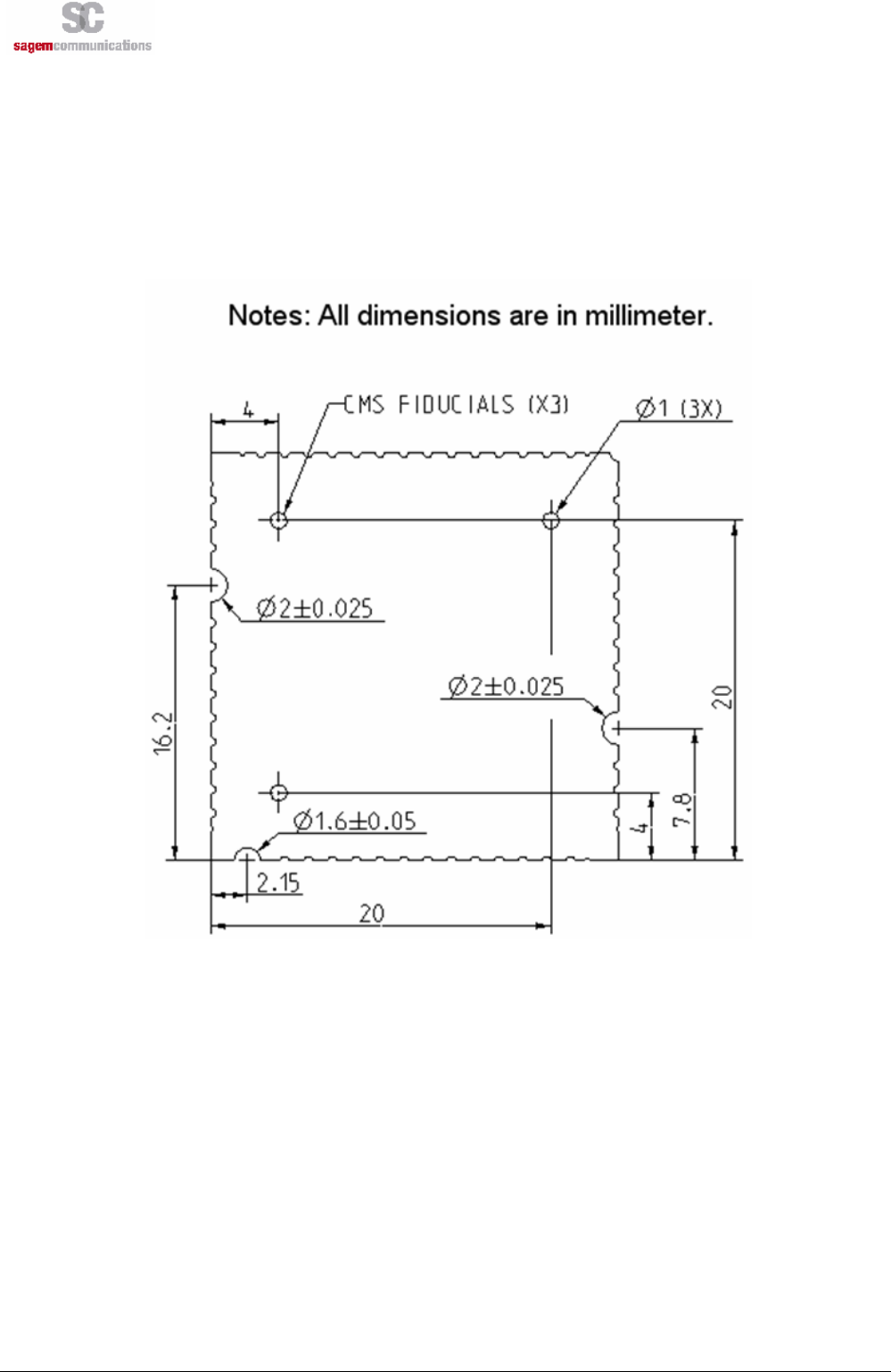
9.6 SMT MACHINE
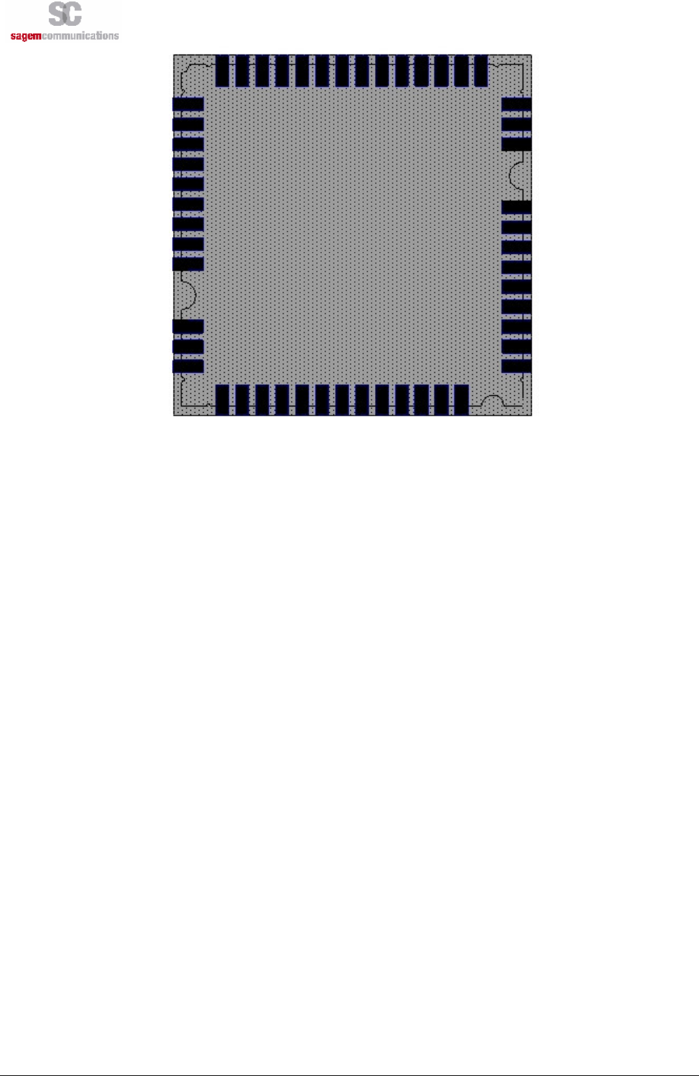
HiloNC is optimized for use with pick-and-place machines.Optical inspection for placement is possible with SMD
fiducials placed on the bottom side of the HiloNC. SMD fiducials are not symmetrical in order to help optical
inspection to define the right orientation.
Figure 27 : CMS fiducials positions
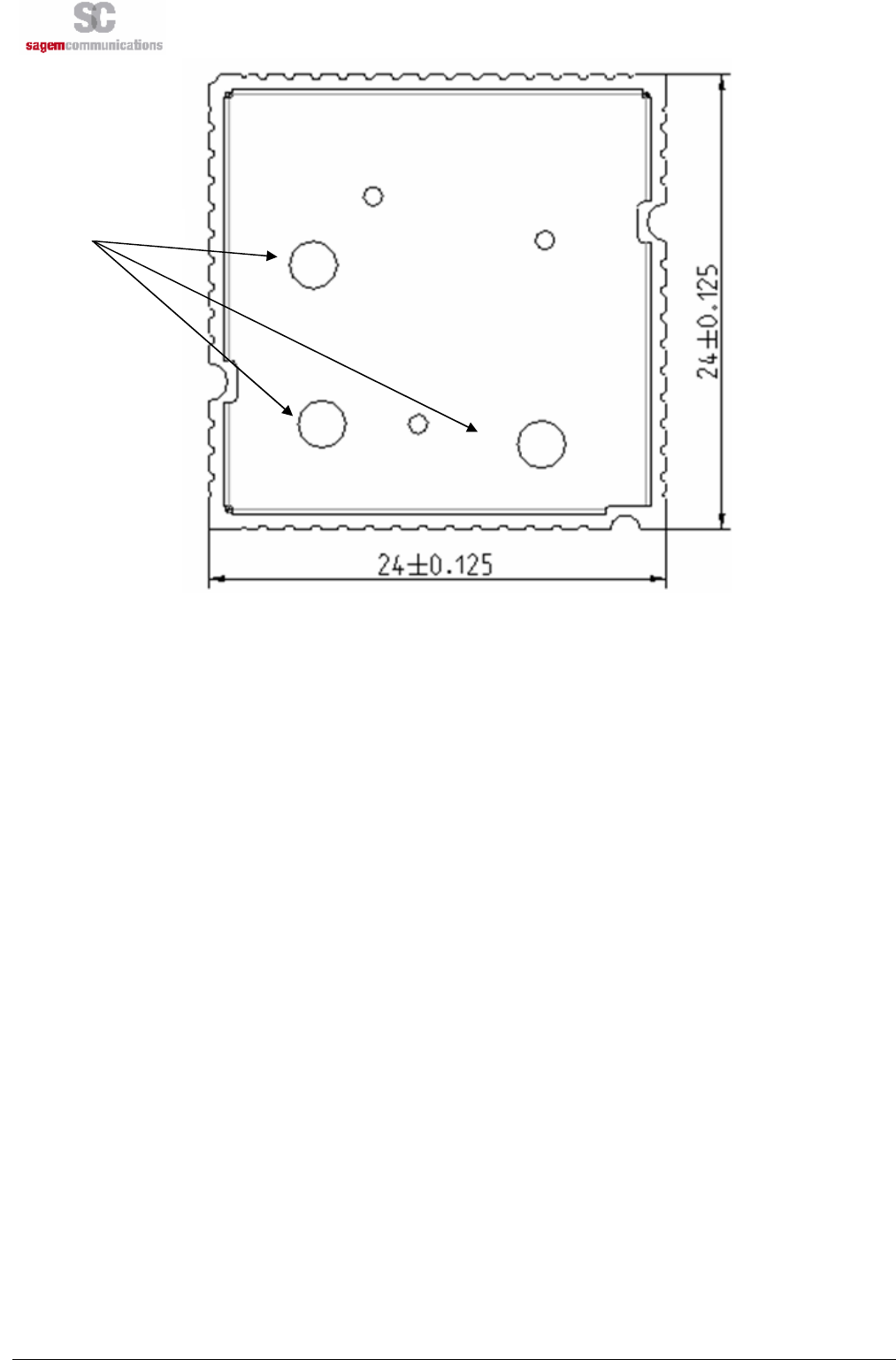
9.7 UNDERFILL
Despite its important reliability, some customer could request for some specific and extreme applications the
underfill of onboard components.
The HiloNC’s shield has be designed accordingly to allow this process, as shown in the figure below.
More details will be given in a specific application note.
page 35/35
Note d’étude / Technical document : URD1– OTL 5665.1– 002 / 70 884 Edition 03
Document Sagem Communications Reproduction et divulgation interdites
Sagem Communications document. Reproduction and disclosure prohibited
Figure 28 : Underfill holes
9.8 SECOND REFLOW SOLDERING
Even if Sagem Communications recommends a single reflow soldering, a second reflow soldering can be
conceivable (only if underfill has not been already performed). Positive tests have been performed with HiloNC
on the bottom side.
Second reflow soldering is not possible if HiloNC module has been already underfilled.
9.9 HAND SOLDERING
Hand soldering is possible.
An especial care must be considered to properly position the HiloNC on its copper footprint during hand
soldering. Begin with pads diagonally opposite to help in proper positioning.
9.10 REWORK
Rework is possible, for repair purpose for example.
An especial care must be considered in order not to overheat the HiloNC.
10. LABEL
The HiloNC module is labelled with its own FCC ID(VW3HILONC) on its bottom side. When the module is
installed in customer’s product, the FCC ID label on the module will not be visible. To avoid this case, an exterior
label must be stuck on the surface of customer’s product signally to indicate the FCC ID of the enclosed module.
This label can use wording such as the following: “Contains Transmitter module FCC ID: VW3HILONC” or
“Contains FCC ID: VW3HILONC”.
Underfill Holes