SEBINE Technology W210A REMOTE CONTROL/SECURITY DEVICE TRANSCEIVER User Manual
SEBINE Technology, Inc. REMOTE CONTROL/SECURITY DEVICE TRANSCEIVER Users Manual
Users Manual

W210A
W210A_20110725.hwp 1
WDAS
Wireless Data Acquisition and Control System
W210A
User's Manual
Ver 2.0
SEBINE Technology, Inc.

W210A
W210A_20110725.hwp 2
This device complies with Part 15 of the FCC Rules. Operation is subject to the following
two conditions: (1) This device may not cause harmful interference, and (2) this device must
accept any interference received, including interference that may cause undesired operation.

W210A
W210A_20110725.hwp 3
CONTENTS
1. Summary
1.1 Product Introduction
1.2 Specification
2. Operation
2.1 PC MODE
3. Device Connection
3.1 Power Supply
3.2 Analog Input Connection
4. Environment Setup
4.1 Hardware Connection
4.2 Setup List of Each Mode
5. Examples
Appendix 1. Dimension
Appendix 2. R&TTE
Appendix 3. Document Information
W210A
W210A_20110725.hwp 4
1. Summary
1.1 Product Introduction
W210A is one of WDAS(Wireless Data Acquisition and Control System) products
and it is a wireless data transmitter-receiver which receives analog input data for
controlling signal by using 433MHz RF frequency bandwidth. W210A allows users
to set communication channels via environment setting. Usable frequency number,
channel number, and serial number are printed in shipping products.
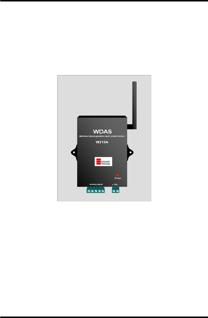
Figure 1. W210A

W210A
W210A_20110725.hwp 5
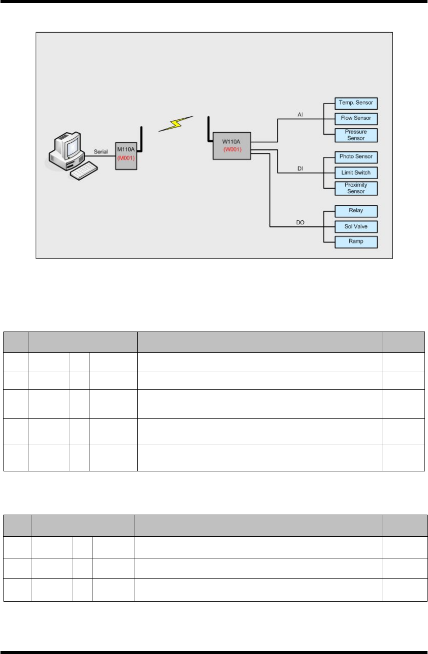
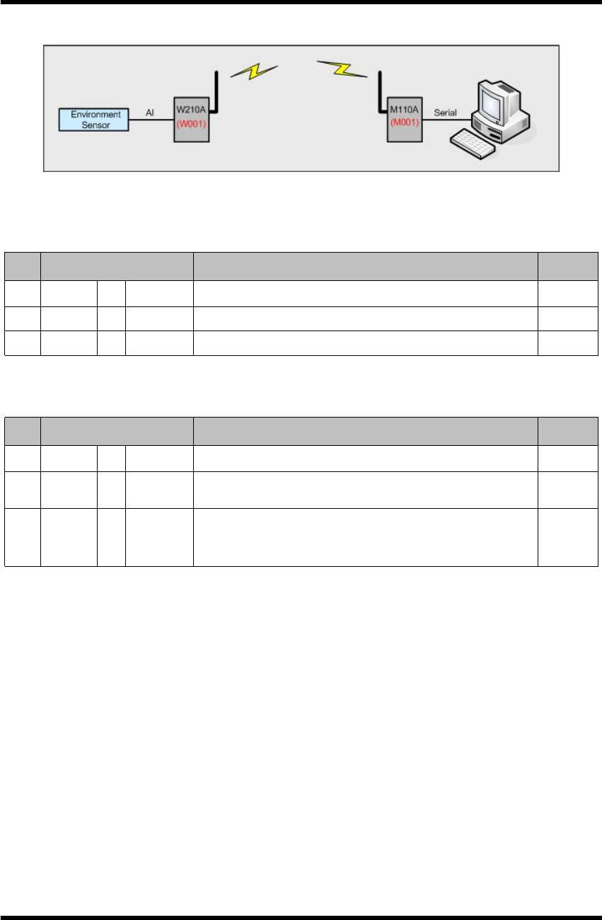
1.1.1 Application examples
Figure 2. On/Off Status Wireless Transmission by W210A and M110A
1.1.2 Product usage
lCable system replacement : Maintenance difficulty with cables is solved
lHard environment for cable installation : Environment that requires long and co
mplicated cable installation is solved
lUneasy area for data acquisition by cable : Outdoor tank monitoring system
1.1.3 Product application area
lPump, pipeline, liquid flow monitoring system
lTank level, temperature monitoring system
1.1.4 Product parts
W210A main body, one λ/4 dipole antenna, one power connector, one Analog
Input connector

W210A
W210A_20110725.hwp 6
Item Specification
Name W210A
Dimension 109mm(L)×85mm(W)×18.6mm(H) (w/o Antenna)
Housing Aluminum
Weight 150g (w/o Antenna)
Power Supply +12Vdc ±10%, Reverse Power/Overvoltage/Overcurrent Protection
Current
Consumption Rx 80mA Tx 86mA WDT Reset 88mA (@12Vdc)
Operating
Temperature -10℃ ~ +60℃
RF Features
• Frequency : 433.0625MHz ~ 434.7625MHz
• Channel Spacing : 25KHz
• Transmitter Power : 73dBuV/m
• Receiver Sensitivity : -116 ~ -120dBm(-116dBm typ.)
• Modulation : FSK
• Bandwidth : < 14KHz
Performance
• Expected Line-Of-Sight Range :
Up To 1.5km with λ/4 Dipole Antenna
• RF Data Rate :
4.8K Baud, 7.2K Baud
I/O
Interface
Analog
Input
2Ch. Analog Input, with 16Bit Resolution
(0~5V, 0~10V, 4~20mA)
User Selectable Input Type : Current or Voltage
User Selectable Input Voltage Range : 0~5V or 0~10V
Antenna
Interface
• SMA(Female, Reverse)Connector
• Impedance 50Ω
1.2 Specification
Table 1. W210A Specification
W210A
W210A_20110725.hwp 7
2. Operation
W210A can use only PC MODE. Refer the Programmer guide for detailed protocol
and Function Code.
2.1 PC MODE
2.1.1 Definition of PC MODE
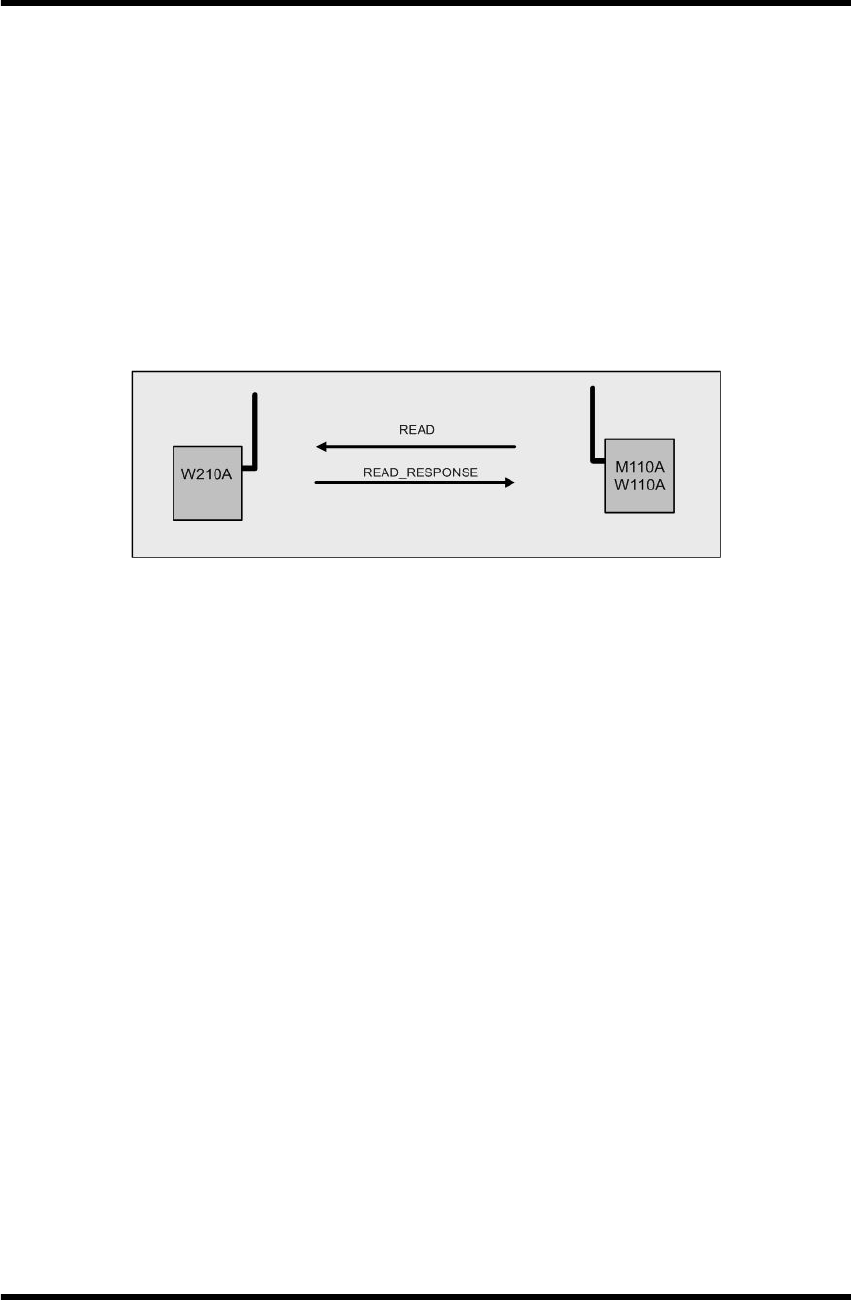
Through M110A(PC MODE), W110A(Only PC MODE) with serial port, W210A
execute the command when valid Function Code is received.
- Valid receiver Function Code : READ
Figure 3. PC MODE of W210A
2.1.2 Function Code available at PC MODE
- READ : Through M110A(PC MODE), W110A(Only PC MODE) with serial port,
current analog input status is read when W210A receives Function Code of
inquiry of analog input status.
- READ_RESPONSE : Function Code of READ_RESPONSE is used when READ
Function Code is received and current analog input status is transmitted.
2.1.3 Environment setting list before PC MODE use
- Non
W210A
W210A_20110725.hwp 8
3. Device Connection
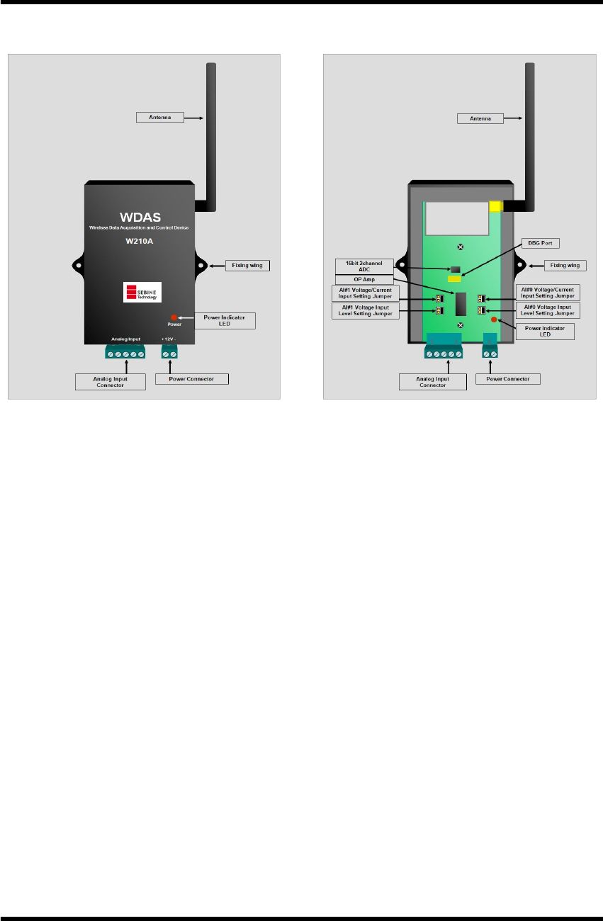
Figure 5. W210A Outer Figure 6. W210A Inner
W210A
W210A_20110725.hwp 9
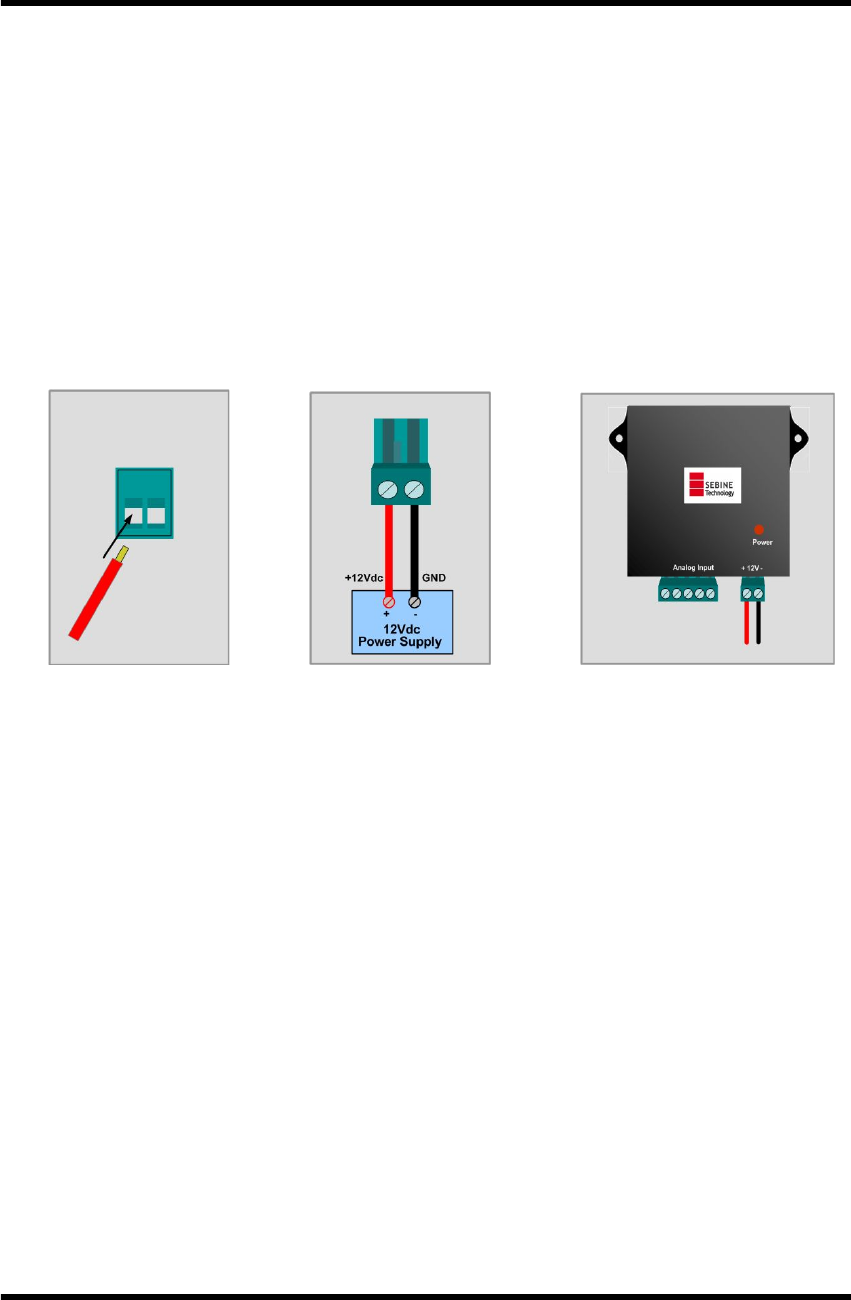
3.1 Power Supply
W210A works at +12Vdc and equipped with Reverse Power / Overvoltage /
Overcurrent Protection circuitry. Power is supplied by power connector provided
at product purchase as shown in figure below. W210A has no external power
switch and it becomes in working mode when the power is supplied. If normal
power is supplied, power supply indicator LED is on.
As shown in Figure 7, remove the skin of wire about 7mm and put it into the
terminal and tighten it by turning the left screw using screwdriver.
As shown in Figure 8, connect it to power.
As shown in Figure 9, connect the terminal to power port of W210A, Make
sure the direction is exact as shown in Figure 9.
Figure7. Power Supply-1 Figure8. Power Supply-2 Figure9. Power Supply-3
※ Notice
Readily accessible disconnect device shall be incorporated external to the
equipment.
W210A
W210A_20110725.hwp 10
3.2 Analog Input Connection and Setting
W210A supports 2 input channel. For analog input function, use Analog Input
connector in Figure 10. Analog Input connector is included in product purchase.
Connection method is same as power supply connection method.
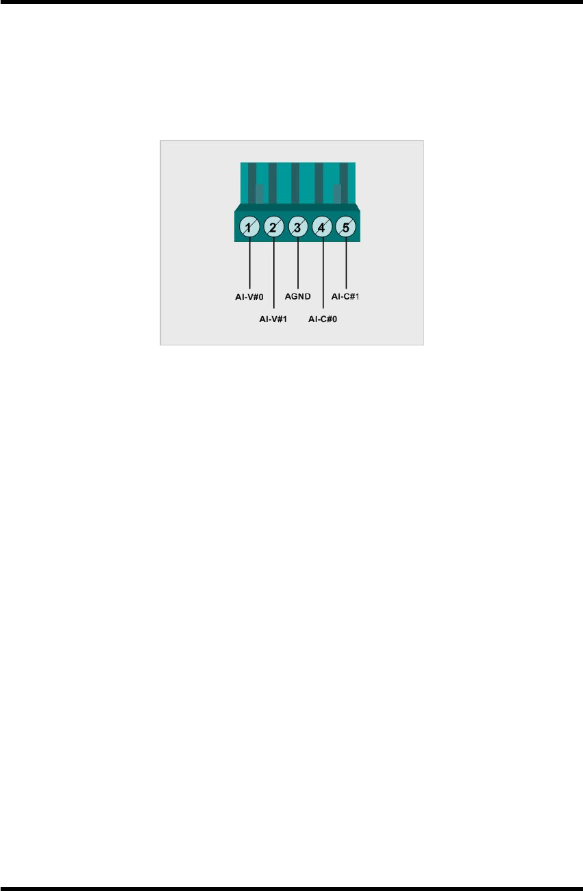
Figure 10. W210A connector
3.2.1 Analog input connection
Analog input channel generates input via the difference between AGND and
corresponding analog input channel pins. Thus, the both ends of device that
generates analog input should be connected to corresponding channel pins and
AGND.
3.2.2 Analog input channel setup
For use of anlog input, AI#0 voltage input level setting jumper, AI#1 voltage
input level setting jumper, AI#0 voltage/current input setting jumper, AI#1
voltage/current input setting jumper adjustments are needed as shown in Figure
11.
W210A
W210A_20110725.hwp 11
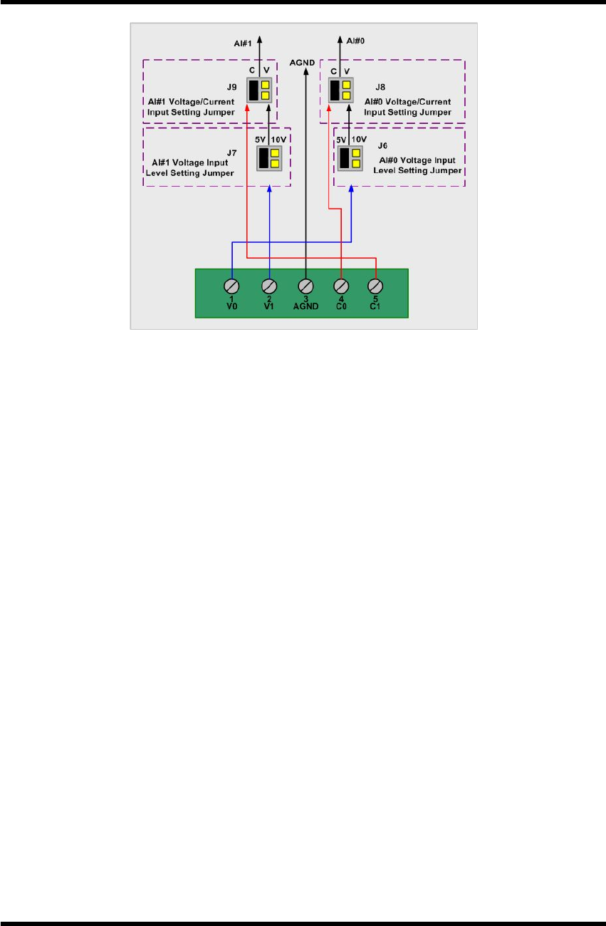
Figure 11. W210A analog input channel setting concept
AI#0 : AI#0 can select voltage/current input receipt. When receiving voltage, set
the jumper of J8 as V and adjust the voltage input range, then receive voltage via
pin 1 of Analog Input connector. When receiving current, set the jumper of J6 as
C, then receive current via pin 4 of analog input connector.
AI#1 : AI#1 can select voltage/current input receipt. When receiving voltage, set
the jumper of J9 as V and adjust the voltage input range, then receive voltage via
pin 2 of Analog Input connector. When receiving current, set the jumper of J9 as
C, then receive current via pin 5 of analog input connector.
W210A
W210A_20110725.hwp 12
4. Environment setup
Environment setup can be made through SetModemEnv.exe program. For details,
consult the corresponding manual.
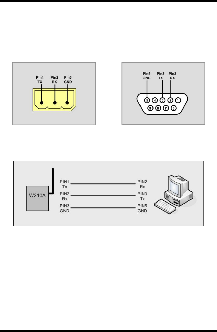
4.1 Hardware connection
Use DBG port for PC connection shown in Figure 13.
Figure 13. Hardware connection-1(W210A) Figure 14. Hardware connection-2(PC)
For communication frequency adjustment, port and PC must be connected via
serial communication program as shown in Figure 13.
Figure 15. Hardware connection-3
The hardware connection between W210A and PC can be done as shown in
Figure 15.
W210A
W210A_20110725.hwp 13
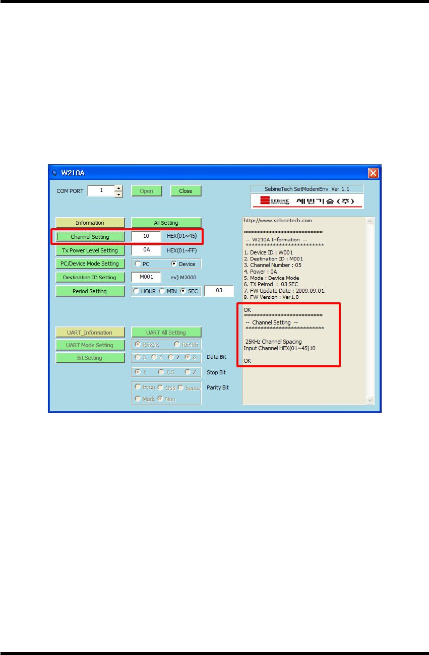
4.2 Setup list of each mode
4.2.1 PC MODE
- PC/DEVICE MODE Setting : PC MODE Setting
- Channel Setting : Communication Frequency Setting
- Tx Power Level Setting : Communication RF Power Level Setting
4.2.3 Environment Setting Program
1) Channel Setting(Communication Frequency Setting)
Figure 16. Environment Setting Program-Channel Setting Setting
2) Tx Power Level Setting(Communication RF Power Level Setting)
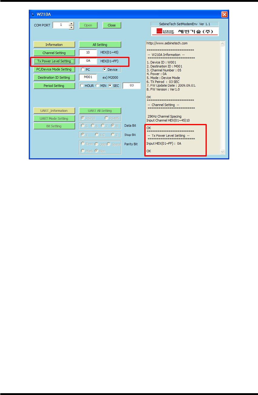
W210A
W210A_20110725.hwp 14
Figure 17. Environment Setting Program-Tx Power Level Setting

W210A
W210A_20110725.hwp 15
5. Examples
(EX 1) M110A(PC MODE) to W210A(PC MODE) Communication
Figure 21. M110A to W210A Communication Example
W210A
W210A_20110725.hwp 16
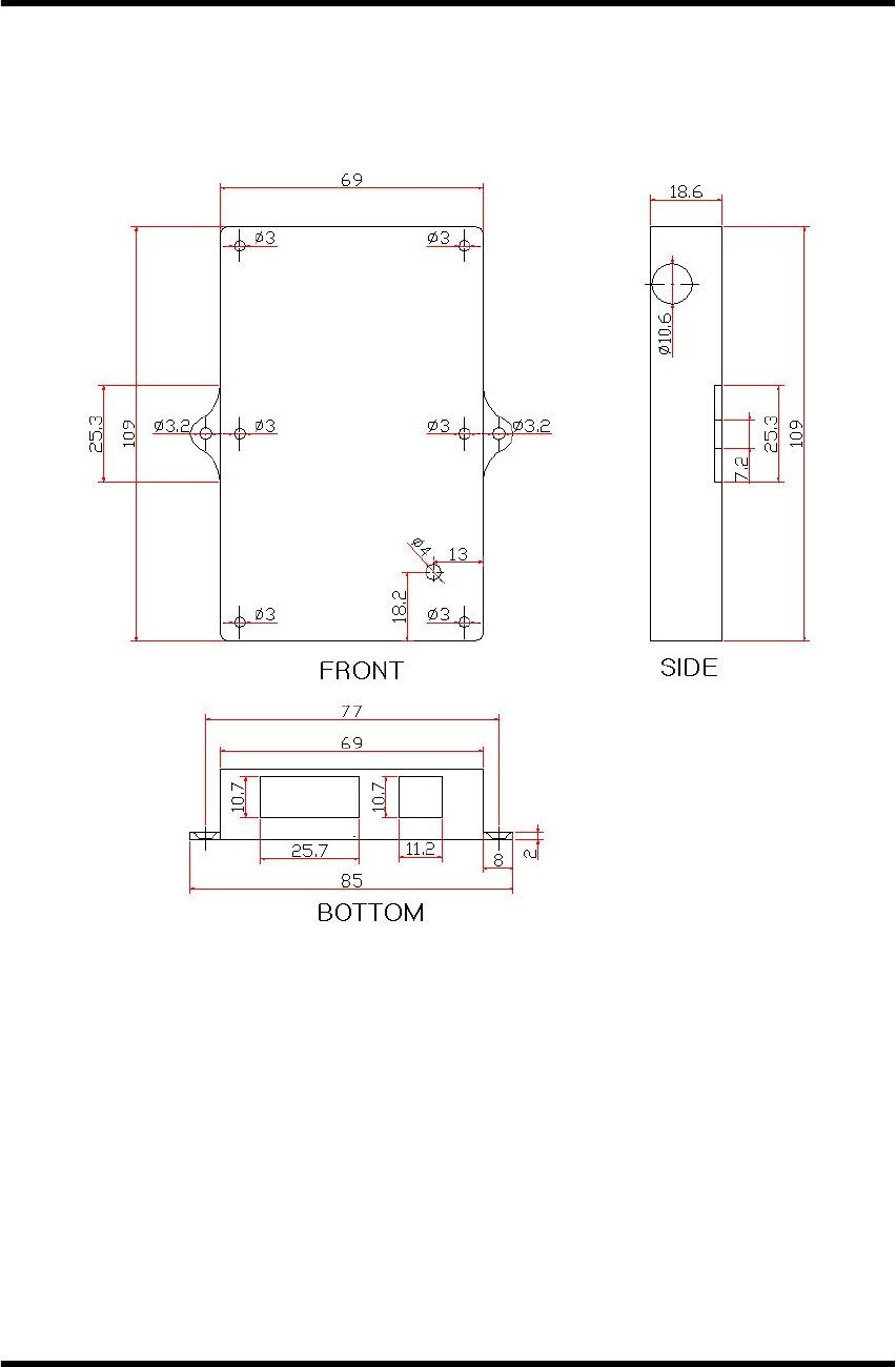
Appendix 1. Dimension

W210A
W210A_20110725.hwp 17
Appendix 2. R&TTE
Hereby, SEBINE Technology, Inc. declares that this device(M/N:W210A) is in
compliance with the essential requirements and other relevant provisions of
Directive 1999/5/EC.

W210A
W210A_20110725.hwp 18
Appendix 3. Document Information
Revision H/W Version Description
1.0 RF1-AE-AI Ver1.2 02/23/2010 - Initial Release Version
2.0 RF1-AE-AI Ver1.2 07/13/2011 - Modified

W210A
W210A_20110725.hwp 19
SEBINE Technology, Inc.
Homepage : www.sebinetech.com
E-mail : tech@sebinetech.com
RN 202, Daedeok Radio Engineering Center, 694, Tamnip-dong,
Yuseong-gu, Daejeon, Korea 305-510
Tel : 82-42-935-2084, 2085
Fax : 82-42-935-2088

Programmer's Guide_20110718_eng.hwp 1
RF MODEM / WDAS
Programmer's Guide
Ver 1.0
Ver 1.0
SEBINE Technology, Inc.

Programmer's Guide_20110718_eng.hwp 2
CONTENTS
1. Summary
2. Basic Communication Concept
3. Protocol
3.1 Protocol
3.2 Protocol and Device Operation Mode
3.3 Use of FUNCTION CODE
4. Communication Consumption Time
5. Example
Appendix 1. Document Information

Programmer's Guide_20110718_eng.hwp 3
Group Products I/O Interface
RF MODEM M110A RS232/RS485 Interface
WDAS
W110A DI 8ch, DO 8ch, AI 5ch, RS232 Interface
W210A AI 2ch
W310A DI 8ch, DO 8ch
W410A DI 4ch
W510A AO 2ch
1. Summary
RF MODEM and WDAS(Wireless Data Acquisition and Control System) is a wireless
transmitter/receiver device. RF MODEM and WDAS are distinguished depending on
I/O interface.
[Products List '09]
Table 1. Products Classification with I/O
Users select applicable products on their desired system and make a easy use
through simple environment setup and GUI.
For use of RF MODEM and WDAS, use SEBINE Technology's own environment
setup program and protocol.
M110A can't RF transmission and reception without control signal.
Programmer's Guide_20110718_eng.hwp 4
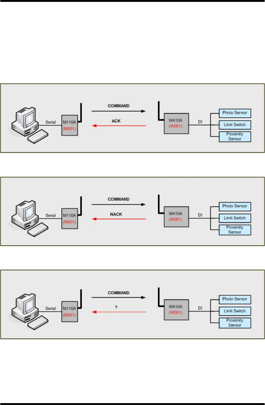
2. Basic Communication Concept
For system configuration using RF MODEM and WDAS, 1:1, 1:N method is applied.
All products receive command through RF communication and transmit ACK or
NACK for received command through RF communication. ACK means command is
done correctly and NACK means command is done incorrectly. However, if ACK or
NACK is not received within some amount of time, RF communication has problem.
So, users should always check ACK, NACK for system operation.
Figure 1. Transmission ACK after correct command receive (W410A)
Figure 2. Transmission NACK after incorrect command receive(W410A)
Figure 3. Command receive fail(W410A)

Programmer's Guide_20110718_eng.hwp 5
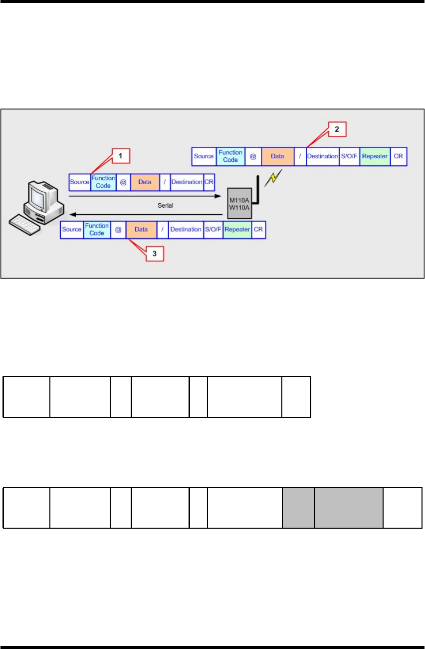
3. Protocol
3.1 Protocol
For system configuration with RF MODEM and WDAS, use SEBINE Technology's
own protocol for control of installed RF MODEM and WDAS. Protocol is as follows.
SOURCE FUNCTION
CODE @
Control
Signal
DATA
/ DESTINATION S/O/F REPEATER CR
3.1.1 SOURCE
- Description : Unique ID of Transmitter(M110A, W110A, W210A, W310A, W410A,
W510A). It is pre-fixed at factory delivery.
- Length : 4byte
- Example : RF MODEM : Mxxx -> M001
WDAS : Wxxx -> W001
3.1.2 FUNCTION CODE
- Description : Command. Use appropriate FUNCTION CODE for each component
Function
Code Command Description SOURCE DESTINATION
10 WRITE Signal output command to
DESTINATION
with AO, DO function
M110A,
W110A
W110A,
W310A,
W510A
11 WRITE_SERIAL
Data communication command to
DESTINATION with serial interface
function
M110A,
W110A
M110A,
W110A
20 READ Measure input signal command to
DESTINATION with AI, DI function
M110A,
W110A
W110A,
W210A,
W310A,
W410A
21 READ_RESPONSE Read and transmit signal command to
SOURCE with AI, DI function
W110A,
W210A,
W310A,
W410A
M110A,
W110A
22 STATUS_READ Measure output signal command to
DESTINATION with AO, DO function
M110A,
W110A
W310A,
W510A
23 STATUS_RESPONSE Reply output signal value command to
DESTINATION with AO, DO function
W 3 1 0 A ,
W510A
M110A,
W110A
Table 2. Function Code
- Description : 2byte
- Example : None

Programmer's Guide_20110718_eng.hwp 6
3.1.2 @
- Description : Classifier for beginning of DATA
※‘@’is a reserved classifier. User cannot use it for other use
- Length : 1 Byte
- Example : None
3.1.3 Control Signal DATA
- Description : Control Signal Data sent to DESTINATION by SOURCE. Depending
on products, contents of Control Signal DATA changes or skipped. In ACK, NACK,
it is skipped.
- Length : 0 ~ 50byte
- Example : None
3.1.4 /
- Description : Classifier for end of DATA
※‘/’is a reserved classifier. User cannot use it for other use
- Length : 1 Byte
- Example : None
3.1.5 DESTINATION
- Description : Object communicates with SOURCE (M110A, W110A, W210A,
W310A, W410A, W510A)
- Length : 4 Byte
- Example : RF MODEM : Mxxx -> M001
WDAS : Wxxx -> W001
3.1.6 S/O/F
- Description :Transmitting/Receiving data Status (S - Send, O - OK, F - Fail).
Automatically generated from device.
- Length : 1 Byte
- Example : None
3.1.7 REPEATER
- Description : ID of Repeater passes data sent by SOURCE. It is automatically
generated by device. If not passed through repeater, R00 is displayed.
- Length : 3 Byte
- Example : R110A : Rxx -> R01

Programmer's Guide_20110718_eng.hwp 7
3.1.8 CR
- Description : Carriage Return [ = 0x0D ]
- Length : 1 Byte
- Example : None
Programmer's Guide_20110718_eng.hwp 8
3.2 Protocol and Device Operation Mode
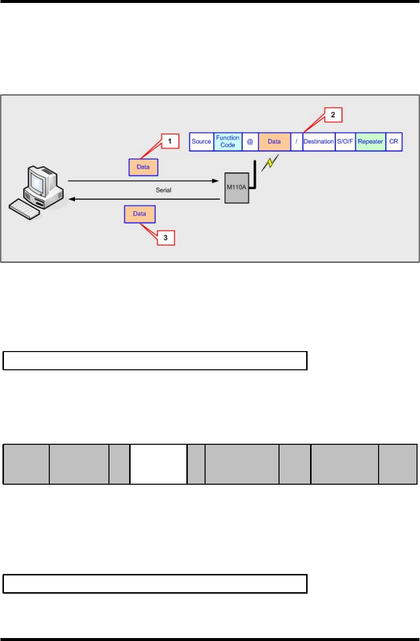
3.2.1 PC MODE of device with Serial Interface
: RF MODEM(M110A), WDAS(W110A)
If M110A, W110A(In Serial Port use, only PC MODE is available) set as PC MODE
for 1:1, 1:N system configuration, device operates as follows.
Figure 4. PC MODE of Serial Interface
1) PC->M110A(W110A)
Users transmit Device ID, FUNCTION CODE, @, Control Signal DATA, /,
DESTINATION ID of Device to be communicated, CR to M100A(W110A) through
serial communication program.
SOURCE FUNCTION
CODE @
Control
Signal
DATA
/ DESTINATION CR
2) M110A(W110A) <-> RF
M110A(W110A) automatically generate proper Status, REPEATER ID for received
data and transmit them by RF.
SOURCE FUNCTION
CODE @
Control
Signal
DATA
/ DESTINATION S/O/F REPEATER CR
Programmer's Guide_20110718_eng.hwp 9
3.2.2 DEVICE MODE of device with Serial Interface : RF MODEM(M110A)
If system is configurated by setting DEVICE MODE for M110A, 1:1, that is only RF
MODEM to RF MODEM communication configuration is possible. It operates as
follows.
Figure 5. DEVICE MODE of Serial Interface device
1) PC->M110A
Users transmit control signal data to M110A through serial communication program.
(Max 50Byte)
Control Signal DATA
2) M110A <-> RF
M110A automatically generates proper SOURCE, FUNCTION CODE, @, /, Status,
REPEATER ID, CR for received data via serial interface and transmit them via RF.
SOURCE FUNCTION
CODE @
Control
Signal
DATA
/ DESTINATION S/O/F REPEATER CR
3) M110A -> Serial Interface Controller
If DESTINATION device that request communication is RF MODEM and DEVICE
MODE is set, only Control Signal DATA part is transmitted to Serial Interface
Controller via serial port by protocol.
Control Signal DATA

Programmer's Guide_20110718_eng.hwp 10
3.2.3 PC MODE of device with DI, DO, AI, AO function : WDAS
If system is configured by setting PC MODE for WDAS, 1:1, 1:N communication
setup is available through RF MODEM(M110A), WDAS(W110A Serial Port)with Serial
Port.
Figure 6. PC MODE of DI, DO, AI, AO device
When command is received from RF MODEM(M110A), WDAS(W110A Serial Port),
perform corresponding operation for each model of WDAS, For details, refer the
application example.

Programmer's Guide_20110718_eng.hwp 11
3.3 Use of FUNCTION CODE
3.3.1 10 : WRITE
1) Description : Command that device with Serial Interface (M110A, W110A) in PC
MODE becomes SOURCE, then DESTINATION device in PC MODE with DO[Digital
Output], AO[Analog Output] function generates desired signal value.
2) Send Data :
=> DATA : *DO(2Byte)*, *AO0(4Byte)*AO1(4Byte)*
※‘*’is a classifier. It must be inserted.
=> S/O/F
▸ S : Data Send
3) Value Range of DATA
▸ DO : ※ Current applied products are W110A, W310A
Classification Digital Port
Note
Name DO#7 DO#6 DO#5 DO#4 DO#3 DO#2 DO#1 DO#0
Signal Range 0~1 0~1 0~1 0~1 0~1 0~1 0~1 0~1 1="High",
0="Low"
Data Range
(Char) 0 ~ F 0 ~ F
Description
8 DO ports in bit is expressed as
Express 0x00 ~ 0xFF(Hex) in CHAR(2Byte)
Ex) Express 0xF0(Hex) -> F0(Char)
- Example :
Data DO 1st Byte DO 2nd Byte
Note
Port No. DO#7 DO#6 DO#5 DO#4 DO#3 DO#2 DO#1 DO#0
Output Signal 1 1 1 1 1 1 1 1 1="High",
0="Low"
DO Data
Value F F
Description All DO#0 ~ DO#7 Signal Output “High"
=> DATA = *FF*

Programmer's Guide_20110718_eng.hwp 12
▸ AO : ※ Current applied product is W510A
Classification Analog Port
Note
Name AI#0 AI#1
Signal Range 0~5V, 0~10V, 0~20mA 0~5V, 0~10V, 0~20mA
Data Range
(Char) 0000~FFFF(16Bit) 0000~FFFF(16Bit)
Description
0~5V : 0V->0000, 5V->FFFF
0~10V : 0V->0000, 10V->FFFF
0~20mA : 0mA->0000, 20mA->FFFF
AO0, AO1 is generated proportionally in 16
bit
resolution (0000~FFFF(HEX)) depending on
the
setup output value range. AO Data Value is
an
approximate value.
- Example :
Classification Analog Port
Note
Port Num AI#0 AI#1
Output Signal FFFF 0000
AO Data
Value 5V when 0~5V 0V when 0~10V
Description AO Data Value is approximate value.
=> DATA = *FFFF*0000*
4) ACK Data :
=> DATA : Blank
=> S/O/F
▸ O : Data Receive OK
▸ F : Data Receive Fail
5) Applicable products :
▸ SOURCE : M110A, W110A
▸ DESTINATION : W110A , W310A, W510A
Programmer's Guide_20110718_eng.hwp 13
6) Example :
▸ M110A(PC MODE) : Serial Interface
▸ W310A(PC MODE) : DO [Digital Output]
▸ Configuration :
Figure 8. WRITE communication configuration example
- DO = 99 output is desired
Flow Data Flow Data Format Status
1 PC àM001 M00110@*99*/W001↵Wire
2 M001 àW001 M00110@*99*/W001SR00↵Wireless
3 M001 ßW001 ▸ W00110@/M001FR00↵ -> Fail ACK
▸ W00110@/M001OR00↵ -> OK ACK Wireless
4 PC ßM001 ▸ W00110@/M001FR00↵ -> Fail ACK
▸ W00110@/M001OR00↵ -> OK ACK Wire

Programmer's Guide_20110718_eng.hwp 14
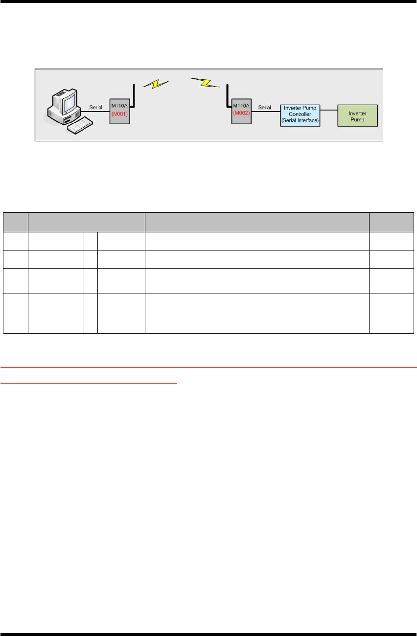
3.3.2 11 : SERIAL_WRITE
1) Description : Command that device with serial interface (M110A, W110A) in
DEVICE MODE becomes SOURCE, then transmit control signal data to
DESTINATION device with serial interface function in DEVICE MODE.
2) Send Data :
=> Control Signal DATA : MAX 20Byte
=> S/O/F
▸ S : Data Send
3) Control Signal DATA Value Range : MAX 20Byte
4) ACK Data :
=> DATA : Blank
=> S/O/F
▸ O : Data Receive OK
▸ F : Data Receive Fail
5) Applicable products :
▸ SOURCE : M110A(DEVICE MODE)
▸ DESTINATION : M110A(DEVICE MODE)
6) Example-1 : Serial Interface of PC MODE to PC MODE
▸ M110A(DEVICE MODE) : Serial Interface
▸ M110A(DEVICE MODE) : Serial Interface
▸ Configuration :
Figure 9. WRITE_SERIAL communication configuration example_1
- Control Signal Data = Inverter Pump open

Programmer's Guide_20110718_eng.hwp 15
Flow Data Flow Data Format Status
1 PC àM001 Pump Open Control Signal Data send Wire
2 M001 àM002 M00111@/M002SR00(CRC)↵Wireless
3 M001 ßM002 ▸ M00211@/M001FR00(CRC)↵ -> Fail ACK
▸ M00211@/M001OR00(CRC)↵ -> OK ACK Wireless
4
Inverter
Pump
Controller
ßM002 ▸ Pump Open Action -> OK ACK
▸ -> Fail ACK Wire
※ Cautions in using DEVICE MODE :
1. When data is sent through serial port, data must be sent at once without delay.
2. Only WRITE_SERIAL function can be used.
Programmer's Guide_20110718_eng.hwp 16
3.3.3 20 : READ
1) Description : Command that device with serial interface in PC MODE (M110A,
W110A) becomes SOURCE, then ask current received value from DESTINATION
device in PC MODE with DI[Digital Input], AI[Analog Input] function.
2) Send Data :
=> DATA : Blank
=> S/O/F
▸ S : Data Send
3) DATA Value Range : None
4) ACK Data :
=> READ_RESPONSE(21) is used as ACK for READ(20).
5) Applicable products : W110A , W210A, W310A, W410A
6) Example :
▸ M110A(PC MODE) : Serial Interface
▸ W310A(PC MODE) : DI[Digital Input] Interface
▸ Configuration :
Figure 11. READ communication configuration example
- Case that Destination with AI, DI function is requested to measure the current
input signal.
Flow Data Flow Data Format Status
1 PC àM001 M00120@/W001↵Wire
2 M001 àW001 M00120@/W001SR00↵Wireless

Programmer's Guide_20110718_eng.hwp 17
3.3.4 21 : READ_RESPONSE
1) Description : Command that SOURCE device with DI[Digital Input], AI[Analog
Input] function in PC MODE measures current input value and transmits
DESTINATION device requesting measured value. If 20(READ) is received,
measures and transmits current input value.
2) Send Data :
=> DATA : DI[Digital Input], AI[Analog Input] acquisition data
▸ W210A : *AI0(4Byte)*AI1(4Byte)*
▸ W310A, W410A : *DI(2Byte)*
=> S/O/F
▸ S : Data Send
3) Value Range of DATA
▸ DI : ※Current applied products are W110A, W310A, W410A
Classification Digital Port
Note
Name DI#7 DI#6 DI#5 DI#4 DI#3 DI#2 DI#1 DI#0
Signal Range 0~1 0~1 0~1 0~1 0~1 0~1 0~1 0~1 1="High",
0="Low"
Data Range
(Char) 0 ~ F 0 ~ F
Description
8 DI Ports are expressed in Bit as
Express 0x00 ~ 0xFF(Hex) in CHAR(2Byte)
Ex) Express 0xF0(Hex) -> F0(Char)
- Example :
Data order DI 1st Byte DI 2nd Byte
Note
Port Num DI#7 DI#6 DI#5 DI#4 DI#3 DI#2 DI#1 DI#0
Output Signal 1 1 1 1 1 1 1 1 1="High",
0="Low"
DI Data
Value F F
Description DI#0 ~ DI#7 Set all “High"
=> DATA = *FF*

Programmer's Guide_20110718_eng.hwp 18
※ W410A has 4 DI[Digital Input] Ports. So, DI 1st Byte is '0'.
▸ AI : ※ Current applied product is W210A(16Bit resolution)
Classification Analog Port
Note
Name AI#0 AI#1
Signal Range 0~5V, 0~10V, 0~20mA 0~5V, 0~10V, 0~20mA
Data Range
(Char) 0000~FFFF(16Bit) 0000~FFFF(16Bit)
Description
0~5V : 0V->0000, 5V->FFFF
0~10V : 0V->0000, 10V->FFFF
0~20mA : 0mA->0000, 20mA->FFFF
AI0, AI1 is generated proportionally in 16
bit
resolution (0000~FFFF(HEX)) depending on
the
setup input value range.
- Example :
Classification Analog Port
Note
Port Num AI#0 AI#1
Input Signal 5V when 0~5V 0V when 0~10V
AI Data
Value FFFF 0000
Description AI Data Value is an approximate value
=> DATA = *FFFF*0000*
Programmer's Guide_20110718_eng.hwp 19
4)ACK Data :
=> DATA : Blank
=> S/O/F
▸ O : Data Receive OK
▸ F : Data Receive Fail
5) Applicable products : W110A , W210A, W310A, W410A
6) Example :
▸ M110A(PC MODE) : Serial Interface
▸ W310A(PC MODE) : DI[Digital Input] Interface
▸ Configuration :
Figure 12. READ_RESPONSE communication configuration example
- DI Range : 00~FF(HEX)
- Acquisition case : DI = FF
Flow Data Flow Data Format Status
1 M001 ßW001 W00121@*FF*/M001SR00↵Wireless
2 M001 àW001 ▸ M00121@/W001FR00↵ -> Fail ACK
▸ M00121@/W001OR00↵ -> OK ACK Wireless
3 PC ßM001 ▸ W00121@*FF*/M001SR00↵-> case OK
▸ -> case Fail Wire
Programmer's Guide_20110718_eng.hwp 20
3.3.5 22 : STATUS_READ
1) Description : Command that device with Serial interface in PC MODE (M110A,
W110A) becomes SOURCE, then requests DESTINATION device with AO[Analog
Output], DO[Digital Output] function in PC MODE about current output value.
2) Send Data :
=> DATA : Blank
=> S/O/F
▸ S : Data Send
3) Value Range of DATA : None
4) ACK Data :
=> STATUS_RESPONSE(23) is used as ACK for STATUS_READ(22).
5) Applicable products : W110A , W310A, W510A
6) Example :
▸ M110A(PC MODE) : Serial Interface
▸ W310A(PC MODE) : DO[Digital Output] Interface
▸ Configuration :
Figure 13. READ communication configuration example
- Case that Destination with DO, AO function is requested to measure the current
output signal value.
Flow Data Flow Data Format Status
1 PC àM001 M00122@/W001↵Wire
2 M001 àW001 M00122@/W001SR00↵Wireless
Programmer's Guide_20110718_eng.hwp 21
3.3.6 23 : STATUS_RESPONSE
1) Description : Command that SOURCE device with AO[Analog Output], DO[Digital
Output] function in PC MODE transmits current output value to DESTINATION
device requesting output value.
2) Send Data :
=> DATA : DO[Digital Output], AO[Analog Output] Output Data
▸ W110A, W310A : *DO(2Byte)*
▸ W510A : *AO0(4Byte)*AO1(4Byte)*
=> S/O/F
▸ S : Data Send
3) Value Range of DATA : Same as 10(WRITE) command
4) ACK Data :
=> DATA : Blank
=> S/O/F
▸ O : Data Receive OK
▸ F : Data Receive Fail
5) Applicable products : W110A, W310A, W510A
6) Example :
▸ M110A(PC MODE) : Serial Interface
▸ W310A(PC MODE) : DO[Digital Output] Interface
▸ Configuration :
Figure 14. STATUS_RESPONSE communication configuration example

Programmer's Guide_20110718_eng.hwp 22
- DO Range : 00~FF(HEX)
- Output case : DO = FF
Flow Data Flow Data Format Status
1 M001 ßW001 W00123@*FF*/M001SR00↵Wireless
2 M001 àW001 ▸ M00123@/W001FR00↵ -> Fail ACK
▸ M00123@/W001OR00↵ -> OK ACK Wireless
3 PC ßM001 ▸ W00123@*FF*/M001SR00↵-> case OK
▸ -> case Fail Wire
Programmer's Guide_20110718_eng.hwp 23
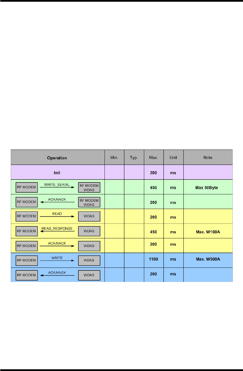
4. Communication Consumption Time
Intial booting time needed for normal operation after power on is about 200ms. In
serial data transmission (maximum 50Byte), it takes 450ms. Total time up to normal
ACK/NACK receiving takes 650ms. Also, total time for receiving READ command
and READ_RESPONSE, then transmitting ACK/NACK and for receiving
STATUS_READ command and STATUS_RESPONSE, then transmitting ACK/NACK
takes about 850ms. It takes about 400ms for transmitting WRITE command and
receiving ACK/NACK. However, in W500A case, it takes up to 1100ms. Users
should use products considering the communication consumption time.
(Communication consumption time is a time with some spare time. Consumption time
becomes longer when transmitting data length by RF becomes longer.) when users
send repeated data through RF MODEM, WDAS, ACK/NACK must be checked.
All device has silent period between transmission 10 seconds.
Table 3. Communication consumption time
Programmer's Guide_20110718_eng.hwp 24
5. Example
(EX 1) M110A(DEVICE MODE) to M110A(DEVICE MODES) communication
Figure 17. WRITE_SERIAL communication configuration example_1
- Control Signal Data = Inverter Pump open
Flow Data Flow Data Format Status
1 PC àM001 Pump Open Control Signal Data send Wire
2 M001 àM002 M00111@/M002SR00(CRC)↵Wireless
3 M001 ßM002 ▸ M00211@/M001FR00(CRC)↵ -> Fail ACK
▸ M00211@/M001OR00(CRC)↵ -> OK ACK Wireless
4
Inverter
Pump
Controller
ßM002 ▸ Pump Open Action -> OK ACK
▸ -> Fail ACK Wire
※ Caution in using DEVICE MODE : When data is sent through serial port, data
must be sent at once without delay.
Programmer's Guide_20110718_eng.hwp 25
(EX 2) M110A(PC MODE) to W110A(Only PC MODE) communication
Figure 18. M110A to W110A communication example
1. DO Control
W110A : DO#0, DO#1, DO#4, DO#5 output is desired
Flow Data Flow Data Format Status
1 PC àM001 M00110@*33*/W001↵Wire
2 M001 àW001 M00110@*33*/W001SR00↵Wireless
3 W001 àDevice DO#0, DO#1, DO#4, DO#5 => "High[=1]" Output Wire
4 M001 ßW001 ▸ W00110@/M001FR00↵ -> Fail ACK
▸ W00110@/M001OR00↵ -> OK ACK Wireless
5 PC ßM001 ▸ W00110@/M001FR00↵ -> Fail ACK
▸ W00110@/M001OR00↵ -> OK ACK Wire
2. Read AI, DI Status
Flow Data Flow Data Format Status
1 PC àM001 M00120@/W001↵Wire
2 M001 àW001 M00120@/W001SR00↵Wireless
3 W001 ßSensors Analog Input, Digital Input Signal Read Wire

Programmer's Guide_20110718_eng.hwp 26
3. AI, DI Data Transmission
(AI0 = 0x03FF, AI1 = 0x03FF, AI2 = 0x03FF, AI3 = 0x03FF, AI4 = 0x03FF, Digital
Input Data = 0xFF )
Flow Data Flow Data Format Status
1 M001 ßW001 W00121@*03FF*03FF*03FF*03FF*03FF*FF*/M001S
R00↵Wireless
2 M001 àW001 ▸ M00121@/W001FR00↵ -> Fail ACK
▸ M00121@/W001OR00↵ -> OK ACK Wireless
3 PC ßM001
▸W00121@*03FF*03FF*03FF*03FF*03FF*FF*/M00
1SR00↵ -> case OK
▸ -> case Fail
Wire
Programmer's Guide_20110718_eng.hwp 27
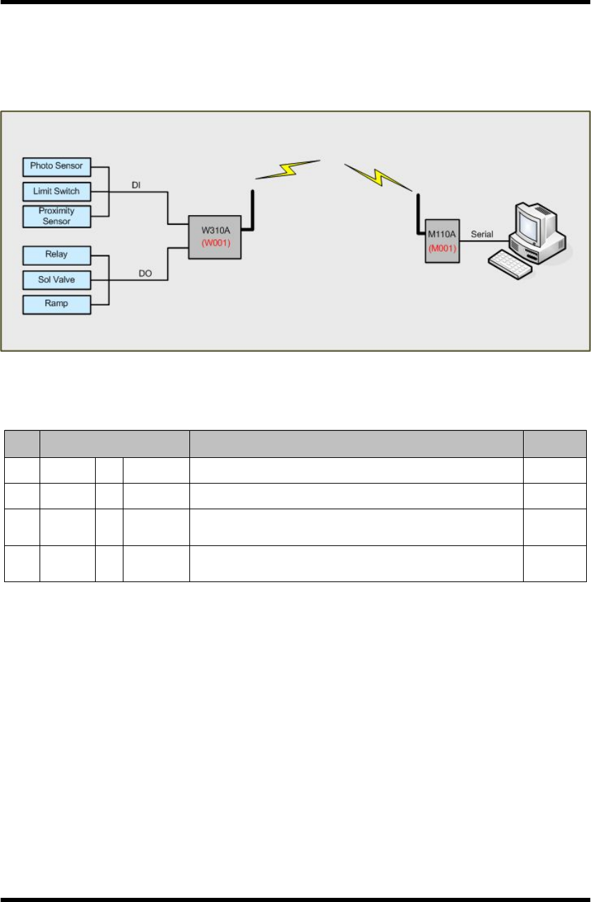
(EX 3) W210A(PC MODE) to M110A(PC MODE) communication
Figure 19. W210A to M110A communication example
1. Read AI Status
Flow Data Flow Data Format Status
1 PC àM001 M00120@/W001↵Wire
2 M001 àW001 M00120@/W001SR00↵Wireless
3 W001 ßSensors Analog Input Signal Read Wire
2. AI Data Transmission(Analog Input Data AI0 = FFFF, AI1 = 0000)
Flow Data Flow Data Format Status
1 M001 ßW001 W00121@*FFFF*0000*/M001SR00↵Wireless
2 M001 àW001 ▸ M00121@/W001FR00↵ -> Fail ACK
▸ M00121@/W001OR00↵ -> OK ACK Wireless
3 PC ßM001
▸ W00121@*FFFF*0000*/M001SR00↵
-> case OK
▸ -> case Fail
Wire
Programmer's Guide_20110718_eng.hwp 28
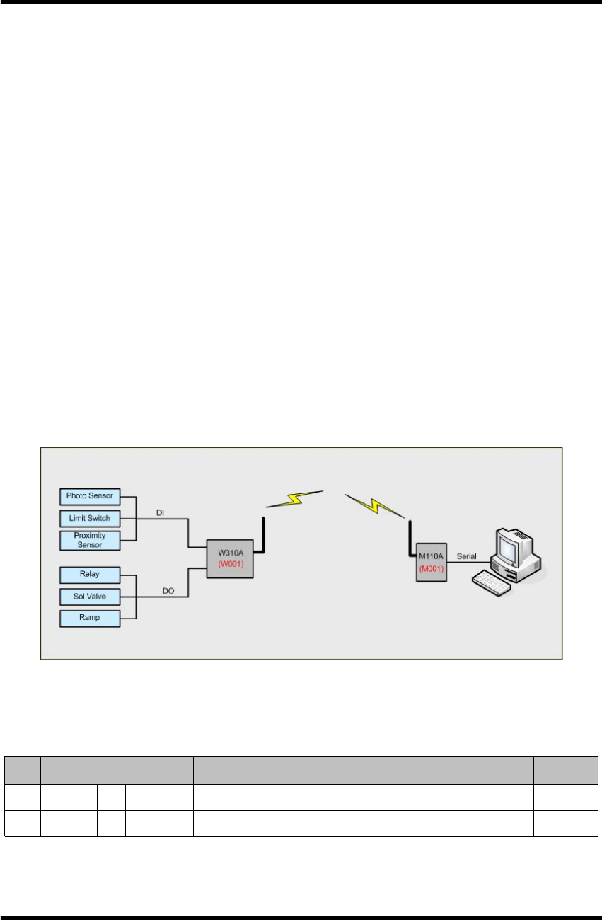
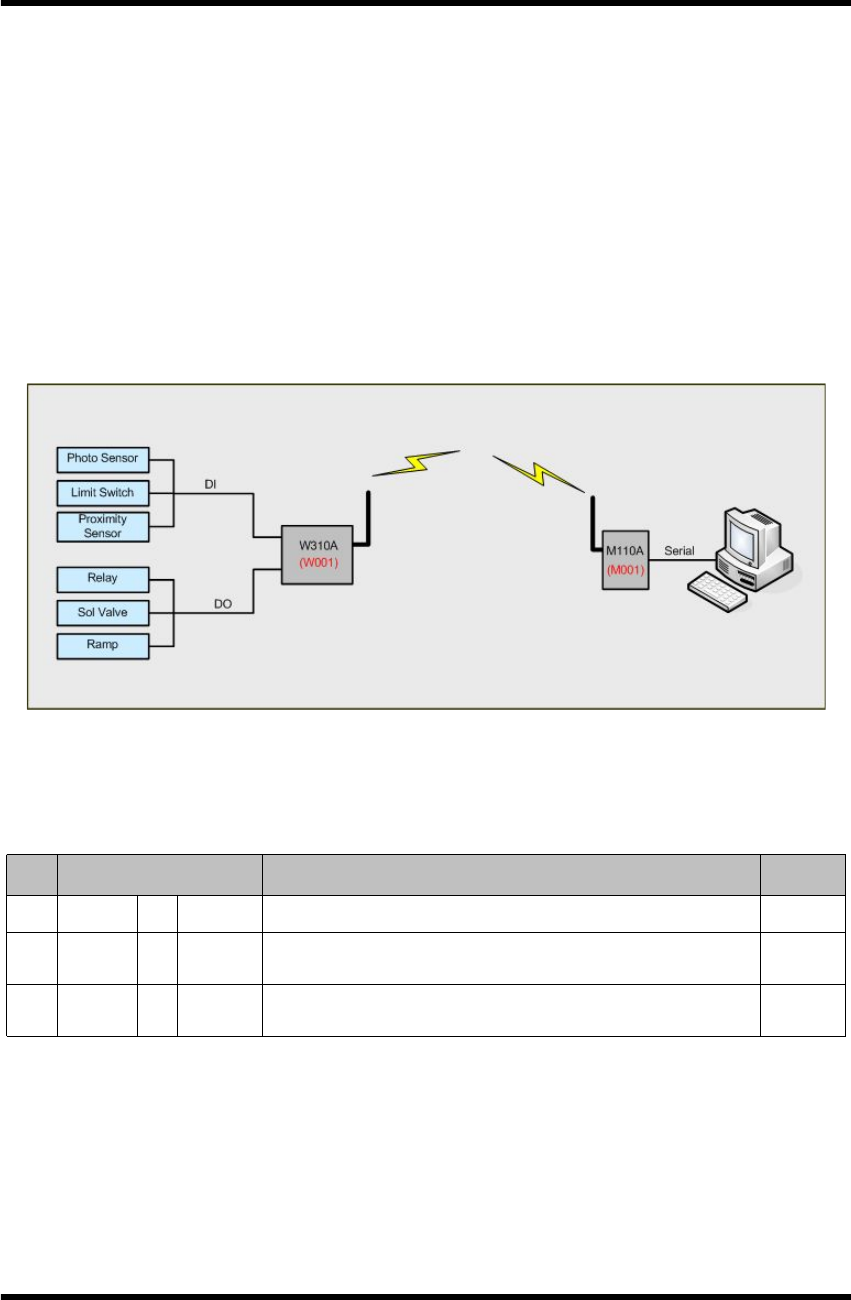
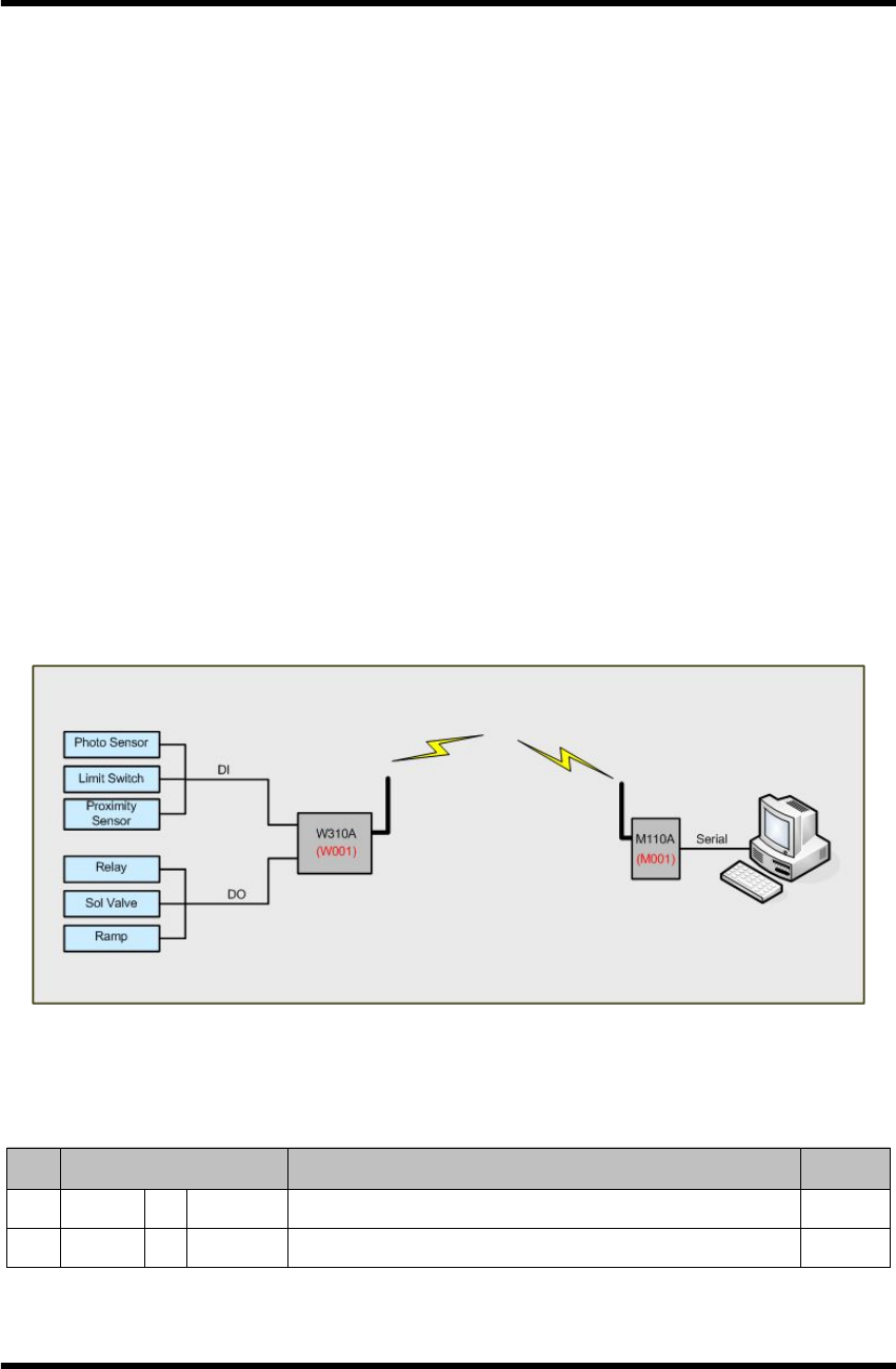
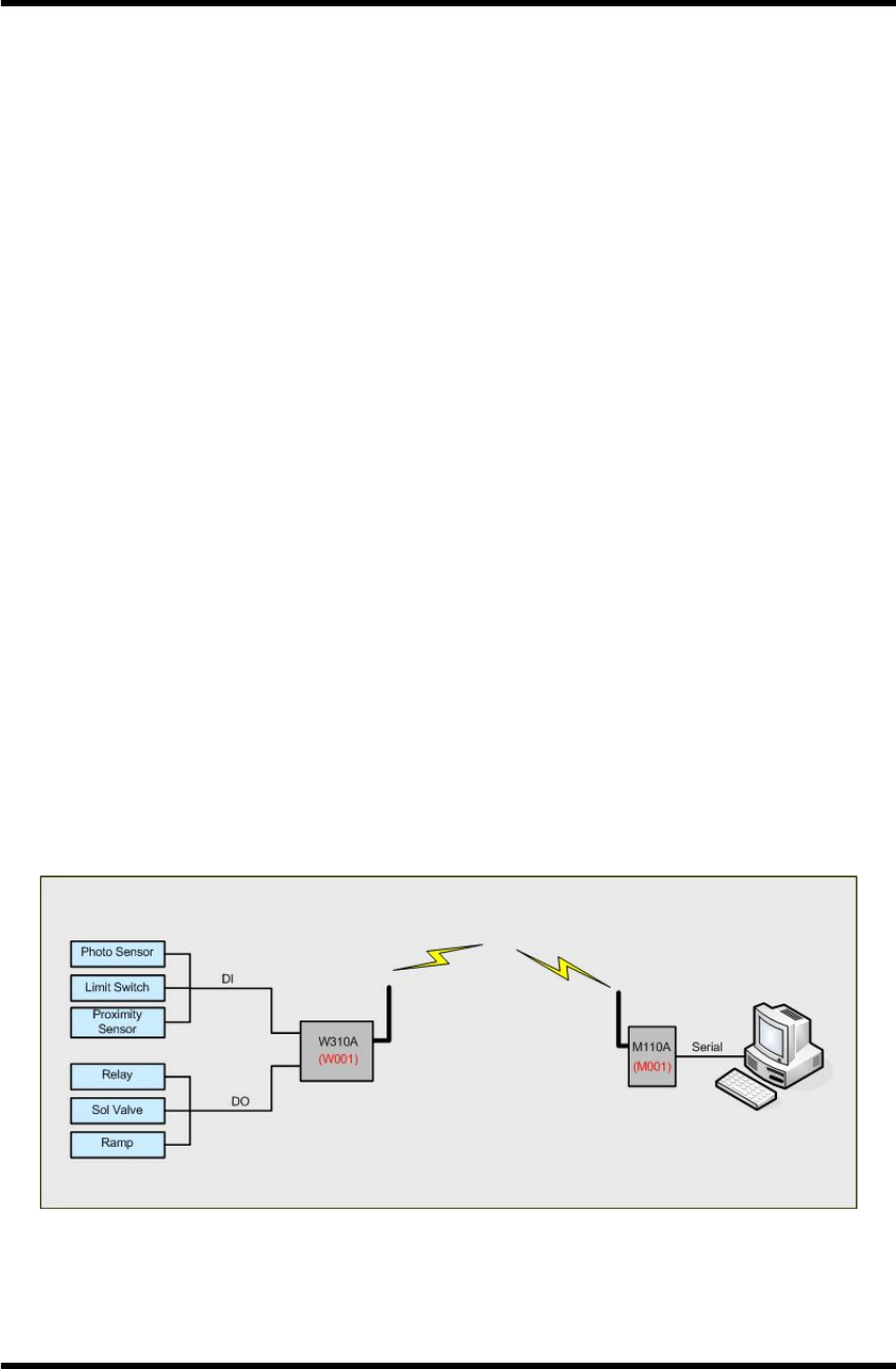
(EX 4) W310A(PC MODE) to M110A(PC MODE) communication
Figure 22. W310A to M110A communication example
1. DO Control
W310A : DO#0, DO#1, DO#4, DO#5 output is desired
Flow Data Flow Data Format Status
1 PC àM001 M00110@*33*/W001↵Wire
2 M001 àW001 M00110@*33*/W001SR00↵Wireless
3 W001 àDevice DO#0, DO#1, DO#4, DO#5 => "High[=1]" Set Wire
4 M001 ßW001 ▸ W00110@/M001FR00↵ -> Fail ACK
▸ W00110@/M001OR00↵ -> OK ACK Wireless
5 PC ßM001 ▸ W00110@/M001FR00↵ -> Fail ACK
▸ W00110@/M001OR00↵ -> OK ACK Wire
2. Read DI Status
Flow Data Flow Data Format Status
1 PC àM001 M00120@/W001↵Wire
2 M001 àW001 M00120@/W001SR00↵Wireless
3 W001 ßSensors Digital Input Signal Read Wire

Programmer's Guide_20110718_eng.hwp 29
3. DI Data Transmission(Digital Input Data = 0xFF)
Flow Data Flow Data Format Status
1 M001 ßW001 W00121@*FF*/M001SR00↵Wireless
2 M001 àW001 ▸ M00121@/W001FR00↵ -> Fail ACK
▸ M00121@/W001OR00↵ -> OK ACK Wireless
3 PC ßM001 ▸ W00121@*FF*/M001SR00↵-> case OK
▸ -> case Fail Wire
Programmer's Guide_20110718_eng.hwp 30
(EX 5) W410A(PC MODE) to M110A(PC MODE) communication
Figure 25. W410A to M110A communication example
1. Read DI Status
Flow Data Flow Data Format Status
1 PC àM001 M00120@/W001↵Wire
2 M001 àW001 M00120@/W001SR00(CRC)↵Wireless
3 W001 ßSensors Digital Input Signal Read Wire
2. DI Data Transmission (Digital Input Data = 0x0F)
Flow Data Flow Data Format Status
1 M001 ßW001 W00121@*0F*/M001SR00↵Wireless
2 M001 àW001 ▸ M00121@/W001FR00↵ -> Fail ACK
▸ M00121@/W001OR00↵ -> OK ACK Wireless
3 PC ßM001 ▸ W00121@*0F*/M001SR00↵ -> case OK
▸ -> case Fail Wire
Programmer's Guide_20110718_eng.hwp 31
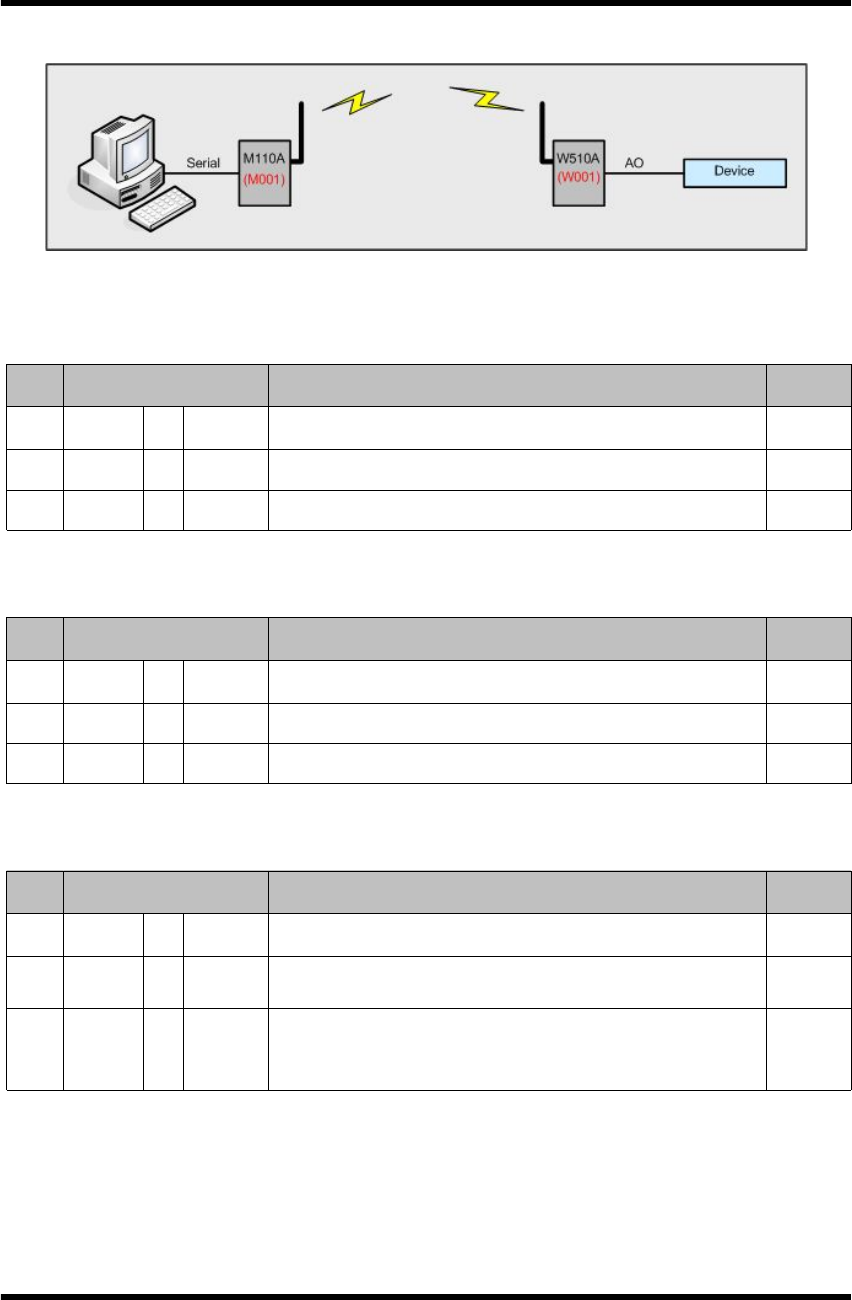
(EX 6) W510A(PC MODE) to M110A(PC MODE) communication
Figure 27. W510A to M110A communication example
1. AO Control
Flow Data Flow Data Format Status
1 PC àM001 M00110@*FFFF*FFFF*/W001↵Wire
2 M001 àW001 M00110@*FFFF*FFFF*/W001SR00↵Wireless
3 W001 àDevice Analog Output Signal Write Wire
2. Read AO Status
Flow Data Flow Data Format Status
1 PC àM001 M00122@/W001↵Wire
2 M001 àW001 M00122@/W001SR00↵Wireless
3 W001 ßSensors Analog Output Signal Read Wire
3. AO Status Transmission (Analog Output Data : AO0=0xFFFF, AO1=0xFFFF)
Flow Data Flow Data Format Status
1 M001 ßW001 W00123@*03FF*03FF*/M001SR00↵Wireless
2 M001 àW001 ▸ M00123@/W001FR00↵ -> Fail ACK
▸ M00123@/W001OR00↵ -> OK ACK Wireless
3 PC ßM001
▸ W00123@*FFFF*FFFF*/M001SR00↵
-> case OK
▸ -> case Fail
Wire

Programmer's Guide_20110718_eng.hwp 32
Appendix 1. Document Information
Revision Description
1.0 07/13/2011 - Initial Release Version

Programmer's Guide_20110718_eng.hwp 33
SEBINE Technology, Inc.
Homepage : www.sebinetech.com
E-mail : tech@sebinetech.com
RN 202, Daedeok Radio Engineering Center, 694, Tamnip-dong, Yuseong-gu,
Daejeon, Korea 305-510
Tel : 82-42-935-2084, 2085
Fax : 82-42-935-2088