SIMCom Wireless Solutions 201802 LTE-FDD MODULE User Manual 2AJYU 201802 User Manual REV 2
Shanghai SIMCom Wireless Solutions Limited LTE-FDD MODULE 2AJYU 201802 User Manual REV 2
UserManual.wiki
>
SIMCom Wireless Solutions
>
201802 User Manual
2AJYU-201802_User_Manual_REV 2
Navigation menu
Upload a User Manual
Namespaces
Wiki Guide
HTML
PDF
Info
Views
User Manual
Discussion / Help
Navigation
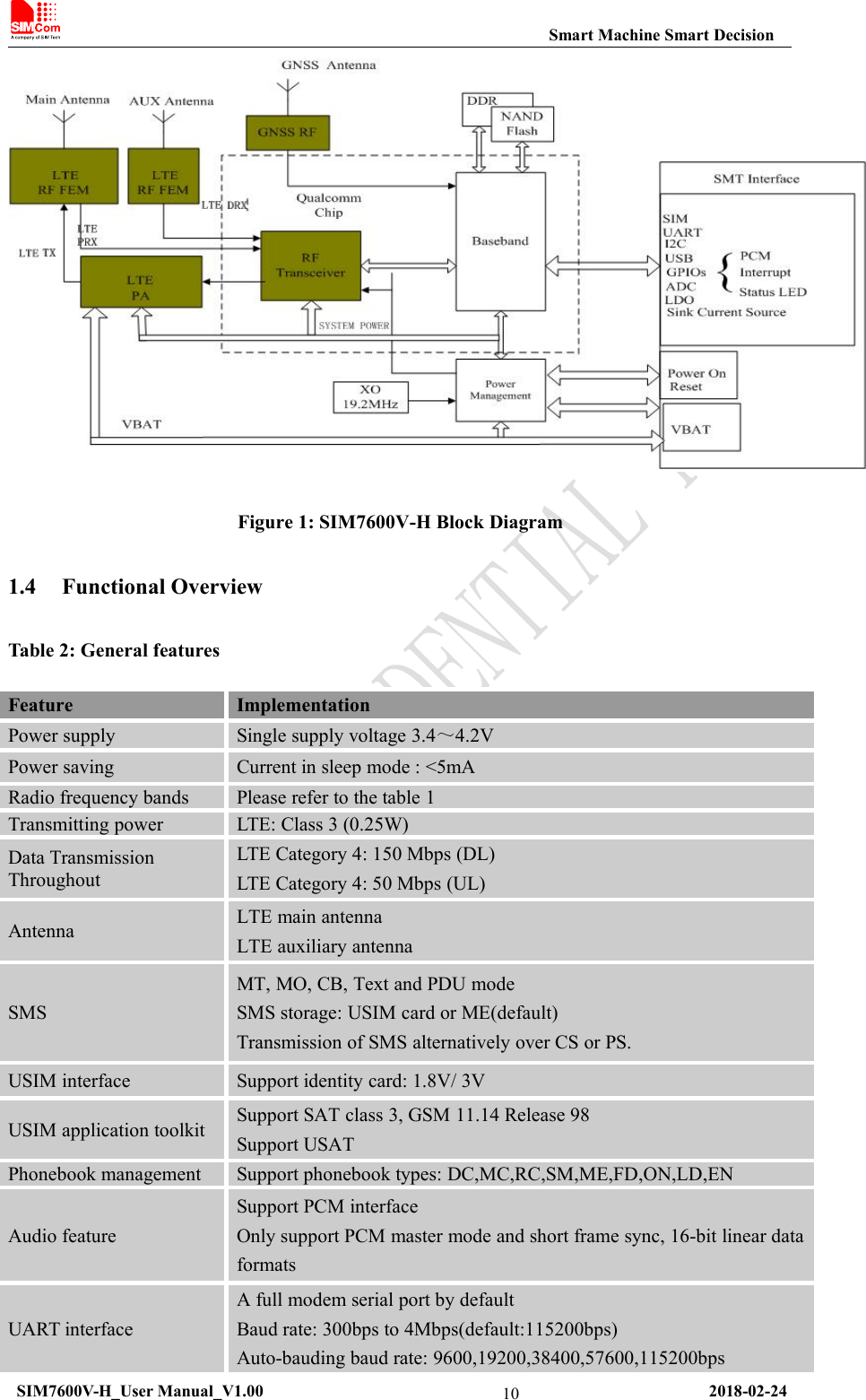
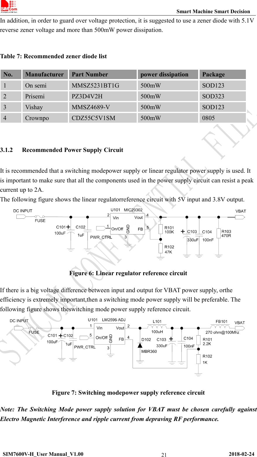
![Smart Machine Smart DecisionSIM7600V-H_User Manual_V1.00 2018-02-24223.1.3 Voltage MonitorTo monitor the VBAT voltage, the AT command “AT+CBC” can be used.For monitoring the VBAT voltage outside or within a special range, the AT command“AT+CVALARM” can be used to enable the under-voltage warning function.If users need to power off Module, when the VBAT voltage is out of a range, the AT command“AT+CPMVT” can be used to enable under-voltage power-off function.Note: Under-voltage warning function and under-voltage power-off function are disabled bydefault. For more information about these AT commands, please refer to Document [1].3.2 Power on/Power off/Reset Function3.2.1 Power onModule can be powered on by pulling the PWRKEY pin down to ground.The PWRKEY pin has been pulled up to dVDDinternally, so you does not need to pull it upexternally. It is strongly recommended to put a100nF capacitor and an ESD protection diode closeto the PWRKEY pin. Please refer to the following figure for the recommended reference circuit.47KPWRKEY PowerOn off logicDiodedVDDMODULE100Ω100nF4.7KTurn on /offimpulseFigure 8: ReferencePower on/off circuitThe power-on scenarios are illustrated in the following figure.](https://usermanual.wiki/SIMCom-Wireless-Solutions/201802/User-Guide-3818358-Page-22.png)
![Smart Machine Smart DecisionSIM7600V-H_User Manual_V1.00 2018-02-2424For details about “AT+CPOF” and “AT+CPMVT”, please refer to Document [1].These procedures will make modules disconnect from the network and allow the software to enter asafe state and save data before modules are powered off completely.The power off scenario by pulling down the PWRKEY pin is illustrated in the following figure.(Output)Toff( Input )Toff(status)UART Port UndefinedActiveToff(uart)TonToff-onUSB Port UndefinedActiveToff(usb)PWRKEYSTATUSFigure 10: Power off timing sequenceTable 9: Power off timing and Electronic CharacteristicSymbolParameterTime valueUnitMin.Typ.Max.ToffThe active low level time pulse on PWRKEY pin topower off module2.5----sToff(status)The time from power-off issue to STATUS pin outputlow level(indicating power off )*22--sToff(uart)The time from power-off issue to UART port off15--sToff(usb)The time from power-off issue to USB port off15--sToff-onThe buffer time from power-off issue to power-onissue0--s3.2.3 Reset FunctionModule can be reset by pulling the RESET pin down to ground.Note: This function is only used as an emergency reset when AT command “AT+CPOF” and thePWRKEY pin all have lost efficacy.](https://usermanual.wiki/SIMCom-Wireless-Solutions/201802/User-Guide-3818358-Page-24.png)
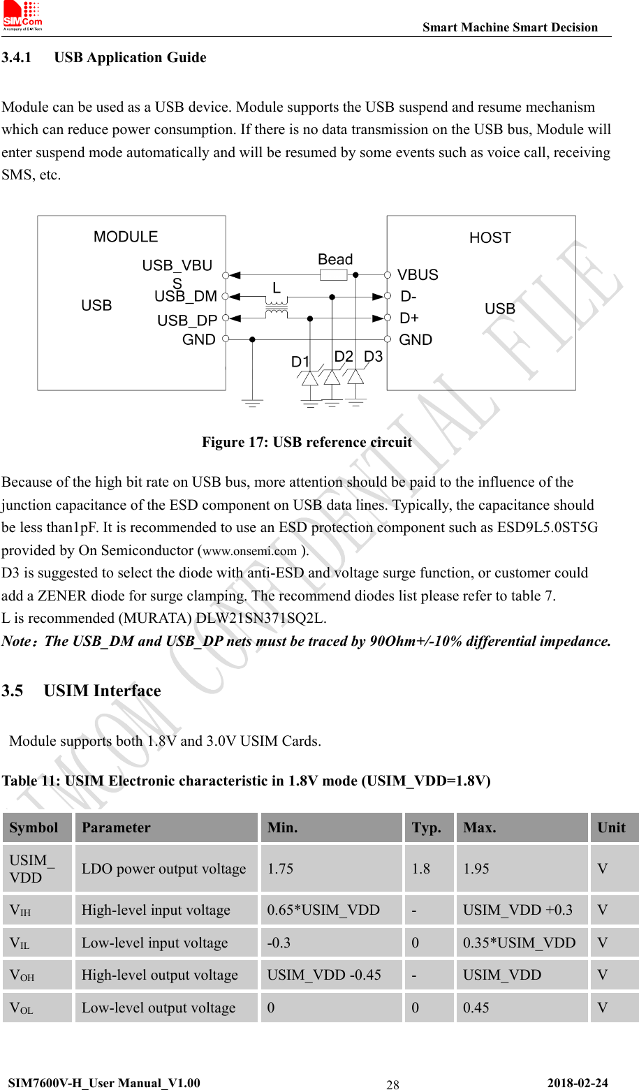
![Smart Machine Smart DecisionSIM7600V-H_User Manual_V1.00 2018-02-24273.3.2 RI and DTR BehaviorThe RI pin can be used to interrupt output signal to inform the host controller such as applicationCPU.Normally RI will stay at high level until certain conditions such as receiving SMS, or a URC reportcome in. It will then change to low level. It will stay low until the host controller clears theinterrupted event with “AT+CRIRS” AT command.Figure 15: RI behaviour(SMS and URC report)Normally RI will be kept high until a voice call, then it will output periodic rectangular wave with5900ms low level and 100ms high level. It will output this kind of periodic rectangular wave untilthe call is answered or hung up.Figure 16: RI behaviour(voice call)Note: For more details of AT commands about UART, please refer to document [1] and [22].DTR pin can be used to wake Module from sleep. When Module enters sleep mode, pulling downDTR can wake Module.3.4 USB InterfaceThe Module contains a USB interface compliant with the USB2.0 specification as a peripheral, butthe USB charging function is not supported.](https://usermanual.wiki/SIMCom-Wireless-Solutions/201802/User-Guide-3818358-Page-27.png)
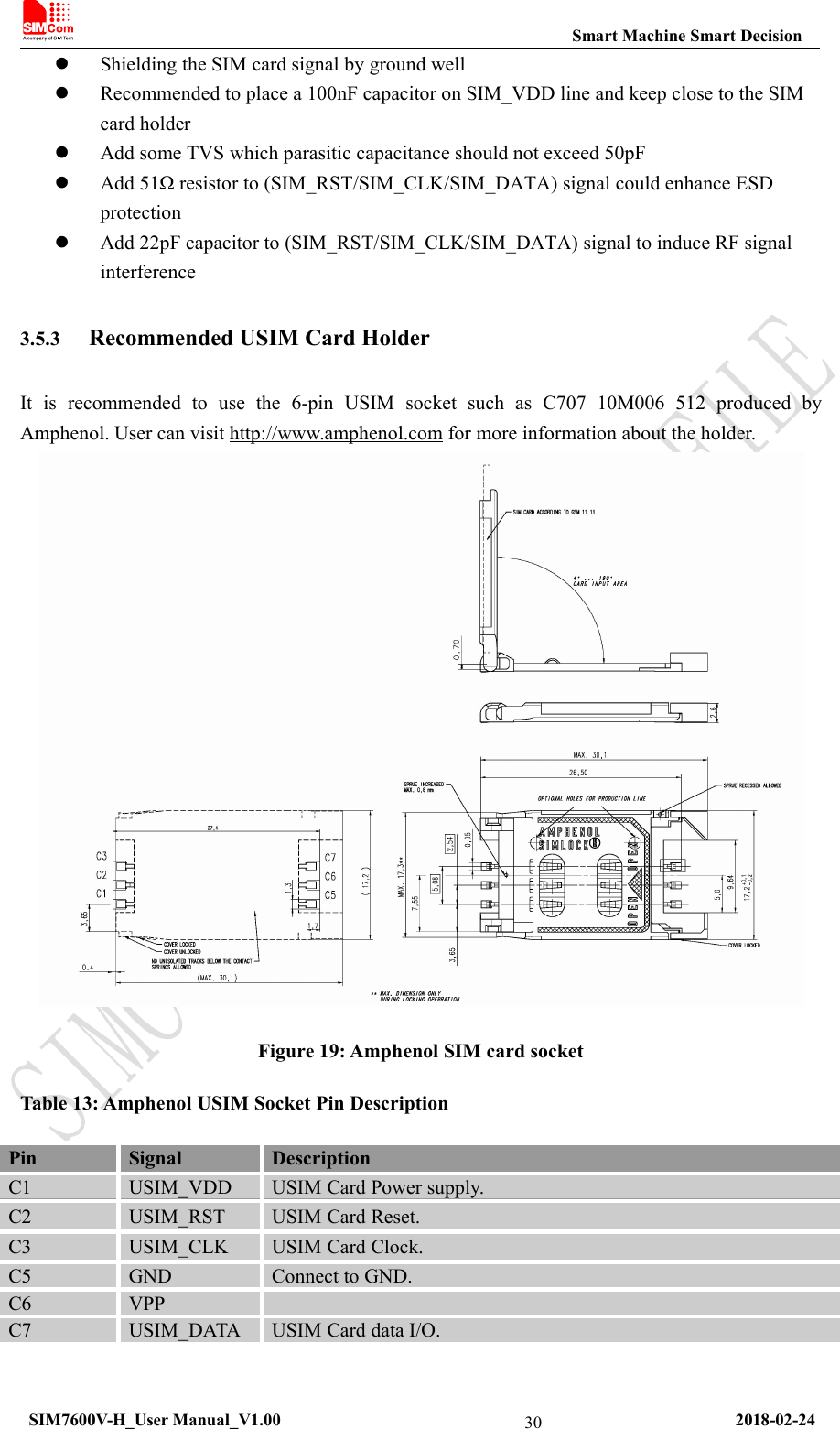
![Smart Machine Smart DecisionSIM7600V-H_User Manual_V1.00 2018-02-2429Table 12: USIM Electronic characteristic 3.0V mode (USIM_VDD=2.95V)SymbolParameterMin.Typ.Max.UnitUSIM_VDDLDO power output voltage2.752.953.05VVIHHigh-level input voltage0.65*USIM_VDD-USIM_VDD +0.3VVILLow-level input voltage-0.300.25*USIM_VDDVVOHHigh-level output voltageUSIM_VDD -0.45-USIM_VDDVVOLLow-level output voltage000.45V3.5.1 USIM Application GuideIt is recommended to use an ESD protection component such as ESDA6V1W5 produced by ST(www.st.com ) or SMF15C produced by ON SEMI (www.onsemi.com ). Note that the USIMperipheral circuit should be close to the USIM card socket.The following figure shows the 6-pinSIM card holder reference circuit.Figure 18: USIM interface reference circuitNote: USIM_DATA has been pulled up with a100KΩ resistor to USIM_VDD in module. A 100nFcapacitor on USIM_VDD is used to reduceinterference. For more details of AT commands aboutUSIM, please refer to document [1].3.5.2 SIM Card Design GuideSIM card signal could be interferenced by some high frequency signal, it is strongly recommendedto follow these guidelines while designing:SIM card holder should be far away from antennaSIM traces should keep away from RF lines, VBAT and high-speed signal linesThe traces should be as short as possibleKeep SIM card holder’s GND connect to main ground directly](https://usermanual.wiki/SIMCom-Wireless-Solutions/201802/User-Guide-3818358-Page-29.png)
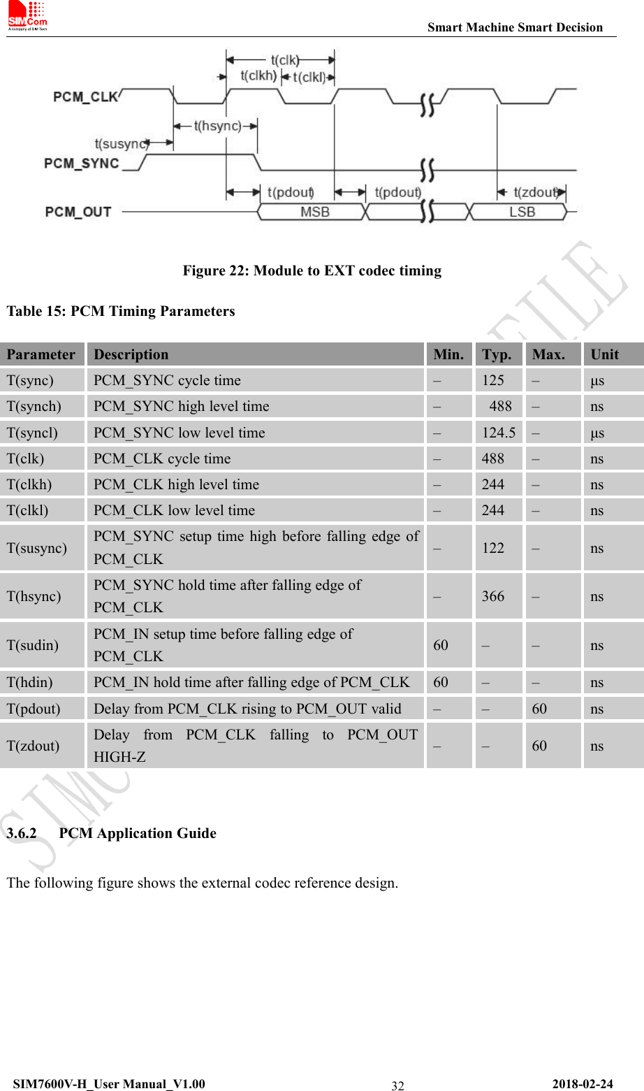
![Smart Machine Smart DecisionSIM7600V-H_User Manual_V1.00 2018-02-24313.6 PCM InterfaceModule provides a PCM interface for external codec, which can be used inmaster mode with shortsync and 16 bits linear format.Table 14: PCM FormatNote: For more details about PCM AT commands, please refer to document [1].3.6.1 PCM TimingModule supports 2.048 MHz PCM data and sync timing for 16 bits linear format codec.Figure 20: PCM_SYNC timingFigure 21: EXT codec to module timingCharacteristicsSpecificationLineInterfaceFormatLinear(Fixed)Datalength16bits(Fixed)PCM Clock/Sync SourceMaster Mode(Fixed)PCMClockRate2048 KHz (Fixed)PCMSyncFormatShortsync(Fixed)Data OrderingMSB](https://usermanual.wiki/SIMCom-Wireless-Solutions/201802/User-Guide-3818358-Page-31.png)
![Smart Machine Smart DecisionSIM7600V-H_User Manual_V1.00 2018-02-2433Figure 23: Audio codec reference circuitNote: Module can transmit PCM data by theUSB portbesidesthe PCM interface. For moredetails please refer to documents [1] and [23].3.7 I2C InterfaceModule provides a I2C interface compatible with I2C specification, version 2.1, with clock rate upto 400 kbps. Its operation voltage is 1.8V.3.7.1 I2C Design GuideThe following figure shows the I2C bus reference design.Figure 24: I2C reference circuitNote:SDA and SCLhave pull-up resistors in module. So, 2 external pull up resistors are not needed inapplication circuit.“AT+CRIIC and AT+CWIIC” AT commands could be used to read/write register values of theI2C peripheral devices.For more details about AT commands please refer to document [1].](https://usermanual.wiki/SIMCom-Wireless-Solutions/201802/User-Guide-3818358-Page-33.png)
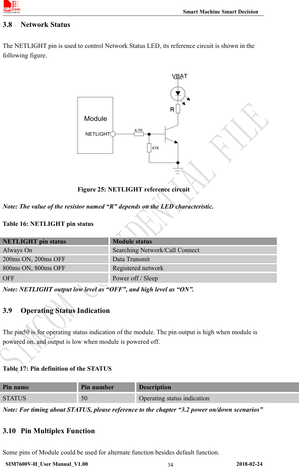
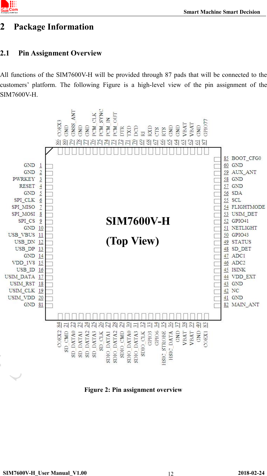
![Smart Machine Smart DecisionSIM7600V-H_User Manual_V1.00 2018-02-2435Table 18: Pin multiplex function listNote:For more details of AT commands about GPIO multiplex function,please refer todocument [1].3.11 Other interface3.11.1 Sink Current SourceThe ISINK pin is VBATtolerant and intended to drive some passive devices such as LCD backlight,white LED, etc. Its output current can be up to 40 mA and be set by the AT command “AT+CLEDITST”.Table 19: Sink current electronic characteristicSymbolDescriptionMin.Typ.Max.UnitVISINKVoltage tolerant0.5-VBATVIISINKCurrent tolerant0-40mAISINK is a ground-referenced current sink. The following figure shows its reference circuit.Figure 26: ISINK reference circuitPin NumberPin NameDefault FunctionAlternate Function4SCLSCLGPIO115SDASDAGPIO1012USIM_DETGPIO34USIM_DET18PCM_CLKPCM_CLKGPIO23,SPI_CLKI2C_SCL19PCM_SYNCPCM_SYNCGPIO20,SPI_MOSI20PCM_INPCM_IN,GPIO21,SPI_MISO21PCM_OUTPCM_OUTGPIO22,SPI_CS_NI2C_SDA](https://usermanual.wiki/SIMCom-Wireless-Solutions/201802/User-Guide-3818358-Page-35.png)
![Smart Machine Smart DecisionSIM7600V-H_User Manual_V1.00 2018-02-2436Note: The sinking current can be adjusted to meet the design requirement through the ATcommand “AT+ CLEDITST =<0>, <value>”.The “value” ranges from 0 to 8, on behalf of thecurrent from 0mA to 40mA by 5mA step.3.11.2 ADCModule has 1 dedicated ADC pins named ADC. They are available fordigitizing analog signalssuch as battery voltage and so on. These electronic specifications are shown in the following table.Table 20: ADC Electronic CharacteristicsCharacteristicsMin.Typ.Max.UnitResolution–15–BitsInput Range0.11.7VInput serial resistance1––MΩNote: “AT+CADC” can be used to read the voltage of the ADC pins, for more details, pleaserefer to document [1].](https://usermanual.wiki/SIMCom-Wireless-Solutions/201802/User-Guide-3818358-Page-36.png)
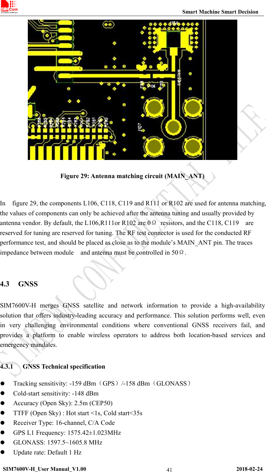
![Smart Machine Smart DecisionSIM7600V-H_User Manual_V1.00 2018-02-2439Figure 28: Antenna matching circuit (DIV_ANT)In above figure, R3, C3, C4 and R4 are used for auxiliary antenna matching. By default, the R3, R4are 0Ωresistors, and the C3, C4 are reserved for tuning. D2 is a TVS for ESD protection, and it isoptional for users according to application environment.Two TVS are recommended in the table below.Table 26: Recommended TVSPackagePart NumberVender0201LXES03AAA1-154Murata0402LXES15AAA1-153MurataNote:SIMCom suggests the LTE auxiliary antenna to be kept on, since there are many highbands in the designing of FDD-LTE. Because of the high insert loss of the RF cable and layoutlines, the receiver sensitivity of these bands above will have risk to meet the authenticationwithout the diversity antenna.For more details about auxiliary antenna design notice,pleaserefer to document [25]To facilitate the antenna tuning and certification test, a RF connector and an antenna matchingcircuit should be added. The following figure is the recommended circuit.circuit should be added. The following figure is the recommended circuit.](https://usermanual.wiki/SIMCom-Wireless-Solutions/201802/User-Guide-3818358-Page-39.png)
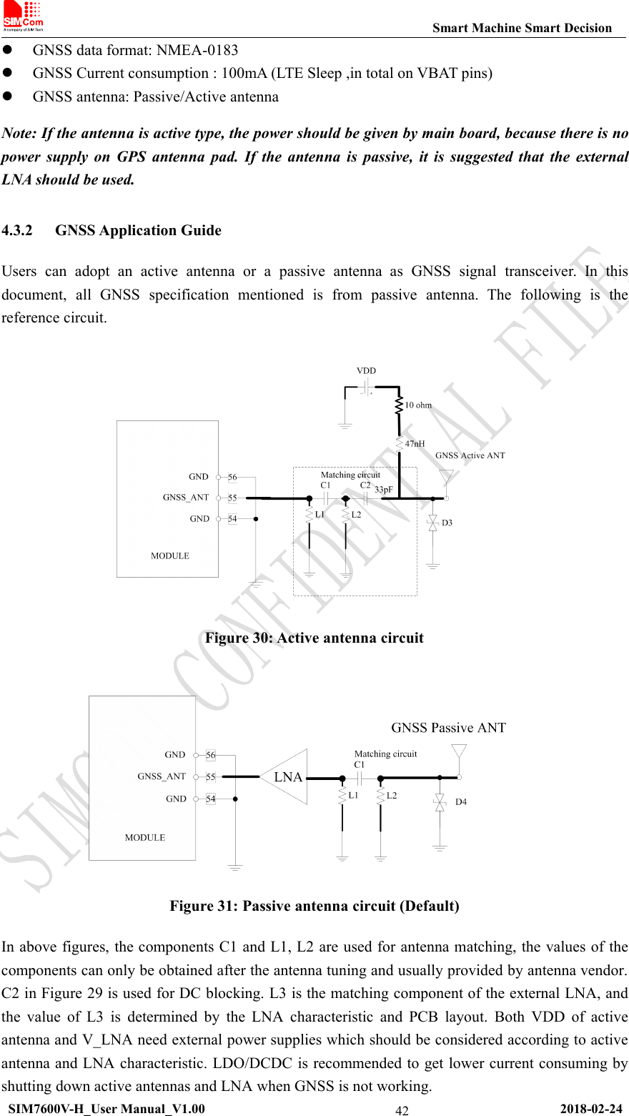
![Smart Machine Smart DecisionSIM7600V-H_User Manual_V1.00 2018-02-2443LNA should apply the following requirements as table 28. LNA is also suggested to put near thepassive antenna.Table 27: LNA requirementsParameterMinMaxUnitVdd1.53.3VIdd3mALNA_EN1.3VGain1417dBVSWR2GNSS can be used by NMEA port. User can select NMEA as output through UART or USB.NMEA sentences are automatic and no command is provided. NMEA sentences include GSV, GGA,RMC, GSA, and VTG. Before using GNSS, user should configure SIM7600V-H in properoperating mode by AT command. Please refer to related document for details. SIM7600V-H canalso get position location information through AT directly.Note: GNSS is closed by default, it could be started by AT+CGPS. The AT command has twoparameters, the first is on/off, and the second is GNSS mode. Default mode is standalone mode.AGPS mode needs more support from the mobile telecommunication network. Please refer todocument [24] for more details.](https://usermanual.wiki/SIMCom-Wireless-Solutions/201802/User-Guide-3818358-Page-43.png)
![Smart Machine Smart DecisionSIM7600V-H_User Manual_V1.00 2018-02-2446power supply. In this mode, the RF part of the module will not workbut the serial port and USB port are still accessible. The powerconsumption in this mode is lower than normal mode.Power offModule will go into power off mode by sending the AT command“AT+CPOF” or by pulling down the PWRKEY pin normally. In thismode the power management unit shuts down the power supply andsoftware is not active. The serial port and USB are is not accessible.5.3.2 Sleep ModeIn sleep mode, the current consumption of module will be reduced to the minimal level, andmodule can still receive paging message and SMS.Several hardware and software conditions must be satisfied together in order to let Module enterinto sleep mode:1. UART condition2. USB condition3. Software conditionNote: Before designing, pay attention to how to realize sleeping/waking function and refer toDocument [26] for more details.5.3.3 Minimum Functionality Mode and Flight ModeMinimum functionality mode ceasesa majority functionof module, thus minimizing the powerconsumption. This mode is set by the AT command which provides a choice of the functionalitylevels.●AT+CFUN=0: Minimum functionality●AT+CFUN=1: Full functionality (Default)●AT+CFUN=4: Flight modeIf Module has been set to minimum functionality mode, the RF function and USIM card functionwill be closed. In this case, the serial port and USB are still accessible, but RF function and USIMcard will be unavailable.If Module has been set to flight mode, the RF function will be closed. In this case, the serial portand USB are still accessible, but RF function will be unavailable.When Module is in minimum functionality or flight mode, it can return to full functionality by theAT command “AT+CFUN=1”.5.4 Current ConsumptionThe current consumption is listed in the table below.](https://usermanual.wiki/SIMCom-Wireless-Solutions/201802/User-Guide-3818358-Page-46.png)
![Smart Machine Smart DecisionSIM7600V-H_User Manual_V1.00 2018-02-24486SMT Production Guide6.1 Top and Bottom View of ModuleFigure 32: Top and bottom view of Module6.2 Typical SMT Reflow ProfileSIMCom provides a typical soldering profile. Therefore the soldering profile shown below is onlya generic recommendation and should be adjusted to the specific application and manufacturingconstraints.Figure 33: The ramp-soak-spike Reflow Profile of ModuleNote: For more details about secondary SMT, please refer to the document [21].](https://usermanual.wiki/SIMCom-Wireless-Solutions/201802/User-Guide-3818358-Page-48.png)
![Smart Machine Smart DecisionSIM7600V-H_User Manual_V1.00 2018-02-2455C. Related DocumentsTable 40: Related documentsSNTitleDescription[1]SIM7X00 Series_ATCommand Manual_V1.xxSIM7X00 Series_AT Command Manual[2]ITU-T Draft newrecommendationV.25terSerial asynchronous automatic dialing and control[3]GSM 07.07Digital cellular telecommunications (Phase 2+); AT commandset for GSM Mobile Equipment (ME)[4]GSM 07.10Support GSM 07.10 multiplexing protocol[5]GSM 07.05Digital cellular telecommunications (Phase 2+); Use of DataTerminal Equipment – Data Circuit terminating Equipment(DTE – DCE) interface for Short Message Service (SMS)and Cell Broadcast Service (CBS)[6]GSM 11.14Digital cellular telecommunications system (Phase 2+);Specification of the SIM Application Toolkit for theSubscriber Identity Module – Mobile Equipment (SIM – ME)interface[7]GSM 11.11Digital cellular telecommunications system (Phase 2+);Specification of the Subscriber Identity Module – MobileEquipment (SIM – ME) interface[8]GSM 03.38Digital cellular telecommunications system (Phase 2+);Alphabets and language-specific information[9]GSM 11.10Digital cellular telecommunications system (Phase 2) ;Mobile Station (MS) conformance specification ;Part 1:Conformance specification[10]3GPP TS 51.010-1Digital cellular telecommunications system (Release 5);Mobile Station (MS) conformance specification[11]3GPP TS 34.124Electromagnetic Compatibility (EMC) for mobile terminalsand ancillary equipment.[12]3GPP TS 34.121Electromagnetic Compatibility (EMC) for mobile terminalsand ancillary equipment.[13]3GPP TS 34.123-1Technical Specification Group Radio Access Network;Terminal conformance specification; Radio transmission andreception (FDD)[14]3GPP TS 34.123-3User Equipment (UE) conformance specification; Part 3:Abstract Test Suites.[15]EN 301 908-02 V2.2.1Electromagnetic compatibility and Radio spectrum Matters(ERM); Base Stations (BS) and User Equipment (UE) forIMT-2000. Third Generation cellular networks; Part 2:Harmonized EN for IMT-2000, CDMA Direct Spread(UTRA FDD) (UE) covering essential requirements of article3.2 of the R&TTE Directive[16]EN 301 489-24 V1.2.1Electromagnetic compatibility and Radio Spectrum Matters(ERM); Electromagnetic Compatibility (EMC) standard forradio equipment and services; Part 24: Specific conditions forIMT-2000 CDMA Direct Spread (UTRA) for Mobile andportable (UE) radio and ancillary equipment[17]IEC/EN60950-1(2001)Safety of information technology equipment (2000)[18]3GPP TS 51.010-1Digital cellular telecommunications system (Release 5);Mobile Station (MS) conformance specification](https://usermanual.wiki/SIMCom-Wireless-Solutions/201802/User-Guide-3818358-Page-55.png)
![Smart Machine Smart DecisionSIM7600V-H_User Manual_V1.00 2018-02-2456[19]GCF-CC V3.23.1Global Certification Forum - Certification Criteria[20]2002/95/ECDirective of the European Parliament and of the Council of27 January 2003 on the restriction of the use of certainhazardous substances in electrical and electronic equipment(RoHS)[21]Modulesecondary-SMT-UGD-V1.xxModule secondary SMT Guidelines[22]SIM7X00Series_UART_ApplicationNote_V1.xxSIM7X00 Series_UART_Application Note[23]SIM7X00 Series_USBAUDIO_ApplicationNote_V1.xxSIM7X00 Series_USB AUDIO_Application Note[24]Antenna design guidelines fordiversity receiver systemAntenna design guidelines for diversity receiver system[25]SIM7X00 Series_Sleep Mode_Application Note_V1.xxSIM7X00 Series_Sleep Mode_ Application Note](https://usermanual.wiki/SIMCom-Wireless-Solutions/201802/User-Guide-3818358-Page-56.png)