ST Microelectronics S R L
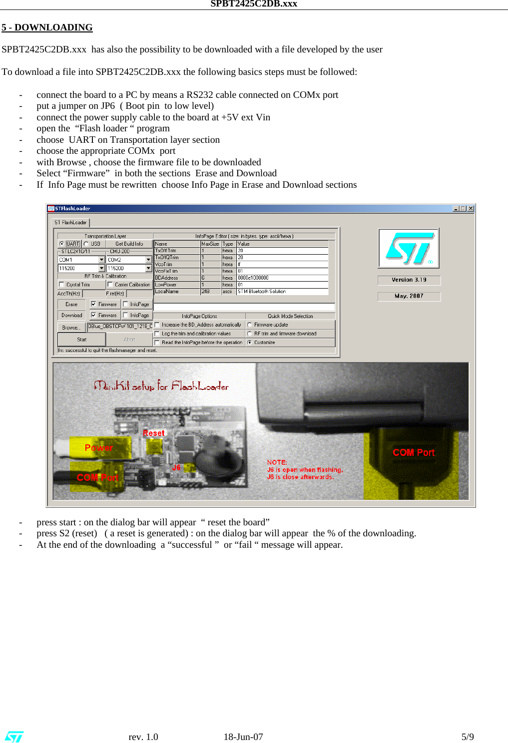
 2425C2DB Bluetooth class 2 module User Manual SPBT2425C2DBxxx V01

ST Microelectronics S.R.L. Bluetooth class 2 module SPBT2425C2DBxxx V01

Contents

Users Manual I

                           SPBT2425C2DB.xxx User Manual                                                                                                                                                                            June 2007  FEATURES  - Bluetooth V2.0 board - Serial interface on DB9 connector - USB connection - PCB antenna on board - Single 5 V supply voltage - CE compliant - FCC compliant        FCC ID: S9N2425C2DB                                                                                                                                                                                                     DESCRIPTION  SPBT2425C2DB.xxx is a Bluetooth Class2 Demoboard for SPBT2425C2 Bluetooth module including the RF antenna. Suffix xxx  identifies the Firmware release : H for HCI commands and AT1 for AT commands.  SPBT2425C2DB.H  is a board with a downloaded  FW which enables the user to interface the Bluetooth module with HCI commands. SPBT2425C2DB.AT1  is a board with a downloaded  FW  which enables the user to create a Bluetooth link with simple AT commands. AT commands are sent by means the serial line which is accessible by the DB9 connector.  SPBT2425C2DB.xxx board can be supplied by an external 5V DC source or via the USB port.         1 - RECOMMENDED OPERATING CONDITIONS  Symbol  Parameter  Conditions  Min  Typ  Max  Unit             VDD  Board Supply voltage   -20°C < T <  70°C  4  5  6  V Tstg Operating ambient temperature    -20    +70  °C
SPBT2425C2DB.xxx                                                      rev. 1.0                           18-Jun-07                                                                                 2/9              2 - I/O CONNECTIONS    DESCRIPTION J1    Vcc Power supply plug  ( 5V ) J2  USB Port When the USB port is connected , the 5V USB is used  to supply the BT module ( by means a voltage regulator)  and the board itself When USB port is used  5V on  J1 power plug can be avoided 1 USB_DN 2 USB_DP 3 SPI_FRM 4 SPI_CLK 5 SPI_TXD 6 SPI_RXD J3 7 GND 1 Boot 2 GPIO 0 3 GPIO 1 4 GPIO 2 5 GPIO 3 6 GPIO 4 7 GPIO 5 8 GPIO 6 9 GPIO 7 10 GPIO 8 11 GPIO 9 12 LP_CK 13 GPIO 11 14 GPIO 12 15 GPIO 13 16 GPIO 14 17 GPIO 15 18 1.8V 19 2.8V 20 INHIBIT J4 21 VDD 1 RX_EN 2 PA_EN 3 PA_V1 4 PA_V0 5 ANT_SW 6 PCM_A 7 PCM_B 8 PCM_SYNC 9 PCM_CLK 10 NTRST 11 TDI 12 TMS 13 TCK 14 TDO 15 13 MHz out 16 RESET 17 INT2 18 RXD 19 TXD 20 I2C0 J5 21 I2C1
SPBT2425C2DB.xxx                                                      rev. 1.0                           18-Jun-07                                                                                 3/9 TP4C18C16C15J71TP1C3R1S1R2C6 TP2C2C10L1J5 121JP51S2R3J1JP21U1JP41C9J3117U2R4R8U4R7R6U3R5J2C17 JP31D1U5C12J4D2121JP11C5C11TP3JP61C7C8ANT1J6C1BT19561CLASS 1.5 MODULEC19R9R10L3C4L2 DESCRIPTION J6    Serial line port ( DB9 male connector) On  board is present a level translator to adapt the BT module  digital levels to the RS232 standard levels. 1  Boot  signal -  If connected to GND  the module can perform the dowloading – see also JP6 J7  2  Reset signal - A low level on this pin force the module in reset state  -  see also  S2 JP1    DB9 connector connection – see electrical drawing  JP2    DB9 connector connection – see electrical drawing JP3    DB9 connector connection – see electrical drawing JP4    DB9 connector connection – see electrical drawing  JP5    DB9 connector connection – see electrical drawing  JP6   Boot  If connected to GND  the module can perform the dowloading S1    N.O. push button  connected to BT module GPIO3; when activated a Low level is applied to GPIO6  otherwise GPIO6 is at High level. S2    Reset – Push button  acting on the module reset pin L1    LED  connected to BT module GPIO1 . L2    LED showing the presence of the 2.8 V internal voltage  (2.8 V module version ) L3    LED showing the presence of the 3.3 V internal voltage  (3.3 V module version )      3 - BOARD LAYOUT
SPBT2425C2DB.xxx                                                      rev. 1.0                           18-Jun-07                                                                                 4/9            4 - ELECTRICAL DRAWING                                                                only on P.C.B. PC857GPIO5S2SW PUSHBUTTONTP4C1939pFC6NMGPIO3R40 OhmC122u6.3VVin (3.3V)RESETL2GREENJ2USB CON.1234+2.8VL1GREENR2470 OhmR1100KN.M.N.M.+3.3VU5 LD2985BM28RVin 1GND 2By Pass4Vout5INHIBIT 3D1 BYV10-60R50 OhmJP3JUMPERC15100nPC_RTSJP2JUMPERJP4JUMPERC1610u6.3VN.M.R9470 OhmC1710nN.M.GND_RF+2.8VC1822u6.3VGND_RF+2.8VVext+5V+3.3VC8100n+3.3VN.M.U4 ST3232C1- 3C2+ 4C2- 5V- 6T2out 7R2in 8R2out9T2in10GND15T1out14C1+ 1T1in11V+ 2R1in13R1out12Vcc16* Only in alternative to C19C9 100nN.M.C10100nC7 100nR6 0 OhmN.M.U2 74V1G66CTRI/O1O/I2GND3C4Vcc 5C11100nTP1PC_RXJ1PLUG132C5100nANT1BLUETOOTH  ANTENNAJP6JUMPERD2BYV10-60M_C TSM_R TSJ6594837261PC_TXI1 2.2nHBOOTR7 15KR10470 OhmR8 2.7KJ7CON212U1 LD2985BM33RVin 1GND 2ByPass4Vout5INHIBIT 3USB +5VNM = NOT MOUNTEDL3GREENGPIO1R3100KFOR  INTERNAL FLASHPROGRAMMINGC1210nBT1BLUETOOTH  MODULE   SPBT2425GPIO030GPIO131GPIO232GPIO333GPIO434GPIO535GPIO6_WU36GPIO737GPIO8_RES38GPIO939GPIO11411.8V46GPIO1242GPIO1343GPIO1444GPIO1545(JTAG1)  TDI 11(JTAG4)  TDO 14(J TAG2)  TMS 12(JTAG0)  NTRST 10(J TAG3)  TC K 13(I2C_DAT)   I2C0 20(I2C_CLK)   I2C1 21INT2 17PCM_SY NC 8PCM_CLK 9PCM_A 6PCM_B 7USB_DN 22USB_DP 23(UART1_RX)   RXD 18(UART1_TX)  TXD 1913 MHz out 15LP_CLK40SPI_FRM 24SPI_CLK 25SPI_TXD 26SPI_RXD 27Vin49GND (H.Q.) 28RESET 16BOOT29GND_RF51BT_ANTENNA52GND_RF53RX_EN 1PA_EN 2PA_V1 3PA_V0 4ANT_SW 52.8V47INHIBIT48GND50J8SMAC210u6.3VGND_RF GND_RFPC_CTSPC DTRJP5JUMPERPC DSRGND_RFC131.2pFUSB (D-)USB (GND)TP2P.C.B. PC856USB (D+)USB (Vcc)J5CON21123456789101112131415161718192021GNDJ4CON21123456789101112131415161718192021J3CON71234567C410nVin (3.3V)TP3U3 USBUF01W6D11GND2D23D3 43.3V 5D4 6JP1 JUMPERC3100nS1SW PUSHBUTTONC141.2pF+3.3V+3.3VN.M.
SPBT2425C2DB.xxx                                                      rev. 1.0                           18-Jun-07                                                                                 5/9  5 - DOWNLOADING  SPBT2425C2DB.xxx  has also the possibility to be downloaded with a file developed by the user   To download a file into SPBT2425C2DB.xxx the following basics steps must be followed:  - connect the board to a PC by means a RS232 cable connected on COMx port - put a jumper on JP6  ( Boot pin  to low level)  - connect the power supply cable to the board at +5V ext Vin - open the  “Flash loader “ program - choose  UART on Transportation layer section - choose the appropriate COMx  port - with Browse , choose the firmware file to be downloaded  - Select “Firmware”  in both the sections  Erase and Download - If  Info Page must be rewritten  choose Info Page in Erase and Download sections                                - press start : on the dialog bar will appear  “ reset the board” - press S2 (reset)   ( a reset is generated) : on the dialog bar will appear  the % of the downloading.   - At the end of the downloading  a “successful ”  or “fail “ message will appear.
SPBT2425C2DB.xxx                                                      rev. 1.0                           18-Jun-07                                                                                 6/9  6 - CERTIFICATIONS  6.1 - CE  Measurements have been performed in accordance with :  EN 300 328 V 1.6.1 (2004-11)  : “ Electromagnetic compatibility and radio spectrum Matters (ERM); Wideband Transmission Systems; Data transmission equipment operating in the 2.4GHZ ISM band and using wide band modulation techniques; Harmonized EN covering essential requirements under article 3.2 of the R&TTE directive”   EN 301 489-17  V 1.2.1 :2002: “ Electromagnetic compatibility and radio spectrum Matters (ERM); ElectroMagnetic Compatibility (EMC) standard for radio equipment and services ; Part 17: Specific condition for 2.4GHz wideband transmission systems and 5 GHz High performance RLAN equipment.”   EN 60950-1 : “Information technology equipment -Safety –Part 1 : General requirements “   6.2 - FCC  To get  compliance with FCC CFR47 part15 the following tests have been performed:  CFR47 part 15 section  Title   Result     15.203  15.247 (b) (4) (i)  Antenna requirements  pass 15.247 (a)  Conducted emission   pass 15.209 (a) (f)  Radiated emission  pass 15.247 (a)  Frequency hopping –Spread Spectrum Spec  pass 15.247 (b)  Maximum Peak Output power  pass 15.247 (d)  100 kHz Bandwidth of Frequency Band Edges  pass 15.247 (d)   Conducted emission  pass 15.247 (e)  Power Spectral density  pass 15.247 (g)  FHSS transmission characteristics  pass 15.247 (i)   (§47CFR1.1307 (b)(1))  RF Humane exposure  pass  This board has the following FCC ID:                                                                         FCC ID:S9N2425C2DB
SPBT2425C2DB.xxx                                                      rev. 1.0                           18-Jun-07                                                                                 7/9 FCC Statement  This device complies with Part 15 of the FCC Rules. Operation is subject to the following two conditions:  (1) this device may not cause harmful interference, and (2) this device must accept any interference received, including interference that may cause undesired operation.  NOTE: This equipment has been tested and found to comply with the limits for a Class B digital device, pursuant to Part 15 of the FCC Rules. These limits are designed to provide reasonable protection against harmful interference in a residential installation. This equipment generates, uses and can radiate radio frequency energy and, if not installed and used in accordance with the instructions, may cause harmful interference to radio communications. However, there is no guarantee that interference will not occur in a particular installation. If this equipment does cause harmful interference to radio or television reception, which can be determined by turning the equipment off and on, the user is encouraged to try to correct the interference by one or more of the following measures: - Reorient or relocate the receiving antenna  - Increase the separation between the equipment and receiver -      Connect the equipment into an outlet on a circuit different from that to which the receiver is connected Consult the dealer or an experienced radio/TV technician for help.  Antenna  Our board type SPBT2425C2DB.xxx  is for OEM integrations only. The end-user product will be professionally installed in such a manner that only the authorized antennas are used.  Caution  Any changes or modifications not expressed approved by the party responsible for compliance  could cause the module to cease to comply with FCC rules part 15, and thus void the user’s authority to operate the equipment.     Label instruction   INSTRUCTION MANUAL FOR FCC ID LABELING   Module type  : Bluetooth class 2 board    SPBT2425C2DB.xxx  ( SPBT2425C2 module       + PC856  carrier board)  FCC-ID : S9N2425C2DB   This intends to inform you how to specify the FCC ID of our  Bluetooth board SPBT2425C2DB on your final product.  Based on the Public Notice from FCC, the product into which our transmitter module is installed must display a label referring to the enclosed module.  The label should use wording such as “Contains Transmitter module FCC ID: S9N2425C2DB or “Contains FCC ID: S9N2425C2DB, any similar wording that expressed the same meaning may be use.   It shows an example below   Contains FCC ID: S9N2425C2DB
SPBT2425C2DB.xxx                                                      rev. 1.0                           18-Jun-07                                                                                 8/9  Special requirement for Modular application  The following requirements are fulfilled: 1)    The modular transmitter must have its own RF shielding: The RF module used on the board fulfils the emission requirements of the FCC rules without additional shielding. 2)    The modular transmitter must have buffered modulation/data inputs: The module has a memory management unit inside of the IC. The processor interfacing with the external application by means general purpose I/O ( GPIO) , Uart, USB, PCM, I2C, SPI. The processor interfaces also the RF part of the module exchanging data and command with it. Inside the processor a flash memory is available to download the customer application and the Bluetooth profiles. 3)    The modular transmitter must have its own power supply regulation: The module contains an own voltage regulation. In case of changes in the supply voltage VCC (for example caused by temperature changes or other effects), the internal voltage will be stabilized. 4)    The modular transmitter must comply with the antenna requirements of Section 15.203 and 15.204: The RF module is for OEM (Original Equipment Manufacturer) integration only. The end-user product will be professionally installed in such a manner that only the authorized antenna is used. 5)    The modular transmitter must be tested in a stand-alone configuration: The RF module was tested in a stand-alone configuration.  6)    The modular transmitter must be labelled with its own FCC ID number: The RF module will be labelled with its own FCC ID number. When the module is installed inside the end-product, the label is not visible. The OEM manufacturer is instructed how to apply the exterior label.  7)    The modular transmitter must comply with any specific rule or operating requirements applicable to the transmitter and the manufacturer must provide adequate instructions along with the module to explain any such requirements:  The EUT is compliant with all applicable FCC rules. Detail instructions are given in the product Users Guide. 8)    The modular transmitter must comply with any applicable RF exposure requirements.  -        Maximum measured power output: 2,33 mW -       Maximum antenna gain: 1 dBi = numeric gain 1,259                      (see also FCC test report)  Maximum permissible exposure defined in 47 CFR 1.1310: 1 mW/cm².   The RF module operates at low power level so it does not exceed the Commission’s RF exposure guidelines limits; furthermore, Spread spectrum transmitters operate according to the Section 15.247 are categorically excluded from routine environmental evaluation.
SPBT2425C2DB.xxx                                                      rev. 1.0                           18-Jun-07                                                                                 9/9  Information furnished is believed to be accurate and reliable. However, STMicroelectronics assumes no responsibility for the consequences of use of such information nor for any infringement of patents or other rights of third parties which may result from its use. No license is granted by implication or otherwise under any patent or patent rights of STMicroelectronics. Specifications mentioned in this publication are subject to change without notice. This publication supersedes and replaces all information previously supplied. STMicroelectronics products are not authorized for use as critical components in life support devices or systems without express written approval of STMicroelectronics.   The ST logo is a registered trademark of STMicroelectronics  © 2007 STMicroelectronics - All Rights Reserved  STMicroelectronics GROUP OF COMPANIES  Australia - Brazil - China - Finland - France - Germany - Hong Kong - India - Italy - Japan - Malaysia - Malta - Morocco Singapore - Spain - Sweden - Switzerland - United Kingdom - U.S.A.   http://www.st.com

Navigation menu