ST Microelectronics S R L SPBTLE1S SPBTLE-1S Bluetooth Low Energy Module User Manual SPBTLE 1S Datasheet DRAFT rev4 IMQ
ST Microelectronics S.R.L. SPBTLE-1S Bluetooth Low Energy Module SPBTLE 1S Datasheet DRAFT rev4 IMQ
TempConfidential_SPBTLE-1S Datasheet_DRAFT_rev4_(IMQ)
Databrief
-
preliminary data
Very low power application module for Bluetooth
®
Smart v4.2
• Bluetooth v4.2 compliant
– Supports master and slave modes
– Multiple roles supported simultaneously
• High performance, ultra-low power Cortex-M0
32-bit based architecture core
• Programmable 160 KB Flash
• 24 KB RAM with retention
• Interfaces:
1 x UART, 2 x I2C, 1xSPI, 14 x GPIO, 2
x multifunction timer, 10-bit ADC,
Watchdog & RTC, DMA controller, PDM
stream processor, SWD debug Interface
• Bluetooth radio performance:
– Embedded BlueNRG-1Bluetooth SoC
– Max Tx power: + 5 dBm
– Rx sensitivity: - 88 dBm
– Provides up to 93 dB link budget with
excellent link reliability
• On-board chip antenna
• Small form factor: 11.5mmx13.5mm
• Complemented with Bluetooth low energy
protocol stack library (GAP, GATT, SM,
L2CAP, LL)
• AES security co-processor
• Bluetooth low energy profiles provided
separately
• Certifications:
– EU Type certificate (pending)
– FCC, IC modular approval certification
(pending)
– SRRC Chinese Certification (pending)
– BT SIG End Product QDID (pending)
• Pre programmed bootloader via UART
• Operating supply voltage: from 1.7 to 3.6 V
• Operating temperature range: -40 °C to 85 °C
Applications
• Internet of Things
• Smart Home
• Building and Industrial Automation
• Smart Lighting
• Remote and access control
• Fitness, wellness and sports
• Consumer medical
• Security and proximity
• Assisted living
• PC and smart phone peripherals
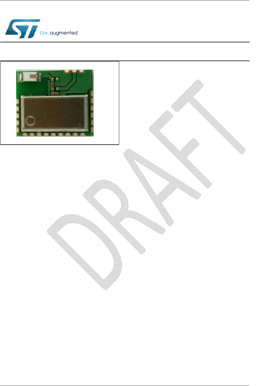
Description
The SPBTLE-1S is a Bluetooth
®
Smart
application processor certified module, compliant
with BT specifications v4.2 and BQE qualified.
The SPBTLE-1S module supports multiple roles
simultaneously and can act at the same time as
Bluetooth Smart master and slave device.
The SPBTLE-1S is based on BlueNRG-1 system-
on-chip and entire Bluetooth Low Energy stack
and protocols are embedded into module.
The SPBTLE-1S module provides a complete RF
platform in a tiny form factor. Radio, antenna and
high frequency oscillators are integrated to offer
a certified solution to optimize the time to market
of the final applications.
The SPBTLE-1S can be powered directly with a
pair of AAA batteries or any power source from
1.7 to 3.6 V.
SPBTLE-1S
Features

SPBTLE-1S
Rev 0.1 P a g e | 2
30
Contents
1
General description ................................................................................... 4
2
Block diagram ............................................................................................ 5
3
Software Development .............................................................................. 6
3.1 Software development Kit ............................................................................. 6
3.2 Software Architecture ................................................................................... 6
4
Hardware specifications ........................................................................... 8
4.1 Absolute maximum ratings ........................................................................... 8
4.2 Recommended operating conditions ............................................................ 8
4.3 Current consumption .................................................................................... 8
4.4 Pin assignment ............................................................................................. 9
4.5 Mechanical dimensions .............................................................................. 11
5
Hardware design ......................................................................................12
5.1 Reset Circuitry ............................................................................................ 12
5.2 Debug Interface .......................................................................................... 12
5.3 Reflow soldering ......................................................................................... 13
6
Regulatory compliance ............................................................................15
6.1 FCC certification ......................................................................................... 15
6.1.1
Labeling instructions................................................................................................. 15
6.1.2
Product manual instructions ..................................................................................... 16
6.2 IC certification ............................................................................................ 17
6.2.1
Labeling instructions................................................................................................. 17
6.2.2
Product manual instructions ..................................................................................... 18
6.3 EU Type approval for SPBTLE-1S module ................................................. 19
6.4 Bluetooth certification ................................................................................. 19
7
Ordering information ................................................................................27
8
ECOPACK
®
................................................................................................28

SPBTLE-1S
Rev 0.1 P a g e | 3
30
9
Traceability ...............................................................................................28
10
Revision history .......................................................................................29

SPBTLE-1S
P a g e | 4
Rev. 0.1
1 General description
The SPBTLE-1S is a Bluetooth Smart application processor module compliant with
Bluetooth
®
specifications v4.2 with embedded ceramic antenna.
The SPBTLE-1S module has been designed around the ST BlueNRG-1 SoC where its
Cortex-M0 core can execute both Bluetooth protocols and customer application. A
complete power-optimized Bluetooth stack library provides:
• Master, slave, multiple roles support
• GAP: central, peripheral, observer or broadcaster roles
• simultaneous advertising and scanning
• capability of being slave of up to two masters simultaneously
• ATT/GATT: client and server
• SM: privacy, authentication and authorization
• L2CAP
• Link Layer: AES-128 encryption and decryption
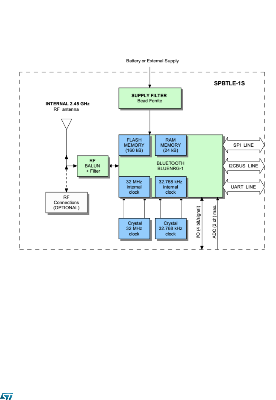
The SPBTLE-1S has 160KB embedded Flash and 24KB embedded RAM memory.
In the module are available 32MHz and 32KHz crystal oscillators. It has been designed to
leverage the BlueNRG-1 integrated DC-DC step down converter.
It can be configured to support Single chip application or Network processor application.
Being based on the BlueNRG-1 SoC, the SPBTLE-1S module leverages all the tools and
documentation of its ecosystem: Development Kit, Application Notes, User Manuals,
Design Notes & Tips. A wide set of sample programs are also available in C source code.
The SPBTLE-1S module has a wide set of peripherals available for customer application (1
x UART interface, 1 x SPI interface, 2 x I
2
C interface, 14 or 15 GPIO, 2 x multifunction
timer, 10-bit ADC, Watchdog & RTC, DMA controller, PDM stream processor).
The SPBTLE-1S module enables wireless connectivity into electronic devices, not requiring
any RF experience or expertise for integration into the final product. The SPBTLE-1S
module provides a complete RF application platform in a tiny form factor (11.5 x 13.5 x 2.0
mm) and being a certified solution optimizes the time to market of the final applications.
The SPBTLE-1S module allows applications to meet the tight advisable peak current
requirements imposed with the use of standard coin cell batteries. Optimized results are
obtained with the embedded high-efficiency DC-DC step-down. SPBTLE-1S can be
powered directly with a standard 3 V coin cell battery, a pair of AAA batteries or any power
source from 1.7 to 3.6 V.
SPBTLE-1S
Rev 0.1 P a g e | 5
30
2 Block diagram
Figure 1: HW block diagram

SPBTLE-1S
P a g e | 6
Rev. 0.1
3 Software Development
3.1 Software development Kit
The SPBTLE-1S module embeds the BlueNRG-1 application processor. Refer to the BlueNRG-1 web
page (http://www.st.com/en/wireless-connectivity/bluenrg-1.html) to get access to:
• BlueNRG-1 datasheet
• development kit
• application notes
• user manuals
• tools & software
• design note and tips
Software and firmware should be configured taking into account the SPBTLE-1 specific configuration as
described in the block diagram chapter. In particular the SPBTLE-1 module has:
• 32 MHz crystal oscillator
• 32 KHz crystal oscillator
• SMPS DC-DC converter
• 10
µ
H SMPS inductor
The projects provided with the development kit should be customized defining as following:
• HS_SPEED_XTAL=HS_SPEED_XTAL_32MHZ
• LS_SOURCE=LS_SOURCE_EXTERNAL_32KHZ
• SMPS_INDUCTOR=SMPS_INDUCTOR_10uH
3.2 Software Architecture
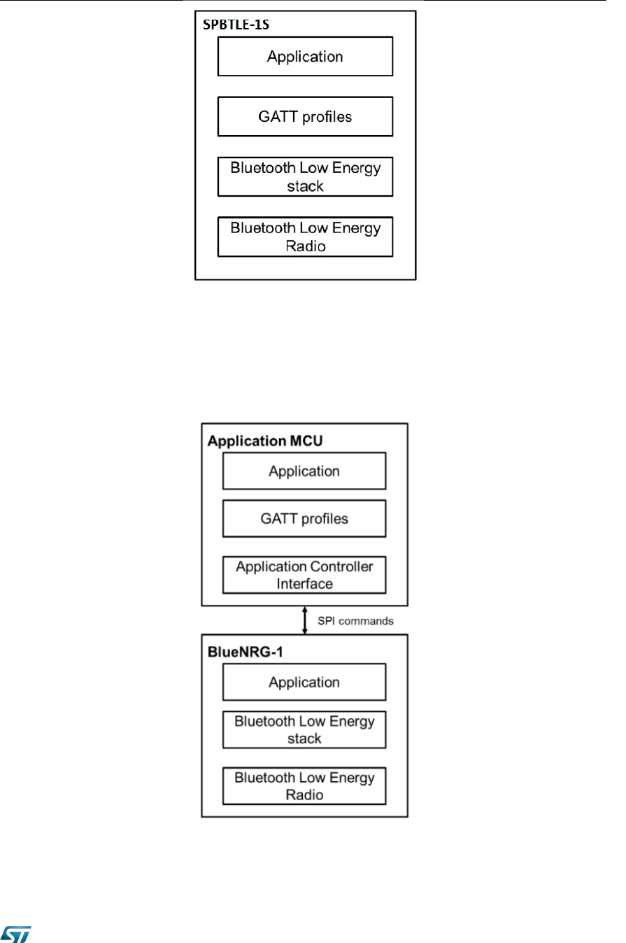
There are two possible software architectures:
1. Host-less mode: customer application runs on the SPBTLE-1S module. Many sample projects
are available in the Development Kit.
SPBTLE-1S
Rev 0.1 P a g e | 7
30
Figure 2: SPBTLE-1S Host less mode
2. Hosted mode: the module is configured as network module controlled by an external host
connected via SPI or UART. A project named DTM is available in the Development Kit that
configures the SPBTLE-1S module as a network module.
Figure 3: Hosted mode
SPBTLE-1S
P a g e | 8
Rev. 0.1
4 Hardware specifications
General conditions (V
IN
= 3.3 V and 25 °C)
4.1 Absolute maximum ratings
Rating
Min
Typ.
Max
Unit
Storage temperature range
-40
-
+85
°C
Supply voltage, V
IN
-0.3
-
3.9
V
I/O pin Voltage (V
IO
five-volt tolerant pin)
-0.3
-
3.9
V
RF saturation input power
-
8
-
dBm
Table 1: Absolute maximum ratings
4.2 Recommended operating conditions
Rating
Min
Typ.
Max
Unit
Storage temperature range
-40
-
+85
°C
Supply voltage, V
IN
1.7
3.3
3.6
V
Signals & I/O pin voltage
(according supply voltage)
1.7
-
3.6
V
RF Frequency
2402
-
2480
MHz
Table 2: Recommended operating conditions
4.3 Current consumption
Characteristics measured over recommended operating conditions unless otherwise
specified. Typical value are referred to T
A
= 25 °C, V
in
= 3.0 V
Symbol
Parameter
Test conditions
Typ.
Unit
IDD
Supply current
Reset
5
nA
Standby
500
nA
Sleep mode
0.9
µA
Active Mode
1.9
mA
RX
7.7
mA
TX: +5dBm
15
mA
TX: 0 dBm 11 mA
Table
3
: Current consumption table
SPBTLE-1S
Rev 0.1 P a g e | 9
30
Current consumption values has been taken using the “BlueNRG current consumption
estimation tool”, configured to match the SPBTLE-1S configuration.
The tool is available on ST.com at:
http://www.st.com/en/embedded-software/stsw-bnrg001.html
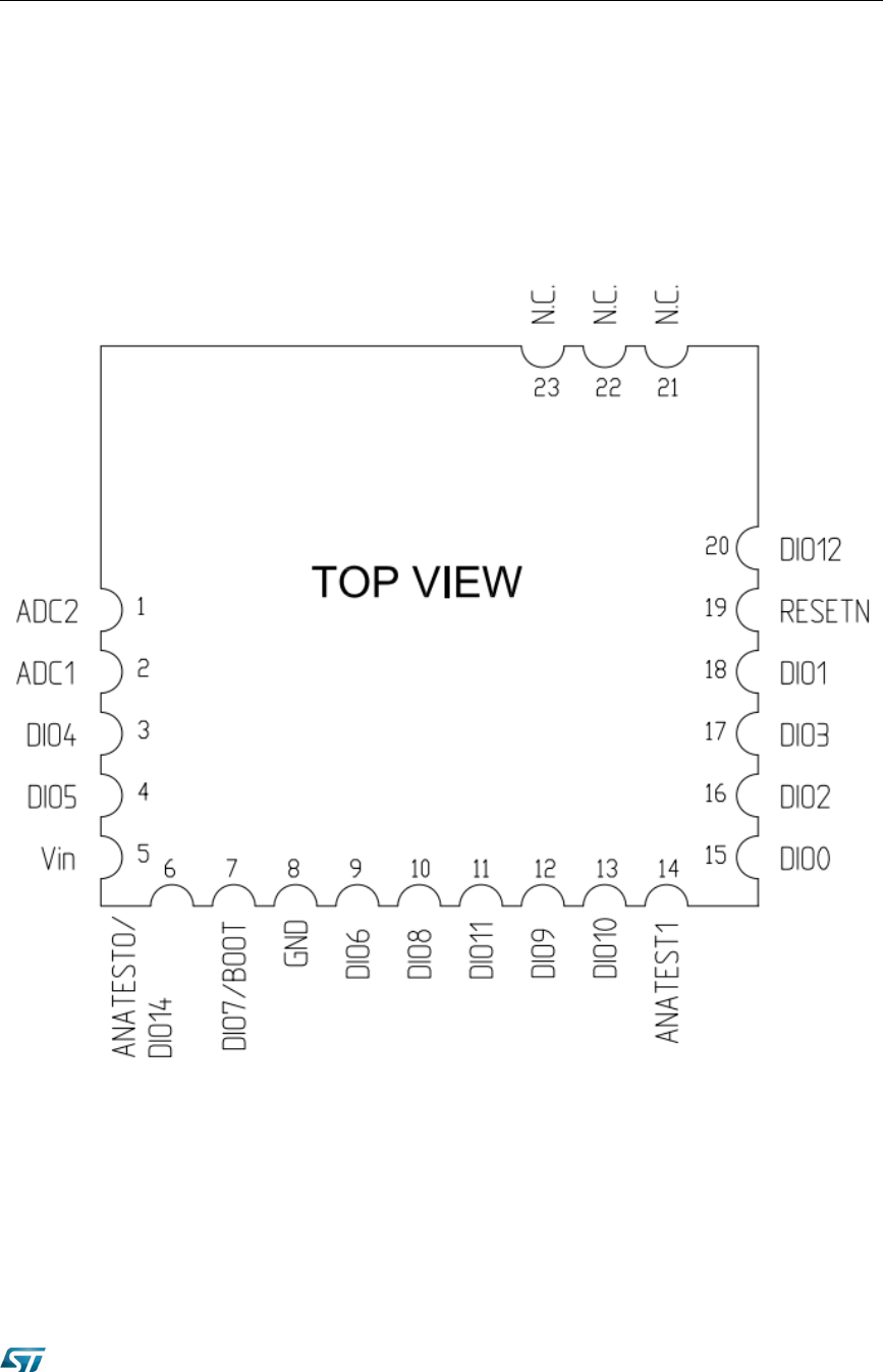
4.4 Pin assignment
Figure 4: Pin connection
SPBTLE-1S
P a g e | 10
Rev. 0.1
Module
Pin #
Module Pin Name
BlueNRG-1 Function
Pin
(CSP package) Mode:
“000” Mode: “001”
Mode:
“100” Mode: “010”
1
ADC2 D5 ADC input 2
2
ADC1 B4 ADC input 1
3
DIO4 C3 GPIO4 UART_RXD
I2C2_CLK PWM0
4
DIO5 C2 GPIO5 UART_TXD
I2C2_DAT PWM1
5
Vin A3, E6 Supply pin
6
ANATEST0/
DIO14/ A5 GPIO14 I2C1_CLK SPI_CLK ADC_DATA
7
DIO7/BOOT(*) D2 GPIO7 UART_CTS
I2C2_DAT PDM_CLK
8
GND A4, B6, C1, F5 Ground
9
DIO6 D1 GPIO6 UART_RTS
I2C2_CLK PDM_DATA
10
DIO8 D3 GPIO8 UART_TXD
SPI_CLK PDM_DATA
11
DIO11 E2 GPIO11 UART_RXD
SPI_CS1 -
12
DIO9 E1 GPIO9 SWCLK SPI_IN
13
DIO10 F1 GPIO10 SWDIO SPI_OUT
14
ANATEST1 D4 Anatest1
15
DIO0 A2 GPIO0 UART_CTS
SPI_CLK -
16
DIO2 A1 GPIO2 PWM0 SPI_OUT PDM_CLK
17
DIO3 B1 GPIO3 PWM1 SPI_IN ADC_CLK
18
DIO1 B2 GPIO1 UART_RTS
SPI_CS1 PDM_DATA
19
RESETN B3 Reset Pin
20
DIO12 F2 GPIO12 - I2C1CLK
21
N.C N/A Must be left floating
22
N.C N/A Must be left floating
23
N.C N/A Must be left floating
Table 4: Pin assignment
(*) The pin DIO7/BOOT is monitored by bootloader after power up or hardware Reset and it should be low to
prevent unwanted bootloader activation
The Table 4 provides the association between SPBTLE-1S module pin and the related BlueNRG-1 pin.
Refer to the BlueNRG-1 datasheet for detailed description.
SPBTLE-1S
Rev 0.1 P a g e | 11
30
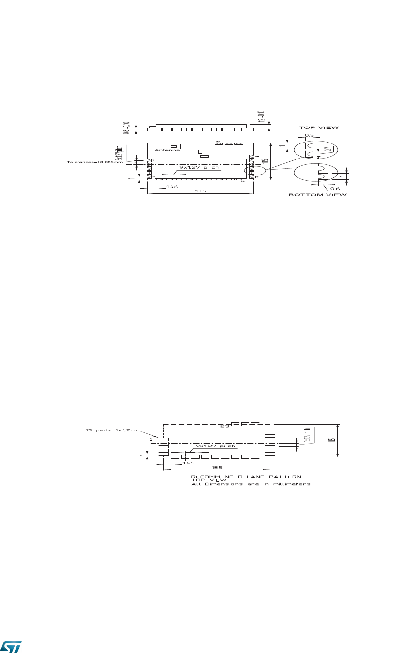
4.5 Mechanical dimensions
Figure 5: Mechanical dimensions
Figure 6: Recommend land pattern top view
SPBTLE-1S
P a g e | 12
Rev. 0.1
5 Hardware design
Note:
-
All unused pins should be left floating; do not ground.
-
GND pin must be well grounded.
-
Traces should not be routed underneath the module.
-
The area around the module should be free of any ground planes, power planes,
trace routings, or metal for 6 mm from the module antenna position, in all directions.
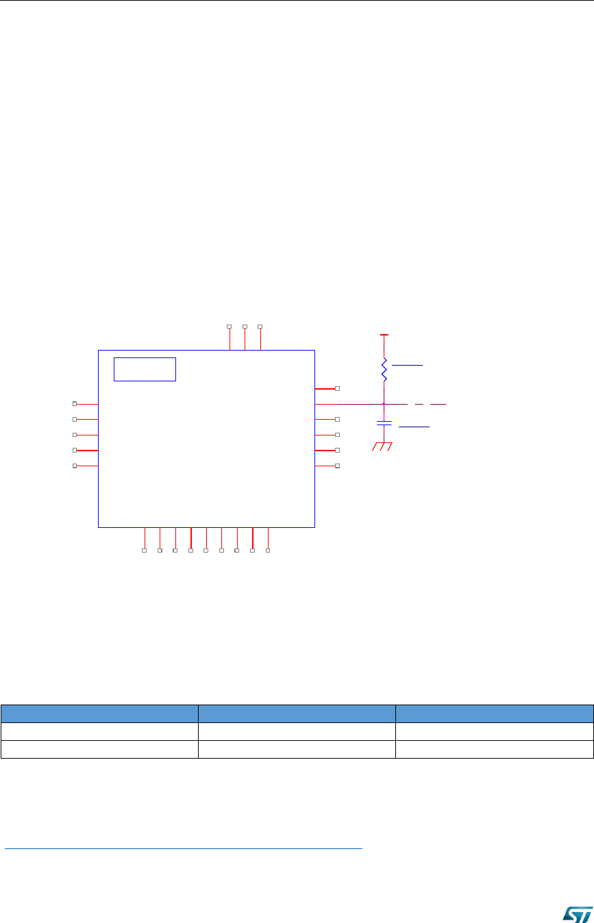
5.1 Reset Circuitry
The SPBTLE-1S module requires an external pull-up reset circuitry to ensure proper operation at power
on. Refer to the “Reset management” chapter of the BlueNRG-1 datasheet for details.
5.2 Debug Interface
The SPBTLE-1S
embeds the ARM serial wire debug (SWD) port. It is two pins (clock and single bi-
directional data) debug interface, providing all the debug functionality plus real time access to system
memory without halting the processor or requiring any target resident code.
Pin Functionality
Module PI
N
Pin description
SWCLK
12
SWD clock signal
SWDIO
13
SWD data signal
Table 5: Debug interface pin
For more information refer to the BlueNRG-1 technical documentation
(http://www.st.com/en/wireless-connectivity/bluenrg-1.html )
ANTENNA
BLE1
SPBTLE-1S MODULE
DIO11
11
DIO6
9
DIO7/BOOT
7
DIO8
10
VBAT
5
GND
8
ANATEST0/DIO14
6
DIO5
4
DIO4
3
ADC1
2
ADC2
1
DIO9
12
DIO10
13
(ANATEST1
14
DIO0 15
DIO2 16
DIO3 17
DIO1 18
RESETN 19
DIO12 20
GND_RF 21
EXT_ANT 22
GND_RF 23
C RESET
10nF
R RESET
47 KOHM
VCC (VBAT)
(IF NEEDED)
TO EXTERNAL CIRCUIT
Figure 7: Reset circuitry
SPBTLE-1S
Rev 0.1 P a g e | 13
30
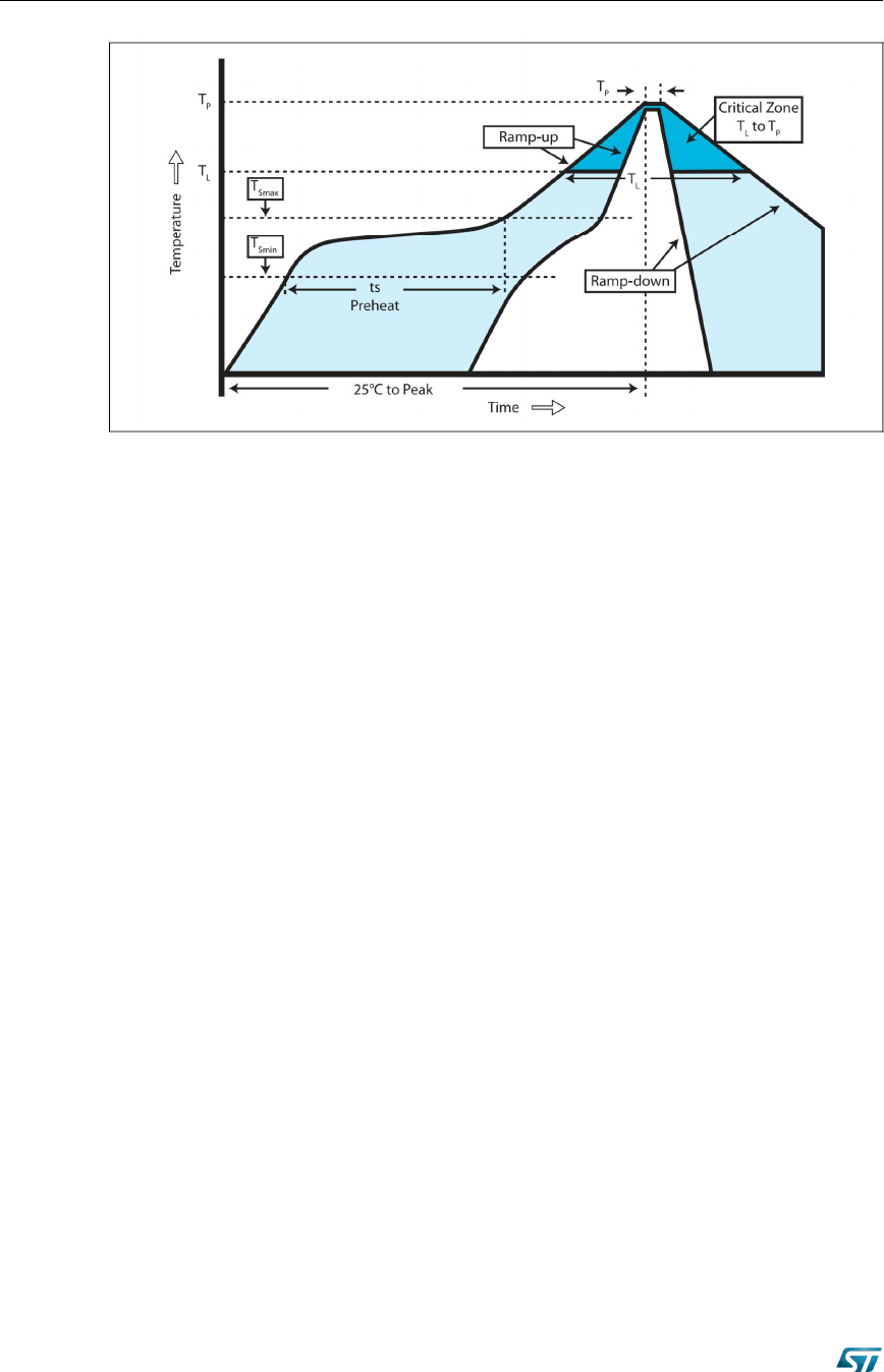
5.3 Reflow soldering
The SPBTLE-1S is a high temperature strength surface mount Bluetooth
®
module supplied
on a 23 pin, 4-layer PCB. The final assembly recommended reflow profiles are indicated
here below.
Soldering phase has to be executed with care: in order to avoid undesired melting
phenomenon, particular attention has to be taken on the set up of the peak temperature.
Here following some suggestions for the temperature profile based on following
recommendations.
Table 6. Soldering
Profile feature
PB-free assembly
Average ramp up rate (T
SMAX
to T
p
)
3°C/ sec max
Preheat
Temperature min (T
S
mn)
Temperature max (T
S
max)
Time (t
S
min to t
S
max) (t
S
)
150 °C
200 °C
60-100 sec
Time maintained above:
Temperature T
L
Time t
L
217 °C
60-70 sec
Peak temperature (T
P
)
240 + 0 °C
Time within 5 °C of actual peak temperature (T
P
)
10-20 sec
Ramp down rate
6 °C/sec
Time from 25 °C to peak temperature
8 minutes max
SPBTLE-1S
P a g e | 14
Rev. 0.1
Figure 8: Soldering profiles

SPBTLE-1S
Rev 0.1 P a g e | 15
30
6 Regulatory compliance
6.1 FCC certification
This module has been tested and found to comply with the FCC part 15 rules. These limits
are designed to provide reasonable protection against harmful interference in approved
installations. This equipment generates, uses, and can radiate radio frequency energy and,
if not installed and used in accordance with the instructions, may cause harmful interference
to radio communications.
However, there is no guarantee that interference may not occur in a particular installation.
This device complies with part 15 of the FCC rules. Operation is subject to the following two
conditions:
1. This device may not cause harmful interference,
and
2. this device must accept any interference received,
including interference that may cause undesired
operation.
Modifications or changes to this equipment not expressly approved by STMicroelectronics
may render void the user's authority to operate this equipment.
Modular approval
FCC ID: S9NSPBTLE1S
In accordance with FCC part 15, the SPBTLE-1S is listed as a modular transmitter device.
This module is evaluated for stand-alone use only. Finished products incorporating multiple
transmitters must comply with colocation and RF exposure requirements in accordance with
FCC multi-transmitter product procedures. Collocated transmitters operating in portable RF
Exposure conditions (e.g. <20 cm from persons including but not limited to body worn and
hand held devices) may require separate approval.
6.1.1 Labeling instructions
When integrating the SPBTLE-1S into the final product, the OEM must ensure that the FCC
labeling requirements are satisfied. A statement must be included on the exterior of the final
product which indicates the product includes a certified module. The label should state the
following (or similar wording that conveys the same meaning):
Contains FCC ID:
S9NSPBTLE1S
OR
This product contains FCC ID:
S9NSPBTLE1S
The OEM must include the following statements on the exterior of the final product unless
the product is too small (e.g. less than 4 x 4 inches):
This device complies with Part 15 of the FCC Rules. Operation is subject to the following
two conditions:

SPBTLE-1S
P a g e | 16
Rev. 0.1
1. this device may not cause harmful interference,
and
2. this device must accept any interference received,
including any interference that may cause
undesired operation.
6.1.2 Product manual instructions
This section applies to OEM final products containing the SPBTLE-1S module, subject to
FCC compliance. The final product manual must contain the following statement (or a
similar statement that conveys the same meaning):
Warning:
Changes or modifications not expressly approved by the
party responsible for compliance could void the user's
authority to operate the equipment. (Part. 15.21)
In the case where an OEM seeks Class B (residential) limits for the final product, the
following statement must be included in the final product manual:
Note: This equipment has been tested and found to comply with the limits for a Class B digital
device, pursuant to part 15 of the FCC Rules. These limits are designed to provide
reasonable protection against harmful interference in a residential installation. This
equipment generates, uses and can radiate radio frequency energy and, if not installed
and used in accordance with the instructions, may cause harmful interference to radio
communications. However, there is no guarantee that interference will not occur in a
particular installation. If this equipment does cause harmful interference to radio or
television reception, which can be determined by turning the equipment off and on, the
user is encouraged to try to correct the interference by one or more of the following
measures:
• Reorient or relocate the receiving antenna.
• Increase the separation between the equipment and receiver.
• Connect the equipment into an outlet on a circuit different from that to which the
receiver is connected.
• Consult the dealer or an experienced radio/TV technician for help.
In the case where an OEM seeks the lesser category of a Class A digital device for the
final product, the following statement must be included in the final product manual:
Note: This equipment has been tested and found to comply with the limits for a Class A digital
device, pursuant to part 15 of the FCC Rules. These limits are designed to provide
reasonable protection against harmful interference when the equipment is operated in a
commercial environment. This equipment generates, uses, and can radiate radio
frequency energy and, if not installed and used in accordance with the instruction manual,
may cause harmful interference to radio communications. Operation of this equipment in a
residential area is likely to cause harmful interference in which case the user will be
required to correct the interference at his expense.

SPBTLE-1S
30
Rev 0.1 P a g e | 17
6.2 IC certification
The SPBTLE-1S module has been tested and found compliant with the IC RSS-210 rules.
These limits are designed to provide reasonable protection against harmful interference in
approved installations. This equipment generates, uses, and can radiate radio frequency
energy and, if not installed and used in accordance with the instructions, may cause harmful
interference to radio communications.
However, there is no guarantee that interference may not occur in a particular installation.
This device complies with RSS-210 of the IC rules. Operation is subject to the following
two conditions:
1. this device may not cause harmful interference, and
2. this device must accept any interference received,
including interference that may cause undesired
operation.
Modifications or changes to this equipment not expressly approved by STMicroelectronics
may render void the user's authority to operate this equipment.
Modular approval
IC: 8976C-SPBTLE1S
In accordance with IC RSS-210, the SPBTLE-1S is listed as a modular transmitter device.
This module is evaluated for stand-alone use only. Finished products incorporating multiple
transmitters must comply with colocation and RF exposure requirements in accordance with
IC multi-transmitter product procedures. Collocated transmitters operating in portable RF
Exposure conditions (e.g. <20cm from persons including but not limited to body worn and
hand held devices) may require separate approval.
6.2.1 Labeling instructions
When integrating the SPBTLE-1S into the final product, the OEM must ensure that the IC
labeling requirements are satisfied. A statement must be included on the exterior of the
final product which indicates that the product includes a certified module. The label should
state the following (or similar wording that conveys the same meaning):
Contains IC: 8976C-SPBTLE1S
OR
This product contains IC: 8976C-SPBTLE1S
The OEM must include the following statements on the exterior of the final product unless
the product is too small (e.g. less than 4 x 4 inches):
This device complies with RSS-210 of the IC Rules. Operation is subject to the following
two conditions:
1. this device may not cause harmful interference, and
2. this device must accept any interference received,
including any interference that may cause
undesired operation.

SPBTLE-1S
P a g e | 18
Rev. 0.1
6.2.2 Product manual instructions
This section applies to OEM final products containing the SPBTLE-1S module, subject to
IC compliance. The final product manual must contain the following statement (or a similar
statement that conveys the same meaning):
Warning: Changes or modifications not expressly approved by the
party responsible for compliance could void the user's
authority to operate the equipment. (RSS-210)
In the case where an OEM seeks Class B (residential) limits for the final product, the
following statement must be included in the final product manual:
Note: This equipment has been tested and found to comply with the limits for a Class B digital
device, pursuant to RSS-210 of the IC Rules. These limits are designed to provide
reasonable protection against harmful interference in a residential installation. This
equipment generates, uses and can radiate radio frequency energy and, if not installed
and used in accordance with the instructions, may cause harmful interference to radio
communications. However, there is no guarantee that interference will not occur in a
particular installation. If this equipment does cause harmful interference to radio or
television reception, which can be determined by turning the equipment off and on, the
user is encouraged to try to correct the interference by one or more of the following
measures:
• Reorient or relocate the receiving antenna.
• Increase the separation between the equipment and receiver.
• Connect the equipment into an outlet on a circuit different from that to which the
receiver is connected.
• Consult the dealer or an experienced radio/TV technician for help.
In the case where an OEM seeks the lesser category of a Class A digital device for the
final product, the following statement must be included in the final product manual:
Note: This equipment has been tested and found to comply with the limits for a Class A digital
device, pursuant to RSS-210 of the IC Rules. These limits are designed to provide
reasonable protection against harmful interference when the equipment is operated in a
commercial environment. This equipment generates, uses, and can radiate radio
frequency energy and, if not installed and used in accordance with the instruction manual,
may cause harmful interference to radio communications. Operation of this equipment in a
residential area is likely to cause harmful interference in which case the user will be
required to correct the interference at his expense.
(Please see APPENDIX A for the French translation)

SPBTLE-1S
30
Rev 0.1 P a g e | 19
6.3 EU Type approval for SPBTLE-1S module
This module complies with the following European EMI/EMC and safety directives and standards:
-
EN 62479:2010
-
EN 60950-1:2006 + A11:2009 + A1:2010 + A12:2011 + A2:2013
-
ETSI EN 301 489-17 V3.1.1 (2017-02)
-
ETSI EN 301 489-1 V2.1.1 (2017-02)
-
ETSI EN 300 328 v 2.1.1 (2016-11)
6.3.1 Labeling instructions
Pending
6.3.2 Product manual instructions
Pending
6.4 Bluetooth certification
The module with embedded stack and profile has been qualified in accordance with SIG
qualification rules:
• Declaration ID: pending
• Qualified design ID: pending
• Product type: End Product
• Core spec version: 4.2
• Product description: Bluetooth Smart v4.2 module

SPBTLE-1S
P a g e | 20
Rev. 0.1
Appendix A
Déclaration de conformité
A.1 Certification FCC
Le module SPBTLE-1S a été testé et déclaré conforme avec la section 15 de la Règlementation
FCC. Ces limitations sont stipulées afin de procurer une protection raisonnable contre les
interférences gênantes dans les installations approuvées.
Cet appareil génère, utilise et diffuse
des ondes radio et, s’il n’est pas installé et utilisé en conformité avec les instructions dont il fait
l’objet, peut causer des interférences gênantes sur les communications radio.
Il n’y a cependant pas de garantie qu’une interférence ne se produira pas dans une installation
particulière.
Cet appareil est en conformité avec la section 15 des règlements FCC. L’utilisation est
soumise aux deux conditions suivantes: (1) cet appareil ne doit pas causer d'interférences
nocives, et (2) Cet appareil doit supporter toute interférence reçue, y compris des interférences
qui peuvent provoquer un fonctionnement non désiré.
Tout changement ou modification fait(e) à cet appareil et non expressément approuvé(e)
par STMicroelectronics peut annuler l’autorisation pour l’utilisateur de faire fonctionner
l’appareil.
Approbation du module
FCC ID: S9NSPBTLE1S
Conformément à la section 15 des règlements FCC, le module SPBTLE-1S est répertorié comme
un dispositif émetteur modulaire.
Ce module n’est évalué que pour une utilisation autonome. Les produits finis incorporant
plusieurs émetteurs doivent être conformes à la colocation et aux exigences d'exposition RF
en concordance avec les procédures FCC multi-émetteurs. D’autres émetteurs fonctionnant
dans des dispositifs portables exposés aux RF (par exemple, situés à moins de 20 cm des
personnes avec dispositifs portatifs ou portés contre le corps) peuvent nécessiter
d'une
approbation séparée.

SPBTLE-1S
30
Rev 0.1 P a g e | 21
A.1.1 Instructions d'étiquetage
Lors de l'intégration du module SPBTLE-1S dans le produit final, le fabricant doit s’assurer
que les exigences en matière d'étiquetage de la FCC sont satisfaites. Une déclaration doit être
placée sur l’étiquette extérieure du produit final indiquant que le produit comprend un module
certifié. L'étiquette doit comporter les informations suivantes (ou une mention analogue que
recouvre la même notion):
Contient FCC ID: S
9NSPBTLE1S
OU Ce produit contient FCC ID: S9NSPBTLE1S
Le sous-traitant doit inclure les énoncés suivants sur l’étiquette extérieure du produit final à
moins que le produit
ne soit trop petit (par exemple moins de 4 x 4 pouces):
Cet appareil est en conformité avec la section 15 des règlements FCC. L’utilisation est
soumise aux deux conditions suivantes:
(1) cet appareil ne doit pas causer d'interférences nocives, et
(2) Cet appareil doit supporter toute interférence reçue, y compris des interférences qui peuvent provoquer un
fonctionnement non désiré.
A.1.2 Instructions pour l’utilisation du produit
La présente section concerne les produits finis contenant le module SPBTLE-1S, assujettis aux
normes FCC. Le manuel du produit final doit contenir la déclaration suivante (ou une mention
analogue que recouvre la même notion):
“
Avertissement: Les changements ou modifications non expressément approuvés par la
partie responsable de la conformité pourraient annuler l'autorisation de l'utilisateur de faire
fonctionner cet équipement. (Section 15.21)”
Dans le cas où le produit finis d’un fabriquant OEM rentre dans les limites de la Classe B
(résidentiel), les énoncés suivants doivent être inclus dans le manuel du produit finis:

SPBTLE-1S
P a g e | 22
Rev. 0.1
“Remarque : Cet équipement a été testé et déclaré conforme aux limitations prévues dans le
cadre de la classe B des appareils numériques, définies par la section 15 du règlement de la
FCC. Ces limites sont conçues pour fournir une protection raisonnable contre toute
interférence dangereuse issue d'une installation résidentielle. Cet équipement produit, utilise
et peut émettre de l'énergie radio électrique et, s'il n'est pas installé et utilisé conformément
aux présentes instructions, peut causer des interférences nuisibles aux communications radio.
Cependant, il se peut que des interférences se produisent dans une installation particulière. Si
cet appareil cause des interférences nuisibles à la réception des signaux de radio ou de
télévision, ce qui peut être déterminé en allumant et en éteignant l'appareil, on encourage
l'utilisateur d'essayer de corriger ces interférences par l'un des moyens suivants:
– Réorienter ou repositionner l'antenne de réception.
– Augmenter la distance séparant l’équipement du récepteur.
– Connecter l’équipement à une prise appartenant à un circuit différent de celui sur
lequel le récepteur est connecté.
– Consulter le revendeur ou un technicien radio/TV expérimenté pour obtenir de l’aide.”
Dans le cas où le produit fini d’un sous-traitant rentre dans les limites imposées aux
appareils numériques de classe A, les énoncés suivants doivent être inclus dans le
manuel du produit finis:
“REMARQUE : Cet appareil a été testé et certifié conforme aux spécifications d'un appareil
électronique de classe A (class A digital device), conformément à la partie 15 du règlement de
la FCC. Ces contraintes sont destinées à fournir une protection raisonnable contre les
interférences nuisibles quand l'appareil est utilisé dans une installation commerciale. Cet
équipement produit, utilise et peut émettre de l'énergie radio électrique et, s'il n'est pas
installé et utilisé conformément aux présentes instructions, peut causer des interférences
nuisibles aux communications radio. L'utilisation de cet appareil dans une installation
résidentielle peut entraîner des interférences nuisibles et l'utilisateur devra corriger les
interférences à ses propres frais.”

SPBTLE-1S
30
Rev 0.1 P a g e | 23
A.2 Certification IC
(a)
Le module SPBTLE-1S a été testé et déclaré conforme avec la Règlementation IC CNR-210. Ces
limitations sont stipulées afin de procurer une protection raisonnable contre les
interférences gênantes en installations approuvées. Cet appareil génère, utilise et diffuse des
ondes radio et, s’il n’est pas installé et utilisé en conformité avec les instructions dont il fait
l’objet, peut causer des interférences gênantes sur les communications radio.
Il n’y a cependant pas de garantie qu’une interférence ne se produira pas dans une installation
particulière.
Ce produit répond aux exigences de la norme CNR-210 d'Industrie Canada. Son
fonctionnement est soumis aux deux conditions suivantes:
(1) cet appareil ne doit pas causer d'interférences nocives, et
(2) Cet appareil doit supporter toute interférence reçue, y compris des interférences qui
peuvent provoquer un fonctionnement non désiré.
Tout changement ou modification fait(e) à cet appareil et non expressément approuvé(e)
par STMicroelectronics peut annuler l’autorisation pour l’utilisateur de faire fonctionner
l’appareil.
Approbation du module
IC: 8976C-SPBTLE1S
Conformément à IC CNR-210, le module SPBTLE-1S est répertorié comme un dispositif émetteur
modulaire
Ce module n’est évalué que pour une utilisation autonome. Les produits finis incorporant
plusieurs émetteurs doivent être conformes à la colocation et aux exigences d'exposition RF
en concordance avec les procédures FCC multi-émetteurs. D’autres émetteurs fonctionnant
dans des dispositifs portables exposés aux RF (par exemple, situés à moins de 20 cm des
personnes avec dispositifs portatifs ou portés contre le corps) peuvent nécessiter
d'une
approbation séparée.
A.2.1 Instructions d'étiquetage
Lors de l'intégration du module SPBTLE-1S dans le produit final, le fabricant doit s’assurer que
les exigences en matière d'étiquetage de la IC sont satisfaites. Une déclaration doit être placée
sur l’étiquette extérieure du produit final indiquant que le produit comprend un module certifié.

SPBTLE-1S
P a g e | 24
Rev. 0.1
L'étiquette doit comporter les informations suivantes (ou une mention analogue que recouvre
la même notion):
Contient IC ID: 8976C-SPBTLE1S
OU Ce produit contient IC ID: 8976C-SPBTLE1S
Le sous-traitant doit inclure les énoncés suivants sur l’étiquette extérieure du produit final à
moins que le produit
ne soit trop petit (par exemple moins de 4 x 4 pouces):
Cet appareil est en conformité aux normes IC. L’utilisation est soumise aux deux conditions
suivantes:
(1) cet appareil ne doit pas causer d'interférences nocives, et
(2) Cet appareil doit supporter toute interférence reçue, y compris des interférences qui
peuvent provoquer un fonctionnement non désiré
A.2.2 Instructions pour l’utilisation du produit
La présente section concerne les produits finis contenant le module SPBTLE-1S, assujettis aux
normes IC. Le manuel du produit final doit contenir la déclaration suivante (ou une mention
analogue que recouvre la même notion):
“Avertissement: Les changements ou modifications non expressément approuvés par la
partie responsable de la conformité pourraient annuler l'autorisation de l'utilisateur de faire
fonctionner cet équipement. (CNR-210)”
Dans le cas où le produit finis d’un fabriquant OEM rentre dans les limites de la Classe B
(résidentiel), les énoncés suivants doivent être inclus dans le manuel du produit finis:
“ Remarque : Cet équipement a été testé et déclaré conforme aux limitations prévues dans le
cadre de la classe B des appareils numériques, définies par la norme CNR-210 d'Industrie
Canada.

SPBTLE-1S
30
Rev 0.1 P a g e | 25
Ces limites sont conçues pour fournir une protection raisonnable contre toute interférence
dangereuse issue d'une installation résidentielle. Cet équipement produit, utilise et peut
émettre de l'énergie radio électrique et, s'il n'est pas installé et utilisé conformément aux
présentes instructions, peut causer des interférences nuisibles aux communications radio.
Cependant, il se peut que des interférences se produisent dans une installation particulière. Si
cet appareil cause des interférences nuisibles à la réception des signaux de radio ou de
télévision, ce qui peut être déterminé en allumant et en éteignant l'appareil, nous
encourageons l'utilisateur à essayer de corriger ces interférences par l'un des moyens suivants:
– Réorienter ou repositionner l'antenne de réception.
– Augmenter la distance séparant l’équipement du récepteur.
– Connecter l’équipement à une prise appartenant à un circuit différent de celui sur
lequel le récepteur est connecté.
– Consulter le revendeur ou un technicien radio/TV expérimenté pour obtenir de l’aide.”
Dans le cas où le produit finis d’un fabriquant OEM rentre dans le cadre des limites imposées
aux appareils numériques de classe A, les énoncés suivants doivent être inclus dans le manuel
du produit finis:
“ REMARQUE: Cet appareil a été testé et certifié conforme aux spécifications d'un appareil
électronique de classe A (class A digital device), conformément à la norme CNR-210 d'Industrie
Canada. Ces contraintes sont destinées à fournir une protection raisonnable contre les
interférences nuisibles quand l'appareil est utilisé dans une installation commerciale. Cet
équipement produit, utilise et peut émettre de l'énergie radio électrique et, s'il n'est pas
installé et utilisé conformément aux présentes instructions, peut causer des interférences
nuisibles aux communications radio. L'utilisation de cet appareil dans une installation
résidentielle peut entraîner des interférences nuisibles et l'utilisateur devra corriger les
interférences à ses propres frais.”
SPBTLE-1S
P a g e | 26
Rev. 0.1
A.3 Certification CE
Le module SPBTLE-1S a obtenu une certification de conformité aux normes suivantes:-
-
EN 62479:2010
-
EN 60950-1:2006 + A11:2009 + A1:2010 + A12:2011 + A2:2013
-
ETSI EN 301 489-17 V3.1.1 (2017-02)
-
ETSI EN 301 489-1 V2.1.1 (2017-02)
-
ETSI EN 300 328 v 2.1.1 (2016-11)
Le module est certifié CE:

SPBTLE-1SS
30
Rev 0.1 P a g e | 27
7 Ordering information
Order code
Description
Packing
MOQ
SPBTLE-1S
Bluetooth
®
V4.2 smart module
TBD
TBD
Figure 9: Ordering information
SPBTLE-1S
30
Rev 0.1 P a g e | 28
8 ECOPACK
®
In order to meet environmental requirements, ST offers these devices in different grades of
ECOPACK
®
packages, depending on their level of environmental compliance. ECOPACK
®
specifications, grade definitions and product status are available at: www.st.com.
ECOPACK
®
is an ST trademark.
9 Traceability
Each module is univocally identified by serial number stored in a 2D data matrix laser
marked on the bottom side of the module itself.
The serial number has the following format:
Letter
Meaning
WW
Week
YY
Year
D
Product ID family
FF
Production panel coordinate identification
NNN
Progressive serial number.
Figure 10: Traceability information
Each module bulk is identified by a bulk ID.
BULK ID and module 2D data matrix are linked by a reciprocal traceability link.
The module 2D data matrix traces the lot number of any raw material used.

SPBTLE-1S
Rev 0.1 P a g e | 29
30
10 Revision history
Date
Revision
Changes
02-Feb-2017
1
Initial release.
15-Feb-2017 2 Pinout updated. Certification updated. Minor updates.
Figure 11: Document revision history

SPBTLE-1S
P a g e | 30
Rev. 0.1
IMPORTANT NOTICE – PLEASE READ CAREFULLY
STMicroelectronics NV and its subsidiaries (“ST”) reserve the right to make changes, corrections, enhancements, modifications, and
improvements to ST products and/or to this document at any time without notice. Purchasers should obtain the latest relevant information
on ST products before placing orders. ST products are sold pursuant to ST’s terms and conditions of sale in place at the time of order
acknowledgement.
Purchasers are solely responsible for the choice, selection, and use of ST products and ST assumes no liability for application assistance or
the design of Purchasers’ products.
No license, express or implied, to any intellectual property right is granted by ST herein.
Resale of ST products with provisions different from the information set forth herein shall void any warranty granted by ST for such product.
ST and the ST logo are trademarks of ST. All other product or service names are the property of their respective owners.
Information in this document supersedes and replaces information previously supplied in any prior versions of this document.
© 2016 STMicroelectronics – All rights reserved