STL POM0001 2.4GHz Transceiver Module User Manual
STL International Ltd. 2.4GHz Transceiver Module Users Manual
STL >
Users Manual
STL 2.4G transceiver module
Technical Manual
General
-----------
The modules is a low power radio frequency module operating within the ISM 2.4 GHz frequency
band. The radio transceiver is compatible with IEEE.802.15.4 standard with hardware acceleration for
both the IEEE 802.15.4 MAC and AES security.. It also incoproates a 32-bit ARM7 core based MCU, 128
Kbyte FLASH memory and 96 Kbyte RAM. It is intended for use as a short range radio module
for embedded applications.
Features Summary
- IEEE 802.15.4 standard compliant on-chip transceiver/modem
- 2.4 GHz ISM Band operation
- Programmable transmitter output power (-30 dBm to +4 dBm typical)
- World-class receiver sensitivity
-96 dBm typical receiver sensitivity using DCD mode (<1% PER, 20-byte packets)
-100 dBm typical receiver sensitivity using NCD mode (<1% PER, 20-byte packets)
Hardware acceleration for IEEE 802.15.4 applications
MAC accelerator (sequencer and DMA interface)
Advanced encryption/decryption hardware engine (AES 128-bit)
Supports standard IEEE 802.15.4 signaling with 250 kbps data rate
32-bit ARM7TDMI-S CPU core with programmable performance up to 26 MHz (24 MHz typical)
Extensive on-board memory resources
— 128 Kbyte serial FLASH memory (will be mirrored into RAM)
— 96 Kbyte SRAM
— 80 Kbyte ROM
built in voltage regulator
UART and SPI interface for control and data interface
GPIOs for general control
RF Shield can to reduce interference
3.3V DC supply
CONFIDENTIAL
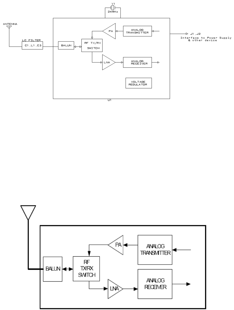
Block Diagram
Fig. 1 Block Diagram
RF Operation
The RF radio interface provides for low cost and the high density as shown in Figure 2. The
transceiver is a zero IF radio without intermediate frequency (IF)stage. An onboard balun along
with a TX/RX switch allows direct connection to a single-ended 50-Ω antenna. The integrated PA
provides programmable output power typically from -30 dBm to +4 dBm, and the RX LNA
provides -96 dBm sensitivity. In addition, separate complementary PA outputs allow use of an
external PA and/or an external LNA for extended range applications. The device also has onboard
bypass capacitors and crystal load capacitors for the smallest footprint in the industry. All
components are integrated into the package except the crystal and antenna.
Figure 2. MC13224V RF Radio Interface
Refer to Freescale MC13224V datasheet for details.
Pin Assignements
J1
Pin No. Name Direction
1 UART1_RTS input
2 UART1_CTS output
3 UART1_RX input
4 UART1_TX output
5 KPI_3 input/output
6 KPI_4 input/output
7 KPI_5 input/output
J2
1 VCC power
2 GND ground
3 SPI_SS input
4 SPI_MISO output
5 SPI_MOSI input
6 SPI_CLK output
Fig. 3 Connectors and Pin Assignments
J2
J1
Pin1 Pin 1
Electrical Specification
DC
1.Supply voltage: 2.0V – 3.6V
2.Off current: <= 1ma
3.standby current <=20 ma
4.Transmit current <= 40 ma
5.Receive current <= 30ma
Receiver
1. Frequency : 2.420 GHz
2. Sensitivity for 1% Packet Error Rate (PER) :
Non-coherent Differential Chip Detection (DCD) Typical -96 dBm
Non-coherent Detection (NCD) Typical -100 dBm
3. Saturation (maximum input level) : Typical 10 dBm
4. Channel Rejection for 1% PER (desired signal -82 dBm)
+5 MHz (adjacent channel) Typical 38 dB
-5 MHz (adjacent channel) Typical 38 dB
+10 MHz (alternate channel) Typical 57 dB
-10 MHz (alternate channel) Typical 57 dB
>= 15 MHz Typical 65 dB
5. Frequency Error Tolerance : Typical 300 kHz
Transmitter
1. Frequency : 2.420 GHz
2. Nominal Output Power : -2 to +4.5 dBm
3. Error Vector Magnitude
Pout @ -30 dBm : Typical 13%
Pout @ 0 dBm : Typical 11%
Pout @ +4 dBm : Typical 9 %
4. Output Power Control Range : Typical 35 dB

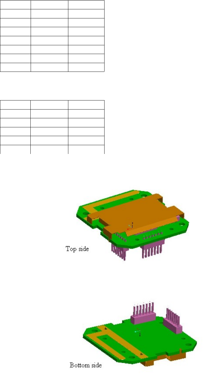
Mechanical drawing
Fig. 4 Mechanical Dimensions
Installation Guide
1.The module can be mounted to the target product using a socket
without soldering.
2.Please follow the pin assignments to connect the module to the
socket on the target product.
3.Make sure that the specified supply voltage is not exceeded.
4.Make usre that the supply voltage is clean from noise and ripple.
5.Decoupling capacitor is recommended to be placed next to the
Vcc pin.
6.Unused pins should be disconnected.
7.The module is self sufficient to function without the need for
external components.
8.PCB traces for Vcc and Ground should be thick and short.
9.Make sure there is no metallic object placed directly on top and
below the module after the module is installed.
Important notes to third party user for 2.4G transceiver module
The 2.4G transceiver Module complies with Part 15 of the FCC rules and regulations. Compliance
with the labeling requirements, FCC notices and antenna usage guidelines is required. To fulfill
FCC Certification, the third party user must comply with the following regulations:
1.The third party user must ensure that the text on the external label provided with this device is
placed on the outside of the final product.
Contains FCC ID: RF7POM0001 The enclosed device complies with Part 15 of the FCC Rules.
Operation is subject to the following two conditions: (i.) this device may not cause harmful
interference and (ii.) this device must accept any interference received, including interference
that may cause undesired operation.
2.The 2.4G transceiver Module may only be used with the onboard PCB antenna that have been
tested and approved for use with this module .
3. The 2.4G transceiver Module have been certified by the FCC for use with other products
without any further certification (as per FCC section 2.1091). Modifications not approved by STL
could void the user's authority to operate the equipment.
4.Third party users must test final product to comply with unintentional radiators (FCC section
15.107 & 15.109) before declaring compliance of their final product to Part 15 of the FCC Rules.