Sagem Wireless 95V3 GSM 850/900/1800/1900 MHz Module User Manual
Sagem Wireless GSM 850/900/1800/1900 MHz Module
OEM Instruction Manual

SCT TMO MASV3 SPEC 030 I spec
agrément Quadband.doc
Document . All rights of reproduction and disclosure reserved.
This document contains information on a product under development. SAGEM reserves the right to change or discontinue this
product without notice.
Unit of Saint Christophe
TMO
+$5':$5(
0$69
&24XDGEDQG
Réf. : SCT TMO MASV3 SPEC 30
Revision: I
Réf. sec. : 2x xxx xxx – x
Date : 02/11/04
Page 1 sur 48
&2VSHFLILFDWLRQ
Type of document :
SPECIFICATIONS

Document . All rights of reproduction and disclosure reserved.
This document contains information on a product under development. SAGEM reserves the right to change or discontinue this product
without notice.
&RQFOXVLRQRUVXPPDU\:
This document gives an overview of the CO230 module: a miniature, single-side, BGA board, quad-band
GSM/GPRS module, ready for integration in mobile application like vehicle-mounted or vending machines …
It describes the main functionalities of this module as well as the electrical interfaces, the mechanical
specification (dimension, form…) and the electrical specification of the module.
+$5':$5(
&2VSHFLILFDWLRQ
)RUPRELOHDSSOLFDWLRQV
Ref. : SCT TMO MASV3 SPEC 30 Rev : I 02/11/04
Ref. Sec.
: 2x xxx xxx – x
Réf. : SCT TMO MASV3 SPEC 30
Rev. : H
Réf. sec. : 2x xxx xxx – x
Date : 14/09/04
Document . All rights of reproduction and disclosure reserved. Page 1
This document contains information on a product under development. SAGEM reserves the right to change or discontinue this product without
notice.
&2
*60*35648$'%$1'%&(02'8/(
)2502%,/($33/,&$7,216
Réf. : SCT TMO MASV3 SPEC 30
Rev. : H
Réf. sec. : 2x xxx xxx – x
Date : 14/09/04
Document . All rights of reproduction and disclosure reserved. Page 2
This document contains information on a product under development. SAGEM reserves the right to change or discontinue this product without
notice.
&+$1*(+,6725<
5HY 'DWH 5HDVRQIRUFKDQJH
A 12/07/03 First document
B 15/07/03
LCD addressable, electrical specification, vibrating device interface
description, LED interface, audio interface, keyboard interface
modification, melody chip interface description, Blue tooth interface
description
C 07/10/03 Pinout modification, electrical specification, LED and backlight capability
D 14/11/03 Pinout Modification, LCD and Keyboard Backlight suppression
E 27/01/04 Charge precision, VBAT limitation, OEMEM* signal
F 06/04/04 End of preliminary specification
G 07/05/04 Power consumption
H
I
14/09/04
02/11/04
Pull up / Pull down, certification clarifications
certification clarifications
7$%/(2)&217(176
6&23(
,QWURGXFWLRQ
5HIHUHQFH
6WDQGDUGVFRPSOLDQFH
FRPSOLDQFHZLWKIFFJXLGHOLQHV
7HUPVDQGDEEUHYLDWLRQ
3URGXFWIHDWXUHV
%/2&',$*5$0
)81&7,21$/'(6&5,37,21
6,0
$XGLR
'LVSOD\
3.3.1 Serial interface ........................................................................................................................... 13
3.3.2 Parallel interface to LCD ............................................................................................................ 14
'DWD
3.4.1 Data services.............................................................................................................................. 15
3.4.2 IrDA ............................................................................................................................................ 15
3.4.3 UART 2....................................................................................................................................... 15
3.4.4 V24 ............................................................................................................................................. 15
3.4.5 USB ............................................................................................................................................ 16
$QWHQQD
.H\SDG
9LGHRVHQVRU
3.7.1 I2C interface............................................................................................................................... 17
3.7.2 Parallel interface to sensor......................................................................................................... 17

Réf. : SCT TMO MASV3 SPEC 30
Rev. : H
Réf. sec. : 2x xxx xxx – x
Date : 14/09/04
Document . All rights of reproduction and disclosure reserved. Page 3
This document contains information on a product under development. SAGEM reserves the right to change or discontinue this product without
notice.
([WHUQDOFRPSDQLRQFKLSLQWHUIDFH
3.8.1 I2S interface ............................................................................................................................... 17
3.8.2 Parallel interface to companion chip .......................................................................................... 17
%OXHWRRWKRSWLRQDO
3.9.1 MCSI interface............................................................................................................................ 21
3.9.2 UART interface........................................................................................................................... 22
3.9.3 Clock........................................................................................................................................... 22
0HORG\JHQHUDWLRQ
'$,
&ORFNV
3RZHUPDQDJHPHQWDQGFKDUJH
3.13.1 Battery ........................................................................................................................................ 22
3.13.2 VRIO........................................................................................................................................... 23
3.13.3 Vbackup ..................................................................................................................................... 23
3.13.4 Charge........................................................................................................................................ 23
$FFHVVRULHV
3.14.1 Flap............................................................................................................................................. 23
3.14.2 Network LED .............................................................................................................................. 23
3.14.3 Vibrating device.......................................................................................................................... 24
23(5$7,1*02'(6
0RGHVGHVFULSWLRQ
4.1.1 No supply ................................................................................................................................... 25
4.1.2 OFF ............................................................................................................................................ 25
4.1.3 Active.......................................................................................................................................... 25
4.1.4 Standby ...................................................................................................................................... 25
7UDQVLWLRQVGHVFULSWLRQ
4.2.1 Power_on ................................................................................................................................... 25
4.2.2 Power_off ................................................................................................................................... 26
4.2.3 Switch_on................................................................................................................................... 26
4.2.4 Switch_off................................................................................................................................... 26
4.2.5 Wake up ..................................................................................................................................... 26
%$//287
(/(&75,&$/63(&,),&$7,21
9%$7
95,2
'$,LQWHUIDFH
1HWZRUN/('
6HULDOLQWHUIDFHIRU/&'
.H\ERDUGLQWHUIDFH
9LEUDWLQJGHYLFHFRQWURO
9
,5'$DQG8$57
5HVHW
6SDUH,2
&ORFNV
3DUDOOHOLQWHUIDFHIRUFRPSDQLRQFKLS
3DUDOOHOLQWHUIDFHIRU/&'
86%LQWHUIDFH
00&LQWHUIDFH
9LGHRVHQVRULQWHUIDFH
0&6,LQWHUIDFH
,6LQWHUIDFH
,&LQWHUIDFH
-7$*LQWHUIDFH
$'&
,QWHUUXSWV

Réf. : SCT TMO MASV3 SPEC 30
Rev. : H
Réf. sec. : 2x xxx xxx – x
Date : 14/09/04
Document . All rights of reproduction and disclosure reserved. Page 4
This document contains information on a product under development. SAGEM reserves the right to change or discontinue this product without
notice.
9%$&.83
(19,5210(17$/63(&,),&$7,21
2SHUDWLQJFRQGLWLRQV
&OLPDWLFFRQGLWLRQV
0(&+$1,&$/63(&,),&$7,21
$11(;(

Réf. : SCT TMO MASV3 SPEC 30
Rev. : H
Réf. sec. : 2x xxx xxx – x
Date : 12/05/04
DRAFT
Document . All rights of reproduction and disclosure reserved. Page 5
This document contains information on a product under development. SAGEM reserves the right to change or discontinue this product
without notice.
6&23(
,1752'8&7,21
This document gives an overview of the CO230 module: a miniature, single-side, BGA board, quad-band
GSM/GPRS module, ready for integration in mobile application like vehicle-mounted or vending machines…
It describes the main functionalities (GPRS / GSM 850MHz / GSM 900MHz / DCS 1800MHz / PCS
1900MHz, interface to a melody chip, LCD interface, SIM interface, vibrating device interface, audio
interfaces for speaker/microphone or accessories, battery interface, battery charging interface, USB
interface, SD card interface, Sensor interface …) of this module as well as the electrical interfaces, the
mechanical specification (dimension, form…) and the electrical specification of the module.
5()(5(1&(
67$1'$5'6&203/,$1&(
• GSM 02.60: "Digital cellular telecommunications system (Phase 2+); Stage 1 Service Description of the
General Packet Radio Service (GPRS)". Version 6.3.0.
• GSM 03.03: "Digital cellular telecommunications system (Phase 2+); Numbering, addressing and
identification". Version 6.6.0.
• GSM 03.13: "Digital cellular telecommunications system (Phase 2+); Discontinuous Reception (DRX) in
the GSM system". Version 6.0.0.
• GSM 03.60: "Digital cellular telecommunications system (Phase 2+); General Packet Radio Service
(GPRS); Service description; Stage 2". Version 6.7.0.
• GSM 03.64: "Digital cellular telecommunications system (Phase 2+); General Packet Radio Service
(GPRS);Overall description of GPRS radio Interface; Stage 2". Version 6.4.0.
• GSM 04.02: "Digital cellular telecommunications system (Phase 2+); GSM Public Land Mobile Network
(PLMN) access reference configuration". Version 6.0.0.
• GSM 04.03: "Digital cellular telecommunications system (Phase 2+); Mobile Station - Base Station
System (MS - BSS) interface Channel structures and access capabilities". Version 6.0.0.
• GSM 04.04: "Digital cellular telecommunications system (Phase 2+); Layer 1 General requirements".
Version 6.0.0.
• GSM 04.05: "Digital cellular telecommunications system (Phase 2+); Data Link (DL) layer General
aspects". Version 6.0.1.
• GSM 04.07: "Digital cellular telecommunications system (Phase 2+); Mobile radio interface signalling
layer 3 General aspects". Version 6.5.1.
• GSM 04.08: "Digital cellular telecommunications system (Phase 2+);Mobile radio interface layer 3
specification". Version 6.11.0.
• GSM 04.60: "Digital cellular telecommunications system (Phase 2+); General Packet Radio Service
(GPRS); Radio Link Control/Medium Access Control (RLC/MAC) protocol". Version 6.9.0.
• GSM 04.64: "Digital cellular telecommunications system (Phase 2+); General Packet Radio Service
(GPRS); Logical Link Control (LLC)". Version 6.7.0.
• GSM 04.65: : "Digital cellular telecommunications system (Phase 2+); General Packet Radio Service
(GPRS); Mobile Station (MS) - Serving GPRS Support Node (SGSN); Sub network Dependent
Convergence Protocol (SNDCP)". Version 6.7.0.
• GSM 05.02: "Digital cellular telecommunications system (Phase 2+); Multiplexing and multiple access on
the radio path". Version 6.9.0.
• GSM 05.03: "Digital cellular telecommunications system (Phase 2+); Channel coding". Version 6.2.1.
• GSM 05.08: "Digital cellular telecommunications system (Phase 2+); Radio subsystem link control".
Version 6.8.0.

Réf. : SCT TMO MASV3 SPEC 30
Rev. : H
Réf. sec. : 2x xxx xxx – x
Date : 12/05/04
DRAFT
Document . All rights of reproduction and disclosure reserved. Page 6
This document contains information on a product under development. SAGEM reserves the right to change or discontinue this product
without notice.
• GSM 05.10: "Digital cellular telecommunications system (Phase 2+); Radio subsystem synchronisation".
Version 6.6.0.
• GCF-CC (V.3.12.0) and GT.01.
• NAPRD.03 (V.2.10.1).
&203/,$1&(:,7+)&&*8,'(/,1(6
Fix-mount and mobile devices incorporating CO230 modules must be designed to maintain a minimum
separation distance of 20 cm between the antenna and the end user to satisfy RF exposure requirements for
mobile transmitting devices.
7(506$1'$%%5(9,$7,21
ADC Analog to Digital Converter
ADPCM Adaptive Delta Pulse Code Modulation
AFC Application Frequency Correction
ASIC Application Specific Integrated Circuit
BMP Bitmap
CODEC Coder-Decoder
CTS Clear To Send
DAC Digital to Analog Converter
DAI Digital Analog Interface
DCS Digital
DSP Data Signal Processor
DSR Data Set Ready
DTR Data Terminal Ready
EGSM Enhanced GSM
EMS Enhanced Messaging Services
ESD Electrostatic Discharge
ETS European Telecommunication Standard
GSM Global Standard for Mobile communication
GPRS Global Packet Radio Services
IC Integrated Circuit
IEEE Institute of Electrical and Electronics Engineers
I/O Input / Output
IRDA Infra Red
ISO International Standards Organisation
ITU International Telecommunication Union
JPEG Joint Picture Expert Group
JTAG Joint Test Action Group
KBPS Kbit per second
LCD Liquid Crystal Display
LED Diode
LNA Low Noise Amplifier
MBPS Mbit per second
MIDI Musical Instrument Digital Interface
MMI Man Machine interface
PA Power Amplifier
PBCCH Packet Broadcast Channel
PCB Printed Circuit Board
PCS Personal Communication System
PLL Phase Locked Loop
PNG Portable Network Graphics
RAM Random Access Memory
RF Radio Frequency
RI Ring Indication
Réf. : SCT TMO MASV3 SPEC 30
Rev. : H
Réf. sec. : 2x xxx xxx – x
Date : 12/05/04
DRAFT
Document . All rights of reproduction and disclosure reserved. Page 7
This document contains information on a product under development. SAGEM reserves the right to change or discontinue this product
without notice.
RMS Root Mean Square
RTS Ready To Send
RX Receive direction
SIM Subscriber Identification Module
SMS Short Message Service
SRAM Static Random Access Memory
TBC To Be Confirmed
TBD To Be Defined
TX Transmit direction
UART Universal Asynchronous Receiver and Transmitter
USB Universal Serial Bus
USSD Unstructured Supplementary Service Data
VCO Voltage Controlled Oscillator
WAP Wireless Application Protocol
WBMP Wide Bitmap
352'8&7)($785(6
Temperature range
Normal range: -10°C to +55°C (fully compliant)
Extended range: -20°C to –10°C and +55°C to +70°C
(functional without any risk for the network)
Storage: -40°C to °85°C
Weight (in g) 10g
ESD ESD protected, < 1kv or 2kv (see application note)
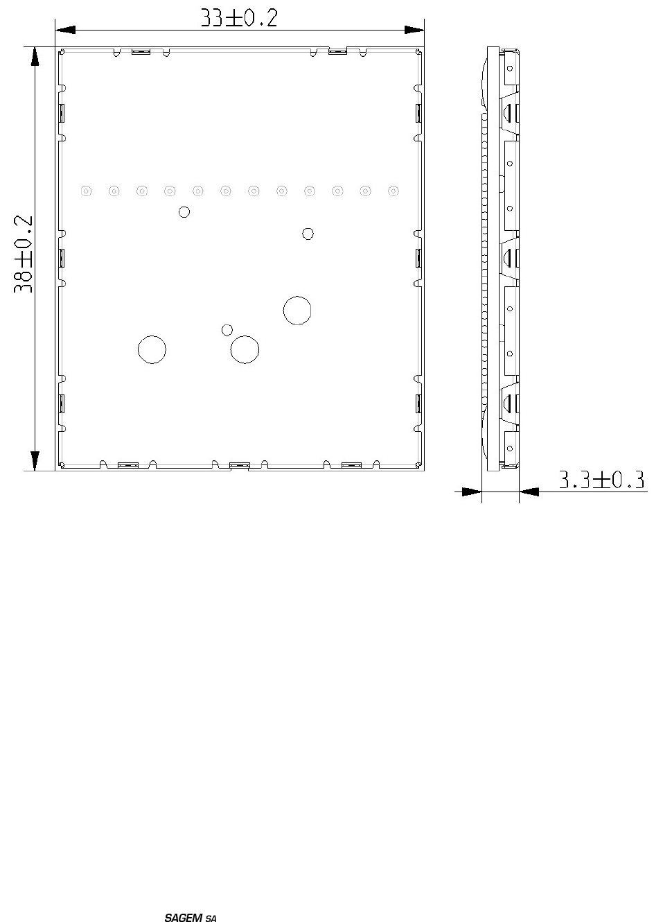
Physical dimensions 33x38x3.3 mm (typical)
Connection BGA type connection (including antenna and battery
connection)
Power supply 3.45V to 4.5V range, 3.8V nominal.
Power consumption
Off mode: 80uA (typ)
Standby mode: 2mA (typ)
Communication mode: 260mA (GSM/DCS à Pmax)
2.2A (GSM peak during TX
slot)
Battery charge management and interface
Battery charge management is included for regulated
charger to 600mA maximum charge current.
Specific un-regulated charger qualified by SAGEM
could be used (see application note).
Antenna connection No antenna included in the module. Antenna
connection is included in the BGA ball-out. See
recommendations for connection.
Frequency bands GSM 850MHz + EGSM900 + DCS1800 + PCS1900
Voice codecs Half Rate, Full Rate, Enhanced Full Rate
GSM class Small MS
Transmit power Class 4 (2W) for GSM 850MHz EGSM900
Class 1 (1W) for DCS1800 / PCS1900
Supported SIM card
3V SIM cards.
To prevent SIM card’s damages, the power supply of
the module has to be turned off before any
manipulation of the SIM card.
SIM slot Not included on the module. Signals for the
management of the SIM card are provided on ball-
out.
Vibrating device Not included in the module. Control is provided on
ball-out.

Réf. : SCT TMO MASV3 SPEC 30
Rev. : H
Réf. sec. : 2x xxx xxx – x
Date : 12/05/04
DRAFT
Document . All rights of reproduction and disclosure reserved. Page 8
This document contains information on a product under development. SAGEM reserves the right to change or discontinue this product
without notice.
Keyboard / LCD backlight / network LED (GB) GB LED management. Interface to external backlight
and RGB component.
Audio up-link 2x2 differential inputs are provided for microphone
(accessories and handset).
Audio down-link non stereo 3x2 differential outputs are provided for non stereo
earphone (accessories and 6 ohms and 32 ohms).
Audio down-link stereo 3 outputs are provided for stereo earphone
(accessories and handset).
Flap open/closed detection IO5 dedicated for Flap.
Keyboard interface 6x6 keyboard interface is provided on ball-out.
UART1 interface with flow control
Up to 115.2 Kbaud with auto bauding.
Full flow control signals (+2.8V) are provided on ball-
out.
If a full compliant RS232 (+/-5V) serial interface is
needed:
The drivers (like MAX3232, ST3237CD, …) are not
included in the module and have to be added on the
main PCB.
A proven schematic to build the RS232 interface is
provided in application note.
IrDA interface or UART2 interface Up to 115.2 Kbaud.
UART2 and IrDA are not multiplexed but could not be
used at the same time.
Data services GPRS, CSD, Fax
Supplementary services Line identification, Call Waiting, Call Hold, Call
Forwarding, Multiparty, Closed User Group, Call
Barring, Advice of Charge, USSD
USB interface USB 1.1 (slave only) is provided on ball-out.
Melody chip interface The melody chip is not integrated in the module but
the interface is provided (power supply, clock, analog
audio, serial link, I2S) on ball-out.
Serial Interface A serial interface is provided on ball-out in order to
manage an external LCD or a chip melody.
Companion chip Interface
A parallel interface (16 bits) is provided on ball-out (3
addresses, 1 chip select, OE and RW signals are
available) to connect external companion chip for
additional multimedia application.
LCD parallel interface A parallel interface (8bits) is provided on ball-out (2
chip select, RW, RS, ESTRB, RESET) to connect
LCDs up to 256K colours.
MMC interface for SD card only MMC interface is available on ball-out (power supply
not provided) for SD card only.
Video sensor interface
Video sensor interface is provided on ball-out
(parallel interface with 8 bit, clock in, clock out,
horizontal synchronisation, vertical synchronisation,
reset, standby, I2C interface) to connect VGA sensor
(power supply not provided).
Blue tooth interface (optional)
Blue tooth chipset not included in the module but the
interface (MCSI, Clock 26MHz and UART) is
available on ball-out. Blue tooth chipset management
is optional.
Reset pin Active high signal available (reset of all the system
including backup).
Power on pin Available

Réf. : SCT TMO MASV3 SPEC 30
Rev. : H
Réf. sec. : 2x xxx xxx – x
Date : 12/05/04
DRAFT
Document . All rights of reproduction and disclosure reserved. Page 9
This document contains information on a product under development. SAGEM reserves the right to change or discontinue this product
without notice.
General purpose I/Os pin 4 I/O available on ball-out.
GPRS SMG 31bis, Multi slot class 10, class B terminal,
PBCCH support
GSM/DCS certification GCF-CC V.3.12.0 and GT.01
PCS certification NAPRD.03 (V.2.10.1)
Multimedia objects download Ring tones, wallpapers, icons, games, screen savers
Réf. : SCT TMO MASV3 SPEC 30
Rev. : H
Réf. sec. : 2x xxx xxx – x
Date : 12/05/04
DRAFT
Document . All rights of reproduction and disclosure reserved. Page 10
This document contains information on a product under development. SAGEM reserves the right to change or discontinue this product
without notice.
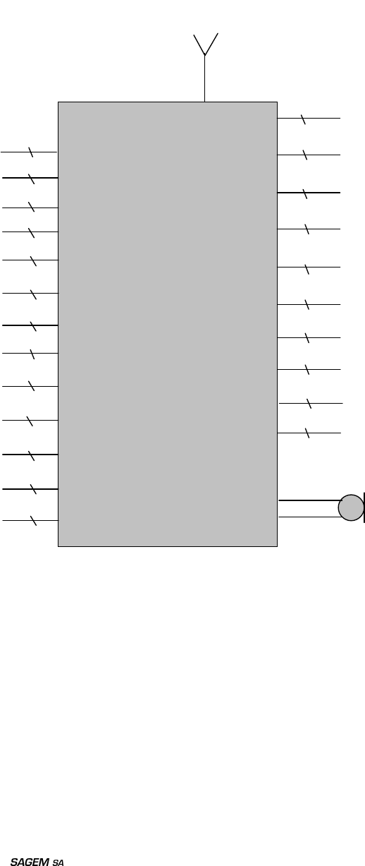
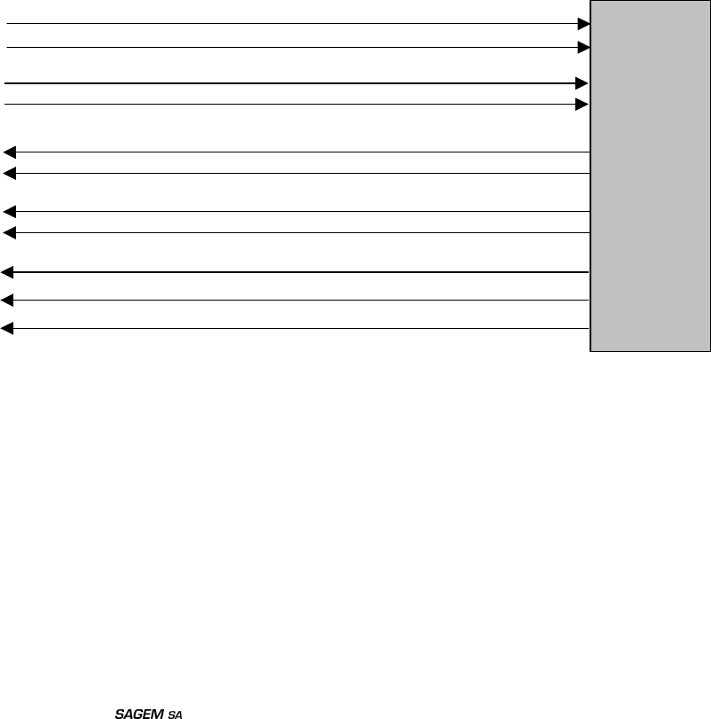
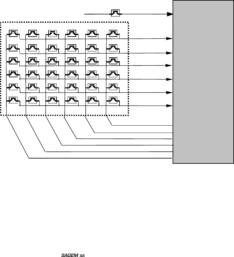
%/2&',$*5$0
)LJXUH
&2EORFGLDJUDP
See Ball-out chapter for more details.
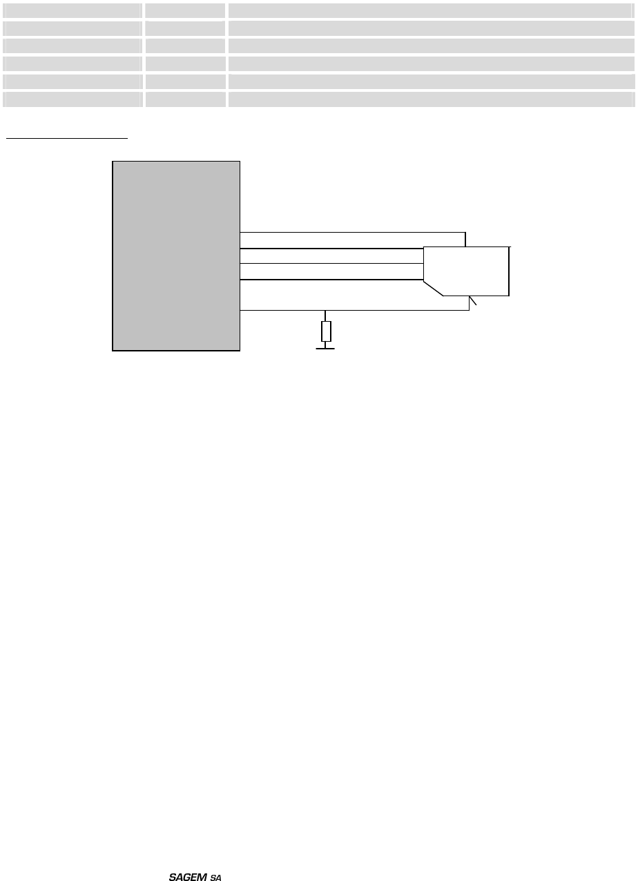
)81&7,21$/'(6&5,37,21
6,0
The SIM Card interface is compatible with the ISO 7816-3 IC card standard on the issues required by the
GSM 11.11 Phase 2+ standard. The module also supports Release 99 of the SIM Toolkit recommendation
and supports a Fixed Dialling Number directory.
The SIM Card interface insures the detection (SIMCD), the power on (SIMVCC) of the SIM Card and the
communication with it through a data signal (SIMIO), a clock signal (SIMCLK) and a reset signal (SIMRST).
Serial interface to LCD or
melody chip
Parallel interface (16bits)
to companion chip
Earphone 32 ohms
&2
PRGXOH
GPRS / GSM 850MHz
/ GSM900
/ DCS1800 / PCS1900
Keyboard
Battery charger
Battery (3.8V)
Vibrating device
MMC interface
SIM interface (3V)
Serial link 2 or IRDA
interface
V24
Antenna
Network LED
Microphone (accessory)
2
1
4
22
8
5
3
10
13
5
9
2
2
Stereo earphone
3
USB interface
3
Bluetooth interface
(MCSI) -optional
5
Spare I/Os
4
Interruption Inputs
2
Parallel interface
(8bits) to LCD
14
Sensor interface 14
Backup
1
I2S interface 5
Earphone 6 ohms min
2
Réf. : SCT TMO MASV3 SPEC 30
Rev. : H
Réf. sec. : 2x xxx xxx – x
Date : 12/05/04
DRAFT
Document . All rights of reproduction and disclosure reserved. Page 11
This document contains information on a product under development. SAGEM reserves the right to change or discontinue this product
without notice.
6LJQDO 3LQ1 'HVFULSWLRQ
SIMRST T8 SIM reset, provided by Base-band processor
SIMCLK T9 SIM clock, provided by Base-band processor
SIMIO T10 SIM serial data line, input and output
SIMVCC T7 SIM supply voltage
SIMCD B12 SIM insertion detection
SIM card connection:
)LJXUH
6,0FRQQHFWLRQ
The SIMCD signal should be connected to the SIM card reader in order to get SIMCD at low level (GND)
when no card is present and at high level (SIMVCC) when card is present (external pull down needed when
SIM card connector with detection is used).
This interface includes main protections.
&2
SIMVCC
SIMIO
SIMRST
SIMCLK
SIMCD
SIM card
In option
Réf. : SCT TMO MASV3 SPEC 30
Rev. : H
Réf. sec. : 2x xxx xxx – x
Date : 12/05/04
DRAFT
Document . All rights of reproduction and disclosure reserved. Page 12
This document contains information on a product under development. SAGEM reserves the right to change or discontinue this product
without notice.
$8',2
The module supports the following voice codecs:
• Half-Rate
• Full-Rate
• Enhanced Full Rate
It manages an external handset microphone (MICIP/MICIN) and an external handset earphone (32 ohms
HPP32/HPN32 and 6 ohms HPP8/HPN8) in differential mode.
The bias voltage of the microphone is provided directly on MICIP/MICIN pins (1.5V).
There are two options for the earphone:
- Two earphones, one 32 Ohms as earpiece and one 6 Ohms minimum as Ring/melody and as hands-
free loudspeaker if it is far from the microphone.
- one 32 Ohms earphone as earpiece.
The module can also manage accessories (earphone and microphone) through dedicated lines
(HSMICIP/HSMICIN for microphone and HSOL/HSGND/HSOR for stereo earphone). The typical impedance
for the earphone is 150ohms.
)LJXUH
$XGLR
This interface includes main protections.
To ensure proper operation of such sensitive signals, they have to be isolated from the other by ground on
mother board layout.
NB: To avoid destruction of module components, the HP inductance has to be 47nH +/- 5% @ 200MHz
Base-band
Ampli+Filter
MICIP
MICIN
HSMI
CIP
P
HSMICIN
HPP32
HPN32
HSGND
HSOR
HSOL
HPP8
HPN8
Réf. : SCT TMO MASV3 SPEC 30
Rev. : H
Réf. sec. : 2x xxx xxx – x
Date : 12/05/04
DRAFT
Document . All rights of reproduction and disclosure reserved. Page 13
This document contains information on a product under development. SAGEM reserves the right to change or discontinue this product
without notice.
',63/$<
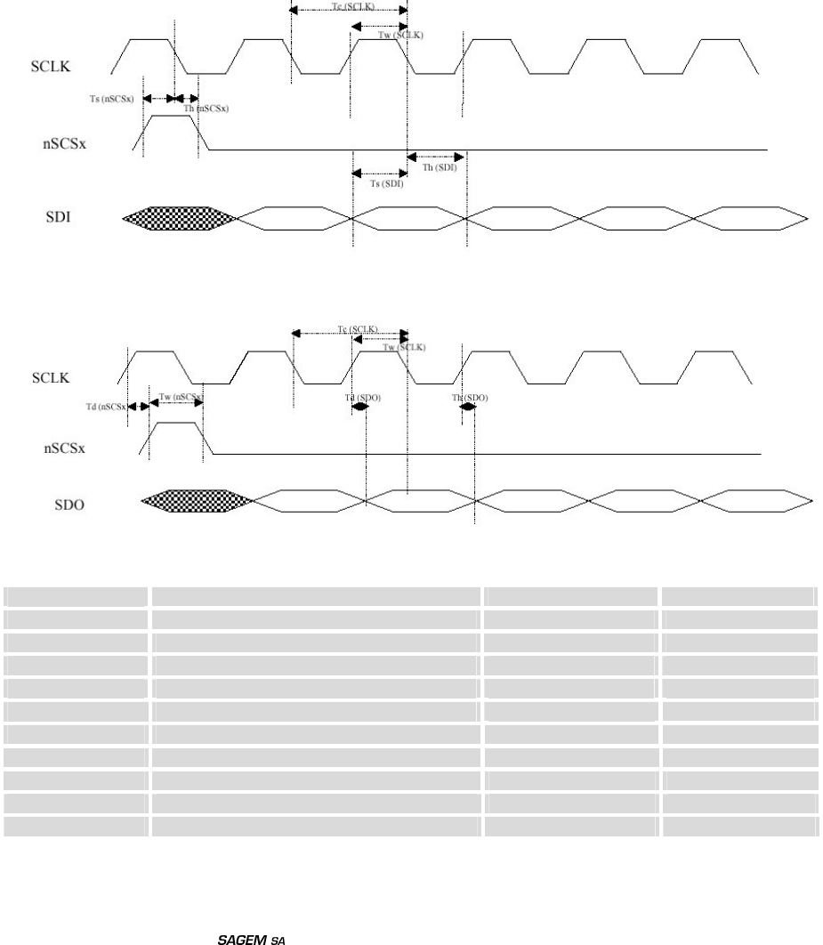
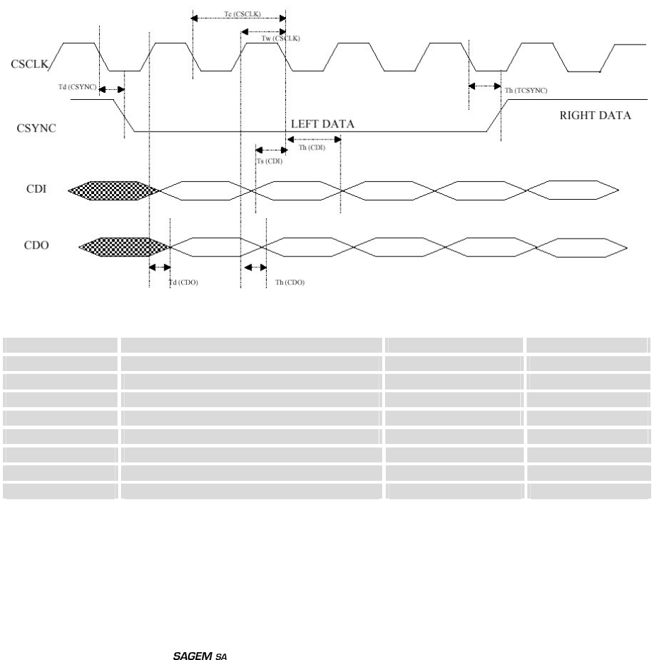
6HULDOLQWHUIDFH
A serial interface is provided on the module to manage an external LCD (256 colours) through data input
signal (DIMIW), data output signal (DOMIW), clock (CKMIW) and chip select (CSMIW1*).
Power supply of the LCD (VRIO) is also provided through this interface.
This interface could be used to manage one serial LCD or one melody chip (or other chipset using this
interface).
)LJXUH
6HULDOOLQNUHFHLYHWLPLQJ
)LJXUH
6HULDOOLQNWUDQVPLWWLPLQJ
7LPLQJ 'HVFULSWLRQ 0LQQV 0D[QV
Tw(SCLK) Pulse duration, serial port clock 38 -
Tc(SCLK) Cycle time, serial port clock 77 -
Td(SDO) Delay time, data valid after CLK falling - 10
Th(SDO) Hold time, data valid after CLK falling 0 -
Tw(nSCSx) Pulse duration, EN port 38 -
Td(nSCSx) Delay time, En after CLk rising 10 -
Ts(SDI) Setup, data valid before CLK rising 15 -
Th(SDI) Hold time, data valid after CLK rising 15 -
Ts(nSCSx) Setup, data valid before CLK falling 10 -
Th(nSCSx) Hold time, EN after CLK falling edge 10 -
This interface includes main protections.
Réf. : SCT TMO MASV3 SPEC 30
Rev. : H
Réf. sec. : 2x xxx xxx – x
Date : 12/05/04
DRAFT
Document . All rights of reproduction and disclosure reserved. Page 14
This document contains information on a product under development. SAGEM reserves the right to change or discontinue this product
without notice.
If specific LCD driver is used, the software would be provided by SAGEM, or at least the specific drivers will
be integrated by SAGEM. In that case a specific quotation is required.
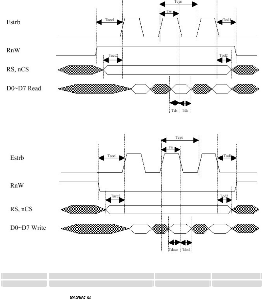
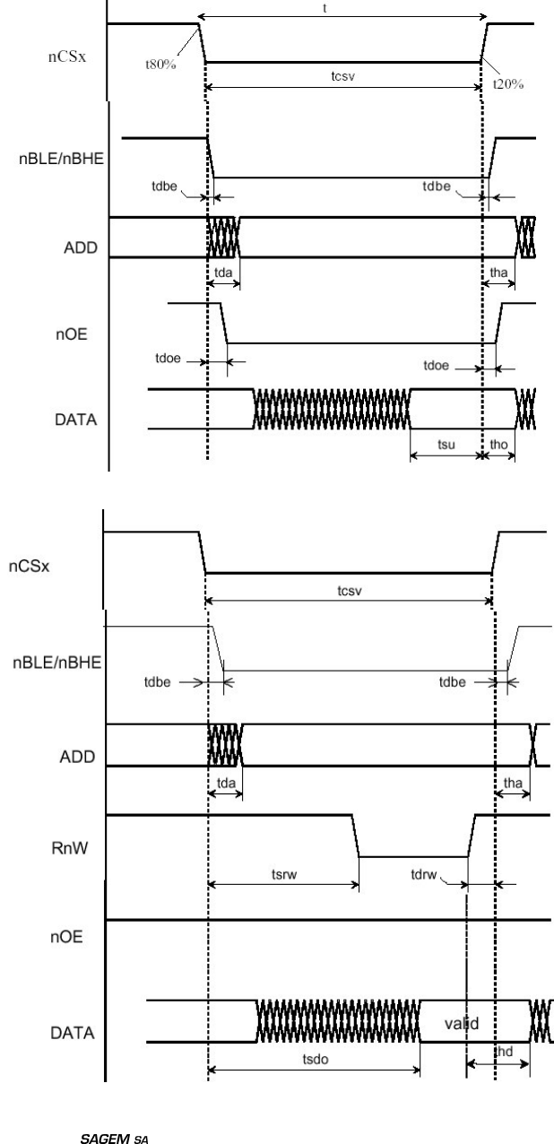
3DUDOOHOLQWHUIDFHWR/&'
A parallel interface is provided on the module to manage an external LCD (up to 262K colours) with data bus
(DLCD<0..7>), strobe enable (ESTRLCD), RWLCD*, RSLCD*, reset (RESETLCD*) and 2 chip select
(CS1LCD*, CS0LCD*).
NB: 65K and 262K colour LCDs have to be configured in 8 bits multi access mode.
)LJXUH
5HDGWLPLQJLQPRGH
)LJXUH
:ULWHWLPLQJLQPRGH
7LPLQJ 'HVFULSWLRQ 0LQQV 0D[QV
Tw(LCD) Pulse duration 38 -

Réf. : SCT TMO MASV3 SPEC 30
Rev. : H
Réf. sec. : 2x xxx xxx – x
Date : 12/05/04
DRAFT
Document . All rights of reproduction and disclosure reserved. Page 15
This document contains information on a product under development. SAGEM reserves the right to change or discontinue this product
without notice.
Tcyc Cycle time 77 -
Tacc1 Access time of RnW - 10
Tacc2 Access time off RS, nCS 0 -
Tod1 Output delay of RnW 38 -
Tod2 Output delay of RS, nCS 10 -
Tdacc Data access time 15 -
Tdod Data output disable time 15 -
Tds Setup time of read data 10 -
Tdh Hold time of read data 10 -
'$7$
'DWDVHUYLFHV
The module supports the following services:
• GPRS
• CSD: transparent and non-transparent up to 9600 BPS
• fax: class 1
Data sessions may be established over the main serial link, using the IrDA port (see below) or though the
USB interface.
,U'$
This UART interface is compatible with 16C750 compliant devices. It includes the slow infra-red protocol in
order to be connected with an infra-red transmitter to any external data peripherals with an IrDA compliant
data interface.
This IrDA interface (TXIR, RXIR and CMDIRDA) provided by the module is compliant with the IrDA 1.0 SIR
up to 115.2 Kbaud.
This interface could not be used at the same time as UART2 interface.
This interface includes main protections.
8$57
It is strongly recommended to leave this interface externally accessible for Debug.
This interface could not be used at the same time as IRDA interface.
9
A V24 interface is provided on external pins of the module with the following signals:
- RTS/CTS
- RX/TX
- DSR
- DTR
- DCD
- RI
It supports speeds up to 115.2 KBPS and may be used in auto bauding mode.
This interface includes main protections.
Réf. : SCT TMO MASV3 SPEC 30
Rev. : H
Réf. sec. : 2x xxx xxx – x
Date : 12/05/04
DRAFT
Document . All rights of reproduction and disclosure reserved. Page 16
This document contains information on a product under development. SAGEM reserves the right to change or discontinue this product
without notice.
86%
CO230 provides an USB 1.1, slave only, with the following signals: differential data (USB_DP, USB_DM)
and +5V input power supply (VCUSB).
$17(11$
The antenna connexion is prived through the ’antenna’ ball. This is a 50ohm RF connexion and as such must
be connected to the antenna via a proper 50ohm line; the RF ground is provided by the 5 balls surrounding
the antenna ball. A matching network might be required between the module antenna connexion and the
actual antenna to further adapt the antenna impedance to the module. An example of connexion is provided
in the application note together with some layout guidelines.
.(<3$'
A 6X6 keyboard could be managed by the module through the R1/R2/R3/R4/R5:R6 row signals and
C1/C2/C3/C4/C5:C6 column signals.
OUI signal performs the ON function. OFF signals performs OFF function.
Multi-key pressing is possible with this keyboard configuration.
)LJXUH
Keyboard connection
NC = these keys are connected internally in the CO230 module but are not managed.
The module uses the Tegic T9TM predictive input system.
9,'(26(1625
All the interfaces to connect a VGA video sensor are provided. Only power supply is not included.
R5
R4
R3
R2
C5
C4
C3
C2
C6
GREEN
GND
&2
R6
NC
NC
NC
#
9
NC
NC
NC
5
8
0
*
NC
NC
NC
P1
DO
LEFT
OK
LAT.
HIGH
RIGHT
UP
RED
P2
C1
4
7
6
MN
P3
R1
CL
NC
NC
3
2
1
LAT.
LOW
Réf. : SCT TMO MASV3 SPEC 30
Rev. : H
Réf. sec. : 2x xxx xxx – x
Date : 12/05/04
DRAFT
Document . All rights of reproduction and disclosure reserved. Page 17
This document contains information on a product under development. SAGEM reserves the right to change or discontinue this product
without notice.
,&LQWHUIDFH
A standard I2c interface is available on ball-out to send command to the video sensor.
3DUDOOHOLQWHUIDFHWRVHQVRU
A dedicated parallel interface is provided on ball-out with 8 bits data bus (DCAM<0..7>), vertical
synchronisation (VSCAM), horizontal synchronisation (HREF), input clock (PCLKCAM), configurable output
clock (XCLKCAM), reset (RESETCAM), standby (STBYCAM).
(;7(51$/&203$1,21&+,3,17(5)$&(
,6LQWHUIDFH
For audio transfer:
)LJXUH
,6WLPLQJ
7LPLQJ 'HVFULSWLRQ 0LQQV 0D[QV
Tw(CSCLK) Pulse duration 651 -
Tc(CSCLK) Cycle time 1302 -
Td(CDO) Delay time, data after CLK rising - 15
Th(CDO) Hold time, data valid after CLK rising 5 -
Ts(CDI) Setup, data valid before CLK falling 5 -
Th(CDI) Hold time, data valid after CLK falling 0 -
Td(CSYNC) Delay time, EN after CLK falling - 3
Th(CSYNC) Hold time, EN after CLK falling 2 -
3DUDOOHOLQWHUIDFHWRFRPSDQLRQFKLS
A parallel interface is provided on ball-out. This interface include 16 bits data lines (DPROC<0..15>), 3
address lines (APROC<1>, APROC<2>, APROC<3>), Write control signal RWPROC* (active low), Read
control signal OEPROC* (active low) and one chip select CS1PROC* (active low). This interface is dedicated
to external companion chip interface (as external DSP for additional multimedia applications).
This interface supports page mode.

Réf. : SCT TMO MASV3 SPEC 30
Rev. : H
Réf. sec. : 2x xxx xxx – x
Date : 12/05/04
DRAFT
Document . All rights of reproduction and disclosure reserved. Page 18
This document contains information on a product under development. SAGEM reserves the right to change or discontinue this product
without notice.
NB: The maximum capacitance acceptable on each signal of the parallel interface is 25pF (including copper
line capacitance, connectors capacitance…).
Réf. : SCT TMO MASV3 SPEC 30
Rev. : H
Réf. sec. : 2x xxx xxx – x
Date : 12/05/04
DRAFT
Document . All rights of reproduction and disclosure reserved. Page 19
This document contains information on a product under development. SAGEM reserves the right to change or discontinue this product
without notice.
)LJXUH
Parallel link read timing
)LJXUH
Parallel link write timing
Réf. : SCT TMO MASV3 SPEC 30
Rev. : H
Réf. sec. : 2x xxx xxx – x
Date : 12/05/04
DRAFT
Document . All rights of reproduction and disclosure reserved. Page 20
This document contains information on a product under development. SAGEM reserves the right to change or discontinue this product
without notice.
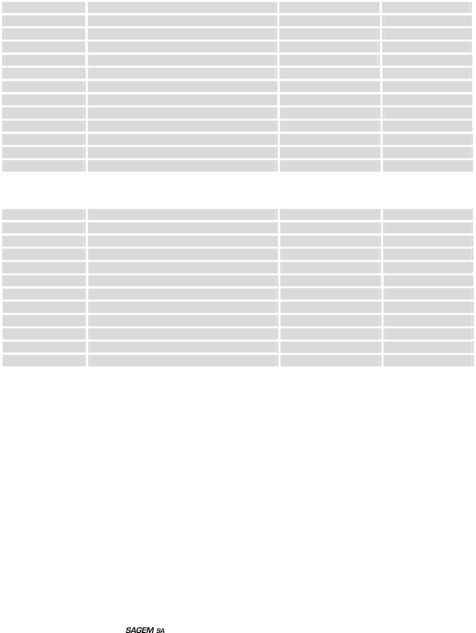
Single access:
7LPLQJ 'HVFULSWLRQ 0LQQV 0D[QV
tcyc CPU frequency - 1/Fcpu
tcsv Chip Select Valid tcyc (N+1)tcyc
tda NCS to Address valid - 1.2
tha Address hold from nCS 0 -
tdbe NBHE, nBLE to nCS - 0.6
tdoe NOE to nCS - 0.6
tsu Input data setup to nCS 5.5 -
tho Input data hold from nCS 0 -
tsrw NCS to RnW Tcyc/2-tdrw -
tdrw RnW to nCS 1.3 2.9
tdso NCS to output data valid - Tsrw+7.5
thd Output data hold from RnW 0 -
N= Wait State number
Page mode access:
7LPLQJ 'HVFULSWLRQ 0LQQV 0D[QV
tcyc CPU frequency - 1/Fcpu
tcsv Chip Select Valid tcyc (N+1)tcyc
tda NCS to Address valid - 1.5
tha Address hold from nCS 0 -
tdbe NBHE, nBLE to nCS - 0.8
tdoe NOE to nCS - 1.5
tsu1 Input data setup to nCS 5.2 -
tho1 Input data hold from nCS 0 -
tsu2 Input data setup to nCS 5.6 -
tho2 Address invalid time - 3
Tsa1sa2 Input data hold from nCS 0 -
Note: all timings computed for an external capacitance load of 10pF
NB: if needed, additional Wait State could be added by SAGEM.
%HFDUHIXOWKHPD[LPXPFDSDFLWDQFHFRPSRQHQWVOLQHVFRQQHFWRUV«
DFFHSWDEOHRQHDFKVLJQDORIWKHSDUDOOHOEXVLVS)
Réf. : SCT TMO MASV3 SPEC 30
Rev. : H
Réf. sec. : 2x xxx xxx – x
Date : 12/05/04
DRAFT
Document . All rights of reproduction and disclosure reserved. Page 21
This document contains information on a product under development. SAGEM reserves the right to change or discontinue this product
without notice.
%/8(7227+237,21$/
All the interfaces to connect a blue tooth chipset are provided. Only power supply is not included.
Blue tooth chipset management is optional.
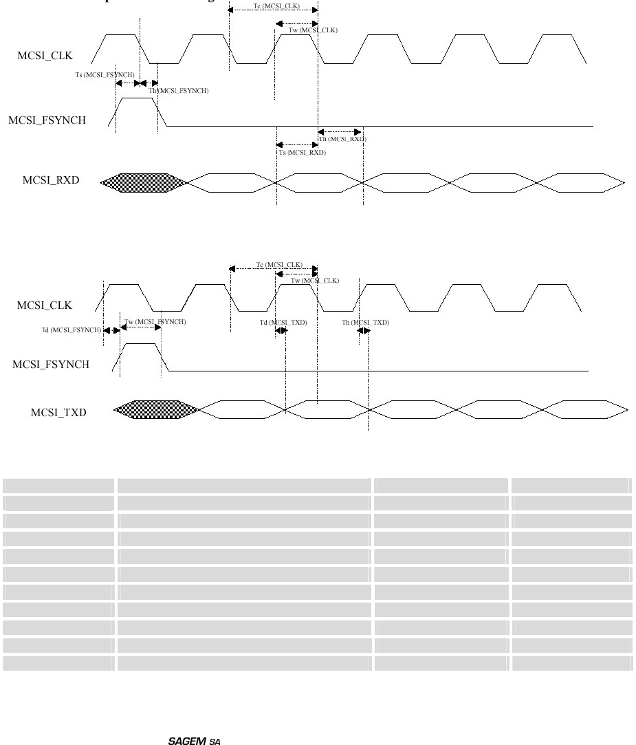
0&6,LQWHUIDFH
For audio transfer:
)LJXUH
%OXHWRRWKUHFHLYHWLPLQJ
)LJXUH
%OXHWRRWKWUDQVPLWWLPLQJ
7LPLQJ 'HVFULSWLRQ 0LQQV 0D[QV
Tw(MCSI_CLK) Pulse duration 77 -
Tc(MCSICLK) Cycle time 154 -
Td(MCSI_DO) Delay time, data after CLK rising - 10
Th(MCSI_DO) Hold time, data valid after CLK rising 0 -
Td(MCSI_FSYNCH) Delay time, EN after CLK falling - 10
Tw(MCSI_FSYNCH) Pulse duration, EN after CLK falling 77 -
Ts(MCSI_DI) Setup, data valid before CLK falling 15 -
Th(MCSI_DI) Hold time, data valid after CLK falling 15 -
Ts(MCSI_FSYNCH) Setup time, EN after CLK falling 10 -
Th(MCSI_FSYNCH) Hold time, EN after CLK falling 10 -

Réf. : SCT TMO MASV3 SPEC 30
Rev. : H
Réf. sec. : 2x xxx xxx – x
Date : 12/05/04
DRAFT
Document . All rights of reproduction and disclosure reserved. Page 22
This document contains information on a product under development. SAGEM reserves the right to change or discontinue this product
without notice.
8$57LQWHUIDFH
See UART interface from the V24 interface or from the IRDA interface.
&ORFN
26MHz clock could be used for clock input of blue tooth component (please note: 13MHz clock is also
available on CO230 ball-out but is not compliant with blue tooth chipsets features).
0(/2'<*(1(5$7,21
An external melody chip could be connected to the CO230 module through the following links:
- I2S for audio transfer
- Microwire for command
- 13MHz for melody chip clocking
Please note: if the melody chip is connected to the microwire, no serial LCD could be connected.
All these interfaces are described in the previous chapters.
'$,
A DAI interface is provided on the module for type approval tests.
&/2&.6
A 32KHz frequency clock, a 13MHz frequency digital clock and a 26MHz frequency analogic clock are
provided on external pins of the module.
The 13MHz clock could be used for the melody chip.
The 26MHz clock could be used for the blue tooth interface.
To ensure proper operation of such sensitive signals, they have to be isolated from the other by ground on
mother board layout.
32:(50$1$*(0(17$1'&+$5*(
%DWWHU\
The power supply signal VBAT is 3.45V to 4.5V range and 3.8V nominal.
Only Li-Ion battery are supported.
It has to be more than 3.2V, even during transients in order to avoid unwanted resets. The power supply
dropout has to be limited to 450mV, when the current consumption goes from minimum to maximum (0.1 to
2A). The noise level of the power supply has to be limited to 50mV RMS in the 100MHz – 1MHz frequency
range
SAGEM advises to use Sanyo or LG battery. If battery is used, SAGEM agreement is needed (slight
qualification tests).
Only battery with 200mohms maximum internal resistor are managed by the module.
External capacitor of 47uF has to be added as near as possible from the battery connector of mother board
for charge needs.
Réf. : SCT TMO MASV3 SPEC 30
Rev. : H
Réf. sec. : 2x xxx xxx – x
Date : 12/05/04
DRAFT
Document . All rights of reproduction and disclosure reserved. Page 23
This document contains information on a product under development. SAGEM reserves the right to change or discontinue this product
without notice.
95,2
+2.8V output is available on external pin of the module and could supply +2.8V external components (current
capability 10mA in active mode).
This interface includes main protections.
9EDFNXS
External Backup could be supply through the VBACKUP input (from 2.2V to 3.2V). A internal mechanism is
present to charge the backup battery.
If No external Backup is supplied, VBACKUP input has to be connected to VBAT signal.
&KDUJH
This interface manages the charge for regulated charger, when a charger is connected, even in
the following conditions: deeply discharged battery, short-circuited battery and unconnected battery (600mA
with regulated charger).
The interface manages the charge of some un regulated chargers, that have to be qualified by SAGEM (see
listing in application note).
This interface includes main protections.
$&&(6625,(6
Accessories connection has to be defined more precisely.
With the CO230 module, the following accessories could be connected :
- a pedestrian stereo or non stereo hand-free kit
- a battery charger
- an automotive hand-free kit
- a data cable
- an USB cable
These interfaces includes main protections.
)ODS
IO5 is dedicated for Flap detection.
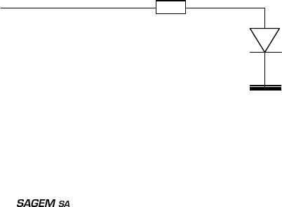
1HWZRUN/('
Commands for Green and Red LED are provided.
)LJXUH
/('GHYLFHFRQQHFWLRQ
LEDR or
LEDG
Réf. : SCT TMO MASV3 SPEC 30
Rev. : H
Réf. sec. : 2x xxx xxx – x
Date : 12/05/04
DRAFT
Document . All rights of reproduction and disclosure reserved. Page 24
This document contains information on a product under development. SAGEM reserves the right to change or discontinue this product
without notice.
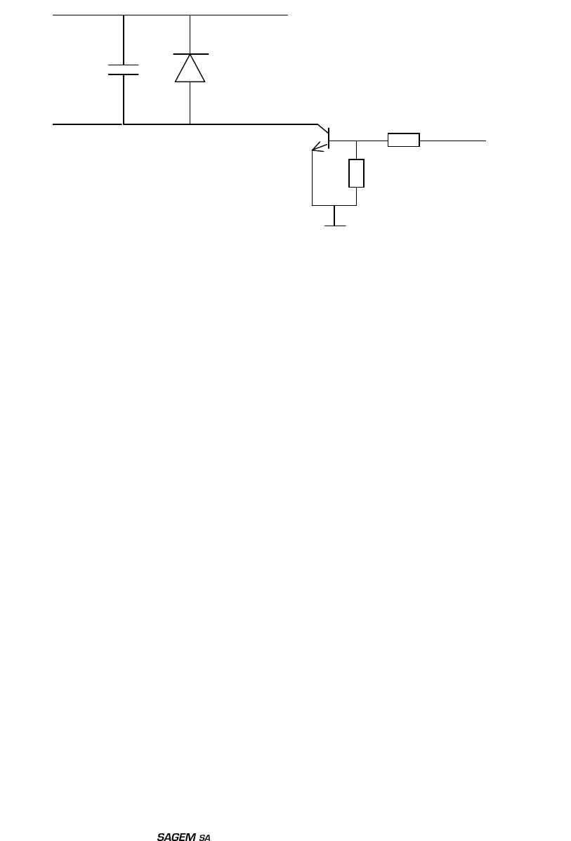
9LEUDWLQJGHYLFH
Vibrating device control is provided but external transistor is needed.
)LJXUH
9LEUDWLQJGHYLFHFRQQHFWLRQ
VIB+
VIB-
VBAT
CMDVIB
Réf. : SCT TMO MASV3 SPEC 30
Rev. : H
Réf. sec. : 2x xxx xxx – x
Date : 12/05/04
DRAFT
Document . All rights of reproduction and disclosure reserved. Page 25
This document contains information on a product under development. SAGEM reserves the right to change or discontinue this product
without notice.
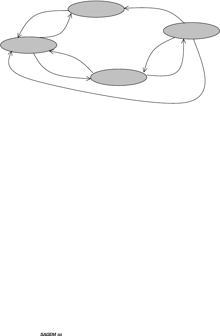
23(5$7,1*02'(6
)LJXUH
2SHUDWLQJPRGHVVWDWHGLDJUDP
02'(6'(6&5,37,21
1RVXSSO\
VBAT < 3.2V and VBACKUP < 2.2V.
All functions and power supplies are OFF: VRIO = 0.
2))
VBAT > 3.2V or external Backup VBACKUP > 2.2V.
The RTC only is running (32kHz). All other functions and power supplies are OFF: VRIO = 0.
$FWLYH
The module is active: all the functions are running and all the power supplies are ON and in full power mode
(full consumption).
VRIO = +2.8V
6WDQGE\
The module is in standby mode: the power supplies are ON and in low power mode.
This mode is typically use when the module is connected to the network and checking periodically if there is
an incoming call.
75$16,7,216'(6&5,37,21
3RZHUBRQ
A battery is connected to the module with VBAT > 3.2V (and/or VBACKUP is switched ON).
Wake-up
Sleep (automatic)
Switch_off
Switch_on
Switch_off
Power_on
Power_off
Power_off
No supply
OFF
Active
Standby

Réf. : SCT TMO MASV3 SPEC 30
Rev. : H
Réf. sec. : 2x xxx xxx – x
Date : 12/05/04
DRAFT
Document . All rights of reproduction and disclosure reserved. Page 26
This document contains information on a product under development. SAGEM reserves the right to change or discontinue this product
without notice.
3RZHUBRII
The battery is removed from the module (and/or VBACKUP is switched OFF).
6ZLWFKBRQ
The battery is already connected. The module starts when ON key is pressed or a charger is connected or
when wake up occurs.
6ZLWFKBRII
The battery is connected. The software is turning off of the module when OFF key is pressed and VBAT >
3.2V.
:DNHXS
The actions to go from standby mode to active mode are:
- Charger connection
- Key pressed
- Incoming call
- Data cable connection
- V24 activity
Réf. : SCT TMO MASV3 SPEC 30
Rev. : H
Réf. sec. : 2x xxx xxx – x
Date : 12/05/04
DRAFT
Document . All rights of reproduction and disclosure reserved. Page 27
This document contains information on a product under development. SAGEM reserves the right to change or discontinue this product without notice.
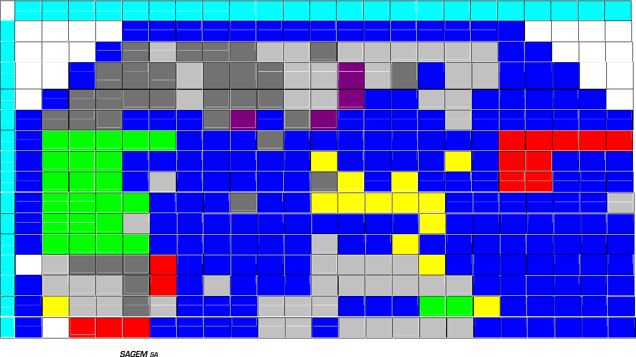
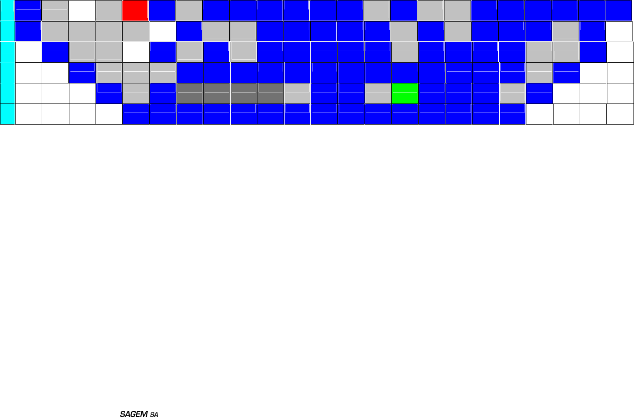
%$//287
The following list of signals could change.
$
GND GND GND GND GND GND GND GND GND GND GND GND GND GND GND
%
GND TXD1
TXIR RXD1
TXD2
RXD2
OUI* SDAI2
C SIMC
D POW
MMC CDMM
C DMMC
<1> DMMC
<2> DMMC
<3> EMU1*
GND GND
&
GND DCAM
<1> CTS DCAM
<4> CMDI
RDA DCAM
<2> DCAM
<6> PCLK
CAM SCLI2
C CMDM
MC MCSI
DI TDIDI
GIT XCLK
CAM GND TSPA
CTEX
T
EMU0*
GND GND GND
'
GND DTR RTS DCAM
<7> ALEN
AND RXIR
RBNA
ND* CLEN
AND DCAM
<0> CLKM
MC DMMC
<0> MCSI
DO GND GND BSCA
N* TDODI
GIT GND GND GND GND GND
(
GND DCD DSR RENA
ND GND GND GND CE1N
AND MCSIS
YNCH
GND DCAM
<3> MCSI
CLK GND GND GND GND IO11 GND GND GND GND GND GND
)
GND APRO
C<3>
APRO
C<2>
APRO
C<1>
OEPR
OC* CSPR
OC1*
GND GND GND DCAM
<5> GND GND GND GND GND GND GND GND VBAT
VBAT
VBAT
VBAT
VBAT
*
GND DPRO
C<15>
DPRO
C<14>
DPRO
C<13>
GND GND GND GND GND GND GND CS1L
CD* GND GND GND GND DLCD
<4> GND VBAT
VBAT
GND GND GND
+
GND DPRO
C<10>
DPRO
C<11>
DPRO
C<12>
GND INTI2C
GND GND GND GND GND WP1N
ANDL
CS0L
CD* GND DLCD
<6> GND GND GND VBAT
VBAT
GND GND GND
,
GND DPRO
C<9>
DPRO
C<8>
DPRO
C<7>
RWPR
OC* GND GND GND WENA
ND GND GND DLCD
<3> DLCD
<0> ESTR
BLCD
DLCD
<7> RSLC
D GND GND GND GND GND GND ANTE
NNE
-
GND DPRO
C<4>
DPRO
C<5>
DPRO
C<6>
IO7 GND GND GND GND GND GND GND GND GND GND RWLC
D* GND GND GND GND GND GND GND
.
GND DPRO
C<3>
DPRO
C<2>
DPRO
C<1>
DPRO
C<0>
GND GND GND GND GND GND CRES
ET GND GND DLCD
<5> GND GND GND GND GND GND GND GND
/
NC DAICL
K RESE
TCAM
HREF
CAM VSCA
M LEDC
GND GND GND GND GND CLK13
M C5 R5 C1 DLCD
<2> GND GND GND GND GND GND GND
0
GND DAIIN
DAIOU
T DAIRS
T STBY
CAM VCCS
GND CDO GND GND GND C3 C4 C6 R6 C2 CMDV
IB GND GND GND GND GND GND
1
GND RESE
TLCDL
IO6 IO5 RI ITDAT
A GND GND GND HPN8
HPP32
HSGN
D GND GND GND USB_
DP USB_
DM DLCD
<1> GND GND GND GND GND
2
GND NC CHAR
GEUR
CHAR
GEUR
CHAR
GEUR
GND GND GND GND HPP8
HPN3
2 GND HSOR
HSOL
HSMI
CIP CDI R1 GND GND GND GND GND GND
Réf. : SCT TMO MASV3 SPEC 30
Rev. : H
Réf. sec. : 2x xxx xxx – x
Date : 12/05/04
DRAFT
Document . All rights of reproduction and disclosure reserved. Page 28
This document contains information on a product under development. SAGEM reserves the right to change or discontinue this product without notice.
3
GND LEDR
NC TEST
RST VBAC
KUP GND TDOA
NALO
GND GND GND GND GND GND HSMI
CIN GND R3 R2 GND GND GND GND GND GND
4
GND LEDG
INT1 VRIO
ADC2
NC GND CSYN
C CSCL
K GND GND GND GND GND MICIN
GND R4 GND GND GND TSPC
LK GND
5
GND CSMI
W2* ENLE
D NC GND CLK32
K GND TDIAN
ALO GND GND GND GND GND MICIP
GND GND GND GND TSPDI
TSPE
NI* GND
6
GND DOMI
W CKMI
W CSMI
W1* GND GND GND GND GND GND GND GND GND GND GND GND GND TSPD
O GND
7
GND DIMIW
GND SIMVC
C SIMRS
T SIMCL
K SIMIO
TCK GND GND TMS VCUS
B GND GND GND CLK26
M GND
8
GND GND GND GND GND GND GND GND GND GND GND GND GND GND GND

Réf. : SCT TMO MASV3 SPEC 30
Rev. : H
Réf. sec. : 2x xxx xxx – x
Date : 12/05/04
DRAFT
Document . All rights of reproduction and disclosure reserved. Page 29
This document contains information on a product under development. SAGEM reserves the right to change or discontinue this product
without notice.
6LJQDOQDPH ,2W\SH )XQFWLRQ 'HVFULSWLRQ 3LQ1
DAIRST Input DAI reset M4
DAIOUT Output DAI output data M3
DAIIN Input DAI input data M2
DAICLK Input
DAI interface
DAI clock L2
DIMIW Input LCD driver input data of the serial link T5
DOMIW Output LCD driver output data of the serial link
S4
CKMIW Output LCD driver clock of the serial link S5
CSMIW1* Output
Serial interface to
connect LCD or chip
melody (1 chip select)
LCD driver chip select of the serial link S6
CSMIW2* Output Serial interface for
LED chipset Chip select for Baklight component R3
ENLED Output LED Chipset
command Enable for Backlight component R4
LEDR Output Red LED command P2
LEDG Output Green LED comment
Q2
R1 Input Keyboard row 1 O17
R2 Input Keyboard row 2 P17
R3 Input Keyboard row 3 P16
R4 Input Keyboard row 4 Q17
R5 Input Keyboard row 5 L14
R6 Input Keyboard row 6 M15
C6 Output Keyboard column 6 M14
C5 Output Keyboard column 5 L13
C4 Output Keyboard column 4 M13
C3 Output Keyboard column 3 M12
C2 Output Keyboard column 2 M16
C1 Output
Keyboard interface
Keyboard column 1 L15
OUI* Input ON key Keyboard ON key B10
SIMVCC Output SIM power supply T7
SIMRST Output SIM reset T8
SIMCLK Output SIM clock T9
SIMIO In/output SIM data T10
SIMCD Input
SIM interface
SIM insertion detection B12
HSMICIP Input Differential input from microphone O15
HSMICIN
Input
To external
microphone
(accessory) Differential input from microphone
P14
HSOL Output O14
HSGND Output N12
HSOR Output
To external stereo HP
(accessory)
O13
MICIP Input Differential input to handset microphone
R15
MICIN Input
Microphone interface
Differential input to handset microphone
Q15
HPP32 Output Differential output to 32ohms earphone
N11
HPN32 Output
Earphone interface
Differential output to 32ohms earphone
O11
HPP8 Output Differential output to 8ohms earphone O10
HPN8 Output Differential output to 8ohms earphone N10
CMDVIB Output Vibrating device
interface Vibrating device command M17
RI Output Ring Indicator N5
DSR Output
V24 interface with
flow control Data Send Ready E3

Réf. : SCT TMO MASV3 SPEC 30
Rev. : H
Réf. sec. : 2x xxx xxx – x
Date : 12/05/04
DRAFT
Document . All rights of reproduction and disclosure reserved. Page 30
This document contains information on a product under development. SAGEM reserves the right to change or discontinue this product
without notice.
DCD Output Data Carrier Detect E2
DTR Input Data Terminal Ready D3
CTS Output Clear To Send C5
RTS Input Request To Send D4
TXD1 Output UART transmit 1 B5
RXD1 Input
UART receive 1 B7
TXD2 Output UART transmit 2 B8
RXD2 Input
UART interface
UART receive 2 B9
TXIR Output IRDA transmit B6
RXIR Input IRDA receive D7
CMDIRDA Output
IRDA interface
IRDA command C7
INT1 Input Interrupt Q3
SCLI2C Output Clock C11
SDAI2C In/out Data B11
INTI2C Output
I2C interface
Interrupt H6
CHARGEUR Input Charge O3,O4,O5
VCCS Input M6
LEDC Output
Load interface
LED connection for charge activity L6
TESTRST Input Reset Reset system signal P4
ITDATA Input Accessories detection
Interrupt signal N6
DPROC<0> In/output Data bus K5
DPROC<1> In/output Data bus K4
DPROC<2> In/output Data bus K3
DPROC<3> In/output Data bus K2
DPROC<4> In/output Data bus J2
DPROC<5> In/output Data bus J3
DPROC<6> In/output Data bus J4
DPROC<7> In/output Data bus I4
DPROC<8> In/output Data bus I3
DPROC<9> In/output Data bus I2
DPROC<10> In/output Data bus H2
DPROC<11> In/output Data bus H3
DPROC<12> In/output Data bus H4
DPROC<13> In/output Data bus G4
DPROC<14> In/output Data bus G3
DPROC<15> In/output Data bus G2
RWPROC* Output Write I5
OEPROC* Output Read F5
CSPROC1* Output Chip select 1 F6
APROC<1> Output Address bus F4
APROC<2> Output Address bus F3
APROC<3> Output
Parallel interface
For
Companion chip
connection
Address bus F2
DLCD<0> In/output Data bus I13
DLCD<1> In/output Data bus N18
DLCD<2> In/output Data bus L16
DLCD<3> In/output Data bus I12
DLCD<4> In/output Data bus G17
DLCD<5> In/output
Parallel
LCD interface
Data bus K15

Réf. : SCT TMO MASV3 SPEC 30
Rev. : H
Réf. sec. : 2x xxx xxx – x
Date : 12/05/04
DRAFT
Document . All rights of reproduction and disclosure reserved. Page 31
This document contains information on a product under development. SAGEM reserves the right to change or discontinue this product
without notice.
DLCD<6> In/output Data bus H15
DLCD<7> In/output Data bus I15
ESTRBLCD Output Strobe enable I14
CS0LCD* Output Chip select 0 H13
CS1LCD* Output Chip select 1 G12
RSLCD* Output LCD register selection (data/control) I16
RWLCD* Output Read/write J16
RESETLCD* Output
Reset N2
USB_DP In/output N16
USB_DM In/output
Differential data
N17
VCUSB Input
USB interface
Power supply input T15
TSPACTEXT Output Radio signal C17
CSYNC In/output Synchronisation Q8
CSCLK In/output Clock Q9
CDI Input Data input O16
CDO Output Data output M8
CRESET Output
I2S
Reset K12
DCAM<0> In/output Data bus D10
DCAM<1> In/output Data bus C4
DCAM<2> In/output Data bus C8
DCAM<3> In/output Data bus E11
DCAM<4> In/output Data bus C6
DCAM<5> In/output Data bus F10
DCAM<6> In/output Data bus C9
DCAM<7> In/output Data bus D5
RESETCAM Output Reset L3
STBYCAM Output Standby M5
PCLKCAM Input Clock input C10
VSCAM Output Clock output L5
HREFCAM Output Horizontal synchronisation L4
XCLKCAM Output
Sensor interface
Vertical synchronisation C15
WP1NAND* Output H12
WENAND Output I9
RENAND Output E4
CLENAND Output D9
ALENAND Output D6
RBNAND* Input D8
CE1NAND Output
Specific interface
E8
DMMC<0> In/output Data bus D12
DMMC<1> In/output Data bus B15
DMMC<2> In/output Data bus B16
DMMC<3> In/output Data bus B17
CLKMMC Output Clock D11
CMDMMC In/output Control C12
POWMMC Output Power supply control B13
CDMMC Input
MMC interface
Card detect B14
CLK26M Output 26MHz analog clock output T19
CLK13M Output
Clocks
13MHz digital clock output L12
Réf. : SCT TMO MASV3 SPEC 30
Rev. : H
Réf. sec. : 2x xxx xxx – x
Date : 12/05/04
DRAFT
Document . All rights of reproduction and disclosure reserved. Page 32
This document contains information on a product under development. SAGEM reserves the right to change or discontinue this product
without notice.
CLK32K Output 32KHz digital clock output R7
ADC2 Input ADC Battery type detection Q5
MCSIDI Input Data input C13
MCSIDO Output Data output D13
MCSICLK In/output Clock SPI E12
MCSISYNCH In/output Synchronisation E9
IO5 In/output With Pull down N4
IO6 In/output With pull down N3
IO7 In/output With pull down J5
IO11 In/output
MCSI interface
With pull up E17
VBAT Input +3.6V battery power supply F19,F20,F21,
F22,F23,G19,
G20,H19,H20
VRIO Output +2.8V output power supply Q4
VBACKUP Input
Power supply
Backup input P5
GND Ground Ground GND Other
ANTENNE Output/input Antenna input/output Antenna connection (50 ohms) I23
TCK Input JTAG T11
TMS Input JTAG T14
TDIDIGIT Input JTAG C14
TDODIGIT Output JTAG D17
TDIANALOG Input JTAG R9
TDOANALOG Output
JTAG interface
JTAG P7
BSCAN* Input Boundary scan JTAG D16
EMU0* Output For debug C18
EMU1* Output For debug B18
NC NC No connect Q21,R21,R20
,S20, L1, P3,
Q6, R5, O2
Réf. : SCT TMO MASV3 SPEC 30
Rev. : H
Réf. sec. : 2x xxx xxx – x
Date : 12/05/04
DRAFT
Document . All rights of reproduction and disclosure reserved. Page 33
This document contains information on a product under development. SAGEM reserves the right to change or discontinue this product without
notice.
(/(&75,&$/63(&,),&$7,21
VOH High level output voltage
VOL Low level output voltage
VIH High level input voltage
VIL Low level input voltage
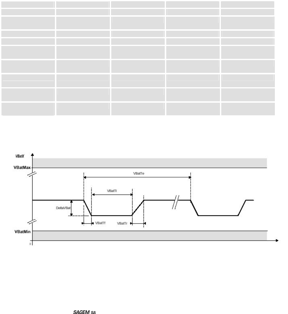
9%$7
The module is supplied through the VBAT signal with the following characteristics:
3DUDPHWHU 1DPH 0LQ 7\S 0D[
VBAT period (ms) VbatTe (*) 4.614 4.615 DC
VBAT low duration
(us) VbatTi (*) 550 - VBAT period
VBAT rise time (us) VbatTr (*) 0 - -
VBAT fall time (us) VbatTf (*) 0 - -
VBAT maximum
voltage (V) VbatMax (*) - - 4.5
VBAT minimum
voltage (V) VbatMin (*) 3.45 - -
VBAT drop voltage
(mV) DeltaVbat (*) - - 450 (**)
Transient voltage
(V) 3 - -
Noise level (Vrms)
@100MHz-1MHz - - 50mV
(*): cf figure 16.
(**): for a new battery. Of course for an old battery, this value will be higher and will create a reset (without MMI
message) when the battery begins to be discharged.
)LJXUH
9%$7YROWDJHZDYHIRUP
Réf. : SCT TMO MASV3 SPEC 30
Rev. : H
Réf. sec. : 2x xxx xxx – x
Date : 12/05/04
DRAFT
Document . All rights of reproduction and disclosure reserved. Page 34
This document contains information on a product under development. SAGEM reserves the right to change or discontinue this product without
notice.
95,2
6LJQDO 0LQ 7\S 0D[ 5HPDUNV
Voltage level (activ
mode) 2.70V 2.80V 2.90V
Voltage level (sleep
mode) 2.70V 2.80V 3.00V
Current capability
Active mode - - 10mA
Current capability
Sleep mode - - 0.5mA
Rise time - 10µs -
'$,,17(5)$&(
DAIRST, DAIIN, DAICLK and DAIOUT have the following characteristics:
9 9 9 9
6LJQDO
0LQ 0D[ 0LQ 0D[
5HPDUNV
DAIRST -0.5 +0.8 +2.03 +3.2
DAICLK -0.5 +0.8 +2.03 +3.2 PD 100K
DAIIN -0.5 +0.8 +2.03 +3.2 PD 100K
DAIOUT - +0.59 +2.32 -
1(7:25./('
9 9 9 9
6LJQDO
0LQ 0D[ 0LQ 0D[
5HPDUNV
LEDR, LEDG - +0.59 +2.32 -
LEDG: Imax = 2mA
LEDR: Imax = 4mA
6(5,$/,17(5)$&()25/&'
DIMIW, DOMIW, CKMIW, CSMIW1* have the following characteristics:
9 9 9 9
6LJQDO
0LQ 0D[ 0LQ 0D[
5HPDUNV
DIMIW -0.5 +0.8 +2.03 +3.2 PU 100K
DOMIW - +0.59 +2.32 -
CKMIW - +0.59 +2.32 -
CSMIW1* - +0.59 +2.32 -
.(<%2$5',17(5)$&(
R1, R2, R3, R4, R5, R6, C1, C2, C3, C4, C5 and C6 have the following characteristics:
9 9 9 9
6LJQDO
0LQ 0D[ 0LQ 0D[
5HPDUNV
Input (R1/2/3/4/5/6) -0.5 +0.8 +2.03 +3.2 ESD protection
PU
Output
(C1/2/3/4/5/6) - +0.59 +2.32 - ESD protection
OUI*:
Réf. : SCT TMO MASV3 SPEC 30
Rev. : H
Réf. sec. : 2x xxx xxx – x
Date : 12/05/04
DRAFT
Document . All rights of reproduction and disclosure reserved. Page 35
This document contains information on a product under development. SAGEM reserves the right to change or discontinue this product without
notice.
6LJQDO 0LQ 7\S 0D[ 5HPDUNV
Ton (ms) - 32,31 -
VIL - - 0.3*VBAT
VIH 0.7*VBAT - -
PU
9,%5$7,1*'(9,&(&21752/
CMDVIB have the following characteristics:
9 9 9 9
6LJQDO
0LQ 0D[ 0LQ 0D[
5HPDUNV
CMDVIB - +0.59 +2.32 - PD
ICMDVIB max = 2mA
9
RXD1, TXD1, CTS, RTS, DCD, DSR, DTR and RI have the following characteristics:
9 9 9 9
6LJQDO
0LQ 0D[ 0LQ 0D[
5HPDUNV
RTS -0.5 +0.8 +2.03 +3.2 PU 100K
RI - +0.59 +2.32 -
CTS - +0.59 +2.32 -
DSR - +0.59 +2.32 - PD
DCD - +0.59 +2.32 - PU 10K
DTR -0.5 +0.8 +2.03 +3.2 PU 100K
TXD1 - +0.59 +2.32 -
RXD1 -0.5 +0.8 +2.03 +3.2 PU 10K
,5'$$1'8$57
RXIR, TXIR and CMDIRDA have the following characteristics:
9 9 9 9
6LJQDO
0LQ 0D[ 0LQ 0D[
5HPDUNV
RXIR, RXD2 -0.5 +0.8 +2.03 +3.2 PU 100K
TXIR, TXD2,
CMDIRDA - +0.59 +2.32 -
5(6(7
TESTRST has the following characteristics:
6LJQDO 0LQ 0D[ 5HPDUNV
VL (V) - 0.2 VBAT
VH (V) 0.8 VBAT -
Treset (ms) 65 -
PD 100K
NB: The reset signal resets all the system including backup.
63$5(,2
IO5, 6,7,11 have the following characteristics:
6LJQDO 9 9 9 9 5HPDUNV
Réf. : SCT TMO MASV3 SPEC 30
Rev. : H
Réf. sec. : 2x xxx xxx – x
Date : 12/05/04
DRAFT
Document . All rights of reproduction and disclosure reserved. Page 36
This document contains information on a product under development. SAGEM reserves the right to change or discontinue this product without
notice.
0LQ 0D[ 0LQ 0D[
Input -0.5 +0.8 +2.03 +3.2
Output - +0.59 +2.32 -
IO5,6,7:
programmable PD
IO11:
programmable PU
Iout max = 2mA
&/2&.6
CLK26M and CLK32K have the following characteristics:
9 9 9 9
6LJQDO
0LQ 0D[ 0LQ 0D[
5HPDUNV
CLK13M - +0.59 +2.32 -
CLK32K - 0,297 1,32 -
6LJQDO 9 9 9 9 5HPDUNV
CLK26M 0.5V 2V
3$5$//(/,17(5)$&()25&203$1,21&+,3
DPROC<0..15>, APROC<1..3>, RWPROC*, OEPROC*, CS1PROC* have the following characteristics:
9 9 9 9
6LJQDO
0LQ 0D[ 0LQ 0D[
5HPDUNV
Input
DPROC<0..15> -0.5 +0.8 +2.03 +3.2
Output
DPROC<0..15>,
APROC<1..3>,
RWPROC*,
CS1PROC*,
OEPROC*
- +0.59 +2.32 -
NB: The maximum capacitance acceptable on each signal of the parallel interface for companion chip is 25pF
(including copper line capacitance, connectors capacitance…).
3$5$//(/,17(5)$&()25/&'
DLCD<0..7>, ESTRBLCD, RWLCD*, CS0LCD*, CS1LCD*, RESETLCD*, RSLCD have the following
characteristics:
9 9 9 9
6LJQDO
0LQ 0D[ 0LQ 0D[
5HPDUNV
Input
DLCD<0..7> -0.5 +0.8 +2.03 +3.2
Output
DLCD<0..15>,
RESETLCD*,
RWLCD*,
CS0LCD*,
CS1LCD*, RSLCD,
ESTRBLCD
- +0.59 +2.32 -
NB: The maximum capacitance acceptable on each signal of the parallel interface for LCD is tbd (including
copper line capacitance, connectors capacitance…).
Réf. : SCT TMO MASV3 SPEC 30
Rev. : H
Réf. sec. : 2x xxx xxx – x
Date : 12/05/04
DRAFT
Document . All rights of reproduction and disclosure reserved. Page 37
This document contains information on a product under development. SAGEM reserves the right to change or discontinue this product without
notice.
86%,17(5)$&(
USB_DM, USB_DP, VCUSB have the following characteristics:
9 9 9 9
6LJQDO
0LQ 0D[ 0LQ 0D[
5HPDUNV
Input
USB_DM, USB_DP -0.5 +0.93 +2.45 +3.6 PU
Output
USB_DM, USB_DP - +0.682 +2.8 - PU
6LJQDO 0LQ 0D[
VCUSB (V) 4.0 5.5
00&,17(5)$&(
DMMC<0..3>, CLKMMC, CMDMMC, POWMMC, CDMMC have the following characteristics:
9 9 9 9
6LJQDO
0LQ 0D[ 0LQ 0D[
5HPDUNV
Input
DMMC<0..3>,
CMDMMC
-0.5 +0.8 +2.03 +3.2 PU 100K
Output
DMMC<0..3>,
POWMMC,
CMDMMC
- +0.59 +2.32 - PU 100K
CLKMMC - +0.59 +2.32 -
9,'(26(1625,17(5)$&(
DCAM<0..7>, RESETCAM, STBYCAM, PCLKCAM, VSCAM, HREFCAM, XCLKCAM have the following
characteristics:
9 9 9 9
6LJQDO
0LQ 0D[ 0LQ 0D[
5HPDUNV
Input
DCAM<0..7>,
PCLKCAM
-0.5 +0.8 +2.03 +3.2
Output
DCAM<0..15>,
XCLKCAM,
HREFCAM
- +0.59 +2.32 -
VSCAM,
STBYCAM,
RESETCAM
- +0.59 +2.32 - Programmable PU
NB: The maximum capacitance acceptable on each signal of the parallel interface for video sensor is tbd
(including copper line capacitance, connectors capacitance…).
0&6,,17(5)$&(
MCSIDI, MCSIDO, MCSICLK, MCSISYNCH have the following characteristics:
9 9 9 9
6LJQDO
0LQ 0D[ 0LQ 0D[
5HPDUNV
Input
MCSIDI, MCSICLK,
MCSISYNCH
-0.5 +0.8 +2.03 +3.2
Réf. : SCT TMO MASV3 SPEC 30
Rev. : H
Réf. sec. : 2x xxx xxx – x
Date : 12/05/04
DRAFT
Document . All rights of reproduction and disclosure reserved. Page 38
This document contains information on a product under development. SAGEM reserves the right to change or discontinue this product without
notice.
Output
MCSIDO,
MCSICLK,
MCSISYNCH
- +0.59 +2.32 -
NB: a pull down as to be added to MCSIDI and MCSICLK
,6,17(5)$&(
CSYNC, CSCLK, CDI, CDO, CRESET have the following characteristics:
9 9 9 9
6LJQDO
0LQ 0D[ 0LQ 0D[
5HPDUNV
CDI -0.5 +0.8 +2.03 +3.2 PD 100K
Input
CSYNC, CSCLK -0.5 +0.8 +2.03 +3.2
Output
CDO, CRESET,
CSYNC, CSCLK
- +0.59 +2.32 -
,&,17(5)$&(
SDAI2C, SCLI2C, INTI2C have the following characteristics:
9 9 9 9
6LJQDO
0LQ 0D[ 0LQ 0D[
5HPDUNV
Input
SDAI2C, INTI2C -0.5 +0.8 +2.03 +3.2 Programmable PU
on INTI2C
Output
SDAI2C, SCLI2C - +0.59 +2.32 - PU 1.8K
-7$*,17(5)$&(
TCLK, TMS, TDI, TDODIGIT, TDIANALOG, BSCAN*, EMU0*, EMU1* have the following characteristics:
9 9 9 9
6LJQDO
0LQ 0D[ 0LQ 0D[
5HPDUNV
TMS, TDI,
TDIANALOG,
BSCAN*
-0.5 +0.8 +2.03 +3.2 PU
TCK -0.5 +0.8 +2.03 +3.2 PD
TDODIGIT,
TDOANALOG, - +0.59 +2.32 -
EMU0*, EMU1* - +0.59 +2.32 - PU
$'&
3DUDPHWHU 0LQ 7\S 0D[
Resolution - 10 bits -
Input range 0 - 1.75V
Input capacitor - 12pF -
,17(558376
ITDATA and INT1 have the following characteristics :
9 9 9 9
6LJQDO
0LQ 0D[ 0LQ 0D[
5HPDUNV

Réf. : SCT TMO MASV3 SPEC 30
Rev. : H
Réf. sec. : 2x xxx xxx – x
Date : 12/05/04
DRAFT
Document . All rights of reproduction and disclosure reserved. Page 39
This document contains information on a product under development. SAGEM reserves the right to change or discontinue this product without
notice.
ITDATA -0.5 +0.8 +2.03 +3.2 PU
INT1 -0.5 +0.8 +2.03 +3.2 PU
Pulse duration in functional mode: 77ns min.
9%$&.83
6LJQDO 0LQ 0D[ 5HPDUNV
VBACKUP +2.2V +3.2V
If no external backup is supplied, VBACKUP has to be connected to VBAT.
With external BACKUP:
- if VBAT < VBACKUP, internal RTC is supplied by VBACKUP.
- if VBAT > VBACKUP, internal RTC is supplied by VBAT.
Without external VBACKUP (VBACKUP input connected to VBAT)
- if VBAT > 2.2V, internal RTC is supplied by VBAT.
- if VBAT < 2.2V, internal RTC is not supplied.
(19,5210(17$/63(&,),&$7,21
23(5$7,1*&21',7,216
3DUDPHWHU 0LQ 0D[
Ambient temperature -10°C +55°C
Supply voltage VBAT +3.45V +4.5V
&/,0$7,&&21',7,216
3DUDPHWHU 0LQ 0D[
Ambient temperature
Normal range -10°C +55°C
Ambient temperature
Extended range -20°C +70°C
Storage temperature -40°C +85°C
Long damp heat
Operating conditions Tested at +60°C, 95% RH during 504 hours
Short damp heat
Storage and
transportation conditions
Tested at +40°C, 95% RH during 96 hours
Réf. : SCT TMO MASV3 SPEC 30
Rev. : H
Réf. sec. : 2x xxx xxx – x
Date : 12/05/04
DRAFT
Document . All rights of reproduction and disclosure reserved. Page 40
This document contains information on a product under development. SAGEM reserves the right to change or discontinue this product without
notice.
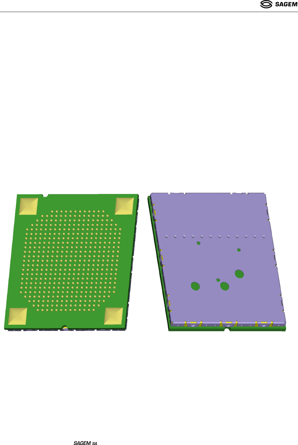
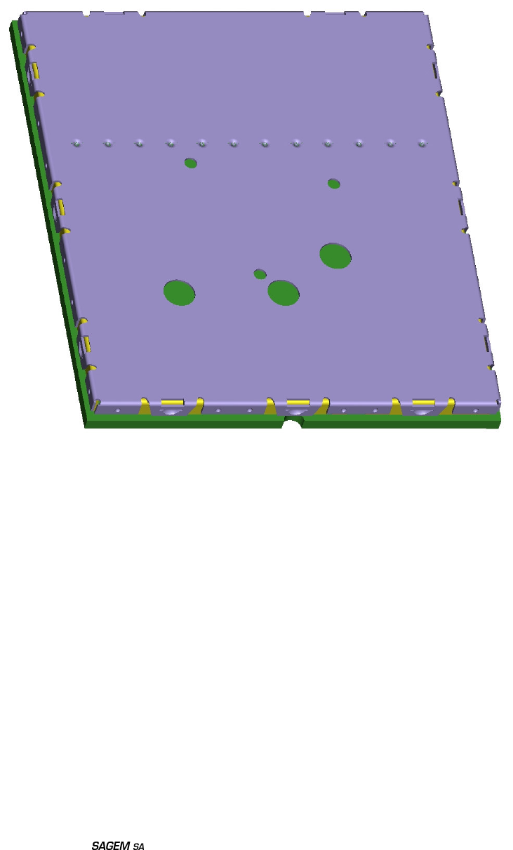
0(&+$1,&$/63(&,),&$7,21
)LJXUH
&2FRPSRQHQWVLGH
Réf. : SCT TMO MASV3 SPEC 30
Rev. : H
Réf. sec. : 2x xxx xxx – x
Date : 12/05/04
DRAFT
Document . All rights of reproduction and disclosure reserved. Page 41
This document contains information on a product under development. SAGEM reserves the right to change or discontinue this product without
notice.
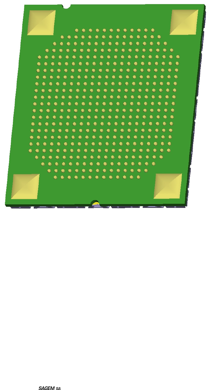
)LJXUH
&2EDOORXWVLGH
Réf. : SCT TMO MASV3 SPEC 30
Rev. : H
Réf. sec. : 2x xxx xxx – x
Date : 12/05/04
DRAFT
Document . All rights of reproduction and disclosure reserved. Page 42
This document contains information on a product under development. SAGEM reserves the right to change or discontinue this product without
notice.
)LJXUH
&2GLPHQVLRQV

Réf. : SCT TMO MASV3 SPEC 30
Rev. : H
Réf. sec. : 2x xxx xxx – x
Date : 12/05/04
DRAFT
Document . All rights of reproduction and disclosure reserved. Page 43
This document contains information on a product under development. SAGEM reserves the right to change or discontinue this product without
notice.
$11(;(
6LJQDOQDPH ,2W\SH 3LQ1
DAIRST Digital bi directional buffer (IDI041/OUK431) M4
DAIOUT Digital bi directional buffer (IDI041/OUK431) M3
DAIIN Digital bi directional buffer (IDI041/OUK431). Pull down M2
DAICLK Digital bi directional buffer (IDI041/OUI431). Pull down L2
DIMIW Digital input buffer (IDI041/PS0201). Pull up T5
DOMIW Digital output buffer (OUK431) S4
CKMIW Digital output buffer (OUI431) S5
CSMIW1* Digital output buffer (OUK431) S6
CSMIW2* Digital output buffer (OUK431) R3
ENLED Digital bi directional buffer (IDG091/OUI431/PE1001) R4
LEDR Digital output buffer (OUI831) P2
LEDG Digital output buffer (OUK431) Q2
R1 Digital bi directional buffer (IDI041/OUI431/PS1001). Pull up O17
R2 Digital bi directional buffer (IDI041/OUI431/PS1001). Pull up P17
R3 Digital bi directional buffer (IDI041/OUI431/PS1001). Pull up P16
R4 Digital bi directional buffer (IDI041/OUI431/PS1001). Pull up Q17
R5 Digital bi directional buffer (IDI041/OUI431/PS1001). Pull up L14
R6 Digital bi directional buffer (IDI041/OUI431/PS1001). Pull up M15
C6 Digital output buffer (OUO431) M14
C5 Digital output buffer (OUI431) L13
C4 Digital output buffer (OUI431) M13
C3 Digital output buffer (OUI431) M12
C2 Digital output buffer (OUI431) M16
C1 Digital output buffer (OUI431) L15
OUI* Digital input. Pull up B10
SIMVCC Power supply output T7
SIMRST Digital output buffer T8
SIMCLK Digital output buffer T9
SIMIO Digital bi directional buffer. Pull up T10
SIMCD Digital input buffer (IDI091). Pull down B12
HSMICIP Analog audio input O15
HSMICIN Analog audio input P14
HSOL Analog audio output O14
HSGND Analog audio output N12
HSOR Analog audio output O13
MICIP Analog audio input R15
MICIN Analog audio input Q15
HPP32 Analog audio output N11
HPN32 Analog audio output O11
HPP8 Analog audio output O10
HPN8 Analog audio output N10
CMDVIB Digital bi directional buffer (IDG091/OUI431/PE1001). Pull down M17
RI Digital bi directional buffer (IDG091/OUO431/PS1001) N5
DSR Digital bi directional buffer (IDG091/OUI431/PE1001). Pull down E3
DCD Digital output buffer (OUI831). Pull up E2

Réf. : SCT TMO MASV3 SPEC 30
Rev. : H
Réf. sec. : 2x xxx xxx – x
Date : 12/05/04
DRAFT
Document . All rights of reproduction and disclosure reserved. Page 44
This document contains information on a product under development. SAGEM reserves the right to change or discontinue this product without
notice.
DTR Digital bi directional buffer (IDI091/OUI831). Pull up D3
CTS Digital output buffer (OUI831). Pull up C5
RTS Digital bi directional buffer (IDI091/OUO431) D4
TXD1 Digital output buffer (OUI831) B5
RXD1 Digital bi directional buffer (IDI091/OUI831). Pull up B7
TXD2 Digital output buffer (OUI831) B8
RXD2 Digital input buffer (IDI091). Pull up B9
TXIR Digital bi directional buffer (IDI041/OUI831) B6
RXIR Digital bi directional buffer (IDI091/OUK431). Pull up D7
CMDIRDA Digital output buffer (OUK431) C7
INT1 Digital bi directional buffer (IDG091/OUI431/PS1001). Pull up Q3
SCLI2C Digital bi directional buffer (IDI091/UOS205). Pull up C11
SDAI2C Digital bi directional buffer (IDI091/UOS205). Pull up B11
INTI2C Digital bi directional buffer (IDG091/OUI431/PS1001). Pull up H6
CHARGEUR Power supply input O3,O4,O5
LEDC Analog output L6
TESTRST Digital input. Pull down P4
ITDATA Digital bi directional buffer (IDI091/OUI431/PS1001). Pull up N6
DPROC<0> Digital bi directional buffer (IDI041/OUI831) K5
DPROC<1> Digital bi directional buffer (IDI041/OUI831) K4
DPROC<2> Digital bi directional buffer (IDI041/OUI831) K3
DPROC<3> Digital bi directional buffer (IDI041/OUI831) K2
DPROC<4> Digital bi directional buffer (IDI041/OUI831) J2
DPROC<5> Digital bi directional buffer (IDI041/OUI831) J3
DPROC<6> Digital bi directional buffer (IDI041/OUI831) J4
DPROC<7> Digital bi directional buffer (IDI041/OUI831) I4
DPROC<8> Digital bi directional buffer (IDI041/OUI831) I3
DPROC<9> Digital bi directional buffer (IDI041/OUI831) I2
DPROC<10> Digital bi directional buffer (IDI041/OUI831) H2
DPROC<11> Digital bi directional buffer (IDI041/OUI831) H3
DPROC<12> Digital bi directional buffer (IDI041/OUI831) H4
DPROC<13> Digital bi directional buffer (IDI041/OUI831) G4
DPROC<14> Digital bi directional buffer (IDI041/OUI831) G3
DPROC<15> Digital bi directional buffer (IDI041/OUI831) G2
RWPROC* Digital bi directional buffer (IDI041/OUI831) I5
OEPROC* Digital output buffer (OUI831) F5
CSPROC1* Digital bi directional buffer (IDI041/OUI831) F6
APROC<1> Digital bi directional buffer (IDI041/OUI831) F4
APROC<2> Digital bi directional buffer (IDI041/OUI831) F3
APROC<3> Digital bi directional buffer (IDI041/OUI831) F2
DLCD<0> Digital bi directional buffer (IDI041/OUI431) I13
DLCD<1> Digital bi directional buffer (IDI041/OUI431) N18
DLCD<2> Digital bi directional buffer (IDI041/OUI431) L16
DLCD<3> Digital bi directional buffer (IDI041/OUI431) I12
DLCD<4> Digital bi directional buffer (IDI041/OUI431) G17
DLCD<5> Digital bi directional buffer (IDI041/OUI431) K15
DLCD<6> Digital bi directional buffer (IDI041/OUI431) H15
DLCD<7> Digital bi directional buffer (IDI041/OUI431) I15
ESTRBLCD Digital output buffer (OUI431) I14
CS0LCD* Digital output buffer (OUI431) H13

Réf. : SCT TMO MASV3 SPEC 30
Rev. : H
Réf. sec. : 2x xxx xxx – x
Date : 12/05/04
DRAFT
Document . All rights of reproduction and disclosure reserved. Page 45
This document contains information on a product under development. SAGEM reserves the right to change or discontinue this product without
notice.
CS1LCD* Digital output buffer (OUI431) G12
RSLCD* Digital output buffer (OUI431) I16
RWLCD* Digital output buffer (OUI431) J16
RESETLCD* Digital output buffer (OUI431) N2
USB_DP Digital bi directional buffer (UIS245/UOS181) N16
USB_DM Digital bi directional buffer (UIS245/UOS181) N17
VCUSB Power supply input T15
TSPACTEXT Digital output buffer (OUI831) C17
CSYNC Digital bi directional buffer (IDG091/OUM431/PE0201) Q8
CSCLK Digital bi directional buffer (IDG091/OUI831) Q9
CDI Digital output buffer (IDG091). Pull down O16
CDO Digital input buffer (OUM431) M8
CRESET Digital output buffer (OUI431) K12
DCAM<0> Digital bi directional buffer (IDI041/OUI431) D10
DCAM<1> Digital bi directional buffer (IDI041/OUI431) C4
DCAM<2> Digital bi directional buffer (IDI041/OUI431) C8
DCAM<3> Digital bi directional buffer (IDI041/OUI431) E11
DCAM<4> Digital bi directional buffer (IDI041/OUI431) C6
DCAM<5> Digital bi directional buffer (IDI041/OUI431) F10
DCAM<6> Digital bi directional buffer (IDI041/OUI431) C9
DCAM<7> Digital bi directional buffer (IDI041/OUI431) D5
RESETCAM Digital bi directional buffer (IDG091/OUI431/PE1001). Pull down L3
STBYCAM Digital bi directional buffer (IDG091/OUI431/PS1001) M5
PCLKCAM Digital bi directional buffer (IDG091/OUI431/PS1001) C10
VSCAM Digital bi directional buffer (IDG091/OUO431/PS1001). Pull up L5
HREFCAM Digital bi directional buffer (IDG091/OUI431/PS1001) L4
XCLKCAM Digital bi directional buffer (IDI091/OUI831/PS1001) C15
WP1NAND* Digital output buffer (OUI431) H12
WENAND Digital output buffer (OUI431) I9
RENAND Digital output buffer (OUI431) E4
CLENAND Digital output buffer (OUI431) D9
ALENAND Digital output buffer (OUI431) D6
RBNAND* Digital bi directional buffer (IDI041/OUI431) D8
CE1NAND Digital output buffer (OUI431) E8
DMMC<0> Digital bi directional buffer (IDG091/OUM431/PS0201). Pull up D12
DMMC<1> Digital bi directional buffer (IDG091/OUM431/PS0201). Pull up B15
DMMC<2> Digital bi directional buffer (IDG091/OUM431/PS0201). Pull up B16
DMMC<3> Digital bi directional buffer (IDG091/OUM431/PS0201). Pull up B17
CLKMMC Digital bi directional buffer (IDG091/OUI431) D11
CMDMMC Digital bi directional buffer (IDG091/OUM431/PS1001). Pull up C12
POWMMC Digital output buffer (OUI431). Pull down B13
CDMMC Digital bi directional buffer (IDG091/OUI431/PS0201)Pull up B14
CLK26M Analog Clock ouptut T19
CLK13M Digital bi directional buffer (IDI041/OUI831) L12
CLK32K Digital output buffer (OUK431) R7
ADC2 Analog input Q5
MCSIDI Digital input buffer (IDG091) C13
MCSIDO Digital output buffer (OUM431) D13
MCSICLK Digital bi directional buffer (IDG091/OUM431) E12
MCSISYNCH Digital bi directional buffer (IDG091/OUM431) E9

Réf. : SCT TMO MASV3 SPEC 30
Rev. : H
Réf. sec. : 2x xxx xxx – x
Date : 12/05/04
DRAFT
Document . All rights of reproduction and disclosure reserved. Page 46
This document contains information on a product under development. SAGEM reserves the right to change or discontinue this product without
notice.
IO5 Digital bi directional buffer (IDG091/OUI431/PE1001) N4
IO6 Digital bi directional buffer (IDG091/OUI431/PE1001) N3
IO7 Digital bi directional buffer (IDG091/OUI431/PS1001) J5
IO11 Digital bi directional buffer (IDG091/OUO431/PS1001) E17
VBAT Power supply input F19,F20,F21,F22,F2
3,G19,G20,H19,H20
VRIO Power supply output Q4
VBACKUP Power supply input P5
ANTENNE Analog bi directional HF I23
TCK Digital input buffer (IDI091/ PE0201). Pull down T11
TMS Digital input buffer (IDI091/ PS0201). Pull up T14
TDIDIGIT Digital input buffer (IDI091/ PS0201). Pull up C14
TDODIGIT Digital bi directional buffer (OUI431) D17
TDIANALOG Digital bi directional buffer. Pull up R9
TDOANALOG Digital bi directional buffer P7
BSCAN* Digital input buffer (IDI041/ PS0201). Pull up D16
EMU0* Digital bi directional buffer (IDI091/OUO431/PS1001). Pull up C18
EMU1* Digital bi directional buffer (IDI091/OUO431/PS1001). Pull up B18
OUO231 : rated output current = 1mA (with Voh = Vccmin)
OUI431, OUK431, OUO431 :rated output current = 2mA (with Voh = Vccmin)
OUI831, OUK831 : rated output current = 4mA (with Voh = Vccmin)
(1'2)'2&80(17