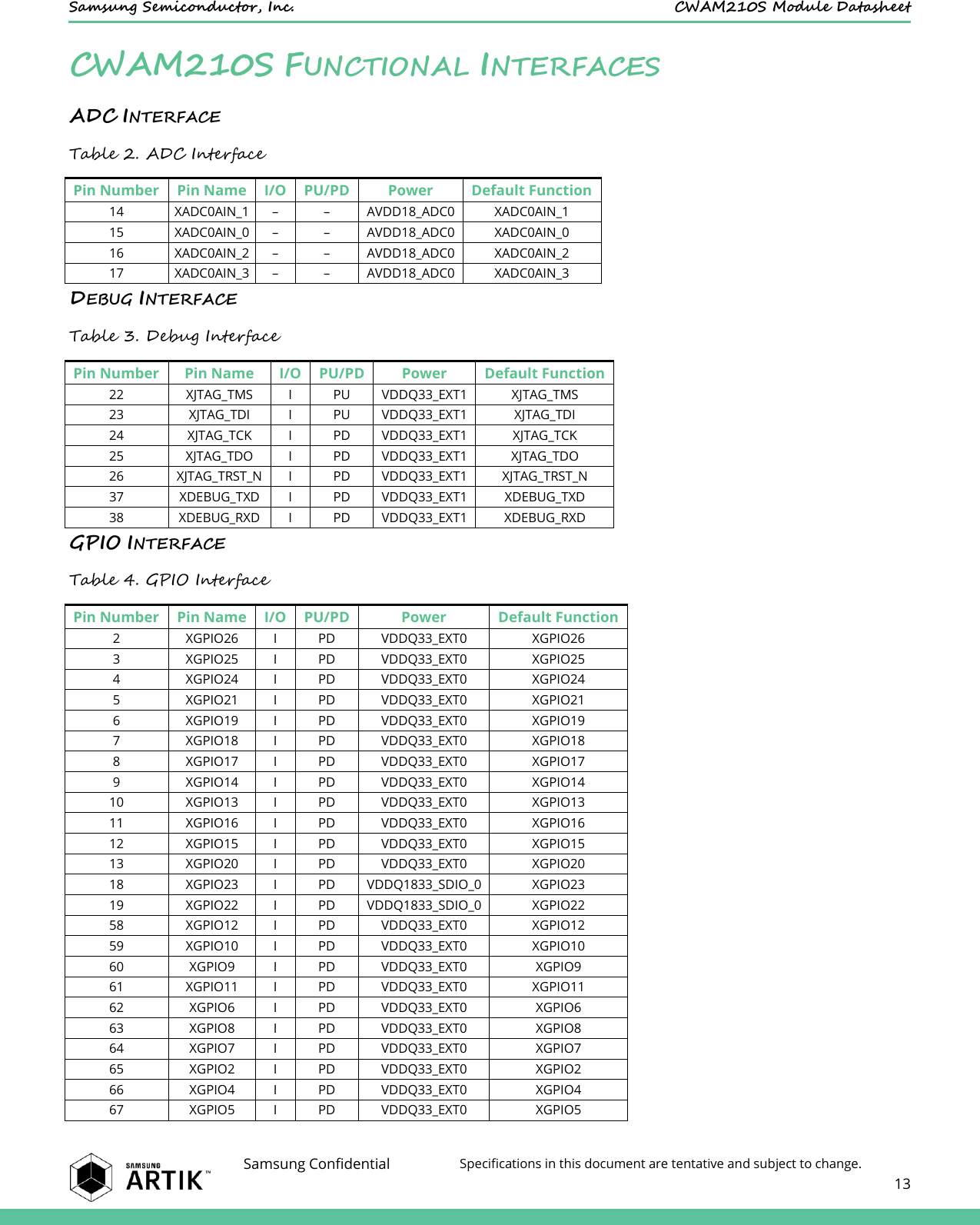
Samsung Electronics Co CWAM210S IOT Module User Manual Samsung ARTIK ation
Samsung Electronics Co Ltd IOT Module Samsung ARTIK ation
UserManual.wiki
>
Samsung Electronics Co
>
CWAM210S User Manual
Installation Manual
Navigation menu
Upload a User Manual
Namespaces
Wiki Guide
HTML
PDF
Info
Views
User Manual
Discussion / Help
Navigation
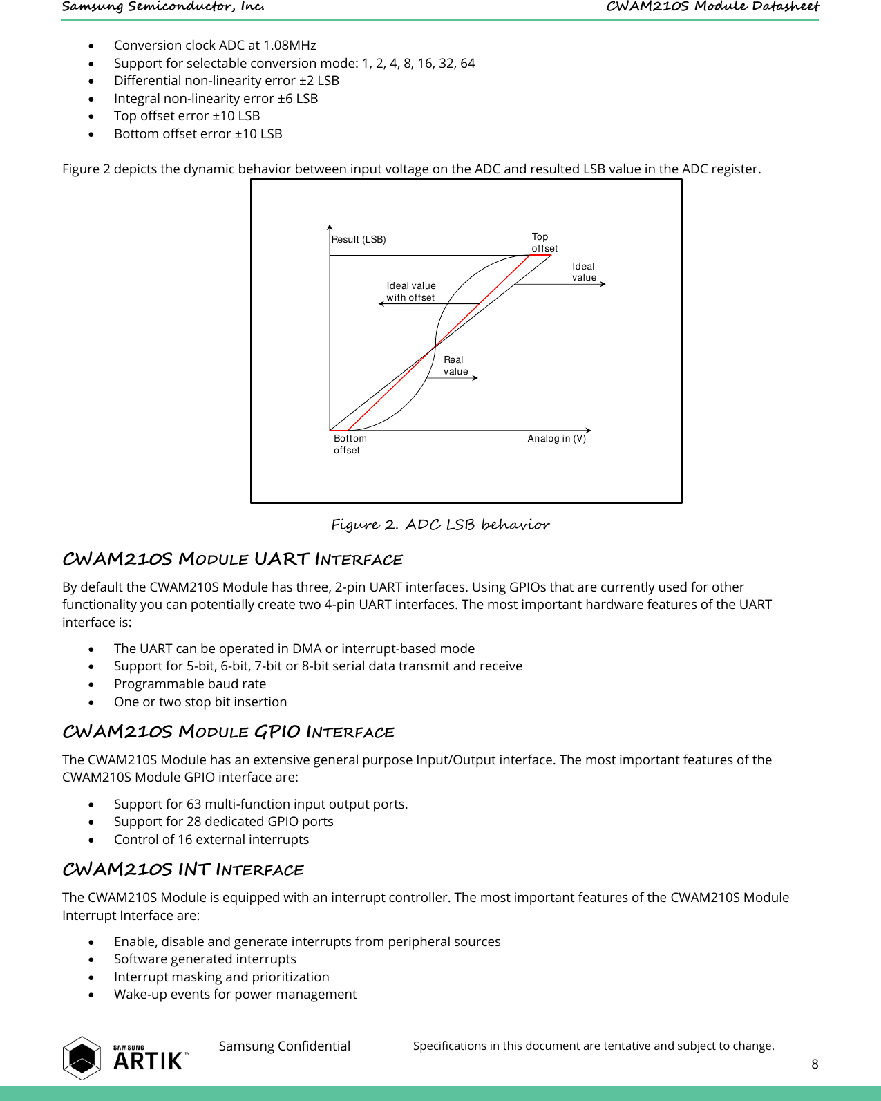
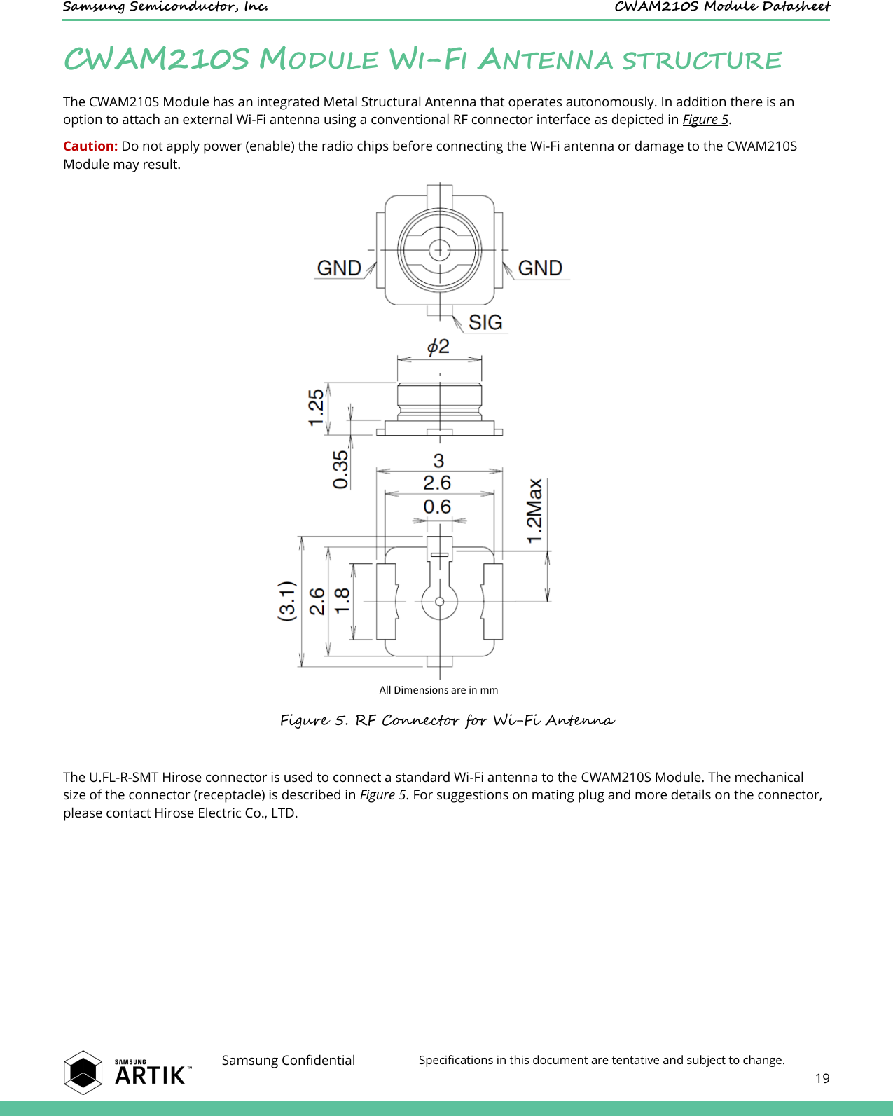
![Samsung Semiconductor, Inc. CWAM210S Module Datasheet Samsung Confidential Specifications in this document are tentative and subject to change. 4 LIST OF FIGURES Figure 1. CWAM210S Module Block Diagram ....................................................................................................................... 6 Figure 2. ADC LSB behavior .................................................................................................................................................... 8 Figure 3. CWAM210S Module Edge Connector ................................................................................................................. 10 Figure 4. Booting and Reset Timing Relations ................................................................................................................... 18 Figure 5. RF Connector for Wi-Fi Antenna .......................................................................................................................... 19 Figure 6. CWAM210S Module Mechanical Dimensions.................................................................................................... 23 LIST OF TABLES Table 1. CWAM210S Module Edge Connector Table Signal Descriptions...................................................................... 10 Table 2. ADC Interface .......................................................................................................................................................... 13 Table 3. Debug Interface ...................................................................................................................................................... 13 Table 4. GPIO Interface ......................................................................................................................................................... 13 Table 5. I2C Interface ............................................................................................................................................................. 14 Table 6. Interrupt Interface .................................................................................................................................................. 14 Table 7. PWM Interface......................................................................................................................................................... 14 Table 8. Reset Interface ........................................................................................................................................................ 14 Table 9. SPI Interface ............................................................................................................................................................ 15 Table 10. Level Shifter........................................................................................................................................................... 15 Table 11. UART Interface ...................................................................................................................................................... 15 Table 12. Alternate functions of the CWAM210S Module ............................................................................................... 16 Table 13. Absolute Maximum Ratings ................................................................................................................................ 20 Table 14. I/O DC Electrical Characteristics (PAD:[2-13,18,19],[21-26],[28-31],[33-45],[48-75], I/O) ............................ 20 Table 15. I/O DC Electrical Characteristics (PAD:[14-17], ADC) ........................................................................................ 20 Table 16. Recommended Operating Conditions ............................................................................................................... 21 Table 17. I/O Drive Strength ................................................................................................................................................ 21 Table 18. ESD Ratings ........................................................................................................................................................... 21 Table 19.Level Shifter AC Electrical Characteristics .......................................................................................................... 21](https://usermanual.wiki/Samsung-Electronics-Co/CWAM210S/User-Guide-3316615-Page-4.png)
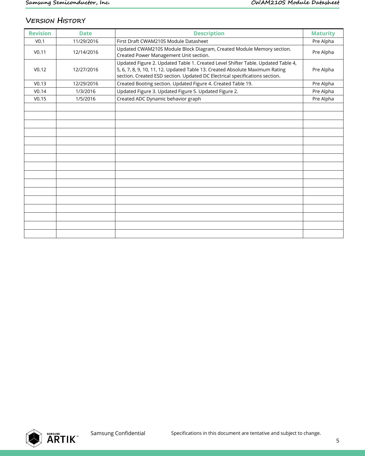
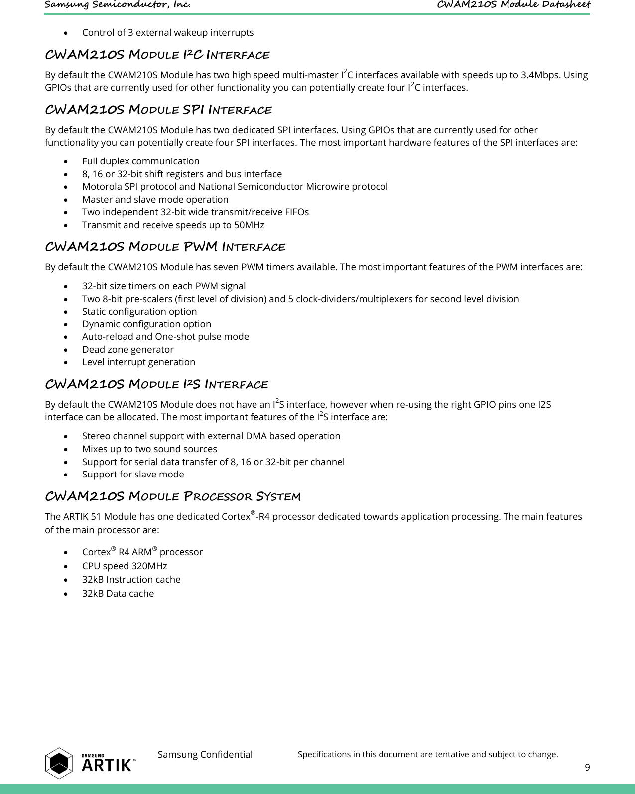
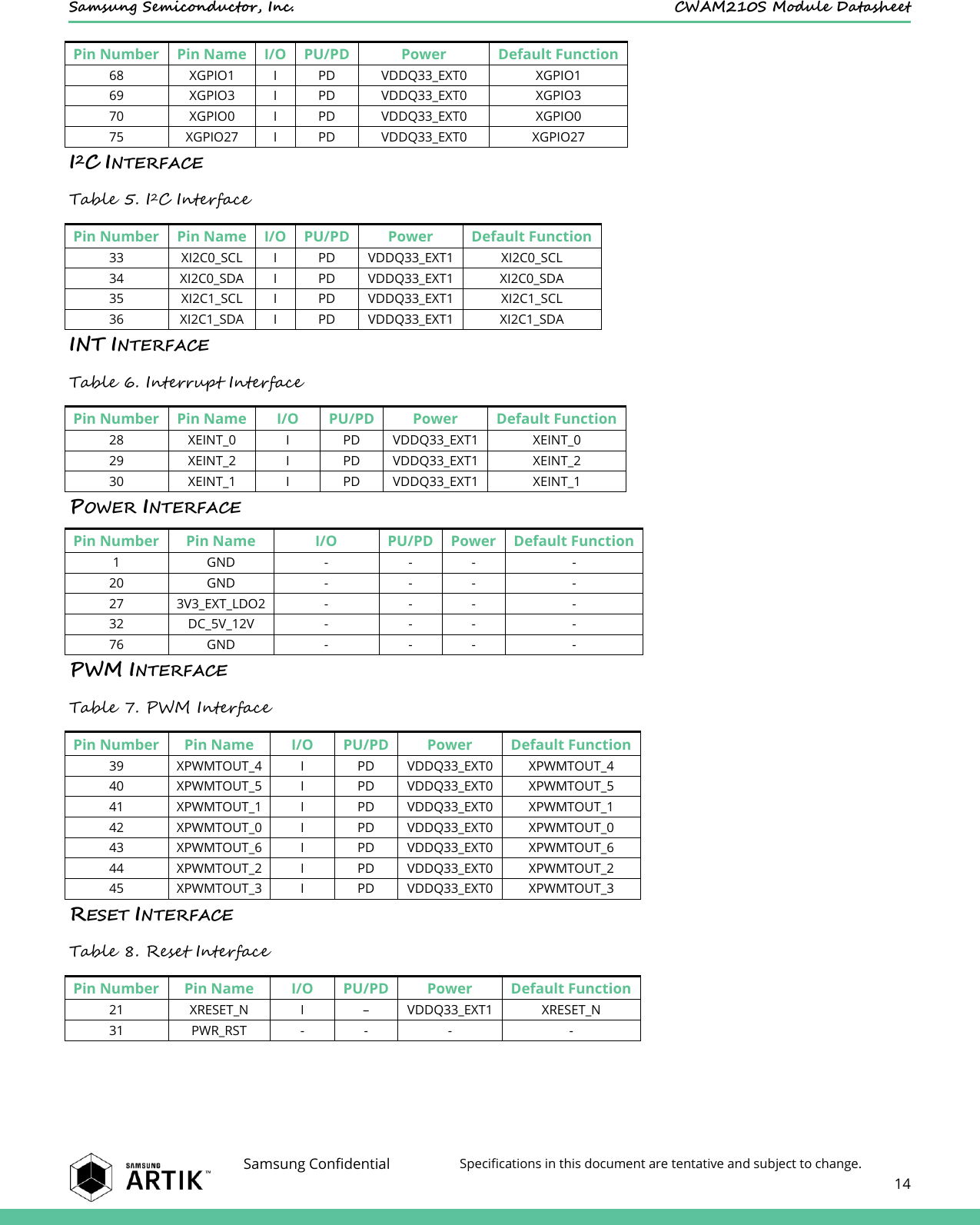
![Samsung Semiconductor, Inc. CWAM210S Module Datasheet Samsung Confidential Specifications in this document are tentative and subject to change. 12 Pin Number Pin Name I/O* PU/PD Power Default Function Groups 63 XGPIO8 I PD VDDQ33_EXT0 GPIO 63 64 XGPIO7 I PD VDDQ33_EXT0 GPIO 64 65 XGPIO2 I PD VDDQ33_EXT0 GPIO 65 66 XGPIO4 I PD VDDQ33_EXT0 GPIO 66 67 XGPIO5 I PD VDDQ33_EXT0 GPIO 67 68 XGPIO1 I PD VDDQ33_EXT0 GPIO 68 69 XGPIO3 I PD VDDQ33_EXT0 GPIO 69 70 XGPIO0 I PD VDDQ33_EXT0 GPIO 70 71 XSPI1_MISO I PD VDDQ33_EXT0 SPI 71 72 XSPI1_CLK I PD VDDQ33_EXT0 SPI 72 73 XSPI1_MOSI I PD VDDQ33_EXT0 SPI 73 74 XSPI1_CSN I PD VDDQ33_EXT0 SPI 74 75 XGPIO27 I PD VDDQ33_EXT0 GPIO 75 76 GND - - - GND 76 Note: 1. *Default setting after reset 2. Type definition: [S:Signal ball, P:Power ball, G:GND ball] 3. IO pad type definition: [I:Input, O:Output, I/O: Input/Output 4. Internal Pull Up/Down definition: – PU:Pull Up, PD:Pull Down, N:No Pull](https://usermanual.wiki/Samsung-Electronics-Co/CWAM210S/User-Guide-3316615-Page-12.png)
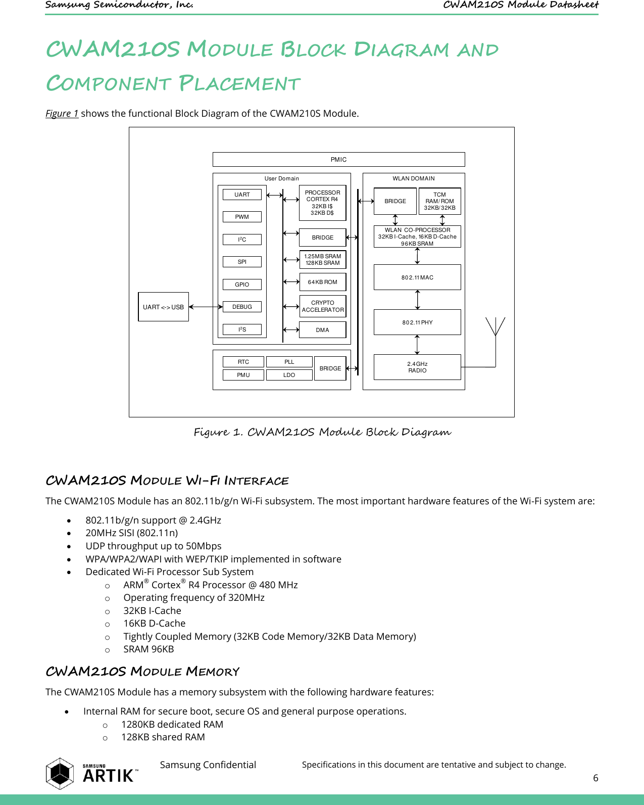
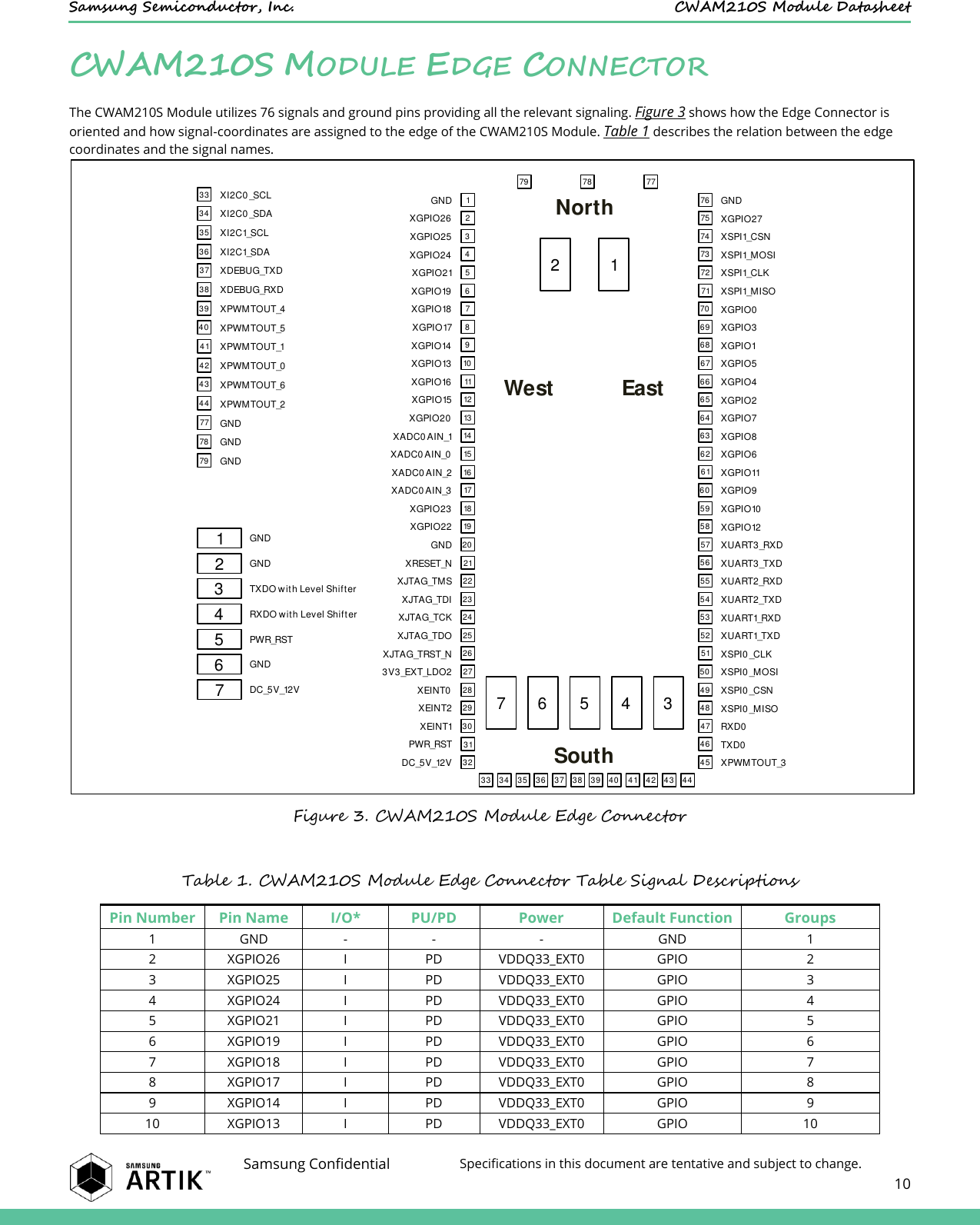
![Samsung Semiconductor, Inc. CWAM210S Module Datasheet Samsung Confidential Specifications in this document are tentative and subject to change. 16 CWAM210S MODULE GPIO ALTERNATE FUNCTIONS Table 12 describes the alternate functions that can be accessed using GPIOs that are available on the edge of the CWAM210S Module. Table 12. Alternate functions of the CWAM210S Module PIN # Pin Name Default Function Alternate Function 1 2 3 4 5 6 7 2 XGPIO26 XGPIO26 GPG3[2] I2S_0_SDO MCT1_INTlev - - - - 3 XGPIO25 XGPIO25 GPG3[1] I2S_0_LRCK MCT0_TICK - - - - 4 XGPIO24 XGPIO24 GPG3[0] I2S_0_BCLK MCT0_INTlev WB2AP_ETM_DATA_OUT_15 WLBT_DEBUG_15 - - 5 XGPIO21 XGPIO21 GPG2[5] SerialFLASH_MONITOR_sf1_5 WLBT_UART_TXD WB2AP_ETM_DATA_OUT_12 WLBT_DEBUG_12 WAKE_EXT_INTG2[5] - 6 XGPIO19 XGPIO19 GPG2[3] SerialFLASH_MONITOR_sf1_3 WB2AP_ETM_DATA_OUT_10 WLBT_DEBUG_10 WAKE_EXT_INTG2[3] - - 7 XGPIO18 XGPIO18 GPG2[2] SerialFLASH_MONITOR_sf1_2 WB2AP_ETM_DATA_OUT_09 WLBT_DEBUG_09 WAKE_EXT_INTG2[2] - - 8 XGPIO17 XGPIO17 GPG2[1] SerialFLASH_MONITOR_sf1_1 WB2AP_ETM_DATA_OUT_08 WLBT_DEBUG_08 WAKE_EXT_INTG2[1] - - 9 XGPIO14 XGPIO14 GPG1[6] SerialFLASH_MONITOR_sf0_6 ALV_DBG[14] WB2AP_ETM_DATA_OUT_05 WLBT_DEBUG_05 WAKE_EXT_INTG1[6] - 10 XGPIO13 XGPIO13 GPG1[5] SerialFLASH_MONITOR_sf0_5 ALV_DBG[13] WB2AP_ETM_DATA_OUT_04 WLBT_DEBUG_04 WAKE_EXT_INTG1[5] - 11 XGPIO16 XGPIO16 GPG2[0] SerialFLASH_MONITOR_sf1_0 WB2AP_ETM_DATA_OUT_07 WLBT_DEBUG_07 WAKE_EXT_INTG2[0] - - 12 XGPIO15 XGPIO15 GPG1[7] SerialFLASH_MONITOR_sf0_7 ALV_DBG[15] WB2AP_ETM_DATA_OUT_06 WLBT_DEBUG_06 WAKE_EXT_INTG1[7] - 13 XGPIO20 XGPIO20 GPG2[4] SerialFLASH_MONITOR_sf1_4 WLBT_UART_RXD WB2AP_ETM_DATA_OUT_11 WLBT_DEBUG_11 WAKE_EXT_INTG2[4] - 18 XGPIO23 XGPIO23 GPG2[7] SerialFLASH_MONITOR_sf1_7 WB2AP_ETM_DATA_OUT_14 WLBT_DEBUG_14 WAKE_EXT_INTG2[7] - - 19 XGPIO22 XGPIO22 GPG2[6] SerialFLASH_MONITOR_sf1_6 WB2AP_ETM_DATA_OUT_13 WLBT_DEBUG_13 WAKE_EXT_INTG2[6] - - 22 XJTAG_TMS XJTAG_TMS ETC0[1] - - - - - - 23 XJTAG_TDI XJTAG_TDI ETC0[3] - - - - - - 24 XJTAG_TCK XJTAG_TCK ETC0[2] - - - - - - 25 XJTAG_TDO XJTAG_TDO ETC0[4] - - - - - - 26 XJTAG_TRST_N XJTAG_TRST_N ETC0[0] - - - - - - 28 XEINT_0 XEINT_0 GPA0[0] WAKE_EXT_INTA0[0] - - - - - 29 XEINT_2 XEINT_2 GPA0[2] WAKE_EXT_INTA0[2] - - - - - 30 XEINT_1 XEINT_1 GPA0[1] WAKE_EXT_INTA0[1] - - - - - 33 XI2C0_SCL XI2C0_SCL GPA1[0] HSI2C_0_SCL - - - - - 34 XI2C0_SDA XI2C0_SDA GPA1[1] HSI2C_0_SDA - - - - - 35 XI2C1_SCL XI2C1_SCL GPA1[2] HSI2C_1_SCL - - - - - 36 XI2C1_SDA XI2C1_SDA GPA1[3] HSI2C_1_SDA - - - - - 37 XDEBUG_TXD XDEBUG_TXD GPA3[1] Xdebug_TXD - - - - - 38 XDEBUG_RXD XDEBUG_RXD GPA3[0] Xdebug_RXD - - - - - 39 XPWMTOUT_4 XPWMTOUT_4 GPP2[4] PWM_TOUT_4 - - - - - 40 XPWMTOUT_5 XPWMTOUT_5 GPP2[5] PWM_TOUT_5 - - - - - 41 XPWMTOUT_1 XPWMTOUT_1 GPP2[1] PWM_TOUT_1 COUNTER_0 UART_3_RTSn - - -](https://usermanual.wiki/Samsung-Electronics-Co/CWAM210S/User-Guide-3316615-Page-16.png)
![Samsung Semiconductor, Inc. CWAM210S Module Datasheet Samsung Confidential Specifications in this document are tentative and subject to change. 17 PIN # Pin Name Default Function Alternate Function 1 2 3 4 5 6 7 42 XPWMTOUT_0 XPWMTOUT_0 GPP2[0] PWM_TOUT_0 UART_3_CTSn - - - - 43 XPWMTOUT_6 XPWMTOUT_6 GPP2[6] PWM_TOUT_6 - - - - - 44 XPWMTOUT_2 XPWMTOUT_2 GPP2[2] PWM_TOUT_2 - - - - - 45 XPWMTOUT_3 XPWMTOUT_3 GPP2[3] PWM_TOUT_3 - - - - - 48 XSPI0_MISO XSPI0_MISO GPP0[2] SPI_0_MISO - - - - - 49 XSPI0_CSN XSPI0_CSN GPP0[1] SPI_0_CSn - - - - - 50 XSPI0_MOSI XSPI0_MOSI GPP0[3] SPI_0_MOSI - - - - - 51 XSPI0_CLK XSPI0_CLK GPP0[0] SPI_0_CLK - - - - - 52 XUART1_TXD XUART1_TXD GPP0[5] UART_1_TXD UART_2_RTSn - - - - 53 XUART1_RXD XUART1_RXD GPP0[4] UART_1_RXD UART_2_CTSn - - - - 54 XUART2_TXD XUART2_TXD GPP0[7] UART_2_TXD - - - - - 55 XUART2_RXD XUART2_RXD GPP0[6] UART_2_RXD - - - - - 56 XUART3_TXD XUART3_TXD GPP1[7] UART_3_TXD - - - - - 57 XUART3_RXD XUART3_RXD GPP1[6] UART_3_RXD - - - - - 58 XGPIO12 XGPIO12 GPG1[4] SerialFLASH_MONITOR_sf0_4 ALV_DBG[12] WB2AP_ETM_DATA_OUT_03 WLBT_DEBUG_03 WAKE_EXT_INTG1[4] - 59 XGPIO10 XGPIO10 GPG1[2] SPI_3_MISO SerialFLASH_MONITOR_sf0_2 ALV_DBG[10] WB2AP_ETM_DATA_OUT_01 WLBT_DEBUG_01 WAKE_EXT_INTG1[2] 60 XGPIO9 XGPIO9 GPG1[1] SPI_3_CSn SerialFLASH_MONITOR_sf0_1 ALV_DBG[9] WB2AP_ETM_DATA_OUT_00 WLBT_DEBUG_00 WAKE_EXT_INTG1[1] 61 XGPIO11 XGPIO11 GPG1[3] SPI_3_MOSI SerialFLASH_MONITOR_sf0_3 ALV_DBG[11] WB2AP_ETM_DATA_OUT_02 WLBT_DEBUG_02 WAKE_EXT_INTG1[3] 62 XGPIO6 XGPIO6 GPG0[6] SPI_2_MISO ALV_DBG[6] - - - - 63 XGPIO8 XGPIO8 GPG1[0] SPI_3_CLK SerialFLASH_MONITOR_sf0_0 ALV_DBG[8] WB2AP_TRACE_CLK_OUT WAKE_EXT_INTG1[0] - 64 XGPIO7 XGPIO7 GPG0[7] SPI_2_MOSI ALV_DBG[7] - - - - 65 XGPIO2 XGPIO2 GPG0[2] HSI2C_3_SCL ALV_DBG[2] - - - - 66 XGPIO4 XGPIO4 GPG0[4] SPI_2_CLK ALV_DBG[4] - - - - 67 XGPIO5 XGPIO5 GPG0[5] SPI_2_CSn ALV_DBG[5] - - - - 68 XGPIO1 XGPIO1 GPG0[1] HSI2C_2_SDA ALV_DBG[1] - - - - 69 XGPIO3 XGPIO3 GPG0[3] HSI2C_3_SDA ALV_DBG[3] - - - - 70 XGPIO0 XGPIO0 GPG0[0] HSI2C_2_SCL ALV_DBG[0] - - - - 71 XSPI1_MISO XSPI1_MISO GPP4[2] SPI_1_MISO - - - - - 72 XSPI1_CLK XSPI1_CLK GPP4[0] SPI_1_CLK - - - - - 73 XSPI1_MOSI XSPI1_MOSI GPP4[3] SPI_1_MOSI - - - - - 74 XSPI1_CSN XSPI1_CSN GPP4[1] SPI_1_CSn - - - - - 75 XGPIO27 XGPIO27 GPG3[3] I2S_0_SDI MCT1_TICK - - - -](https://usermanual.wiki/Samsung-Electronics-Co/CWAM210S/User-Guide-3316615-Page-17.png)
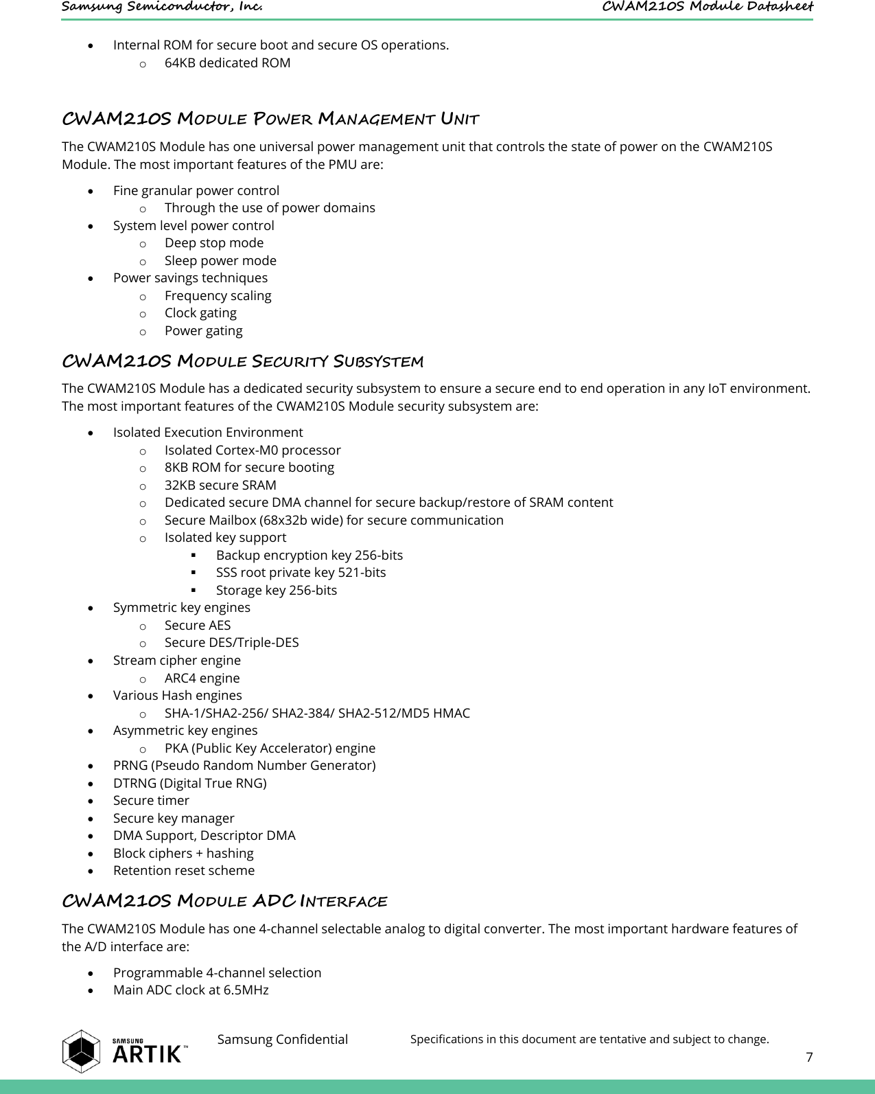
![Samsung Semiconductor, Inc. CWAM210S Module Datasheet Samsung Confidential Specifications in this document are tentative and subject to change. 20 CWAM210S MODULE ELECTRICAL SPECIFICATIONS ABSOLUTE MAXIMUM RATING Table 13. Absolute Maximum Ratings PAD:[Pin#] Symbol Condition Min Typ Max Units PAD:[32] VIN Input voltage VIN on the high efficiency step down converter – – 20 V PAD:[2~19], [21~26], [28~31], [33~45], [48~75] Vundershoot Undershoot voltage for I/O -0.3 – - V PAD:[31] PWR_RST – -0.3 – 6 V PAD:[46,47] VMAX Based on 3V3 I/O signalling – – 63.3 V IMAX Continuous – – 305 mA Pulsed – – 800 mA DC ELECTRICAL CHARACTERISTICS Table 14. I/O DC Electrical Characteristics (PAD:[2-13,18,19],[21-26],[28-31],[33-45],[48-75], I/O) Parameter Condition Min Typ Max Units Tolerant External Voltage VTOL 3.3 Power Off and On – – 3.60 V High-Level Input Voltage CMOS Interface VIH 2.31 – 3.60 V Low-Level Input Voltage CMOS Interface VIL VDD=3.30V -0.30 – 0.70 V Hysteresis Voltage ΔV 0.15 – – V High-Level Input Current Input Buffer IIH VIN=3.30V VDD=3.30V Power On -3.00 – 3.00 µA VDD=3.30V Power Off & SNS=0 -5.00 – 5.00 µA Input Buffer with Pull-Down VIN=3.30V VDD=3.30V 13 40 90 µA Low-Level Input Current Input Buffer IIL VIN=0V VDD=3.30V Power On and Off -3.00 – 3.00 µA Input Buffer with Pull-Down VIN=0V VDD=3.30V -13.00 – -90.00 µA Output High Voltage VOH IOH = 2.0mA, 4.0mA, 8.0mA and 12.0mA 2.64 – 3.30 V Output Low Voltage VOL IOL = -2.0mA, -4.0mA, -8.0mA and -12.0mA 0 – 0.66 V Output Hi-Z Current VOZ -5 – 5 µA Input Capacitance CIN Any input and bi-directional buffers – – 5 pF Table 15. I/O DC Electrical Characteristics (PAD:[14-17], ADC) Parameter Condition Min Typ Max Units High Level Input Voltage VIH Guaranteed Logic High Level 1.26 – 1.80 V Low Level Input Voltage VIL Guaranteed Logic Low Level 0 – 0.54 V Output High Voltage VOH IOH=2mA, 4mA, 8mA and 12mA 1.44 – 1.80 V Output Low Voltage VOL IOL=2mA, 4mA, 8mA and 12mA 0 – 0.36 V Input Pull-Up Resistor Current IRPU VPAD=0 15 – 77 µA Input Pull-Down Resistor Current IRPD VPAD=1.80 17 – 77 µA](https://usermanual.wiki/Samsung-Electronics-Co/CWAM210S/User-Guide-3316615-Page-20.png)
![Samsung Semiconductor, Inc. CWAM210S Module Datasheet Samsung Confidential Specifications in this document are tentative and subject to change. 21 Parameter Condition Min Typ Max Units Input Hysteresis VH – 0.18 – – V Input Leakage Current for Non Tolerant Cells IPAD DVDD=1.80, VPAD=0 or 1.80V -6 – +6 µA Off State Leakage Current IOZ DVDD=1.80, VPAD=0 or 1.80V -6 – +6 µA Table 16. Recommended Operating Conditions Parameter Symbol Min Typ Max Units Main Power Supply: PAD:[32] DC_5V_12V 4.50 – 18.00 V Maximum Operating Temperature TO -20 – 70 °C Storage Temperature TS TBD – TBD °C Table 17. I/O Drive Strength State Currents: worst conditions VDD=3.30V Units DS0 DS1 SR: 0: Fast, 1: Slow 0 0 0/1 2 mA 0 1 0/1 4 mA 1 0 0/1 8 mA 1 1 0/1 12 mA DC MODULE USE CASE CHARACTERISTICS TBD POWER SUPPLY REQUIREMENTS TBD ESD RATINGS Table 18. ESD Ratings Parameter Min Typ Max Units ESD stress voltage Human Body Model (JEDEC) -1.0 – 1.0 kV ESD stress voltage Charged Device Model – 250 – V AC ELECTRICAL CHARACTERISTICS Table 19.Level Shifter AC Electrical Characteristics PAD:[Pin#] Symbol Condition Min Typ Max Units PAD:[46,47] Dynamic Characteristics CISS Input Capacitance VDS=25V, f=1.0MHz, VGS=0V – – 50 pF COSS Output Capacitance – – 25 pF CRSS Reverse Transfer Capacitance – – 5 pF RF ELECTRICAL CHARACTERISTICS TBD](https://usermanual.wiki/Samsung-Electronics-Co/CWAM210S/User-Guide-3316615-Page-21.png)

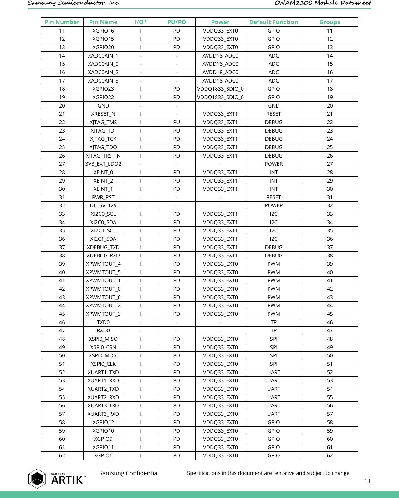
![Samsung Semiconductor, Inc. CWAM210S Module Datasheet Samsung Confidential Specifications in this document are tentative and subject to change. 23 CWAM210S MODULE MECHANICAL SPECIFICATIONS In Figure 6 the mechanical dimensions of the CWAM210S Module are provided. All dimensions are in mm. Figure 6. CWAM210S Module Mechanical Dimensions 0.65NorthWest EastSouthNorthSouth764544 33TOP View BOTTOM View1.65 1.651232.54 72.426.231.22.543.77.577 790.41.0Solder plate(bottom side only)0.60.61.00.27.731.74.754.01540All Dimensions in [mm]11.311.728.532.45321East West](https://usermanual.wiki/Samsung-Electronics-Co/CWAM210S/User-Guide-3316615-Page-23.png)