Samsung Electronics Co WIDT10B WLAN Module User Manual WiDT10B Manual 101129
Samsung Electronics Co Ltd WLAN Module WiDT10B Manual 101129
Users Manual
DNUB-S2
M
O
D
E
S
S
A
Green
P
Vendor
Registr
a
A TE
R
Indemn
WNC
w
directo
r
liabilit
y
profess
i
Compo
n
propert
y
intellec
t
Compo
n
copyrig
h
Samsu
n
or mod
i
infringi
n
ITEM
O
DEL NA
M
E
SCRIPTI
O
S
OLUTIO
N
A
MSUNG P
WNC P/N
P
rocurement
Code
a
tion Date
DRAWIN
G
R
M OF VA
L
ification
w
ill indemni
f
r
s, officers,
e
y
or expense
i
onals) arisi
n
n
ents provi
d
y
right. If
W
t
ual propert
y
n
ents provi
d
h
t or trade s
n
g the right t
o
i
fy the alleg
e
n
g item.
MAKER
ADDRESS
U
M
E
O
N
N
/N
G
L
IDITY
f
y, hold har
m
e
mployees,
a
( including
c
n
g out of or
r
d
ed by WN
C
W
NC receiv
e
y
right infri
n
d
ed by WN
C
e
cret infrin
g
o
continued
u
e
dly infringi
n
2
0
U
se
r
CHECK
OVER
A
m
less, and a
t
a
gents and i
n
c
ourt costs
a
r
esulting fr
o
C
infringes p
a
e
s notice of
a
n
gement or i
f
C
shall be pr
e
g
ement, WN
C
u
se of the P
r
n
g item suc
h
WNC
0
Park Ave
n
r
ma
n
US
B
IEEE 8
Bro
a
A
G
A
T LEAST
1
t
Samsung's
n
dependent
c
a
nd reasona
b
o
m any third
a
tent, copyr
i
a
n alleged p
a
f
Samsung's
e
vented by p
C
may, at it
s
r
oducts and/
o
h
that it is no
n
ue II, Hsinc
h
n
ua
l
B
Embedde
d
WIDT10B
02.11n 2x2
W
a
dcom: BC
M
BN59-011
3
G
REEMEN
T
1
5-YEARS
request, de
f
c
ontractors f
r
b
le fees of a
t
party claim
i
ght, trade s
e
a
tent, copyri
use of the
P
ermanent in
j
s
sole optio
n
o
r the Com
p
longer infri
n
TEL
h
u Science
P
l
d
Module
B
W
iFi Mode
M
43236
3
0A
T
FROM IS
S
f
end Samsu
n
r
om and aga
t
torneys and
that any Pr
o
e
cret right o
r
ght, trade s
e
P
roducts and
/
j
unction for
n
and expen
s
p
onents as p
r
n
ging, or re
p
8
P
ark, Hsinc
h
APPROV
A
S
UED DAT
E
n
g and Sams
u
inst any los
s
other
o
ducts and/
o
r
other intell
e
cret or othe
r
/
or the
reasons of
p
s
e, procure
fo
r
ovided here
u
p
lace the all
e
8
86-3-6667
7
h
u 308, Tai
w
A
L
E
u
ng's
s
, cost,
o
r
ectual
r
p
atent,
fo
r
u
nder,
e
gedly
7
99
w
an
D
I
D
NUB-S2
I
ndex
Part I
_
1.
2.
3.
4.
5.
Part I
I
1. In
t
2. Fe
3. H
a
3
4. L
a
5. P
C
5
6. Sp
6
6
6
6
6
7. M
F
8. In
s
_
Genera
l
History S
h
Part List
Circuit dia
g
PCBA pi
c
Box packa
g
I_
Specifi
c
t
roduction
atures
a
rdware Arc
h
3
.1 Mai
n
a
bel
C
B
5
.1 PC
B
ecifications
:
6
.1 Sup
p
6
.2 Cur
r
6
.3 RF
p
6
.4 RF
S
6
.5 Env
i
F
G test ite
m
s
tallation Pr
o
l
informat
h
eet
g
ram
c
ture
g
e spec
c
ation of
W
h
itecture:
n
Chipset In
f
B
Gerbe
r
:
p
ly Voltage
r
ent Consu
m
p
owe
r
S
ensitivity
i
ronmental
S
m
s
o
cedure
ion
W
IDT10
B
f
ormation
m
ption
S
pec
B

DNUB-S2
1. Re
v
Edi
t
V
V
v
ision Hi
s
t
ion # R
e
0.1 In
i
0.2 In
i
(
2
s
tory
e
ason for re
v
i
tial Draft
D
i
tial Draft
D
2
010/10/06
v
v
ision
D
ocument
b
a
s
D
ocument
b
v
ersion)
s
e on Sams
u
ase on Sa
m
u
ng V0.2 H
D
m
sung V0.4
1
DK
1
HDK
Issue date
2010/09/1
0
2010/10/1
5
0
5
2
3
DNUB-S2
2
. Part li
s
36
C3,C28,C32,C6
5
9
4 2 C13,C16
5 2 C17,C27
61C18
7 3 C19,C86,C87
819
C21,C22,C24,C
2
31,C33,C34,C4
0
,C51,C53,C69,
C
82,C84,C88
9 2 C23,C30
10 6 C37,C38,C44,C
5
11 1 C39
12 2 C41,C58
13 1 C42
14 6 C62,C74,C75,C
7
85
15 5 C63,C76,C78,C
8
16 1 CN1
17 4 C120,C130,C14
18 1 BD1
19 1 BD2
20 2 L1,L2
21 6 R20,R27,R42,R
4
53
22 1 R1
23 6 R16,R17,R18,R
34
24 1 R7
25 1 R24
26 1 R40
27 1 R29
28 2 R30,R32
29 1 R31
30 3 R33,R61,R62
31 1 R35
32 1 R50
33 1 D1
34 2 U3,U4
35 1 IC5
36 1 X1
97
A1
37 1 IC1
3
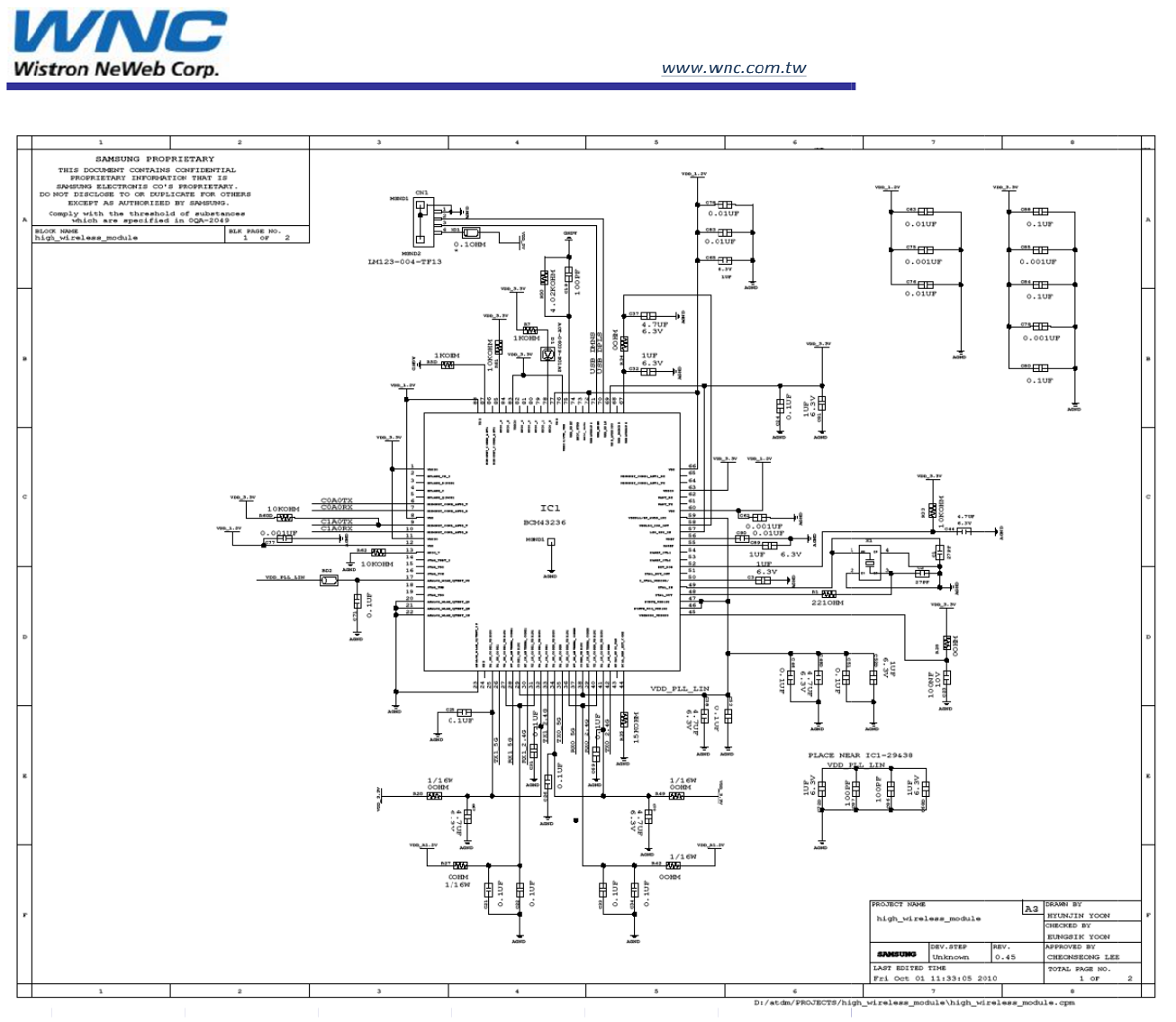
. Circui
t
s
t
5
,C81,C8 1uF
9pF
4.7uF
0.1uF
100pF
2
5,C26,C
0
,C43,C46
C
71,C80,C 0.1uF
0.1uF
5
4,C67,C 4.7uF
39pF
10uF
22pF
7
7,C79,C 1000pF
8
3,C90 0.01uF
0,C150 9pF
2.2uH
4
3,R49,R 0
221
19,R28,R 0
1K
100K
100K
60.4K
59K
267K
10K
15K
4.02K
LED
20MHz
PCB
Shield Can
Antenna
BCM43236KMLG
t
diagra
m
CAP,CER,0402,1UF
CAP,CER,0402,9PF
CAP,CER,1206,4.7
U
CAP,CER,0603,0.1
U
CAP,CER,0201,100
P
CAP,CER,0201,0.1
U
CAP,CER,0402,0.1
U
CAP,CER,0603,4.7
U
CAP,CER,0201,39P
F
CAP,CER,0805,10U
CAP,CER,0201,22P
F
CAP,CER,0201,100
0
CAP,CER,0201,0.01
BOX,4P,1R,1.25mm
CAP,CER,0201,9PF
220ohm,2012,TP,80
o
600ohm,0402, 300m
2.2uH, ±20%, 0.158
Ω
RES,THK,0402,0,5
%
RES,THK,0201,221,
RES,THK,0201,0,5
%
RES,THK,0201,1K,
5
RES,THK,0201,100
K
RES,THK,0402,100
K
RES,THK,0402,60.4
RES,THK,0402,59K,
RES,THK,0402,267
K
RES,THK,0201,10K,
RES,THK,0201,15K,
RES,THK,0201,4.02
SMD,BLUE,1.6x0.8
x
MOD,SMT,2.4-2.5/4
.
IC,REG,WDFN12,A
D
XTL,FXD,SMT,20.0
0
34x36mm, 4Layer,
T
Carrier type
WLAN SINGLE CHI
P
m
,10%,6.3V,X6S,X5R
,0.25PF,50V,NP0,C0G
U
F,20_80%,25V,Y5V
U
F,80_20%,50V,Y5V
P
F,5%,25V,X7R
U
F,10%,6.3V,X5R
U
F,10%,10V,X5R
U
F,20%,6.3V,X5R
F
,5%,16V,NP0,C0G
F,10%,10V,X5R
F
,5%,25V,NP0,C0G
0
PF,10%,25V,X7R
UF,10%,6.3V,X5R
,SMD-A,Sn,2um min,NATUR
A
,0.5PF,25V,NP0
o
hm/100MHz,200ohm/600M
H
A, 0.6ohm
Ω
1.4A, 2.5X2mm
%
,63MW 50V
1%,50MW
%
,50MW
5
%,50MW
K
,5%,50MW
K
,5%,50MW
K,1%,63MW
1%,63MW
K
,1%,63MW
5%,50MW
1%,50MW
K,1%
x
0.4mm,470,1.6x0.8x0.4mm
.
9-5.875GHZ,3.3V,3X3X1M
M
D
J_ADJ,1_1A,SW,1.5MHZ,B
U
0
0MHZ,10PPM,3.2X2.5X0.6
M
T
hrough hole via, Au plating
P
11N 2X2 -DUAL BAND
Rest BOM T
o
A
L
H
z
M
,SW/2DIPLEXER,802.11A/B
/
U
CK,UVL,SCP
M
M,9PF,FUND
o
tal
MURATA
SEM
TDK
YAGEO
SEM
MURATA
SEM
TDK
MURATA
MURATA
YAGEO
SEM
VENKEL
SEM
MURATA
TDK
SEM
TDK
SEM
MURATA
YAGEO
SEM
TDK
TDK
YAGEO
MURATA
SEM
TDK
YEONHO
A
DCOELECTR
O
FOOSUNG TEC
H
JAEEUN
ELECTRONICS
JWT
MURATA
SEM
MURATA
TDK
MATSUSHITA
YAGEO
ABCO
KOA
KOA
YAGEO
SEM
KOA
SEM
KOA
SEM
KOA
A
BCO
SEM
SEM
KOA
MATSUE ,PSIN
D
SEM
ROHM
KOA
SEM
YAGEO
ROHM
KOA
SEM
KOA
SEM
KOA
SEM
KOA
A
OT
LITE-ON SEMIC
O
SB1314E-V
/
G FEM TDK
SiGe
PAM
AURA micro
SEIKO EPSON
BROADCOM
GRM155R60J105K
E
CL05A105KQ5NNN
C
C1005X5R0J105K
CC0402KRX5R5BB
1
CL05C090CB5ANN
C
GJM1555C1H9R0C
B
CL31F475ZONE
C3216Y5V1E475Z
GRM188F51H104Z
A
GRM0335C1E101J
C0201KRX5R5BB1
0
CL03A104KQ3NNN
C
C0201X5R6R3-104
K
CL05A104KP5NNN
C
GRM155R61A104K
A
C1608X5R0J475MT
CL03C390JA3ANN
C
C0603C0G1E390JT
CL21A106KPFNNN
E
GRM21BR61A106K
E
C0201JRNP08BN22
CL03C220JA3ANN
C
C0603C0G1E220JT
C0603X7R1E102KT
C0201KRX7R8BB1
0
GRM033R60J103K
CL03A103KQ3NNN
H
C0603X5R0J103KT
O
NICS
H
12507WR-04L
LM123-004-TF13
FW12501-04
JE204-B1.25-5T4
A
1255WRO-4PS-H
K
IP125-L04B-C26
GRM0335C1E9R0D
D
CIC21P221NE
BLM15AG601SN1
VLS252010T-2R2M
ERJ2GEJ000X
RC0402JR-070R
ACR0402T000J
RK73Z1ETQTP
RK73H1HTQTB221
0
RC0201FR-07221R
RC0603J000CS
RK73Z1HTQTB
RC0603J102CS
RK73B1HL102J
RC0603J104CS
RK73B1HL104J
A
CR0402T104J
RC1005J104CS
RC1005F6042CS
RK73H1ETTP6042F
D
ERJ2RKF5902X
RC1005F5902CS
MCR01MZPF5902
RK73H1ETTP5902F
RC1005F2673CS
RC0402FR-07267K
MCR01MZPF2673
RK73H1ETTP2673F
RC0603J103CS
RK73B1HL103J
RC0603F153CS
RK73H1HTTB1502F
RC0603F4021CS
RK73H1HTTB4021F
O
N
A
OT-0603P-B01AZ
LIST-C193ZBKT-AC
광전자㈜
A
SM3053755T-5104
SE2577
PAM2306AYPAA
AUR9707
TSX-3225
IMP43236A0KMLG
S
E
19D
C
1
05
C
B
01J
A
01C
0
4
C
K
NP
C
A
01D
C
E
E
19L
0
C
0
2
H
K
D
01D
0
F
S
MIC
DNUB
-
-
S2
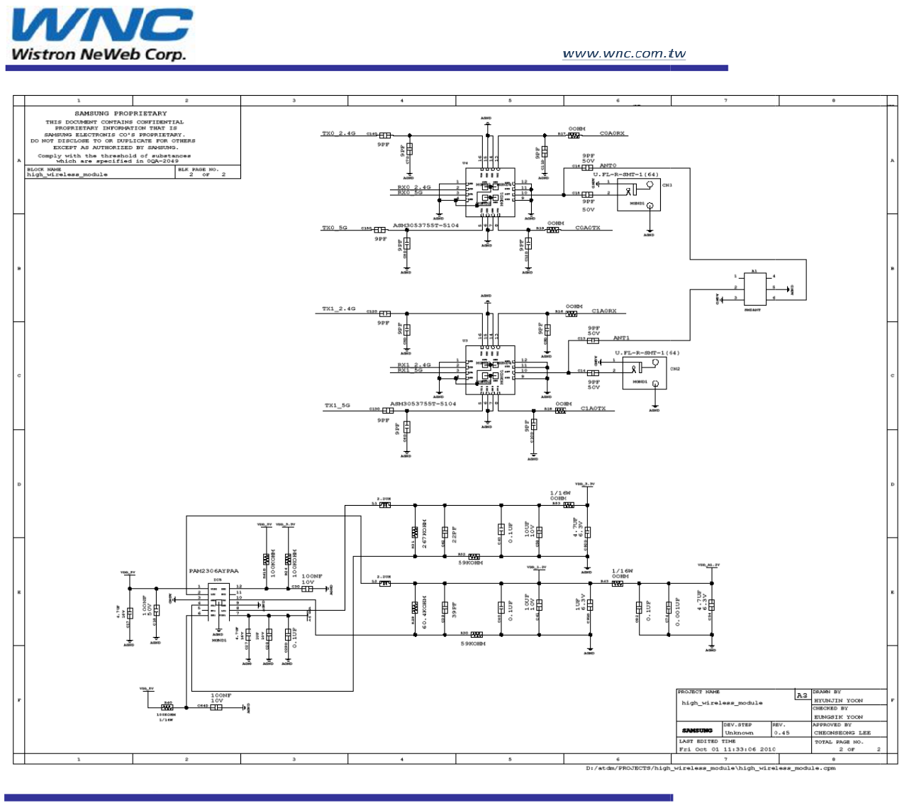
D
N
N
UB-S2
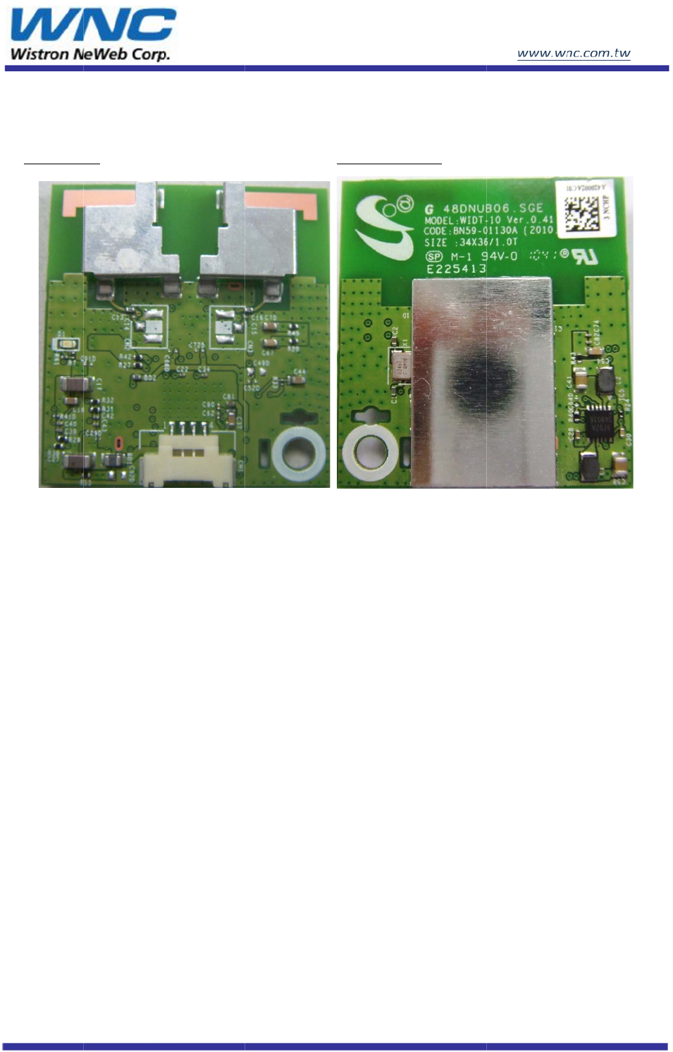
D
4
D
NUB-S2
4
. PCB
A
Top vie
w
5. Box
TBD
A
picture
w
Packag
e
e
Specifi
c
c
ation
Bottom
V
V
iew

P
1
2
DNUB-S2
P
art II
_
1
. Intro
d
D
N
core c
h
2
. Featu
r
2x
2
D
a
D
e
In
t
W
P
F
u
In
t
si
n
S
u
L
E
_
Specif
i
d
uction
N
UB-S2 is a
h
ipset is fro
m
r
es
2
a/b/g/n M
I
a
ta rates up
t
e
signs meet
P
t
egrated AR
M
P
A™/WPA
2
u
ll-rate AES
t
egrated 2.4
/
n
gle-
b
and d
e
u
pport for W
i
E
D reserved
i
cation
USB embe
d
m
Broadco
m
I
MO techno
l
o 130Mbps
P
b-free/Ro
H
M
® Cortex-
2
™
engine in h
a
/
5 GHz Pow
e
e
signs
i
ndows® X
P
for special
a
d
ded modul
e
m
, part numb
e
l
ogy
for 20MHz
c
H
S worldwi
d
M3™ CPU
a
rdware
e
r Amplifie
r
P
, Windows
V
a
pplication.
e
compliant
w
e
r BCM432
3
c
hannels an
d
d
e requirem
e
core plus 2
5
r
(BCM432
3
V
ista®, and
w
ith IEEE8
0
3
6.
d
300Mbps
f
e
nts
5
6KB ROM
3
6) provides
Linux® O
p
0
2.11n Draf
t
f
or 40MHz
c
and 448KB
path to low
e
p
erating Sys
t
t
2.0 standar
d
c
hannels
RAM
e
r solution
c
t
ems
d
. The
c
ost for

3
DNUB-S2
3
. Hard
w
3.1 M
a
I
t
M
A
w
are Arc
h
a
in Chips
e
t
em
A
C/BBP/R
a
h
itectur
e
e
t Inform
a
a
dio Transc
e
e
:
a
tion
e
iver/PA
Vende
r
Broadc
o
r
o
m
Part n
u
BCM
4
u
mber
4
3236
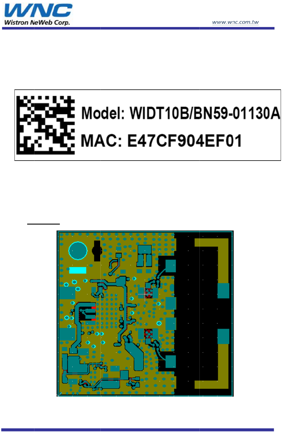
D
4
5
D
NUB-S2
4
. Label
Colo
r
Dime
n
PS: Th
i
5
. PCB
5.1 P
C
T
o
r
: White
n
sion : 30.
7
i
s is for pil
o
C
B Gerbe
r
o
p la
y
er
7
x9.3 m
m
o
t run samp
r
m
les onl
y
, th
e
e
final version waitin
g
f
f
or Samsu
n
ng
’s confir
m
m
ation.
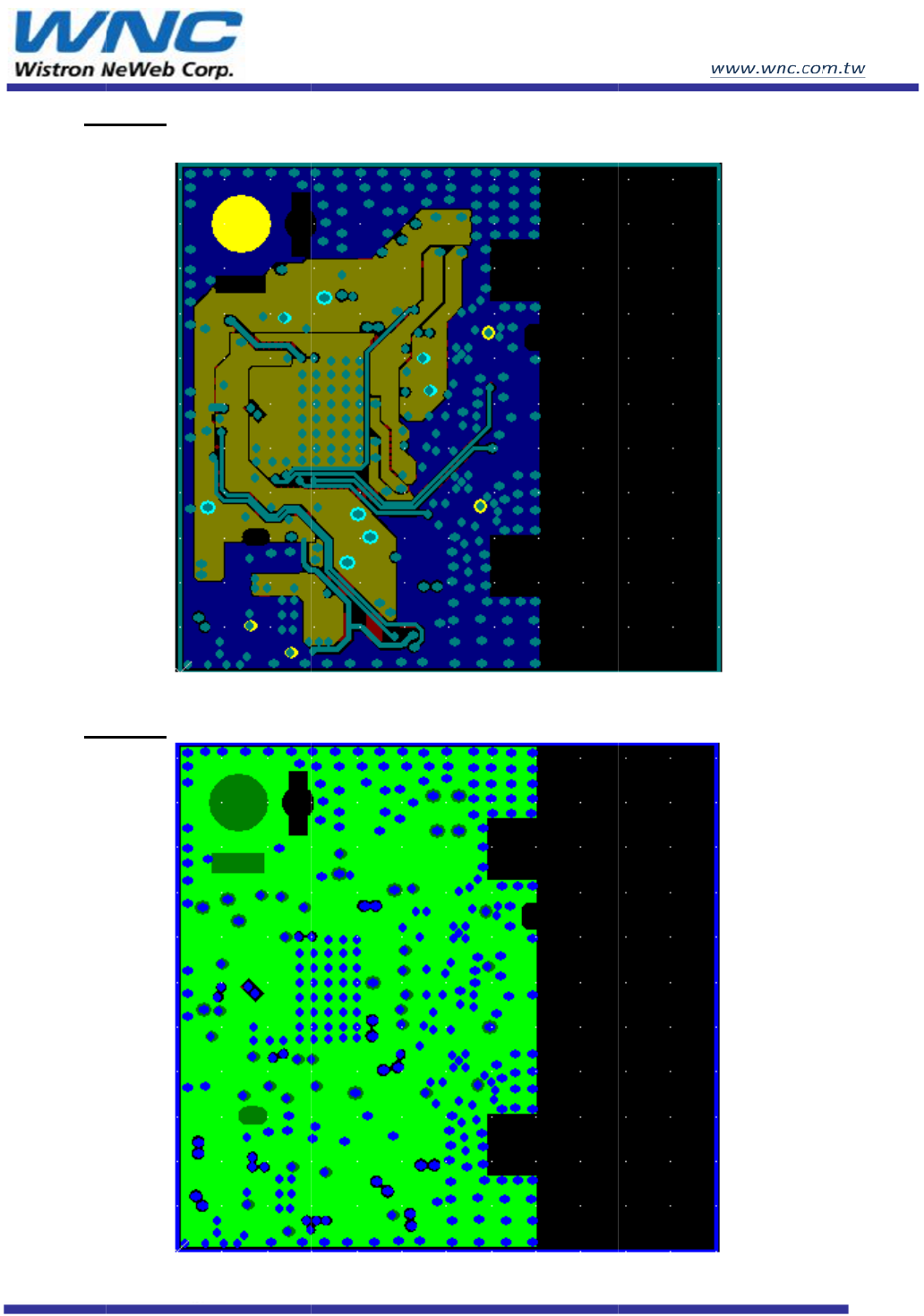
DNUB-S2
L
a
L
a
ay
er 1
ay
er 2
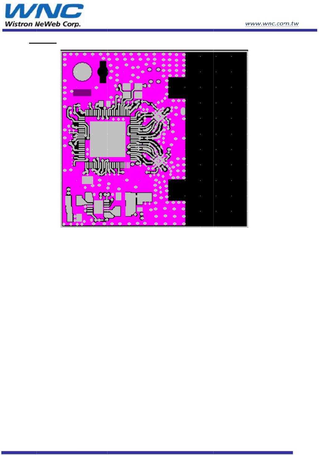
DNUB-S2
B
o
o
ttom
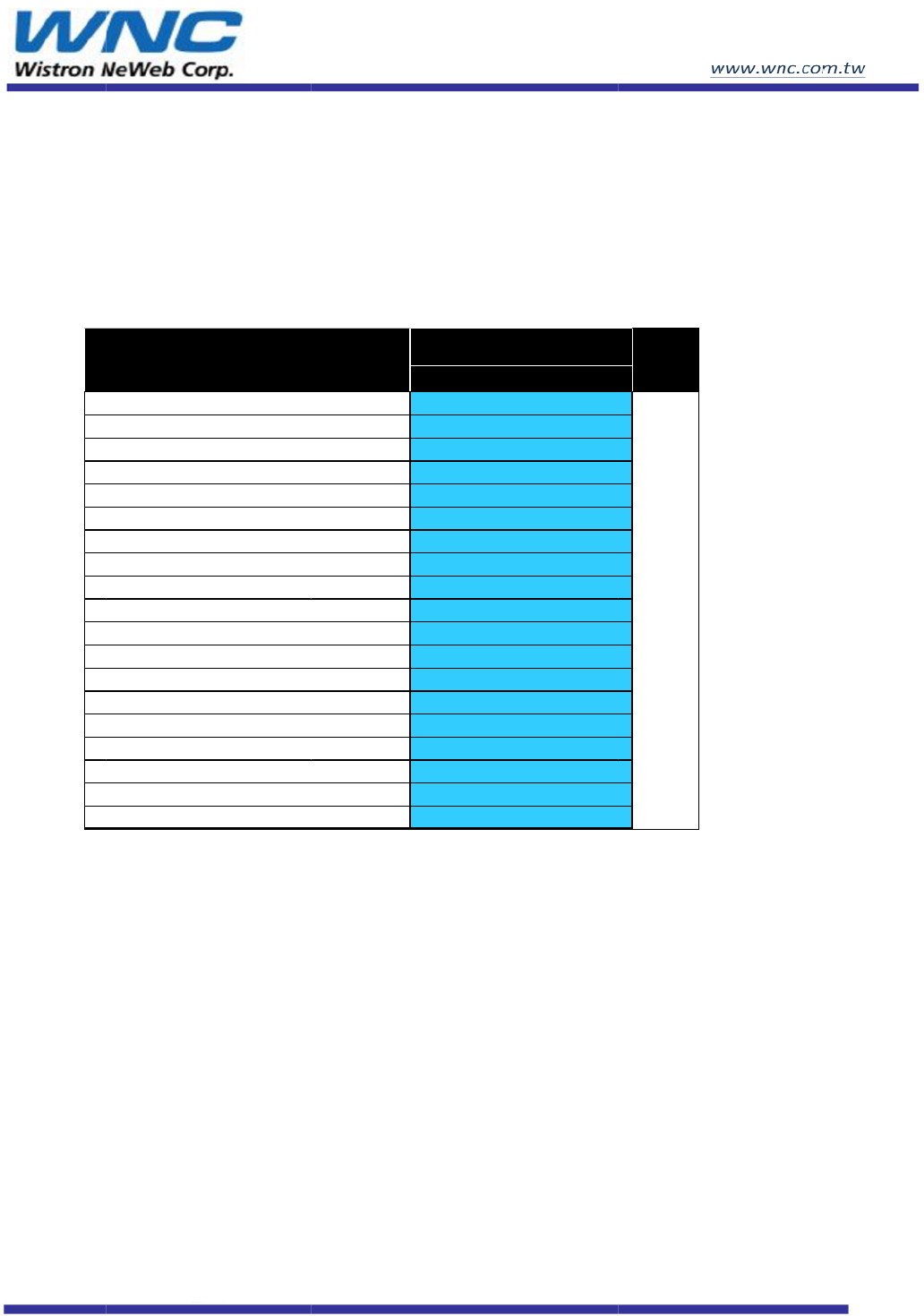
6
DNUB-S2
6
. Specif
i
6.1 S
u
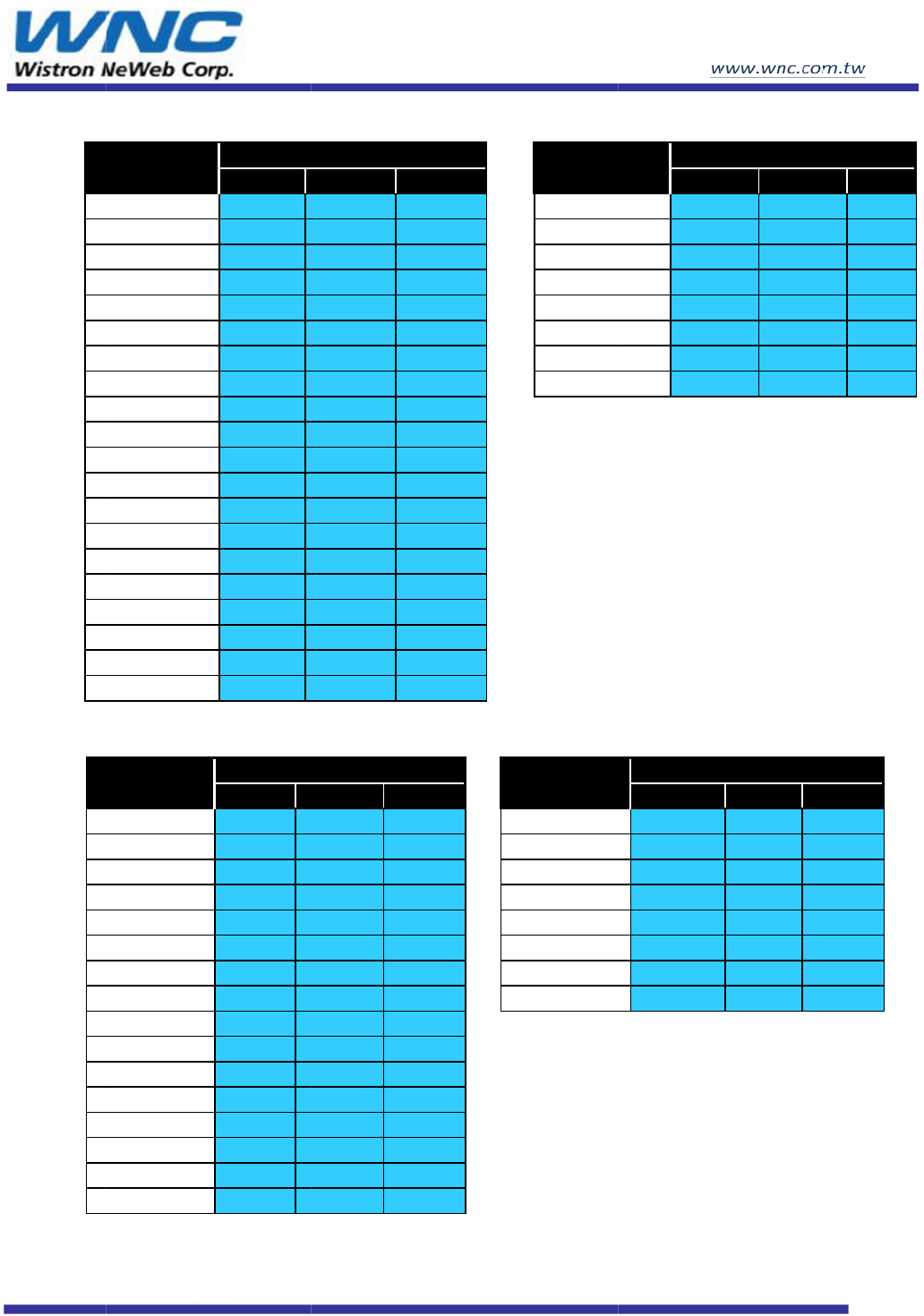
5
V
6.2 C
u
11
n
11
n
11
n
11
n
11
n
11
n
11
n
St
a
11
a
11
g
Ra
11
b
11
n
11
n
11
n
11
g
11
a
11
n
11
n
6.3 R
F
i
cations
:
u
ppl
y
Vol
t
V
±5% DC
u
rrent Co
n
g Cont. Tx@
H
n
g Cont. Tx@
H
n
g Cont. Tx@
H
n
g Cont. Tx@
H
n
a Cont. Tx@
H
n
a Cont. Tx@
H
n
a Cont. Tx@
H
a
ndby
a
Cont. RX
g
Cont. RX
dio off
C
b
Cont. Tx
n
a Cont. Tx@
H
n
a Cont. TX@
H
n
a Cont. TX@
H
g
Cont. Tx@ 6
M
a
Cont. Tx@ 6
M
n
g Cont. Tx@
H
n
g Cont. Tx@
H
F
power
a
g
e:
nsumttio
n
H
T20 MCS7
H
T40 MCS7
H
T20 MCS15
H
T40 MCS15
H
T20 MCS7
H
T40 MCS7
H
T20 MCS15
C
ondition
H
T40 MCS15
H
T20 MCS0
H
T40 MCS0
M
M
H
T20 MCS0
H
T40 MCS0
n
4
5
5V su
p
P
e
3
4
4
4
4
4
4
4
4
2
2
5
4
4
4
4
4
4
76
5
1
p
pl
y
onl
y
e
ak
3
30
4
92
4
67
4
87
4
70
4
86
4
87
4
56
4
45
2
10
2
10
5
1
4
72
4
93
4
85
4
63
4
88
Unit
mA
DNUB-S2
(T
y
(T
y
H
H
H
H
H
H
H
H
y
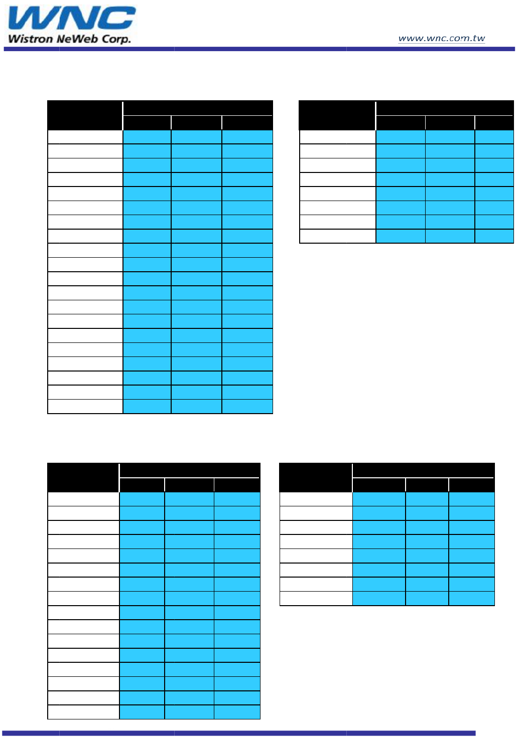
pical 2 Stre
a
1Mbps
2Mbps
5.5Mbps
11Mbps
6Mbps
9Mbps
12Mbps
18Mbps
24Mbps
36Mbps
48Mbps
54Mbps
HT20MCS0
HT20MCS1
HT20MCS2
HT20MCS3
HT20MCS4
HT20MCS5
HT20MCS6
HT20MCS7
20MHz BW
y
pical 2 Stre
a
6Mbps
9Mbps
12Mbps
18Mbps
24Mbps
36Mbps
48Mbps
54Mbps
H
T20MCS0/8
H
T20MCS1/9
H
T20MCS2/10
H
T20MCS3/11
H
T20MCS4/12
H
T20MCS5/13
H
T20MCS6/14
H
T20MCS7/15
20MHz BW
a
m power le
v
2412
19
19
19
19
18
18
18
18
18
18
18
18
18
18
18
18
18
18
18
18
a
m power le
v
5180
16
16
16
16
16
16
16
16
16
16
16
16
16
16
16
16
v
el: 2TX with
+
2437
19
19
19
19
18
18
18
18
18
18
18
18
18
18
18
18
18
18
18
18
MHz
v
el: 2TX with
5320
5
16
16
16
16
16
16
16
16
16
16
16
16
16
16
16
16
MHz
+
/- 2 dB toler
a
2472
19
19
19
19
18
18
18
18
18
18
18
18
18
18
18
18
18
18
18
18
+/- 2 dB tole
r
5
825
16
16
16
H
16
H
16
H
16
H
16
H
16
H
16
16
16
16
16
16
16
16
a
nce ) ( unit:
d
HT40M
C
HT40M
C
HT40M
C
HT40M
C
HT40M
C
HT40M
C
HT40M
C
HT40M
C
40MHz
r
ance ) ( unit:
d
HT40MCS0/8
HT40MCS1/9
H
T40MCS2/1
0
H
T40MCS3/11
H
T40MCS4/1
2
H
T40MCS5/1
3
H
T40MCS6/1
4
H
T40MCS7/1
5
40MHz BW
d
Bm )
24
2
C
S0 1
6
C
S1 1
6
C
S2 1
6
C
S3 1
6
C
S4 1
6
C
S5 1
6
C
S6 1
6
C
S7 1
6
BW
d
Bm )
MHz
5190
16
16
0
16
16
2
16
3
16
4
16
5
16
2
2 2437
6
16
6
16
6
16
6
16
6
16
6
16
6
16
6
16
`
MHz
5510
16
16
16
16
16
16
16
16
2462
16
16
16
16
16
16
16
16
5795
16
16
16
16
16
16
16
16
DNUB-S2
6.4
R
(T
y
H
H
H
H
H
H
H
H
(T
y
H
H
H
T
H
T
H
T
H
T
H
T
H
T
R
F Sensiti
v
y
pical 1 strea
1Mbps
2Mbps
5.5Mbps
11Mbps
6Mbps
9Mbps
12Mbps
18Mbps
24Mbps
36Mbps
48Mbps
54Mbps
H
T20 MCS0/8
H
T20 MCS1/9
H
T20 MCS2/10
H
T20 MCS3/11
H
T20 MCS4/12
H
T20 MCS5/13
H
T20 MCS6/1
4
H
T20 MCS7/1
5
20MHz BW
y
pical 1 strea
6Mbps
9Mbps
12Mbps
18Mbps
24Mbps
36Mbps
48Mbps
54Mbps
H
T20 MCS0/8
H
T20 MCS1/9
T
20 MCS2/10
T
20 MCS3/11
T
20 MCS4/12
T
20 MCS5/13
T
20 MCS6/14
T
20 MCS7/15
20MHz BW
v
it
y
m sensitivity
2412
-94
-92
-91
-86
-91
-91
-90
-88
-84
-81
-78
-75
-91
-89
-87
-83
-80
-76
4
-74
5
-72
m sensitivity
5180
-91
-90
-89
-87
-84
-81
-75
-73
-90
-88
-85
-81
-78
-75
-73
-71
level, 1RX w
i
2442
-94
-92
-91
-86
-91
-91
-90
-88
-85
-81
-78
-75
-92
-90
-87
-83
-80
-76
-74
-72
MHz
level, 1RX w
i
5320
5
-91
-
-90
-
-89
-
-87
-
-84
-
-81
-
-75
-
-73
-
-90
-
-88
-
-85
-
-81
-
-78
-
-75
-
-73
-
-71
-
MHz
i
th +4/- 2 dB
t
2472
-94
-92
-91
-86
-91
-91
-90
-88
-84
-81
-78
-75
-91
-89
-86
-82
-80
-76
-74
-72
i
th +4/- 2 dB
t
5
805
-
91
H
-
90
H
-
89
H
-
87
H
-
84
H
-
81
H
-
75
H
-
73
H
-
90
-
88
-
85
-
81
-
78
-
75
-
73
-
71
t
olerance) ( u
HT40 M
C
HT40 M
C
HT40 MC
S
HT40 MC
S
HT40 MC
S
HT40 MC
S
HT40 MC
S
HT40 MC
S
40MHz
t
olerance) ( u
H
T40 MCS0/8
H
T40 MCS1/9
H
T40 MCS2/1
0
H
T40 MCS3/1
1
H
T40 MCS4/1
2
H
T40 MCS5/1
3
H
T40 MCS6/1
4
H
T40 MCS7/1
5
40MHz BW
nit:dBm )
24
2
C
S0/8 -8
7
C
S1/9 -8
5
S
2/10 -8
3
S
3/11 -8
0
S
4/12 -7
7
S
5/13 -7
2
S
6/14 -7
1
S
7/15 -6
9
BW
nit:dBm )
MHz
5190
-88
-85
0
-83
1
-79
2
-76
3
-73
4
-70
5
-68
2
2 2437
7
-88
5
-85
3
-83
0
-80
7
-77
2
-72
1
-71
9
-69
MHz
5510
-88
-85
-83
-79
-76
-73
-70
-68
2462
-87
-85
-82
-80
-76
-72
-71
-69
5795
-88
-85
-83
-79
-76
-73
-70
-68
DNUB-S2
6.5 Environmental Spec.
Operating Temperature Range: 0degree C~ 60degree C
Storage Temperature Range: Temperature: -20~80℃ Humidity: 95%(MAX)
Operating Humidity Range: 10%~90% (No dew condensation)
7. MFG test items
7.1 Test Environmental
7.2 Test Items
TX:
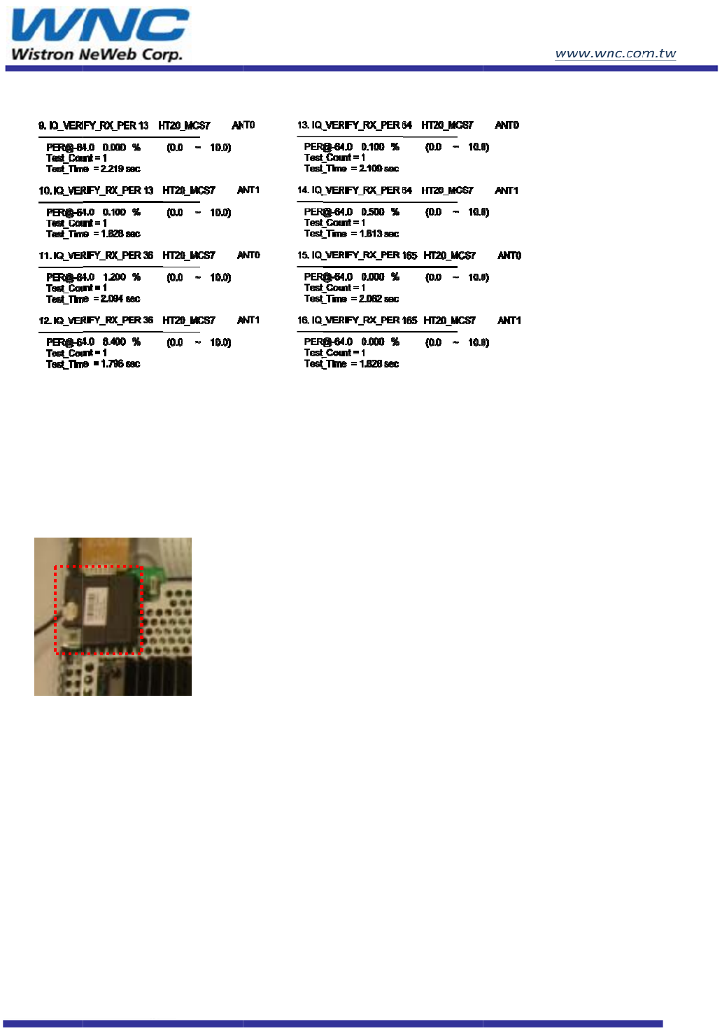
8
DNUB-S2
R
X
8
. Install
a
1. Be s
u
2. Inser
t
X
a
tion Pr
o
u
re to use the
t
the WIDT1
0
o
cedure
proper antis
0
B into the
m
tatic handlin
m
achine and
f
g technique
s
f
ix it by scre
s
.
w.

9
F
F
T
p
a
r
c
w
t
e
●
●
●
●
F
f
T
c
i
F
o
T
a
T
e
DNUB-S2
9
. Notice
F
CC State
m
F
ederal Co
m
T
his equip
m
p
ursuant to
a
gainst har
m
r
adiate radi
o
c
ause harm
f
w
ill not occ
u
elevision r
e
e
ncouraged
●
Reorient
●
Increase
●
Connect
t
connec
●
Consult t
h
F
CC Cautio
f
or complia
n
T
his devic
e
c
onditions:
(
nterference
F
or product
o
ther chann
T
his device
a
ntenna or
t
T
his device
e
nvironmen
t
m
ent
m
municati
o
m
ent has be
e
Part 15 of t
m
ful interfe
r
o
frequenc
y
f
ul interfere
u
r in a parti
c
e
ception, w
h
to try to co
or relocate
the separa
t
t
he equipm
e
ted.
h
e dealer o
r
n: Any cha
n
n
ce could v
o
e
complies
(
1) This de
v
received, i
n
available i
n
els is not p
o
and its a
n
t
ransmitter.
is going t
t
only.
o
n Commi
s
e
n tested a
n
he FCC Ru
r
ence in a r
e
y
energy an
d
nce to radi
o
c
ular install
a
h
ich can be
rrect the in
t
the receivi
n
t
ion betwee
n
e
nt into an
o
r
an experi
e
n
ges or mo
d
o
id the use
r
with Part
1
v
ice may n
o
n
cluding int
n
the USA/
C
o
ssible.
n
tenna(s) m
o be oper
a
s
sion Inter
f
n
d found to
les. These
l
e
sidential in
d
, if not inst
a
o
communic
a
tion. If this
determined
t
erference
b
n
g antenna.
n
the equip
m
o
utlet on a
c
e
nced radio
/
d
ifications n
’s authority
1
5 of the
F
o
t cause ha
erference t
h
C
anada ma
r
ust not be
a
ted in 5.1
5
f
erence St
a
comply wit
h
l
imits are d
e
stallation.
T
a
lled and u
s
ations. Ho
w
equipment
by turning
b
y one of th
e
m
ent and r
e
c
ircuit differ
/
TV technic
i
ot expressl
y
to operate
t
F
CC Rules.
rmful interf
e
h
at may ca
u
r
ket, only c
h
co-located
5
~5.25GHz
a
tement
h
the limits
f
e
signed to
p
T
his equipm
s
ed in acco
r
w
ever, there
does caus
e
the equipm
e
following
m
e
ceiver.
ent from th
a
i
an for help
.
y
approved
t
his equip
m
Operation
e
rence, an
d
u
se undesir
e
h
annel 1~11
or operati
o
frequency
f
or a Class
p
rovide rea
s
ent genera
t
r
dance with
is no guar
a
e
harmful in
t
ent off and
m
easures:
a
t to which
t
.
by the part
y
m
ent.
is subject
d
(2) this de
e
d operatio
can be op
e
o
n in conju
n
range, it i
s
B digital de
s
onable p
r
o
t
t
es, uses a
n
the instruc
t
a
ntee that in
t
erference
t
on, the use
t
he receive
r
y
responsi
b
to the foll
o
vice must
a
n.
e
rated. Sel
e
n
ction with
s
restricted
vice,
t
ection
n
d can
t
ions, may
terference
t
o radio or
r is
r
is
b
le
o
wing two
a
ccept any
e
ction of
any other
in indoor

I
F
T
T
y
I
T
c
2
h
f
A
a
U
I
s
i
s
a
t
a
t
m
L
T
A
s
O
a
u
DNUB-S2
MPORTAN
F
CC Radia
t
T
his equip
m
T
his equip
m
y
our body.
MPORTA
N
T
his modul
e
c
ompliance
2
0cm mini
m
h
ost this m
o
f
orth for an
p
A
ny change
a
uthority to
U
SERS M
A
n the users
s
eparation
w
nformed th
a
s
atisfied. T
h
a
pproved b
y
he end pro
d
a
vailable in
he followin
g
m
ust accep
t
L
ABEL OF
T
he final en
A
3LWIDT1
0
s
tatement h
O
peration i
s
a
nd (2) this
u
ndesired o
T NOTE:
t
ion Expos
m
ent compli
e
m
ent should
N
T NOTE:
e
is intende
d
requireme
n
m
um distan
c
o
dule is inte
g
p
opulation/
u
s or modifi
c
operate thi
s
A
NUAL OF
T
manual of
t
w
ith the ant
e
a
t the FCC
r
h
e end user
y
the manu
f
d
uct is sma
l
the users
m
g
two condi
t
t
any interf
e
THE END
P
d product
m
0
B ". If the s
as to also
b
s
subject to
t
device mu
s
peration.
ure State
m
e
s with FC
C
be installe
d
d
for OEM i
n
n
t of the en
d
e has to be
g
rated into.
u
ncontrolle
d
c
ations not
e
s
equipmen
t
T
HE END
P
t
he end pro
e
nna while
t
r
adio-frequ
e
has to als
o
f
acturer cou
l
ler than 8x
1
m
anual: Thi
s
t
ions: (1) th
i
e
rence rece
i
P
RODUCT:
m
ust be lab
e
ize of the e
n
b
e available
t
he followin
g
s
t accept an
m
ent:
C
radiation
e
d
and opera
t
n
tegrator.
T
d
product,
w
able to be
Under suc
h
d
environm
e
e
xpressly a
p
t
.
P
RODUCT:
duct, the e
n
t
his end pr
o
e
ncy expos
u
o
be inform
e
ld void the
u
1
0cm, then
s
device co
m
i
s device m
a
i
ved, includ
i
e
led in a vis
n
d product i
s
on the lab
e
g
two condi
t
y interfere
n
e
xposure li
m
t
ed with mi
n
T
he OEM in
t
w
hich integr
a
maintained
h
configura
t
e
nt can be
s
p
proved by
n
d user has
o
duct is inst
a
u
re guidelin
e
d that any
c
u
ser's auth
o
additional
F
m
plies with
P
a
y not cau
s
i
ng interfer
e
ible area wi
s
larger tha
n
e
l: This de
v
t
ions: (1) thi
n
ce receive
d
m
its set forth
n
imum dista
t
egrator is
s
a
tes this m
o
between t
h
t
ion, the FC
s
atisfied.
the manuf
a
to be infor
m
a
lled and o
p
es for an u
n
c
hanges or
o
rity to ope
r
F
CC part 1
5
P
art 15 of
F
s
e harmful i
n
e
nce that m
a
th the follo
w
n
8x10cm,
t
v
ice compli
e
s device m
a
d
, including
for an unc
o
nce 20cm
b
s
till respons
i
o
dule.
h
e antenna
a
C radiation
a
cture
r
coul
d
m
ed to kee
p
p
erated. Th
n
controlled
modificatio
n
r
ate this eq
u
5
.19 statem
e
F
CC rules.
O
n
terference
a
y cause u
n
w
ing " Cont
a
t
hen the foll
o
e
s with Part
a
y not caus
e
interferenc
e
o
ntrolled en
v
b
etween the
i
ble fo
r
the
F
a
nd the us
e
exposure li
d
void the
u
p
at least 2
0
e end user
environme
n
n
s not expr
e
u
ipment. If t
e
nt is requi
r
O
peration is
and (2) thi
s
n
desired op
a
ins TX FC
C
o
wing FCC
15 of FCC
r
e
harmful in
e
that may
c
v
ironment.
radiator &
F
CC
e
rs for the
mits set
u
ser's
0
cm
has to be
n
t can be
e
ssly
he size of
r
ed to be
subject to
s
device
eration.
C
ID:
part 15.19
r
ules.
terference
c
ause

I
T
O
t
t
C
F
o
T
a
T
o
i
T
i
T
t
T
e
s
H
5
L
DNUB-S2
C Stateme
n
T
his Class
B
O
peration i
s
his device
m
he device.
C
et apparei
l
F
or product
o
ther chann
T
his device
a
ntenna or
t
T
he device
c
o
r operatio
n
nformation
T
he device
f
nterference
T
he maxim
u
o comply
w
T
he maxim
u
e
.i.r.p. limit
s
s
ection A9.
2
H
igh-power
5
250-5350
M
L
E-LAN de
v
n
t
B
digital ap
p
s
subject to
t
m
ust accep
t
l
numériqu
e
available i
n
els is not p
o
and its ant
e
t
ransmitter.
c
ould auto
m
n
al failure.
N
or the use
o
f
or the ban
d
to co-chan
u
m antenna
w
ith the e.i.r.
u
m antenna
s
specified f
o
2
(3).
radars are
M
Hz and 5
6
v
ices.
p
aratus co
m
t
he followin
g
t
any interfe
r
e
de la clas
s
n
the USA/
C
o
ssible.
e
nna(s) mu
s
m
atically dis
c
N
ote that thi
s
o
f repetitive
d
5150-525
0
nel mobile
s
gain permi
t
p. limit.
gain permi
o
r point-to-
p
allocated a
s
6
50-5850 M
m
plies with
C
g
two condi
t
r
ence, inclu
s
e B est co
n
C
anada ma
r
s
t not be co
c
ontinue tr
a
s
is not inte
codes whe
0
MHz is o
n
s
atellite sy
s
t
ted (for de
v
tted (for de
v
p
oint and n
o
s
primary u
s
Hz and the
s
C
anadian I
C
t
ions: (1) thi
ding interfe
n
forme á la
r
ket, only c
h
-located or
a
nsmission i
nded to pr
o
re required
n
ly for indo
o
s
tems.
v
ices in the
b
v
ices in the
o
n point-to-
p
s
ers (mean
i
s
e radars c
o
C
ES-003.
s device m
a
rence that
m
norme NM
B
h
annel 1~11
operation i
n
n case of a
b
o
hibit trans
m
by the tec
h
o
r usage to
r
b
ands 525
0
band 5725
-
p
oint opera
t
i
ng they ha
v
o
uld cause
a
y not caus
e
m
ay cause
u
B
-003 du C
a
can be op
e
n
conjuncti
o
b
sence of i
n
m
ission of c
o
h
nology.
r
educe pot
e
0
-5350 MHz
-
5825 MHz
)
t
ion as app
r
v
e priority)
o
interferenc
e
e
interferen
c
u
ndesired o
p
a
nada.
e
rated. Sel
e
o
n with any
o
n
formation t
o
o
ntrol or sig
e
ntial for ha
r
and 5470-
5
)
to comply
r
opriate, as
o
f the band
s
e
and/or da
m
c
e, and (2)
p
eration of
e
ction of
o
ther
o
transmit,
naling
r
mful
5
725 MHz)
with the
stated in
s
m
age to

I
I
T
e
t
I
T
c
2
h
s
A
a
U
I
s
i
s
a
i
s
I
i
c
L
T
6
DNUB-S2
MPORTAN
C Radiatio
T
his equip
m
e
nvironmen
t
he radiator
MPORTA
N
T
his modul
e
c
ompliance
2
0cm mini
m
h
ost this m
o
s
et forth for
A
ny change
a
uthority to
U
SERS M
A
n the users
s
eparation
w
nformed th
a
s
atisfied. T
h
a
pproved b
y
s
required t
o
CES-003.
O
nterference
c
ause unde
s
L
ABEL OF
T
he final en
6
49E-WIDT
T NOTE:
n Exposur
e
m
ent compli
e
t
. This equi
p
& your bod
y
N
T NOTE:
e
is intende
d
requireme
n
m
um distan
c
o
dule is inte
g
an populati
s or modifi
c
operate thi
s
A
NUAL OF
T
manual of
t
w
ith the ant
e
a
t the IC ra
d
h
e end user
y
the manu
f
o
be availa
b
O
peration i
s
and (2) thi
s
s
ired opera
t
THE END
P
d product
m
10B ".
e
Stateme
n
e
s with IC
R
p
ment sho
u
y
.
d
for OEM i
n
n
t of the en
d
e has to be
g
rated into.
on/uncontr
o
c
ations not
e
s
equipmen
t
T
HE END
P
t
he end pro
e
nna while
t
d
io-frequen
c
has to als
o
f
acturer cou
b
le in the u
s
s
subject to
t
s
device mu
t
ion.
P
RODUCT:
m
ust be lab
e
n
t:
R
SS-102 ra
d
u
ld be instal
l
n
tegrator.
T
d
product,
w
able to be
Under suc
h
o
lled enviro
n
e
xpressly a
p
t
.
P
RODUCT:
duct, the e
n
t
his end pr
o
c
y exposur
e
o
be inform
e
ld void the
u
s
ers manual
t
he followin
g
st accept a
n
e
led in a vis
d
iation exp
o
l
ed and op
e
T
he OEM in
t
w
hich integr
a
maintained
h
configurati
n
ment can
b
p
proved by
n
d user has
o
duct is inst
a
e
guideline
s
e
d that any
c
u
ser's auth
o
: This Clas
s
g
two condi
n
y interfere
n
ible area wi
o
sure limits
s
e
rated with
m
t
egrator is
s
a
tes this m
o
between t
h
on, the IC
R
b
e satisfied
the manuf
a
to be infor
m
a
lled and o
p
s
for an unc
o
c
hanges or
o
rity to ope
r
s
B digital a
p
tions: (1) t
h
n
ce receive
d
th the follo
w
s
et forth fo
r
m
inimum di
s
s
till respons
i
o
dule.
h
e antenna
a
R
SS-102 ra
d
.
a
cture
r
coul
d
m
ed to kee
p
p
erated. Th
o
ntrolled en
modificatio
n
r
ate this eq
u
p
paratus c
o
h
is device
m
d
, including
w
ing " Cont
a
r
an uncont
r
s
tance 20c
m
i
ble fo
r
the
I
a
nd the us
e
d
iation exp
o
d
void the
u
p
at least 2
0
e end user
vironment
c
n
s not expr
e
u
ipment. IC
o
mplies with
m
ay not cau
s
interferenc
a
ins TX IC :
r
olled
m
between
I
C
e
rs for the
o
sure limits
u
ser's
0
cm
has to be
c
an be
e
ssly
statement
Canadian
s
e harmful
e that may