Samsung SGH D500 Service Manual User To The 390cbeb6 14aa 4835 B813 45aa78084d58
User Manual: Samsung SGH-D500 to the manual
Open the PDF directly: View PDF ![]() .
.
Page Count: 52

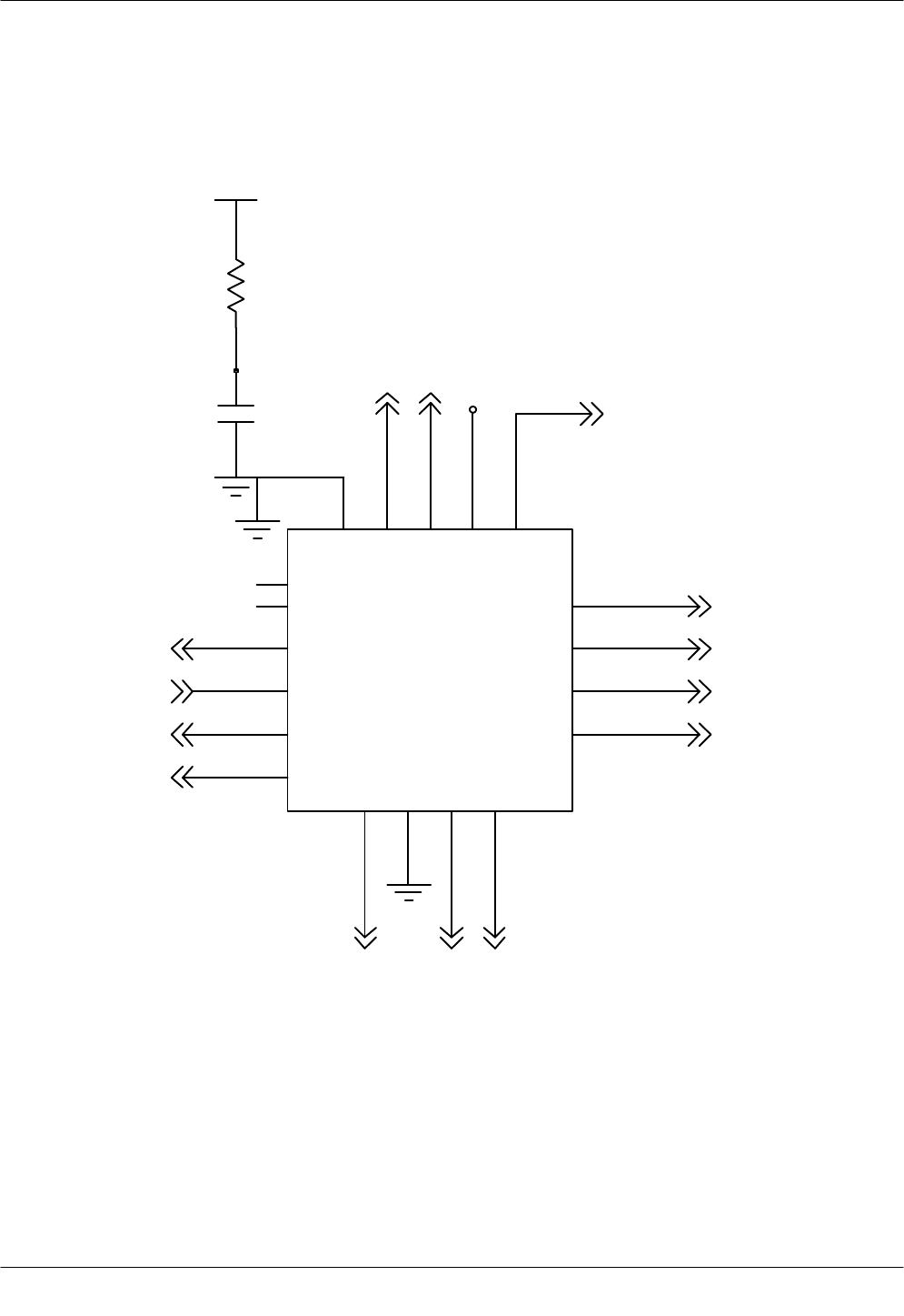
GPRS TELEPHONE
SGH-D500
GPRS TELEPHONE CONTENTS
1. Specification
2. Circuit Description
3. Exploded Views and Parts List
4. Electrical Parts List
5. Block Diagrams
6. PCB Diagrams
7. Flow Chart of Troubleshooting

Samsung Electronics Co.,Ltd. Nov. 2004
Printed in South Korea.
Code No.: GH68-05955A
BASIC.
ⓒ
This Service Manual is a property of Samsung Electronics Co.,Ltd.
Any unauthorized use of Manual can be punished under applicable
International and/or domestic law.
SAMSUNG Proprietary-Contents may change without notice
1. SGH-D500 Specification
ThisDocumentcan notbe used withoutSamsung'sauthorization
1-1
PCS1900
1850~1910
1930~1990
512~810
80MHz
270.833kbps
3.692us
576.9us
4.615ms
0.3GMSK
30dBm~0dBm
0pcl~15pcl
-100dBm
8
-
1. GSMGeneralSpecification
GSM900
Phase1
EGSM900
Phase2
DCS1800
Phase1
Freq.Band[MHz]
Uplink/Downlink
890~915
935~960
880~915
925~960
1710~1785
1805~1880
ARFCNrange1~124 0~124 &
975~1023 512~885
Tx/Rxspacing 45MHz45MHz95MHz
Mod.Bit rate
/Bit Period
270.833kbps
3.692us
270.833kbps
3.692us
270.833kbps
3.692us
TimeSlotPeriod
/FramePeriod
576.9us
4.615ms
576.9us
4.615ms
576.9us
4.615ms
Modulation 0.3GMSK0.3GMSK0.3GMSK
MS Power33dBm~5dBm33dBm~5dBm30dBm~0dBm
PowerClass 5pcl~19pcl5pcl~19pcl0pcl~15pcl
Sensitivity-102dBm-102dBm-100dBm
TDMAMux 8 8 8
Cell Radius35Km35Km2Km
SAMSUNG Proprietary-Contents may change without notice
ThisDocumentcan notbe used withoutSamsung'sauthorization
Specification
1-2
TXPower
control levelPCS1900
0 30±3 dBm
1 28±3 dBm
2 26±3 dBm
3 24±3 dBm
4 22±3 dBm
5 20±3 dBm
6 18±3 dBm
7 16±3 dBm
8 14±3 dBm
9 12±4 dBm
10 10±4 dBm
11 8±4dBm
12 6±4 dBm
13 4±4 dBm
14 2±5 dBm
15 0±5 dBm
2. GSMTXpower class
TXPower
control levelDCS1800
0 30±3 dBm
1 28±3 dBm
2 26±3 dBm
3 24±3 dBm
4 22±3 dBm
5 20±3 dBm
6 18±3 dBm
7 16±3 dBm
8 14±3 dBm
9 12±4 dBm
10 10±4 dBm
11 8±4dBm
12 6±4 dBm
13 4±4 dBm
14 2±5 dBm
15 0±5 dBm
TXPower
control levelGSM900
5 33±3 dBm
6 31±3 dBm
7 29±3 dBm
8 27±3 dBm
9 25±3 dBm
10 23±3 dBm
11 21±3 dBm
12 19±3 dBm
13 17±3 dBm
14 15±3 dBm
15 13±3 dBm
16 11±5 dBm
17 9±5 dBm
18 7±5 dBm
19 5±5 dBm
SAMSUNG Proprietary-Contents may change without notice
2. SGH-D500 Circuit Description
ThisDocumentcan notbe used withoutSamsung'sauthorization
2-1
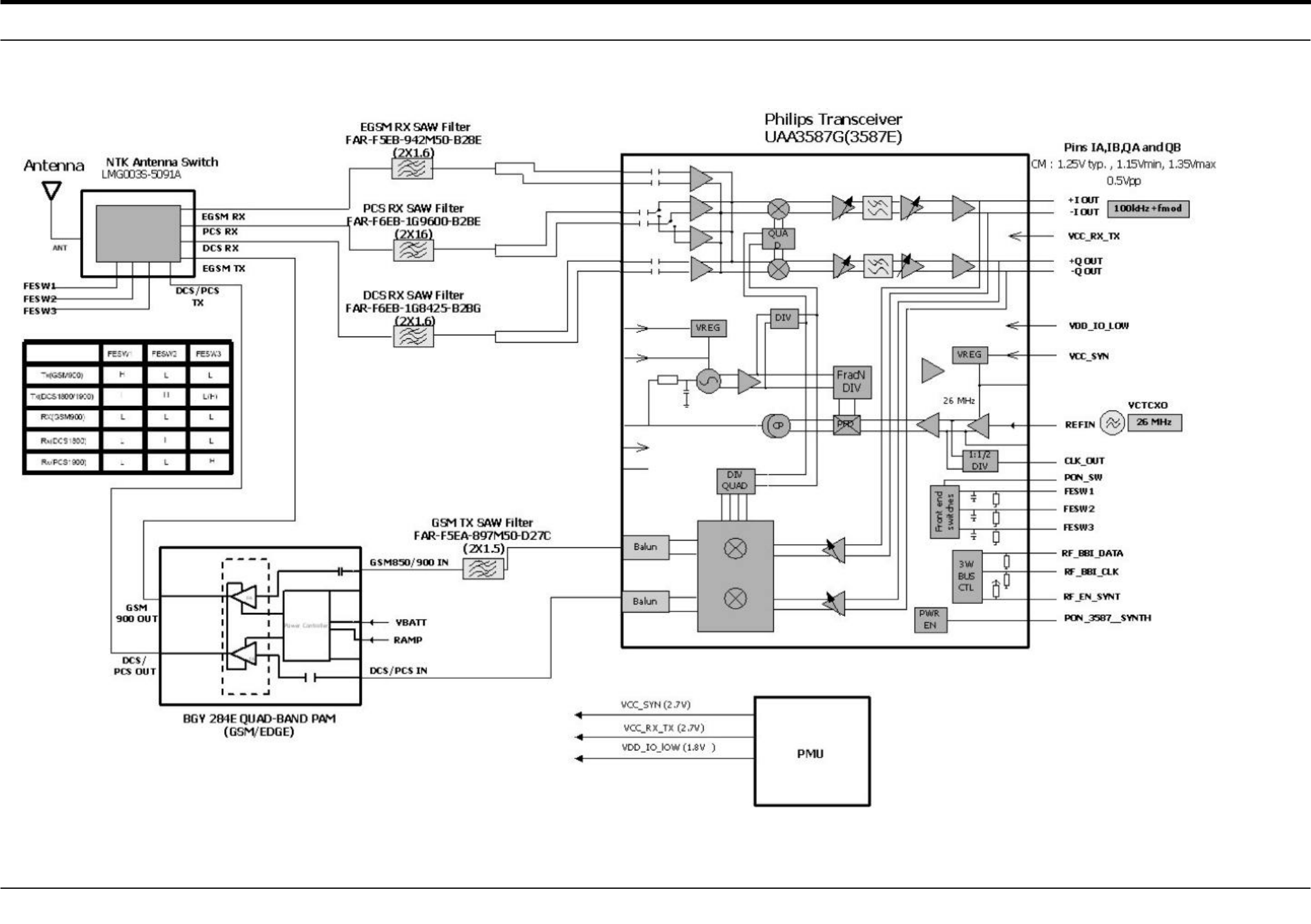
1. SGH-D500 RFCircuitDescription
1)RXPART
1.ANTENNA SWITCH(U100 SWICHPLEXER)
→Switching Tx,Rx pathforGSM900,DCS1800 and PCS1900 by logic controlling.
2.ANTENNA SWITCHControlLosic(U100)→TruthTable
VC1VC2VC3
TxMode(GSM900)LHL
TxMode(DCS1800/1900)L(H)LH
RxMode(GSM900)L L L
RxMode(DCS1800)L L L
RxMode(PCS1900)HL L
3.FILTER
ToconvertElectromagneticFieldWavetoAcousticWave and then pass thespecificfrequency band.
-GSMFILTER(F100)→For filtering thefrequency band between 925 and 960 MHz
-DCS FILTER(F102)→For filtering thefrequency band between 1805 and 1880 MHz.
-PCS FILTER(F101)→For filtering thefrequency band between 1930 and 1990 MHz.
4.VC-TCXO (U101)
Thismodulegeneratesthe26MHzreference clockto drivethelogic and RF.
It isturnedonwhenthesupply voltageVcc(SYN)isapplied.
Afterbuffering areference clock of26MHzis suppliedtotheotherpartsofthesystem
through thetransceiverpinCLKOUT.
5.TRANSCEIVER(U102)
ThischipisfullyintegratedGSMGPRSquad-band transceiverwithtransmit baluns,loop filtersand mostofthe
passive component init.
And alsofullyintegratedfractionalNRFsynthesizerwithAFCcontrolpossibility,RFVCO withintegratedsupply
regulator.Semi integratedreference oscillatorwithintegratedsupplyregulator.
RFReceiver front-end amplifiestheE-GSM900,DCS1800 and PCS1900 aerialsignal,convert the chosenchannel
downtoalowIFof100kHz.
InIFsection,furtheramplifiesthewantedchanneloutput level tothedesired value and rejectsDC.
2)TXPART
Thetransmitterisfully differentialusing adirectup conversion architecture.Itconsistsofasignalsideband
powerup mixer.Gainiscontrolled by 6 dBvia3-wireserialbusprograming.ThefullyintegratedVCOand power
mixerachieveLOsuppression,quadraturephase error,quadrature amplitudebalance and lownoisefloorspecification.
Outputmatching/balun componentsdrive a standard 50 ohms single endedload.

SAMSUNG Proprietary-Contents may change without notice
ThisDocumentcan notbe used withoutSamsung'sauthorization
CircuitDescription
2-2
2. Baseband CircuitdescriptionofSGH-D500
1.PCF50603 (U400)
1.1.PowerManagement
Eight low-dropoutregulatorsdesignedspecificallyforGSMapplicationspowertheterminaland helpensureoptimal
systemperformance and long batterylife.Aprogrammableboostconverterprovides supportfor1.8V,3.0VSIMs,
whileaself-resetting,electronicallyfusedswitchsuppliespowertoexternalaccessories.Ancillarysupportfunctions,
suchasRTCmodule and High VoltageChargepump,Clock generator,aidinreducing both boardarea and system
complexity.
I2C BUSserial interface providesaccess tocontroland configuration registers.Thisinterface givesamicroprocessor
full controlofthePCF50603 and enables systemdesignerstomaximize bothstandby and talktimes.
Supervisoryfunctions.including aresetgenerator,aninputvoltagemonitor,and atemperaturesensor,supportreliable
systemdesign.Thesefunctionsworktogethertoensurepropersystembehaviorduring start-up orinthe eventofa
fault condition(lowmicroprocessorvoltage,insufficientbatteryenergy,orexcessivedietemperature).
1.2.BacklightBrightness Modulator
TheBacklightBrightness Modulator (BBM)containsaprogrammablePulse-widthmodulator (PWM)and FET to
modulatetheintensity ofaseriesofLED’sortocontrolaDC/DCconverterthatdrivesLCDbacklight.
Thisphone(SGH-D500)usePWMcontrol tocontrast thebacklightbrightness.
1.3.ClockGenerator
TheClockGenerator (CG)generatesall clocksforinternaland externalusage.The32.768 kHz crystaloscillator
providesanaccuratelowclockfrequencyforthePCF50603 and othercircuitry.
2.LCDConnector
LCDisconsisted ofmainLCD(color26KTFT LCD).
ChipselectsignalsintheU305,LCD_CS,canenableLCD.BACKLIGHTsignalenableswhiteLEDofmainLCD.These
signal isfromU400.
16-bit datalines(LD(0)~LD(15)) transfersdata and commandstoLCD.Data and commandsuse"RS"signal.If this signal
ishigh,InputstoLCDare commands.If it islow,InputstoLCDaredata.Thesignalwhichinformstheinputoroutput
statetoLCD,isrequired.But this systemisnotnecessarythis signal.So"L_WR"signal isusedtowritedataor
commandstoLCD.PowersignalsforLCDare"VDD_IO_HIGH".
3.IRDA
This systemusesIRDA module,HSDL_3209,Agilent's.Thishas signals,"IRDA_EN"(enablesignal),"IRDA_RXD"(input
data)and "IRDA_TXD"(outputdata).Thesesignalsare connectedtoPCF5213EL1through BTModule.

SAMSUNG Proprietary-Contents may change without notice
CircuitDescription
ThisDocumentcan notbe used withoutSamsung'sauthorization
2-3
4.Key
Thisisconsisted ofkeyinterface pinsKEY_ROW(0:4)and KEY_COL(0:4)inPCF5213EL1.Thesesignalscomposethe
matrix.Result ofmatrixinformsthekeystatusto keyinterface inthePCF5213EL1.Poweron/off keyis seperatedfrom
thematrix.So poweron/off signal isconnectedwithPCF50603 toenablePCF50603.KeyLEDisconsisted ofsixwhite
LEDsforsub keyand twelvewhiteLEDsformain key.WhiteLEDforsub key usetheVBATvoltage.
"SLIDER_KEY_ON"signalenablesTransistor forsub key backlight.
Main keyLEDusethe3.3VLDO forasupply voltage.KEY_LED_ON signalenableseightwhiteLED.
"FLIP"informsthestatusofslide(open orclosed)tothePCF5213EL1.Thisusesthehall effectIC,A3212ELH.
AmagnetunderLCDenablesA3212ELH.
5.EMIESDFilter
This systemusestheEMIESDfilter,U500 to protectnoisefromIFCONNECTORpart.
6.IFconnetor
It is18-pinconnector.Theyaredesignedto useVBAT,V_EXT_CHARGE,USB_D+,+VBUS,USB_D-,TXD1,RXD1,
AUX_ON,EXT1,EXT2,HFK_SPK,HFK_MICand GND.Theyconnectedto powersupplyIC,microprocessorand signal
processor IC.
7.BatteryChargeManagement
Acomplete constant-current/constant-voltagelinearcharger forsingle cell lithium-ion batteries.
If TAconnectedto phone,"V_EXT_CHARGE"enable charger ICand supplycurrent to battery.
Whenfault condition caused,"CHG_ON"signal levelchangelowto high and charger ICstop charging process.
8.Audio
HFR_Pand HFR_NfromPCF5213El1are connectedtothemainspeakervia analog switches.MIC_Pand MIC_N
are connectedtothemainMICaswell.EAR1isthesource ofExternalSpeaker.YMU765 isasynthesizerLSI for
mobilephones.ThisLSIhasabuilt-inspeakeramplifier foroutputting soundsthatareused by mobilephonesinaddition
to gamesoundsand ringing melodiesthatarereplayed by asynthesizer.
Thesynthesizersection adopts“stereophonichybridsynthesizersystem”thataregivenadvantagesofbothFM
synthesizersand WaveTablesynthesizerstoallowsimultaneousgeneration ofup to32FMvoicesand 32 Wave
Tablevoices.
Itprovides simultaneousgeneration ofup to64tonesby stereophonichybridsynthesizer.
YMU765 hasbuilt aspeakeramplifierofwhichmaximumout is580 mWatSPVDD=3.6Vinthisdevice.
ThereisStereophonic analog outputforHeadphone.
9.Memory
This systemusesSamsung'smemory,KBJ10KB00M.TheKBJ10KB00MisaMulti ChipPackageMemorywhich
combines256Mbit SynchronousBurstMulti Bank NORFlashMemoryand two 512Mbit OneNAND Flashand
128Mbit SynchronousBurstUtRAM.
Ithas16 bit dataline,HD[1~16]whichisconnectedtoPCF5213 and MV319,also has24 bit address lines,
HA[1~24].There are3chipselectsignals,CS0n_FLASH,CS4n_NAND,and CS1n_RAM.
IntheWrting process,WEnisfallentolowand it enableswriting process to operate.During reading process,
OEnisfallentolowand it enablesreading process to operate.EachchipselectsignalsinthePCF5213 choose
differentmemories.

SAMSUNG Proprietary-Contents may change without notice
ThisDocumentcan notbe used withoutSamsung'sauthorization
CircuitDescription
2-4
10.PCF5213EL1
ThePCF5213EL1ismainlycomposed ofembededDSP and ARMcore.TheDSP subsystemincludestheSaturn
DSP corewithembeddedRAMand ROM,and asetofperipherals.Ithas24kx16 bitsPRAM,104k*16 bits,
32k*16 XYRAMand 63k*16 XYROMintheDSP.
TheARM946E-SconsistsofanARM9E-Sprocessorcore,8 kbyteinstruction cache and 8 kbytedata cache,
tghtly-coupledITCM(Instruction TightlyCoupledMemory)and DTCM(DataTightlyCoupledMemory)memories,a
memory protection unit,and anAMBA(AdvancedMicrocontrollerBusArchitecture)AHB(Advanced
High-performance Bus)businterface withawritebuffer.
HD(0:15),datalinesand HA(0:23),address linesare connectedtoKBJ10KB00M(memory),MV319DNQ (imagedsp)
and YMU765 (melody IC).Ithas64 kbyteSC RAM(0.5Mbit)and 32 kbyteSCprogramROMforbootstrap
loaderintheARMcore.
HD(0:15),datalinesand HA(0:23),address linesare connectedtomemoryand YMU765 tocommunicate.
MV319DNQ(CameraDSP Chip)controlsthe communication betweenARMcore and DSP core.
OEn,WEncontrol the access ofmemory.KROW,and KCOLrecognize thekeystring inputstatus.Thesystem
communicateswithIrDA viaIrDA_TXD,IrDA_RXD.
Ithas J-TAG controlpins(TDI/TDO/TCK) forARMand DSP core.J-SEL signalcontrolsdifferentaccess toARM
and DSP core.
ADC(Analog toDigitalConvertor) receivesthe condition oftemperature,batterytype and battery voltage.
11.TCO-5871U(26MHz)
This systemusesthe26MHzTCXO,TCO-5871U,Toyocom.AFCcontrolsignalformPCF5213 controls
frequencyfrom26MHzx-tal.Itgeneratesthe clockfrequency.ThisclockisconnectedtoPCF5213,YMU765 and
UAA3587.
12.CameraDSP(MV319DNQ)
MV319DNQ providesrich videofunctionsup to 30-framedisplaywithminimizedtasksinthehandsetmain processor
aswell ashardwarebasedreal-timeJPEGcompression and decompression.MV319DNQ directlytransmitsand
previewstheRGBdatatotheLCDgraphicmemory by processing thesensoroutputdata according tothe
handset'scommand.ItcansavetherawRGBdataup toVGA resoultion intoitsimagebufferand allowsthe
hostprocessorto downloadwithscalablesizedcompressed data.
Itutilizes16 bit databusforcommunication withthemain processor,including businterface types.
SAMSUNG Proprietary-Contents may change without notice
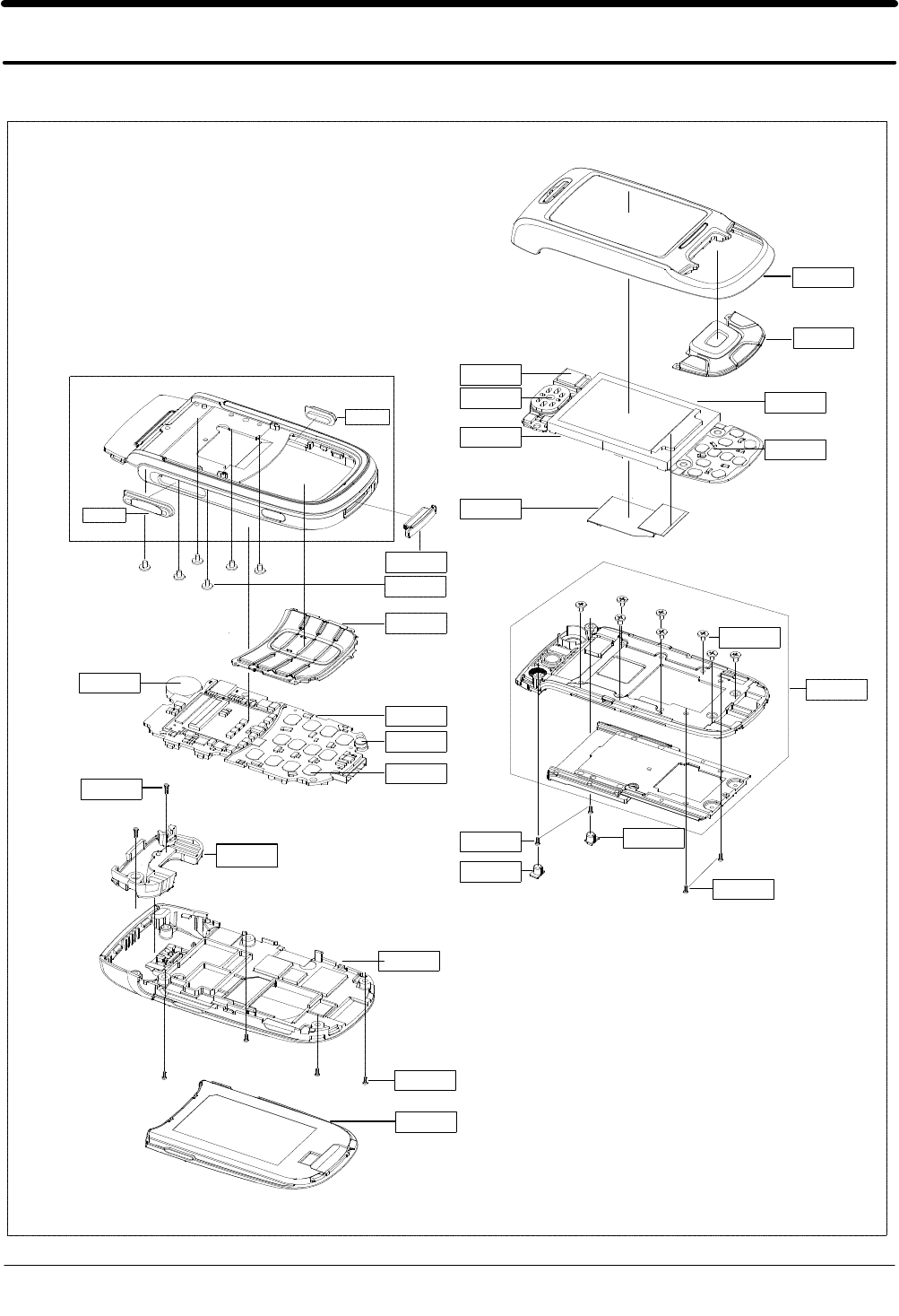
3. SGH-D500 ExplodedViewand its Partslist
3-1
ThisDocumentcan notbe used withoutSamsung'sauthorization
1.CellularphoneExplodedView-1
QCA01
QSP01
QMP02
QCR11
QMO01
QCR11
QSC16
QPC01
QKP02
QME02
QCR16
QLC01
QSC18
QCR16
QMP01
QRE01
QBA19
QCR11
QIF01
QMI01
QME01
QAN02
QFU01
QFL01
QCK01
QVO01
QCR08
QKP01
SAMSUNG Proprietary-Contents may change without notice
Explodedviewand its Partlist
3-2
ThisDocumentcan notbe used withoutSamsung'sauthorization
2.CellularphonePartslist
Location
NO.DescriptionSEC CODE Remark
QBA19 BATTERYGH43-01534D
QMP01 MAINPBAGH92-01852A
QMO01 MOTOR3101-001411
QMI01 MICROPHONEASSYGH30-00149A
QME01 UNITMETALDOMEGH59-01697A
QSP01 SPEAKER 3001-001636
QCR08 SCREW6001-001456
QCR11 SCREW6001-001654
QCR16 SCREW6001-001878
QLC01 LCDGH07-00611A
QPC01 PCB FPCB GH41-00700A
QCA01 UNITCAMERAGH59-01635A
QSC16 PMO-S/LSCREWCAP(L)GH72-17899A
QSC18 PMO-S/LSCREWCAP(R)GH72-17900A
QFU01 SLIDEUPPER GH75-05621A
QFR01 FONTCOVER GH75-05622A
QVO01 KEYVOLGH75-05626A
QCK01 CAMGH75-05627A
QFL01 SLIDELOWER GH75-05623A
QCR16 SCREW6001-001823
QKP01 KEYPADMAINGH75-05624A
QKP02 KEYPADSUBGH75-05625A
QMP02 SUBPBAGH92-01853A
QME02 UNITMETALDOMEGH59-01698A
QCR11 SCREW6001-001654
QAN02 INTENNAGH42-00479A
QRE01 REARCOVER GH75-05642A
QCR11 SCREW6001-001654
QIF01 IFCOVER GH72-17901A
SAMSUNG Proprietary-Contents may change without notice
Explodedviewand its Partlist
3-2
ThisDocumentcan notbe used withoutSamsung'sauthorization
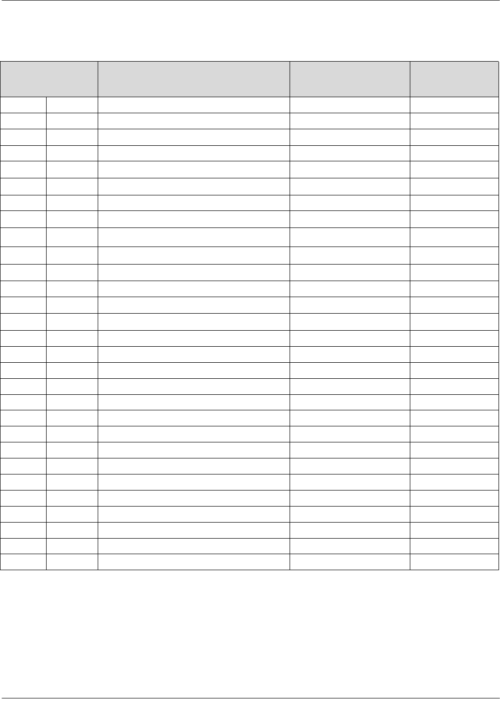
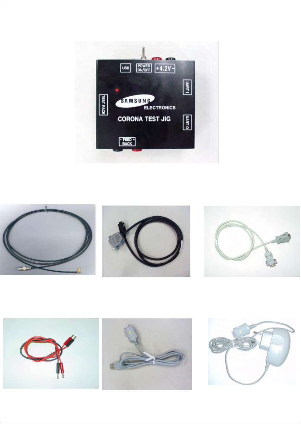
3.TestJig(GH80-01909A)
3-1.RFTestCable
(GH39-00283A)3-2.TestCable
(GH39-00337C)3-3.SerialCable
3-4.PowerSupplyCable3-5.DATACABLE
(GH39-00331A]3-6.TA
(GH44-00482A)
SAMSUNG Proprietary-Contents may change without notice
4. SGH-D500 ElectricalParts List
4-1
ThisDocumentcan notbe used withoutSamsung'sauthorization
MAIN
SEC CODEDesignLOC
0403-001387 ZD500
0403-001427 ZD501
0404-001172 D400
0404-001172 D401
0406-001104 ZD601
0406-001188 U500
0406-001190 ZD600
0407-001002 D600
0504-001113 Q500
0504-001113 Q505
0504-001113 Q506
0504-001151 U506
0505-001332 U306
0505-001518 Q200
0505-001938 U505
0601-001819 LED600
0601-001819 LED601
0601-001819 LED602
0601-001819 LED603
0601-001819 LED604
0601-001819 LED605
0601-001819 LED606
0601-001819 LED607
0601-001819 LED610
0601-001819 LED611
0604-001291 U301
0801-002237 U302
0801-002237 U308
0801-002294 U401
1001-001231 U601
1001-001231 U602
1001-001231 U604
1001-001231 U661
1001-001253 U662
1009-001010 U600
1109-001322 U307
1201-002213 PAM100
1202-001068 U663
1203-002837 U402
1203-003079 U403
1203-003079 U610
1203-003079 U665
1203-003568 U400
1203-003577 U503
1204-002138 U300
1205-002633 U102
1205-002636 U200
1404-001221 V500
1405-001082 TH600
1405-001082 TH601
1405-001082 V300
1405-001082 V301
1405-001082 V302
1405-001082 V303
1405-001082 V400
2007-000137 R510
2007-000138 R622
2007-000140 R602
2007-000140 R604
2007-000143 R210
2007-000143 R315
2007-000143 R316
2007-000147 R216
2007-000148 R101
2007-000148 R111
2007-000148 R201
2007-000148 R212
2007-000148 R300
2007-000148 R304
2007-000148 R312
2007-000148 R504
2007-000151 R314
2007-000152 C500
2007-000160 R515
2007-000162 R206
2007-000162 R207
2007-000162 R208
2007-000162 R209
SAMSUNG Proprietary-Contents may change without notice
4. SGH-D500 ElectricalParts List
4-2
ThisDocumentcan notbe used withoutSamsung'sauthorization
2007-000162 R308
2007-000162 R321
2007-000162 R323
2007-000162 R324
2007-000162 R406
2007-000162 R420
2007-000162 R421
2007-000162 R501
2007-000162 R503
2007-000162 R508
2007-000162 R509
2007-000162 R520
2007-000162 R600
2007-000162 R608
2007-000162 R621
2007-000162 R627
2007-000170 R516
2007-000170 R517
2007-000171 L200
2007-000171 R100
2007-000171 R112
2007-000171 R113
2007-000171 R114
2007-000171 R115
2007-000171 R120
2007-000171 R202
2007-000171 R310
2007-000171 R318
2007-000171 R320
2007-000171 R325
2007-000171 R404
2007-000171 R411
2007-000171 R412
2007-000172 R103
2007-000242 R204
2007-000242 R205
2007-000566 R102
2007-000566 R104
2007-000758 R500
2007-000758 R502
2007-000831 R313
2007-000831 R620
2007-000932 R116
2007-000932 R118
2007-001217 R610
2007-001217 R611
2007-001217 R612
2007-001217 R613
2007-001217 R616
2007-001217 R617
2007-001217 R623
2007-001217 R624
2007-001217 R625
2007-001217 R626
2007-001288 R106
2007-001303 R305
2007-001313 R107
2007-001313 R108
2007-001325 R307
2007-001333 R511
2007-001339 R609
2007-002796 R413
2007-002796 R605
2007-003001 R117
2007-007009 R328
2007-007009 R329
2007-007014 R303
2007-007014 R326
2007-007090 R409
2007-007100 R403
2007-007107 R506
2007-007136 R512
2007-007193 R327
2007-007318 R514
2007-007334 R402
2007-007480 R619
2007-007573 R618
2007-007592 R401
2007-007861 R507
2007-008117 R513
SAMSUNG Proprietary-Contents may change without notice
4. SGH-D500 ElectricalParts List
4-3
ThisDocumentcan notbe used withoutSamsung'sauthorization
2203-000233 C108
2203-000233 C113
2203-000233 C114
2203-000233 C129
2203-000233 C151
2203-000233 C300
2203-000233 C428
2203-000254 C140
2203-000254 C148
2203-000254 C201
2203-000254 C323
2203-000254 C625
2203-000254 C626
2203-000278 C600
2203-000278 C611
2203-000278 C622
2203-000330 R603
2203-000425 C120
2203-000425 C122
2203-000425 C633
2203-000425 C634
2203-000438 C304
2203-000438 C623
2203-000438 C710
2203-000438 C711
2203-000466 C138
2203-000585 C143
2203-000628 C135
2203-000628 C404
2203-000654 C144
2203-000679 C133
2203-000679 C301
2203-000679 C317
2203-000679 C607
2203-000725 C326
2203-000812 C102
2203-000812 C112
2203-000812 C119
2203-000812 C124
2203-000812 C150
2203-000812 C204
2203-000812 C210
2203-000812 C411
2203-000812 C705
2203-000812 C716
2203-000812 C717
2203-000812 C718
2203-000812 C719
2203-000812 C755
2203-000812 C756
2203-000854 C104
2203-000854 C115
2203-000854 C121
2203-000854 C137
2203-000854 C141
2203-000995 C103
2203-000995 C105
2203-000995 C619
2203-001153 C608
2203-001178 L108
2203-001201 C109
2203-001201 C319
2203-001259 C618
2203-001437 C628
2203-001437 C629
2203-002443 C604
2203-002525 C313
2203-003054 C407
2203-003054 C409
2203-003054 C630
2203-003054 C635
2203-005050 C606
2203-005057 C110
2203-005061 C715
2203-005446 C131
2203-005480 C315
2203-005482 C111
2203-005482 C117
2203-005482 C118
2203-005482 C202
SAMSUNG Proprietary-Contents may change without notice
4. SGH-D500 ElectricalParts List
4-4
ThisDocumentcan notbe used withoutSamsung'sauthorization
2203-005482 C203
2203-005482 C205
2203-005482 C207
2203-005482 C208
2203-005482 C211
2203-005482 C212
2203-005482 C213
2203-005482 C214
2203-005482 C216
2203-005482 C302
2203-005482 C305
2203-005482 C308
2203-005482 C309
2203-005482 C312
2203-005482 C314
2203-005482 C316
2203-005482 C321
2203-005482 C322
2203-005482 C324
2203-005482 C325
2203-005482 C327
2203-005482 C405
2203-005482 C420
2203-005482 C503
2203-005482 C603
2203-005482 C605
2203-005482 C609
2203-005482 C613
2203-005482 C621
2203-005482 C624
2203-005482 C631
2203-005509 C501
2203-005512 C311
2203-006053 C310
2203-006053 C400
2203-006053 C401
2203-006090 C402
2203-006190 C123
2203-006208 C200
2203-006208 C413
2203-006208 C416
2203-006208 C419
2203-006208 C424
2203-006208 C425
2203-006208 C615
2203-006208 C616
2203-006208 C620
2203-006208 C720
2203-006208 C721
2203-006257 C306
2203-006257 C307
2203-006257 C406
2203-006257 C414
2203-006257 C417
2203-006257 C418
2203-006257 C426
2203-006257 C427
2203-006257 V700
2203-006474 C429
2203-006474 C430
2404-001268 C502
2404-001281 C410
2404-001281 C601
2404-001348 C125
2404-001386 C303
2503-001053 C766
2503-001053 C767
2503-001053 C768
2503-001053 C769
2503-001053 C770
2503-001053 C771
2503-001053 C772
2503-001053 C773
2503-001053 C774
2703-001722 L101
2703-001723 L103
2703-001723 L116
2703-001723 R405
2703-001724 L301
2703-001749 L100
SAMSUNG Proprietary-Contents may change without notice
4. SGH-D500 ElectricalParts List
4-5
ThisDocumentcan notbe used withoutSamsung'sauthorization
2703-001752 L300
2703-001913 L600
2703-001913 L601
2703-002199 C149
2703-002199 L105
2703-002199 L107
2703-002204 L102
2703-002268 L110
2703-002281 L104
2703-002281 L117
2703-002320 L118
2703-002346 L401
2703-002636 L106
2801-003856 OSC400
2809-001294 U101
2901-001254 U103
2901-001315 U501
2904-001537 F101
2904-001540 F102
2904-001552 F100
2904-001553 F103
2909-001269 U100
3301-001120 L400
3301-001534 F600
3301-001729 R119
3404-001152 SW700
3404-001152 SW701
3404-001152 SW702
3705-001347 RFS100
3708-002054 CN701
3709-001355 SIM400
3710-001611 IFC500
3711-005829 BTC500
3722-002269 CN600
4202-001031 ANT300
4302-001180 C408
4709-001349 U304
GH13-00025A U305
GH71-04302A ANT104
GH71-04302A ANT105
SUB
SEC CODEDesignLOC
0404-001262 ZD801
0501-002440 Q802
0504-001140 Q801
0505-001889 U804
0601-001819 LED801
0601-001819 LED805
0601-001819 LED806
0601-001819 LED807
0601-001819 LED808
0601-001819 LED810
0601-001990 LED811
1203-003328 U802
1203-003564 U803
1405-001082 R829
1405-001082 V800
1405-001082 V801
1405-001082 V802
1405-001082 V803
1405-001128 V804
1405-001128 V805
2007-000140 R826
2007-000151 R812
2007-000162 R814
2007-000162 R824
2007-000170 R825
2007-000171 R811
2007-000171 R822
2007-000172 R819
2007-003029 R828
2007-003030 R800
2007-003030 R801
2007-003030 R802
2007-003030 R803
2007-003030 R806
2007-003030 R807
2007-007200 R820
2007-007200 R821
2007-007529 R827
SAMSUNG Proprietary-Contents may change without notice
4. SGH-D500 ElectricalParts List
4-6
ThisDocumentcan notbe used withoutSamsung'sauthorization
2007-007538 R818
2203-000812 C812
2203-005481 C811
2203-005482 C806
2203-005482 C814
2203-005512 C813
2203-006108 C810
2203-006208 C808
2203-006208 C809
2203-006364 C801
2203-006457 C803
2404-001105 C805
2404-001239 C807
2703-001174 L804
2703-001174 L805
2703-002313 L802
2703-002714 L800
2703-002803 L806
3708-001862 CN800
3708-002054 HDC800
3711-005801 CN802
SAMSUNG Proprietary-Contents may change without notice
ThisDocumentcan notbe used withoutSamsung'sauthorization
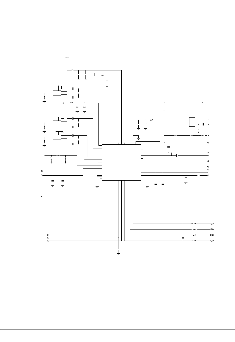
5. SGH-D500 BlockDiagrams
5-1
1.RFSolutionBlockDiagram
SAMSUNG Proprietary-Contents may change without notice
BlockDiagrams
ThisDocumentcan notbe used withoutSamsung'sauthorization
5-2
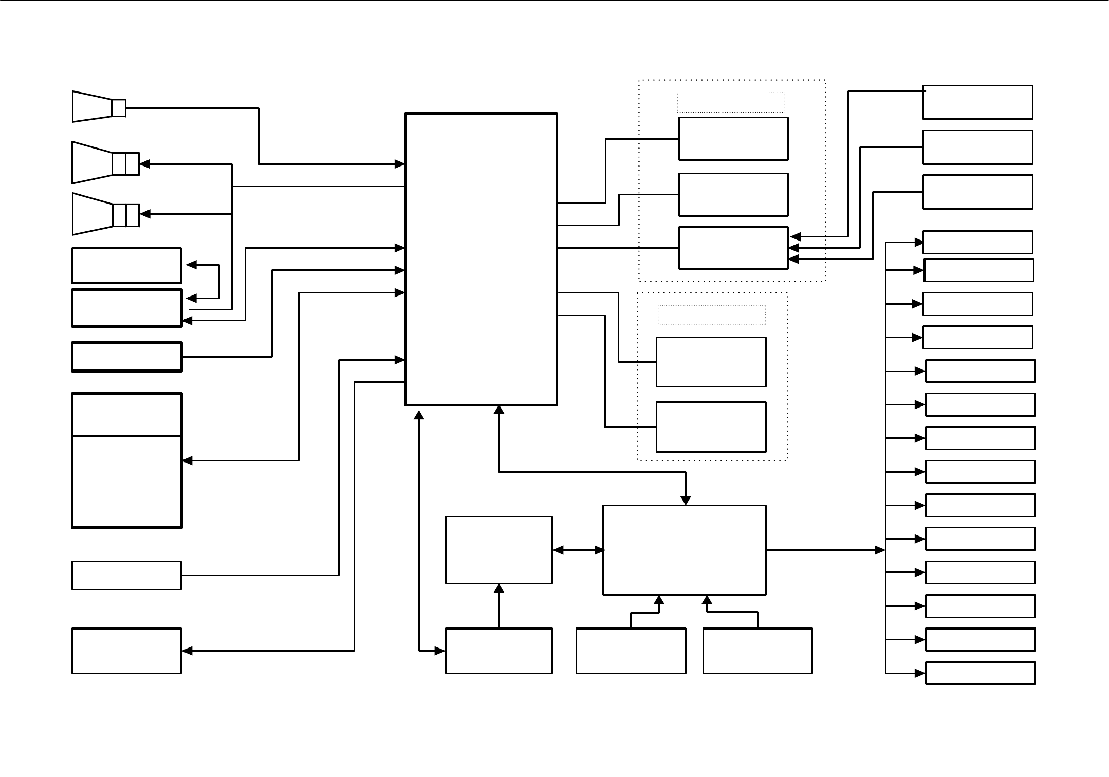
2.Base Band SolutionBlockDiagram
Battery
Type
Battery
Voltage
Battery
Temperature
AFC
RAMP
Charging Circuit
Li-Ion Battery
(Slim,Standard)
PCF5213EL1
VIBRATOR
SYSTEM CLOCK
(26MHz)
RTC_CLOCK
(32.768KHz)
KEY_BOARD
RECEIVER
MIC
LCD
RF INTERFACE D3VDD
AVDD
VINT
PMU
D2VDD
Serial Data
Interface
I/O
Interface
A/D
Interface
BB INTERFACE
MELODY IC
(64 Poly)
SPEAKER
IOVDD
VDD_RX_TX
VCC_SYN
MIC_BIAS
CPVDD
D1VDD
SIMEN
GPO
VCHG
VSAVE
SIM CARD
MV319DNQ
Ext.
SPEAKER
1G OneNAND
MEMORY
SAMSUNG Proprietary-Contents may change without notice
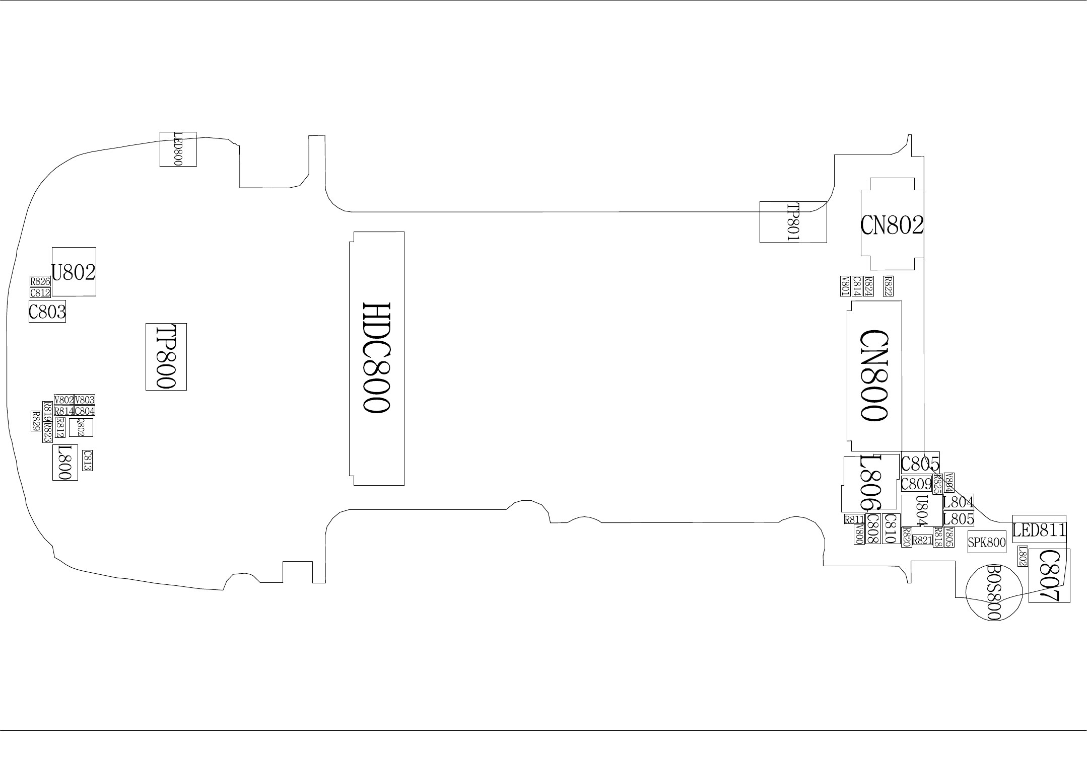
6. SGH-D500 PCB Diagrams
6-1
ThisDocumentcan notbe used withoutSamsung'sauthorization
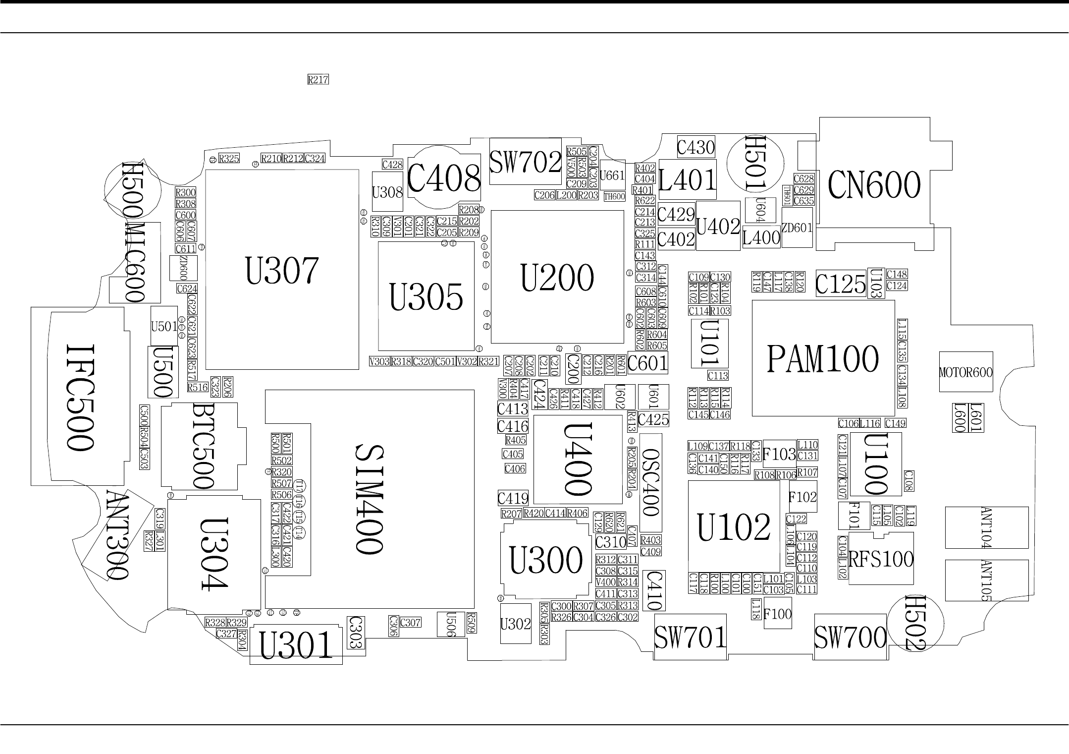
1.MainPCB TopDiagram
SAMSUNG Proprietary-Contents may change without notice
PCB Diagrams
6-2
ThisDocumentcan notbe used withoutSamsung'sauthorization
2.MainPCB BottomDiagram
SAMSUNG Proprietary-Contents may change without notice
PCB Diagrams
6-3
ThisDocumentcan notbe used withoutSamsung'sauthorization
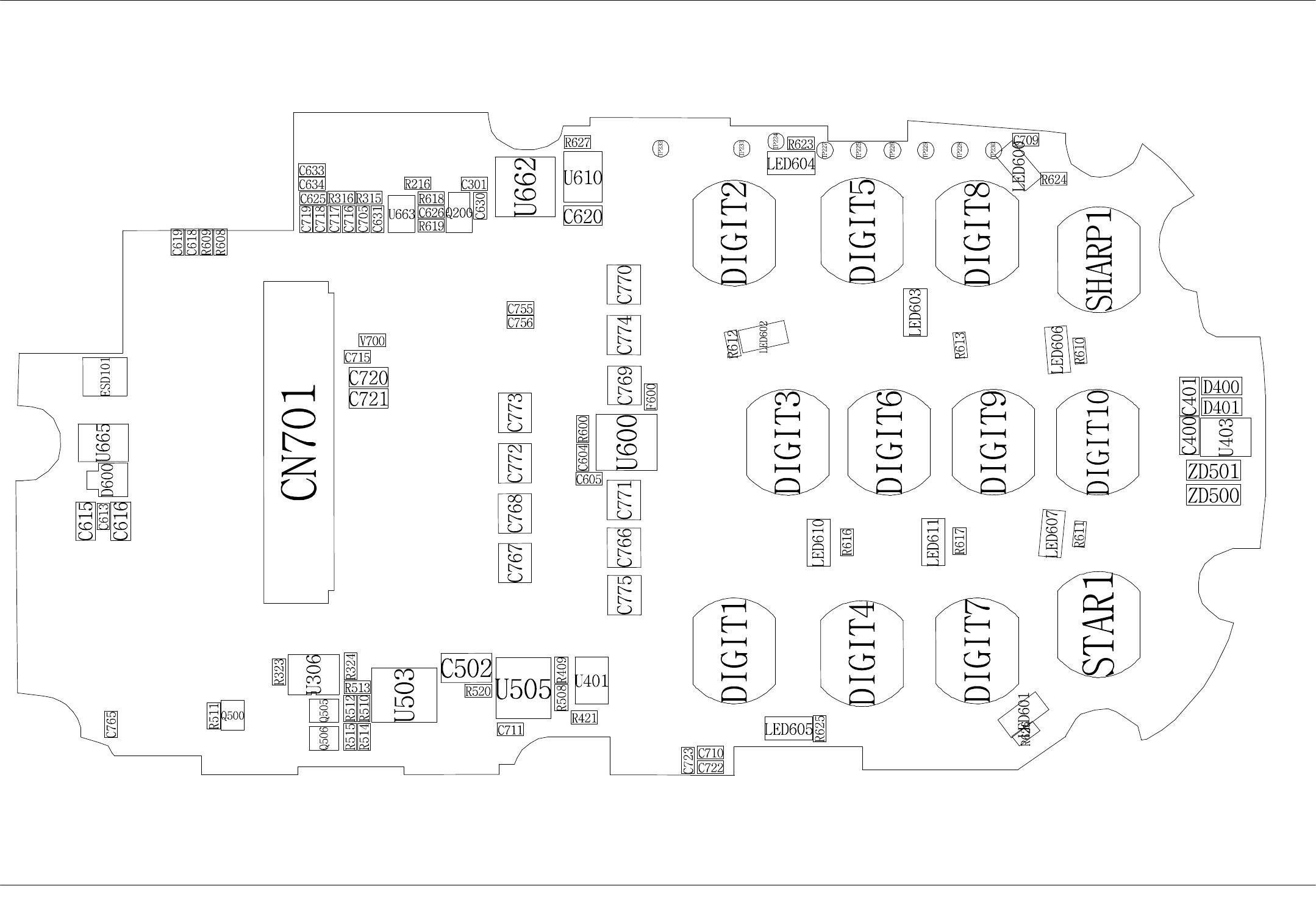
3.Sub PCB TopDiagram
SAMSUNG Proprietary-Contents may change without notice
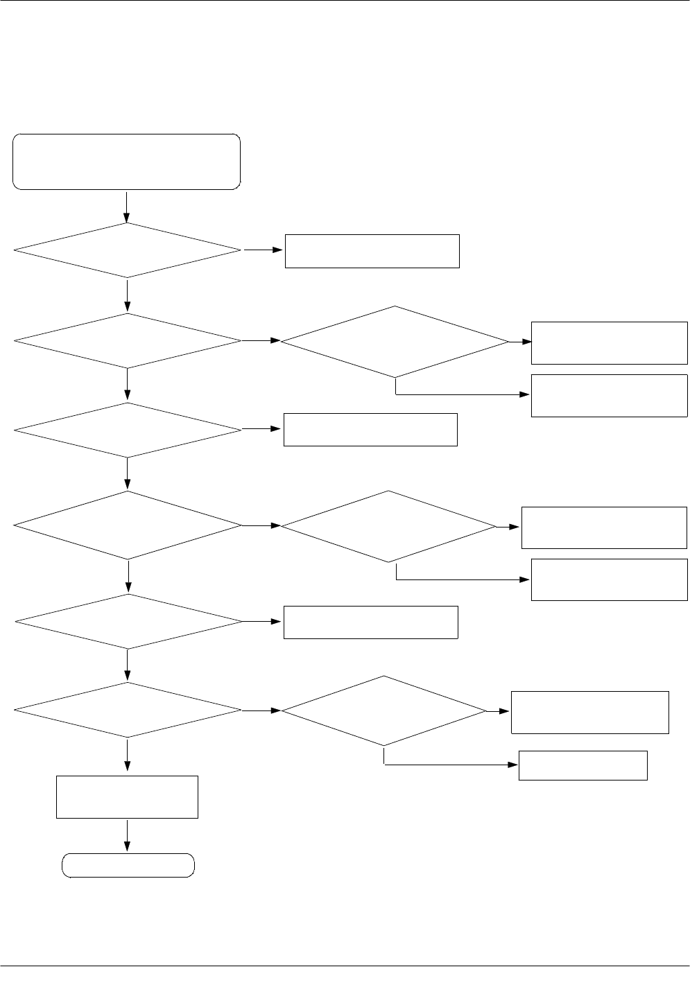
7. SGH-D500 FlowChart of Troubleshooting
ThisDocumentcan notbe used withoutSamsung'sauthorization
7-1
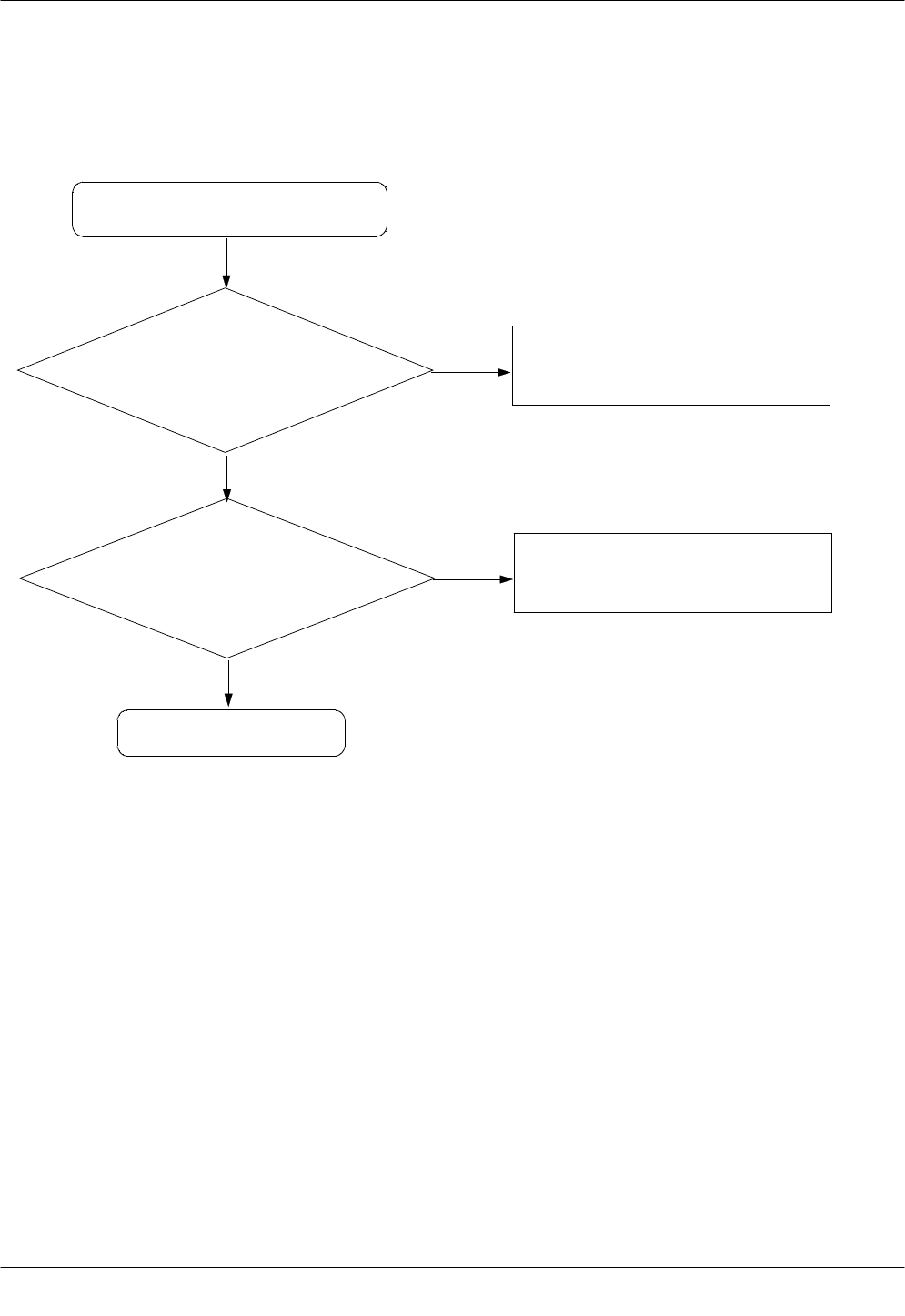
1. Power On
ChecktheBatteryVoltage
ismorethan3.4V
'PowerOn'doesnotwork
ChangetheBattery
END
No
Yes
C406(VINT)=2.7V?CheckthePMUrelated toVINT
No
Yes
ChecktheClockat
R403=32KHZResolderOSC400
No
Yes
C427(+VDD_IO_LOW)&
C426(+VDD_IO_HIGH)="H"?Checktherelated circuit
No
Yes
C403(+VDD_GSM_CORE)
=1.8V?
Checkthe+VDD_GSM_CORE circuit
No
Yes
CheckfortheclockatC129
=26MHz
Checktheclockgenerationcircuit
(related toU101)
No
Yes
Checktheinitialoperation
Yes
Yes
SAMSUNG Proprietary-Contents may change without notice
ThisDocumentcan notbe used withoutSamsung'sauthorization
FlowChartofTroubleshooting
7-2
SIM_VCC
SIM_CL K
SIM_RST
SIM_IO
ML-414RM/F9M E
C408
470nF
C426
4.7U F
C424
9 10
G
MC-146(32.768KHz,20ppm )
OSC400
2
3 4
1
2 2
33 4 4
5
5
6 6
G
7 8
G G
C417
470nF
ENG-CD-292292-9-OLD 2
SIM400
11
T400
100K
R421
C411
33PF
470nF
C418
C428
100PF
R412
0
R413
51 0
11 K
9PF
C407
R409
C425
4.7U F
5
4
+VDD_IO_HIGH
TC7SH08FU-TE85L
U401
3
1
2
NC
C421
C419
4.7U FN C
C422
R404
0
C413
4.7U F
4.7U F
C416
C405
100N F
C420
100N F
R405
22U F
C410
F95OJ226MPAAQ2
R403
33nH
+VDD_IO_LOW
10M
R411
+VDD_IO_HIGH
0
470nF
C406
R406
V400
VC040205X150R
_IRQ
27
_ONKEY
1
_REC1
13 _REC 2
11
_RSTH
C
44
_SIMRSCD
7
_SIMRSH
C
100K
SIMEN
42
SIMIOCD
9
SIMIOHC
41
SIMVCC
31
VBAT
32
VCHG
29
VINT
30
VSAVE
10 2
SCL
38
SCN
37
SCP
3
SD
A
43
SIMCKCD
8
SIMCKH
C
40
SIMD3VBAT
45
26
OSCI
25
OSCO
6
PWREN
1
5
PWREN
2
28
REFC
23 RF12VBAT
RF1VDD
22
24 RF2VDD
17 HCVDD
15 IOD2VBAT
IOVDD
14
LPD1VBAT
20
19 LPVD D
12
MICBIAS
53
NC
NC 54
D3VDD
49
GND
GND 50
51
GND
GND 52
48
GPO1
47
GPO2
46
GPO3
HCVBAT
18
34
CHGCUR/BATMA
X
33
CHGDRV
4
CLK32K
36
CPVBAT
35
CPVD
D
21 D1VD D
D2VD D
16
39
PCF50603HN/11
U400
470nF
C427
C409
9PF
C414
470nF
IT_PM U
ONKEYN
AUX_ON
RSTON
SIMRST
SCV_LED_ON
REF_O N
PON_TX
SC L
SD A
SIMCL K
SIMIO
VBAT
+AVDD
+AVDD_HFA
+VDD_IMAGE
32KHz_DIGIT
VDD_SLEE P
LCD_BL_ON
BACKLIGHT
MIC_BIAS
+VDD_RX_TX
+VCC_SYN
+VDD_IO_HIGH
+VDD_IO_LOW
SAMSUNG Proprietary-Contents may change without notice
FlowChartofTroubleshooting
ThisDocumentcan notbe used withoutSamsung'sauthorization
7-3
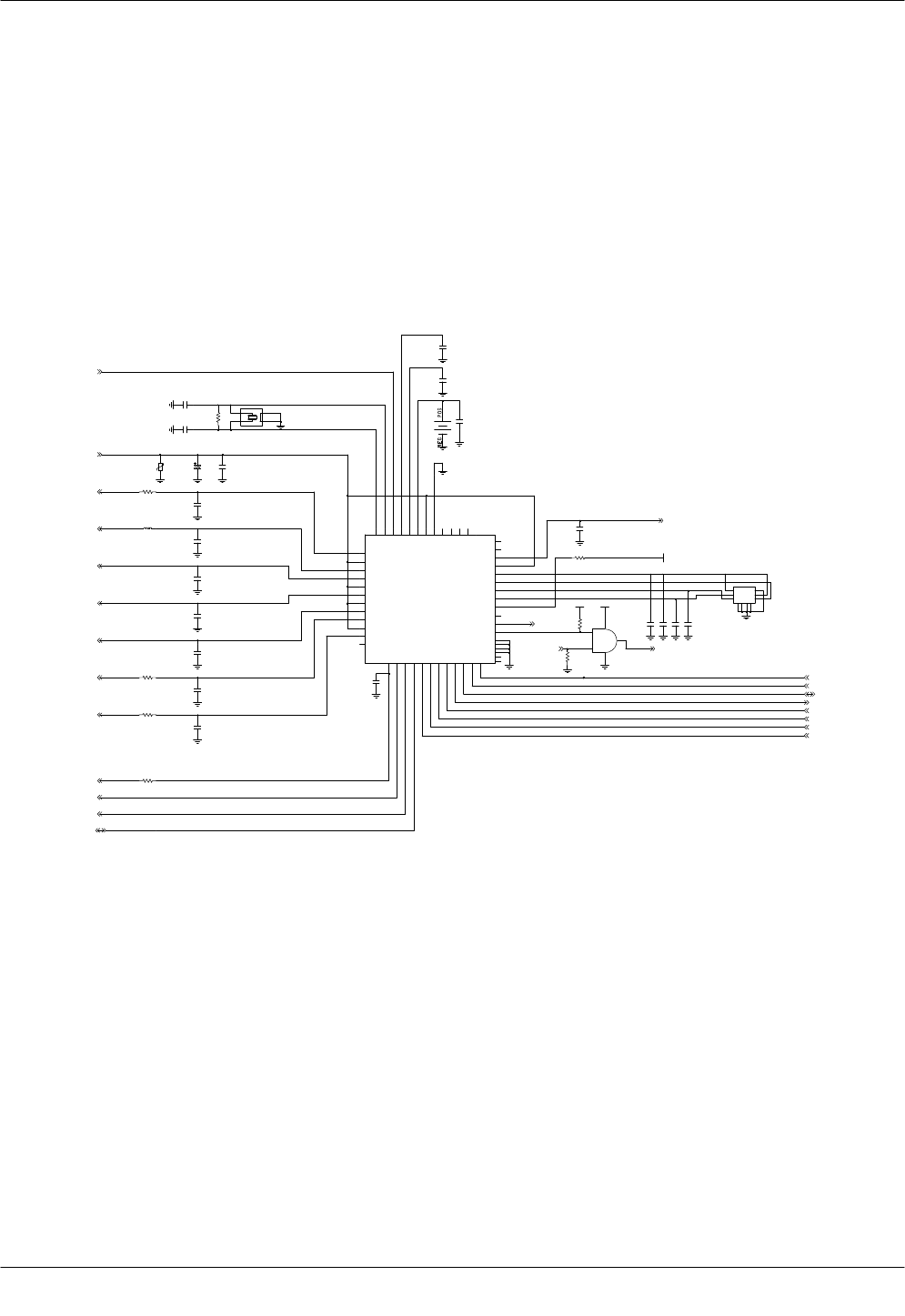
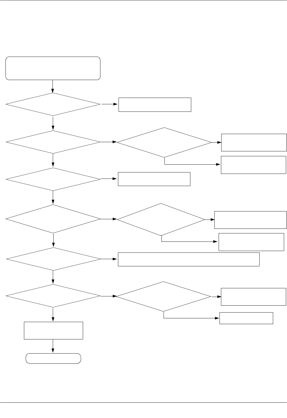
2. Initial
Q200 pin2(RSTON)="H"?
InitialFailure
Checkthecircuitrelated toreset
END
No
Yes
IsU308 pin4
OK?
Yes
Yes
NoChecktheU308
Checkthe16bitdatasignal
&memoryCE
Yes
SAMSUNG Proprietary-Contents may change without notice
ThisDocumentcan notbe used withoutSamsung'sauthorization
FlowChartofTroubleshooting
7-4
+VDD_IO_LO W
L200
JTAG
DAI & Bluetooth data Interface
USB Interface
TP208
+AVDD
TP207 C215
NC
0
R212
TP217
TP211
+VDD_USB
TP200
+VDD_IO_HIGH
+VDD_IO_LO W
R216
8.2K
TP216
+VDD_IO_HIGH
+VDD_IO_LO W
TP232
C200
4.7UF
+VDD_IO_LOW
R210
4.7K
TP222
NC
R203
+VDD_IO_LO W
TP202
TP215
TP204
TP231
TP201
TP203
R201 10K
+VDD_GSM_CORE
R206 100 K
R20 5
1.5 K
+AVDD
TP229
+VDD_IO_LO W
100K R207
TP210
R209
100K
+AVDD_HFA
+VDD_IO_HIGH
100N F C216
R202
0
TP226
1.5K
R20 4
TP227
TP230
TP220
GPIOA29 V3
GPIOA31 V4
GPIOA3 V5
VSSBB
V6
QP V7
QN V8
VSSA4
V9
MICBIAS
V12
VDDV
B V13
HDP11
V14 HDP10
V15
CLK32O
V16
HDP
2
V17
RFEN 0 V18
GPIOA17 V2
GNDC
U5
VDDB
B U6
IP U7
IN U8
VSSCLK
U9
GPIOB10
V1
MCLK V10
AUXDAC3 V11
VREF
U14
HDP
0
U1
5
RSTEXT
U1 6
SCL U17
RFCLK1
U18
VDDE
2 U2
GNDE
U3
GPIOA6
U4
VDDE
2 T17
VDDE
2 T18
GPIOA21 T2
GPIOA13
U1
VDDCLK U10
VDDE
2 U11
GNDE
U1
2
VSSREF
U1
3
GPIOA22 R2
GPIOB9
R4
GPIOA23 R5
GPIOA28 R6
VDDC R7
AUXDAC2 R8
AUXDAC1 R9
GPIOA25 T1
VDDRE
F R10
RFSIG6
R11
GNDC
R12
RFSIG0
R13
HDP
7
R14
HDP
8
R15
RFDO1 R17
GNDE
R18
GNDE
P2
GNDE
P4
GPIOA19
P5
GPIOA27 P6
GPIOB8
P7
GPIOA30 P8
GPIOA4 P9
GPIOB5
R1
GPIOA2 P10
RFSIG7
P11
VDDC P12
VSSA5
P13
HDP
9
P14
HDP
1
P15
GNDE
P17
HDP
5
P18
SIMPW R N14
HDP12
N1
5
HDP
3
N1
7
MICP N18
VDDE
2 N2
VDDE
2 N4
TXD
1 N5
GPIOA16
P1
MICN M1 8
GNDC
M2
VDDC M4
GPIOA0
M5
GPIOA1 M7
GPIOA11 M8
VDDE
1 M9
GPIOA24 N1
GPIOA26 L9
GPON 1 M1
GNDE
M1
0
RFSIG2
M1 1
RFSIG1
M1 2
SD A M1 4
VDDC M15
AUXMICP
M1 7
MCLKSEL
L15
AUXMICN L17
AN R L18
AUXADC5 L2
TCK
L4
TD
O
L5
GPIOA18
L7
GPIOA15
L8
TM
S
K5
GPIOA14
K7
NC K8
AUXADC4 L1
GPIOA10 L10
GPIOA5 L11
HDP
4
L12
GPIOB11
L14
GPIOA20
K11
JSEL
K12
GNDC
K14
EAR1 K1 5
VSSVBO
K17
ANL K1 8
AUXADC3 K2
CS 3
K4
HFR1 J17
NC J18
GNDE
J2
GPIOA7
J4
BE1
J5
ADD0_BE0
J7
ADD1_BE2
J8
AUXADC2 K1
AD V
H7
GPON 0 H8
VDDE
1 H9
AUXADC1 J1
GPIOA12
J11
VDDE
1 J12
HDP
6
J14
EAR2 J15
VDDE
4 H12
VSSVB
H1
4
VDDE
3 H15
BBPW
R H17
HFR2 H18
VDDE
1 H2
GPIOA8
H4
CS 1
H5
WE_E
G4
BE3 G5
IO9
G7 IO8
G8
GNDE
G9
RESET H1
GNDE
H1
0
USBDP H11
TD
I
G1
0
TRST
G1
1
RSTBB
G12
USBDM
G14
VDDE
1 G1
5
SIMCLK
G17
VDDVBO G1
8
CS 0
G2
USBCN F14
GNDE
F15
SIMRST
F17
RTCK
F18
GPIOB2
F2
ADD2 1
F4
ADD2 3
F5
GPIOA9 G1
OE_R_W
E2
IO28
E4
IO29
E5
IO31
E6
IO4
E7
IO7
E8
VDDE
1 E9
ADD2 0
F1
NC E10
DCL E11
NC E12
RSTRTC
E13
VDDE
1 E14
GNDE
E15
KCOL3
E17
NC E18
GNDE
D2
IO24
D4
IO25
D5
VDDE
1 D6
GNDE
D7
IO11
D8
IO3
D9
ADD2 1
E1
IO5
D1 0
GNDE
D1
1
GNDE
D1
2
FS C D1 3
NC D1
4
SIMIO D1 5
KCOL2
D1 7
KCOL0
D1 8
IO6
B7
IO2
B8
IO13
B9
IO27
C1
KROW 2
C17
KCOL1
C18
VDDE
1 C2
IO19
D1
XIN32K
B16
KROW 3
B17
KCOL4
B18
IO21
B2
IO30
B3
IO26
B4
IO23
B5
IO15
B6
IO16
A9
ADD1 9
B1
NC B10
VDDC B11
GNDC
B12
DD B1 3
DU B1 4
XOUT32K
B15
KROW 1
A18
IO18
A2 IO17
A3
IO22
A4
ADD1 8
A5
IO14
A6
IO12
A7
IO10
A8
IO0
A10
IO1
A11
GNDE
A1
2
VDDA2 A1
3
CK I
A14
VDDRTC A1
5
KROW 0
A16
KROW 4
A17
U200
PCF5213EL1/044/3
1
NC
2
NC
IO20
A1
TP225
SI1012R
Q200
D 3
G 1
S 2
TP219
TP205
TP22 1
TP213
100K
R208
TP209
+AVD D
TP228
TP206
NC
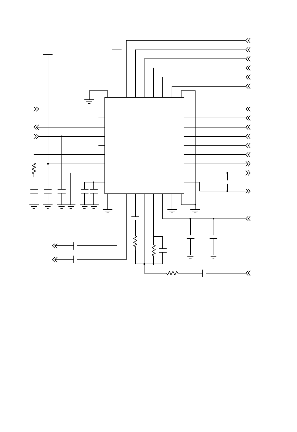
+VDD_GSM_CORE
TP212
+VDD_IO_LOW
R217
J_SE L
SC L SD A
AN R
AN L
TRSTn
LCD_RESET
RSTON
RTCK
RSTO N
CS2n_FLASH
RTCK
TRCCLK
TEMP_PRODUCT
EXTSPK_EN
LOUD_EN
EAR_SWITCH
EAR2
EAR1
EXT1
SIMRST
SIMIO
SIMCLK
FLASH_EN
END_OF_CHG
CHG_ON
MELODY_SEL
AFC
D_REF_CLK
RF_EN
EAR_ADC
MES_BATT
DD
DC L
AUXMICN
MIC_N
MIC_P
M_INT
IT_PMU
PON_PA
PON_SW
MODE_SELECT
RX_TX_IN
RX_TX_IP
RX_TX_QN
RX_TX_QP
MIC_BIAS_B B
RAMP
IMAGE_IN T
RXD 2
REF_ON
DC S
PON_3587_SYNTH
PON_TX
BT_INT
JACK_EN
DU
HFR_N
RF_DATA
RF_CLK
BT_RST
HFK_SPK_EN
EXT2
SLIDER_KEY_ON
JACK_IN
CS4n_NAND
USB_CHG_O N
RSTEXTn
IMAGE_RESET
GPON 1
VF
HA(24)
LCD_BL_ON
USBDM
USBDP
CLKBURS T
HA(21)
HA(0)
EDGE1_P A
AUXMICP
FSC
TXD2
KEY_LED_ON
HFR_P
USBCN
HA(12)
HA(13)
HA(14)
HA(15)
HA(16)
HA(17)
HA(18)
HA(19)
HA(20)
HA(23)
HA(22)
HA(2)
HA(3)
HA(4)
HA(5)
HA(6)
HA(7)
HA(8)
HA(9)
HA(10)
HA(11)
TRCPKT(2)
TRCPKT(1)
TCK
TDI
TDO
TMS
PIPESTAT(0:2)
TRCPKT(0:7)
KEY_ROW(0:4)
KEY_ROW(4)
KEY_ROW(3)
KEY_ROW(2)
KEY_ROW(1)
KEY_ROW(0)
HA(0:23)
HA(1)
CS5n_MELODY
BB_PW R
PIPESTAT(2)
PIPESTAT(1)
TRCPKT(0)
TRCSYN C
PIPESTAT(0)
TRCPKT(7)
TRCPKT(6)
TRCPKT(5)
TRCPKT(4)
TRCPKT(3)
CS3n_IMAG E
USB_IN
FLIP
RXD1
WAITn
OEn
RSTEXTn
TXD
1
WE n
32KHz_DIGIT
HD(9)
HD(10)
HD(11)
HD(12)
HD(13)
HD(14)
HD(15)
ADVn
BE1n
CS0n_FLASH
CS1n_RAM
KEY_COL(3)
KEY_COL(4)
HD(0:15) HD(0)
HD(1)
HD(2)
HD(3)
HD(4)
HD(5)
HD(6)
HD(7)
HD(8)
KEY_COL(0:4)
KEY_COL(0)
KEY_COL(1)
KEY_COL(2)
SAMSUNG Proprietary-Contents may change without notice
FlowChartofTroubleshooting
ThisDocumentcan notbe used withoutSamsung'sauthorization
7-5
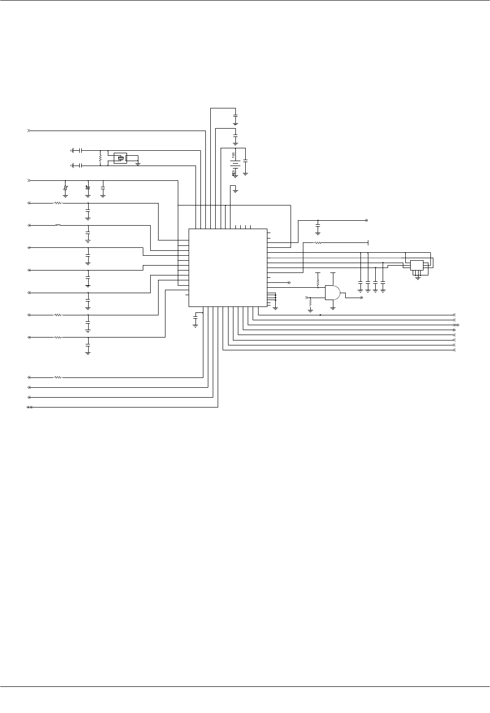
3. ChargingPart
ChecktheU503 pin6
>4.9V
Abnormalchargingpart
END
No
Yes
U503 pin8="L"?No
Yes
Q201 pin1(AUX_ON)
="L"?
No
Yes
ChecktheU503 pin2
≒4.2V
No
Yes
Checkthecircuitrelated to
V_EXT_CHARGE
Resolderor replaceU503
Checkthecircuitrelated to
AUX_ONsignal
Resolderor replaceU503
Yes
SAMSUNG Proprietary-Contents may change without notice
ThisDocumentcan notbe used withoutSamsung'sauthorization
FlowChartofTroubleshooting
7-6
2.7K
68K
R513
1%
BATTERY CHARGING
1
3
2
+VDD_IO_HIGH
DTC144EM
Q505
62K,1%
R507
R515
330N F
C501
B2
C1
6
3
C2
E1 1
4 E2
U506
PEMD1 0
2
B1
5
100K
R520
R506
UDZS8.2B
ZD501
100K,1%
Q506
DTC144EM
1
3
2
100K
100K R508
R509
+VDD_IO_HIGH
3
2
R511
18K
1
5 VOU T
DTC144EM
Q500
1
FDC6332L
3
G1/G2
4 GND
2
ON/OFF
S1/S2
6 VI N
8
_EN
U505
11
GG
12
4 GND
1 ITERM
PRO G 5
6
VCC
_ACPR 7
_CHRG
3
U503
LT4068EDD-4. 2
2 BAT
9
GG
10
100NF
C503
2K
R510
C502
F951A106MPAAQ 2
VBAT
1K,1%
R514
UDZS5.1B
ZD500
R512
4.7K,1%
CHG_O N
END_OF_CHG
AUX_O N
+VBUS
USB_CHG_O N
+VBUS
V_EXT_CHARGE
MES_BATT
USB_CHG_ON
USB_IN
+VDD_IO_HIGH
+VBU S
SAMSUNG Proprietary-Contents may change without notice
FlowChartofTroubleshooting
ThisDocumentcan notbe used withoutSamsung'sauthorization
7-7
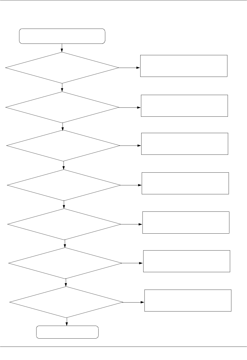
4. SimPart
SIM400 pin1,5="H"?
Phonecan'taccess SIMCard
Checkthesimchargepump
ChecktheSIMCard
END
No
Yes
Yes
Yes
No
ChecktheClock
AfterPowerON,
CheckSIMCLKSignalon
pin3ofSIM400 inafewsecond
Yes
No
ReplacePBA
AfterSIMcardinsert,
SIM400 pin2="H(SIM_RST)"?
Yes
SAMSUNG Proprietary-Contents may change without notice
ThisDocumentcan notbe used withoutSamsung'sauthorization
FlowChartofTroubleshooting
7-8
SIM_VCC
SIM_CL K
SIM_RST
SIM_IO
ML-414RM/F9M E
C408
470nF
C426
4.7U F
C424
9 10
G
MC-146(32.768KHz,20ppm )
OSC400
2
3 4
1
2 2
33 4 4
5
5
6 6
G
7 8
G G
C417
470nF
ENG-CD-292292-9-OLD 2
SIM400
11
T400
100K
R421
C411
33PF
470nF
C418
C428
100PF
R412
0
R413
51 0
11 K
9PF
C407
R409
C425
4.7U F
5
4
+VDD_IO_HIGH
TC7SH08FU-TE85L
U401
3
1
2
NC
C421
C419
4.7U FN C
C422
R404
0
C413
4.7U F
4.7U F
C416
C405
100N F
C420
100N F
R405
22U F
C410
F95OJ226MPAAQ2
R403
33nH
+VDD_IO_LOW
10M
R411
+VDD_IO_HIGH
0
470nF
C406
R406
V400
VC040205X150R
_IRQ
27
_ONKEY
1
_REC1
13 _REC 2
11
_RSTH
C
44
_SIMRSCD
7
_SIMRSH
C
100K
SIMEN
42
SIMIOCD
9
SIMIOHC
41
SIMVCC
31
VBAT
32
VCHG
29
VINT
30
VSAVE
10 2
SCL
38
SCN
37
SCP
3
SD
A
43
SIMCKCD
8
SIMCKH
C
40
SIMD3VBAT
45
26
OSCI
25
OSCO
6
PWREN
1
5
PWREN
2
28
REFC
23 RF12VBAT
RF1VDD
22
24 RF2VDD
17 HCVDD
15 IOD2VBAT
IOVDD
14
LPD1VBAT
20
19 LPVD D
12
MICBIAS
53
NC
NC 54
D3VDD
49
GND
GND 50
51
GND
GND 52
48
GPO1
47
GPO2
46
GPO3
HCVBAT
18
34
CHGCUR/BATMA
X
33
CHGDRV
4
CLK32K
36
CPVBAT
35
CPVD
D
21 D1VD D
D2VD D
16
39
PCF50603HN/11
U400
470nF
C427
C409
9PF
C414
470nF
IT_PM U
ONKEYN
AUX_ON
RSTON
SIMRST
SCV_LED_ON
REF_O N
PON_TX
SC L
SD A
SIMCL K
SIMIO
VBAT
+AVDD
+AVDD_HFA
+VDD_IMAGE
32KHz_DIGIT
VDD_SLEE P
LCD_BL_ON
BACKLIGHT
MIC_BIAS
+VDD_RX_TX
+VCC_SYN
+VDD_IO_HIGH
+VDD_IO_LOW
SAMSUNG Proprietary-Contents may change without notice
FlowChartofTroubleshooting
ThisDocumentcan notbe used withoutSamsung'sauthorization
7-9
5. MicrophonePart
Checktheconnection
fromMIC
Checkthecircuit
fromU200 toMIC
ResolderMIC
ResoldertheC603,C609,R602,R604,R605
END
No
Yes
Yes
Yes
Yes
No
CheckU601,U602 PIN1
='H'?NoChecktheJACK_ENsignal
Microphone doesnotwork
Yes
ChecktheMICNoReplacetheMIC
SAMSUNG Proprietary-Contents may change without notice
ThisDocumentcan notbe used withoutSamsung'sauthorization
FlowChartofTroubleshooting
7-10
EARPIEC E
MICROPHONE
Close to MCP
Close to microphone
510
R60 5
5P F C62 9
6.3V
22UF
C601 R601
NC
100N F
VBAT
C60 3
180K
+VDD_IO_HIG H
R60 9
6
7 7
88
9 9
11
G G
12 13
G G
14
1 1
10 10
22
3 3
44
5 5
6
CN600
1747124-1
+VDD_IO_HIG H
TH60 0
VC040205X150R
GND
17
GND
NC
21
22 NC
14
V+
9
3S 2
11
4S1
13
4S2
D1
16
4 D2
D3
8
D4 12
6
U662
STG3699
2 1-2IN
15
1S1
1 1S 2
2S 1
3
5
2S2
3-4I N 10
3S1
7
U602
DG2011
COM 5
GND
3
IN
1
4
NC
6
NO
2 V+
ZD601
ESDA6V1-5W 6
1 2 3
4 5
6
10PF
MIC_BIA S
C600
47PF
C619
+VDD_IO_HIG H
R603
12PF
R608
100K
10NF
C62 5
C626
10NF
5P F
C628
NO 6
V+
2
DG201 1
U60 4
5
COM
3 GND
1 IN
NC 4
10PF
C611
C60 8
68PF
C609
100NF
C63 3
C63 0
9P F
18PF
+AVDD_HF A
C602
NC
VC040205X150R
TH60 1
1.8PF
C606
1
3
5
4
TC75S56F E
U663 2
5
COM
3 GND
1 IN
NC 4
NO 6
V+
2
DG201 1
U66 1
R621
100K
MIC_BIAS_B B
100N F
C631
1K
R60 4
4
NO 6
V+
2
DG2011
U601
5
COM
3 GND
1 IN
NC
R60 2
1K
R622 10 0
3
4 5
6
78
MIC_BIA S
GMF05C-HS 3
ZD600
1 2
MIC_BIAS
R61 9
130K,1%
9PF
C63 5
C634 18PF
MIC600
C60 7
27PF
R62 0
R618
330K,1%
39 K
C61 0
NC
C618
8PF
EAR_ADC
EARSPK_L
EARSPK_COM
EAR1
HFR_N
JACK_EN
EARSPK_R
AMP_ N
EARSPK_R
EARSPK_COM
EXTSPK_E N
EARP_HF LOUD_EN
EAR_SWITC H
EARSPK_
L
EAR_P
HFK_SPK_EN
HFK_SP K
EAR_ P
AMP_P
EAR2
AMP_ N
SPK_ N
SPK_P
MELODY_SEL
AMP_P
HFR_P
HFR_N
JACK_IN
MIC_N
MIC_P MIC_CP
SAMSUNG Proprietary-Contents may change without notice
FlowChartofTroubleshooting
ThisDocumentcan notbe used withoutSamsung'sauthorization
7-11
6. Speaker Part(Melody)
U302 pin5=2.9V?
Speakerdoesnotwork
ChecktheClocksignalat
Pin1ofU300 (26MHz)
Checktheclockgenerationcircuit
(related toU101andU300)
No
Yes
No
Resolderor replaceU303
Yes
U300 pin17,18 ≒1.8V?
(WhenU300 operate)ResolderU300
No
Yes
No
END
HDC800 pin3,5≒1.8V?
(WhenU300 operate)
Changethe boardtoboard
FPCB
IsSpeakerworking?ChangetheSpeaker
No
Yes
Yes
Yes
CN701 pin51,53 ≒1.8V?
(WhenU300 operate)ResolderCN701
No
Yes
SAMSUNG Proprietary-Contents may change without notice
ThisDocumentcan notbe used withoutSamsung'sauthorization
FlowChartofTroubleshooting
7-12
CODE C
MELODY IC
C301
27P F
+VDD_IO_HIG H
3.3K
R307
10K
R312
1N F
C304
R313
39K
33N F C315
/W
R
39N F
C311
7 VDD
9 VREF
8 VSS
/C
S
29
3
/IRQ
/RD 31
/RST
4
28
32
LED
2
19
MT R
5 NC
PLLC
6
17
SPOUT1
SPOUT2 18
15
SPVD
D
SPVSS
16
EQ
2
EQ
3
14
G 33
34
G
G
35
36 G
HPOUT-L/MONO
10 11
HPOUT-R
IOVD
D
D1
25
D2
D3 24
23
D4
D5 22
21
D6
D7 20
EQ
1
12 13
YMU765
U300
30
A0
1 CLKI
D0
27 26
15K
R314
3.9NF
C326
100NF
C312
C325
100N F
+VDD_IO_LOW
C314
100NF
C313
560PF
100N F
C305
10V
1UF
C310
C302
100NF
100N F
C308
EARP_H F
VBAT
AN L
ANR
AMP_P
HD(7)
VIB
AMP_N
HD(4)
M_INT
HD(5)
RSTON
HD(6)
HD(1)
HD(0)
WE n
CS5n_MELODY
HA(1)
OEn
HD(2) 26M_DIGIT
HD(3)
SAMSUNG Proprietary-Contents may change without notice
FlowChartofTroubleshooting
ThisDocumentcan notbe used withoutSamsung'sauthorization
7-13
7. KeyDataInput
Whenoneofthekeysis
pushed,
isitdisplayed onLCD?
ChecktheDomesheet&KeyPad
END
No
Yes
Yes
CheckInitialOperation
Whenoneofthekeysis
pushed,
KBIOsignalisOK?
ReplacethePBA
No
Yes
SAMSUNG Proprietary-Contents may change without notice
ThisDocumentcan notbe used withoutSamsung'sauthorization
FlowChartofTroubleshooting
7-14
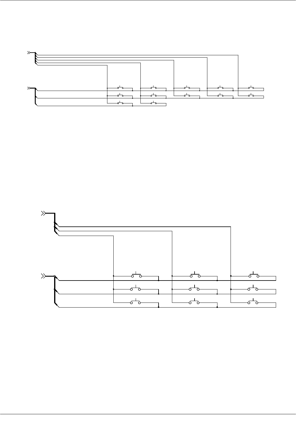
KEY_MAP
DIGIT5
12
DIGIT10
12
DIGIT9
12
12
DIGIT4 STAR1
12
DIGIT3
12
DIGIT8
12
DIGIT1
12 12
SHARP1
12
DIGIT7
12
DIGIT6
2
DIGIT2
1
KEY_COL(0:4)
KEY_ROW(0)
KEY_COL(4)
KEY_COL(3)
KEY_COL(2)
KEY_ROW(1)
KEY_COL(1)
KEY_COL(0)
KEY_ROW(0:2)
KEY_ROW(2)
KEY_MAP
RIGHT
1 2
IN T
1 2
DOWN
1 2
1 2
LEFT
SOFT2
1 2
SOFT1
12
UP
1 2
CL R
12
SEN D
12
KEY_COL(3 )
KEY_COL(2 )
KEY_COL(2:4 )
KEY_COL(4 )
KEY_ROW(2:4)
KEY_ROW(3)
KEY_ROW(2)
KEY_ROW(4)
SAMSUNG Proprietary-Contents may change without notice
FlowChartofTroubleshooting
ThisDocumentcan notbe used withoutSamsung'sauthorization
7-15
8. Receiver Part
U662 pin2,10 =1.5V?ResolderU200 orchangePBA
END
No
Yes
Yes
Receiverdoesnotwork
SPK+,-PAD=1.5V?ChangetheSlide board
No
Yes
IsReceiverworking?ReplacetheSpeaker
No
Yes
No
Resolderor replaceU662
Yes
No
changeU200
CN701 pin51,53=1.5V?
Yes
HDC200 pin3,5=1.5V?
NoChangethe boardtoboard
FPCB
Yes
Checkthesoldering ofthe
spaeakerwire
No
Modifythespeakerwiresoldering
Yes
U662 pin4,16 =1.5V?
SAMSUNG Proprietary-Contents may change without notice
ThisDocumentcan notbe used withoutSamsung'sauthorization
FlowChartofTroubleshooting
7-16
VBAT
+VDD_IO_HIG H
GND
17
GND
NC
21
22 NC
14
V+
9
3S 2
11
4S1
13
4S2
D1
16
4 D2
D3
8
D4 12
6
U662
STG3699
2 1-2IN
15
1S1
1 1S 2
2S 1
3
5
2S2
3-4I N 10
3S1
7
C626
10NF
R61 9
130K,1%
R618
330K,1%
HFR_N
AMP_ N
EARSPK_R
EARSPK_COM
EXTSPK_E N
EAR_ P
AMP_P
AMP_ N
SPK_ N
SPK_P
MELODY_SEL
AMP_P
HFR_P
HFR_N
SAMSUNG Proprietary-Contents may change without notice
FlowChartofTroubleshooting
ThisDocumentcan notbe used withoutSamsung'sauthorization
7-17
9. BackLight (forColor MainLCD)
IsLCDContrastsetonhigh
levelintheMenu?SetLCDContrastonhighlevel
END
No
Yes
Yes
Backlightdoesnotwork
HDC800 pin10 =H?Changethe boardtoboard
FPCB
No
Yes
U802 PIN1=12V?ChecktheU601 &therelated circuit
No
Yes
Yes
ReplacetheLCDModule
SAMSUNG Proprietary-Contents may change without notice
ThisDocumentcan notbe used withoutSamsung'sauthorization
FlowChartofTroubleshooting
7-18
LCD BACKLIGHT
C812
33PF
10
R819
VBAT
C813
39N F
6 SW
VI N
5
VOUT 1
LT3465AES6
U802
4 CTRL FB 3
2
GND
NC
C804
R823
NC
22uH
L800
C803
220n F
50V
LED800
BACKLIGHT
SAMSUNG Proprietary-Contents may change without notice
FlowChartofTroubleshooting
ThisDocumentcan notbe used withoutSamsung'sauthorization
7-19
10. KeyBackLight
1)MainKeyPart
2)Sub KeyPart
C770 pin5(CN701 pin47)
="H"?ChecktheCN701 orReplacePBA
END
No
Yes
Yes
SubKeyLEDdoesnotwork
Q800 pin3="L"?
No
ChecktheQ800
Yes
U610 pin1="H"?ChecktheU200 related to"VDD_KEY"
END
No
Yes
Yes
MainKeyLEDdoesnotwork
CN800 PIN1="H"?Changethe boardtoboard
FPCB
No
Yes
SAMSUNG Proprietary-Contents may change without notice
ThisDocumentcan notbe used withoutSamsung'sauthorization
FlowChartofTroubleshooting
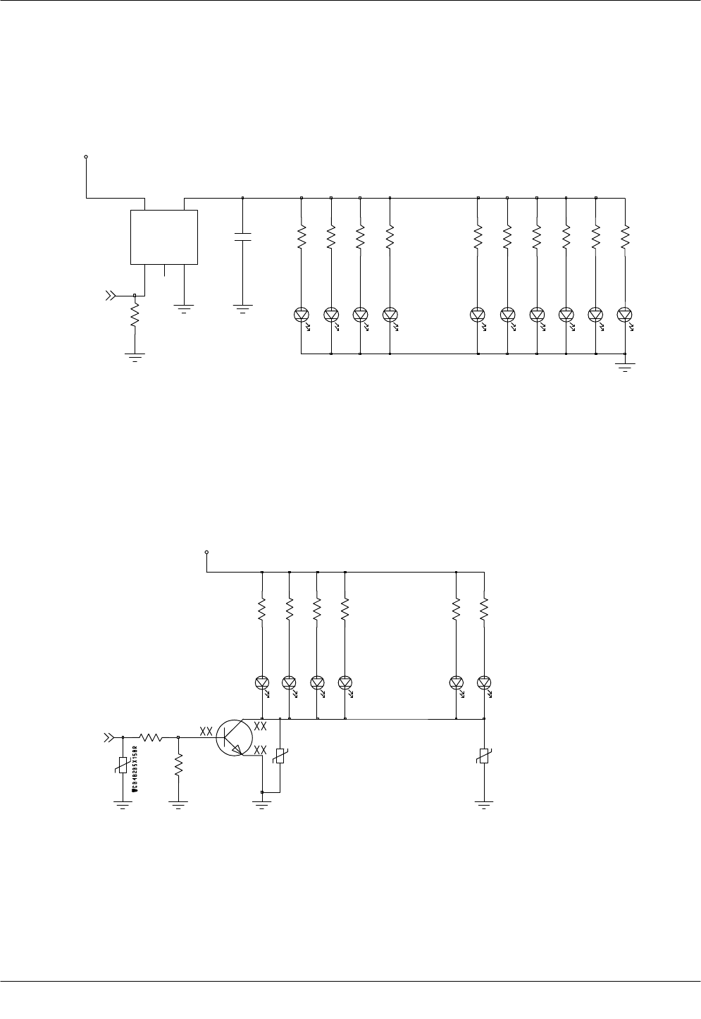
7-20
MOTOR
R616
82
R626
82
LED604
R62 3
82
LED60 2
R625
82
LED606 LED60 3
4.7U F
C620
LED60 0
R627
100K
R624
82
VBA T
3
GND N/ C
2
VE N
1
5
VIN VOUT
4
82
U61 0
LMS5214IMG-3. 3
LED60 5
R617
LED601
82
R612
LED610
82
R61 0 R613
82
LED611 LED607
R61 1
82
KEY_LED_ON
KEY_LED
R829
VC040205X150R
V802
100K
R814
15K
R812
LED805
R802
91
LED807
VBAT
LED808
91
R803
VC040205X150R
V803
LED801
R801
91 91
R807
Q802
2SC5658T2LR
LED810
R806
91
LED806
91
R800
SLIDER_KEY_O N
SAMSUNG Proprietary-Contents may change without notice
FlowChartofTroubleshooting
ThisDocumentcan notbe used withoutSamsung'sauthorization
7-21
11. Camerapart
"Camera"functiondoesnotwork
Yes
NoReconnect thecameramodule
ChecktheCamera
connectoronSlide PCB
Yes
R822 =1.9V?NoChecktheHDC800 (orC809)
Yes
C320 =26MHz? NoCheckU302(pin2,pin4)related to
26Mhz
andR318
Yes
Isthereanotherproblem?
END
Replacethecamera
module
Yes
SAMSUNG Proprietary-Contents may change without notice
ThisDocumentcan notbe used withoutSamsung'sauthorization
FlowChartofTroubleshooting
7-22
IMAGE_DSP
R316
4.7K
+VDD_IMAG E
C320
20PF
VC040205X150R
+VDD_IO_LOW
+VDD_IO_HIGH
R315
4.7K
T7
V301
VC040205X150R
+VDD_GSM_CORE
B8
A2
SVDD
B9
VSYNC
A8
A1
RESET
G3
RVDD
RVDD E8
B10
SCL
SDA A10
C10
SMCLK
C7 STROBE/GPIO3
SVDD
H2
L2
MINT
M1
MREN
MVDD L3
MVDD C3
MWEN M2
NC 1
2
NC
PCLK
MD15
E2 MD2
MD3
E3
F1 MD4
MD5
F2
G1 MD6
MD7
G2
H1 MD8
MD9
L1
D2 MD0
MD1
E1
MD10
H3
J1 MD11
MD12
J2
J3 MD13
MD14
K1
K3
LD 9
LREN
M6
K5 LRS
D9
LVDD
K4
LVDD
M7 LWEN
D1
MA 0
MA 1 C1
MCS
LD15
L10
LD 2 L9
LD 3
LD 4 L8
K10
LD 5 K9
LD 6 K8
LD 7 K7
LD 8 J9
LCS2
L6
LD 0 M1 0
M9
LD 1
J8
LD10 H8
LD11 G9
LD12 G8
LD13 F9
LD14 F8
GPIO4
GPIO5
C4
C2 GPIO6
GPIO7
B2
B1 GPIO8
GPIO9
M4
A9
HREF
K6 LCS1
DVSS
H9 DVSS
J10 DVSS
K2 DVSS
L5 DVSS
E9 GPIO0
GPIO1
D1 0
D8 GPIO2
C5
DI 7
DVSS
M5
C8 DVSS2
M8 DVSS
B3 DVSS
A7 DVSS
C9 DVSS
D3 DVSS
F3
L7
DI 0
A3
B4 DI 1
DI 2 A4
B5 DI 3
DI 4 A5
B6 DI 5
DI 6
A6
B7
M3
APPCLK
F10 AVSS
G10
CLKI
CLKO H10
CVDD C6
CVDD E10
CVDD L4
CVDD
MV319DNQ
U305
V303
VC040205X150R
100 K VC040205X150R
V300
R321
+VDD_IO_HIGH
C322
100NF
C321
100NF
R318 0
Y(2)
Y(3)
Y(4)
Y(5)
Y(6)
Y(0:7)
Y(7)
S_RST
RS
LCD_MAIN_CS
L_RD
L_W R
Y(0)
Y(1)
HD(14)
HD(0:15)
FVALID
HD(15)
M_SDA
M_SCL
PCLK
IMAGE_RESET
STROBE
HD(7)
HA(2 )
HD(8)
HD(9)
26M_DIGIT
HD(10)
HD(11)
M_CLK
HD(12)
HD(13)
LVALID
LD(0:15)
LD(14) HD(0)
LD(15) HD(1)
HD(2)
IMAGE_INT
HD(3)
WE n
HD(4)
OEn
HD(5)
CS3n_IMAG E
HD(6)
HA(1 )
LD(2)
LD(3)
LD(4)
LD(5)
LD(6)
LD(7)
LD(8)
LD(9)
LD(10)
LD(11)
LD(12)
LD(13)
LD(0)
LD(1)
1M CAM
100nH
L802
CIH05TR10JNC
C807
100U F
R822 0
26
NC
3
3 4
4
5 5 6 6
7
7 8
8
9 9
NC
25
17 18 18
19
19
2
2
20
20
21 21 22 22
23
23 24
24
10 10
11
11 12
12
13 13 14 14
15
15 16
16
17
CN802
AXK8L24115S
1 1
+VDD_IMAGE
+VDD_IMAGE
+VDD_IMAGE
Y(7) PCLK
Y(2)
LVALID
Y(1)
FVALID
Y(0)
M_SD A
M_SC L Y(5)
Y(3)
Y(4)
M_CL K
S_RST_IMAGE
Y(6)
SAMSUNG Proprietary-Contents may change without notice
FlowChartofTroubleshooting
ThisDocumentcan notbe used withoutSamsung'sauthorization
7-23
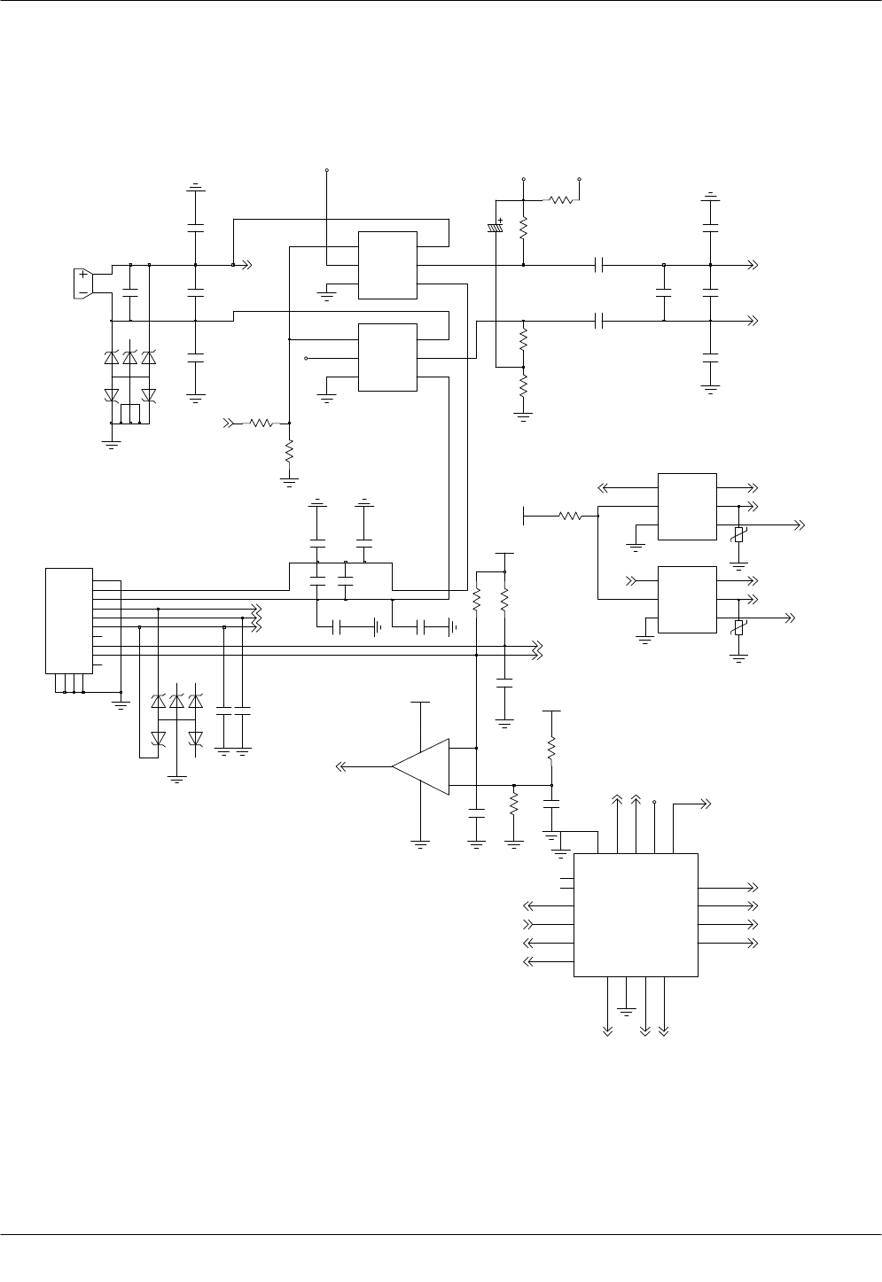
12. GSMReceiver
U100 Pin7
>= -65dBmResolderRFS100,C102
END
No
Yes
RXON
RFinput:CHcenterfreq: +67.7kHz
Amp:-50dBm
CheckU100
pin2,pin4,pin8=L
U100 pin5
>= -65dBm
F100 pin1
>= -67dBm
U102 pin7,8,9,10
>= 1V
U102
pin29 >= -70dBm
pin30 >= -70dBm
CheckANTSwitch
controlcircuit
ResolderU100
ResolderF100,C104,L102
ResolderC103,C105,L101
CheckU102
pin23,26,31 >=2.7VCheck&Resolder
U102,R103,R104
RF26MHz,RFPSUPart
ResolderU102
R112,R113,R114,
R115 >= 1V
Yes
Yes
Yes
Yes
Yes
Yes
Yes
Yes
No
No
No
NoNo
No
CheckU200
SAMSUNG Proprietary-Contents may change without notice
ThisDocumentcan notbe used withoutSamsung'sauthorization
FlowChartofTroubleshooting
7-24
13. GSMTransmitter
U100 Pin7
>= 20dBmResolderRFS100,C102,L106
TXON(5Level)
CheckU100
pin4=H(2.68V),
pin2,8=L
U100 pin10
>= 18dBm
PAM100 pin16
>= 18dBm
OSC100 pin1
>= -15dBm
PAM100 pin5
>= -11dBm
ChangeorResolderU100
CheckANTSwitch
controlcircuit
ResolderC134,L108,C149
ResolderR114,R116,R117
U102 pin6,7,8,9
>= 1V
Yes
CheckPAM100
+VBAT,
pin2,3,13,14 OK?ResolderorChangePAM100
Check+VBATorPAM
controlsignal
Check&ResolderRFLO
signal, RF13MHz,
RFPSUPart
Yes
Yes
Yes
Yes
Yes
Yes
Yes
Yes
No
No
No
No
No
No
No
No
No
END
CheckU205
ResolderU102
Yes
CheckU102
pin23,26,31
>=2.7V

SAMSUNG Proprietary-Contents may change without notice
FlowChartofTroubleshooting
ThisDocumentcan notbe used withoutSamsung'sauthorization
7-25
14. DCSReceiver
U100 Pin7
>= -65dBmResolderRFS100,C102,L602
No
Yes
RXON
RFinput:CHcenterfreq: +67.7kHz
Amp:-50dBm
CheckU100
pin2,pin4,pin8=L
U100 pin1
>= -65dBm
F102 pin1
>= -67dBm
U102 pin7,8,9,10
>= 1V
U102
pin35 >= -70dBm
pin36 >= -70dBm
CheckANTSwitch
controlcircuit
ResolderU100
ResolderF102,C121,L107
ResolderC120,C122,L106
CheckU102
pin23,26,31 >=
2.7V
Check&Resolder
U102,R103,R104
RF26MHz,RFPSUPart
ResolderU102
R112,R113,R114,
R115 >= 1V
Yes
Yes
Yes
Yes
Yes
Yes
Yes
Yes
No
No
No
NoNo
No
END
CheckU200

SAMSUNG Proprietary-Contents may change without notice
ThisDocumentcan notbe used withoutSamsung'sauthorization
FlowChartofTroubleshooting
7-26
15. DCSTransmitter
U100 Pin7
>= 20dBmResolderRFS100,C102,L106
TXON(5Level)
CheckU100
pin2,pin4=L,
pin8=H
U100 pin9
>=18dBm
PAM100 pin18
>= 18dBm
U102 pin2
>= -15dBm
PAM100 pin5
>= -11dBm
ChangeorResolderU100
CheckANTSwitch
controlcircuit
ResolderL115,C135
ResolderR116,R117,R118,C147,L117,C138,C132
U102 pin7,8,9,10
>= 1V
Yes
CheckPAM100
+VBAT,
pin2,3,13,14 OK?ResolderorChangePAM100
Check+VBATorPAM
controlsignal
CheckU102
pin23,26,31
>= 2.7V
Check&ResolderRFLO
signal, RF26MHz,
RFPSUPart
Yes
Yes
Yes
Yes
Yes
Yes
Yes
Yes
No
No
No
No
No
No
No
No
No
END
CheckU200
ResolderU102
Yes

SAMSUNG Proprietary-Contents may change without notice
FlowChartofTroubleshooting
ThisDocumentcan notbe used withoutSamsung'sauthorization
7-27
16. PCSReceiver
U100 Pin7
>= -65dBmResolderRFS100,C102,L602
No
Yes
RXON
RFinput:CHcenterfreq: +67.7kHz
Amp:-50dBm
CheckU100
pin2=H,
pin4,pin8=L
U100 pin3
>= -65dBm
F101 pin1
>= -67dBm
U102 pin7,8,9,10
>= 1V
U102
pin32 >= -70dBm
pin33 >= -70dBm
CheckANTSwitch
controlcircuit
ResolderU100
ResolderF101,C115,L105
ResolderC112,C119,L104
CheckU102
pin23,26,31 >=
2.7V
Check&Resolder
U102,R103,R104
RF26MHz,RFPSUPart
ResolderU102
R112,R113,R114,
R115 >= 1V
Yes
Yes
Yes
Yes
Yes
Yes
Yes
Yes
No
No
No
NoNo
No
END
CheckU200
SAMSUNG Proprietary-Contents may change without notice
ThisDocumentcan notbe used withoutSamsung'sauthorization
FlowChartofTroubleshooting
7-28
17. PCSTransmitter
U100 Pin7
>= 20dBmResolderRFS100,C102,L106
TXON(5Level)
CheckU100
pin2,pin8=H,
pin4=L
U100 pin9
>=18dBm
PAM100 pin18
>= 18dBm
U102 pin2
>= -15dBm
PAM100 pin5
>= -11dBm
ChangeorResolderU100
CheckANTSwitch
controlcircuit
ResolderL115,C135
ResolderR116,R117,R118,C147,L117,C138,C132
U102 pin7,8,9,10
>= 1V
Yes
CheckPAM100
+VBAT,
pin2,3,13,14 OK?ResolderorChangePAM100
Check+VBATorPAM
controlsignal
CheckU102
pin23,26,31
>= 2.7V
Check&ResolderRFLO
signal, RF26MHz,
RFPSUPart
Yes
Yes
Yes
Yes
Yes
Yes
Yes
Yes
No
No
No
No
No
No
No
No
No
END
CheckU200
ResolderU102
Yes
SAMSUNG Proprietary-Contents may change without notice
FlowChartofTroubleshooting
ThisDocumentcan notbe used withoutSamsung'sauthorization
7-29
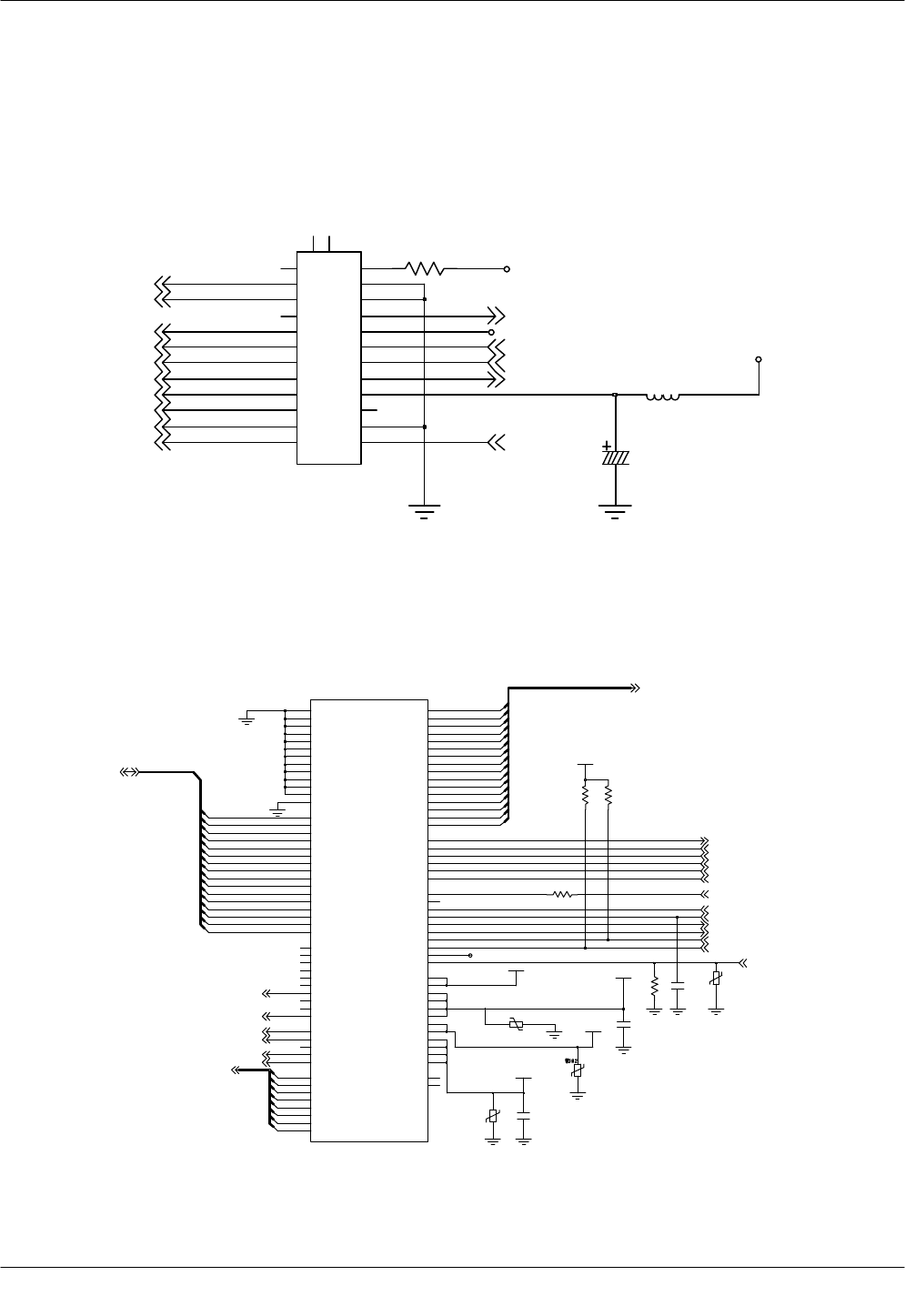
GSM900 RX
DCS RX
PCS RX
C137
39PF
C114
100PF
33PF
C119
7P F
R112
0
C109
100NF
C118
+VCC_SYN
33
SWON
40
TXVCC
39
26
VCCCP
VCCI F
11
31
VCCRF
28
VCCRFL
O
23
VCCSYN
16
VDDL
LBO
38
NC1
45
46
NC2
17
PGMDI V
10 QA
9 QB
21
REFIN
19
REFVCC
RFTUNE
25
SWBI A
32
SWBI B
34
GNDRF3
1
3 GNDRF4
GNFRF2
37
HBIA
35
HBIB
36
2 HB
O
IA
8
IB
7
29
LBIA
LBIB 30
EN
EXTRES
27
4 FESW
1
FESW
2
5
FESW
3
6
GND1
41
42
GND2
GND3
43
44
GND4
GNDL
15
GNDREF
22
GNDRF1
UAA3587GHN
U102
CLK
13
CLKFDBX
20
CLKOUT
18
CTRL 24
DATA
12 14
330
R108
R103
10
100PF
C113
C129 100PF
C121
33PF
C150
NC
39PF
C111
L109
C110
100NF
6.2nH
L106
8.2PF
5
1 IN OUT 3
OU T 4
L107
F100
FAR-F5EB-942M50-B28EH
2
GG
12nH
12nH
R115
0
L105
NC
C136
C112
33PF
220NF
C123
R104
220K
+VCC_SYN
100PF
C151
R114
0
C145
NC
L118
100nH
C115
C104 39PF
39PF
R113
0
10K
R101
F101
FAR-F6EB-1G9600-B2BE
2
GG
5
IN
1
3
OUT
OUT 4
C120
+VCC_SYN
18PF 220K
R102
C117
100NF
L101
18nH
5.6nH
47PF
C103
L104
NC
C146
18
R106
R107
330
39PF 10N F
C141 C140
L102
1.0nH
L100
22nH
NC
C101 C100
NC
0
R100
L103
33nH
C105
47PF
C122
18PF
27PF
C133
2
GND
3 OU T
VC C
4
VCON
1
2
GG
5
IN
1
3
OUT
OUT
4
U101
TCO-5871U 26MHz
F102
FAR-F6EB-1G8425-B2BG
FESW 2
GSM_TX
+VDD_RX_TX
26M_CLK
AFC
PON_3587_SYNTH
+VDD_RX_TX
PON_SW
RF_DATA
RF_CLK
RF_EN
+VDD_IO_LO W
D_REF_CLK
DCS_TX
FESW 3
FESW 1 RX_TX_I P
RX_TX_I N
RX_TX_Q
P
RX_TX_Q
N
+VCC_SYN
SAMSUNG Proprietary-Contents may change without notice
PCB Diagrams
6-4
ThisDocumentcan notbe used withoutSamsung'sauthorization
4.Sub PCB BottomDiagram
