ShangHai Ehong Technology MB18 Bluetooth Module User Manual Datasheet
ShangHai Ehong Technology Co.,Ltd. Bluetooth Module Datasheet
15_EH-MB18 UserMan.pdf
Ehong Technology Co., Ltd
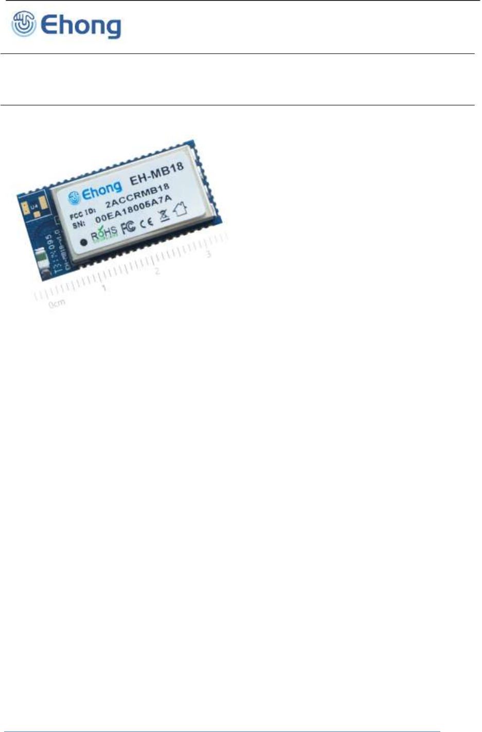
EH-MB18
Bluetooth® Technology Audio
Module
•
Bluetooth radio
- Fully embedded Bluetooth® v4.2(Smart ready)
- Bluetooth® v3.0 specification compliant
- TX power +8dbm,-90dbm RX sensitivity
- 128-bit encryption security
- Range up to 15m
- Internal chip antenna or U.fl port
- Multipoint capability(7 transmit data devices
connected at the same time)
•
Support profiles
- SPP (Master and slave), iAP (ipod accessory
protocol)
- BLE(GATT Profile)
- HFP ,A2DP,AVRCP,HID(Salve)
•
User interface
- Send AT command over UART
- Firmware upgrade over USB
- With SPP service active: 560kbps transmission
speed (UART)
- PCM interface (I2S,SPDIF)
- I2C interface(Master ),SPI
•
Audio codec
- optional support for 64Mb of external SPI flash
16Mb internal flash memory (64-bit wide, 45ns)
- 80MHz RISC MCU and 80MIPS Kalimba DSP
- Support for CSR's latest CVC technology for
narrow-band and wideband voice connections
including wind noise reduction
- Support Apt-X ,AAC, Apt-XLL,SBC codec
•
General
I/O
-
13 eneral purpose I/Os
-
2 analogue I/O
-
Support for up to 3 capacitive touch sensor
inputs
-
Three fully configurable LED drivers
•
FCC and Bluetooth® qualified
•
Single voltage supply: 2.7-3.6V
•
Small form factor: 30.4 x 15.26 x 2.4mm
•
Operating temperature range: -40 °C to 85 °C

Bluetooth Audio Module
Ehong Technology Co., Ltd
1. Contents
1. Description ......................................................................................................................................................... 4
2. Application ......................................................................................................................................................... 4
3. EH-MB18 Product numbering ........................................................................................................................ 4
4. Electrical Characteristic .................................................................................................................................. 5
4.1. Recommend operation conditions ............................................................................................................ 5
4.2. Absolute Maximum Rating ......................................................................................................................... 5
4.3. Power consumptions .................................................................................................................................. 5
4.4. Input/output Terminal Characteristics ...................................................................................................... 7
4.4.1. Digital Terminals .................................................................................................................................. 7
4.4.2. USB ....................................................................................................................................................... 8
4.4.3. Internal CODEC Analogue to Digital Converter .............................................................................. 8
4.4.4. Internal CODEC Digital to Analogue Converter.............................................................................. 9
5. Pinout and Terminal Description ................................................................................................................ 10
5.1. Pin assignment .......................................................................................................................................... 10
6. Physical Interfaces ......................................................................................................................................... 13
6.1. Power Supply ............................................................................................................................................. 13
6.2. Reset ........................................................................................................................................................... 13
6.3. PIO .............................................................................................................................................................. 14
6.4. AIO .............................................................................................................................................................. 14
6.5. RF interface ............................................................................................................................................... 14
6.6. UART .......................................................................................................................................................... 14
6.7. I2C Master .................................................................................................................................................. 15
6.8. Apple iOS CP reference design .............................................................................................................. 16
6.9. Digital Audio Interfaces ............................................................................................................................ 17
6.9.1. PCM .................................................................................................................................................... 18
6.9.2. Digital Audio Interface (I2S) ............................................................................................................. 19
6.9.3. IEC 60958 Interface (SPDIF) .......................................................................................................... 22
6.10. Microphone input ................................................................................................................................... 23
6.11. Analog Output stage ............................................................................................................................. 24
6.12. USB ......................................................................................................................................................... 24
7. EH-MB18 Reference Design ......................................................................................................................... 26

Bluetooth Audio Module
Ehong Technology Co., Ltd
8. Mechanical and PCB Footprint Characteristics ...................................................................................... 27
9. RF Layout Guidelines .................................................................................................................................... 28
10. Reflow Profile ............................................................................................................................................... 29
11. Contact Information ................................................................................................................................... 30
2. Table of Tables
TABLE 1: RECOMMENDED OPERATING CONDITIONS .................................................................................................... 5
TABLE 2: ABSOLUTE MAXIMUM RATING RECOMMENDED OPERATING CONDITIONS ................................................... 5
TABLE 3: POWER CONSUMPTIONS ................................................................................................................................ 7
TABLE 4: DIGITAL TERMINAL ......................................................................................................................................... 8
TABLE 5: USB TERMINAL .............................................................................................................................................. 8
TABLE 6: ANALOGUE TO DIGITAL CONVERTER ............................................................................................................. 9
TABLE 7: DIGITAL TO ANALOGUE CONVERTER ........................................................................................................... 10
TABLE 8:PIN TERMINAL DESCRIPTION ..................................................................................................................... 13
TABLE 9: PIN STATUS ON RESET ................................................................................................................................ 14
TABLE 10: POSSIBLE UART SETTINGS ...................................................................................................................... 15
TABLE 11: ALTERNATIVE FUNCTIONS OF THE DIGITAL AUDIO BUS INTERFACE ON THE PCM INTERFACE ............... 18
TABLE 12 : DIGITAL AUDIO INTERFACE SLAVE TIMING ............................................................................................... 21
TABLE 13 : DIGITAL AUDIO INTERFACE MASTER TIMING............................................................................................ 21
TABLE 14: USB INTERFACE COMPONENT VALUES .................................................................................................... 25
3. Table of Figures
FIGURE 1:PINOUT OF EH-MB18.............................................................................................................................. 10
FIGURE 2:POWER SUPPLY PCB DESIGN ................................................................................................................ 13
FIGURE 3:CONNECTION TO HOST DEVICE ............................................................................................................... 15
FIGURE 4 : EXAMPLE EEPROM CONNECTION WITH I2C INTERFACE ........................................................................ 16
FIGURE 5 : APPLE CO-PROCESSOR 2.0C ................................................................................................................... 16
FIGURE 6 : APPLE CO-PROCESSOR 2.0B ................................................................................................................... 17
FIGURE 7 : AUDIO INTERFACE ..................................................................................................................................... 18
FIGURE 8 : DIGITAL AUDIO INTERFACE MODES .......................................................................................................... 20
FIGURE 9 : DIGITAL AUDIO INTERFACE SLAVE TIMING ............................................................................................... 21
FIGURE 10 : DIGITAL AUDIO INTERFACE MASTER TIMING .......................................................................................... 21
FIGURE 11: EXAMPLE CIRCUIT FOR SPDIF INTERFACE (CO-AXIAL) ........................................................................ 22
FIGURE 12: EXAMPLE CIRCUIT FOR SPDIF INTERFACE (OPTICAL) ........................................................................... 22
FIGURE 13: MICROPHONE BIASING (SINGLE CHANNEL
S
HOWN
)
............................................................................... 23
FIGURE 14: SPEAKER OUTPUT .................................................................................................................................... 24
FIGURE 15: USB CONNECTIONS ................................................................................................................................ 25
FIGURE 16: REFERENCE DESIGN ............................................................................................................................... 26
FIGURE 17: RECOMMENDED PCB MOUNTING PATTERN (UNIT: MM, DEVIATION:0.02MM)TOP VIEW ..................... 27
FIGURE 18: CLEARANCE AREA OF ANTENNA ............................................................................................................. 28
FIGURE 19: RECOMMENDED REFLOW PROFILE ......................................................................................................... 29

Bluetooth Audio Module
Ehong Technology Co., Ltd
1. Description
The EH-MB18 is an easy to use Bluetooth module, compliant with Bluetooth v4.2. The module
provides complete RF platform in a small form factor.
The module enables electronic devices with wireless connectivity, not requiring any RF
experience or expertise for integration into the final product. The module being a certified
solution optimizes the time to market of the final application.
The module built-in enhanced Kalimba DSP coprocessor with 80MIPS, supports enhanced
audio and DSP Applications (t Apt-X, AAC, Apt-XLL, SBC codec).Support GATT,A2DP, AVRCP,
HSP, HFP,SPP, iAP and PBAP Profiles communication with smart ready devices.
The module BLE profile communication with smart phones (iOS and Android), must be install
the APP. EHong iOS system APP download address: https://itunes.apple.com/cn/app/ehong-
link/id854886208?mt=8.
The module has 14 x general purpose IOs, 2x Analogue inputs/outputs (temperature sensor,
charger control, etc), 3xs capacitive touch sensors, three fully configurable LED drivers
(PWM).The module optional support for 64Mb of external SPI flash 16Mb internal flash memory
(64-bit wide, 45ns),support Li-Ion battery charger with Instant-ON.
2. Application
Home entertainment eco-system
TVs
Smart remote controllers
Wired or wireless sound bars
Wired or wireless speakers and headphones
Bluetooth low energy connectivity to external 3D glasses
Tablets / PCs / Mobile Connectivity
Wired or wireless headphones for music / gaming / multimedia content
Wired or wireless speakers
Wired or wireless speaker phones
Mono Headsets for voice
3. EH-MB18 Product numbering
EH-MB18(B)
A. EH ------------- Company Name(Ehong)
B. MB18 ------------ Module Name
C. B ------------- U.FL Connector
Bluetooth Audio Module
Ehong Technology Co., Ltd
4. Electrical Characteristic
4.1. Recommend operation conditions
Operating Condition
Min
Typical
Max
Unit
Operating Temperature Range
-40
--
+85
°C
PIO Voltage
+1.7
+3.3
+3.6
V
AIO Voltage
+1.7
+1.8
+1.95
V
LED
+1.1
3.7
+3.6
V
VDD Voltage
+2.7
+3.3
+3.6
V
VCHG(a)
+4.75
+5
+5.75
V
RF frequency
2400
2441
24800
MHz
Table 1: Recommended Operating Conditions
Note:(a) Maximum charging current 200mA
4.2. Absolute Maximum Rating
Table 2: Absolute Maximum Rating Recommended Operating Conditions
4.3. Power consumptions
DUT Role
Connection
Packet Type
Average
Current
Unit
N/A
Deep
sleep
With UART host
connection
-
55
uA
N/A
Page
scan
Page = 1280ms
interval
Window = 11.25ms
-
219
uA
Rating Min Max Unit
Storage Temperature -40 +125 °C
PIO Voltage -0.4 +3.6 V
AIO Voltage -0.4 +1.95 V
LED -0.4 +3.6 V
VDD Voltage -0.4 +3.6 V
VCHG -0.4 +5.75 V
USB_DP/USB_DN Voltage -0.4 +3.6 V
Other Terminal Voltages VSS-0.4 VDD+0.
4 V

Bluetooth Audio Module
Ehong Technology Co., Ltd
N/A
Inquiry
a n d
p a g e
sca n
Inquiry
=
1280m
s
interval
Page =
1280m
s
interval
W ind o
w =
11.25m
s
-
378
uA
Master
ACL
Sniff = 500ms, 1
attempt, 0 timeout
DH1
119
uA
Master
ACL
Sniff = 1280ms, 8
attempts, 1 timeout
DH1
109
uA
Master
SCO
Sniff = 100ms, 1
attempt, PCM
HV3
7.6
mA
Master
SCO
Sniff = 100ms, 1
attempt, mono audio
codec
HV3
9.8
mA
Master
eSCO
Setting S3, sniff =
100ms, PCM
2EV3
5.8
mA
Master
eSCO
Setting S3, sniff =
100ms, PCM
3EV3
5.4
mA
Master
eSCO
Setting S3, sniff =
100ms, mono audio
codec
2EV3
7.9
mA
Master
eSCO
Setting S3, sniff =
100ms, mono audio
codec
3EV3
7.5
mA
Slave
ACL
Sniff = 500ms, 1
attempt, 0 timeout
DH1
127
uA
Slave
ACL
Sniff = 1280ms, 8
attempts, 1 timeout
DH1
129
uA
Slave
SCO
Sniff = 100ms, 1
attempt, PCM
HV3
7.8
mA
Slave
SCO
Sniff = 100ms, 1
attempt, mono audio
codec
HV3
10
mA
Slave
eSCO
Setting S3, sniff =
100ms, PCM
2EV3
6.2
mA
Slave
eSCO
Setting S3, sniff =
3EV3
5.8
mA
Bluetooth Audio Module
Ehong Technology Co., Ltd
100ms, PCM
Slave
eSCO
Setting S3, sniff =
100ms, mono audio
codec
2EV3
8.2
mA
Slave
eSCO
Setting S3, sniff =
100ms, mono audio
codec
3EV3
7.9
mA
Table 3: Power consumptions
Note : Current consumption values are taken with:
■ Firmware ID = 7919
■ RF TX power set to 0dBm
■ No RF retransmissions in case of eSCO
■ Audio gateway transmits silence when SCO/eSCO channel is open
■ LEDs disconnected
■ AFH off
4.4. Input/output Terminal Characteristics
4.4.1. Digital Terminals
Digital Terminals
Min
Type
Max
Unit
Input Voltage
VIL input logic level low
-
0.4
-
0.4
V
VIH input logic level high
0.7 x VDD
-
VDD + 0.4
V
Tr/Tf
-
-
25
ns
Output Voltage
VOL output logic level low, lOL = 4.0mA
-
-
0.4
V
VOH output logic level high, lOH = -4.0mA
0.75 X
VDD
-
-
V
Tr/Tf
-
-
5
ns
Input and Tristate Currents
Strong pull-up
-150
-40
-10
μA
Strong pull-down
10
40
150
μA
Weak pull-up
-5
-1.0
-0.33
μA
Weak pull-down
0.33
1.0
5.0
μA
CI Input Capacitance
1.0
-
5.0
pF
Bluetooth Audio Module
Ehong Technology Co., Ltd
Table 4: Digital Terminal
4.4.2. USB
Min
Type
Max
Unit
VDD_USB for correct USB operation
3.10
3.30
3.60
V
Input Threshold
VIL input logic level low
-
-
0.30
x
VDD_US
B
V
VIH input logic level high
0.70
x
VDD_US
B
-
-
V
Input Leakage Current
VSS_DIG < VIN < VDD_USB(a)
-1
1
5
µA
CI input capacitance
2.5
-
10
pF
Output Voltage Levels to Correctly Terminated USB Cable
VOL output logic level low
0
-
0.2
V
VOH output logic level high
2.80
-
VDD_USB
V
Table 5: USB Terminal
(a) Internal USB pull-up disable
4.4.3. Internal CODEC Analogue to Digital Converter
Analogue to Digital Converter
Parameter
Conditions
Min
Type
Max
Unit
Resolution
-
-
-
16
Bits
Input Sample
Rate, Fsample
-
8
-
48
kHz
fin = 1kHz
B/W =
20Hz→Fsample/
Fsample
8kHz
-
93
-
dB
16kHz
-
92
-
dB
Bluetooth Audio Module
Ehong Technology Co., Ltd
SNR
2 (20kHz max)
A-Weighted
THD+N < 0.1%
1.6Vpk-pk input
32kHz
-
92
-
dB
44.1kHz
-
92
-
dB
48kHz
-
92
-
dB
THD+N
fin = 1kHz
B/W =
20Hz→Fsample/
2 (20kHz max)
1.6Vpk-pk input
Fsample
8kHz
-
0.004
-
%
48kHz
-
0.008
-
%
Digital gain
Digital gain resolution = 1/32
-24
-
21.5
dB
Analogue gain
Pre-amplifier setting = 0dB,
9dB, 21dB or
30dB
Analogue setting = -3dB to
12dB in 3dB
steps
-
3
-
42
dB
Stereo separation (crosstalk)
-
-89
-
dB
Table 6: Analogue to Digital Converter
4.4.4. Internal CODEC Digital to Analogue Converter
Digital to Analogue Converter
Parameter
Conditions
Min
Type
Max
Unit
Resolution
-
-
-
16
Bit
s
Output Sample
Rate, Fsample
-
8
-
96
kHz
SNR
fin = 1kHz
B/W =
20Hz→20kHz
A-Weighted
THD+N < 0.01%
0dBFS input
Fsample
Load
48kHz
100kΩ
-
96
-
dB
48kHz
32Ω
-
96
-
dB
48kHz
16Ω
-
96
-
dB
THD+N
fin = 1kHz
B/W =
20Hz→20kHz
0dBFS input
Fsample
Load
8kHz
100kΩ
-
0.002
-
%
8kHz
32Ω
-
0.002
-
%
8kHz
16Ω
-
0.003
-
%
48kHz
100kΩ
-
0.003
-
%
48kHz
32Ω
-
0.003
-
%
Bluetooth Audio Module
Ehong Technology Co., Ltd
48kHz
16Ω
-
0.004
-
%
Digital Gain
Digital Gain Resolution = 1/32
-24
-
21.5
dB
Analogue Gain
Analogue Gain Resolution = 3dB
-21
-
0
dB
Stereo separation (crosstalk)
-
-88
-
dB
Table 7: Digital to Analogue Converter
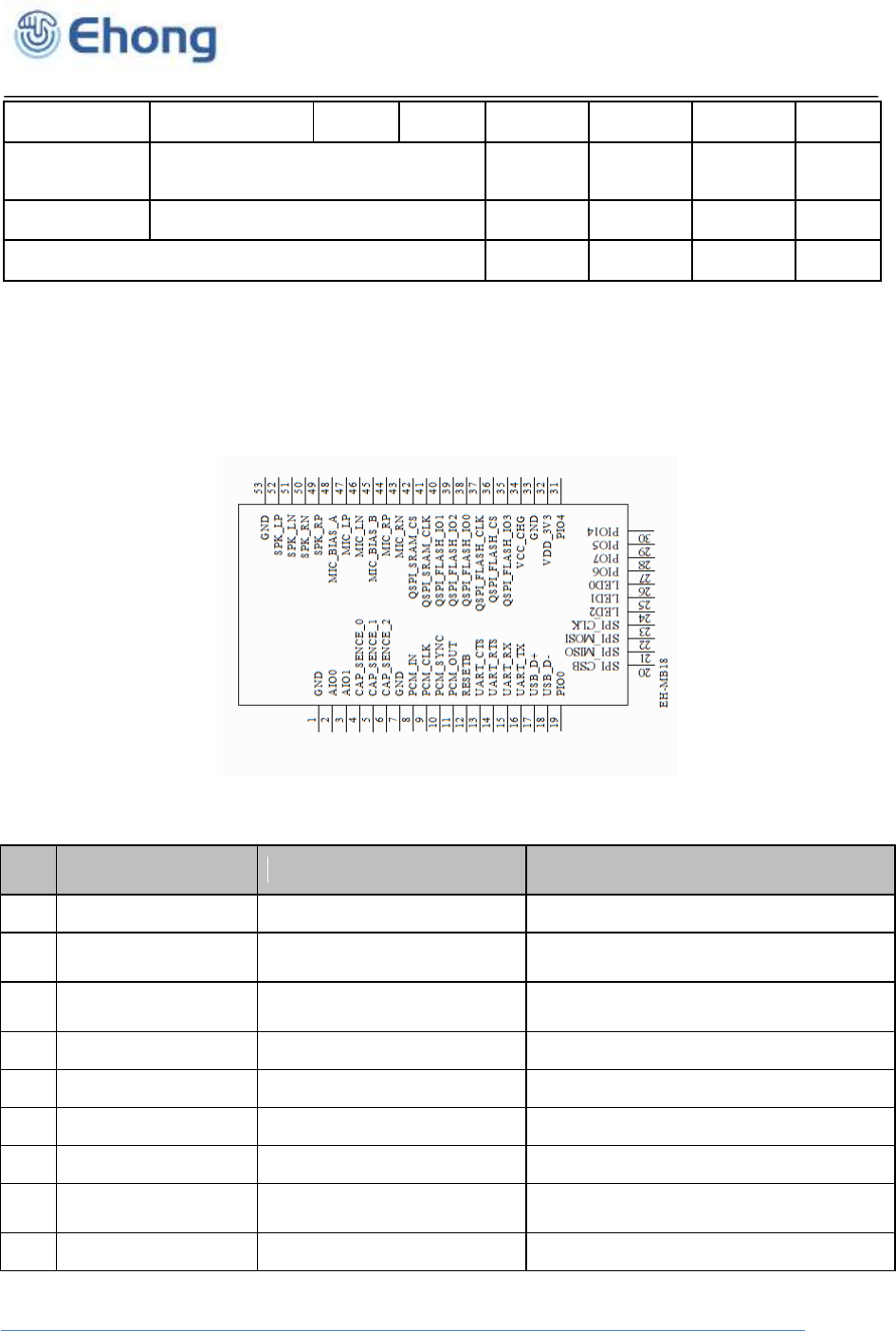
5. Pinout and Terminal Description
5.1. Pin assignment
Figure 1:Pinout of EH-MB18
Pin
Symbol
I/O Type
Description
1
GND
Ground
Ground
2
AIO0
Bi-directional
Analogue programmable input/output
line
3
AIO1
Bi-directional
Analogue programmable input/output
line
4
CAP_SENSE0
Analogue input
Capacitive touch sensor input
5
CAP_SENSE1
Analogue input
Capacitive touch sensor input
6
CAP_SENSE2
Analogue input
Capacitive touch sensor input
7
GND
Ground
Ground
8
PCM_IN
CMOS Input, with weak
internal pull-down
Synchronous Data Input
9
PCM_CLK
Bi-directional with weak
Synchronous Data Clock

Bluetooth Audio Module
Ehong Technology Co., Ltd
internal pull-down
10
PCM_SYNC
Bi-directional with weak
internal pull-down
Synchronous Data Sync
11
PCM_OUT
CMOS output, tri-state,
with weak internal pull-
down
Synchronous Data Output
12
RESETB
CMOS input with weak
internal pull-up
Active LOW RESETB, input
debounced so must be low for >5ms
to cause a RESETB
13
UART_CTS
Bi-directional with weak
pull down
Uart clear to send ,active low
14
UART_RTS
Bi-directional with weak
internal pull-up
uart request to send ,active low
15
UART_RX
CMOS input with weak
internal pull-down
UART data input
16
UART_TX
Bi-directional CMOS
output, tri-state, with weak
internal pull-up
UART data output
17
USB_D+
Bi-directional
USB data plus with selectable
internal 1.5K pull up resistor
18
USB_D-
Bi-directional
USB data minus
19
PIO0
Bi-directional with
programmable strength
internal pull-up/down
Programmable input/output line
20
SPI_CSB
Input with weak internal
pull-up
Chip select for Synchronous Serial
Interface for programming only,
active low
21
SPI_MISO
CMOS output, tri-state,
with weak internal pull-
down
Serial Peripheral Interface output for
programming only
22
SPI_MOSI
CMOS input, with weak
internal pull-down
Serial Peripheral Interface input for
programming only
23
SPI_CLK
Input with weak internal
pull-down
Serial Peripheral interface clock for
programming only
24
LED2
Open drain output
LED Driver
25
LED1
Open drain output
LED Driver
26
LED0
Open drain output
LED Driver
27
PIO6
Bi-directional with
programmable strength
internal pull-up/down
Programmable input/output line
28
PIO7
Bi-directional with
programmable strength
Programmable input/output line or
I2C SDA

Bluetooth Audio Module
Ehong Technology Co., Ltd
internal pull-up/down
29
PIO5
Bi-directional with
programmable strength
internal pull-up/down
Programmable input/output line or
I2C SCL
30
PIO14
Bi-directional with
programmable strength
internal pull-up/down
Programmable input/output line
31
PIO4
Bi-directional with
programmable strength
internal pull-up/down
Programmable input/output line
32
VDD_3V3
Power Supply
+2.7V- +3.6V power input
33
GND
Ground
Ground
34
VDD_CHG
Charger input
+4.7V--+5.7V charge input
35
QSPI_FALSH_IO3
Bi-directional with strong
internal pull-down
Serial quad I/O flash data bit 3
36
QSPI_FLASH_CS
Bi-directional with strong
internal pull-up
SPI flash chip select
37
QSPI_FLASH_CLK
Bi-directional with strong
internal pull-down
SPI flash clock
38
QSPI_FLASH_IO0
Bi-directional with strong
internal pull-down
Serial quad I/O flash data bit 0
39
QSPI_FLASH_IO2
Bi-directional with strong
internal pull-down
Serial quad I/O flash data bit 2
40
QSPI_FLASH_IO1
Bi-directional with strong
internal pull-down
Serial quad I/O flash data bit 1
41
QSPI_SRAM_CLK
Bi-directional with strong
internal pull-down
SPI RAM clock
42
QSPI_SRAM_CS
Bi-directional with strong
internal pull-up
SPI RAM chip select
43
MIC_RN
Analogue
Microphone input negative, right
44
MIC_RP
Analogue
Microphone input positive, right
45
MIC_BIAS_B
Analogue out
Microphone bias B
46
MIC_LN
Analogue
Microphone input negative, right
47
MIC_LP
Analogue
Microphone input positive, left
48
MIC_BIAS_A
Analogue out
Microphone bias A
49
SPK_RP
Analogue
Speaker output positive, right
50
SPK_RN
Analogue
Speaker output negative, right
51
SPK_LN
Analogue
Speaker output negative, left
Bluetooth Audio Module
Ehong Technology Co., Ltd
52
SPK_LP
Analogue
Speaker output positive, left
53
GND
Ground
Ground
Table 8:PIN Terminal Description
6. Physical Interfaces
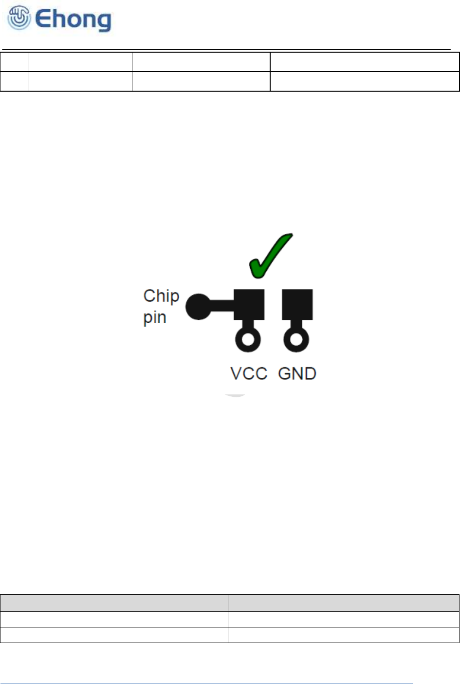
6.1. Power Supply
- The module DC3.3V power input.
- Power supply pin connection capacitor to chip and pin as far as possible close
- Capacitor decouples power to the chip
- Capacitor prevents noise coupling back to power plane.
.
Figure 2:Power Supply PCB Design
6.2. Reset
The module may be reset from several sources: RESETB pin, power-on reset, a UART break
character or via software configured watchdog timer.
The RESETB pin is an active low RESETB and is internally filtered using the internal low
frequency clock oscillator. A RESETB will be performed between 1.5 and 4.0ms following
RESETB being active. It is recommended that RESETB be applied for a period greater than
5ms.
At RESETB the digital I/O pins are set to inputs for bi-directional pins and outputs are tri-state.
The pull-down state is shown below.
Pin Name / Group
Pin Status on RESETB
USB_DP
N/a
USB_DN
N/a
Bluetooth Audio Module
Ehong Technology Co., Ltd
UART_RX
Strong PU
UART_TX
Weak PU
UART_RTS
Weak PU
UART_CTS
Weak PD
SPI_MOSI
Weak PD
SPI_CLK
Weak PD
SPI_CSB
Strong PU
SPI_MISO
Weak PD
RESET
Strong PU
PIOs
Weak PD
PCM_IN
Weak PD
PCM_CLK
Weak PD
PCM_SYNC
Weak PD
PCM_OUT
Weak PD
QSPI_SRAM_CS
Strong PU
QSPI_FLASH_CS
Strong PU
QSPI_SRAM_CLK
Strong PD
QSPI_FLASH_CLK
Strong PD
Table 9: Pin Status on Reset
6.3. PIO
EH-MB18 has a total of 13digital programmable I/O terminals. They are powered from VDD .
Their functions depend on firmware running on the device. PIO lines can be configured through
software to have either weak or strong pull-ups or pull-downs.
Note:
All PIO lines are configured as inputs with weak pull-downs at reset.
Any of the PIO lines can be configured as interrupt request lines or as wake-up lines from sleep modes.
6.4. AIO
EH-MB18 has 2 analogue I/O terminals. Their functions depend on software. Typically ADC
functions can be configured to battery voltage measurement. They can also be used as a digital
PIO.
6.5. RF interface
EH-MB18 internet chip antenna and U.fl port choose one of the ways. U.fl port external antenna,
impedance is 50 ohm.
6.6. UART
This is a standard UART interface for communicating with other serial devices. The UART
interface provides a simple mechanism for communicating with other serial devices using the
RS232 protocol.
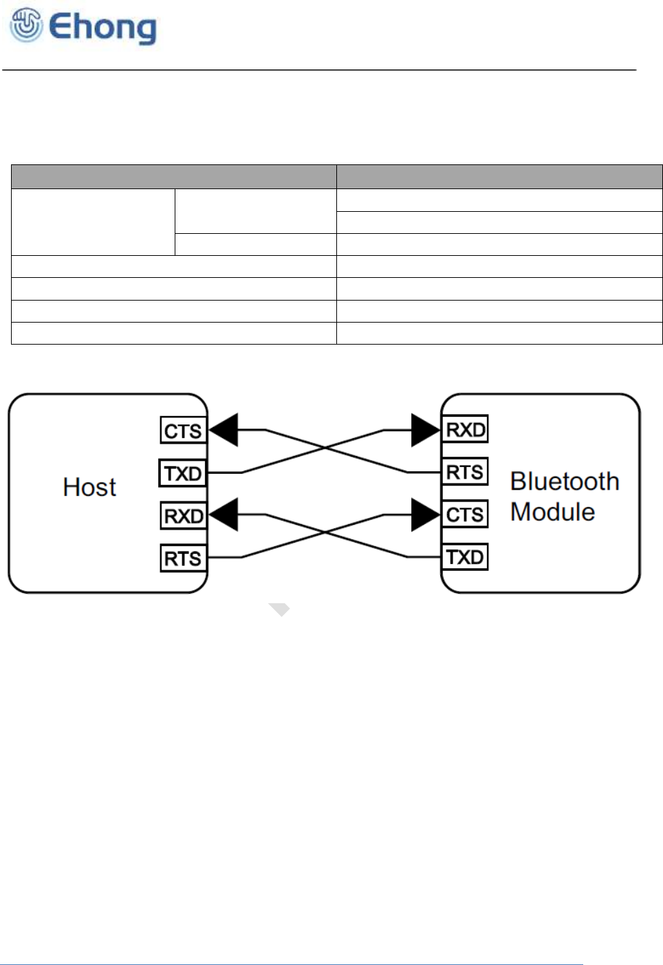
Bluetooth Audio Module
Ehong Technology Co., Ltd
The UART CTS and RTS signals can be used to implement RS232 hardware flow control where
both are active low indicators.
Table 10: Possible UART Settings
Figure 3:Connection To Host device
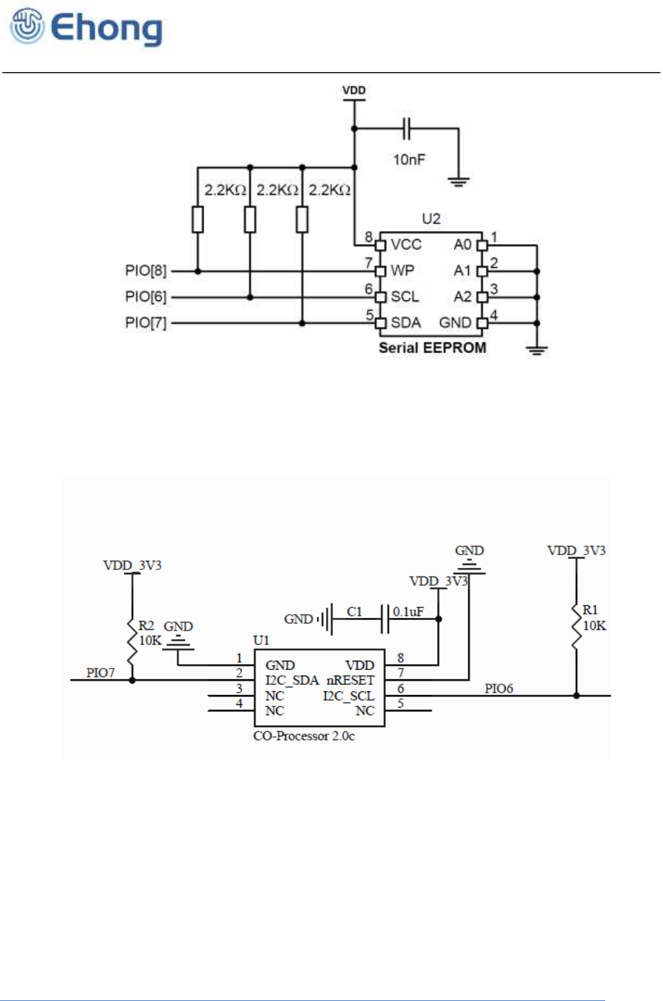
6.7. I2C Master
PIO6, PIO7 and PIO8 can be used to form a master I2C interface. The interface is formed using
software to drive these lines. It is suited only to relatively slow functions such as driving a LCD,
keyboard scanner or EEPROM. In the case, PIO lines need to be pulled up through 2.2KΩ
resistors.
Parameter Possible Values
Baud Rate Minimum 1200 baud (≤2%Error)
9600 baud (≤1%Error)
Maximum 3M baud (≤1%Error)
Flow Control RTS/CTS or None
Parity None, Odd or Even
Number of Stop Bits 1 or 2
Bits per Byte 8
Bluetooth Audio Module
Ehong Technology Co., Ltd
Figure 4 : Example EEPROM Connection with I2C Interface
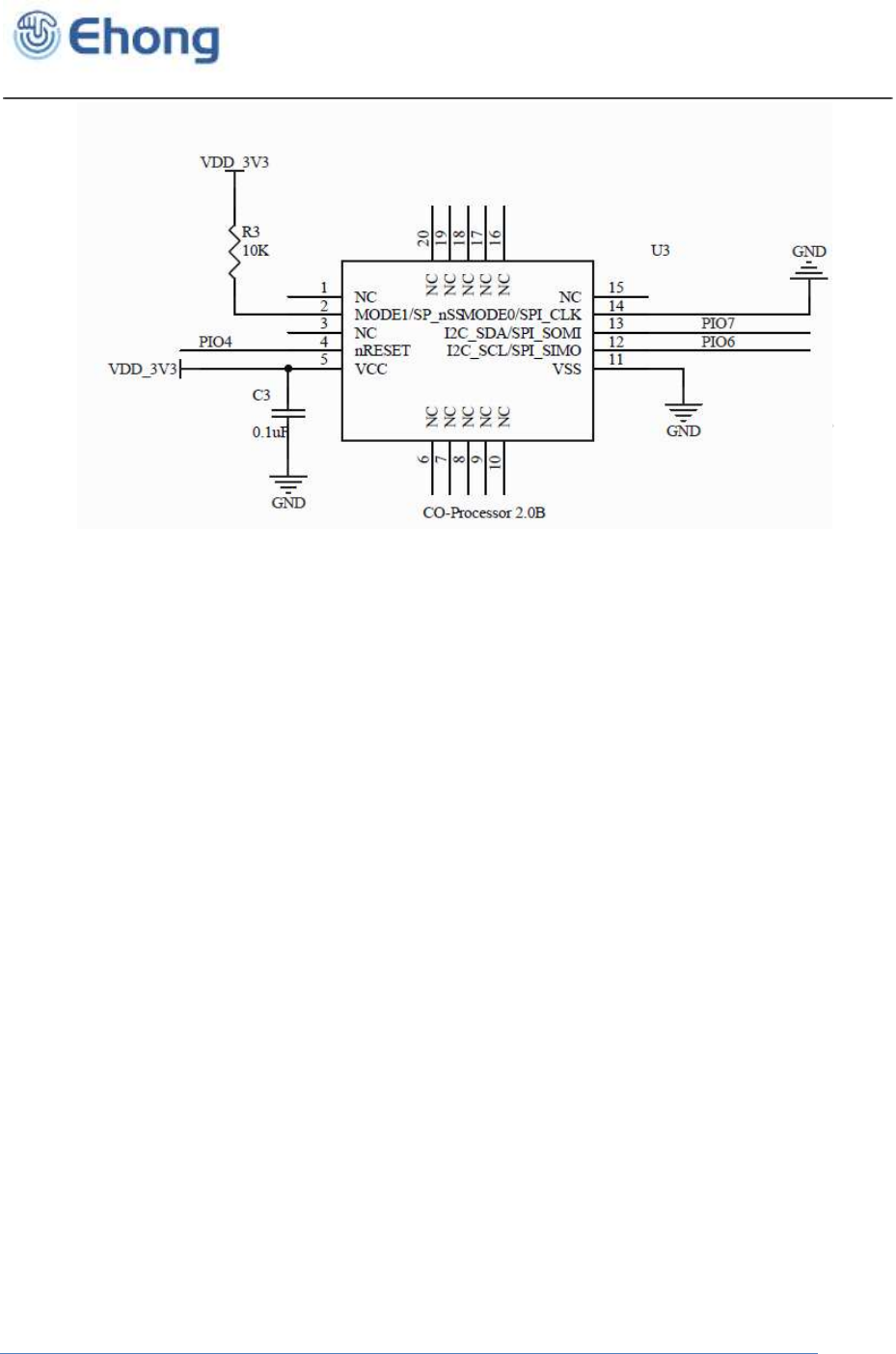
6.8. Apple iOS CP reference design
The figures below give an indicative overview of what the hardware concept looks like. A
specific MFI co-processor layout is available for licensed MFI developers from the MFI program.
Figure 5 : Apple Co-processor 2.0C
Bluetooth Audio Module
Ehong Technology Co., Ltd
Figure 6 : Apple Co-processor 2.0B
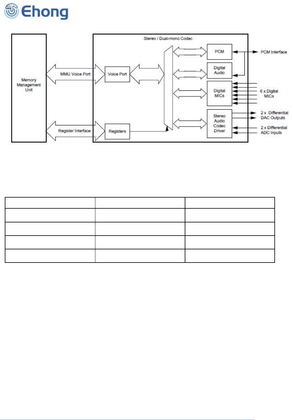
6.9. Digital Audio Interfaces
The audio interface circuit consists of:
■ Stereo/Dual-mono audio codec
■ Dual audio inputs and outputs
■ 6 digital MEMS microphone inputs
■ A configurable PCM, I²S or SPDIF interface
Figure 2 outlines the functional blocks of the interface. The codec supports stereo playback and
recording of audio signals at multiple sample rates with a resolution of 16-bit. The ADC and
the DAC of the codec each contain 2 independent channels. Any ADC or DAC channel can be
run at its own independent sample rate.
Bluetooth Audio Module
Ehong Technology Co., Ltd
Figure 7 : Audio Interface
The interface for the digital audio bus shares the same pins as the PCM codec interface
described in Table 11, which means each of the audio buses are mutually exclusive in their
usage. Table 11 lists these alternative functions.
PCM Interface
SPDIF Interface
I²S Interface
PCM_OUT
SPDIF_OUT
SD_OUT
PCM_IN
SPDIF_IN
SD_IN
PCM_SYNC
-
WS
PCM_CLK
-
SCK
Table 11: Alternative Functions of the Digital Audio Bus Interface on the PCM Interface
The audio input circuitry consists of a dual audio input that can be configured to be either
single-ended or fully differential and programmed for either microphone or line input. It has an
analogue and digital programmable gain stage for optimization of different microphones.
The audio output circuitry consists of a dual differential class A-B output stage.
6.9.1. PCM
The audio pulse code modulation (PCM) interface supports continuous transmission and
reception of PCM encoded audio data over Bluetooth.
Hardware on EH-MB18 allows the data to be sent to and received from a SCO connection. Up
to three SCO connections can be supported by the PCM interface at any one time.
EH-MB18 can operate as the PCM interface master generating PCM_SYNC and PCM_CLK or
as a PCM interface slave accepting externally generated PCM_SYNC and PCM_CLK.
EH-MB18 is compatible with a variety of clock formats, including Long Frame Sync, Short
Frame Sync and GCI timing environments.

Bluetooth Audio Module
Ehong Technology Co., Ltd
It supports 13-bit or 16-bit linear, 8-bit u-law or A-law companded sample formats and can
receive and transmit on any selection of three of the first four slots following PCM_SYNC.
EH-MB18 interfaces directly to PCM audio devices including the following:
■ Qualcomm MSM 3000 series and MSM 5000 series CDMA baseband devices
■ OKI MSM7705 four channel A-law and μ-law CODEC
■ Motorola MC145481 8-bit A-law and μ-law CODEC
■ Motorola MC145483 13-bit linear CODEC
■ STW 5093 and 5094 14-bit linear CODECs(8)
■ EH-MB18 is also compatible with the Motorola SSI interface
6.9.2. Digital Audio Interface (I2S)
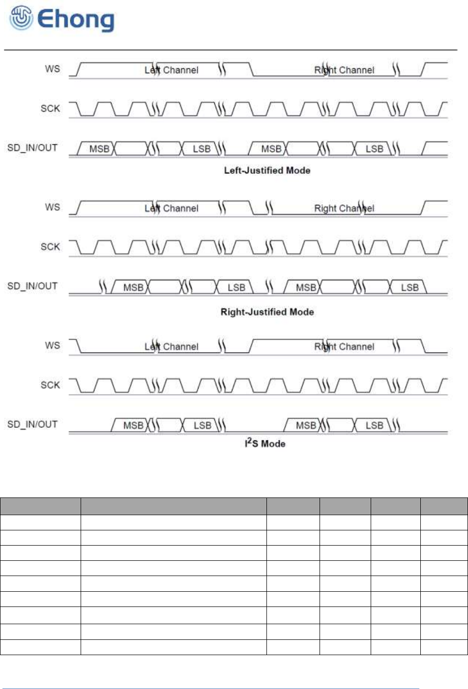
The digital audio interface supports the industry standard formats for I2S, left-justified or right-
justified. The interface shares the same pins of the PCM interface as Table 11.
Special firmware is needed if I2S is used. Contact EHong for the special firmware when use
I2S as the interface between the module and the host or the codec. The I2S support following
formats,
Bluetooth Audio Module
Ehong Technology Co., Ltd
Figure 8 : Digital Audio Interface Modes
Symbol
Parameter
Min
Typical
Max
Unit
-
SCK Frequency
-
-
6.2
MHz
-
WS Frequency
-
-
96
kHz
tch
SCK high time
80
-
-
ns
tcl
SCK low time
80
-
-
ns
topd
SCK to SD_OUT delay
-
-
20
ns
tssu
WS to SCK set up time
20
-
-
ns
tsh
WS to SCK hold time
20
-
-
ns
tisu
SD_IN to SCK set-up time
20
-
-
ns
tih
SD_IN to SCK hold time
20
-
-
ns
Bluetooth Audio Module
Ehong Technology Co., Ltd
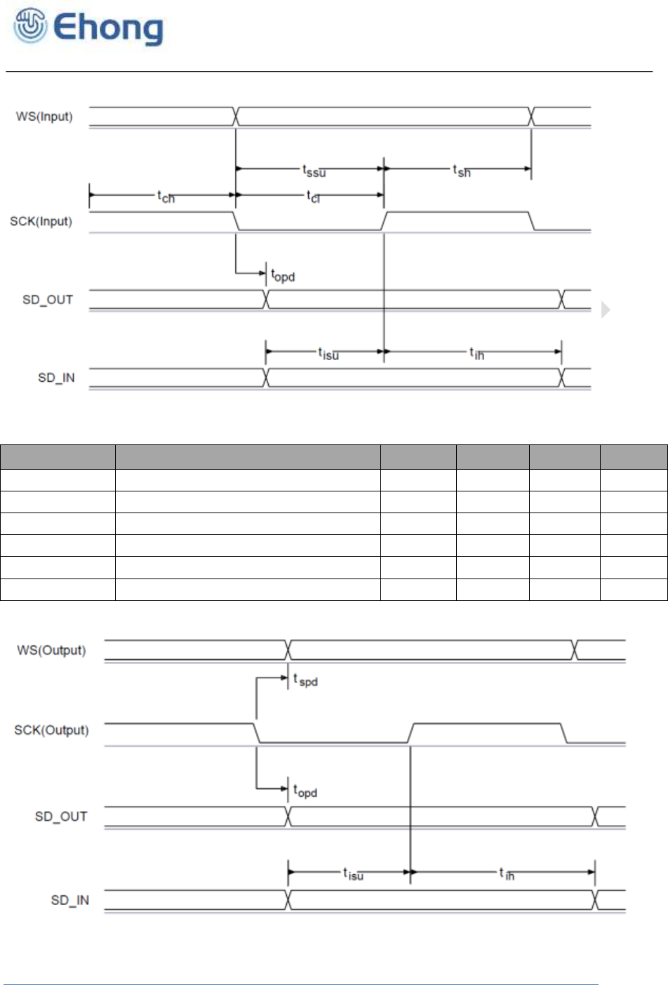
Table 12 : Digital Audio Interface Slave Timing
Figure 9 : Digital Audio Interface Slave Timing
Symbol
Parameter
Min
Typical
Max
Unit
-
SCK Frequency
-
-
6.2
MHz
-
WS Frequency
-
-
96
kHz
topd
SCK to SD_OUT delay
-
-
20
ns
tspd
SCK to WS delay
-
-
20
ns
tisu
SD_IN to SCK set-up time
20
-
-
ns
tih
SD_IN to SCK hold time
10
-
-
ns
Table 13 : Digital Audio Interface Master Timing
Figure 10 : Digital Audio Interface Master Timing
Bluetooth Audio Module
Ehong Technology Co., Ltd
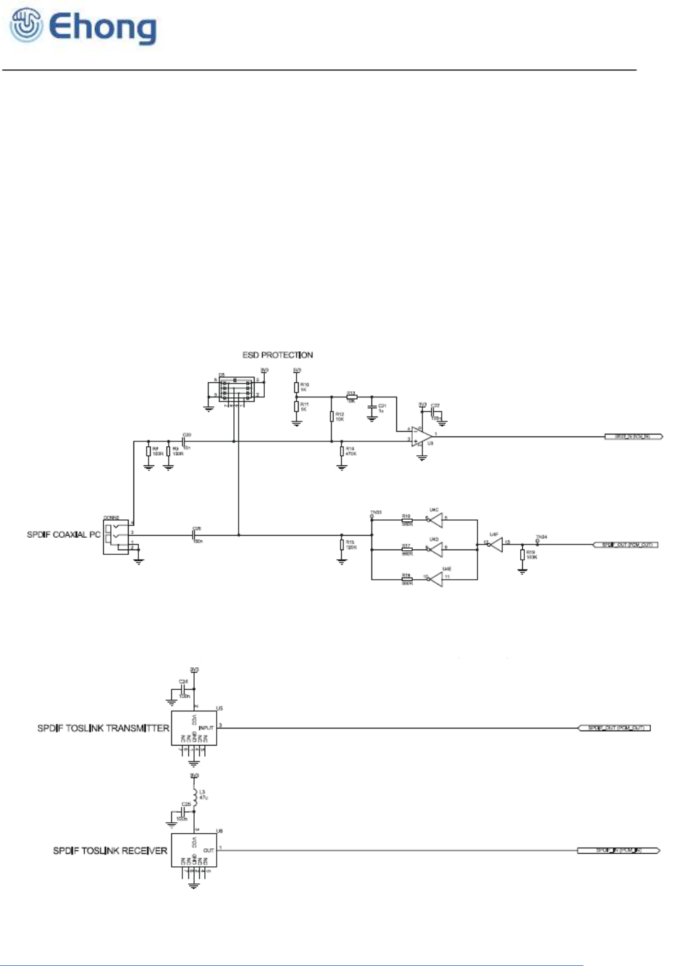
6.9.3. IEC 60958 Interface (SPDIF)
The IEC 60958 interface is a digital audio interface that uses bi-phase coding to minimise the
DC content of the
transmitted signal
and allows the
receiver
to
decode
the clock
information
from the
transmitted signal.
The IEC 60958 specification is based on the 2 industry standards:
■ AES/EBU
■ Sony and Philips interface specification SPDIF
The interface is compatible with IEC 60958-1, IEC 60958-3 and IEC 60958-4.
The SPDIF interface signals are SPDIF_IN and SPDIF_OUT and are shared on the PCM
interface pins. The input and output stages of the SPDIF pins can interface to:
■ A 75Ω coaxial cable with an RCA connector, see Figure 11.
■ An optical link that uses Toslink optical components, see Figure 12.
Figure 11: Example Circuit for SPDIF Interface (Co-Axial)
Figure 12: Example Circuit for SPDIF Interface (Optical)
Bluetooth Audio Module
Ehong Technology Co., Ltd
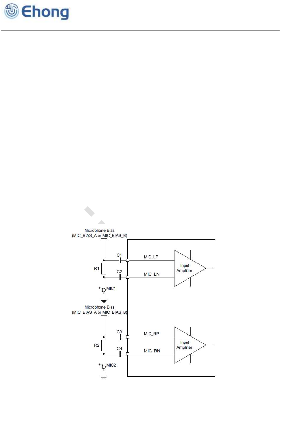
6.10. Microphone input
The module contains 2
independent
low-noise
microphone
bias
generators.
The
microphone
bias
generators
are recommended for biasing electret condensor
microphones. Figure 9.6 shows a biasing circuit for microphones with a sensitivity
between about ‑40 to ‑60dB (0dB = 1V/Pa):
Where:
■ The microphone bias generators derives their power from VBAT or VOUT_3V3 \
and requires no capacitor on its output.
■ The microphone bias generators maintains regulation within the limits 70μA to
2.8mA, supporting a 2mA source typically required by 2 electret condensor
microphones. If the microphone sits below these limits, then the microphone
output must be pre-loaded with a large value resistor to ground.
■ Biasing resistors R1 and R2 equal 2.2kΩ.
■ The input impedance at MIC_LN, MIC_LP, MIC_RN and MIC_RP is typically 6kΩ.
■ C1, C2, C3 and C4 are 100/150nF if bass roll-off is required to limit wind noise on the
microphone.
■ R1 and R2 set the microphone load impedance and are normally around 2.2kΩ.
Figure 13: Microphone Biasing (Single Channel
Shown)
Bluetooth Audio Module
Ehong Technology Co., Ltd
The microphone bias characteristics include:
■ Power supply:
■ CSR8670 BGA microphone supply is VBAT (via SMP_VBAT) or VOUT_3V3 (via SMPS_3V3)
■ Minimum input voltage = Output voltage + drop-out voltage
■ Maximum input voltage is 4.25V
■ Drop-out voltage:
■ 300mV maximum
■ Output voltage:
■ 1.8V or 2.6V
■ Tolerance 90% to 110%
■ Output current:
■ 70μA to 2.8mA
■ No load capacitor required
6.11. Analog Output stage
The output stage digital circuitry converts the signal from 16-bit per sample, linear PCM of
variable sampling frequency to a 2Mbits/s 5-bit multi-bit bit stream, which is fed into the analogue
output circuitry.
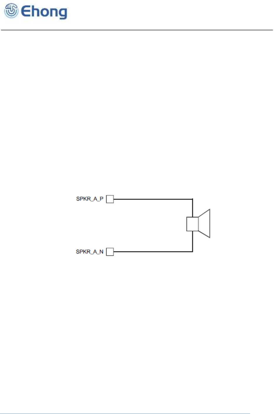
The output stage circuit is comprised a DAC with gain setting and class AB amplifier. The output
is available as a differential signal between SPKR_A_N and SPKR_L_P for the right channel, as
Figure 6 shows, and between SPKL_B_N and SPKL_B_P for the left channel.
Figure 14: Speaker output
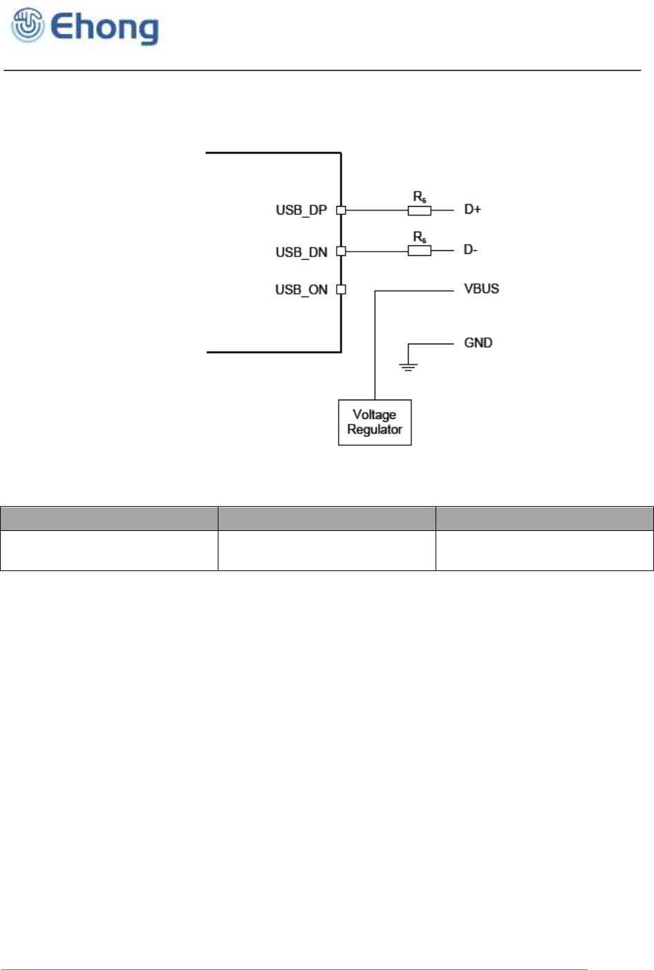
6.12. USB
This is a full speed (12M bits/s) USB interface for communicating with other compatible digital
devices. The module acts as a USB peripheral, responding to request from a master host
controller, such as a PC.
The USB interface is capable of driving a USB cable directly. No external USB transceiver is
required. The device operates as a USB peripheral, responding to requests from a master host
controller such as a PC. Both the OHCI and the UHCI standards are supported. The set of USB
endpoints implemented can behave as specified in the USB section of the Bluetooth
specification v2.1+EDR or alternatively can appear as a set of endpoints appropriate to USB
audio devices such as speakers.
Bluetooth Audio Module
Ehong Technology Co., Ltd
The module has an internal USB pull-up resistor. This pulls the USB_DP pin weakly high when
module is ready to enumerate. It signals to the USB master that it is a full speed (12Mbit/s) USB
device.
Figure 15: USB Connections
Identifier
Value
Function
Rs
27Ω Nominal
Impedance matching to USB
cable
Table 14: USB Interface Component Values
Note:
USB_ON is only used when the firmware need an input to detect if USB is connected and the USB
function shall be enabled. In such case it is shared with the module PIO terminals. If detection is not
needed (firmware already runs with USB, such as USB DFU or USB CDC), USB_ON is not needed.
Bluetooth Audio Module
Ehong Technology Co., Ltd
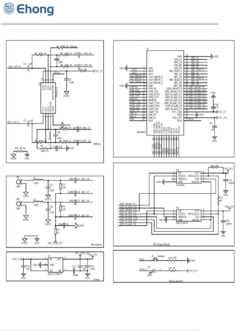
7. EH-MB18 Reference Design
Figure 16: Reference Design
Bluetooth Audio Module
Ehong Technology Co., Ltd
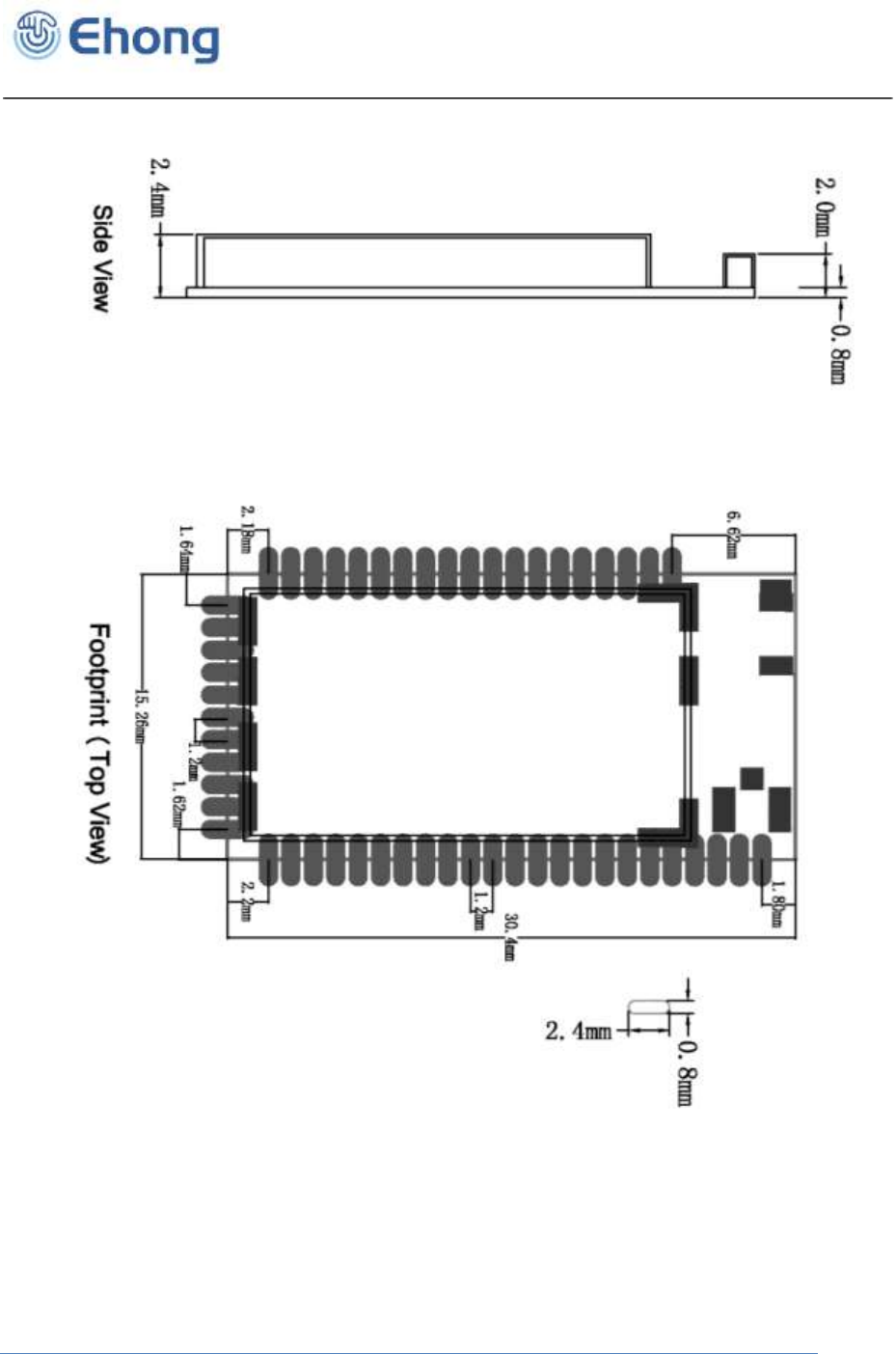
8. Mechanical and PCB Footprint Characteristics
Figure 17: Recommended PCB Mounting Pattern (Unit: mm, Deviation:0.02mm)TOP View
Bluetooth Audio Module
Ehong Technology Co., Ltd
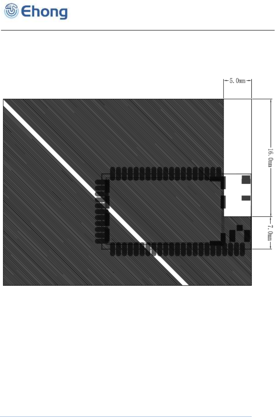
9. RF Layout Guidelines
EH-MB18 RF design to ensure enough clearance area of antenna, area length is 1.6 times of
antenna length, area width is 4 times of antenna width, the bigger the better if the space allows.
Module antenna clearance area size, as follows.
Figure 18: Clearance Area of Antenna
Bluetooth Audio Module
Ehong Technology Co., Ltd
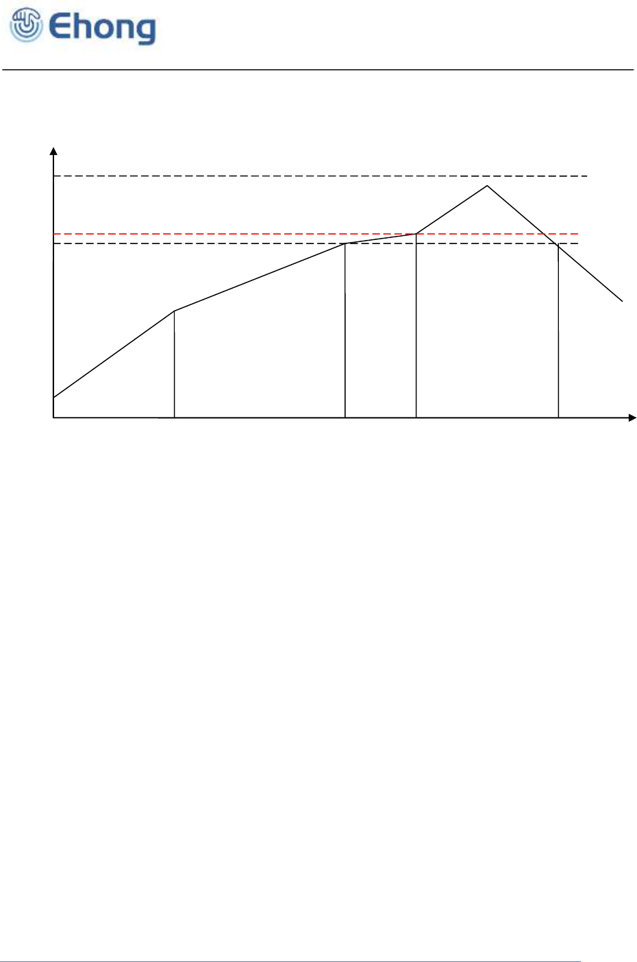
10. Reflow Profile
The soldering profile depends on various parameters necessitating a set up for each application.
The data here is given only for guidance on solder reflow.
210
217
℃
250
A B C D
1 2
0
25
3 4 5 6 min
E
Figure 19: Recommended Reflow Profile
Pre-heat zone (A) — This zone raises the temperature at a controlled rate, typically 0.5 – 2
C/s. The purpose of this zone is to preheat the PCB board and components to 120 ~ 150 C.
This stage is required to distribute the heat uniformly to the PCB board and completely remove
solvent to reduce the heat shock to components.
Equilibrium Zone 1 (B) — In this stage the flux becomes soft and uniformly encapsulates
solder particles and spread over PCB board, preventing them from being re-oxidized. Also with
elevation of temperature and liquefaction of flux, each activator and rosin get activated and start
eliminating oxide film formed on the surface of each solder particle and PCB board. The
temperature is recommended to be 150 to 210 for 60 to 120 second for this zone.
Equilibrium Zone 2 (c) (optional) — In order to resolve the upright component issue, it is
recommended to keep the temperature in 210 – 217 for about 20 to 30 second.
Reflow Zone (D) — The profile in the figure is designed for Sn/Ag3.0/Cu0.5. It can be a
reference for other lead-free solder. The peak temperature should be high enough to achieve
good wetting but not so high as to cause component discoloration or damage. Excessive
soldering time can lead to intermetallic growth which can result in a brittle joint. The
recommended peak temperature (Tp) is 230 ~ 250 C. The soldering time should be 30 to 90
second when the temperature is above 217 C.
Cooling Zone (E) — The cooling ate should be fast, to keep the solder grains small which will
give a longerlasting joint. Typical cooling rate should be 4 C.


NOTE: This equipment has been tested and found to comply with the limits for a Class B digital
device, pursuant to part 15 of the FCC Rules. These limits are designed to provide reasonable protection
against harmful interference in a residential installation. This equipment generates, uses and can radiate
radio frequency energy and, if not installed and used in accordance with the instructions, may cause
harmful interference to radio communications. However, there is no guarantee that interference will not
occur in a particular installation. If this equipment does cause harmful interference to radio or television
reception, which can be determined by turning the equipment off and on, the user is encouraged to try to
correct the interference by one or more of the following measures:
—Reorient or relocate the receiving antenna.
—Increase the separation between the equipment and receiver.
—Connect the equipment into an outlet on a circuit different from that to which the receiver is
connected.
—Consult the dealer or an experienced radio/TV technician for help.
Thisdevicecomplieswithpart15oftheFCCrules.Operationissubjecttothefollowingtwo
conditions:
(1)thisdevicemaynotcauseharmfulinterference,and
(2)thisdevicemustacceptanyinterferencereceived,includinginterferencethatmaycause
undesiredoperation.
Changesormodificationstothisunitnotexpresslyapprovedbythepartyresponsiblefor
compliancecouldvoidtheuser'sauthoritytooperatetheequipment.
Integrator is reminded to assure that these installation instructions
will not be made available to the end-user of the final host device.
the Integrator will be responsible to satisfy SAR/ RF Exposure requirements,
when the module integrated into any (portable, mobile, fixed) host device.
The final host device, into which this RF Module is integrated" has to be labelled
with an auxilliary lable stating the FCC ID of the RF Module, such as
"Contains FCC ID: 2ACCRMB18".