ShenZhen Doctors of Intelligence and Technology ESP-F ESP-F WiFi Module User Manual UserManualForESP F doit V1 1
ShenZhen Doctors of Intelligence & Technology Ltd. ESP-F WiFi Module UserManualForESP F doit V1 1
User Manual

D
F
e
ES
P
Ma
n
D
OIT.
e
atures
SOC cha
r
Built
-
cons
u
can
b
RTO
S
Built
-
Built
-
The
I2C,
I
The
d
cut-o
f
Can
b
trans
m
the c
(DTI
M
Wi-Fi ch
a
Supp
o
Supp
o
Soft
A
Supp
o
Supp
o
(CB
C
RC4)
P2P
f
powe
WP
A
Supp
o
and
T
Supp
o
802.1
Supp
o
Supp
o
upda
t
Supp
o
and i
O
P
-F
n
ual
AM
®
Doctors of
I
r
acteristics
-
in Tensilic
a
u
mption 32-
b
b
e 80MHz
a
S
;
-
in TCP/IP p
r
-
in 1 channel
outside inte
r
I
2S, IR Rem
o
d
eep-sleep c
u
f
f current is
s
b
e wake-up
w
m
it data pac
k
onsume po
w
M
3) when at
a
racteristics
o
rt 802.11 b/
g
o
rt three m
o
A
P+STA;
o
rt Wi-Fi Di
r
o
rt hardwar
e
C
-MAC, com
p
)
, WAPI(SM
S
f
ind, P2P G
O
e
r manageme
n
A
/PA2 PSK a
n
o
rt 802.11 i
T
SN;
o
rt 802.11n (
1
h/RFC1042
f
o
rt seamless
r
o
rt AT remo
t
t
ion;
o
rt SmartC
o
O
S device S
m
Ver V1
I
ntelligence
&
a
L106 ul
t
b
it cpu, the
m
a
nd 160MH
z
r
otocol stack
;
10-
b
it high
p
r
faces have
o
te Control,
P
u
rrent is abou
t
s
maller than
5
w
ithin 2 ms,
k
age;
w
er is small
e
standby stat
u
g
/n/e/i
o
des: Statio
n
r
ect(P2P);
e
accelerati
o
p
utation mo
d
S
4), WEP(R
C
O
mode/GC
n
t;
n
d WPS;
security:
p
2.4 GHz);
f
rame encap
s
r
oam;
t
e updation
a
o
nfig functio
n
m
artConfig.
Do
c
ESP
-
.1
&
Technolog
y
t
ra-low po
w
m
ain freque
n
z
, also supp
o
;
p
recision AD
HSPI, UA
R
P
WM, GPIO;
t
10uA, and
t
5
uA;
and connect
e
r than 1.0
m
u
s;
n
, SoftAP,
a
o
n for CC
M
d
e), TKIP (M
C
4), CRC;
mode and P
2
p
re-certificati
s
ulation;
a
nd cloud O
T
n
for Andr
o
c
tors of In
t
-
F Wi
F
Mar.
,
y
Co., LTD (
w
er
n
cy
o
rt
C;
R
T,
;
t
he
to
m
W
a
nd
M
P
M
IC,
2P
i
on
T
A
o
id
P
A
●
●
●
●
●
●
●
●
●
●
M
M
t
elligence
F
i Modul
e
,
18, 2017
w
ww.doit.a
m
P
eripher
a
2*U
A
1*E
n
1*A
D
1*w
a
1*H
1*I
2
1*I
2
4M
b
MA
X
Workin
g
Module
s
A
pplicati
o
Serial Trans
p
WiFi probe
r
Smart powe
r
Mesh netwo
Sensor netw
Wearable el
e
Securit ID l
a
Wireless lo
c
Wireless lo
c
Industrial w
i
M
odule T
y
Name
ESP-F
M
odule S
t
& Techn
o
e
Nu
m
m
) Copyright
@
a
l for Mo
d
A
RT;
n
;
D
C
a
keup pin
S
PI
C
S
b
yte Flash
X
11* GPIO
s
g
temperatu
r
s
ize: 16mm*
2
o
ns
p
arent trans
m
;
r
plug/Smart
r
ks;
o
rks;
e
ctronics;
a
bel;
ation recogn
i
ation system
i
reless contr
o
y
pe
Anten
n
PCB o
n
t
ructure
o
logy Co.
m
.: DM001
2
@
2014-2017
d
ule
s
;
r
e: -40℃-85
℃
2
4mm;
m
ission;
LED light;
i
tion;
beacon;
o
l.
n
a Type
n board ant
e
, LTD
2
CN
℃
nna
HuDun Demo
DOIT.AM® Datasheet Page 2
ESP-F
ESP8266EX
802.11 b/g/n/e/i
MAC
Interface
SRAM
Power
Mangement
RF Transceiver
Digital base
Crystal oscillator
Bias Circuit
PCB Ant.
4M bytes
SPI FLASH
SDIO
3.3V
GPIO
UART
I2C
SPI
ADC
I2S
Achieve Update
Date Version Update
Mar, 21, 2017 V1.0 Ver 1.0
HuDun Demo

DOIT.AM®
Doctors of Intelligence & Technology Co. Ltd (www.doit.am) Copyright@2014-2017
Context
Figures ................................................................................................................................... 4
Table ...................................................................................................................................... 4
1. Introduction ....................................................................................................................... 1
2. Interface Definition ........................................................................................................... 3
3. Shape and Size ................................................................................................................... 5
4. Electronical Characteristics ............................................................................................... 6
5. Power Consumption ......................................................................................................... 6
6. Wi-Fi RF Characteristics ................................................................................................... 7
7. The Recommended Sold Temperature Curve .................................................................. 8
8. Schematics for ESP-F ........................................................................................................ 8
9. Minimum System .............................................................................................................. 9
10. The Recommended PCB Design ................................................................................... 11
11. Peripheral Line Suggestion ........................................................................................... 12
Appendix. ............................................................................................................................ 13
HuDun Demo

DOIT.AM®
Doctors of Intelligence & Technology Co. Ltd (www.doit.am) Copyright@2014-2017
Figures
Fig. 1.1 Module Structure ..................................................................................................................................................... 1
Fig. 2.1 ESP-F Definition for Pins ........................................................................................................................................ 3
Fig. 3.1 Shape for ESP-F ....................................................................................................................................................... 5
Fig. 3.2 Size for ESP-F ......................................................................................................................................................... 5
Fig. 7.1 Temperature Curve when Sold ................................................................................................................................ 8
Fig. 9. 1 Minimum System .................................................................................................................................................... 9
Fig. 10.1 scheme1: Antenna is at the outside of the board .................................................................................................. 11
Fig. 10.2 Scheme 2: Antenna is placed along with side of the board, and it is blank at the bottom of the board. ............. 11
Fig. 10.3 Scheme 3: Antenna is placed along with the side of the board, and don’t cover copper under the module........ 12
Table
Table 1.1 Parameters for ESP-F ............................................................................................................................................ 2
Table 2.1 Pin Modes ............................................................................................................................................................. 3
Table 2.2 Function Definition of Module Pins ...................................................................................................................... 4
Table 3.1 Size for ESP-F ....................................................................................................................................................... 5
Table 4.1 Electronics ............................................................................................................................................................. 6
Table 5.1 Power Consumption ............................................................................................................................................. 6
Table 6.1 Wi-Fi RF Characteristics ....................................................................................................................................... 7
HuDun Demo

DOIT.AM®
ESP-F User Manual
Doctors of Intelligence & Technology (DOIT)(www.doit.am) Copyright@2014-2017 Page 1
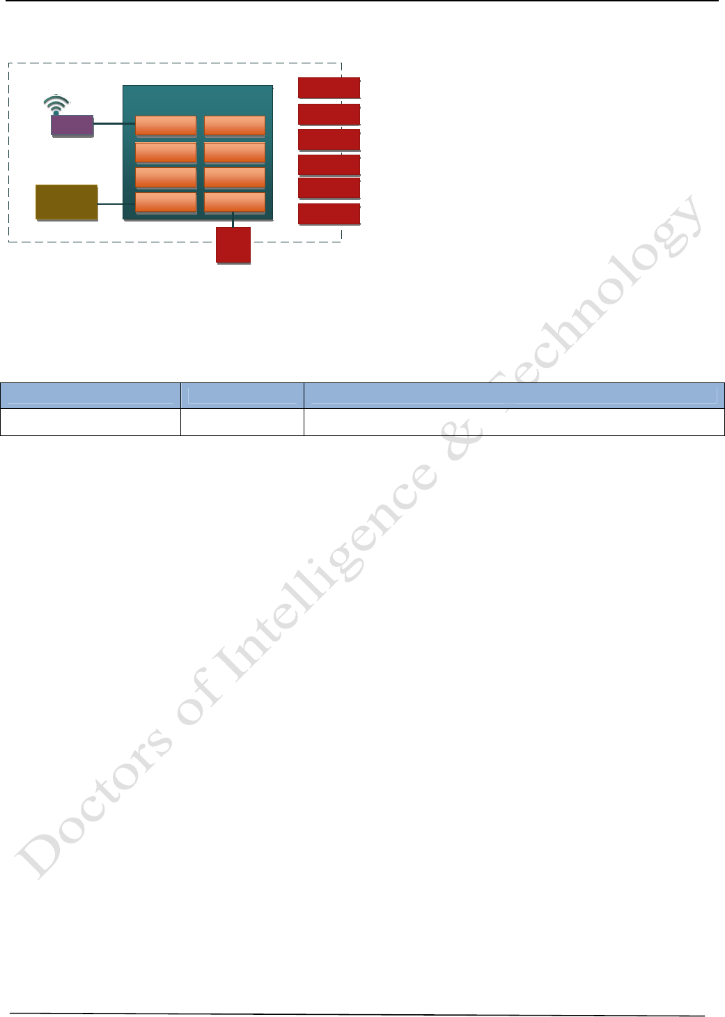
1. Introduction
The WiFi module ESP-F is manufactured by using a high-performance chip ESP8266EX. This small
chip is encapsulated an enhanced Tensilica’s L106 diamond series 32-bit kennel CPU with a SRAM.
Thus, ESP8285 has the complete function Wi-Fi function; it not only can be applied independently, but
can be used as a slaver working with other host CPU. When ESP8285 is applied as a slaver, it can start
from the onboard Flash. The built-in high-speed buffer is not only benefit to improve the system
performance, but optimize the store system. In addition, ESP8285 can be used as Wi-Fi adapter by
SPI/SDIO or I2C/UART interface, when it is applied to other MCU design.
The ESP-F module supports the standard IEEE802.11 b/g/n/e/i protocol and the complete TCP/IP
protocol stack. User can use it to add the WiFi function for the installed devices, and also can be viewed
as a independent network controller. Anyway, ESP-F module provides many probabilities with the best
price.
ESP8266EX
802.11 b/g/n/e/i
MAC
Interface
SRAM
Power
Mangement
RF Transceiver
Digital base Crystal oscillator
Bias Circuit
PCB Ant.
4M bytes
SPI FLASH
SDIO
3.3V
GPIO
UART
I2C
SPI
ADC
I2S
Fig. 1.1 Module Structure
HuDun Demo

DOIT.AM®
ESP-F User Manual
Doctors of Intelligence & Technology (DOIT)(www.doit.am) Copyright@2014-2017 Page 2
Parameters for ESP-F are listed as follows.
Table 1.1 Parameters for ESP-F
Types Items Parameters
Wi-Fi
Frequency scope 2.4G~2.5G(2400M~2483.5M)
Transmit power
802.11b: +20 dBm
802.11g: +17 dBm
802.11n: +14 dBm
Receiving sensitivity
802.11b: -91 dbm (11Mbps)
802.11g: -75 dbm(54Mbps)
802.11n: -72 dbm(MCS7)
Antenna PCB onboard antenna
Hardware
CPU Tensilica L106 32 bit MCU
Perpherl
UART/SDIO/SPI/I2C/I2S/IR control
GPIO/ADC/PWM/SPI/I2C/I2S
Working voltage 2.5V ~ 3.6V
Working current Average current: 80 mA
Working temperature -40°C ~85°C
Environment
temperature
-40°C ~ 85°C
Size 16mm x 24mm x 3mm
Software
Wi-Fi mode Station/SoftAP/SoftAP+Station
Security mode WPA/WPA2
Encryption type WEP/TKIP/AES
Update firmware UART Download/OTA (by internet)
Software develop Non-RTOS/RTOS/Arduino IDE etc.
Network protocol IPv4, TCP/UDP/HTTP/FTP/MQTT
User configuration AT+ command/cloud sever/ Android/iOS APP
HuDun Demo

DOIT.AM®
ESP-F User Manual
Doctors of Intelligence & Technology (DOIT)(www.doit.am) Copyright@2014-2017 Page 3
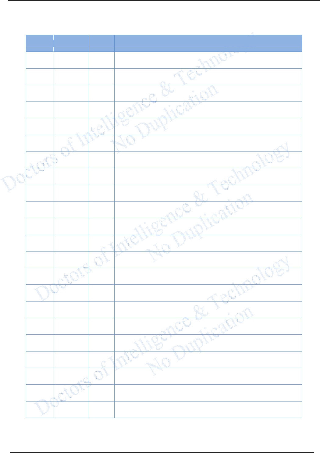
2. Interface Definition
Interface definition of ESP-F can be shown in the following.
1 2 43 5 6 7 8
15 16 1817 19 20 21 22
910 12
11 13 14
ESP-F
RST
ADC
EN
IO14
IO12
IO13
VCC
IO16
TXD0
RXD0
IO5
IO0
IO2
IO15
GND
IO4
GPIO1
GPIO3
FLASH
TXD1
U0RTS
HSCK
HMISO
HMOSI
3.3V
U0CTS
SLEEP
CS0
MISO
IO9
IO10
MOSI
SCK
Fig. 2.1 ESP-F Definition for Pins
Working mode and definition of pins:
Table 2.1 Pin Modes
Mode GPIO15 GPIO0 GPIO2
UART download
low
low high
Flash
Boot
mode
low
high high
HuDun Demo
DOIT.AM®
ESP-F User Manual
Doctors of Intelligence & Technology (DOIT)(www.doit.am) Copyright@2014-2017 Page 4
Table 2.2 Function Definition of Module Pins
Num Pin Type Function
1
RST
I Reset the signal outside (enable with low), Reset module
2
ADC I A/D pin. Input voltage
0
~1V, value:
0
~1024
3
EN
I Enable, high level: chip work normally; low level: chip closes with
small current.
4
IO16
I/O deep sleep/wakeup
5
IO14
I/O
GPIO14; HS
PI_CLK
6
IO12
I/O
GPIO12;HS
P
I_MISO
7
IO13
I/O
GPIO13;
HSPI_MOSI; U
A
R
T0
_C
TS
8
VCC P Module working voltage:
3.3V
9
CS0
I/O GPIO11; SD_CMD; SPI_CS0
10 MISO
I/O GPIO7; SD_D0, SPI_MSIO
11 IO9
I/O
GPIO9; SD_D2 PIHD; HSPIHD
12 IO10
I/O
GPIO10; SD_D3;
SPIWP; HSPIWP1
13 MOSI
I/O
GPIO8; SD_D1;
SPI_MOSI1
14 SCLK
I/O GPIO6; SD_CLK; SPI_CLK
15 GND
P GND
16 IO15
I/O
GPIO15;
MTDO;HSPICS;
U
AR
T0_RT
S
17 IO2
I/O
GPIO2;
U
AR
T1
_T
XD
18 IO0
I/O
GPIO0;
SPI_CS2
19 IO4
I/O
GPIO4
20 IO5
I/O
GPIO5
21 RXD
I/O
GPIO3; used to build in Flash as UART Rx
22 TXD
I/O
GPIO1;
used to build in Flash as UART Tx
HuDun Demo
D
3
.
Fl
a
L
2
D
OIT.
Doc
t
.
Shape
a
Shape a
n
a
sh is 4M
b
L
ength
4.5mm
AM
®
t
ors of Intell
i
a
nd Siz
e
n
d size for
b
ytes (32M
b
Wi
d
14
m
i
gence & Te
c
e
this modu
l
b
its).
d
th
m
m
c
hnology (D
O
l
e can be s
h
Fig. 3.
(a)
(
b
Fig. 3
Table
3
Heigh
t
3
mm
ESP-F Us
e
O
IT)(www.d
o
hown as f
o
1 Shape fo
r
Vertical V
b
) Side Vi
e
3
.2 Size for
3
.1 Size fo
r
t
e
r Manual
o
it.am) Copy
r
o
llows. Its
s
r
ESP-F
iew
w
ESP-F
r
ESP-F
Pin
4 x
2
r
ight@2014-
2
s
ize is 16
m
2
017
m
m*24mm*
Distance b
e
2.54
Pa
g
3mm, and
e
tween Pins
g
e 5
the
HuDun Demo

DOIT.AM®
ESP-F User Manual
Doctors of Intelligence & Technology (DOIT)(www.doit.am) Copyright@2014-2017 Page 6
4. Electronical Characteristics
Table 4.1 Electronics
Parameters Condition Min Classical Max Unite
Store Temperature - -40 Normal 125 ℃
Sold Temperature IPC/JEDEC
J-STD-020 - - 260 ℃
Working Voltage - 2.5 3.3 3.6 V
I/O
VIL/VIH - -0.3/0.75VIO - 0.25VIO/3.6 V
VOL/VOH - N/0.8VIO - 0.1VIO/N
IMAX - - - 12 mA
Electrostatic release
quantity (Human model) TAMB=25℃ - - 2 KV
Electrostatic release
quantity (Human model) TAMB=25℃ - - 0.5 KV
5. Power Consumption
Table 5.1 Power Consumption
Parameters Min Classical Max Unite
Tx802.11b, CCK 11Mbps, POUT=+17dBm - 170 - mA
Tx802.11g, OFDM 54 Mbps, POUT =+15dBm - 140 - mA
Tx802.11n,MCS7,POUT =+13dBm - 120 - mA
Rx 802.11b,1024 Bytes, -80dBm - 50 - mA
Rx 802.11g,1024 Bytes, -70dBm - 56 - mA
Rx 802.11n,1024 Bytes, -65dBm - 56 - mA
Modem-sleep① - 15 - mA
Light-sleep② - 0.9 - mA
Deep-sleep③ - 20 - μA
close - 0.5 - μA
Note
①: Modem-Sleep mode can be used for the case that CPU is always working, e.g., PWM or I2S etc. If
WiFi is connected and no data is to transmitted, in this case, WiFi modem can be closed to save power
energy. For example, if at DTIM3 status, keep asleep at 300ms, Then, the module can wake up to receive
the Beacon package within 3ms and the current being 15mA.
②: Light-Sleep mode can used for the case that CUP can stop the application temporally, e.g., Wi-Fi
Switch . If Wi-Fi is connected and there is no data packet to transmitted, by the 802.11 standard (e.g., U-
HuDun Demo
DOIT.AM®
ESP-F User Manual
Doctors of Intelligence & Technology (DOIT)(www.doit.am) Copyright@2014-2017 Page 7
APSD), module can close Wi-Fi Modem and stop CPU to save power. For example, at DTIM3, keep up
sleeping at 300ms, it would receive the Beacon package from AP after each 3ms, then the whole average
current is about 0.9mA.
③ Deep-Sleep mode is applied to the case that Wi-Fi is not necessary to connect all the time, just send
a data packet after a long time (e.g., transmit one temperate data each 100s) . it just need 0.3s-1s to
connect AP after each 300s, and the whole average current is much smaller 1mA.
6. Wi-Fi RF Characteristics
The data in the following Table is gotten when voltage is 3.3V and1.1V in the indoor temperature
environment.
Table 6.1 Wi-Fi RF Characteristics
Parameters Min Classical Max Unite
Input frequencey 2412 - 2484 MHz
Input impedance - 50 - Ω
Input reflection - - -10 dB
At 72.2Mbps, output power consumption for PA 15.5 16.5 17.5 dBm
At 11b mode, output power consumption for PA 19.5 20.5 21.5 dBm
Sensibility - - - -
DSSS, 1Mbps - -98 - dBm
CCK11, Mbps - -91 - dBm
6Mbps(1/2 BPSK) - -93 - dBm
54Mbps(3/4 64-QAM) - -75 - dBm
HT20, MCS7(65 Mbps, 72.2 Mbps) - -72 - dBm
Adjacent Inhibition
OFDM, 6Mbps - 37 - dB
OFDM, 54Mbps - 21 - dB
HT20, MCS0 - 37 - dB
HT20, MCS7 - 20 - dB
HuDun Demo
D
7
.
8
.
D
OIT.
Doc
t
.
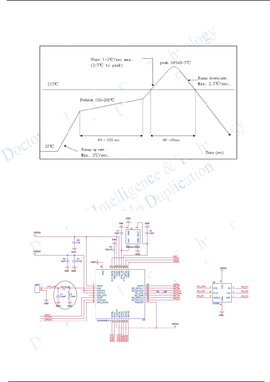
The R
e
.
Schem
a
AM
®
t
ors of Intell
i
e
comme
a
tics for
i
gence & Te
c
nded S
o
Fi
g
ESP-F
c
hnology (D
O
ld Tem
p
g
. 7.1 Tem
p
ESP-F Us
e
O
IT)(www.d
o
p
erature
p
erature Cu
r
e
r Manual
o
it.am) Copy
r
Curve
r
ve when S
r
ight@2014-
2
o
l
d
2
017 Pa
g
g
e 8
HuDun Demo

D
9
.
i
s
D
OIT.
Doc
t
.
Minim
u
This mod
u
Note
(1) the
w
(2) the
m
(3) RST
(4) WiF
i
s
at workin
g
AM
®
t
ors of Intell
i
u
m Syst
e
u
le can work
j
w
orking vol
t
m
ax current
Pin is ena
b
i
module is
g
mode: G
P
i
gence & Te
c
e
m
j
ust at 3.3V
w
t
age for mo
from IO o
f
b
led when i
t
at update
m
P
IO0 is at h
i
c
hnology (D
O
Fig. 8.1 S
w
orking volt
a
Fig. 9.
1
dule is DC
f
this modul
e
is low lev
e
m
ode: GPI
O
i
gh level, a
n
ESP-F Us
e
O
IT)(www.d
o
chematics
a
ge.
1
Minimu
m
3.3V;
e is 12mA;
e
l; and EN
p
O
0 is low le
v
n
d then res
e
e
r Manual
o
it.am) Copy
r
for ESP-
F
m
System
p
in is enabl
e
v
el, then m
e
t to power;
r
ight@2014-
2
e
d when it i
o
dule reset
2
017
i
s high leve
l
to power;
Pa
g
l
;
Wi-Fi mo
d
g
e 9
d
ule
HuDun Demo

DOIT.AM®
ESP-F User Manual
Doctors of Intelligence & Technology (DOIT)(www.doit.am) Copyright@2014-2017 Page 10
(5) Wi-Fi module is connected to RXD of the other MCU, and TXD is connected to RXD of the
other MCU.
HuDun Demo

DOIT.AM®
ESP-F User Manual
Doctors of Intelligence & Technology (DOIT)(www.doit.am) Copyright@2014-2017 Page 11
10. The Recommended PCB Design
Wi-Fi module can be inserted into the PCB board directly. For the high RF performance for the end
device, please note the placement for the antenna and the module.
It is suggested that the module is placed along with PCB side, the antenna is placed outside the board,
or along with the PCB side, and the below board is blank, please refer to the scheme 1 and scheme 2; if
the PCB antenna must placed on the board, please do not cover the copper at the bottom of PCB antenna,
as can be shown at scheme 3.
Mainboard
6.6mm
810911 12 13 14
ESP-F
15
16
1 2 43 5 6 7
Fig. 10.1 scheme1: Antenna is at the outside of the board
Main
Board
5mm
6.6mm
5mm
810911 12 13 14
ESP-F
15
16
1 2 43 5 6 7
Fig. 10.2 Scheme 2: Antenna is placed along with side of the board, and it is blank at the bottom of the
board.
HuDun Demo

DOIT.AM®
ESP-F User Manual
Doctors of Intelligence & Technology (DOIT)(www.doit.am) Copyright@2014-2017 Page 12
MainBoard
5mm
6.6mm
5mm
810911 12 13 14
ESP-F
15
16
1 2 43 5 6 7
Fig. 10.3 Scheme 3: Antenna is placed along with the side of the board, and don’t cover copper under the
module
11. Peripheral Line Suggestion
Wi-Fi module is already integrated into high-speed GPIO and Peripheral interface, which may be
generated the switch noise. If there is a high request for the power consumption and EMI characteristics,
it is suggested to connect a serial 10~100 ohm resistance, which can suppress overshoot when switching
power supply, and can smooth signal. At the same time, it also can, to a certain extent, prevent
electrostatic discharge (ESD).
HuDun Demo

D
D
n
o
m
e
pr
e
re
s
a
n
li
c
T
A
th
e
D
OIT.
Doct
o
D
isclai
m
The infor
m
o
tice.
Document
s
e
rchantabil
i
e
sented by
s
ponsibilit
y
n
y patent r
i
c
ensing, wh
e
T
he Wi-Fi a
A
ll the me
n
e
property
o
AM
®
o
rs of Intelli
g
m
er a
n
m
ation in th
i
s
are prov
i
i
ty, suitabl
e
any propo
y
, including
i
ghts. This
e
ther expre
s
lliance mar
k
n
tioned bra
n
o
f their res
p
g
ence & Tec
h
n
d C
o
i
s article, i
n
i
ded by t
h
e
for any p
a
sal, specifi
the use of
t
document
s
s or impli
e
k
s shall be
n
d names,
t
p
ective own
e
h
nology (DO
I
o
p
y
ri
gh
n
cluding th
e
h
e current
v
a
rticular pu
r
c
ation, or
s
t
he inform
a
in this, b
y
e
d license.
o
wned by t
h
t
rademarks
e
rs, and he
r
Noti
c
B
e
man
u
Tech
n
cont
e
remi
n
Doct
o
try t
h
man
u
is co
m
this
m
to pr
o
ESP-F Us
e
I
T)(www.doi
t
h
t No
t
e URL for
v
ersion wi
r
pose or n
o
s
ample me
n
a
tion within
y
estoppel
h
e Wi-Fi a
l
and regist
e
r
eby decl
a
r
e
c
e
e
cause of
t
u
al may
h
nology
C
e
nts of thi
n
ders. T
h
o
rs of Int
e
h
eir best t
o
u
al, but it
mpletely
m
anual, a
n
o
vide any
e
r Manual
t
.am) Copyri
g
t
ice
reference,
i
thout any
o
n-infringe
m
n
tioned els
e
this docu
m
or otherw
i
l
liance.
e
red tradem
e
.
t
he prod
u
change.
C
o., LTD
s manual
h
is manu
a
e
lligence
&
o
provide
does not
right and
n
d infor
m
express
o
g
ht@2014-2
0
i
f there is
a
guarantee
m
ent guara
n
e
where. T
h
m
ent produc
e
i
se, grant
a
a
rks prese
n
ct update
Doctors
K
eeps th
e
in the ab
s
a
l is us
e
&
Techno
the accur
a
ensure th
a
national,
m
ation an
d
o
r implied
0
17
a
ny change
,
responsibi
l
n
tees, and
a
h
is docume
n
ed by the i
n
a
ny intelle
c
n
ted in this
or other
r
of Int
e
e
right to
s
ence of
a
e
d only
a
o
logy Co.,
a
te infor
m
a
t the ma
n
all the s
t
d
advice
d
guarante
e
Pag
e
without p
r
l
ity, includ
i
a
ny guarant
e
n
t has no
a
n
fringemen
t
c
tual prop
e
document
r
easons, t
h
e
lligence
change
t
a
ny notice
a
s a gui
d
LTD wo
u
m
ation in t
h
n
ual cont
e
t
atements
d
o not m
e
e
s.
e
14
r
ior
i
ng
e
es
a
ny
t
of
e
rty
are
h
is
&
t
he
or
d
e,
u
ld
h
is
e
nt
in
e
an
HuDun Demo
This device complies with part 15 of the FCC Rules. Operation is subject to the following two conditions:
(1) this device may not cause harmful interference, and (2) this device must accept any interference received,
including interference that may cause undesired operation.
Any changes or modifications not expressly approved by the party responsible for compliance
could void the user's authority to operate the equipment.
NOTE: This equipment has been tested and found to comply with the limits for a Class B digital device,
pursuant to Part 15 of the FCC Rules. These limits are designed to provide reasonable protection against
harmful interference in a residential installation. This equipment generates, uses and can radiate radio frequency
energy and, if not installed and used in accordance with the instructions, may cause harmful interference to
radio communications. However, there is no guarantee that interference will not occur in a particular
installation.
If this equipment does cause harmful interference to radio or television reception,
which can be determined by turning the equipment off and on, the user is encouraged to try to correct the
interference by one or more of the following measures:
-- Reorient or relocate the receiving antenna.
-- Increase the separation between the equipment and receiver.
-- Connect the equipment into an outlet on a circuit different
from that to which the receiver is connected.
-- Consult the dealer or an experienced radio/TV technician for help.
The device has been evaluated to meet general RF exposure requirement. The device can be used in portable
exposure condition without restriction.
FCC ID: 2AL3B-ESP-F