Shi Xinzhongxin Technology F-6688 Bluetooth Module User Manual www i enet com
Shenzhenshi Xinzhongxin Technology Co., Ltd. Bluetooth Module www i enet com
15_F-6688 UserMan, r1.pdf

Page 1 of 14
BK8000LBluetooth Audio SoC UserGuide
F-6688
Brand:XINZHONGXIN
FCC ID:2AG94F-6688
Shenzhenshi Xinzhongxin Technology Co., Ltd.

BK8000L Datasheet
Page 2 of 14
Contents
1. General Description......................................................................................................................4
1.1. Features................................................................................................................................4 1.2. Applications.........................................................................................................................4
2. Pin Definition................................................................................................................................5
3. Functional Description.................................................................................................................7
3.1. GPIO.....................................................................................................................................7 3.2. PWM Timer and Watch Dog Timer...................................................................................8 3.3. Power Management.............................................................................................................8 3.4. MCU.....................................................................................................................................8 3.5. I2C and UART Interface.....................................................................................................8 3.6. FM Receiver Control Interface...........................................................................................8 3.7. FLASH Access Interface....................................................................................................9 3.8. SPI........................................................................................................................................9 3.9. SAR ADC and LED............................................................................................................9 3.10. Audio Peripheral..................................................................................................................9
4. Electrical Characteristics............................................................................................................10
4.1. Absolute Maximum Ratings.............................................................................................10 4.2. Recommended Operating Conditions..............................................................................10 4.3. System LDO......................................................................................................................10 4.4. Analog LDO/BUCK..........................................................................................................10 4.5. Digital LDO/BUCK..........................................................................................................11 4.6. USB LDO...........................................................................................................................11 4.7. Typical Power Consumption............................................................................................11 4.8. RF Characteristics.............................................................................................................11 4.9. Audio Characteristics........................................................................................................12
5. Application Schematic...............................................................................................................12
6. About the Qualification..............................................................................................................12
7. Package Information...................................................................................................................13
8. Ordering Information.................................................................................................................14
Low Power Bluetooth Audio SoC
Page 3 of 14
1.General Description
The BK8000L chip is a highly integrated single-chip Bluetooth audio device. It integrates the high-performance transceiver, rich features baseband processor, and Bluetooth audio profile. The BK8000L cache based architecture enables it is fully programmable with any application, that it may be used for control and multimedia hybrid application. The internal dual stereo ADC converts the stereo line in input to digital audio that enables the line in use the digital equalizer. Hardware equalizer and accelerator offload the MCU, and make it suitable for low power headset application.
1.1.Features
lOperation voltage from 2.8 V to 4.2 V
lBluetooth 2.1+EDR compliant
l-92 dBm sensitivity for 2 Mbps mode and 5 dBm transmit power
lA2DP v1.2, AVRCP v1.0 and HFP v1.5 profile
lIntegrated 96 dB SNR stereo ADC and stereo DAC
lFive bands hardware equalizer
lDigital equalizer for stereo line in
lHardware accelerator for low power
lFull duplex hands-free speakerphone
lUp to 250 mA charge controller
1.2.Applications
lBluetooth stereo speaker lBluetooth stereo headset lBluetooth control and multimedia hybrid
ROSC
XTAL
DPLL Power
Manage
ment
Switch
Regulator
Audio
DAC
Audio
ADC
LED
POR
MCU
with
JTAG
Reset
DMA
Watch
Dog
I2C
FLASH
Controller
I2C/
UART
ADC
80KB
Data
RAM
16KB
I-Cache
SPI
PMU
BIST
Bluetooth
Transceiver
PWM
Audio(inc.DTMF)
HWA
BK8000L Datasheet
Page 4 of 14
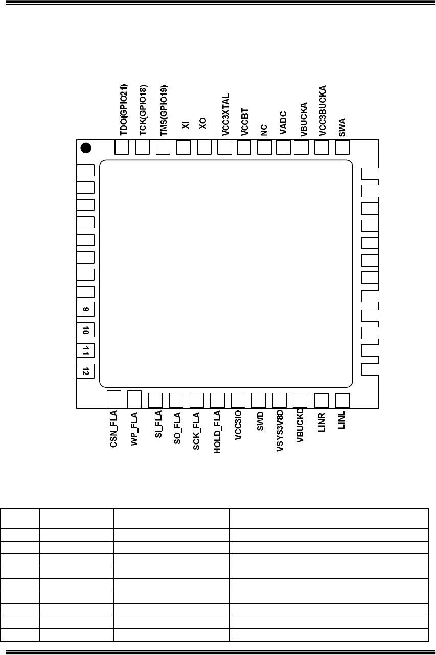
2.Pin Definition
It provides maximum QFN6x648-pins package for wireless audio application.
MICINN
TSTEN
1
2
3
4
5
6
1516171819
34
33
32
31
30
GNDPAD
BK8006
QFN6*648-Pin
29
AUDIORP
AUDIOLP
7
20
8
2122
35
36
RFP_BT
AUDIOLN
AUDIORN
GPIO0
GPIO1
2324
MICINP
1314
44 45 46 47 4843
RSTN
GPIO4
GPIO3
GPIO2
VDD12
GPIO11
V2MICBIAS
VREF1AUD
VCC3SYS
VCC5USB
VCC4BAT
GPIO5
VCCAUD
TDI(GPIO20)
28
27
26
25
41 424038 3937
Table 1 Pin Description of 48Pin Package
PINNamePin FunctionDescription
1
RSTNDigital I/OActive low reset 2
TSTENDigital I/OTest enable, high enable chip in test mode 3
RFP_BTRF port2.4 GHz antenna port 4
TDIDigital I/OJTAG TDI, GPIO20 5
GPIO11Digital I/OGeneral I/O 6
VDD12Power1.2 V LDO output 7
GPIO0Digital I/OGPIO 8
GPIO1Digital I/OGPIO 9
GPIO2Digital I/OGPIO
BK8000L

Low Power Bluetooth Audio SoC
Page 5 of 14
10
GPIO3Digital I/OGPIO 11
GPIO4Digital I/OGPIO 12
GPIO5Digital I/OGPIO 13
CSN_FLADigital I/OFLASH CSN 14
WP_FLADigital I/OFLASH WP 15
SI_FLADigital I/OFLASH SI 16
SO_FLADigital I/OFLASH SO 17
SCK_FLADigital I/OFLASH SCK 18
HOLD_FLADigital I/O FLASH HOLD 19
VCC3IOPower3.3 V LDO output 20
SWDAnalogSwitch regulator port for digital 21
VSYS3V8DPowerInput Power 3.6V 22
VBUCKDPowerSwitch regulator output for digital 23LINRAnalogLine in right channel 24
LINLAnalogLine in left channel 25
MICINNAnalogMicrophone input negative 26
MICINPAnalogMicrophone input positive 27
V2MICBIASAnalogAudio bias voltage output 28VERF1AUDAnalogAudio reference output,1.2V 29
VCCAUDPower supplyAudio power supply input, 1.8V~3.6 30
AUDIOLNAnalogAudio left channel output negative 31
AUDIOLPAnalogAudio left channel output positive 32
AUDIORPAnalogAudio right channel output negative 33
AUDIORNAnalogAudio right channel output positive 34
VCC5USBPowerUSB power input 35
VCC4BATPowerBattery input 36
VCC3SYSPower3.6V system LDO output 37
SWAAnalogSwitch regulator port for analog 38
VCC3BUCKAPowerSwitch regulator input for analog 39
VBUCKAPowerSwitch regulator output for analog 40
VADCAnalogBattery detector ADC input 41
NCNCNC 42
VCCBTPowerBT power supply input, 1.8V~3.6 43
VCC3XTALPowerXTAL power input, 3.6V 44
XOAnalogXTAL output 45
XIAnalogXTAL input 46
TMSDigital I/OJTAG TMS 47
TCKDigital I/OJTAG TCK 48
TDODigital I/OJTAG TDO
BK8000L Datasheet
Page 6 of 14
3.Functional Description
3.1.GPIO
The BK8000L has total 19 GPIOs, which can be configured as either input or output. Most of them have second function.
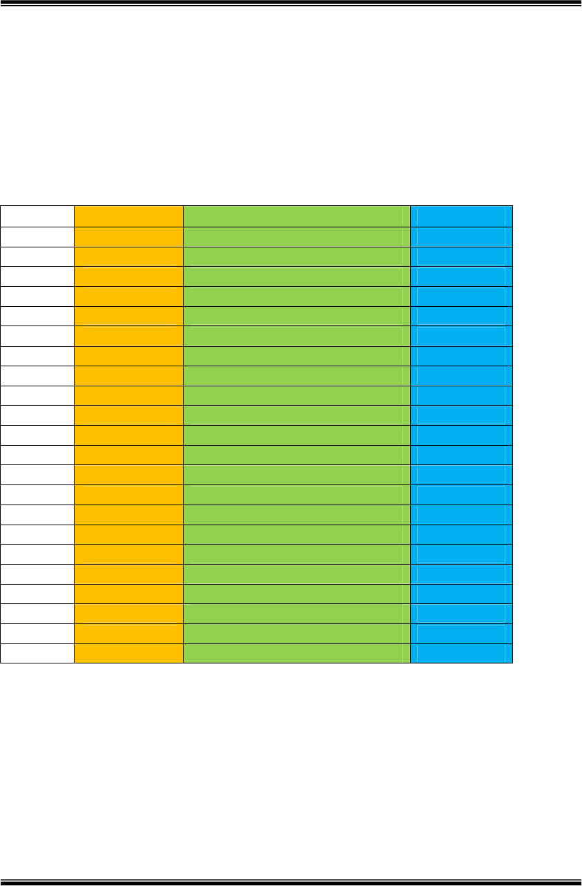
Table 2 GPIO Function Mapping
Mbist ModePerial Mode GPIO Mode
GPIO0Mbist DoneUART2_TXD/I2C2_SCLGeneral I/O
GPIO1Mbist_FailUART2_RXD/I2C2_SDAGeneral I/O
GPIO2inputpcm2_clk/TXENGeneral I/O
GPIO3inputpcm2_sync/RXENGeneral I/O
GPIO4inputpcm2_din/UART1_TX_MonitorGeneral I/O
GPIO5inputpcm2_dout/UART1_RX_MonitorGeneral I/O
GPIO6inputpcm2_codec_clk/spi_csnGeneral I/O
GPIO7inputspi_sckGeneral I/O
GPIO8inputspi_mosiGeneral I/O
GPIO9inputspi_misoGeneral I/O
GPIO10inputPWM0General I/O
GPIO11Mbist_PassPWM1General I/O
GPIO12inputsd_clk/clk13mGeneral I/O
GPIO13inputsd_cmd/SCLGeneral I/O
GPIO14inputsd_data[0]/SDAGeneral I/O
GPIO15inputsd_data[1]General I/O
GPIO16inputsd_data[2]General I/O
GPIO17inputsd_data[3]General I/O
GPIO18Mbist_Fail_BT
jtag_TCK
General I/O
GPIO19dram_result[2]
jtag_TMS
General I/O
GPIO20dram_result[1]
jtag_TDI
General I/O
GPIO21dram_result[0]
jtag_TDO
General I/O
All GPIO can be source to wake up MCU from shut down state. In shut down state, any level change on the set GPIO will trigger the wake up procedure.
When power on, the default state of GPIO0~GPIO9 and GPIO12~GPIO20 is high impedance and pull low internally; the default state of GPIO10~GPIO11 is high impedance and pull high; and the default state of GPIO21 is high impedance only.

Low Power Bluetooth Audio SoC
Page 7 of 14
3.2.PWM Timer and Watch Dog Timer
There are two sets of PWM timers. One fast set uses 1 MHz clock as main clock, and another slow set uses 32 kHz clock as main clock. Each set has three 16 bits counter with 4 bit pre-divider. First two timers in slow set can be used to LED duty cycle control.
The watch dog timer runs with 32 kHz clock, with period from 0.6 ms to 38 second.
3.3.Power Management
The BK8000L supports USB power supply thatit can work without battery. When there is a USB power supply, it will charge the battery with automatically charge current control while provide power to the BK8000L. The buck will give nearly half current reduction for digital power.
The BK8000L can enter into shut down mode when there is no active connection. The shut mode can be waked up by GPIO and USB charge.
3.4.MCU
The 16 bit RISC MCU has 16 KB I-Cache and DMA bus, to support efficient execution and frequently data exchange. The JTAG interface can be used to on- line debug, which can be also configured as GPIO.
Besides 26 MHz crystal, the MCU can run with internal programmable ROSC clock, or 32 kHz ring oscillator clock, with programmable divided ratio.
3.5.I2C and UART Interface
There is one set of I2C interface and one set of UART interface for debug or external MCU control the BK8000L. They share the two same GPIO0 and GPIO1.
3.6.FM Receiver Control Interface

BK8000L Datasheet
Page 8 of 14
The FM receiver control interface consists of a two-wire I2C interface and a 13 MHz clock for FM receiver reference.
3.7.FLASH Access Interface
The BK8000L MCU is running with the external FLASH program memory and the internal instruction cache. The external FLASH can be also used to store user data such as key configuration and Bluetooth paring information.
3.8.SPI
The 4-wires SPI supports high speed data communication, which can be used as interface to either external FLASH or LCD controller.
3.9.SAR ADC and LED
The SAR ADC has 10-bit resolution, and the two LED drivers support up to 10 mA current.
The SAR has six active channel as follows.
Table 3 ADC Channel Table
Channel Number
Detected VoltageDescription
1VBAT-pin/4Battery voltage 2VADC-pinPin VADC voltage 3Charge current detector
Used to detect charge current and charge circuit control 4VCC5USB-pin/6USB voltage 5GPIO19GPIO19 voltage 6GPIO9GPIO9 voltage
3.10.Audio Peripheral
There are one set of speech ADC with sample rate 8 kHz or 16 kHz, 44.1 kHz or 48 kHz. The DAC have two channels for stereo application, with sample rate 8 kHz, 16 kHz, 44.1 kHz or 48 kHz.
Low Power Bluetooth Audio SoC
Page 9 of 14
There is also a stereo line in interface, to allow external stereo input passing internal 31 dB programmable gain amplify to stereo output.
4.Electrical Characteristics
4.1.Absolute Maximum Ratings
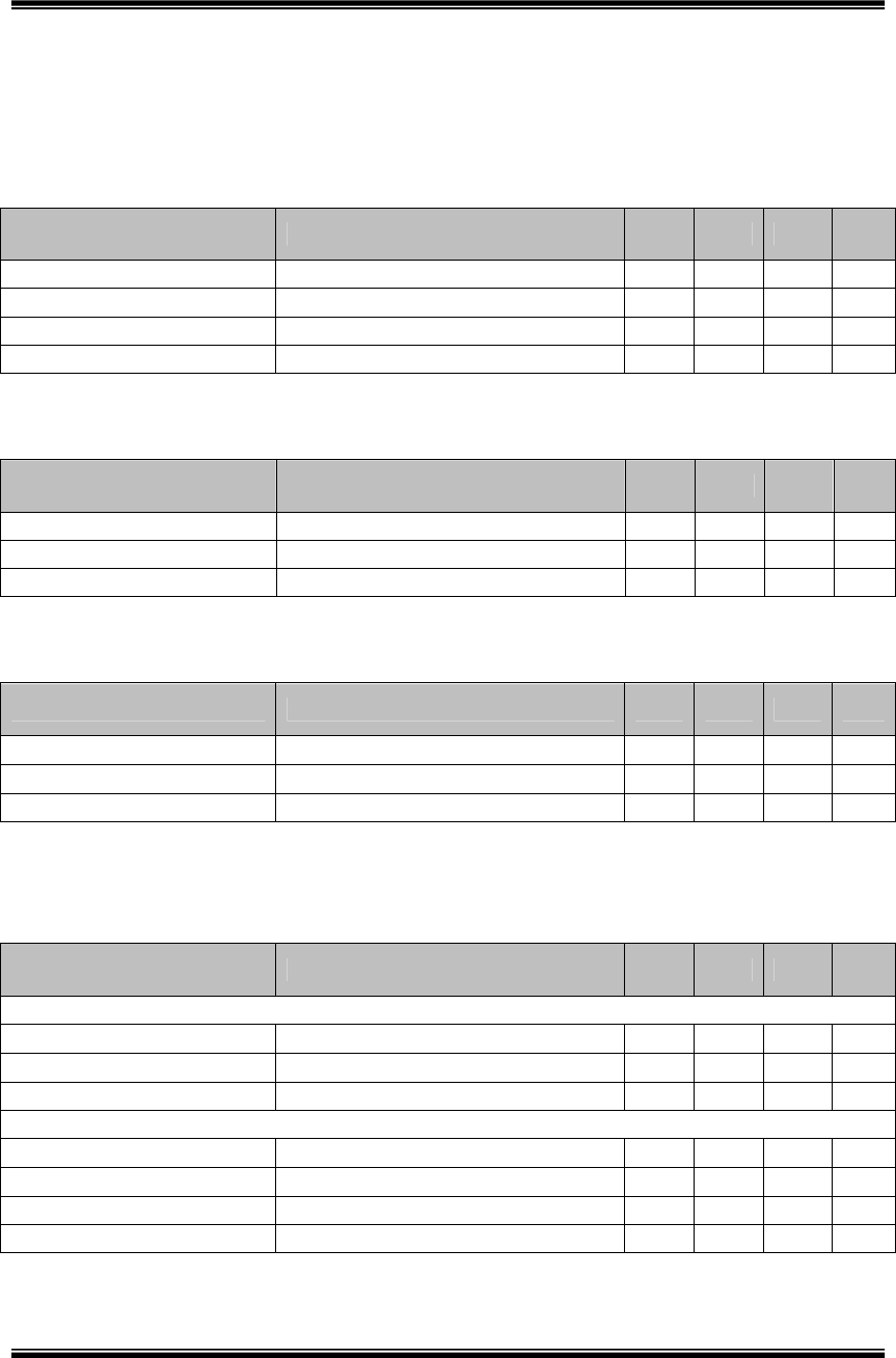
ParameterDescriptionMINTYPMAXUnit
VCCBATBattery regulator Supply voltage-0.33.34.2V
PRX
RX input power-10-dBm
TSTR
Storage temperature range-40-150℃VCCIOIO interface voltage-0.32.83.6V
4.2.Recommended Operating Conditions
ParameterDescriptionMINTYPMAXUnit
VCCBATBattery regulator Supply voltage2.83.34.2V
TOPR
Operation temperature range-20-80℃VCCIOIO interface voltage1.8-4.2V
4.3.System LDO
StateDescriptionMINTYPMAXUnit
VCC4BATVBAT2.84.2
VVCC3SYSSYSLDO Output Voltage2.83.63.8
VLoad CurrentLoading Current150mA
4.4.Analog LDO/BUCK
System can choose the analog BUCK or LDO as the power supply of RF and Audio part.
StateDescriptionMINTYPMAXUnit
Analog LDO
VCC3BUCKAAnalog LDO Input Voltage2.83.33.6
VVBUCKAAnalog LDO Output Voltage1.71.82.4
VLoad CurrentLoading Current100mA
Analog BUCK
VCC3BUCKAAnalog BUCK Input Voltage2.83.33.6
VVBUCKAAnalog BUCK Output Voltage1.71.82.4
VLoad CurrentLoading Current100mA
Switching frequencyBUCK modulation frequency2510MHz
BK8000L Datasheet
Page 10 of 14
4.5.Digital LDO/BUCK
System can also choose the digital BUCK or LDO as the power supply for the Digital part.
StateDescriptionMINTYPMAXUnit
Digital LDO
VSYS3V8DDigital LDO Input Voltage2.83.33.6
VVBUCKDDigital LDO Output Voltage1.21.35
VLoad CurrentLoading Current100mA
Digital BUCK
VSYS3V8DDigital BUCK Input Voltage2.83.33.6
VVBUCKDDigital BUCK Output Voltage1.21.35
VLoad CurrentLoading Current100mA
Switching frequencyBUCK modulation frequency2510MHz
4.6.USB LDO
When USB is plug in, VCC3SYS will be generated from USB LDO.
StateDescriptionMINTYPMAXUnit
VCC5USBUSB Input Voltage4.7555.75
VVCC3SYSUSBLDO Output Voltage3.3
VLoad CurrentLoading Current100mA
4.7.Typical Power Consumption
StateDescriptionMINTYPMAXUnit
Shut down
Software shut down, wake up from GPIO
50uA
Idle-SniffIdle state at Sniff mode900uA
Active(A2DP)2DH520mA
Active (HFP)HV120mA
4.8.RF Characteristics
ParameterConditionMINTYPMAXUnit
Operate Frequency2402~248024022480MHz
RXSENS-1 MbpsBER=0.001-90dBm
RXSENS-2 MbpsBER=0.0001-92dBm
RXSENS-3 MbpsBER=0.0001-84dBm
Maximum received signalBER=0.0010dBm
Maximum RF transmit power
5dBm
RF Power Control Range30dB

Low Power Bluetooth Audio SoC
Page 11 of 14
4.9.Audio Characteristics
ParameterConditionMINTYPMAXUnit
DAC Output Amplitude1Vrms
DAC output SNR1 kHz sine wave96dB
DAC Sample Rate848kHz
ADC SNR1 kHz sine wave96dB
ADC Sample Rate848kHz
5.Application Schematic
It will be provided with separatedocument.
6.About the Qualification
By carefully PCB layout, the BK8000L RFperformance meets FCC, CE and BQB requirement. The Bluetooth protocol and profile provided by Beken are already qualified and listed in SIG website. If there is any end product listing requirement with the BK8000L, please inquire Beken for the related QDID authorization.
BK8000L Datasheet
Page 12 of 14
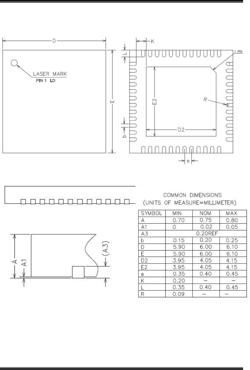
7.Package Information
The BK8000Luses the QFN 6x6 48-Pin package.

Low Power Bluetooth Audio SoC
Page 13 of 14
8.Ordering Information
Part numberPackagePackingMOQ (ea)
BK8000LQBQFN6mmx6mm48-PinTape Reel10 k
Remark:
MOQ: Minimum Order Quantity

NOTE: This equipment has been tested and found to comply with the limits for a Class B digital
device, pursuant to part 15 of the FCC Rules. These limits are designed to provide reasonable protection
against harmful interference in a residential installation. This equipment generates, uses and can radiate
radio frequency energy and, if not installed and used in accordance with the instructions, may cause
harmful interference to radio communications. However, there is no guarantee that interference will not
occur in a particular installation. If this equipment does cause harmful interference to radio or television
reception, which can be determined by turning the equipment off and on, the user is encouraged to try to
correct the interference by one or more of the following measures:
—Reorient or relocate the receiving antenna.
—Increase the separation between the equipment and receiver.
—Connect the equipment into an outlet on a circuit different from that to which the receiver is
connected.
—Consult the dealer or an experienced radio/TV technician for help.
Attention:LimitedModularApproval‐thisRFModulemaynotbesoldtothegenericpublic
andrequiresprofessionalinstallation.
DuetothefactthatthisRFModuleisnotequippedwithanownshielding,theend‐product
incl.thisRFModulehastoshowcompliancetotheFCCrules(15C/radiatedemissions).
(OEM)Integratorhastoassurecomplianceoftheentireend‐product
incl.theintegratedRFModule.Additionalmeasurements(15C)and/orequipmentauthorizations
(e.g
mayneedtobeaddresseddependingonco‐locationorsimultaenous
transmissionissuesifapplicable.
Integratorisremindedtoassurethattheseinstallationinstructions
willnotbemadeavailabletotheend‐userofthefinalhostdevice.
integratedintoany(portable,mobile,fixed)hostdevice.
Thefinalhostdevice,intowhichthisRFModuleisintegrated"hastobelabelled
withanauxilliarylablestatingtheFCCIDoftheRFModule,suchas
"ContainsFCCID:
Dependingonthesizeofthefinalend‐product,the§15.19FCCstatement
"Thisdevicecomplieswithpart15oftheFCCrules.Operationissubjecttothefollowingtwo
conditions:
(1)thisdevicemaynotcauseharmfulinterference,and
(2)thisdevicemustacceptanyinterferencereceived,including
interferencethatmaycauseundesiredoperation."
shouldbeplacedalsoonthedeviceoralternativelywithinaprominentlocationoftheusers
manual
The§15.21"Changes or modifications to this unit not expressly
approvedbythepartyresponsibleforcompliancecould
voidtheuser’sauthoritytooperatetheequipment."statementhastobeincludedinaprominent
locationoftheusersmanual
".
2AG94F-6688
)
either a complete new certification or a Class II Permissive Change.
the Integrator will be responsible to satisfy SAR/ RF Exposure requirements,
when the module