Sierra Wireless AR7584 Wireless Module User Manual Hardware Integration Guide
Sierra Wireless Inc. Wireless Module Hardware Integration Guide
AirPrime - AR7584 - Hardware Integration Guide

4111xxxx
0.1
Nov 06, 2017
AirPrime AR7584
Hardware Integration Guide

41110461XXXX Rev 0.1 January 16, 2017 2
Hardware Integration Guide
Important Notice
Due to the nature of wireless communications, transmission and reception of data can never be
guaranteed. Data may be delayed, corrupted (i.e., have errors) or be totally lost. Although significant
delays or losses of data are rare when wireless devices such as the Sierra Wireless modem are used
in a normal manner with a well-constructed network, the Sierra Wireless modem should not be used
in situations where failure to transmit or receive data could result in damage of any kind to the user or
any other party, including but not limited to personal injury, death, or loss of property. Sierra Wireless
accepts no responsibility for damages of any kind resulting from delays or errors in data transmitted or
received using the Sierra Wireless modem, or for failure of the Sierra Wireless modem to transmit or
receive such data.
Safety and Hazards
Do not operate the Sierra Wireless modem in areas where cellular modems are not advised without
proper device certifications. These areas include environments where cellular radio can interfere such
as explosive atmospheres, medical equipment, or any other equipment which may be susceptible to
any form of radio interference. The Sierra Wireless modem can transmit signals that could interfere
with this equipment. Do not operate the Sierra Wireless modem in any aircraft, whether the aircraft is
on the ground or in flight. In aircraft, the Sierra Wireless modem MUST BE POWERED OFF. When
operating, the Sierra Wireless modem can transmit signals that could interfere with various onboard
systems.
Note: Some airlines may permit the use of cellular phones while the aircraft is on the ground and the door
is open. Sierra Wireless modems may be used at this time.
The driver or operator of any vehicle should not operate the Sierra Wireless modem while in control of
a vehicle. Doing so will detract from the driver or operator’s control and operation of that vehicle. In
some states and provinces, operating such communications devices while in control of a vehicle is an
offence.
Limitations of Liability
This manual is provided “as is”. Sierra Wireless makes no warranties of any kind, either expressed or
implied, including any implied warranties of merchantability, fitness for a particular purpose, or
noninfringement. The recipient of the manual shall endorse all risks arising from its use.
The information in this manual is subject to change without notice and does not represent a
commitment on the part of Sierra Wireless. SIERRA WIRELESS AND ITS AFFILIATES
SPECIFICALLY DISCLAIM LIABILITY FOR ANY AND ALL DIRECT, INDIRECT, SPECIAL,
GENERAL, INCIDENTAL, CONSEQUENTIAL, PUNITIVE OR EXEMPLARY DAMAGES INCLUDING,
BUT NOT LIMITED TO, LOSS OF PROFITS OR REVENUE OR ANTICIPATED PROFITS OR
REVENUE ARISING OUT OF THE USE OR INABILITY TO USE ANY SIERRA WIRELESS
PRODUCT, EVEN IF SIERRA WIRELESS AND/OR ITS AFFILIATES HAS BEEN ADVISED OF THE
POSSIBILITY OF SUCH DAMAGES OR THEY ARE FORESEEABLE OR FOR CLAIMS BY ANY
THIRD PARTY.
Notwithstanding the foregoing, in no event shall Sierra Wireless and/or its affiliates aggregate liability
arising under or in connection with the Sierra Wireless product, regardless of the number of events,
occurrences, or claims giving rise to liability, be in excess of the price paid by the purchaser for the
Sierra Wireless product.
41110461XXXX Rev 0.1 January 16, 2017 3
Hardware Integration Guide
Patents
This product may contain technology developed by or for Sierra Wireless Inc.
This product includes technology licensed from QUALCOMM®.
This product is manufactured or sold by Sierra Wireless Inc. or its affiliates under one or more patents
licensed from InterDigital Group and MMP Portfolio Licensing.
Copyright
© 2016 Sierra Wireless. All rights reserved.
Trademarks
Sierra Wireless®, AirPrime®, AirLink®, AirVantage®, WISMO®, ALEOS® and the Sierra Wireless and
Open AT logos are registered trademarks of Sierra Wireless, Inc. or one of its subsidiaries.
Watcher® is a registered trademark of Netgear, Inc., used under license.
Windows® and Windows Vista® are registered trademarks of Microsoft Corporation.
Macintosh® and Mac OS X® are registered trademarks of Apple Inc., registered in the U.S. and other
countries.
QUALCOMM® is a registered trademark of QUALCOMM Incorporated. Used under license.
Other trademarks are the property of their respective owners.
Contact Information
Sales information and technical support,
including warranty and returns
Web: sierrawireless.com/company/contact-us/
Global toll-free number: 1-877-687-7795
6:00 am to 6:00 pm PST
Corporate and product information
Web: sierrawireless.com

41110461XXXX Rev 0.1 January 16, 2017 4
Hardware Integration Guide
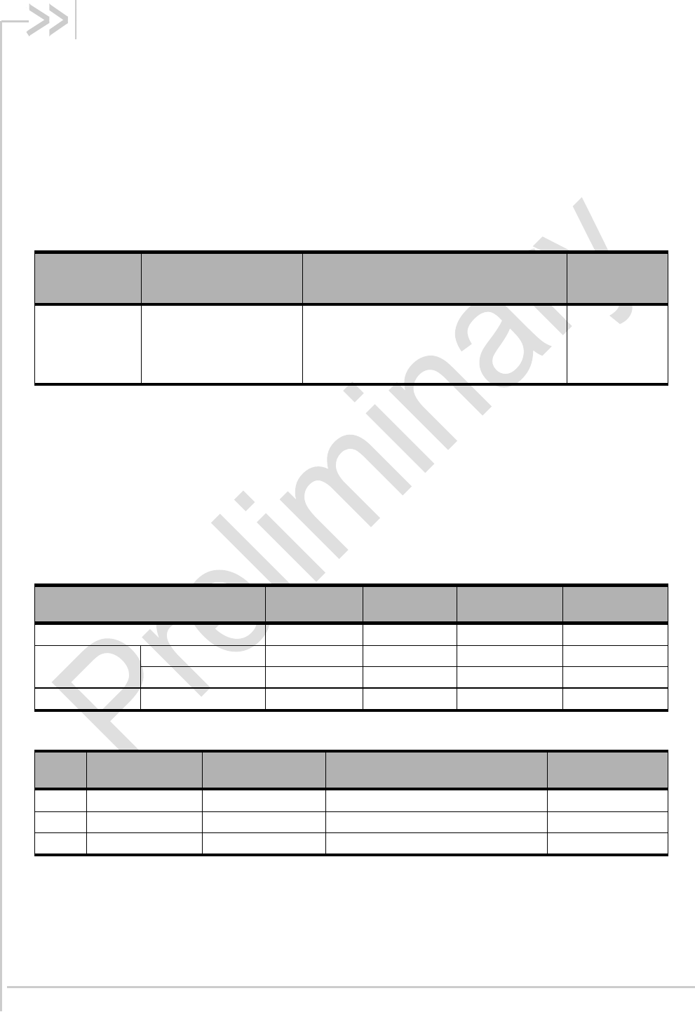
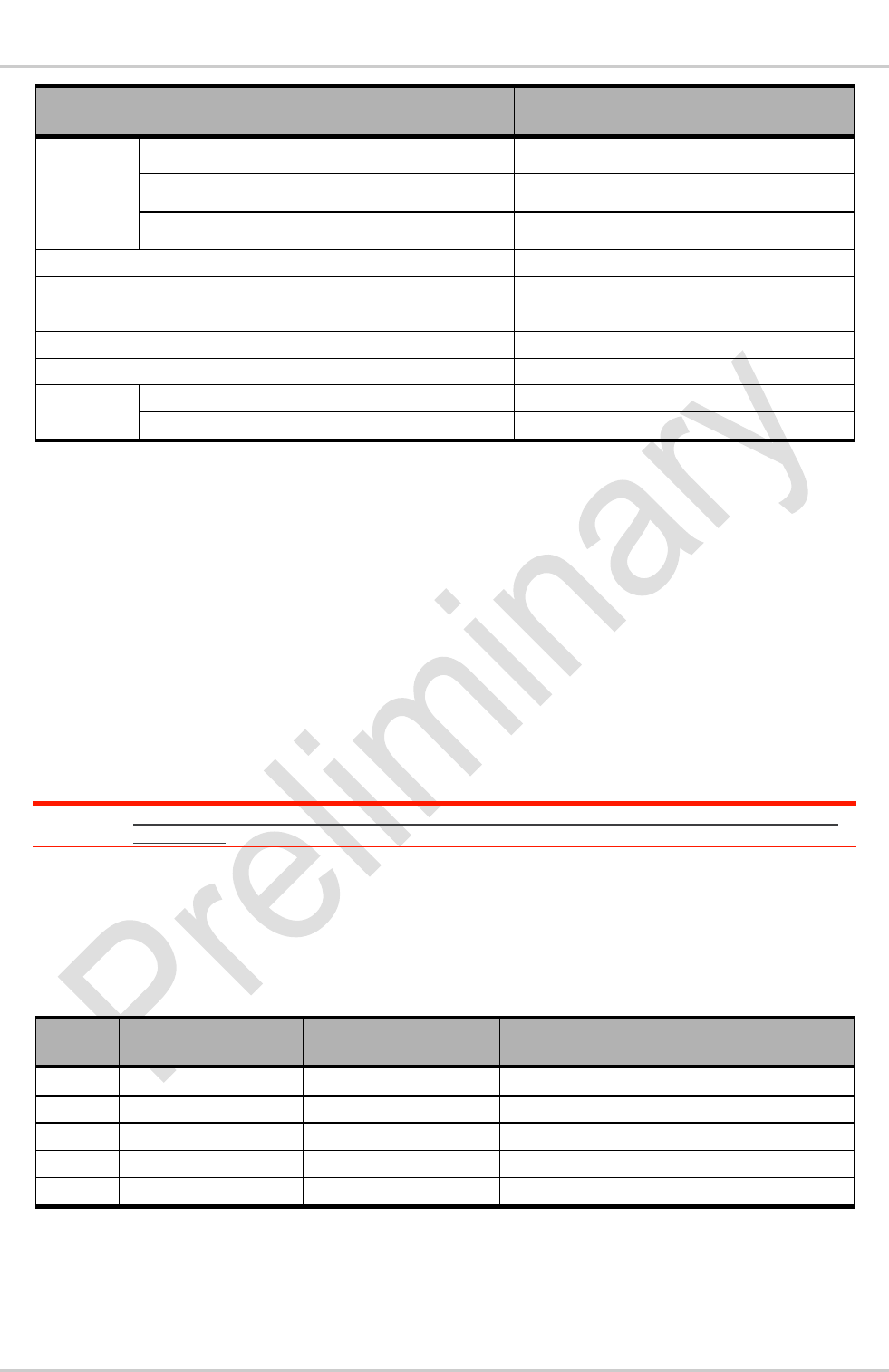
Document History
Version
Date
Updates
0.1
Nov 06, 20167
Creation

41110461 Rev 0.1 January 16, 2017 5
Contents
1. INTRODUCTION .................................................................................................. 9
1.1. General Features .............................................................................................................. 9
1.2. Power ................................................................................................................................ 9
1.3. RF ...................................................................................................................................... 9
1.3.1. GSM RF Interface .................................................................................................... 10
1.3.1.1. GSM TX Output Power.................................................................................................. 10
1.3.1.2. GSM RX Sensitivity ....................................................................................................... 10
1.3.2. WCDMA RF Interface .............................................................................................. 11
1.3.2.1. WCDMA TX Output Power ............................................................................................ 11
1.3.2.2. WCDMA RX Sensitivity ................................................................................................. 11
1.3.3. LTE RF Interface ...................................................................................................... 12
1.3.3.1. LTE TX Output Power ................................................................................................... 12
1.3.3.2. LTE RX Sensitivity ........................................................................................................ 12
1.3.4. WWAN Antenna Interface ........................................................................................ 13
1.3.4.1. WWAN Antenna Recommendations ............................................................................. 14
1.4. GNSS .............................................................................................................................. 15
1.4.1. GNSS Receiver ........................................................................................................ 15
1.4.2. GNSS Antenna Interface .......................................................................................... 16
1.4.2.1. GNSS Antenna Recommendations ............................................................................... 16
1.5. Electrical Specifications ................................................................................................... 17
1.5.1. Absolute Maximum Ratings ..................................................................................... 17
1.5.2. Digital IO Characteristics .......................................................................................... 17
2. AUDIO SPECIFICATION .................................................................................... 20
2.1. Digital Audio .................................................................................................................... 20
3. ROUTING CONSTRAINTS AND RECOMMENDATIONS ................................. 21
3.1. RF Routing Recommendations ....................................................................................... 21
3.2. USB Routing Recommendations ..................................................................................... 23
3.3. Power and Ground Recommendations ........................................................................... 23
3.4. Antenna Recommendations ............................................................................................ 24
3.5. Interface Circuit Recommendations ................................................................................ 24
4. FIRMWARE AND TOOLS .................................................................................. 25
4.1. Modem Firmware............................................................................................................. 25
4.2. Tools ................................................................................................................................ 25
5. APPROVAL ........................................................................................................ 26
5.1. Important Notice .............................................................................................................. 26
5.2. Safety and Hazards ......................................................................................................... 26
5.3. Important Compliance Information .................................................................................. 26
5.4. IC Regulations ................................................................................................................. 27
5.4.1. Radiation Exposure Statement ................................................................................ 27
6. REFERENCES ................................................................................................... 28


41110461 Rev 0.1 January 16, 2017 7
List of Figures
Figure 1. AppCAD Screenshot for Microstrip Design Power Mode Diagram ................................. 21
Figure 2. RF Routing Examples ..................................................................................................... 22
Figure 3. Coplanar Clearance Example ......................................................................................... 22
Figure 4. Antenna Microstrip Routing Example .............................................................................. 23
Figure 5. AirPrime AR758x Series Interface Reference Circuit...................................................... 24

41110461 Rev 0.1 January 16, 2017 8
List of Tables
Table 1. AirPrime AR758x Series Embedded Modules .................................................................. 9
Table 2. AirPrime AR758x Series Supported Carrier Aggregation Combinations1 ......................... 9
Table 3. Power Supply Requirements ............................................................................................. 9
Table 4. Power Supply Pads ........................................................................................................... 9
Table 5. Conducted TX (Transmit) Max output Power Tolerances – GSM/EDGE Bands ............ 10
Table 6. Conducted RX (Receive) Sensitivity – GSM/EDGE Bands ............................................ 10
Table 7. Conducted TX (Transmit) Max output Power Tolerances – WCDMA Bands ................. 11
Table 8. Conducted Primary RX (Receive) Sensitivity – UMTS Bands1 ....................................... 11
Table 9. Conducted Secondary RX (Receive) Sensitivity – UMTS Bands1 .................................. 11
Table 10. Conducted TX (Transmit) Max output Power Tolerances – LTE Bands ......................... 12
Table 11. Conducted RX Sensitivity 3GPP (BW: 10MHz) – LTE Bands1, 4..................................... 13
Table 12. Conducted RX Sensitivity SISO (BW: 10MHz) – LTE Bands1 ........................................ 13
Table 13. WWAN Antenna Interface Pads ...................................................................................... 13
Table 14. AirPrime AR758x Series WWAN Antenna Recommendations ....................................... 14
Table 15. GNSS Specifications ....................................................................................................... 15
Table 16. GNSS Antenna Interface Pads ........................................................................................ 16
Table 17. AirPrime AR758x Series Absolute Maximum Ratings..................................................... 17
Table 18. Digital IO Characteristics for VCC=1.8V Nominal ........................................................... 17
Table 19. Digital IO Characteristics for SDIO VCC=1.8V Nominal ................................................. 18
Table 20. Digital IO Characteristics for SDIO VCC=2.85V Nominal ............................................... 18
Table 21. Digital IO Characteristics for UICC_VCC=1.8V Nominal ................................................ 19
Table 22. Digital IO Characteristics for UICC_VCC=2.85V Nominal .............................................. 19
Table 23. Digital Audio Interface Pads1 ........................................................................................... 20
Table 24. Approved Antenna Types ................................................................................................ 27
Table 25. Reference Specifications ................................................................................................. 28
Table 26. Abbreviations ................................................................................................................... 29
41110461 Rev 0.1 January 16, 2017 9
1. Introduction
1.1. General Features
The AirPrime AR7584 embedded modules are designed for the automotive industry. It support LTE,
WCDMA and GSM air interface standards. It also have Global Navigation Satellite System (GNSS)
capabilities including GPS, GLONASS, Galileo, BeiDou, and QZSS
The AirPrime AR7584 embedded modules are based on the Qualcomm MDM9628 wireless chipset
and support the following bands.
Table 1. AirPrime AR758x Series Embedded Modules
Product
Description
Band Support
Target
Region1
AR7584
LTE / WCDMA / GSM /
GPRS / EDGE embedded
module
LTE: B1, B3, B7, B8, B20, B28A*
WCDMA: B1, B3, B8
GSM/GPRS/EDGE: 900/1800
EMEA
(Europe,
Middle East)
1 Other regions or operators which use the same frequency bands may also be supported, subject to review and
confirmation by Sierra Wireless.
* Optional band
1.2. Power
The AirPrime AR7584 are powered via a single regulated DC power supply, 3.7V nominal.
Table 2. Power Supply Requirements
Power Supply
Min
Typ
Max
Units
Main DC Power Input Range (VBATT)
3.4
3.7
4.2
V
Power Supply
Ripple
0 to 1kHz
-
-
200
mVpp
>1kHz
-
-
50
mVpp
Peak Current
AR758x
-
2000
3000
mA
Table 3. Power Supply Pads
Pad
Name
Direction
Function
If Unused
EA2
VBATT
Input
Power Supply Input
Must Be Used
EB2
VBATT
Input
Power Supply Input
Must Be Used
EC2
VBATT
Input
Power Supply Input
Must Be Used
1.3. RF
This section presents the WWAN RF interface of the AirPrime AR7584. The specifications for the
LTE, GSM and WCDMA interfaces are defined.
41110461XXXX Rev 0.1 January 16, 2017 10
Hardware Integration Guide
Introduction
1.3.1. GSM RF Interface
This section presents the GSM RF Specification for the AirPrime AR7584.
1.3.1.1. GSM TX Output Power
The GSM Maximum Transmitter Output Power of the AirPrime AR7584 are specified in the following
table.
Note: All values presented in the table below are preliminary.
Table 4. Conducted TX (Transmit) Max output Power Tolerances – GSM/EDGE Bands
Band
Standard 1
(dBm)1
Standard 2
(dBm)2
TX Power @
Room (dBm)
TX Power @
Class A (dBm)3
Notes
EGSM 900
33± 2dB
33± 2.5dB
33± 2dB
33± 2.5dB
GMSK mode,
connectorized(Class
4; 2 W, 33 dBm)
GSM 1800
30± 2dB
30± 2.5dB
30± 2dB
30± 2.5dB
GMSK mode,
connectorized(Class
1; 1 W, 30 dBm)
EGSM 900
27± 3dB
27± 4dB
27± 2.5dB
27± 3.5dB
8PSK mode,
connectorized(Class
E2; 0.5 W, 27 dBm)
GSM 1800
26± 3dB
26± 4dB
26 ± 2.5dB
26± 3.5dB
8PSK mode,
connectorized(Class
E2; 0.4 W, 26 dBm)
1 Per 3GPP TS 51.010-1 Requirement for Normal condition.
2 Per 3GPP TS 51.010-1 Requirement for Extreme conditions
3 Test at Class A extreme condition
1.3.1.2. GSM RX Sensitivity
The GSM Receiver Sensitivities of the AirPrime AR758x Series are specified in the following table.
Table 5. Conducted RX (Receive) Sensitivity – GSM/EDGE Bands
GSM/EDGE Bands
Limit
(dBm)1
Room
Typical
(dBm)
Class A
(Extrem
e)
Typical
(dBm)2
Class
A
Limit
(dBm)
EGSM 900
2% BER CS
CS
-102
-109
-108
-103
10% BLER
GMSK CS1
-104
-108
-107
-105
10% BLER
EDGE MCS5
-98
-103.5
-102
-99
DCS 1800
2% BER CS
CS
-102
-109
-108
-103
10% BLER
GMSK CS1
-104
-108.5
-107.5
-105
10% BLER
EDGE MCS5
-98
-103
-102
-99
1 Per 3GPP specification
2 Test at Class A extreme condition
41110461XXXX Rev 0.1 January 16, 2017 11
Hardware Integration Guide
Introduction
1.3.2. WCDMA RF Interface
This section presents the WCDMA RF Specification for the AirPrime AR758x Series.
1.3.2.1. WCDMA TX Output Power
The WCDMA Maximum Transmitter Output Power of the AirPrime AR758x Series is specified in the
following table.
Note: All values presented in the table below are preliminary.
Table 6. Conducted TX (Transmit) Max output Power Tolerances – WCDMA Bands
Band1
Limit (dBm)2
Room (dBm)
Class A (Extreme)
(dBm)3
B1
24 +1.7/-3.7dB
23.5 +2.2/-2.7dB
23.5 +2.2/-2.7dB
B3
24 +1.7/-3.7dB
23.5 +2.2/-2.7dB
23.5 +2.2/-2.7dB
B8
24 +1.7/-3.7dB
23.5 +2.2/-2.7dB
23.5 +2.2/-2.7dB
1 Connectorized (Class 3)
2 Per 3GPP TS 34.121-1 Specification
3 Test at Class A extreme condition
1.3.2.2. WCDMA RX Sensitivity
The WCDMA Receiver Sensitivities of the AirPrime AR758x Series are specified in the following table.
Table 7. Conducted Primary RX (Receive) Sensitivity – UMTS Bands1
Band
Limit (dBm)2
Room
Typical (dBm)
Class A
(Extreme) Typical
(dBm)3
Class A
Limit (dBm)
B2
-104.7
-109
Tbd
-105.5
B4
-106.7
-110
Tbd
-107.5
B5
-104.7
-110.5
Tbd
-105.5
B6
-106.7
-110.5
tbd
-107.5
1 1: CS 0.1% BER 12.2 kbps
2 Per 3GPP specification
3 Test at Class A extreme condition
Table 8. Conducted Secondary RX (Receive) Sensitivity – UMTS Bands1
Band
Room
Typical (dBm)
Class A (Extreme)
Typical (dBm)2
Class A
Limit ( dBm)
B1
-106.7
-110.5
-109
B3
-103.7
-111
-109.5
B8
-103.7
-111.5
-110.5
1 CS 0.1% BER 12.2 kbps
41110461XXXX Rev 0.1 January 16, 2017 12
Hardware Integration Guide
Introduction
2 Test at Class A extreme condition
1.3.3. LTE RF Interface
This section presents the LTE RF Specification for the AirPrime AR758x Series.
1.3.3.1. LTE TX Output Power
The LTE Maximum Transmitter Output Power of the AirPrime AR758x Series are specified in the
following table.
Note: The test configuration for all of the entries in the table below is per 3GPP specification,
Connectorized (Class 3).
Note: All values in the table below are preliminary.
Table 9. Conducted TX (Transmit) Max output Power Tolerances – LTE Bands
Band
Standard (dBm)
(Note 2)
Class A (dBm) (Note 3)
Notes
B1
23 ±2.7dB
23 ±2.2dB
Note 1
B3
23 ±2.7dB
23 ±2.2dB
Note 1, 4
B7
23 ±2.7dB
23 ±2.2dB
Note 1, 4
B8
23 ±2.7dB
23 ±2.2dB
Note 1, 4
B20
23 ±2.7dB
23 ±2.2dB
Note 1, 4
B28
23 ±2.7dB
23 ±2.2dB
Note 1
Note 1: The test configurations for all of the entries in the table above are per 3GPP specification, Connectorized (Class
3).
Note 2: Per 3GPP TS 36.521-1 6.2.2 UE Maximum Output Power ( No MPR);and for B13,Per VzW’s
Supplementary_RF_Conformance. 2.1 Maximum Output Power – No MPR Or A-MPR
Note 3: Class A is defined in 3.3 Environmental
Note 4: For transmission bandwidths (Figure 5.4.2-1 in 3GPP TS 36.521-1) confined within FUL_low and FUL_low + 4
MHz or FUL_high – 4 MHz and FUL_high, the maximum output power requirement is relaxed by reducing the lower
tolerance limit by 1.5 dB.
1.3.3.2. LTE RX Sensitivity
The LTE Receiver Sensitivities of the AirPrime AR758x Series are specified in the following table.
Note: For the table below:
Dual receiver (SIMO) per 3GPP TS 36.521-1 Rx Sensitivity Specification.
Sensitivity values scale with bandwidth:
x_MHz_Sensitivity = 10 MHz_Sensitivity – 10*log(10 MHz/x_MHz)
10 MHz BW,and 50 RB DownLink and Up Link RB configuration is as 3GPP TS 36.521-1 Table
7.3.5-2.
All values are preliminary pending transceiver matching and testing.
41110461XXXX Rev 0.1 January 16, 2017 13
Hardware Integration Guide
Introduction
Table 10. Conducted RX Sensitivity 3GPP (BW: 10MHz) – LTE Bands1, 4
Band
Standard
(dBm)2
Room Typical
(dBm)
Class A (Extreme)
Typical (dBm)5
Class A Limit
(dBm)5
B1
-96.3
-101
-100
-97
B3
-93.3
-101.5
-100
-94
B7
-94.3
-99.5
-98
-95
B8
-93.3
-102
-101.5
-94
B20
-93.3
-102
-101.5
-94
B28
-96.3
-102
-101
-95.5
1: Dual receiver (SIMO) per 3GPP TS 36.521-1 Rx Sensitivity Specification for Non-CA Configuration
2: Per 3GPP Specification.
3: Sensitivity values scale with bandwidth: x_MHz_Sensitivity = 10 MHz_Sensitivity – 10*log(10 MHz/x_MHz)
4: 10 MHz BW,and 50 RB DownLink and Up Link RB configuration is as 3GPP TS 36.521-1 Table 7.3.5-2.
5: Class A is defined in 3.3 Environmental
Note: For the table below:
Sensitivity values scale with bandwidth:
x_MHz_Sensitivity = 10 MHz_Sensitivity – 10*log(10 MHz/x_MHz)
10 MHz BW,and 50 RB DownLink and Up Link as 3GPP TS 36.521-1 Table 7.3.5-2.
All values are preliminary pending transceiver matching and testing.
Table 11. Conducted RX Sensitivity SISO (BW: 10MHz) – LTE Bands1
Band
Room Typical (dBm)
Class A (Extreme)Typical
(dBm)1
Class A Limit (dBm)1
Primary
Secondary
Primary
Secondary
Primary
Secondary
B1
-98
-98.5
-97
-97
-94
-94
B3
-98.5
-99
-97
-97.5
-91
-91
B7
--96
-96.5
-95
-95
-92
-92
B8
-98.5
-99.5
-98
-98.5
-91
-91
B20
-99.5
-99
-99
-98.5
-91
-91
B28
-99
-99.5
-98
-98.5
-92
-92
1: Class A is defined in 3.3 Environmental
1.3.4. WWAN Antenna Interface
The WWAN Antenna Interfaces of the AirPrime AR758x Series are defined in the table below.
Table 12. WWAN Antenna Interface Pads
Pad
Name
Direction
Function
BA11
GND
Primary Antenna Ground
BA12
PRIMARY_ANT
Input / Output
Primary Antenna Interface
BA13
GND
Primary Antenna Ground
BB11
GND
Primary Antenna Ground
41110461XXXX Rev 0.1 January 16, 2017 14
Hardware Integration Guide
Introduction
Pad
Name
Direction
Function
BB12
GND
Primary Antenna Ground
BA7
GND
Diversity Antenna Ground
BA8
DIVERSITY_ANT
Input
Diversity Antenna Interface
BA9
GND
Diversity Antenna Ground
BB7
GND
Diversity Antenna Ground
BB8
GND
Diversity Antenna Ground
1.3.4.1. WWAN Antenna Recommendations
The table below defines the key characteristics to consider for antenna selection.
Table 13. AirPrime AR758x Series WWAN Antenna Recommendations
Parameter
Requirements
Comments
Antenna system
External multi-band 2x2 MIMO
antenna system (Ant1/Ant2)a
Operating bands of
Ant1 and Ant2b
698–960 MHz
1451–1512 MHz
1710–1995 MHz
2110–2170 MHz
2500–2700 MHz
Operating bands depend on module’s
supported bands/modes
VSWR of Ant1 and
Ant2
1:1 (ideal)
< 2.5:1 (recommended)
On all bands including band edges
Total radiated
efficiency of Ant1 or
Ant2
> 50% on all bands
Measured at the RF connector.
Includes mismatch losses, losses in the
matching circuit, and antenna losses,
excluding cable loss.
Sierra Wireless recommends using
antenna efficiency as the primary
parameter for evaluating the antenna
system.
Peak gain is not a good indication of
antenna performance when integrated with
a host device (the antenna does not
provide omni-directional gain patterns).
Peak gain can be affected by antenna size,
location, design type, etc. — the antenna
gain patterns remain fixed unless one or
more of these parameters change.
Maximum antenna
gain
Must not exceed antenna gains due to
RF exposure and ERP/ EIRP limits,
as listed in the module’s FCC grant.
Isolation between
Ant1 and Ant2 (S21)
> 10 dB
If antennas can be moved, test all
positions for both antennas.
Unless otherwise specified, this
isolation requirement need to be
maintained for optimum operation.
Make sure all other wireless devices
(Bluetooth or WLAN antennas, etc.) are
turned OFF to avoid interference.
41110461XXXX Rev 0.1 January 16, 2017 15
Hardware Integration Guide
Introduction
Parameter
Requirements
Comments
Maximum Voltage
applied to antenna
36 Volts
Power handling
> 2 W RF power on low bands
> 1 W on high bands
Measure power endurance over 4
hours (estimated talk time) using a 2 W
CW signal — set the CW test signal
frequency to the middle of the PCS TX
band (1880 MHz for PCS).
Visually inspect device to ensure there
is no damage to the antenna structure
and matching components.
VSWR / TIS / TRP measurements
taken before and after this test must
show similar results.
* These worst-case VSWR figures for the transmitter bands may not guarantee RSE levels to be within regulatory limits.
The device alone meets all regulatory emissions limits when tested into a cabled (conducted) 50Ω system. With antenna
designs with up to 2.5:1 VSWR or worse, the radiated emissions could exceed limits. The antenna system may need to be
tuned in order to meet the RSE limits as the complex match between the module and antenna can cause unwanted levels
of emissions. Tuning may include antenna pattern changes, phase/delay adjustment, passive component matching.
Examples of the application test limits would be included in FCC Part 22, Part 24 and Part 27, test case 4.2.16 for GSM
(ETSI EN 301 511), and test case 4.2.2 for WCDMA (ETSI EN 301 908-1), where applicable.
a Ant1—Primary, Ant2—Diversity (Diversity/MIMO/)
b Stated band ranges satisfy requirements for both Ant1 and Ant2.
1.4. GNSS
The AirPrime AR758x Series include optional Global Navigation Satellite System (GNSS) capabilities
via the Qualcomm gpsOne Gen8C Engine, capable of operation in assisted and stand-alone modes
using GPS, GLONASS, Beidou, Galileo, and QZSS SVs.
Note: Galileo support pending system / satellite deployment.
1.4.1. GNSS Receiver
The table below summarizes the GNSS capabilities of the AirPrime AR758x Series.
Table 14. GNSS Specifications
Parameter/Feature
Value
Mode
GPS
L1
GLONASS (FDMA)
L1OF
Beidou
B1L
Galileo
E1
QZSS
L1
Satellite
channels
Tracking
40
Acquisition
118
Standalone
Time To
First Fix
(TTFF)
1,2,4,6
Hot start:
1 s
Warm start
27 s
Cold start
29 s
41110461XXXX Rev 0.1 January 16, 2017 16
Hardware Integration Guide
Introduction
Parameter/Feature
Value
Sensitivity
(GPS,
GLONASS,
BeiDou)
Tracking 4,5,6
-163 dBm
Cold start Acquisition
-158 dBm
Hot start Acquisition
-145 dBm
Horizontal Position accuracy 1,3,4,5,6,
2 / 57
Altitude accuracy 1,3,4,5,6,
4 / 107
Velocity accuracy 1,3,4,5,6
0.1
Tracking update rates
1 Hz
SBAS support 3
WAAS, EGNOS, MSAS,GAGAN
Message
Protocol
NMEA 0183 Version
V3.0
Supported Sentences
GSV, GNS, GSA, GGA, GRS, RMC, VTG
1 Open sky, all SV RF signal level = -130dBm, Number of GPS SVs > 6, Number of Glonass SVs>5, Number of Galileo
SVs>5, Number of BeiDou SVs>5
2 TTFF values show results in worst conditions (as an external host user): timing measurement start when GPS control
request is sent on AT command interface and stop when NMEA frames (1Hz update) display 2D fix information.
3 Scenarios used for accuracy measurements simulate car travel including direction, altitude and speed variations.
4 The performance are obtained by using external Pre-SAW and LNA for conducted test setup at Room temperature, it is
used to simulate the active antenna as customer’s application.
5 1Hz Navigation used for all tracking/navigation tests.
6 GNSS constellations used: GPS + GLONASS + Galileo + Beidou
7 Accuracy data are provided Circular Error Probable, CEP-50 / CEP-95. Means that 50%/95% of the positions returned
calculated have an error lower or equal to the accuracy value.
8 Tracking sensitivity is the lowest GNSS signal level for which the device can still detect an in-view satellite 50% of the
time when in sequential tracking mode..
9 Acquisition sensitivity is the lowest GNSS signal level for which the device can still detect an in-view satellite 50% of the
time.
Note: All GNSS characterization data are measured in conducted RF path with GNSS simulator at room
temperature.
1.4.2. GNSS Antenna Interface
The GNSS Antenna Interface is defined in the table below.
Table 15. GNSS Antenna Interface Pads
Pad
Name
Direction
Function
BA4
GND
GNSS Antenna Ground
BA5
GNSS_ANT
Input
GNSS Antenna Interface
BA6
GND
GNSS Antenna Ground
BB4
GND
GNSS Antenna Ground
BB5
GND
GNSS Antenna Ground
1.4.2.1. GNSS Antenna Recommendations
To be added in a future revision.
41110461XXXX Rev 0.1 January 16, 2017 17
Hardware Integration Guide
Introduction
1.5. Electrical Specifications
This section provides details of the key electrical specifications of the AirPrime AR758x Series.
1.5.1. Absolute Maximum Ratings
This section defines the Absolute Maximum Ratings of the AirPrime AR758x Series.
Warning: If operating outside of the defined specifications, even momentarily, damage may occur to the
device.
Table 16. AirPrime AR758x Series Absolute Maximum Ratings
Parameter
Min
Max
Units
VBATT
Power Supply Input
-
4.5
V
VIN
Voltage on any digital input or output pin
-
Vxx + 20%*
V
IIN
Latch-up current
-100
100
mA
ESD Ratings
ESD1
Primary, Secondary and GNSS antenna pads –
Contact
-
± 8
kV
All other signal pads – Contact
-
± 1.5
kV
1 The ESD Simulator configured with 150pF, 330Ω.
Caution: Vxx is the supply voltage associated with the input or output pin to which the test voltage is applied.
1.5.2. Digital IO Characteristics
The Digital IO characteristics are defined in the table below. These apply to GPIOs, UART, LED, SPI,
I2C, PCM/I2S, GNSS_LNA, WAKE_N, 2G_SYNC, AT_PORT_SW, SERVICE and RESET.
Table 17. Digital IO Characteristics for HSIC VDD=1.2V Nominal
Parameter
Comments
Min
Typ
Max
Units
VIH
High level input voltage
CMOS/Schmitt
0.78
–
1.44
V
VIL
Low level input voltage
CMOS/Schmitt
-0.3
–
0.42
V
IIH
Input high leakage current
No pull-down
–
–
2
µA
IIL
Input low leakage current
No pull-up
-2
–
–
µA
VOH
High-level output voltage
CMOS, at rated drive
strength
0.9
–
1.25
V
VOL
Low level output current
CMOS, at rated drive
strength
0
–
0.3
V
IZ
Tri-state leakage current
No pull, no keeper
-2
–
2
µA
CIN
Input capacitance
–
–
5
pF
41110461XXXX Rev 0.1 January 16, 2017 18
Hardware Integration Guide
Introduction
Table 18. The 1.8V Digital IO characteristics are defined in the table below. (Except SDIO1, UICC1 and UICC2/
Ethernet PHY Control interface)
Table 18. D Digital IO Characteristics for VDD=1.8V Nominal
Parameter
Comments
Min
Typ
Max
Units
VIH
High level input
voltage
CMOS/Schmitt
1.17
–
2.16
V
VIL
Low level input
voltage
CMOS/Schmitt
-0.3
–
0.63
V
VOH
High level
output voltage
CMOS, at pin rated
drive strength
1.35
–
1.93
V
VOL
Low-level
output voltage
CMOS, at pin rated
drive strength
0
–
0.45
V
VIH-PM
High level input
voltage
CMOS/Schmitt
1.17
–
2.1
V
VIL-PM
Low level input
voltage
CMOS/Schmitt
-0.3
–
0.63
V
VOH-PM
High level
output voltage
CMOS, at pin rated
drive strength
1.5
–
1.88
V
VOL-PM
Low-level
output voltage
CMOS, at pin rated
drive strength
0
–
0.3
V
IOH
High level
output current
VOH = 1.35 V
–
–
6
mA
IOL
Low Level
output current
VOL = 0.45 V
-6
–
–
mA
IOH-PM
High level
output current
GPIO_PMxx only
–
–
0.60
mA
IIHPD
Input high
leakage current
Logic High with pull-
down
5
33
µA
IILPU
Input low
leakage current
Logic Low with pull-up
-33
-5
µA
CIN
Input
capacitance
–
–
5
pF
Caution: Digital IOs shall not be pulled-up to an external voltage as this may cause VCC_1V8 to not go low
when the AirPrime AR758x/AR8582 device is powered down. Also, this would partially bias the
AirPrime AR758x/AR8582 device which could potentially damage the device or result in GPIOs
being set to undetermined levels.
Table 19. Digital IO Characteristics for SDIO1 VDD=1.8V Nominal
Parameter
Comments
Min
Typ
Max
Units
VIH
High level input voltage
CMOS/Schmitt
1.27
–
2
V
VIL
Low level input voltage
CMOS/Schmitt
-0.3
–
0.58
V
IIH
Input high leakage current
No pull-down
–
–
2
µA
IIL
Input low leakage current
No pull-up
-2
–
–
µA
VOH
High-level output voltage
CMOS, at rated drive strength
1.4
–
1.93
V
VOL
Low level output voltage
CMOS, at rated drive strength
0
–
0.45
V
41110461XXXX Rev 0.1 January 16, 2017 19
Hardware Integration Guide
Introduction
Table 20. Digital IO Characteristics for UICC_VCC1=3V/2.85V Nominal
Parameter
Comments
Min
Typ
Max
Units
VIH
High level input
voltage
CMOS/Schmitt
0.7* UICC_VCC
–
UICC_VCC + 0.3
V
VIL
Low level input
voltage
CMOS/Schmitt
-0.3
–
0.2* UICC_VCC
V
IIH
Input high
leakage current
No pull-down
–
–
10
µA
IIL
Input low
leakage current
No pull-up
-10
–
–
µA
VOH
High-level
output voltage
CMOS, at rated drive
strength
0.8* UICC_VCC
–
UICC_VCC
V
VOL
Low level
output current
CMOS, at rated drive
strength
0
–
0.4
V
Note 1: UICC2_VCC is 2.85V when Ethernet PHY Control interface is working.
41110461 Rev 0.1 January 16, 2017 20
2. Audio Specification
2.1. Digital Audio
The AirPrime AR758x Series provides two 4-wire digital audio interfaces. Each interface can be
configured as either a PCM or an I2S interface.
Table 21. Digital Audio Interface Pads1
Pad
Mode
Name
Direction2
Function
If Unused
DA3
PCM
PCM_CLK
Output
PCM Clock
Leave Open
I2S
I2S_SCLK
I2S Bit Clock
DB3
PCM
PCM_FS
Output
PCM Frame Sync
Leave Open
I2S
I2S_WS
I2S Word Select
DC2
PCM
PCM_DOUT
Output
PCM Data Out
Leave Open
I2S
I2S_DOUT
I2S Data Out
DD2
PCM
PCM_DIN
Input
PCM Data In
Leave Open
I2S
I2S_DIN
I2S Data In
DD3
PCM2
PCM_CLK
Output
PCM Clock
Leave Open
I2S2
I2S_SCLK
I2S Bit Clock
DD4
PCM2
PCM_FS
Output
PCM Frame Sync
Leave Open
I2S2
I2S_WS
I2S Word Select
DE2
PCM2
PCM_DOUT
Output
PCM Data Out
Leave Open
I2S2
I2S_DOUT
I2S Data Out
DC4
PCM2
PCM_DIN
Input
PCM Data In
Leave Open
I2S2
I2S_DIN
I2S Data In
1 PCM2/I2S2 is multiplexed with SPI2/UART3 and is not available if either SPI2/UART3 is configured
2 Direction when defined in Master mode.
41110461 Rev 0.1 January 16, 2017 21
3. Routing Constraints and
Recommendations
Layout and routing of the AirPrime AR758x Series in the application is critical to maintaining the
performance of the radio. The following sections provide guidance to the developer when designing
their application to include an AirPrime AR758x Series and achieve optimal system performance.
3.1. RF Routing Recommendations
To route the RF antenna signals, the following recommendations must be observed for PCB layout:
The RF signals must be routed using traces with a 50 characteristic impedance.
Basically, the characteristic impedance depends on the dielectric constant (εr) of the material used,
trace width (W), trace thickness (T), and height (H) between the trace and the reference ground plane.
In order to respect this constraint, Sierra Wireless recommends that a MicroStrip structure be used
and trace width be computed with a simulation tool (such as AppCAD, shown in the figure below and
available free of charge at http://www.avagotech.com).
Figure 1. AppCAD Screenshot for Microstrip Design Power Mode Diagram
The trace width should be wide enough to maintain reasonable insertion loss and manufacturing
reliability. Cutting out inner layers of ground under the trace will increase the effective substrate
height; therefore, increasing the width of the RF trace.
Caution: It is critical that no other signals (digital, analog, or supply) cross under the RF path. The figure
below shows a generic example of good and poor routing techniques.
41110461XXXX Rev 0.1 January 16, 2017 22
Hardware Integration Guide
Routing Constraints and Recommendations
Poor routing
Correct routing
The yellow traces cross the RF trace.
There is no signal around the RF path.
Figure 2. RF Routing Examples
Fill the area around the RF traces with ground and ground vias to connect inner ground layers
for isolation.
Cut out ground fill under RF signal pads to reduce stray capacitance losses.
Avoid routing RF traces with sharp corners. A smooth radius is recommended.
E.g. Use of 45° angles instead of 90°.
The ground reference plane should be a solid continuous plane under the trace.
The coplanar clearance (G, below) from the trace to the ground should be at least the trace
width (W) and at least twice the height (H). This reduces the parasitic capacitance, which
potentially alters the trace impedance and increases the losses.
E.g. If W = 100 microns then G = 200 microns in an ideal setup. G = 150 microns would also
be acceptable is space is limited.
Figure 3. Coplanar Clearance Example
Note: The figure above shows several internal ground layers cut out, which may not be necessary for
every application.

41110461XXXX Rev 0.1 January 16, 2017 23
Hardware Integration Guide
Routing Constraints and Recommendations
AR759x
RF Connector
GND
GND
GND
GND
GND
GND
ANT
50 Ohm Controlled Impedance Trace
2x Ground holdback – twice
the trace width
GND
GND
GND
GND
Figure 4. Antenna Microstrip Routing Example
3.2. USB Routing Recommendations
HighSpeed USB signals (USB_D_P / USB_D_M) are a differential pair and must be routed with the
following considerations/constraints:
90 Ohm differential +/- 10% trace impedance,
Differential trace length pair matching < 2mm (15 ps),
Solid reference planes,
Trace lengths < 120 mm,
And 2x the trace width separation to all adjacent signals.
SuperSpeed USB adds two differential pairs (SSRX+ / SSRX- and SSTX+ / SSTX-). These pairs
should be routed with the following considerations/constraints:
90 Ohm differential +/- 15% trace impedance,
Differential trace length pair matching < 0.7mm (5 ps),
Trace lengths < 112 mm,
And GND isolation from other adjacent traces with minimum of 2x the SSRX/SSTX trace
wdith.
3.3. Power and Ground Recommendations
Power and ground routing is critical to achieving optimal performance of the AirPrime AR758x Series
when integrated into an application.
Recommendations:
Do not use a separate GND for the Antennas.
Connections to GND from the AirPrime AR758x Series should be flooded plane using thermal
reliefs to ensure reliable solder joints.
VBATT is recommended to be routed as a wide trace(s) directly from the power supply to the
LGA pad.
41110461XXXX Rev 0.1 January 16, 2017 24
Hardware Integration Guide
Routing Constraints and Recommendations
3.4. Antenna Recommendations
Connecting the antenna ground reference to the vehicle chassis is not recommended since that has
been known to cause noise from the engine to couple into the audio of the device. It is ultimately up to
the integrator to evaluate this performance.
3.5. Interface Circuit Recommendations
The recommended interface implementation is to use a dual-supply bus transceiver with configurable
voltage translation. This allows a host processor operating at a different voltage to communicate with
the AirPrime AR758x Series using the appropriate voltage levels.
The figure below is a reference circuit for a digital input / output signal to / from the AirPrime AR758x
Series.
VCCA
VCCB DIR
AB GPIOx
VCC_1V8ApplVcc (1.2V – 3.6V)
ApplGPIOx
Direction
L = B to A
H = A to B
Figure 5. AirPrime AR758x Series Interface Reference Circuit
The dual-supply bus transceiver with configurable voltage translation used in the reference circuit
above is the Texas Instruments SN74AVC1T45.
If a Digital IO signal is used bidirectional in the application then a bidirectional level translator, such as
Texas Instruments TCA9406 is needed.

41110461 Rev 0.1 January 16, 2017 25
4. Firmware and Tools
The AirPrime AR7582 are designed based on Qualcomm’s MDM9628 chipset, which contains a
Modem Processor for running modem firmware components and an Application Processor for running
embedded Linux applications. Various tools are provided by Qualcomm and developed by Sierra
Wireless for developing and commercializing the AirPrime AR7584.
4.1. Modem Firmware
The MDM9628 Modem Process contains the following categories of firmware, with possible
modifications/extensions by Sierra Wireless as indicated:
LTE/ WCDMA/ TD-SCDMA air interface protocols
GNSS engine
IMS protocol stack
AT Command Processor: New AT commands will be added by Sierra Wireless. See
document [8] for the complete list of AT Commands for AR758x.
Data services
Drivers/ BSP: Some modifications will be made to ensure the firmware can communicate with
the AR758x module hardware properly.
UICC functions
Memory Management: Built-in redundancy and continuous monitoring against memory
corruption
Antenna Protection
Voice support
4.2. Tools
The following tools will be needed for the AirPrime AR7584 development, testing and
commercialization.
Firmware Update Tool
Linux driver and Application Downloader
Logging Tool
Qualcomm’s QXDM (license with Qualcomm required)
Qualcomm’s QPST (license with Qualcomm required)

41110461 Rev 0.1 January 16, 2017 26
5. Approval
5.1. Important Notice
Because of the nature of wireless communications, transmission and reception of data can never be
guaranteed. Data may be delayed, corrupted (i.e., have errors) or be totally lost.
Although significant delays or losses of data are rare when wireless devices such as the Sierra
Wireless modem are used in a normal manner with a well-constructed network, the Sierra Wireless
modem should not be used in situations where failure to transmit or receive data could result in
damage of any kind to the user or any other party, including but not limited to personal injury, death,
or loss of property. Sierra Wireless and its affiliates accept no responsibility for damages of any kind
resulting from delays or errors in data transmitted or received using Sierra Wireless modem, or for
failure of the Sierra Wireless modem to transmit or receive such data.
5.2. Safety and Hazards
Do not operate the AirPrime AR7584:
In areas where blasting is in progress
Where explosive atmospheres may be present including refueling points, fuel depots, and
chemical plants
Near medical equipment, life support equipment, or any equipment which may be susceptible
to any form of radio interference. In such areas, the AirPrime AR7584 device MUST BE
POWERED OFF. Otherwise, the AirPrime AR7584 device can transmit signals that could
interfere with this equipment
In an aircraft, the AirPrime AR7584 device MUST BE POWERED OFF. Otherwise, the
AirPrime AR7584 device can transmit signals that could interfere with various onboard
systems and may be dangerous to the operation of the aircraft or disrupt the cellular network.
Use of cellular phone in aircraft is illegal in some jurisdictions. Failure to observe this
instruction may lead to suspension or denial of cellular telephone services to the offender, or
legal action or both.
Some airlines may permit the use of cellular phones while the aircraft is on the ground and
the door is open. The AirPrime AR7584 device may be used normally at this time.
5.3. Important Compliance Information
The AirPrime AR7584 is granted with a modular approval for mobile applications. Integrators may use
the AR7584 device in their final products without additional FCC certification if they meet the following
conditions. Otherwise, additional FCC approvals must be obtained.
1. The end product must use the RF trace design approved with the AirPrime AR7584 module.
The Gerber file of the trace design can be obtained from Sierra Wireless upon request.
2. At least 20cm separation distance between the antenna and the user’s body must be
maintained at all times.
3. To comply with FCC regulations limiting both maximum RF output power and human
exposure to RF radiation, the maximum antenna gain including cable loss in a mobile-only
exposure condition must not exceed the gain values presented in the table below:
5.0 dBi in LTE Band 7
41110461XXXX Rev 0.1 January 16, 2017 27
Hardware Integration Guide
Approval
4. The AR7584 modem may transmit simultaneously with other collocated radio transmitters
within a host device, provided the following conditions are met:
Each collocated radio transmitter has been certfied by FCC for mobile application.
At least 20 cm separation distance between the antennas of the collocated transmitters
and the user’s body must be maintained at all times.
The output power and antenna gain must not exceed the limits and configu-rations
stipulated in the following table.
Device
Technology
Band
Frequency (MHz)
EIPR Limits
(dbm)
Maximum
antenna gain
AR7594
LTE
7
2500 – 2570
5
Collocated
transmitters*
WLAN
2400-2500
25
5150-580
27
WiMAX
2300-2400
25
2500-2700
25
3300-3800
25
BT
2400-2500
15
*. Valid collocated Transmitter combinations: WLAN+BT; WiMAX+BT. (WLAN+WiMAX+BT is not permitted.)
5. A label must be affixed to the outside of the end product into which the AirPrime AR7584
device is incorporated, with a statement similar to the following:
This device contains FCC ID: N7NAR7584
6. A user manual with the end product must clearly indicate the operating requirements and
conditions that must be observed to ensure compliance with current FCC RF exposure
guidelines.
The end product with an embedded AirPrime AR7584 device may also need to pass the FCC Part 15
unintentional emission testing requirements and be properly authorized.
Note: If this module is intended for use in a portable device, you are responsible for separate approval to
satisfy the SAR requirements of FCC Part 2.1093.
41110461XXX Rev 0.1 January 16, 2017 28
6. References
The table below lists the reference specifications for this product.
Table 22. Reference Specifications
Ref
Title
Rev
Issuer
[1]
3GPP TS 51.010-1
Version
7.3.1
3GPP
[2]
3GPP TS 34.121-1
V8
3GPP
[3]
3GPP TS 36.521-1
V9
3GPP
[4]
Universal Serial Bus Specification
V2.0
USB Implementers Forum
[5]
Universal Serial Bus CDC Subclass Specification for
Wireless Mobile Communication Devices
V1.0
USB Implementers Forum
[6]
Universal Serial Bus Class Definitions for
Communication Devices
V1.1
USB Implementers Forum
[7]
AirPrime - AR7 Series - Customer Process Guidelines
-
Sierra Wireless
[8]
AirPrime - AR75xx - AT Command Interface
Specification - 4112841
V1.5
Sierra Wireless
[9]
AirPrime AR7xxx Firmware Download Guide
-
Sierra Wireless
[10]
AirPrime AR758x Thermal Management Application
Note - 2174114
V1.0
Sierra Wireless
[11]
AirPrime AR758x Current Consumption Application
Note - 2174115
V1.0
Sierra Wireless
[12]
AirPrime - AR Series - Hardware Compatibility APN -
4116174
V0.8
Sierra Wireless
[13]
AirPrime - AR7552 - Hardware Integration Guide –
4117336
V1.0
Sierra Wireless

41110461XXX Rev 0.1 January 16, 2017 29
7. Abbreviations
The table below lists several abbreviations used in this document.
Table 23. Abbreviations
Abbreviation
Description
ADC
Analog-to-Digital Converter
CDMA
Code Division Multiple Access
DRX
Discontinuous Receive
EDGE
Enhanced Data rates for GSM Evolution
FDD
Frequency Division Duplex
GERAN
GSM EDGE Radio Access Network
GNSS
Global Navigation Satellite System
GSM
Global System for Mobile Communications
HSPA
High Speed Packet Access
I2S
Inter-IC Sound
LTE
Long Term Evolution
PCIe
Peripheral Component Interconnect Express
PCM
Pulse Coded Modulation
PMIC
Power Management Integrated Circuit
SCI
Slot Cycle Index
SDIO
Secure Digital Input Output
SPI
Serial Peripheral Interface
TDD
Time Division Duplex
TD-SCDMA
Time Division Synchronous Code Division Multiple Access
UART
Universal Asynchronous Receiver / Transmitter
UICC
Universal Integrated Circuit Card
UIM
User Identity Module
UMTS
Universal Mobile Telecommunications System
USB
Universal Serial Bus
WCDMA
Wideband Code Division Multiple Access
WWAN
Wireless Wide Area Network