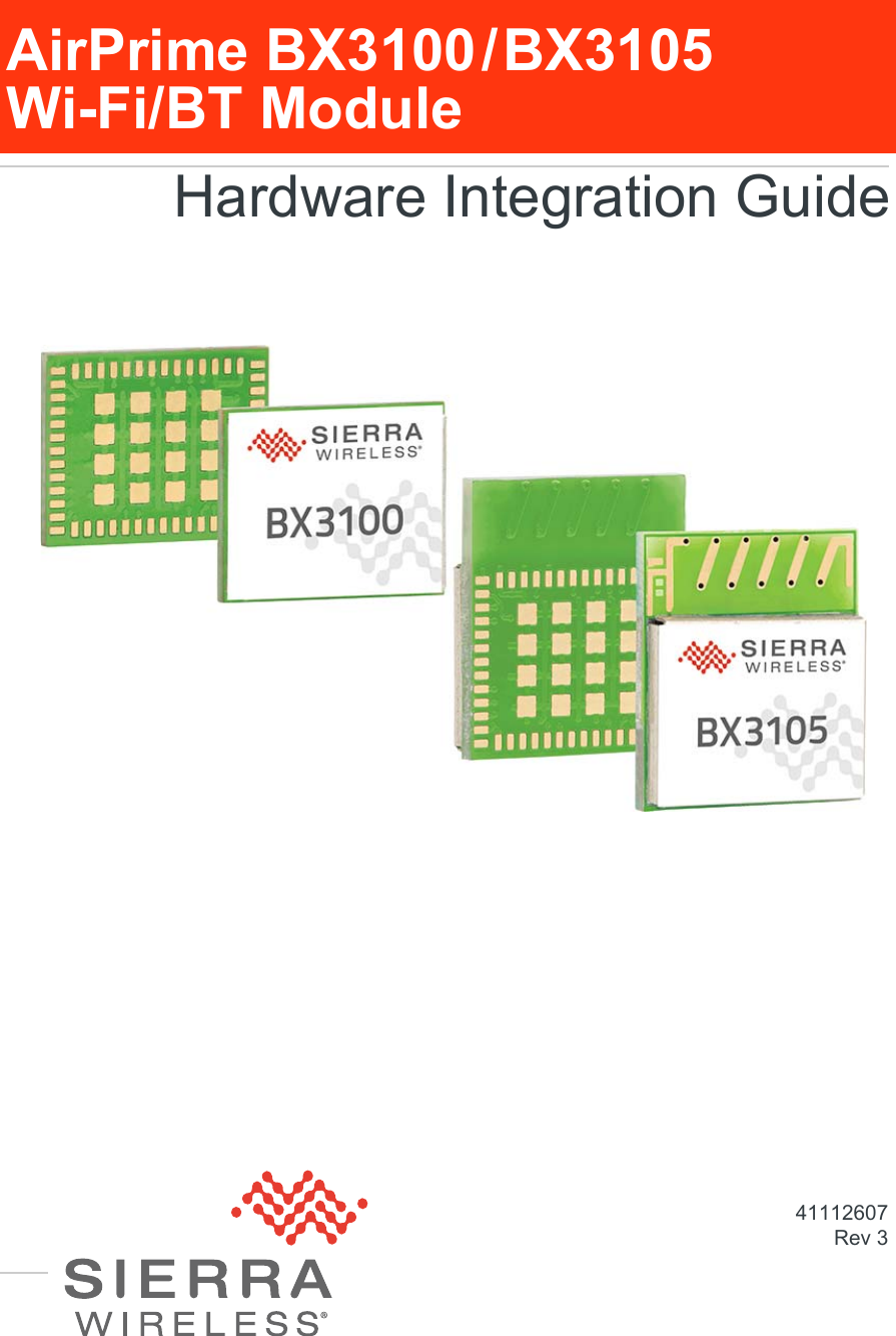
Sierra Wireless BX31A Radio Module User Manual AirPrime BX3100 BX3105 Wi Fi BT Module Hardware Integration Guide

Sierra Wireless Inc. Radio Module AirPrime BX3100 BX3105 Wi Fi BT Module Hardware Integration Guide

41112627 AirPrime BX3100-BX3105 Hardware Integration Guide r3
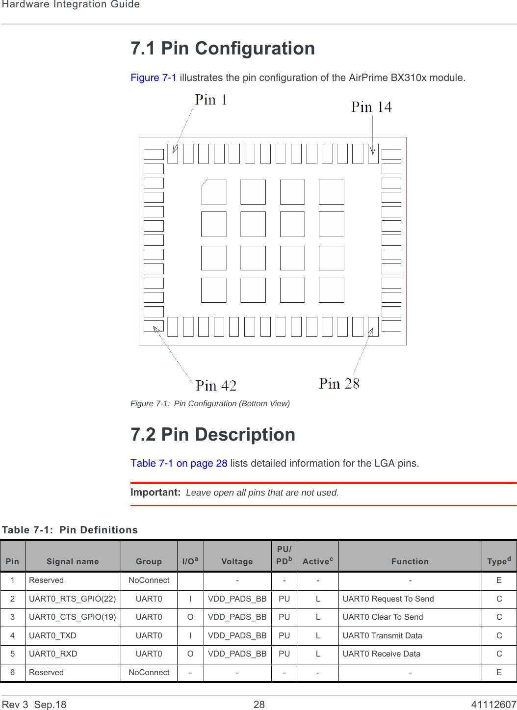
AirPrime BX3100/BX3105Wi-Fi/BT ModuleHardware Integration Guide41112607Rev 3
Hardware Integration GuideRev 3  Sep.18 2 41112607Important NoticeDue to the nature of wireless communications, transmission and reception of data can never be guaranteed. Data may be delayed, corrupted (i.e., have errors) or be totally lost. Although significant delays or losses of data are rare when wireless devices such as the Sierra Wireless modem are used in a normal manner with a well-constructed network, the Sierra Wireless modem should not be used in situations where failure to transmit or receive data could result in damage of any kind to the user or any other party, including but not limited to personal injury, death, or loss of property. Sierra Wireless accepts no responsibility for damages of any kind resulting from delays or errors in data transmitted or received using the Sierra Wireless modem, or for failure of the Sierra Wireless modem to transmit or receive such data.Safety and HazardsDo not operate the Sierra Wireless modem in areas where blasting is in progress, where explosive atmospheres may be present, near medical equipment, near life support equipment, or any equipment which may be susceptible to any form of radio interference. In such areas, the Sierra Wireless modem MUST BE IN AIRPLANE MODE OR POWERED OFF. The Sierra Wireless modem can transmit signals that could interfere with this equipment.Do not operate the Sierra Wireless modem in any aircraft, whether the aircraft is on the ground or in flight. In aircraft, the Sierra Wireless modem MUST BE IN AIRPLANE MODE OR POWERED OFF. When operating, the Sierra Wireless modem can transmit signals that could interfere with various onboard systems.Note: Some airlines may permit the use of cellular phones while the aircraft is on the ground and the door is open. Sierra Wireless modems may be used at this time.The driver or operator of any vehicle should not operate the Sierra Wireless modem while in control of a vehicle. Doing so will detract from the driver or operator's control and operation of that vehicle. In some states and provinces, operating such communications devices while in control of a vehicle is an offence.Limitation of LiabilityThe information in this manual is subject to change without notice and does not represent a commitment on the part of Sierra Wireless. SIERRA WIRELESS AND ITS AFFILIATES SPECIFICALLY DISCLAIM LIABILITY FOR ANY AND ALL DIRECT, INDIRECT, SPECIAL, GENERAL, INCIDENTAL, CONSEQUENTIAL, PUNITIVE OR EXEMPLARY DAMAGES INCLUDING, BUT NOT LIMITED TO, LOSS OF PROFITS OR REVENUE OR ANTICIPATED PROFITS OR REVENUE ARISING OUT OF THE USE OR INABILITY TO USE ANY SIERRA WIRELESS PRODUCT, EVEN IF SIERRA WIRELESS AND/OR ITS AFFILIATES HAS BEEN ADVISED OF THE POSSIBILITY OF SUCH DAMAGES OR THEY ARE FORESEEABLE OR FOR CLAIMS BY ANY THIRD PARTY.Notwithstanding the foregoing, in no event shall Sierra Wireless and/or its affiliates aggregate liability arising under or in connection with the Sierra Wireless product, regardless of the number of events, occurrences, or claims giving rise to liability, be in excess of the price paid by the purchaser for the Sierra Wireless product.
PrefaceRev 3  Sep.18 3 41112607Patents This product may contain technology developed by or for Sierra Wireless Inc. This product is manufactured or sold by Sierra Wireless Inc. or its affiliates under one or more patents licensed from MMP Portfolio Licensing.Copyright ©2018 Sierra Wireless. All rights reserved.Trademarks Sierra Wireless®, AirPrime®, AirLink®, AirVantage® and the Sierra Wireless logo are registered trademarks of Sierra Wireless, Inc.Windows® and Windows Vista® are registered trademarks of Microsoft Corporation.The Bluetooth® word mark and logos are registered trademarks owned by the Bluetooth SIG, Inc. and any use of such marks by Sierra Wireless is under license.Other trademarks are the property of their respective owners.Contact InformationRevision HistorySales information and technical support, including warranty and returnsWeb: sierrawireless.com/company/contact-us/Global toll-free number: 1-877-687-77956:00 am to 5:00 pm PSTCorporate and product information Web: sierrawireless.comRevision numberRelease date Changes1July 2018 Document created2July 2018 Updated Integrated PIFA gain3September 2018 Updated Regulatory textUpdated Wi-Fi Radio Generic Radio Characteristics table valuesUpdated Bluetooth Radio Generic Radio Characteristics table values
Rev 3  Sep.18 4 41112607Contents1: Introduction . . . . . . . . . . . . . . . . . . . . . . . . . . . . . . . . . . . . . . . . . . . . . . . . . . . . . . . . . . .61.1 Module Variants . . . . . . . . . . . . . . . . . . . . . . . . . . . . . . . . . . . . . . . . . . . . . . . . . . . . .61.2 General RF/Software Features  . . . . . . . . . . . . . . . . . . . . . . . . . . . . . . . . . . . . . . . . .61.2.1 Wi-Fi  . . . . . . . . . . . . . . . . . . . . . . . . . . . . . . . . . . . . . . . . . . . . . . . . . . . . . . . . .61.2.2 Bluetooth . . . . . . . . . . . . . . . . . . . . . . . . . . . . . . . . . . . . . . . . . . . . . . . . . . . . . .61.2.3 Interfaces   . . . . . . . . . . . . . . . . . . . . . . . . . . . . . . . . . . . . . . . . . . . . . . . . . . . . .71.2.4 Configuration Utility . . . . . . . . . . . . . . . . . . . . . . . . . . . . . . . . . . . . . . . . . . . . . .71.3 General Hardware Features   . . . . . . . . . . . . . . . . . . . . . . . . . . . . . . . . . . . . . . . . . . .71.3.1 Physical Dimensions and Connection Interface  . . . . . . . . . . . . . . . . . . . . . . . .72: Functional Specifications   . . . . . . . . . . . . . . . . . . . . . . . . . . . . . . . . . . . . . . . . . . . . . . .92.1 Features   . . . . . . . . . . . . . . . . . . . . . . . . . . . . . . . . . . . . . . . . . . . . . . . . . . . . . . . . . .93: Technical Specifications  . . . . . . . . . . . . . . . . . . . . . . . . . . . . . . . . . . . . . . . . . . . . . . .113.1 Environmental  . . . . . . . . . . . . . . . . . . . . . . . . . . . . . . . . . . . . . . . . . . . . . . . . . . . . .113.2 Power Supply Ratings  . . . . . . . . . . . . . . . . . . . . . . . . . . . . . . . . . . . . . . . . . . . . . . .113.3 Power Management   . . . . . . . . . . . . . . . . . . . . . . . . . . . . . . . . . . . . . . . . . . . . . . . .113.4 RF  . . . . . . . . . . . . . . . . . . . . . . . . . . . . . . . . . . . . . . . . . . . . . . . . . . . . . . . . . . . . . .123.4.1 Generic Radio  . . . . . . . . . . . . . . . . . . . . . . . . . . . . . . . . . . . . . . . . . . . . . . . . .123.4.2 Wi-Fi Radio  . . . . . . . . . . . . . . . . . . . . . . . . . . . . . . . . . . . . . . . . . . . . . . . . . . .123.4.3 Bluetooth Radio . . . . . . . . . . . . . . . . . . . . . . . . . . . . . . . . . . . . . . . . . . . . . . . .133.5 Electrical Specifications . . . . . . . . . . . . . . . . . . . . . . . . . . . . . . . . . . . . . . . . . . . . . .143.5.1 Absolute Maximum Ratings   . . . . . . . . . . . . . . . . . . . . . . . . . . . . . . . . . . . . . .144: Interfaces Specification  . . . . . . . . . . . . . . . . . . . . . . . . . . . . . . . . . . . . . . . . . . . . . . . .154.1 Overview  . . . . . . . . . . . . . . . . . . . . . . . . . . . . . . . . . . . . . . . . . . . . . . . . . . . . . . . . .154.2 UART . . . . . . . . . . . . . . . . . . . . . . . . . . . . . . . . . . . . . . . . . . . . . . . . . . . . . . . . . . . .154.3 ADC/Voltage Measurement   . . . . . . . . . . . . . . . . . . . . . . . . . . . . . . . . . . . . . . . . . .164.4 I2C Interface  . . . . . . . . . . . . . . . . . . . . . . . . . . . . . . . . . . . . . . . . . . . . . . . . . . . . . .174.4.1 Application . . . . . . . . . . . . . . . . . . . . . . . . . . . . . . . . . . . . . . . . . . . . . . . . . . . .174.5 I2S Interface (Digital Audio) . . . . . . . . . . . . . . . . . . . . . . . . . . . . . . . . . . . . . . . . . . .184.6 General Purpose Input/Output (GPIO)  . . . . . . . . . . . . . . . . . . . . . . . . . . . . . . . . . .18
ContentsRev 3  Sep.18 5 411126074.7 Bootstrap Pins . . . . . . . . . . . . . . . . . . . . . . . . . . . . . . . . . . . . . . . . . . . . . . . . . . . . . 194.8 SPI Bus  . . . . . . . . . . . . . . . . . . . . . . . . . . . . . . . . . . . . . . . . . . . . . . . . . . . . . . . . . .204.9 Secure Digital IO (SDIO) Interface  . . . . . . . . . . . . . . . . . . . . . . . . . . . . . . . . . . . . . 214.10 Module Enable  . . . . . . . . . . . . . . . . . . . . . . . . . . . . . . . . . . . . . . . . . . . . . . . . . . . 224.11 PWM  . . . . . . . . . . . . . . . . . . . . . . . . . . . . . . . . . . . . . . . . . . . . . . . . . . . . . . . . . . . 225: General Layout Recommendations  . . . . . . . . . . . . . . . . . . . . . . . . . . . . . . . . . . . . . . 236: Regulatory Compliance  . . . . . . . . . . . . . . . . . . . . . . . . . . . . . . . . . . . . . . . . . . . . . . . . 246.1 United States   . . . . . . . . . . . . . . . . . . . . . . . . . . . . . . . . . . . . . . . . . . . . . . . . . . . . . 246.2 Canada  . . . . . . . . . . . . . . . . . . . . . . . . . . . . . . . . . . . . . . . . . . . . . . . . . . . . . . . . . . 257: Pinout  . . . . . . . . . . . . . . . . . . . . . . . . . . . . . . . . . . . . . . . . . . . . . . . . . . . . . . . . . . . . . . 277.1 Pin Configuration   . . . . . . . . . . . . . . . . . . . . . . . . . . . . . . . . . . . . . . . . . . . . . . . . . . 287.2 Pin Description  . . . . . . . . . . . . . . . . . . . . . . . . . . . . . . . . . . . . . . . . . . . . . . . . . . . . 288: References  . . . . . . . . . . . . . . . . . . . . . . . . . . . . . . . . . . . . . . . . . . . . . . . . . . . . . . . . . . 328.1 Web Site Support  . . . . . . . . . . . . . . . . . . . . . . . . . . . . . . . . . . . . . . . . . . . . . . . . . . 328.2 Reference Documents   . . . . . . . . . . . . . . . . . . . . . . . . . . . . . . . . . . . . . . . . . . . . . . 329: Abbreviations    . . . . . . . . . . . . . . . . . . . . . . . . . . . . . . . . . . . . . . . . . . . . . . . . . . . . . . . 33
Rev 3  Sep.18 6 4111260711: IntroductionThis document defines and illustrates the AirPrime BX310x (BX3100, BX3105) Wi-Fi/BT Host-less module’s high-level product features, interfaces, and hardware features (including electrical and mechanical performance criteria).1.1 Module VariantsAirPrime BX310x module variants include:•AirPrime BX3100—External antenna connection•AirPrime BX3105—Embedded antenna1.2 General RF/Software FeaturesThe AirPrime BX310x is a low-power, small form-factor self-contained Wi-Fi/Bluetooth® (Wi-Fi/BT) module.With an embedded software suite, the BX310x is an ideal solution for developers who want to quickly and cost-effectively integrate Wi-Fi/BT functionality into their products.The following table summarizes the module’s supported wireless frequencies and modes:1.2.1 Wi-FiThe AirPrime BX310x supports 2.4 GHz Wi-Fi operation. Key features include:•TCP/IP•802.11 b/g/n/e/i•Connection methods—BSS STA, SoftAP•Transmit power—Adjustable, up to 20 dBm (maximum)For a list of additional supported Wi-Fi functionality, protocols, and features, see Features on page 9.1.2.2 BluetoothThe AirPrime BX310x supports 2.4 GHz Bluetooth classic and BLE operation. Key features include:•Bluetooth v4.2 BR/EDR and BLE compliant•SPP (Serial Port Profile)For a list of additional supported Bluetooth functionality, protocols, and features, see Features on page 9.Table 1-1: Supported RF FrequenciesTechnology RF band NotesWi-Fi2.4GHz (2.400–2.485 GHz)•802.11b/g/n/e/i•Max data rate—MCS7 HT40 150 MbpsBluetooth •v4.2 BR/EDR and BLE compliant
IntroductionRev 3  Sep.18 7 411126071.2.3 InterfacesThe AirPrime BX310x provides the following interfaces and peripheral connectivity:•Power supply—See Power Supply Ratings on page 11.•RF—See RF on page 12.•UART serial link—See UART on page 15.•ADC/Voltage measurement—See ADC/Voltage Measurement on page 16.•I2C—See I2C Interface on page 17.•Digital audio (I2S)—See I2S Interface (Digital Audio) on page 18.•GPIOs—See General Purpose Input/Output (GPIO) on page 18.•SPI bus—See SPI Bus on page 20.•SDIO—See Secure Digital IO (SDIO) Interface on page 21.•Module enable—See Module Enable on page 22.•PWM—See PWM on page 22.1.2.4 Configuration UtilityThe AirPrime BX310x includes a browser-based utility for device configuration. For usage details, refer to [1] AirPrime BX310x AT Command Reference available at source.sierrawireless.com.1.3 General Hardware Features1.3.1 Physical Dimensions and Connection InterfaceAirPrime BX310x modules are compact, robust, fully shielded and laser-marked modules with the dimensions noted in Table 1-2.The AirPrime BX310x module is an LGA form factor device. All electrical and mechanical connections are made through the 70 Land Grid Array (LGA) pads on the bottom side of the PCB. (See Figure 7-1 on page 28 for details.)Table 1-2: AirPrime BX310x Dimensionsaa. Dimensions are accurate as of the release date of this document.ParameterNominalTolerance UnitsBX3100bb. BX3100 is a CF3 xSmall module, which belongs to the Common Flexible Form Factor (CF3) family of WWAN modulesBX3105Length 11.5 13.5 ±0.10 mmWidth 9.5 11.5 ±0.10 mmThickness 2.4 2.4 ±0.20 mmWeight 0.56 0.65 ±0.10 g
Hardware Integration GuideRev 3  Sep.18 8 41112607The LGA pads have the following distribution:Table 1-3: LGA Pad TypesPad Type / Quantity Dimensions PitchSignal Pads 54 outer pads 0.75x0.35 mm 0.65 mmGround Pads 16 inner pads 1.0x1.0 mm 1.83 mm/1.48 mm
Rev 3  Sep.18 9 4111260722: Functional Specifications2.1 FeaturesTable 2-1 summarizes the AirPrime BX310x module’s RF (Wi-Fi and Bluetooth), Power, software, and hardware capabilities.Note: Table contents are preliminary and subject to change.Table 2-1: AirPrime BX310x CapabilitiesFeature DescriptionModule•Secure boot•Secure update•FOTA (Firmware update Over The Air)•Sierra Wireless AirVantage support•CF3-compliant footprint (BX3100)Wi-Fi•Protocols:·802.11 b/g/n/e/i·802.11 n (2.4 GHz), up to 150 Mbps; MCS0-7 in 20/40 MHz bandwidths·Receiving STBC (Space-time Block Code) 2x1·802.11 e: QoS for wireless multimedia technology·Additional 802.11i security features (pre-authentication, TSN, etc.)·WMM-PS, UAPSD·A-MPDU, A-MSDU aggregation·Block ACK  (RTS/CTS/ACK/BA)·Fragmentation/defragmentation·CCMP (CBC-MAC, counter model), TKIP (MIC, RC4), WAPI (SMS4), WEP (RC4), CRC·Frame encapsulation (802.11h/RFC 1042)·Pre-authentication, TSN•Supported channels—1–14•Data transfer (HTTP, HTTPS, MQTT, TCP/UDP)•Autoconnection—After device reset, automatically connects to available AP based on previous configuration•Infrastructure BSS Station mode/SoftAP mode: AP mode, STA mode, concurrent AP/STA mode •Up to 8asimultaneous Wi-Fi clients•IP configuration—IP address in STA mode via DHCP or static assignment•Authentication (security) modes: WPA, WPA2, WPA/WPA2, WPA2 Enterprise•UMA-compliant and certified•Open interface for various upper layer authentication schemes over EAP (e.g. TLS, PEAP, LEAP, SIM, AKA, customer-specific)•Adaptive rate fallback algorithm•Automatic retransmission/response on slow hosts
Hardware Integration GuideRev 3  Sep.18 10 41112607Bluetooth•Bluetooth v4.2 BR/EDRb and BLE compliant•Supported channels: BT Classicb—0–78; BLE—0–39•Supported v4.2 modes: BRb (Basic Rate); EDRb (Enhanced Data Rate); LE (Low Energy)•BTb classic mandatory features•BT low-energy mandatory features•Class 1/Class 2/Class 3 transmitter without external power amplifier•Class 1 operation without external PA•Enhanced power control (>30 dB dynamic control range)•+10 dBm transmitting power•NZIF receiver with -98 dBm sensitivity•Modulation—p/4 DQPSKb, 8 DPSKb•ACLb, SCOb, eSCOb•Adaptive Frequency Hopping (AFH)•BT 4.2 controller and host stackb•Service Discover Protocol (SDP)b•General Access Profile (GAP)•Security Manage Protocol (SMP)b•Bluetooth Low Energy (BLE)•ATT/GATT•BLE Beaconb•SPPb, RFCOMM•Profiles: Wi-Fi Autoconnection—After device reset, automatically connects to available AP based on previous configuration.•UART features: GATT profiles, Define personal services•Roles—Simultaneous Central (access point)/Peripheral (client)•Simultaneous connections:·Up to 7a(total) simultaneous connections, including up to 3aBLE connec-tions·Simultaneous BT Classicb and BLE connections•PCMb/I2SbConfigurationDevice configuration methods:•Built-in web-based configuration utility. See Configuration Utility on page 7.•AT commands available over UART, Wi-Fi, and BT links. Refer to [1] AirPrime BX310x AT Command Reference at source.sierrawireless.com.Security•All standard IEEE802.11 security features, including WFA, WPA/WPA2, WAPI•Secure boot•Flash encryption•Cryptographic hardware acceleration: AES, HASH (SHA-2) library, RSA, ECC, Random Number Generator (RNG)Power managementMultiple power modesb to reduce power consumption: Active, Radio off, Light sleep, Deep sleep, HibernationSleep Patterns: Association sleep pattern, ULP sensor-monitored patternba. Subject to firmware support and RAM limitations.b. Support pending firmware upgrade.Table 2-1: AirPrime BX310x Capabilities (Continued)Feature Description
Rev 3  Sep.18 11 4111260733: Technical Specifications3.1 EnvironmentalThe environmental specifications for operation and storage of the AirPrime BX310x are defined in Table 3-1.3.2 Power Supply RatingsDC power is supplied via the pins described in Table 3-2 on page 11.Note: Operation above the maximum specified operating voltage (see Table 3-8 on page 14) is not recommended, and specified typical performance or functional operation of the device is neither implied nor guaranteed.3.3 Power ManagementThe AirPrime BX310x switches between several power modes to minimize current consumption.Light Sleep and Deep Sleep modes are enabled via AT commands from the host. Refer to [1] AirPrime BX310x AT Command Reference for details.Table 3-1: Environmental SpecificationsParameter RangeAmbient Operating Temperature -40°C to +85°CAmbient Storage Temperature -40°C to +105°C(Recommended)Table 3-2: Power Supply PinsPin Name Voltage Direction Function33 VGPIO 3.3V Output Supply voltage reference for secondary I2C interface (pins 53/54)50 VDD_3V3_RF 2.3–3.6V Input RF/Analog signal power supply51 VDD_3V3_PA 2.3–3.6V Input Internal Power Amplifier power supply52 VDD_PADS_BB 2.7–3.6V Input Baseband/Digital I/O power supply
Hardware Integration GuideRev 3  Sep.18 12 41112607Table 3-3 describes the AirPrime BX310x’s supported power modes.3.4 RF3.4.1 Generic RadioMeasurements conducted at 25C ambient temperature.3.4.2 Wi-Fi RadioMeasurements conducted at 25C ambient temperature.Table 3-3: Power Modes — DescriptionsPower Mode CPUWi-Fi/BT radio /baseband RTCULP co-processor NotesActive On On On On Fully functionalRadio offaOn Off On OnLight sleepaPause Off On On Wake up events will wake the module.Deep sleepaOff Off On On/Off Connection data stored in RTC memoryHibernateaOff Off Off Off Only RTC timer or specific RTC GPIOs can wake the module.a. Available in future firmware release.Table 3-4: Generic Radio CharacteristicsDescription Min Typ Max UnitBX3100 RF Port Impedance 50 Frequency Band 2.4 2.45 2.485 GHzBX3105 Antenna Gain 0dBiTable 3-5: Generic Radio CharacteristicsDescription Min Typ Max UnitTransmit 802.11b, CCK 1 Mbps, Conducted Tx Power, EVM and Mask Compliant 14 15.5 17 dBmTransmit 802.11g, OFDM 6 Mbps, Conducted Tx Power, EVM and Mask Compliant 14a15.5a17adBmTransmit 802.11n, MCS0 HT20 6.5 Mbps, Conducted Tx Power, EVM and Mask Compliant 14b15.5b17bdBmTransmit 802.11n, MCS0 HT40 13.5 Mbps, Conducted Tx Power, EVM and Mask Compliant 14c15.5c17cdBmConducted Receiver Sensitivity 11b DSSS, 1 Mbps -98 -95 -93 dBmConducted Receiver Sensitivity 11b CCK, 11 Mbps -90 -87 -84 dBmConducted Receiver Sensitivity 11g OFDM, 6 Mbps -94 -91 -88 dBm
Technical SpecificationsRev 3  Sep.18 13 411126073.4.3 Bluetooth RadioMeasurements conducted at 25C ambient temperature.Conducted Receiver Sensitivity 11g OFDM, 54 Mbps -73 -71.5 -70 dBmConducted Receiver Sensitivity 11n HT20 OFDM, 72.2 Mbps -73 -71 -69 dBmConducted Receiver Sensitivity 11n HT40 OFDM, 135 Mbps -73 -71 -69 dBmConducted Harmonics 2F0 --42 -39 dBmConducted Harmonics 3F0 --54 -51 dBma. Channel 1&11 power is automatically reduced for FCC 15.205 band edge compliance, reduction is 2 dB.b. Channel 1&11 power is automatically reduced for FCC 15.205 band edge compliance, reduction is 2.5 dB.c. Channel 1&11 typical power is automatically reduced for FCC 15.205 band edge compliance, reduction is 3 dB.Table 3-5: Generic Radio Characteristics (Continued)Description Min Typ Max UnitTable 3-6: Generic Radio CharacteristicsDescription Min Typ Max UnitTransmit Power BR 1 Mbps 7.5 910.5aa. Maximum Output power is restricted by compliance to FCC 15.205 band edge to 5.5 dBm Max.dBmTransmit Power EDR 2 Mbps 7.5 910.5 dBmTransmit Power EDR 3 Mbps 7.5 910.5 dBmTransmit Power LE 1 Mbps 2.5 45.5 dBmReceiver Sensitivity BR 1 Mbps -89 -88 -87 dBmReceiver Sensitivity EDR 2 Mbps -87 -86 -85 dBmReceiver Sensitivity EDR 3 Mbps -81 -82.5 -84 dBmReceiver Sensitivity LE 1 Mbps -92.5 -91 -89 dBmOut-of-band blocking performance 30 MHz~2000 MHz --10 -dBmOut-of-band blocking performance 2000 MHz~2400 MHz --27 -dBmOut-of-band blocking performance 2500 MHz~3000 MHz --27 -dBmOut-of-band blocking performance 3000 MHz~12.5 GHz --10 -dBm
Hardware Integration GuideRev 3  Sep.18 14 411126073.5 Electrical Specifications3.5.1 Absolute Maximum Ratings Table 3-7: Absolute Maximum RatingsParameter Min Max UnitsVIL Input low voltage -0.3 0.25VIO VVIH Input high voltage 0.75VIO 3.6 VIIL Input leakage current -50 nAVOL Output low voltage -0.1VIO VVOH Output high voltage 0.8VIO - VCpad Input pin capacitance - 2 pFVIO VDD_PADS_BB 2.7 3.6 VIMAX GPIO maximum drive capability -12 mATSTR Storage temperature range -40 150 CTable 3-8: Recommended Operating ConditionsParameter Min Typ Max UnitsVDD Supply voltage (VDD_3V3_PA, VDD_3V3_RF) 2.3 3.3 3.6 VVIO I/O supply voltage (VDD_PADS_BB) 2.7 3.3 3.6 VTOPR Operating temperature range -40 -85 CVIL CMOS low level input voltage 0 - 0.3VIO VVIH CMOS high level input voltage 0.7VIO - VIO VVTH CMOS threshold voltage -0.5VIO - V
Rev 3  Sep.18 15 4111260744: Interfaces Specification4.1 OverviewThis section describes the interfaces supported by the AirPrime BX310x embedded module and provides specific voltage, timing, and circuit recommendations for each interface.4.2 UARTThe AirPrime BX310x provides one UART interface for asynchronous communication between the AirPrime BX310x module and a host device (e.g. a PC or host processor):•UART0—4-wire, RS-232-compliant interfaceNote: Up to two additional UART interfaces can be added by configuring GPIOs using AT commands.Flow control is managed using:•RTS/CTS signals (This method is required for higher UART interface speeds.)or•Software XON/XOFFTable 4-1 on page 15 describes the signals used for UART0.Note: UART signals are named with respect to the HOST, and directions are listed with respect to the module. For example, UART0_RXD is an output from the module to the host.The UART interface is configurable via AT commands:•Default configuration—115200 (baudrate), 8 bit, no parity, no handshaking•Baudrate considerations:·Maximum supported—5 Mbaud·Maximum tested—3 Mbaud. This is the maximum baudrate supported by the BX310x Dev Kit FTDI converter IC.·HW handshaking is recommended above rates of 1 Mbaud and can be enabled via AT command (AT&K3).Table 4-1: UART0 PinsaPin Interface Name Direction Function Voltage Level2UART0UART0_RTS IReady To Send, flow controlVDD_PADS_BB3UART0_CTS OClear To Send, flow control4UART0_TXD ITransmit Data5UART0_RXD OReceive Dataa. If UART0 pins are not used, leave open.
Hardware Integration GuideRev 3  Sep.18 16 41112607·Common baud rates are supported—any baud rate in the supported range can be selected via AT+IPR=<uart_baud_rate> command. The device automatically configures the clock dividers appropriately for the chosen baud rate.·Baud rates are persistent post-reset.·Recommendation—Add series termination resistors close to the module in the UART lines for management of clock harmonics. 499 resistors are recommended.4.3 ADC/Voltage MeasurementThe AirPrime BX310x provides a general purpose ADC (Analog to Digital Converter) input, which can sample multiple inputs configured using AT commands.Pins VDET_1, VDET_2, SENSOR_VP, and SENSOR_VN are used to measure single-ended analog voltages referenced to ground. The voltage on these pins is read via an AT command.Noise can have a large impact on sensitive voltage measurements. To improve the accuracy of small voltage level measurements, a100 nF capacitor to ground is recommended on the input to the VDET_1, VDET_2, SENSOR_VP, and SENSOR_VN pins.  Access to a Hall effect sensor is supported via firmware, and is selected using AT commands.The sensor pins (SENSOR_VP or SENSOR_VN) will trigger an input perturbation (glitch) lasting for 80 ns when the ADC or Hall sensor is initialized.Table 4-2: ADC Interface Pinsaa. Leave open any pins that are not used.Pin Signal name Directionbb. Signal direction with respect to the module.Function Voltage Level18 VDET_1 IAnalog to Digital Converter VDD_PADS_BB19 VDET_2 ITable 4-3: Voltage-measurement GPIO Pinsaa. Leave open any pins that are not used.Pin Signal Name Directionbb. Signal direction with respect to the module.Voltage level31 SENSOR_VP IVDD_PADS_BB32 SENSOR_CAPP I34 SENSOR_CAPN I36 SENSOR_VN I
Interfaces SpecificationRev 3  Sep.18 17 411126074.4 I2C InterfaceThe AirPrime BX310x module provides two I2C (Inter-Integrated Circuit) dedicated serial ports (bus interface) based on [2] The I2C Bus Specification, Version 2.1, January 2000 (Phillips Semiconductor document number 9398 393 40011).The interfaces use the pins indicated in Table 4-4.This implementation of the I2C interface includes the following characteristics:•Supported voltage:·Primary I2C (3.3 V, configurable)·Secondary I2C (3.3 V)•Standard-mode interface—Data transfer rates up to 100 kbit/s•Fast-mode interface—Data transfer rates up to 400 kbit/s)•Master mode operation•Addressing modes—7-bit; 10-bit; Dual addressing modeExternal 2.2 k pull-up resistors must be applied to I2C signals (see Figure 4-1 on page 17).For I2C bus details, including I2C bus waveform and timing details, refer to the I2C Bus Specification.4.4.1 ApplicationFigure 4-1: Example of I2C Bus ApplicationTable 4-4: I2C Interface Pinsaa. Leave open any pins that are not used.Pin Signal name Direction Function Voltage Level9I2C1_SCL I/O Primary I2C interfaceVDD_PADS_BB17 I2C1_SDA I/O Primary I2C interface53 I2C2_SDA I/O Secondary I2C interfaceVGPIO54 I2C2_SCL I/O Secondary I2C interfaceAirPrime BX310xWi-Fi/BT ModuleCustomerApplicationI2C1_SDAI2C1_SCL 2.2K 2.2KVDD_PADS_BBI2C2_SCLI2C2_SDA 2.2KVGPIO2.2K
Hardware Integration GuideRev 3  Sep.18 18 411126074.5 I2S Interface (Digital Audio)Note: Interface support is forthcoming.The AirPrime BX310x provides a 4-wire I2S (digital audio) interface that can be used to transfer serial digital audio to or from an external stereo DAC/ADC, and supports the following features:•Modes—Master, Slave•Transmission format—Full duplex, Half duplex•Resolution (bits per frame)—8, 16, 32, 40, 48•Channels—Input, Output•Bit clock—10 kHz–40 MHz•Supported audio interfaces (forthcoming)—PDM (Pulse Density Modulation), BT PCM (Pulse Code Modulation)The interface uses the pins indicated in Table 4-5.4.6 General Purpose Input/Output (GPIO)The AirPrime BX310x defines several GPIOs for customer use, as described in Table 4-6 and Table 4-7.Note: The pins carrying the ‘Alternate function’ GPIOs are multi-function. The alternate inter-faces (SDIO or SPI) can be selected via an AT command.   Table 4-5: I2S Interface Pinsaa. Leave open any pins that are not used.Pin Signal name Directionbb. Signal direction with respect to the module.Function Voltage Level16 I2S_MCLK OI2S MasterClockVDD_PADS_BB24 I2S_DO OI2S Data Out25 I2S_DI II2S Data In26 I2S_LRCLK I/O I2S Left-Right Clock (Word Select)27 I2S_BCLK I/O I2S Bit ClockTable 4-6: GPIO Pins (Dedicated)aa. Leave open any pins that are not used.Pin Signal Name Direction Default State Function Voltage Level14 GPIO(5) I/O Pull highbb. Pulled high internallyGeneral purpose I/O VDD_PADS_BB35 GPIO(27) I/O No pullcc. Internal configuration— no internal pull-ups
Interfaces SpecificationRev 3  Sep.18 19 411126074.7 Bootstrap PinsThe GPIOs listed in Table 4-8 are used as Bootstrap pins during start-up.Table 4-7: GPIO Pins (Alternate function)aPin Signal Name Direction Default State Function Voltage Level9GPIO(23)I/ONo pullbGeneral purpose I/O VDD_PADS_BB16 GPIO(0) Pull highc17 GPIO(25) No pullb18 GPIO(34) No pullb19 GPIO(35) No pullb24 GPIO(32) No pullb25 GPIO(33) No pullb26 GPIO(18) No pullb27 GPIO(26) No pullb31 GPIO(36) No pullb32 GPIO(37) No pullb34 GPIO(38) No pullb36 GPIO(39) No pullb42 GPIO(15) Pull highc d43 GPIO(12) Pull lowe44 GPIO(14) Pull highc45 GPIO(13) Pull highc46 GPIO(2) Pull lowe47 GPIO(4) Pull lowe53 GPIO(16) No pullb54 GPIO(17) No pullba. Leave open any pins that are not used.b. Internal configuration—no internal pull-upsc. Pulled high internallyd. GPIO(15) default state (pull HIGH) enables UART boot messaging. To disable UART boot mes-sages, drive GPIO(15) LOW prior to boot.e. Pulled low internally
Hardware Integration GuideRev 3  Sep.18 20 41112607   4.8 SPI BusNote: Interface support is forthcoming.The AirPrime BX310x provides one 6-wire Serial Flash SPI-compatible interface (SPI Master).Note: Traditional 5-wire (MOSI/MISO/SCLK/CS/SRDY) SPI Slave interface can also be implemented over this same interface.Table 4-10 describes the SPI interface pins for both configurations (5- and 6-wire).Note: The pins carrying the SPI interface are multi-function. The alternate interfaces (SDIO or GPIO) can be selected via an AT command.Table 4-8: GPIO Bootstrap FunctionsGPIO Function Default State Default Function Alternative0Boot Source High, Internal pull 45 kBoot from Internal Flash Download to Flash (Disabled)2Boot Source High, Internal pull 45 k5SDIO Slave TimingHigh, Internal pull 45 kRising Edge Input & Output See Table 4-9.15 (MTDO) High, Internal pull 45 k12 (MTDI) SDIO Interface Voltage Low, Internal pull 45 k3.3V 1.8V (Not supported)Table 4-9: SDIO Slave Timing ConfigurationGPIO(5) GPIO(15) ConfigurationLow Low Falling Edge Input & OutputLow High Rising Edge Input, Falling Edge OutputHigh Low Falling Edge Input, Rising Edge OutputHigh High Rising Edge Input & OutputTable 4-10: SPI Pin DescriptionsaPinSPI Master SPI Slave DirectionbFunction6-Wire Signal Name 5-Wire Signal Name Master Slave42 HSPICS0 CS O I SPI Chip Select43 HSPIQ MISO I O MISO44 HSPICLK SCLK O I SPI Clock
Interfaces SpecificationRev 3  Sep.18 21 411126074.9 Secure Digital IO (SDIO) InterfaceNote: Interface support is forthcoming.The AirPrime BX310x defines one SDIO slave-controller interface (SD 2.0-compliant), which supports connections to SD memory and I/O cards.The following features are supported:•SPI/1-bit/4-bit modes•Data transfer rates—0–50 MHz•Block size—Up to 512 bytes•Interrupts—Module-initiated and host-initiated•Module-initiated data transfer via host interrupt•Configurable features—Sampling, driving clock edge•Registers for direct access by hostTable 4-11 describes the signals used for SDIO.Note: The pins carrying the SDIO interface are multi-function. The alternate interfaces (GPIO or SPI) can be selected via an AT command.  45 HSPID MOSI O I MOSI46 HSPIWP - O - Write Protect (M)47 HSPIHD SRDY O O Holda. Leave open any pins that are not used.b. Signal direction with respect to the module.Table 4-11: SDIO Pin Descriptionsaa. Leave open any pins that are not used.Pin Signal Name Direction Function42 SD_CMD I/O SDIO command43 SD_DATA2 I/O SDIO data bit 244 SD_CLK OSDIO clock45 SD_DATA3 I/O SDIO data bit 346 SD_DATA0 I/O SDIO data bit 047 SD_DATA1 I/O SDIO data bit 1Table 4-10: SPI Pin Descriptionsa (Continued)PinSPI Master SPI Slave DirectionbFunction6-Wire Signal Name 5-Wire Signal Name Master Slave
Hardware Integration GuideRev 3  Sep.18 22 41112607SDIO is particularly susceptible to tracking impedance and length variations between the SDIO tracks. Ensure that controlled impedance tracking is used, and minimize tracking length between the module and SD slave device. Add series resistor footprints at the host end to decrease the drive current and reduce potential interference, and match the length of all the SD tracks to within 1 mm.SDIO tracking can cause significant radiated interference at integer multiples of the SD clock frequency, which can be picked up by the BX310x antenna. Bury SDIO tracks between ground planes and ensure stitching ground vias are placed throughout the board surrounding the SDIO tracking.SDIO timing during the boot process is provided by GPIO(5) and GPIO(15). See Table 4-9 on page 20 for details.4.10 Module EnableThe AirPrime BX310x uses the ENABLE (Module Enable) signal to turn the module on/off:•Turn module on—Drive ENABLE high (to VDD_PADS_BB)•Turn module off—Drive ENABLE low (to 0V)To avoid a possible implementation-dependent issue where enabling/disabling Wi-Fi functionality could cause a perturbation (glitch) on the power supply rails that impacts module operations, a short delay (1 ms recommended) is required for the power supply to stabilize before enabling the module.If ENABLE is controlled by the Host, the host implements the delay (from the time the supply is present) before driving ENABLE high.If ENABLE is hard-wired to the supply (VDD_PADS_BB), an RC circuit (10k & 0.1uF) is required. The RC circuit will create the required delay, allowing the supply to stabilize before ENABLE is pulled high.Do not leave this pin unconnected.4.11 PWMThe AirPrime BX310x supports the use of PWM functionality on GPIOs (GPIO(5) and GPIO(27)) via AT command configuration. Refer to [1] AirPrime BX310x AT Command Reference for details.Table 4-12: Enable Pin DescriptionPin Signal Name Directionaa. Signal direction with respect to the module.Function Voltage Level37bb. Do not leave this pin unconnected.ENABLE IStart/stop module VDD_PADS_BB
Rev 3  Sep.18 23 4111260755: General Layout RecommendationsIn addition to specific requirements for the antenna implementation and clearance of the BX3105 detailed in this document, good mixed-signal layout practices should be followed:•Avoid tracking of high frequency signals near the RF sections of the module.•Ensure plenty of ground vias throughout the application board.•Tightly tie ground planes together throughout the application board.•BX3100 RF tracking to application board antenna or RF connector:·Use 50  impedance controlled tracks.·Do not track near sources of digital interference.·Provide continuous unbroken ground plane reference.·Avoid multiple layer changes.•Supply decoupling should be placed as close to the supply pins as possible.•Avoid long digital tracks on surface layers—they may support significant RF harmonic content.
Rev 3  Sep.18 24 4111260766: Regulatory ComplianceCaution: Unauthorized modifications or changes not expressly approved by Sierra Wireless could void compliance with regulatory rules, and thereby your authority to use this equipment.The BX3100/BX3105 module is designed to meet the requirements of the following regulatory bodies and regulations, where applicable:•Federal Communications Commission (FCC) of the United States•Innovation, Science and Economic Development Canada (ISED)•Ministry of Internal Affairs and Communications (MIC) of Japan•Radio Equipment Directive of the European Union•Ministry of Industry and Information Technology (People’s Republic of China)•The National Communications Commission (NCC) of Taiwan, Republic of China•The National Telecommunications Agency (ANATEL)•National Radio Research Agency (South Korea)Note: To determine whether specific approvals have been received or to obtain the anticipated schedule for approvals, please contact your Sierra Wireless account representative.Upon commercial release, the following industry certification will have been obtained, where applicable:•Bluetooth SIGAdditional certifications and details on specific country approvals may be obtained upon customer request — contact your Sierra Wireless account representative for details.Additional testing and certification may be required for the end product with an embedded BX3100/BX3105 module and are the responsibility of the OEM. Sierra Wireless offers professional services-based assistance to OEMs with the testing and certification process, if required.6.1 United StatesThe BX3100/BX3105 module has been certified by the Federal Communications Commission under FCC ID: N7NBX31A. The BX3105 module is certified with an on-board antenna, while the BX3100 module is certified with an external antenna.Integrators may use the BX3100/BX3105 modules in their end products without additional FCC certification if they meet the following conditions. Otherwise, additional FCC approval must be obtained.1. Only antennas of the same type and with equal or less gains as shown in Table 6-1 may be used. Other types of antennas and/or higher gain antennas may require additional authorization for operation.2. The end product integrating the BX3100 module must use the RF trace design approved with the BX3100 module. Details of the trace design can be obtained from Sierra Wireless upon request.3. At least 6 cm separation distance between the antenna and the user’s body, or 2.5 cm separation distance when the end product is designed or intended for use FCC ID: N7NBX31A
Regulatory ComplianceRev 3  Sep.18 25 41112607on extremities, or mainly operated in extremity-only exposure conditions, i.e., hands, wrists, feet and ankles, must be maintained at all times.4. The regulatory label on the end product must include the text “Contains FCC ID: N7NBX31A” and the following compliance statement:This device complies with Part 15 of the FCC Rules. Operation is subject to the following two conditions: (1) This device may not cause harmful interference, and (2) this device must accept any interference received, including interference that may cause undesired operation.5. A user manual with the end product must clearly indicate the operating require-ments and conditions that must be observed to ensure compliance with current FCC RF exposure guidelines.6. End users must not be provided with access to configuration options to change technical parameters of the BX3100/BX3105 module, except as permitted by the FCC rules.The end product with an embedded BX3100/BX3105 module may also need to meet the requirements in FCC Part 15 Subpart B for unintentional radiators and be properly authorized.6.2 CanadaThis radio transmitter IC: 2417C-BX31A has been approved by Innovation, Science and Economic Development Canada to operate with the antenna types listed below, with the maximum permissable gain indicated. Antenna types not included in this list that have a gain greater than the maximum gain indicated for any type listed are strictly prohibited for use with this device.Integrators may use the BX3100/BX3105 modules in their end products without additional ISED certification if they meet the following conditions. Otherwise, additional ISED approval must be obtained.1. Only antennas of the same type and with equal or less gains as shown in Table 6-1 may be used. Other types of antennas and/or higher gain antennas may require additional authorization for operation.2. The end product integrating the BX3100 module must use the RF trace design approved with the BX3100 module. Details of the trace design can be obtained from Sierra Wireless upon request.3. At least 4.5 cm separation distance between the antenna and the user’s body, or 3 cm separation distance when the end product is designed or intended for use on extremities, or mainly operated in extremity-only exposure conditions, i.e., hands, wrists, feet and ankles, must be maintained at all times.Table 6-1: Antenna SpecificationsModule Antenna Type Maximum GainBX3105 Integrated PIFA -1.65 dBiBX3100Monopole 0dBiDipole 2.5 dBi @ 2.4 GHzIC: 2417C-BX31A
Hardware Integration GuideRev 3  Sep.18 26 411126074. The regulatory label on the end product must include the text “Contains IC: 2417C-BX31A” and the following compliance statement:This device complies with Industry Canada license-exempt RSS standard(s). Operation is subject to the following two conditions: (1) This device may not cause interference, and (2) this device must accept any interference, including interfer-ence that may cause undesired operation of the device.Le présent appareil est conforme aux CNR d'Industrie Canada applicables aux appareils radio exempts de licence. L'exploitation est autorisée aux deux condi-tions suivantes: (1) l'appareil ne doit pas produire de brouillage, et (2) l'utilisateur de l'appareil doit accepter tout brouillage radioélectrique subi, même si le brouil-lage est susceptible d'en compromettre le fonctionnement.5. A user manual with the end product must clearly indicate the operating require-ments and conditions that must be observed to ensure compliance with current ISED RF exposure guidelines.6. End users must not be provided with access to configuration options to change technical parameters of the BX3100/BX3105 module, except as permitted by the ISED rules.
Rev 3  Sep.18 27 4111260777: PinoutThe system interface of the AirPrime BX310x is through the LGA pattern on the bottom of the PCB.AirPrime BX310x pins are divided into three functional categories:•Core functions and associated pins—Cover all the mandatory features for M2M connectivity and will be available by default across all CF3 family of modules. These Core functions are always available and always at the same physical pin locations. A customer platform using only these functions and associated pins is guaranteed to be forward and/or backward compatible with the next generation of CF3 modules.•Extension functions and associated pins—Bring additional capabilities to the customer. Whenever an Extension function is available on a module, it is always at the same pin location.•Custom functions and associated pins—These are module-specific and make use of specific chipset functions and I/Os.Warning: Custom features should be used with caution as there is no guarantee that the custom functions available on a given module will be available on other CF3 modules.Pins marked as "Leave open" or "Reserved" should not be used or connected.
Hardware Integration GuideRev 3  Sep.18 28 411126077.1 Pin ConfigurationFigure 7-1 illustrates the pin configuration of the AirPrime BX310x module.Figure 7-1: Pin Configuration (Bottom View)7.2 Pin DescriptionTable 7-1 on page 28 lists detailed information for the LGA pins.Important: Leave open all pins that are not used.Table 7-1: Pin DefinitionsPin Signal name Group I/OaVoltagePU/PDbActivecFunction Typed1Reserved NoConnect - - - - E2UART0_RTS_GPIO(22) UART0 IVDD_PADS_BB PU LUART0 Request To Send C3UART0_CTS_GPIO(19) UART0 OVDD_PADS_BB PU LUART0 Clear To Send C4UART0_TXD UART0 IVDD_PADS_BB PU LUART0 Transmit Data C5UART0_RXD UART0 OVDD_PADS_BB PU LUART0 Receive Data C6Reserved NoConnect - - - - - E
PinoutRev 3  Sep.18 29 411126077Reserved NoConnect - - - - - E8Reserved NoConnect - - - - - E9GPIO(23) GPIO I/OVDD_PADS_BBNP SW General Purpose I/O CI2C1_SCL I2C1 I/O PUE LPrimary I2C interface—Clock10 Reserved NoConnect - - - - - C11 Reserved NoConnect - - - - - C12 Reserved NoConnect - - - - - C13 Reserved NoConnect - - - - - C14 GPIO(5) GPIO I/O VDD_PADS_BB NP SW General Purpose I/O E15 Reserved NoConnect - - - - - E16I2S_MCLK I2S OVDD_PADS_BBNP HI2S Master Clock EGPIO(0) GPIO I/O NP SW General Purpose I/O17GPIO(25) GPIO I/OVDD_PADS_BBNP SW General Purpose I/O EI2C1_SDA I2C1 I/O PUE LPrimary I2C interface—Data18VDET_1 VoltMeasure IVDD_PADS_BBNP H ADC input for voltage measurement CGPIO(34) GPIO I/O NP SW General Purpose I/O19VDET_2 VoltMeasure IVDD_PADS_BBNP H ADC input for voltage measurement CGPIO(35) GPIO I/O NP SW General Purpose I/O20 Reserved NoConnect - - - - - C21 Reserved NoConnect - - - - - C22 Reserved NoConnect - - - - - C23 Reserved NoConnect - - - - - C24I2S_DO I2S OVDD_PADS_BBPD HI2S Data Out CGPIO(32) GPIO I/O NP SW General Purpose I/O25I2S_DI I2S IVDD_PADS_BBPD HI2S Data In CGPIO(33) GPIO I/O NP SW General Purpose I/O26I2S_LRCLK I2S I/OVDD_PADS_BBPD L/H I2S Left-Right Clock (Word Select) CGPIO(18) GPIO I/O NP SW General Purpose I/O27I2S_BCLK I2S I/OVDD_PADS_BBPD HI2S Bit Clock CGPIO(26) GPIO I/O NP SW General Purpose I/O28 GND Ground 0V 0V - - Ground C29 Reserved NoConnect - - - - - ETable 7-1: Pin Definitions (Continued)Pin Signal name Group I/OaVoltagePU/PDbActivecFunction Typed
Hardware Integration GuideRev 3  Sep.18 30 4111260730 GND Ground 0V 0V - - Ground C31GPIO(36) GPIO I/OVDD_PADS_BBNP SW General Purpose I/O CSENSOR_VP VoltMeasure INP H ADC input for voltage measurement32GPIO(37) GPIO I/OVDD_PADS_BBNP SW General Purpose I/O CSENSOR_CAPP VoldMeasure INP H ADC input for voltage measurement33 VGPIO Power O3.3V Reference voltage output C34GPIO(38) GPIO I/OVDD_PADS_BBNP SW General Purpose I/O CSENSOR_CAPN VoltMeasure INP H ADC input for voltage measurement35 GPIO(27) GPIO I/O VDD_PADS_BB NP LGeneral Purpose I/O E36GPIO(39) GPIO I/OVDD_PADS_BBNP SW General Purpose I/O CSENSOR_VN VoltMeasure INP H ADC input for voltage measurement37 ENABLE Control IVDD_PADS_BB LTurn module on/off C38 Reserved NoConnect - - - - - E39 GND Ground 0V 0V - - Ground C40 RF_MAIN RF I/O - - (BX3100) RF antenna, DC blocked(BX3105) Leave pin unconnected C41 GND Ground 0V 0V - - Ground C42SD_CMD SDIO I/OVDD_PADS_BBNP HSDIO Command EHSPICS0 SPI I/O NP SW SPI Chip Select CGPIO(15) GPIO I/O NP SW General Purpose I/O E43SD_DATA2 SDIO I/OVDD_PADS_BBNP HSDIO Data bit 2 EHSPIQ SPI I/O NP SW SPI Data In CGPIO(12) GPIO I/O NP SW General Purpose I/O E44SD_CLK SDIO I/OVDD_PADS_BBNP HSDIO Clock EHSPICLK SPI I/O NP SW SPI Clock (output from Master) CGPIO(14) GPIO I/O NP SW General Purpose I/O E45SD_DATA3 SDIO I/OVDD_PADS_BBNP HSDIO Data bit 3 EHSPID SPI I/O NP SW SPI Data Out CGPIO(13) GPIO I/O NP SW General Purpose I/O E46SD_DATA0 SDIO I/OVDD_PADS_BBNP HSDIO Data bit 0 EHSPIWP SPI ONP SW SPI Write Protect EGPIO(2) GPIO I/O NP SW General Purpose I/O ETable 7-1: Pin Definitions (Continued)Pin Signal name Group I/OaVoltagePU/PDbActivecFunction Typed
PinoutRev 3  Sep.18 31 4111260747SD_DATA1 SDIO I/OVDD_PADS_BBNP HSDIO Data bit 1 EHSPIHD SPI ONP SW SPI Hold EGPIO(4) GPIO I/O NP SW General Purpose I/O E48 Reserved NoConnect - - - - - E49 Reserved NoConnect - - - - - E50 VDD_3V3_RF Power I2.8 (Min)3.3V (Typ)3.6 (Max)- - 3.3v nominal supply for Analog/RF C51 VDD_3V3_PA Power I2.8 (Min)3.3V (Typ)3.6 (Max)- - 3.3v nominal supply for Internal Power Amplifier C52 VDD_PADS_BB Power I2.7 (Min)3.3V (Typ)3.6 (Max)- - 3.3v nominal supply for Baseband and Digital I/O C53GPIO(16) GPIO I/OVGPIONP SW General Purpose I/O CI2C2_SDA I2C2 I/O PUE LPrimary I2C interface—Data54GPIO(17) GPIO I/OVDD_PADS_BBNP SW General Purpose I/O CI2C2_SCL I2C2 I/O PUE LPrimary I2C interface—ClockG1–G16 Ground Ground 0V 0V - - Ground Ca. I/O: Signal direction with respect to the moduleb. PU/PD: NP— No Pull; PD—Pull Down; PU—Pull Up; PUE—Pull Up Externalc. Active: H—High; L—Low; SW—Software definedd. Type: C—Core; E—Extended; K—CustomTable 7-1: Pin Definitions (Continued)Pin Signal name Group I/OaVoltagePU/PDbActivecFunction Typed
Rev 3  Sep.18 32 4111260788: References8.1 Web Site SupportCheck http://source.sierrawireless.com for the latest documentation available for the AirPrime BX310x.8.2 Reference Documents[1] AirPrime BX310x AT Command ReferenceReference number: 41111445[2] The I2C Bus Specification, Version 2.1, January 2000 (Phillips Semiconductor document number 9398 393 40011)
Rev 3  Sep.18 33 4111260799: Abbreviations Table 9-1: Acronyms and DefinitionsAcronym or term DefinitionAFH Adaptive Frequency Rate HoppingAP Access PointBLE Bluetooth Low EnergyBR Basic RateBSS Basic Service SetBT Bluetooth (Classic)EDR Enhanced Data RateEDR Enhanced Data RateGAP Generic Access ProfileGAP General Access ProfileGATT General Attribute ProfileHTTP Hypertext Transfer ProtocolHTTPS Hypertext Transfer Protocol SecureLE Low EnergyMQTT Message Queuing Telemetry TransportPAN Personal Area NetworkRFCOMM Radio Frequency CommunicationSDP Service Discover ProtocolSMP Security Manage ProtocolSPP Bluetooth Serial Port ProfileSTA Station (client)UART Universal Asynchronous Receiver-TransmitterWi-Fi Wireless NetworkingWPA Wi-Fi Protected AccessWPA2 Wi-Fi Protected Access 2WPS Wi-Fi Protected Setup

Navigation menu