Sierra Wireless EM3420P 800/1900 MHZ Dual Band CDMA Data Modem Module User Manual v0 6
Sierra Wireless Inc. 800/1900 MHZ Dual Band CDMA Data Modem Module v0 6
User Manual

SIERRA WIRELESS CONFIDENTIAL AND PROPRIETARY
EM DEVELOPMENT PLATFORM
USERS GUIDE
Version 0.6
EM DEVELOPMENT PLATFORM Users Guide ver 0.6
CONFIDENTIAL AND PROPRIETARY PAGE II
Document History
Version Date Authors Comments
0.1 5-21-2002 Mike Lease Initial version based on Dev Kit users guide
version 2.0
0.2 6-13-2002 Mike Lease Included switch settings input from engineering.
0.3 6-19-2002 Mike Lease First Draft
0.4 5/1/03 Matt Dukleth Minor updates and fix typos, etc.
0.5 7/25/03 Geoff Schulteis Added regulatory information and antenna
requirements. Renamed product.
0.6 8/11/03 Geoff Schulteis Changed all Sierra Wireless references to Sierra
Wireless. Updated base band section.
© 2003 Sierra Wireless America
Sierra Wireless America, reserves the right to make changes in its products
without notice in order to improve design or performance characteristics.
This publication neither states nor implies any warranty of any kind, including but not limited to implied warrants of merchantability or
fitness for a particular application.
The information in this publication is believed to be accurate in all respects at the time of publication, but is subject to change
without notice. Sierra Wireless America, assumes no responsibility for any error or omissions, and disclaims responsibility for any
consequences resulting from the use of the information included herein.
Copyright © 2003 Sierra Wireless America all rights reserve

EM DEVELOPMENT PLATFORM Users Guide ver 0.6
CONFIDENTIAL AND PROPRIETARY PAGE 3
Table of Contents
1 INTRODUCTION................................................................................................................. 5
1.1 OVERVIEW ....................................................................................................................... 5
1.2 DEVELOPMENT KIT CONTENTS ........................................................................................ 5
1.3 REGULATORY INFORMATION ........................................................................................... 5
1.3.1 Statement................................................................................................................. 5
1.3.2 Requirements........................................................................................................... 6
1.3.3 Safety....................................................................................................................... 6
2 FCC MODULE ACCEPTANCE CRITERIA.................................................................... 7
2.1 FCC CLASSIFICATION OF MOBILE VS. PORTABLE DEVICES............................................. 7
2.1.1 Mobile vs. Portable Devices ................................................................................... 7
2.2 RF EXPOSURE REQUIREMENTS FOR MOBILE APPROVAL ................................................. 7
2.2.1 Product Labeling Requirements ............................................................................. 8
3 SETUP & INSTALLATION................................................................................................ 9
4 DEVELOPMENT PLATFORM HARDWARE.............................................................. 10
4.1 MODES OF OPERATION................................................................................................... 10
4.1.1 Standalone Mode .................................................................................................. 10
4.1.2 Extender Mode...................................................................................................... 10
4.1.3 LED indicators...................................................................................................... 11
4.2 POWERING THE DEVELOPMENT PLATFORM ................................................................... 11
4.2.1 AC Wall Cube Power............................................................................................ 11
4.2.2 DC Power.............................................................................................................. 12
4.3 AUDIO TESTING ............................................................................................................. 12
4.3.1 Using a Headset.................................................................................................... 12
4.3.2 Using a Headset.................................................................................................... 12
4.4 EXTERNAL INTERFACES ................................................................................................. 12
4.4.1 UART1 - DB9........................................................................................................ 12
4.4.2 UART2 - DB9........................................................................................................ 13
4.4.3 DC Jack................................................................................................................. 13
4.4.4 Headset Jack......................................................................................................... 13
4.5 DEBUG HEADERS ........................................................................................................... 14
4.5.1 CN2 - Audio Test Points ....................................................................................... 14
4.5.2 CN12 - Control/Status Signal Test Points ............................................................ 15
4.6 DIP SWITCH SETTINGS .................................................................................................. 15
4.6.1....................................................................................................................................... 15
5 RF INTEGRATION ........................................................................................................... 18
5.1 INTRODUCTION .............................................................................................................. 18
5.2 RF CONNECTION ........................................................................................................... 18
5.3 GROUND PLANE ISOLATION ........................................................................................... 18
5.4 ANTENNA AND CABLING................................................................................................ 19

EM DEVELOPMENT PLATFORM Users Guide ver 0.6
CONFIDENTIAL AND PROPRIETARY PAGE 4
5.4.1 Matching Antenna and Cable ............................................................................... 19
5.4.2 Antenna Options.................................................................................................... 19
5.4.3 Cables ................................................................................................................... 19
5.5 INTERFERENCE AND SENSITIVITY................................................................................... 19
5.5.1 Power Supply Noise.............................................................................................. 19
5.5.2 Device Generated RF............................................................................................ 20
5.5.3 Hearing Aid Considerations ................................................................................. 21

EM DEVELOPMENT PLATFORM Users Guide ver 0.6
CONFIDENTIAL AND PROPRIETARY PAGE 5
1 INTRODUCTION
1.1 Overview
The scope of this document is to explain the features and capabilities of the EM Development
Platform. The development kit is based on a Development Platform, which is designed to
support multiple members of the Embedded Module (EM) product family.
This document also covers the Evaluation Application program. It contains step-by-step
instructions on how to install and utilize the Evaluation Application User Interface to
communicate with the EM Module.
The purpose of the EM Development Platform is to assist the OEM during multiple stages of the
product’s development:
§ Initial Module Evaluation
§ Host Software Development
§ Preliminary Hardware Integration
1.2 Development Kit Contents
The Development Platform package includes a number of components:
• Sierra Wireless Development Platform
• Sierra Wireless Software CD (for Windows 2000)
• Wall outlet power “brick”
• 2 DB9 serial cables
1.3 Regulatory Information
1.3.1 Statement
The following safety precautions must be observed during all phases of the operation,
usage, service or repair of any cellular terminal or mobile incorporating the EM3420
wireless modem module. Manufacturers of the cellular terminal devices are advised to
convey the following safety information to users and operating personnel and to incorporate
these guidelines into all safety standards of design, manufacture and intended use of the
product. Sierra Wireless assumes no liability for customer failure to comply with these
precautions.
1. The EM3420 wireless modem module must be operated at the voltages described in
this technical documentation.
2. The EM3420 wireless modem module must not be mechanically or electrically changed.
Usage of the connectors should follow the guidance of this technical documentation.

EM DEVELOPMENT PLATFORM Users Guide ver 0.6
CONFIDENTIAL AND PROPRIETARY PAGE 6
3. The EM3420 wireless modem module has been designed to meet the EMC
requirements of 47 CFR Part 2 and Part 15.
4. When integrating the EM 3420 wireless modem module into a system, Sierra Wireless
America recommends testing the system to OET Bulletin 65 Supplement C edition 97-
01.
1.3.2 Requirements
The Federal Communications Commission (FCC) requires application for certification of
digital devices in accordance with CFR Title 47, Part 2 and Part 15. This includes
electromagnetic susceptibility testing. As the EM3420 wireless modem module is not a
stand-alone transceiver but is an integrated module, the EM3420 wireless modem module
cannot be tested by itself for EMC/EMI certification.
This device complies with Part 15 of the FCC rules. Operation of the EM3420 wireless
modem module is subject to the following two conditions: (1) this device may not cause
harmful interference, and (2) this device must accept any interference received, including
interference that may cause undesired operation.
Your mobile device is a low power radio transmitter and receiver. While ON, it receives and
sends out radio frequency (RF) signals. The design of this module complies with the FCC
guidelines and applicable standards.
WARNING: Unauthorized antennas, modifications, or attachments could impair call
quality, damage the EM3420 wireless modem module, or result in violation of FCC
regulations. Do not use the EM3420 wireless modem module with a damaged
antenna. Please contact your local authorized dealer for antenna replacement.
1.3.3 Safety
User Operation Requirements
The antennas used for this transmitter must be installed to provide a separation distance of
at least 20 cm from all persons and must not be co-located or operating in conjunction with
any other antennas or transmitters. A person or object within 8 inches (20 centimeters) of
the antenna could impair call quality and may cause the phone to operate at a higher power
level than necessary and expose that person to RF energy in excess of that established by
the FCC RF Exposure Guidelines.
!IMPORTANT!: The EM3420 wireless modem module must be installed in a manner that
provides a minimum separation distance of 20 cm or more between the antenna and
persons to satisfy FCC RF exposure requirements for mobile transmitting devices.
!IMPORTANT!: To comply with the FCC RF exposure limits and satisfy the categorical
exclusion requirements for mobile transmitters, the following requirements must be met:
1. A minimum separation distance of 20 cm must be maintained between the antenna and
all persons.
2. The transmitter effective radiated power must be less than 1.5 Watts ERP, 2.0 Watts or
33.0 dBm EIRP. This requires that the combination of antenna gain and feed line loss
does not exceed 6.0 dBi. (Conducted max power + cable loss + Antenna gain)

EM DEVELOPMENT PLATFORM Users Guide ver 0.6
CONFIDENTIAL AND PROPRIETARY PAGE 7
2 FCC MODULE ACCEPTANCE CRITERIA
2.1 FCC Classification of Mobile vs. Portable Devices
For operation in the United States, your module integration is required to meet certain
regulatory requirements for stand-alone operation, including 47 CFR Parts 2, 15, 22, and
24.
Part 15 testing must be performed on the “complete device” which has incorporated the
EM3420 wireless modem module and is therefore your responsibility.
2.1.1 Mobile vs. Portable Devices
The Office of Engineering and Technology has published a document entitled
“Evaluating Compliance with FCC Guidelines for Human Exposure to Radiofrequency
Electromagnetic Fields”, OET Bulletin 65. This provides a detailed description of the
difference between mobile and portable devices.
The FCC Guidelines differentiate between these devices according to the antenna’s
proximity to people, either the user or others nearby.
Mobile: The FCC defines a mobile device as being designed for use “ in other than
fixed locations and to generally be used in such a way that a separation distance of at
least 20 centimeters is maintained between radiating structures and the body of the user
or nearby persons”.
Mobile devices including vehicle-mounted systems are designed to be used by people
that are typically well separated from the antenna. This also includes wireless devices
associated with a personal computer, provided the antenna is kept 20 centimeters away
from the body.
These devices are normally evaluated for exposure potential with relation to Maximum
Permissible Exposure (MPE) limits. The FCC rules for evaluating mobile devices for RF
compliance are found in 47 CFR Part 2.1091 (b).
Portable: A portable device has a transmitter “designed to be used with any part of its
radiating structure in direct contact with the user’s body or within 20 centimeters of the
user or bystander under normal operating conditions”.
This category includes hand held cellular telephones with antennas built into the device.
Portable devices are evaluated with respect to Specific Absorption Rate (SAR) rules.
These can be found in 47 CFR Part 2.1093 (b).
2.2 RF Exposure Requirements for Mobile Approval
The EM3420 wireless modem module has been approved for mobile operations only in
accordance to 47 CFR Part 2.1091 (b).

EM DEVELOPMENT PLATFORM Users Guide ver 0.6
CONFIDENTIAL AND PROPRIETARY PAGE 8
Warning: If this module will be used as a portable device, you are responsible for
separate approval to satisfy the SAR requirements of 47 CFR Part 2.1093 (b).
To ensure the module meets the current FCC exposure guidelines, a separation
distance of at least 20 cm must be maintained between the module’s antenna and the
body of the user and any nearby person at all times and in all applications and uses.
Additionally, in mobile applications, maximum antenna gain must not exceed 6.0 dBi in
order to comply with FCC regulations limiting both maximum RF output power and
human exposure to RF radiation.
2.2.1 Product Labeling Requirements
For mobile devices, using the FCC approval obtained by Sierra Wireless, a label must
be attached to the outside of your product- into which the authorized module is
incorporated- with a statement similar to the following:
“This device contains TX FCC ID: N7N-EM3420P”
You will also need to provide a manual with your end product that clearly states the
operating requirements and conditions that must be observed to ensure compliance with
current FCC RF exposure guidelines (as detailed above).
The warnings must appear in a prominent location in the User’s Guide for your product
and may include the following text:
Caution: Unauthorized modifications or changes not expressly permitted by the
manufacturer could void compliance with regulatory rules, and thereby your
authority to use this device.
Warning (EMI): This equipment has been test and found to comply with the
limits pursuant to Part 15 of the FCC rules. These limits were design to provide
reasonable protection against harmful interference in an appropriate installation.
This equipment generates, uses, and can radiate radio frequency energy and, if
not installed and used in accordance with the instructions, may cause harmful
interference to radio communications. However, there is no guaranty that
interference will not occur in a particular installation.
If this equipment does cause harmful interference to radio and television
reception, which can be determined by turning the equipment off and on, the
user is encouraged to try to correct the interference by one or more of the
following suggestions:
• Reorient or relocate the receiving antenna
• Increase the separation between the equipment and receiver
• Connect the equipment into an outlet on a circuit different from that to which
the receiver is connected
• Consult the dealer or an experienced radio/TV technician for help
EM DEVELOPMENT PLATFORM Users Guide ver 0.6
CONFIDENTIAL AND PROPRIETARY PAGE 9
3 SETUP & INSTALLATION
The Development Platform setup and installation is a simple process:
1. Connect the Development Platform to a PC (or other host) via serial cable.
2. Plug wall outlet power brick AC cable into an AC receptacle, then plug the DC cable into
the Development Platform.
3. Connect the cable from the Development Platform SMA connector to the antenna. If
using a call box or CDMA emulator, please contact Sierra Wireless Applications
Engineering for additional setup information.
4. Install the software as directed in the next section.
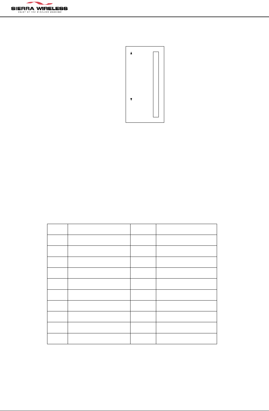
The Development Platform may be connected to a PC in a dual UART configuration as
illustrated below.
Host PC
A
B
COM
COM
Dev Board
2
1
UART
UART
Dual RS232
Configuration
Control Channel
Data Channel
Note that “COM A” and “COM B” labels are used on the host PC in the above diagram. This is
to identify the physical COM ports and should not be confused with the COM port number
assigned by Windows.

EM DEVELOPMENT PLATFORM Users Guide ver 0.6
CONFIDENTIAL AND PROPRIETARY PAGE 10
4 DEVELOPMENT PLATFORM HARDWARE
The Development Platform utilizes a number of switches for various controls and configuration
options. This section discusses these switches, LED indicators and the various Development
Platform headers and connectors.
4.1 Modes of Operation
The Development Platform supports two modes of operation, Standalone Mode and Extender
Mode. In both modes of operation, the wireless modem module is mounted on the
Development Platform. Standalone Mode allows for operation of the module independent of the
target host system while Extender Mode assists with hardware and software integration of the
module into the target host system.
Please refer to the table at the end of this section for the switch settings for each mode.
4.1.1 Standalone Mode
Standalone Mode is intended for product evaluation and software development independent of
the target host system. In Standalone Mode, a PC or other host can communicate with the
Development Platform via serial ports. Standalone Mode also supports audio test capability via
a 2.5mm headset jack.
4.1.2 Extender Mode
In Extender Mode, a “dummy” module is installed in the target host in place of the wireless
modem module. This “dummy” module provides a flex cable connection to the Development
Platform. In this arrangement, the wireless modem module on the Development Platform is
powered and controlled by the target host. This mode of operation allows for probing a number
of the signals on the module host interface connector. Additionally the serial ports can be
configured to allow monitoring of RX and TX communication directions for both ports using a
serial port analyzer.
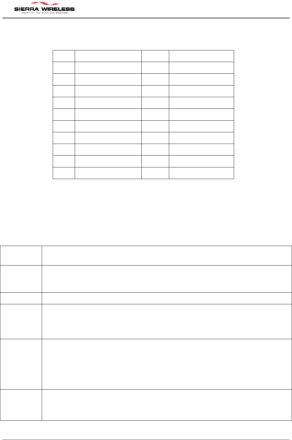
Switch Standalone Mode Extender Mode Serial Port
Analysis
SW2-1 ON OFF OFF
SW2-4 OFF ON OFF
EM DEVELOPMENT PLATFORM Users Guide ver 0.6
CONFIDENTIAL AND PROPRIETARY PAGE 11
4.1.3 LED indicators
CN18 sockets10 segment LED bar (Lumex part # SSA-LXB10IW-GF/LP)
Each segment is related to an IO signal as shown in the table below. The LED lights up when
the signal is in the low state – off when the signal is in the high state.
Pin # Signal Name
1 DTR1
2 CD1
3 DSR1
4 MODULE_WAKE
5 HOST_WAKE
6 HOST_STATUS
7 RESET_RADIO
8 RESET_OUT
9 VCC_RADIO
10 VCC_BRD
4.2 Powering the Development Platform
There are two options for powering the Development Platform, using an AC “wall-cube” or DC
power from an external power supply.
4.2.1 AC Wall Cube Power
When using the AC “wall-cube”, the DC output jack from the wall-cube will connect to the “DC
Input” back on the Development Platform.
If the “wall-cube” supplied with the Dev Platform is not suitable, another wall-cube may be used
so long as it has a 5V output rated for at least 2 Amps with the jack barrel exterior grounded and
5V on the barrel interior.
The table below shows the required switch settings when using wall-cube power:
Switch Position
SW2-8 ON
EM DEVELOPMENT PLATFORM Users Guide ver 0.6
CONFIDENTIAL AND PROPRIETARY PAGE 12
4.2.2 DC Power
If using a DC power source without a jack connector, the DC voltage must be between 3.6V and
4.2V and rated for at least 2 Amps. The DC voltage must be connected to the Development
Platform on TP1 and ground must be connected on TP3.
The table below shows the required switch settings when using wall-cube power:
Switch Position
SW2-8 OFF
4.3 Audio Testing
The Development Platform provides two methods of audio testing, a 2.5mm headset jack for a
hands free headset and an RJ11 connector for a standard telephone handset.
4.3.1 Using a Headset
The Development Platform has a 2.5mm headset jack for a cellphone headset.
4.3.2 Using a Headset
MIC Bias Voltage – When using a headset in Standalone Mode or if the host does not provide a
MIC bias voltage, set SW3-1 to the ON position, otherwise this switch should be set to the OFF
position. Note that the default audio gains of the modem are set for use with a host front end
which contains additional gains in the transmit path (20dB). For this reason the audio will be
very faint while using the headset in standalone mode – unless additional gains are added to
the modem transmit path using directed test scripts.
4.4 External Interfaces
4.4.1 UART1 - DB9
Used to access the EM3420 wireless modem module UART1, RS-232 compatible
Signals from the module connector to this DB9 will be level shifted using an RS-232 transceiver.
AMP, Part #: 747844-2 (or equivalent)
Pin # Signal Name
1 CD
2 RXD
3 TXD
4 DTR
5 GND
EM DEVELOPMENT PLATFORM Users Guide ver 0.6
CONFIDENTIAL AND PROPRIETARY PAGE 13
6 DSR
7 RTS
8 CTS
9 RI
4.4.2 UART2 - DB9
Used to access the EM3420 wireless modem module UART2. RS-232 compatible 2 wire or 4-
wire interface.
Signals from the EM 3420 wireless modem module connector to this DB9 will be level shifted
using an RS-232 transceiver.
AMP, Part #: 747844-2 (or equivalent)
Pin # Signal Name
1 NC
2 RXD
3 TXD
4 NC
5 GND
6 NC
7 RTS
8 CTS
9 NC
4.4.3 DC Jack
Connects to the provided AC wall adapter.
Switchcraft, Part #: RAPC712
4.4.4 Headset Jack
This is a standard 2.5mm headset jack.
Hosiden, Part #: HSJ1621-01901
Pin # Signal Name
1 GND
2 MIC_P
3 SPK_P
4 MIC_DET
5 SPK_DET
EM DEVELOPMENT PLATFORM Users Guide ver 0.6
CONFIDENTIAL AND PROPRIETARY PAGE 14
Below is the schematic representation of the headset jack:
HSJ1621_01901
(HOSIDEN)
2
4
5
3
1
4.5 Debug Headers
Internal to the Development Platform are two standard 2-row 0.1” x 0.1” headers that can be
used for connecting logic analyzer or scope probes to.
4.5.1 CN2 - Audio Test Points
Pin # Signal Name Pin # Signal Name
1 11 RTS2
2 12 PCM_FRAME
3 13 PCM_DIN
4 TXD1 14 PCM_CLK
5 RXD1 15 PCM_DOUT
6 CTS1 16 RI1
7 RTS1 17 DTR1
8 TXD2 18 CD1
9 RXD2 19 DSR1
10 CTS2 20 GND
EM DEVELOPMENT PLATFORM Users Guide ver 0.6
CONFIDENTIAL AND PROPRIETARY PAGE 15
4.5.2 CN12 - Control/Status Signal Test Points
Pin # Signal Name Pin # Signal Name
1 11 HOST_STATUS
2 VCC_RADIO 12 RESET_OUT
3 13 MIC_P
4 VCC_BB 14 SPK_P
5 15 MIC_N
6 VBATT 16 SPK_N
7 ON/OFF 17 HOST_WAKE
8 RADIO_RESET 18
9 MODULE_WAKE 19
10 20 GND
4.6 DIP Switch Settings
4.6.1
Switch 2 (SW2)
Switch
Position Function
1 UART RX Enable – This switch controls the receiver output enable for the on-
board RS232 level shifters. It must be set to the ON position for Standalone
Mode and must be set to the OFF position for Extender Mode.
2 NA
3 MODULE ON/OFF – This switch is used to turn the module on. Turning switch to
OFF position turns modem on. Turning switch to ON position turns modem off.
This switch is only used in standalone mode to control modem power state. In the
extender mode this switch should be set to OFF.
4 UART Shutdown - This switch controls the power to the on-board RS232 level
shifters. Turning switch to OFF position enables the UART transmit. Turning
switch to ON position disables UART transmit (towards PC). It must be set to the
OFF position for Standalone Mode and can be set to the ON position for Extender
Mode if serial port analysis isn’t required. For serial port analysis while in
Extender mode – set this switch to OFF.
5 Flex_ON/OFF (INV). This switch is only used when modem is connected to a
host (extender mode). This switch is only set to ON with a host with active low
enable for modem turn on control. The modem power up control is active high –
so this switch inverts the logic of the power enable control from the host. In

EM DEVELOPMENT PLATFORM Users Guide ver 0.6
CONFIDENTIAL AND PROPRIETARY PAGE 16
standalone mode (default) always set this switch to OFF.
6 FLEX_ON/OFF – This switch passes the target adapter ON/OFF control directly
to the modem on board. Set this switch to ON only for the extender mode with a
host with active high enable for modem turn on control. In standalone mode
always set this switch to OFF.
7 NA
8 On-board VBAT Regulator Enable – This switch controls the on-board regulator
for the module’s VBAT power. This switch is only set to ON when using the wall
cube power supply to power the modem. If taking power from the host system in
extender or mode – set this switch to OFF.
9 HOST_STAT Control – Set this switch to the OFF position to enable Standalone
Mode (must be used with MDL_WAKE).
10 MDL_WAKE Control – Set to this switch to the ON position for Standalone Mode.
Tells module on power-up to run in standalone mode (Must be used with
HOST_STAT). Set to OFF for extender mode.
EM DEVELOPMENT PLATFORM Users Guide ver 0.6
CONFIDENTIAL AND PROPRIETARY PAGE 17
Switch 3 (SW3)
Switch
Position Function
1 MIC BIAS Control – This switch is used to enable an onboard mic bias for the
headset. Turn to ON position to enable bias at headset microphone. Turn to OFF
position to disable bias. Turn to OFF during extender mode.
2 Test Switch – turn to OFF position
3 Test Switch – turn to OFF position
4 Test Switch – turn to OFF position
5 Test Switch – turn to OFF position
6 Test Switch – turn to OFF position
7 NA
8,9,10 8,9,10 are used for extender mode. For standalone mode simply set all to OFF
position. These switches determine whether the real modem on the comm. board
is powered by the board itself (wall cube or DC power) or takes power from the
host system.
For host power set 8,9,10 to OFF, ON, ON
For on board power set 8,9,10 to OFF, OFF, OFF.
Most common configuration for extender mode is to use host power.
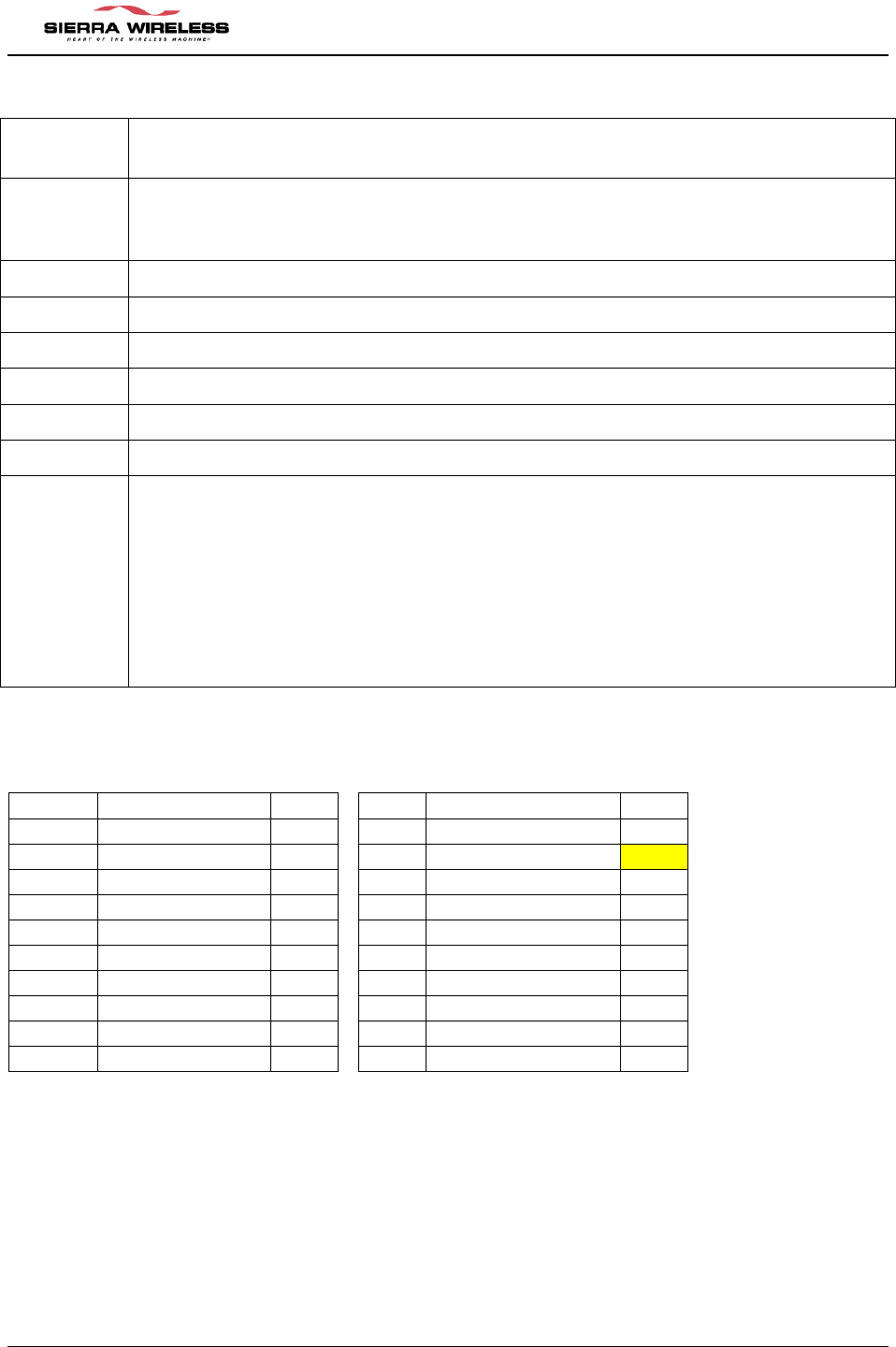
Default DIP switch settings
(standalone)
SW3
Title Default
SW2
Title Default
10
MOD_RF OFF 10
Module Wake ON
9
MOD_RF ON 9
Host Stat OFF
8
MOD_BB ON 8
Wall Pwr Enable ON
7
NC OFF 7
NC OFF
6
Test OFF 6
FLEX ON/OFF OFF
5
Test OFF 5
FLEX ON/OFF inv OFF
4
Test OFF 4
UART_SD OFF
3
Test OFF 3
Module On OFF
2
Test OFF 2
NC OFF
1
MIC BIAS OFF 1
UART Enable ON

EM DEVELOPMENT PLATFORM Users Guide ver 0.6
CONFIDENTIAL AND PROPRIETARY PAGE 18
5 RF INTEGRATION
5.1 Introduction
This chapter covers information related to the radio frequency (RF) integration of the EM3420 wireless
modem module. The modem’s RF performance specifications are noted below.
Maximum Transmit Power: PCS: +24.0 dBm (251 mW)
Cellular: +24.0 dBm (251mW)
Receiver Sensitivity: PCS: >-106
Cellular: >-106
Receiver Band: PCS: 1930 to 1990 MHz
Cellular: 869 to 894 MHz
Transmit Band PCS: 1851 to 1910 MHz
Cellular: 824 to 849 MHz
Channel Spacing: 1.25 MHz
GPS Band 1575.24Mhz
5.2 RF Connection
The antenna connection point on the EM3420 wireless modem can be attached in several ways.
The wireless modem antenna connection can be made with coaxial cable using the Hirose UFL
or Murata CSG series coaxial cable connectors, a custom design antenna touch pad, or by
soldering the antenna coaxial cable directly to the EM3420 antenna contact. The direct solder
method may void some portions of the warranty. Check with your sales associate for
clarification if this method of attachment is required. Any Coaxial connection between the
EM3420 wireless modem module and the antenna requires the antenna to be correctly matched
to 50.
5.3 Ground Plane Isolation
Ground loops must be avoided between the host connector and the antenna.
The coaxial cable connecting the module to the antenna carries the ground connection. There
must be an electrical isolation between the ground plane at the antenna and the ground plane
used by the modem.
If these two ground planes were not isolated, there would be a ground loop from the modem
through the coaxial cable and back through the ground plane to the modem’s own ground. This
must be avoided.
If your integration uses the device’s case as part of the ground connection, then the external
antenna connection must be isolated from the case to avoid creating a ground loop. However,
in vehicle integrations, it is acceptable to have a remote antenna ground connection to the
vehicle chassis.

EM DEVELOPMENT PLATFORM Users Guide ver 0.6
CONFIDENTIAL AND PROPRIETARY PAGE 19
5.4 Antenna and Cabling
After determining the antenna connection method the selection of antenna and cabling must be
made.
5.4.1 Matching Antenna and Cable
Matching antenna-gain and cable loss is critical to effective RF performance.
For proper matching, the antenna along with any associated matching should have a nominal
impedance of 50 with a return loss -10 dB between 824 – 894 MHz, 1575.24MHz, and 1851
– 1990 MHz. Overall system antenna gain, with cable loss, should be 0 dBi and +6 dBi.
Keep in mind that your achieved value will have an impact on radiated power and the FCC
MPE/SAR test results.
5.4.2 Antenna Options
There are many antenna vendors who are producing dual-band antennas that may work with
the EM3420 wireless modem module. Custom antenna design is also possible but requires a
skilled RF engineer to ensure that the RF performance is maintained.
Location of the antenna can also have an impact on RF performance of the EM3420 wireless
modem module. The modem it’s itself is shielded to prevent interference in most applications,
but this does not mean that antenna placement can be ignored.
5.4.3 Cables
Any connecting cables between the modem and the antenna (if required) must be 50.
Mismatching the impedance of the EM3420 wireless modem module will result in a significant
reduction in RF performance.
5.5 Interference and Sensitivity
There are several sources of interference that could impact the RF performance of the EM3420
wireless modem module. A few are discussed below.
Sierra Wireless America offers modem OTA (Over-The-Air) sensitivity testing and desense
investigation. Most carriers require a certain level of receiver performance in order for the
device to function properly on their network. Although the EM3420 wireless modem module has
been designed to meet these carrier requirements it is still susceptible to various performance
inhibitors.
5.5.1 Power Supply Noise
Noise in the power supply can lead to noise in the RF signal. The specification for power supply
ripples should be no more than 100 mVp-p 1 Hz to 100 kHz.

EM DEVELOPMENT PLATFORM Users Guide ver 0.6
CONFIDENTIAL AND PROPRIETARY PAGE 20
5.5.2 Device Generated RF
All electronic computing devices generate radio frequency (RF) interference. You should pay
particular attention to RF noise as it can impact the receive sensitivity of the EM3420 wireless
modem.
The proximity of host electronics to the antenna can have an adverse effect on the radio’s
sensitivity. There are many high-speed devices (in particular the processor itself) running at
frequencies of 10’s of MHz. These signals generate higher order harmonics due to the rapid
rise and fall times. These harmonics often fall within the operating frequency band of the
EM3420 wireless modem module and cause a decrease in receiver sensitivity.
For example, if we have a sub-system running at 40 MHz, the 22nd harmonic falls at 880 MHz,
which is within the cellular receive frequency band. In reality there are usually numerous
interfering frequencies and harmonics. The net effect can be a series of desense receive
channels. Most device designers are familiar with having to pay attention to radiated emissions
in order to meet the FCC Part 15 rules. The major culprits in causing RF desense are found to
be the microprocessor and memory, display panel and display drivers, and switching mode
power supplies.
Some or all of the following techniques may be followed to mitigate this type of RF desense:
• Keep the antenna as remote as possible. By moving the antenna further away from
the source of the interference, the effect of the interference may be reduced. The
drawback of this approach is the modem may be less convenient to use.
• Shield the host device. The EM3420 wireless modem module itself is well shielded
to avoid interference, however it is not practical to shield the antenna for obvious
reasons. In most instances it is necessary to employ shielding over the worst radiating
elements of the host device (such as the main processor) to reduce such emissions.
• Discrete filtering may also be used on low frequency lines to filter out unwanted high
order harmonic energy.
• PCB layout. Use multi-layer PCB’s to form shielding layers around high-speed clock
traces.
Effective integrators of wireless communication devices inside of computing devices are likely to
make use of good design practices coupled with investigative techniques to locate and isolate
source of localized interference. It is important to carry out these investigations as early as
possible in the design cycle.
The EM 3420 wireless modem module radio circuits use a number of intermediate frequency
(IF) stages. The following specific frequencies should be avoided or suppressed in the host
device to maintain the best sensitivity performance:
• 183.6 MHz
• 228.6 MHz
• 263.6 MHz

EM DEVELOPMENT PLATFORM Users Guide ver 0.6
CONFIDENTIAL AND PROPRIETARY PAGE 21
5.5.3 Hearing Aid Considerations
In addition to outside frequencies interfering with the modem’s sensitivity, the modem itself can
cause noise in hearing aids due to the keying of the transmitter.
Most digital wireless technologies do not transmit radio frequencies continuously. They transmit
in bursts, usually of specific durations, which are often described in terms of RF switching
frequencies.
Unfortunately, most hearing aids are not immune to RF; they try to rectify the switching
frequencies into audio. This causes unpleasant noise for hearing aid users in close proximity to
transmitters, as is the case with digital wireless phones.