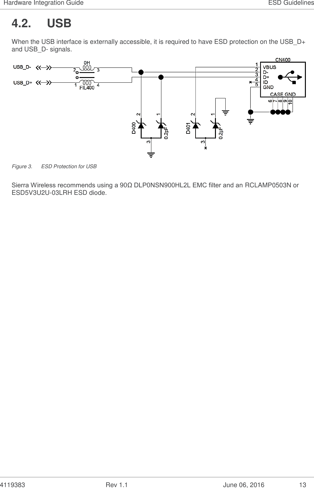
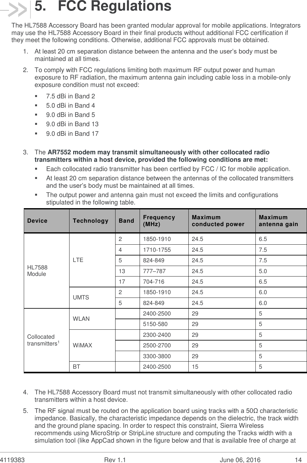
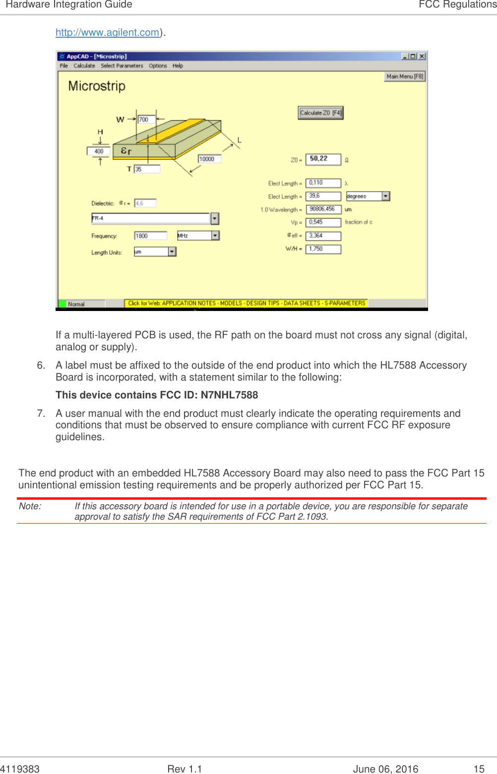
Sierra Wireless HL7588 Wireless Module User Manual Hardware Integration Guide

Sierra Wireless Inc. Wireless Module Hardware Integration Guide

Contents

HL7588 Accessory Board - Hardware Integration Guide - Rev1.1

    4119383 1.1 June 06, 2016  AirPrime HL7588 Accessory Board Hardware Integration Guide
 4119383  Rev 1.1  June 06, 2016  2 Hardware Integration Guide  Important Notice Due to the nature of wireless communications, transmission and reception of data can never be guaranteed. Data may be delayed, corrupted (i.e., have errors) or be totally lost. Although significant delays or losses of data are rare when wireless devices such as the Sierra Wireless modem are used in a normal manner with a well-constructed network, the Sierra Wireless modem should not be used in situations where failure to transmit or receive data could result in damage of any kind to the user or any other party, including but not limited to personal injury, death, or loss of property. Sierra Wireless accepts no responsibility for damages of any kind resulting from delays or errors in data transmitted or received using the Sierra Wireless modem, or for failure of the Sierra Wireless modem to transmit or receive such data. Safety and Hazards Do not operate the Sierra Wireless modem in areas where cellular modems are not advised without proper device certifications. These areas include environments where cellular radio can interfere such as explosive atmospheres, medical equipment, or any other equipment which may be susceptible to any form of radio interference. The Sierra Wireless modem can transmit signals that could interfere with this equipment. Do not operate the Sierra Wireless modem in any aircraft, whether the aircraft is on the ground or in flight. In aircraft, the Sierra Wireless modem MUST BE POWERED OFF. When operating, the Sierra Wireless modem can transmit signals that could interfere with various onboard systems. Note:   Some airlines may permit the use of cellular phones while the aircraft is on the ground and the door is open. Sierra Wireless modems may be used at this time. The driver or operator of any vehicle should not operate the Sierra Wireless modem while in control of a vehicle. Doing so will detract from the driver or operator’s control and operation of that vehicle. In some states and provinces, operating such communications devices while in control of a vehicle is an offence. Limitations of Liability This manual is provided “as is”. Sierra Wireless makes no warranties of any kind, either expressed or implied, including any implied warranties of merchantability, fitness for a particular purpose, or noninfringement. The recipient of the manual shall endorse all risks arising from its use.   The information in this manual is subject to change without notice and does not represent a commitment on the part of Sierra Wireless. SIERRA WIRELESS AND ITS AFFILIATES SPECIFICALLY DISCLAIM LIABILITY FOR ANY AND ALL DIRECT, INDIRECT, SPECIAL, GENERAL, INCIDENTAL, CONSEQUENTIAL, PUNITIVE OR EXEMPLARY DAMAGES INCLUDING, BUT NOT LIMITED TO, LOSS OF PROFITS OR REVENUE OR ANTICIPATED PROFITS OR REVENUE ARISING OUT OF THE USE OR INABILITY TO USE ANY SIERRA WIRELESS PRODUCT, EVEN IF SIERRA WIRELESS AND/OR ITS AFFILIATES HAS BEEN ADVISED OF THE POSSIBILITY OF SUCH DAMAGES OR THEY ARE FORESEEABLE OR FOR CLAIMS BY ANY THIRD PARTY. Notwithstanding the foregoing, in no event shall Sierra Wireless and/or its affiliates aggregate liability arising under or in connection with the Sierra Wireless product, regardless of the number of events, occurrences, or claims giving rise to liability, be in excess of the price paid by the purchaser for the Sierra Wireless product. Customer understands that Sierra Wireless is not providing cellular or GPS (including A-GPS) services. These services are provided by a third party and should be purchased directly by the Customer.
 4119383  Rev 1.1  June 06, 2016  3 Hardware Integration Guide  SPECIFIC DISCLAIMERS OF LIABILITY: CUSTOMER RECOGNIZES AND ACKNOWLEDGES SIERRA WIRELESS IS NOT RESPONSIBLE FOR AND SHALL NOT BE HELD LIABLE FOR ANY DEFECT OR DEFICIENCY OF ANY KIND OF CELLULAR OR GPS (INCLUDING A-GPS) SERVICES. Patents This product may contain technology developed by or for Sierra Wireless Inc. This product includes technology licensed from QUALCOMM®. This product is manufactured or sold by Sierra Wireless Inc. or its affiliates under one or more patents licensed from InterDigital Group and MMP Portfolio Licensing. Copyright © 2016 Sierra Wireless. All rights reserved. Trademarks Sierra Wireless®, AirPrime®, AirLink®, AirVantage®, WISMO®, ALEOS® and the Sierra Wireless and Open AT logos are registered trademarks of Sierra Wireless, Inc. or one of its subsidiaries. Watcher® is a registered trademark of NETGEAR, Inc., used under license. Windows® and Windows Vista® are registered trademarks of Microsoft Corporation. Macintosh® and Mac OS X® are registered trademarks of Apple Inc., registered in the U.S. and other countries. QUALCOMM® is a registered trademark of QUALCOMM Incorporated. Used under license. Other trademarks are the property of their respective owners. Contact Information Sales Desk: Phone: 1-604-232-1488 Hours: 8:00 AM to 5:00 PM Pacific Time Contact: http://www.sierrawireless.com/sales Post: Sierra Wireless 13811 Wireless Way Richmond, BC Canada                      V6V 3A4 Technical Support: support@sierrawireless.com RMA Support: repairs@sierrawireless.com Fax: 1-604-231-1109 Web: http://www.sierrawireless.com/ Consult our website for up-to-date product descriptions, documentation, application notes, firmware upgrades, troubleshooting tips, and press releases: www.sierrawireless.com
 4119383  Rev 1.1  June 06, 2016  4 Hardware Integration Guide  Document History Version Date Updates 1.0 June 01, 2016 Creation 1.1 June 06, 2016 Removed Power Up Sequence
 4119383  Rev 1.1  June 06, 2016  5 Contents 1. INTRODUCTION .................................................................................................. 8 2. POWER INTERFACE ........................................................................................... 9 2.1. Power Supply .................................................................................................................... 9 2.2. Power Off Sequence ......................................................................................................... 9 2.3. Sleep Mode Management ................................................................................................. 9 3. RF INTERFACE .................................................................................................. 10 3.1. Supported RF Bands ....................................................................................................... 10 3.2. RF Connection ................................................................................................................. 10 3.3. RF Performances ............................................................................................................ 11 3.4. TX_ON Indicator .............................................................................................................. 11 4. ESD GUIDELINES .............................................................................................. 12 4.1. SIM Card ......................................................................................................................... 12 4.2. USB ................................................................................................................................. 13 5. FCC REGULATIONS ......................................................................................... 14 6. REFERENCES ................................................................................................... 16 6.1. Reference Documents ..................................................................................................... 16 6.2. Terms and Abbreviations................................................................................................. 16
 4119383  Rev 1.1  June 06, 2016  6 List of Figures Figure 1. TX_ON State During Transmission ................................................................................. 11 Figure 2. EMC and ESD Components Close to the SIM ................................................................ 12 Figure 3. ESD Protection for USB .................................................................................................. 13
 4119383  Rev 1.1  June 06, 2016  7 List of Tables Table 1. Power Supply .................................................................................................................... 9 Table 2. Supported Bands ............................................................................................................. 10 Table 3. RF Main Connection ........................................................................................................ 10 Table 4. RF Diversity Connection .................................................................................................. 10 Table 5. Conducted RX Sensitivity (dBm) ..................................................................................... 11 Table 6. TX_ON Indicator Description ........................................................................................... 11 Table 7. TX_ON Characteristics .................................................................................................... 11
 4119383  Rev 1.1  June 06, 2016  8 1.  Introduction The AirPrime HL7588 Accessory Board belongs to the AirPrime MC Series product family and provides data connectivity on wireless networks as listed in Table 2 Supported Bands.  The HL7588 Accessory Board supports a large variety of interfaces such as USB 2.0, UART, GPIOs, and SIM to provide customers with the highest level of flexibility in implementing high-end solutions.
 4119383  Rev 1.1  June 06, 2016  9 2.  Power Interface 2.1.  Power Supply The AirPrime HL7588 Accessory Board is supplied through the VBAT signal. Table 1.  Power Supply Pin Numbers Supply Minimum Typical Maximum 2, 24, 39, 41, 52 VBAT voltage (V) 3.2* 3.7 4.5 *    This value has to be guaranteed during the burst. Note:   Load capacitance for VBAT is around 32µF ± 20% embedded inside the accessory board. 2.2.  Power Off Sequence To power the HL7588 Accessory Board off: 1. Put the accessory board in low power mode (LPM) by sending either AT+KSLEEP=1 or AT+CPWROFF=1. 2. Wait for at least 10 seconds. 3. Remove the power supply to VBAT. 2.3.  Sleep Mode Management Use AT+KSLEEP=1 to allow the accessory board to automatically enter sleep mode while the USB interface is in use. When AT+KSLEEP=2, the accessory board will never enter sleep mode.
 4119383  Rev 1.1  June 06, 2016  10 3.  RF Interface The RF interface of the HL7588 Accessory Board allows the transmission of RF signals. This interface has a 50Ω nominal impedance. 3.1.  Supported RF Bands The HL7588 Accessory Board supports the RF bands listed in the table below. Table 2.  Supported Bands  RF Band Transmit Band (Tx) Receive Band (Rx) Maximum Output Power LTE B2 1850 to 1910 MHz 1930 to 1990 MHz 22.5 dBm (+/- 2dBm) Class 3bis LTE B4 1710 to 1755 MHz 2110 to 2155 MHz 22.5 dBm (+/- 2dBm) Class 3bis LTE B5 824 to 849 MHz 869 to 894 MHz 22.5 dBm (+/- 2dBm) Class 3bis LTE B13 777 to 787 MHz 746 to 756 MHz 22.5 dBm (+/- 2dBm) Class 3bis LTE B17 704 to 716 MHz 734 to 746 MHz 22.5 dBm (+/- 2dBm) Class 3bis UMTS B2 1850 to 1910 MHz 1930 to 1990 MHz 22.5 dBm (+/- 2dBm) Class 3bis UMTS B5 824 to 849 MHz 869 to 894 MHz 22.5 dBm (+/- 2dBm) Class 3bis 3.2.  RF Connection A 50Ω stripline can be used to connect to standard RF connectors such as SMA, UFL, etc. for antenna connection. Table 3.  RF Main Connection RF Signal Impedance VSWR Rx (max) VSWR Tx (max) RF_MAIN 50Ω 1.5:1 1.5:1 Table 4.  RF Diversity Connection RF Signal Impedance VSWR Rx (max) VSWR Tx (max) RF_DIV 50Ω 1.5:1 ---
 4119383  Rev 1.1  June 06, 2016  11 Hardware Integration Guide RF Interface 3.3.  RF Performances RF performances are compliant with 3GPP recommendation TS 36.101. Note:   Values in the table below are preliminary and subject to change. Table 5.  Conducted RX Sensitivity (dBm) Frequency Band  Primary (Typical) Secondary (Typical) SIMO (Typical) LTE B2 Full RB; BW: 20 MHz* -92.5 -92.5 -95.5 LTE B4 Full RB; BW: 20 MHz* -94.5 -94.5 -97.5 LTE B5 Full RB; BW: 10 MHz* -97.5 -98.5 -101.5 LTE B13 Full RB; BW: 10 MHz* -97.5 -98.5 -101.5 LTE B17 Full RB; BW: 10 MHz* -97.5 -98.5 -101.5 *    Sensitivity values scale with bandwidth: x_MHz_Sensitivity = 10 MHz_Sensitivity – 10*log (10 MHz/x_MHz) 3.4.  TX_ON Indicator The AirPrime HL7588 Accessory Board provides a signal, 2G_TX_ON, for TX indication. 2G_TX_ON is a 2.3V signal and its status signal depends on the accessory board’s transmitter state. Refer to the following table for the status of the 2G_TX_ON signal depending on the HL7588 Accessory Board’s state. Table 6.  TX_ON Indicator Description Pin Number Signal Name Function I/O type Power Supply Domain 42 2G_TX_ON TX indicator O 2.3V Table 7.  TX_ON Characteristics Parameter Minimum Typical Maximum Tadvance 30µs   Tdelay  10µs  TX_ONVBATT_PAT durationT advance T delayVoltage drop Figure 1.  TX_ON State During Transmission
 4119383  Rev 1.1  June 06, 2016  12 4.  ESD Guidelines 4.1.  SIM Card Decoupling capacitors must be added according to the drawings below as close as possible to the SIM card connectors on UIM1_CLK, UIM1_RST, UIM1_VCC and UIM1_DATA signals to avoid EMC issues and to comply with the requirements of ETSI and 3GPP standards covering the SIM electrical interface. A typical schematic including SIM detection is provided below.  Figure 2.   EMC and ESD Components Close to the SIM
 4119383  Rev 1.1  June 06, 2016  13 Hardware Integration Guide ESD Guidelines 4.2.  USB When the USB interface is externally accessible, it is required to have ESD protection on the USB_D+ and USB_D- signals.  Figure 3.  ESD Protection for USB Sierra Wireless recommends using a 90Ω DLP0NSN900HL2L EMC filter and an RCLAMP0503N or ESD5V3U2U-03LRH ESD diode.
 4119383  Rev 1.1  June 06, 2016  14 5.  FCC Regulations The HL7588 Accessory Board has been granted modular approval for mobile applications. Integrators may use the HL7588 Accessory Board in their final products without additional FCC certification if they meet the following conditions. Otherwise, additional FCC approvals must be obtained. 1. At least 20 cm separation distance between the antenna and the user’s body must be maintained at all times. 2. To comply with FCC regulations limiting both maximum RF output power and human exposure to RF radiation, the maximum antenna gain including cable loss in a mobile-only exposure condition must not exceed:  7.5 dBi in Band 2  5.0 dBi in Band 4  9.0 dBi in Band 5  9.0 dBi in Band 13  9.0 dBi in Band 17  3. The AR7552 modem may transmit simultaneously with other collocated radio transmitters within a host device, provided the following conditions are met:  Each collocated radio transmitter has been certfied by FCC / IC for mobile application.  At least 20 cm separation distance between the antennas of the collocated transmitters and the user’s body must be maintained at all times.  The output power and antenna gain must not exceed the limits and configurations stipulated in the following table.  Device Technology Band Frequency (MHz) Maximum conducted power Maximum antenna gain HL7588 Module LTE 2 1850-1910 24.5 6.5  4 1710-1755 24.5 7.5  5 824-849 24.5 7.5  13 777–787 24.5 5.0  17 704-716 24.5 6.5  UMTS 2 1850-1910 24.5 6.0  5 824-849 24.5 6.0  Collocated transmitters1 WLAN  2400-2500 29 5  5150-580 29 5 WiMAX  2300-2400 29 5  2500-2700 29 5  3300-3800 29 5 BT  2400-2500 15 5  4. The HL7588 Accessory Board must not transmit simultaneously with other collocated radio transmitters within a host device. 5. The RF signal must be routed on the application board using tracks with a 50Ω characteristic impedance. Basically, the characteristic impedance depends on the dielectric, the track width and the ground plane spacing. In order to respect this constraint, Sierra Wireless recommends using MicroStrip or StripLine structure and computing the Tracks width with a simulation tool (like AppCad shown in the figure below and that is available free of charge at
 4119383  Rev 1.1  June 06, 2016  15 Hardware Integration Guide FCC Regulations http://www.agilent.com).    If a multi-layered PCB is used, the RF path on the board must not cross any signal (digital, analog or supply).  6. A label must be affixed to the outside of the end product into which the HL7588 Accessory Board is incorporated, with a statement similar to the following: This device contains FCC ID: N7NHL7588 7. A user manual with the end product must clearly indicate the operating requirements and conditions that must be observed to ensure compliance with current FCC RF exposure guidelines.  The end product with an embedded HL7588 Accessory Board may also need to pass the FCC Part 15 unintentional emission testing requirements and be properly authorized per FCC Part 15. Note:   If this accessory board is intended for use in a portable device, you are responsible for separate approval to satisfy the SAR requirements of FCC Part 2.1093.
 4119383  Rev 1.1  June 06, 2016  16 6.  References 6.1.  Reference Documents [1] AirPrime HL7588 Accessory Board Product Technical Specification Reference number: 4119052 6.2.  Terms and Abbreviations Abbreviation Definition ADC Analog to Digital Converter AGC Automatic Gain Control AT Attention (prefix for modem commands) CDMA Code Division Multiple Access CF3 Common Flexible Form Factor CLK Clock CODEC Coder Decoder CPU Central Processing Unit DAC Digital to Analog Converter DTR Data Terminal Ready EGNOS European Geostationary Navigation Overlay Service EMC Electromagnetic Compatibility EMI Electromagnetic Interference EN Enable ESD Electrostatic Discharges ETSI European Telecommunications Standards Institute FDMA Frequency-division multiple access GAGAN GPS aided geo augmented navigation GLONASS Global Navigation Satellite System  GND Ground GNSS Global Navigation Satellite System GPIO General Purpose Input Output GPRS General Packet Radio Service GSM Global System for Mobile communications Hi Z High impedance (Z) IC Integrated Circuit IMEI International Mobile Equipment Identification I/O Input / Output LED Light Emitting Diode LNA Low Noise Amplifier MAX Maximum MIN Minimum
 4119383  Rev 1.1  June 06, 2016  17 Hardware Integration Guide References Abbreviation Definition MSAS Multi-functional Satellite Augmentation System N/A Not Applicable PA Power Amplifier PC Personal Computer PCB Printed Circuit Board PCL Power Control Level PLL Phase Lock Loop PWM Pulse Width Modulation QZSS Quasi-Zenith Satellite System RF Radio Frequency RFI Radio Frequency Interference RMS Root Mean Square RST Reset RTC  Real Time Clock RX Receive  SCL Serial Clock SDA Serial Data SIM Subscriber Identification Module SMD Surface Mounted Device/Design SPI Serial Peripheral Interface SW Software PSRAM Pseudo Static RAM TBC To Be Confirmed TBD To Be Defined TP Test Point TX Transmit TYP Typical UART Universal Asynchronous Receiver-Transmitter UICC Universal Integrated Circuit Card USB Universal Serial Bus UIM User Identity Module VBATT Main Supply Voltage from Battery or DC adapter VSWR Voltage Standing Wave Ratio WAAS Wide Area Augmentation System

Navigation menu