Sierra Wireless HL7748 HL7748 module User Manual
Sierra Wireless Inc. HL7748 module
UserManual.wiki
>
Sierra Wireless
>
HL7748 User Manual
User manual
Navigation menu
Upload a User Manual
Namespaces
Wiki Guide
HTML
PDF
Info
Views
User Manual
Discussion / Help
Navigation

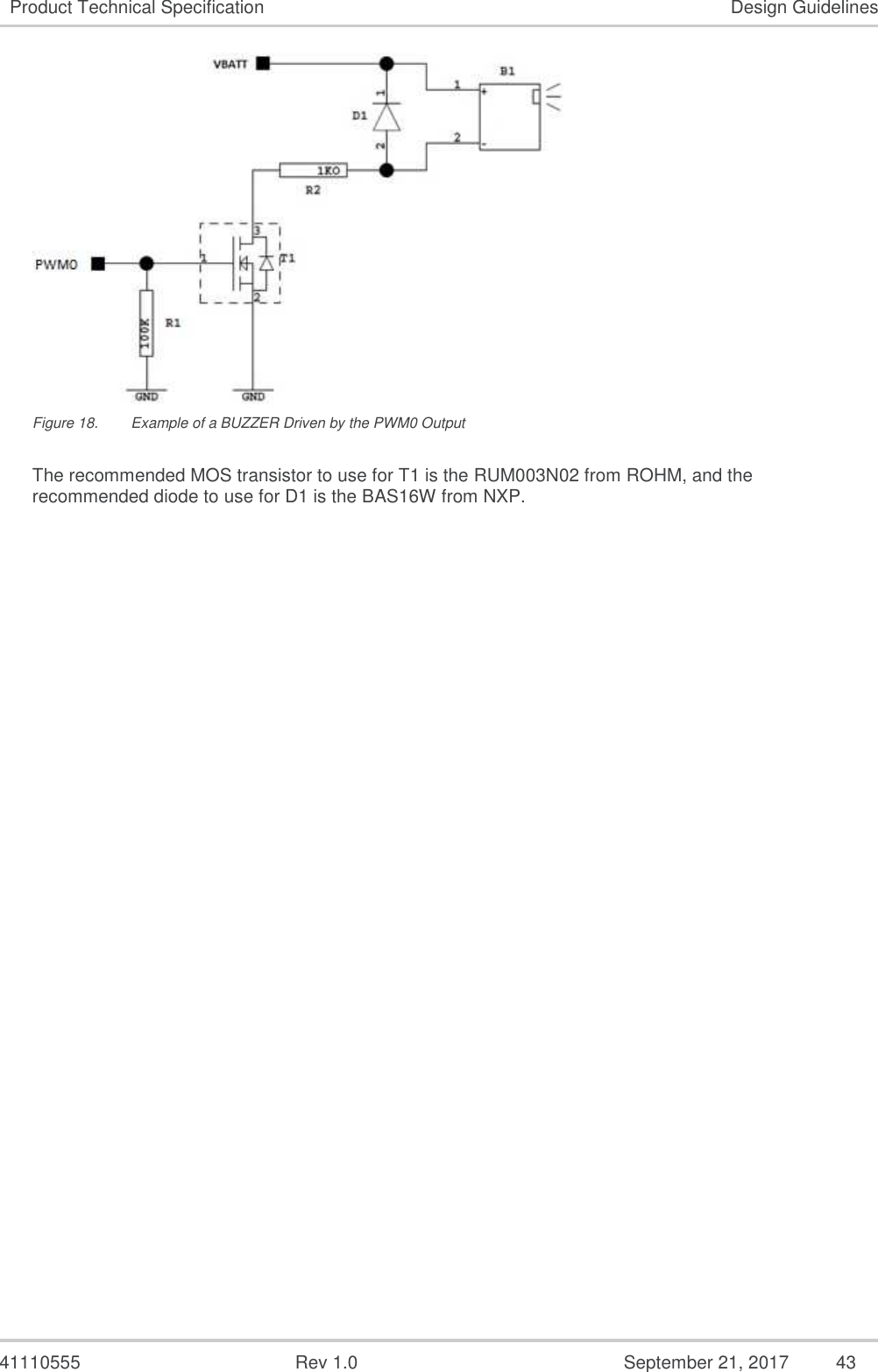
![41110555 Rev 1.0 September 21, 2017 16 Product Technical Specification Introduction 1.8.2. Regulatory The AirPrime HL7718 and HL7748 modules will be compliant with FCC regulations, while the AirPrime HL7749 module will be compliant with RCM regulations. 1.8.3. RoHS Directive Compliant The AirPrime HL77xx modules are compliant with RoHS Directive 2011/65/EU which sets limits for the use of certain restricted hazardous substances. This directive states that “from 1st July 2006, new electrical and electronic equipment put on the market does not contain lead, mercury, cadmium, hexavalent chromium, polybrominated biphenyls (PBB) or polybrominated diphenyl ethers (PBDE)”. 1.8.4. Disposing of the Product This electronic product is subject to the EU Directive 2012/19/EU for Waste Electrical and Electronic Equipment (WEEE). As such, this product must not be disposed of at a municipal waste collection point. Please refer to local regulations for directions on how to dispose of this product in an environmental friendly manner. 1.9. References [1] AirPrime HL Series Customer Process Guidelines Reference Number: 4114330 [2] AirPrime HL77xx AT Commands Interface Guide Reference Number: 41110842 [3] AirPrime HL Series Development Kit User Guide Reference Number: 4114877](https://usermanual.wiki/Sierra-Wireless/HL7748/User-Guide-3636301-Page-16.png)
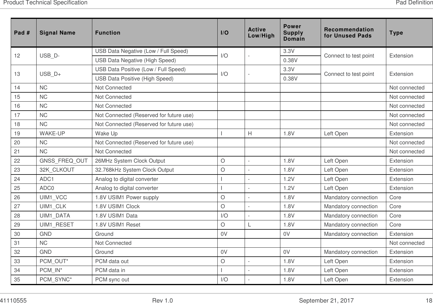
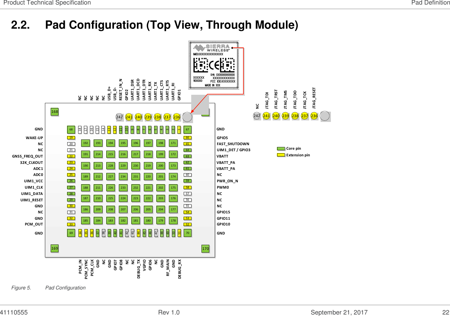
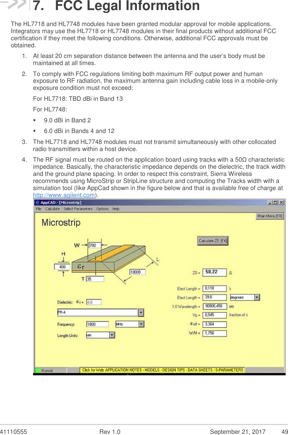
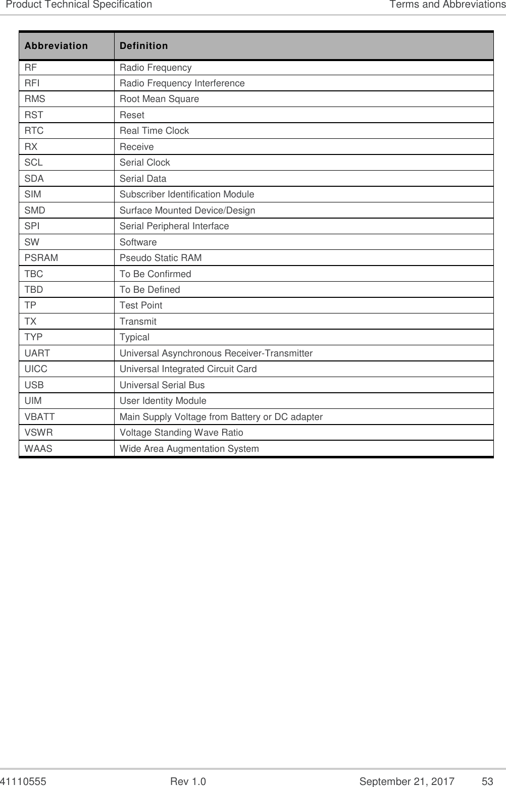
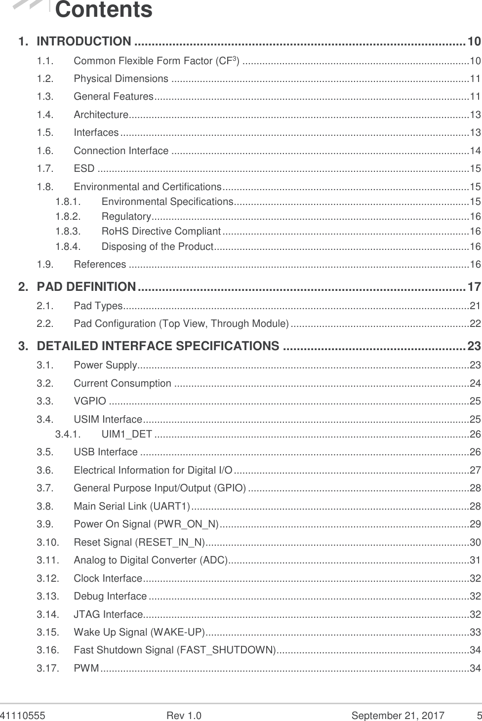
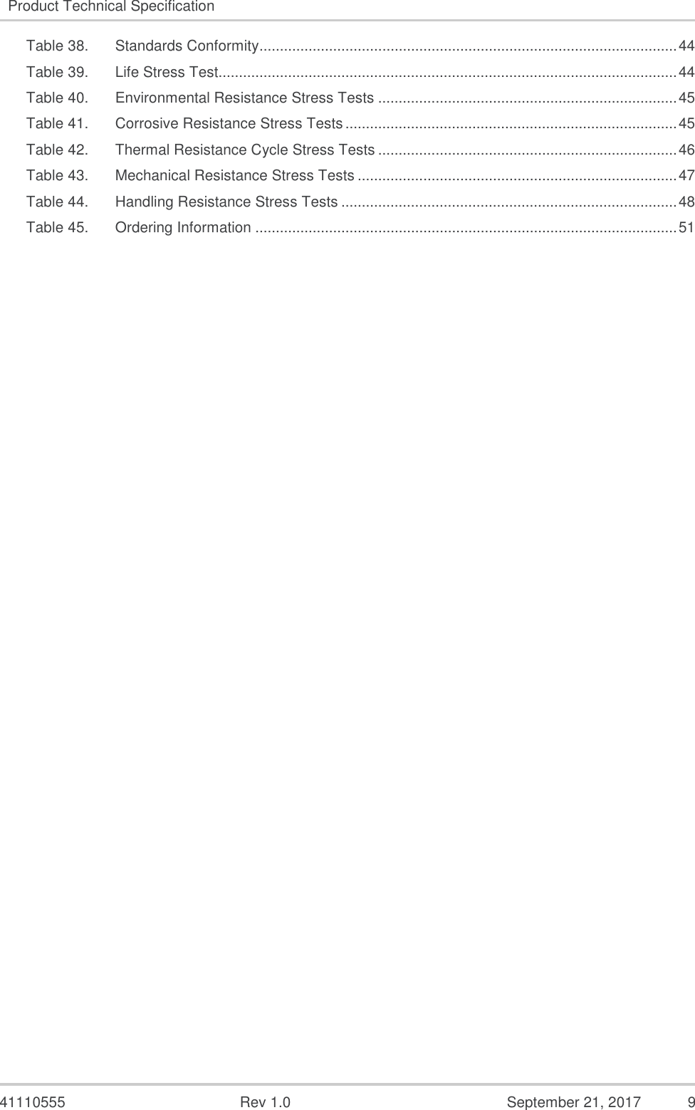
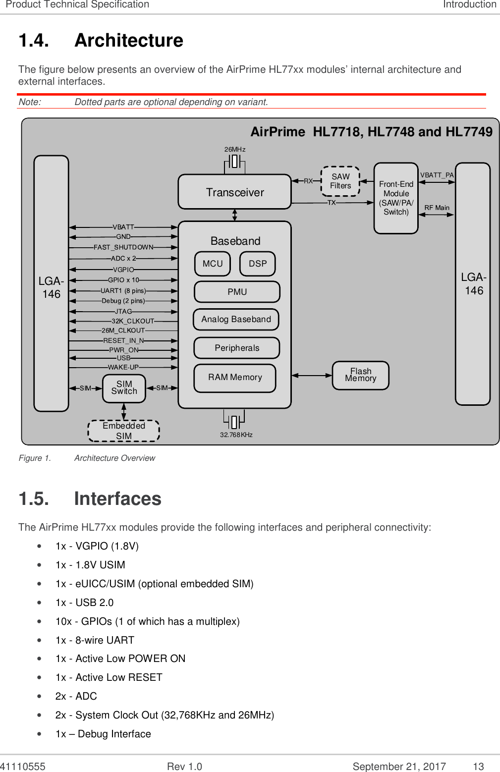
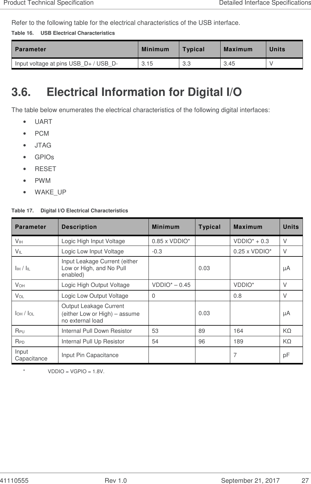
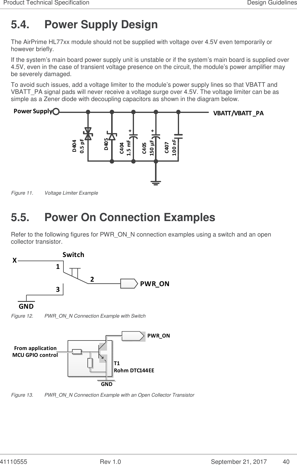
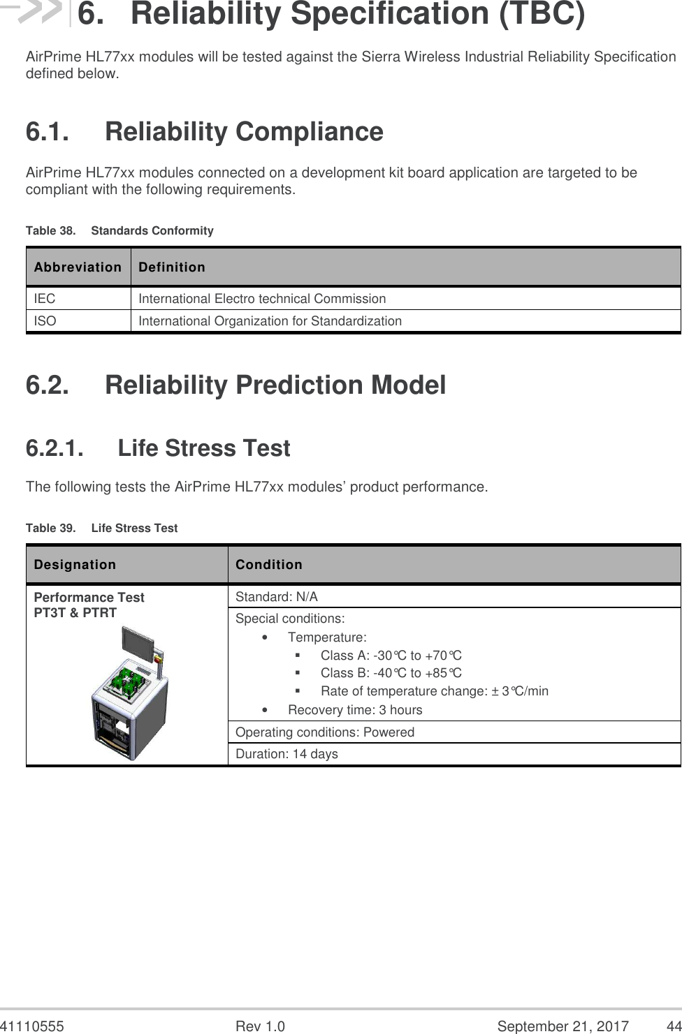
![41110555 Rev 1.0 September 21, 2017 26 Product Technical Specification Detailed Interface Specifications Table 13. USIM1 Pad Description Pad Number Signal Name Description Multiplex 26 UIM1_VCC 1.8V USIM1 Power supply 27 UIM1_CLK 1.8V USIM1 Clock 28 UIM1_DATA 1.8V USIM1 Data 29 UIM1_RESET 1.8V USIM1 Reset 64 UIM1_DET / GPIO3 1.8V USIM1 Detection GPIO3 Refer to the following table for the electrical characteristics of the USIM1 interface. Table 14. USIM1 Electrical Characteristics Parameter Minimum Typical Maximum Remarks UIM1 Interface Voltage (V) (VCC, CLK, IO, RESET) - 1.80 - The appropriate output voltage is auto detected and selected by software. UIM1 Detect - 1.80 - High active UIM1_VCC Current (mA) - - 10 (TBC) Refer to section 5.6 USIM1 Application for a USIM application example. 3.4.1. UIM1_DET UIM1_DET is used to detect and notify the application about the insertion and removal of a USIM device in the USIM socket connected to the main USIM interface (UIM1). When a USIM is inserted, the state of UIM1_DET transitions from logic 0 to logic 1. Inversely, when a USIM is removed, the state of UIM1_DET transitions from logic 1 to logic 0. Enabling or disabling this USIM detect feature can be done using an AT command. Refer to document [2] AirPrime HL77xx AT Commands Interface Guide for more information. 3.5. USB Interface The AirPrime HL77xx modules have one Universal Serial Bus interface compliant with USB Rev 2.0 (self-powered). Refer to the following table for the pad description of the USB interface. Table 15. USB Pad Description Pad Number Signal Name I/O Function 12 USB_D- I/O USB Data Negative 13 USB_D+ I/O USB Data Positive](https://usermanual.wiki/Sierra-Wireless/HL7748/User-Guide-3636301-Page-26.png)
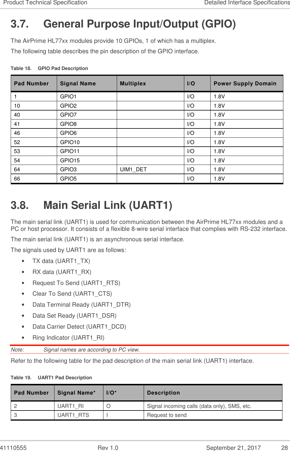
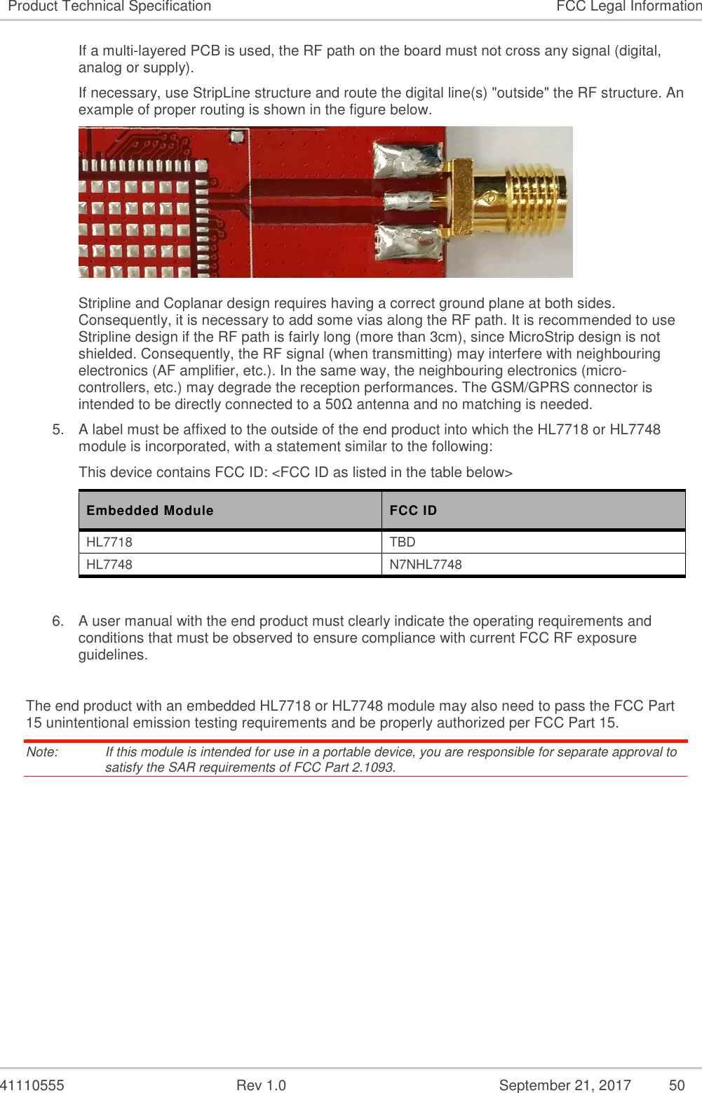
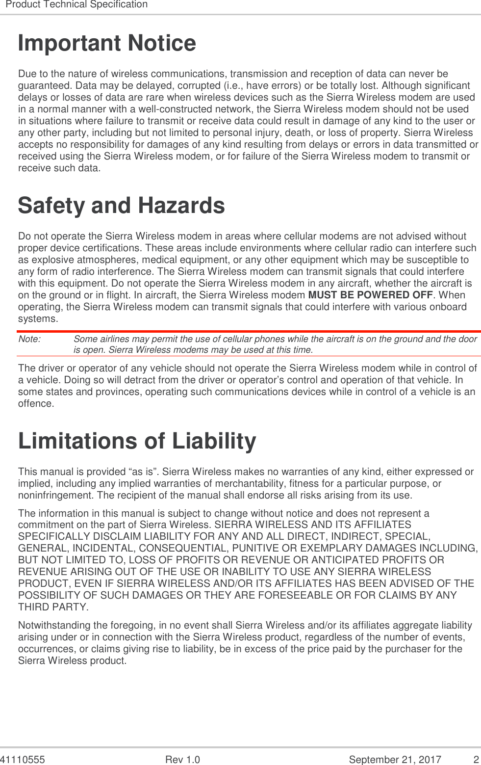
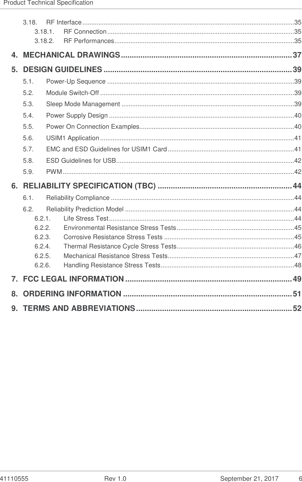
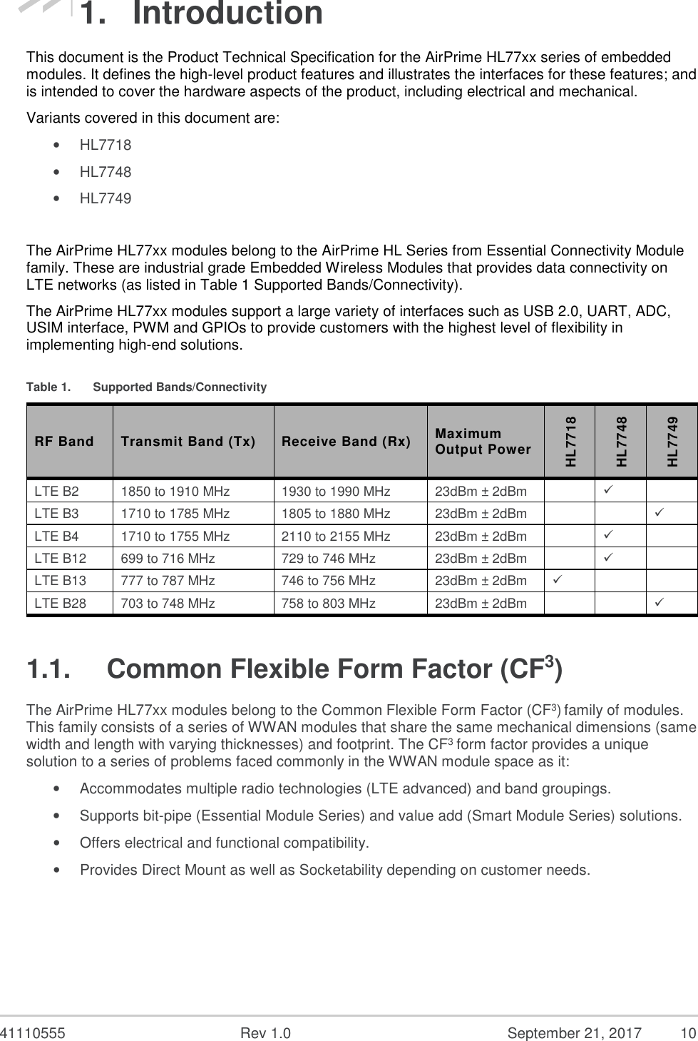
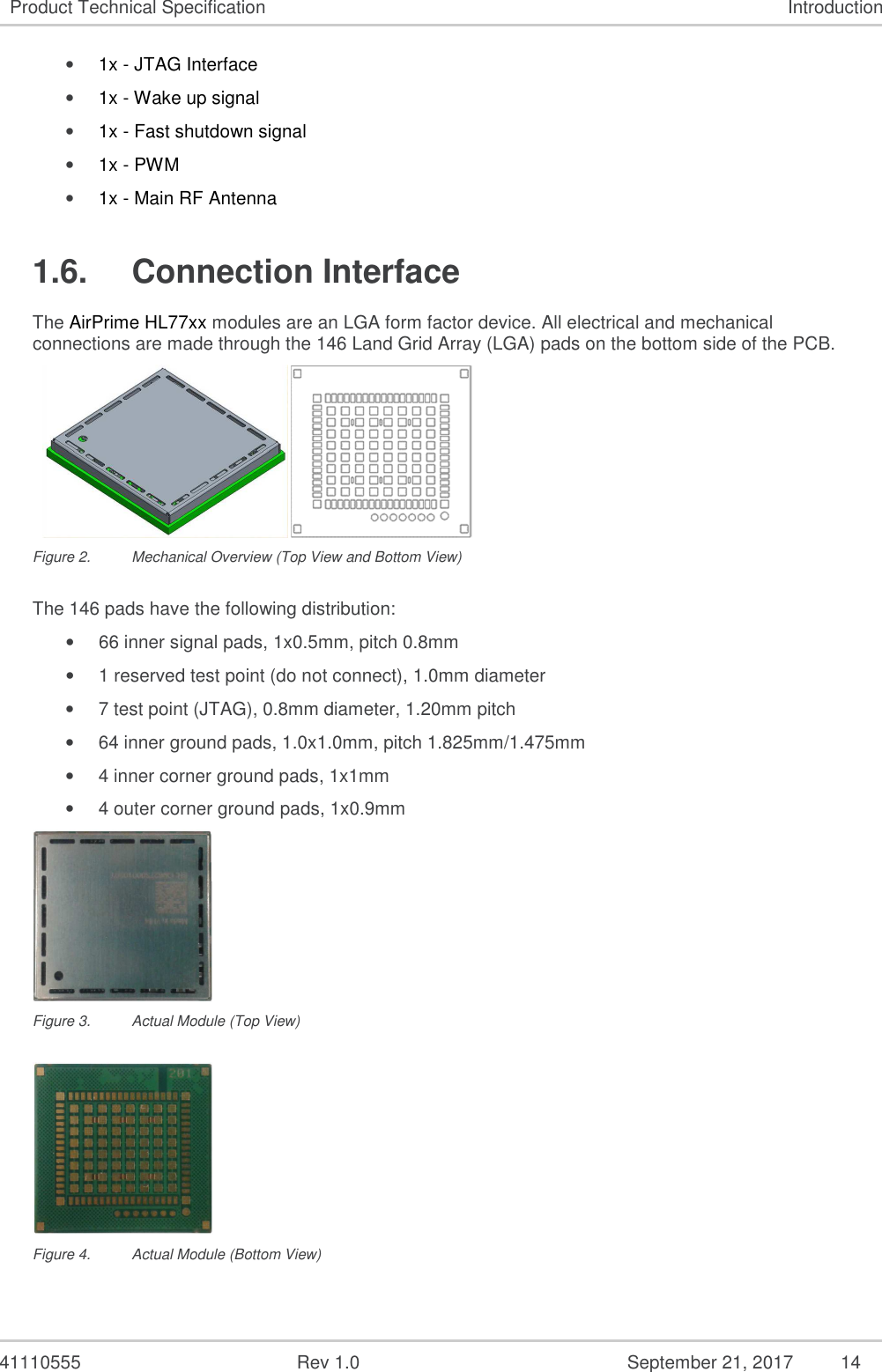
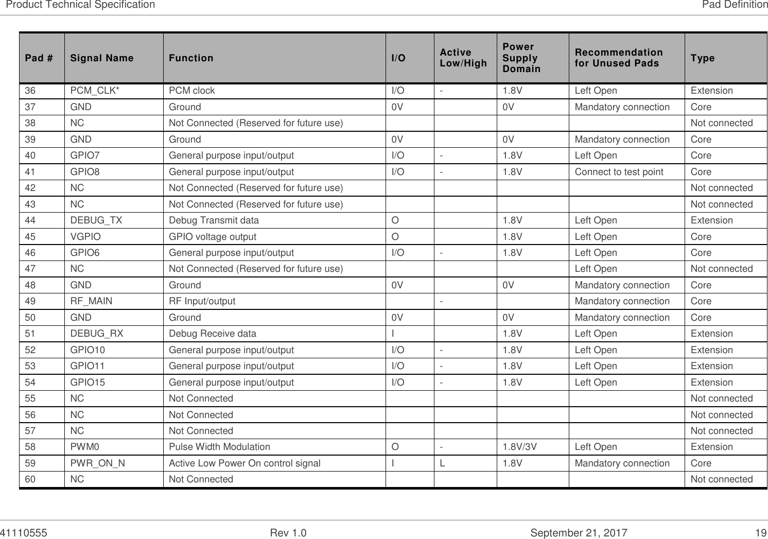
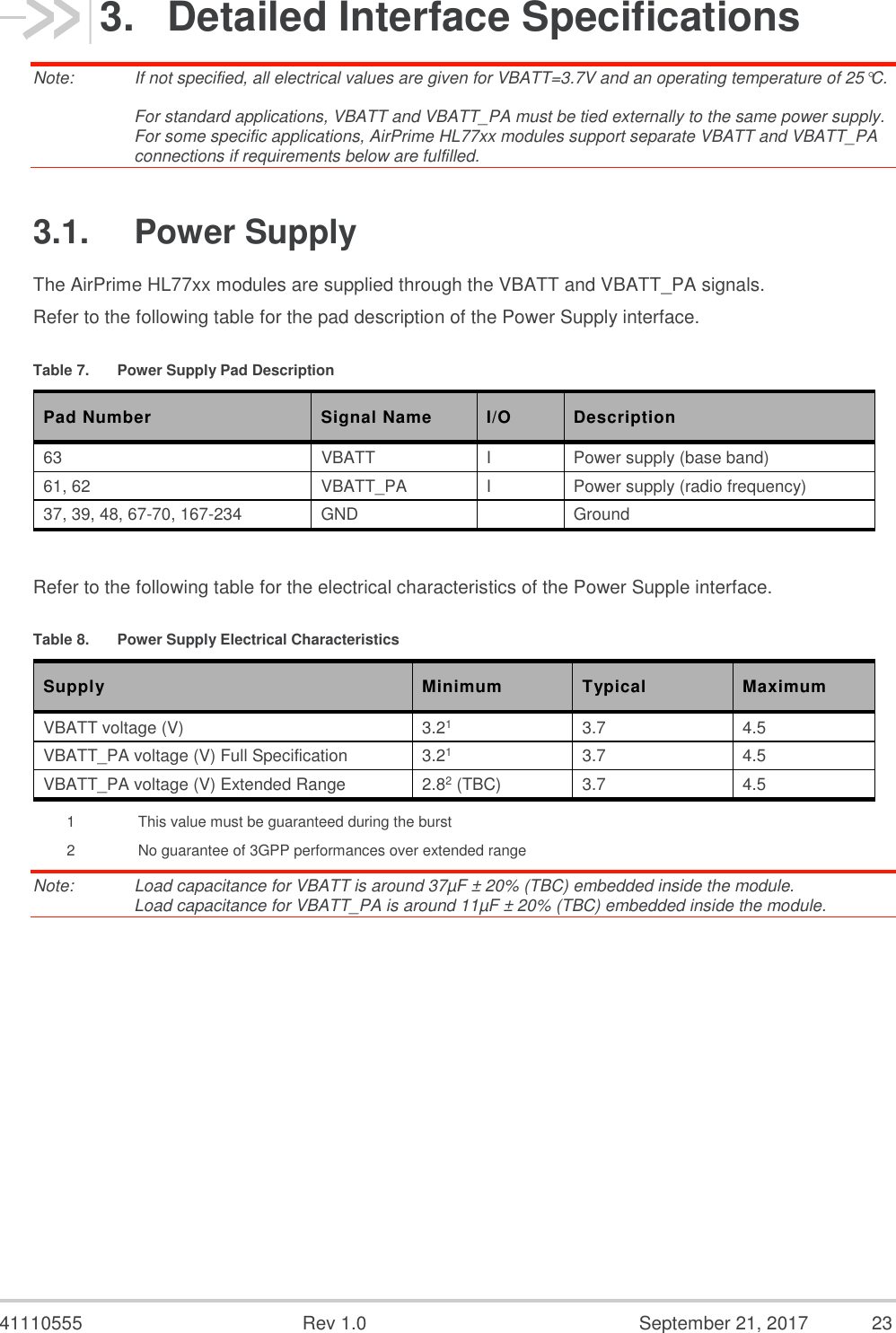
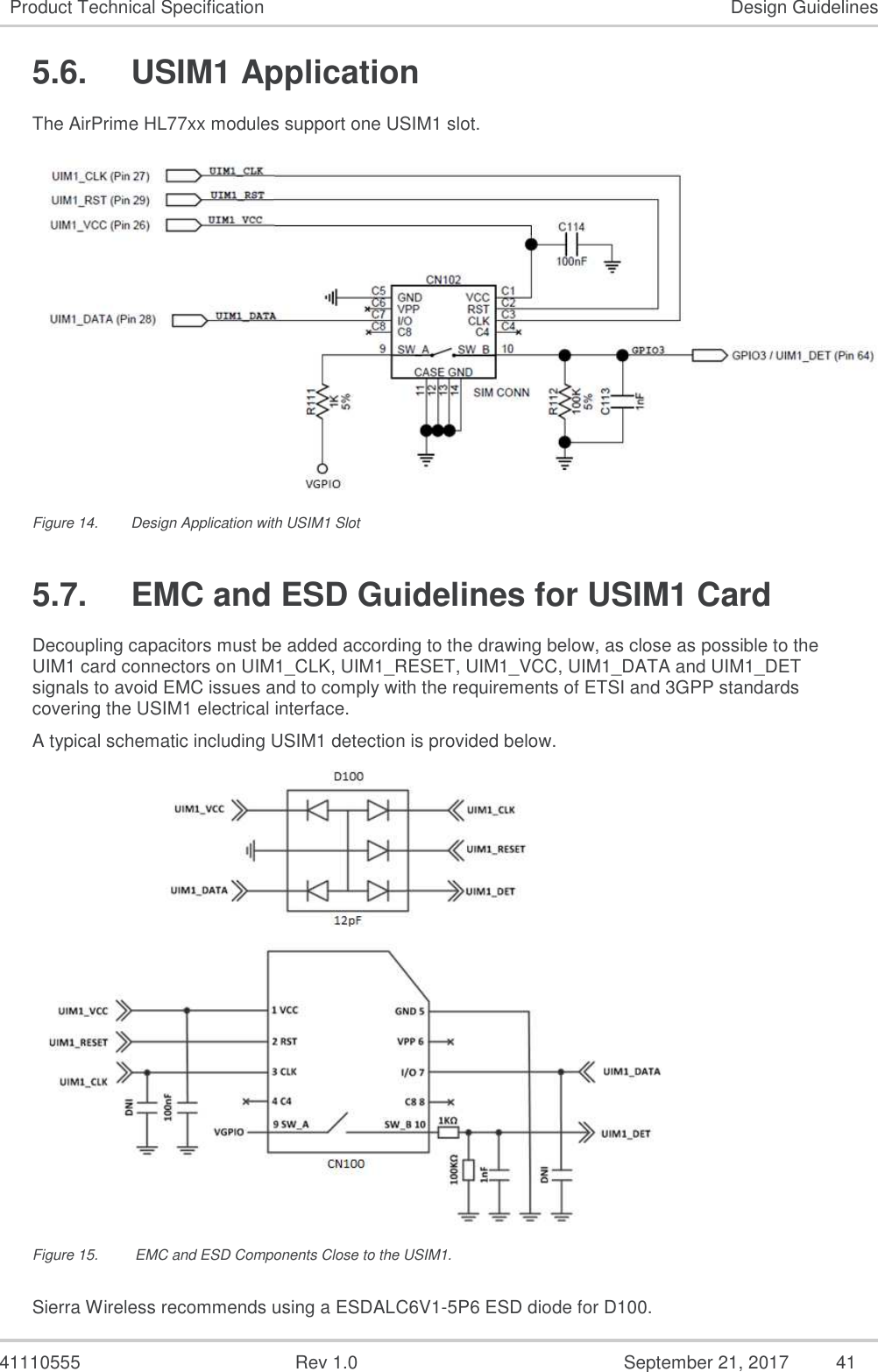
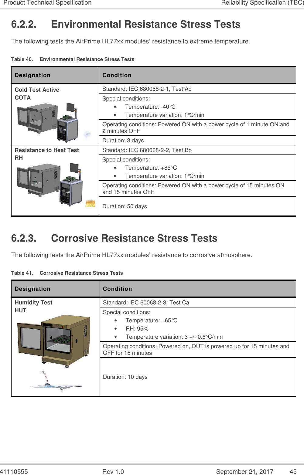
![41110555 Rev 1.0 September 21, 2017 32 Product Technical Specification Detailed Interface Specifications 3.12. Clock Interface The AirPrime HL77xx modules support two digital clock interfaces. Enabling or disabling the clock out feature can be done using AT commands. For more information about AT commands, refer to document [2] AirPrime HL77xx AT Commands Interface Guide. Refer to the following table for the pad description of the clock out interfaces. Table 26. Clock Interface Pad Description Pad Number Signal Name I/O I/O Type Description 22 GNSS_FREQ_OUT O 1.8V 26MHz Digital Clock output 23 32K_CLKOUT O 1.8V 32.768kHz Digital Clock output 3.13. Debug Interface The AirPrime HL77xx modules provide a 2-wire debug port interface. Table 27. Software Trace Pad Description Pad Number Signal Name* I/O* I/O Type Description 44 DEBUG_TX O 1.8V Debug Transmit Data 51 DEBUG_RX I 1.8V Debug Receive Data * According to module view. Note: It is strongly recommended to provide access through Test Points to this interface. 3.14. JTAG Interface The JTAG interface provides debug access to the core of the AirPrime HL77xx modules. These JTAG signals are accessible through solder-able test points. Refer to the following table for the pad description of the JTAG interface. Table 28. JTAG Pad Description Pad Number Signal Name Function 236 JTAG_RESET JTAG RESET 237 JTAG_TCK JTAG Test Clock 238 JTAG_TDO JTAG Test Data Output 239 JTAG_TMS JTAG Test Mode Select 240 JTAG_TRST JTAG Test Reset 241 JTAG_TDI JTAG Test Data Input Note: It is recommended to provide access through Test Points to this interface the JTAG pads (for Failure Analysis debugging). All signals listed in the table above should be outputs on the customer board to allow JTAG debugging.](https://usermanual.wiki/Sierra-Wireless/HL7748/User-Guide-3636301-Page-32.png)
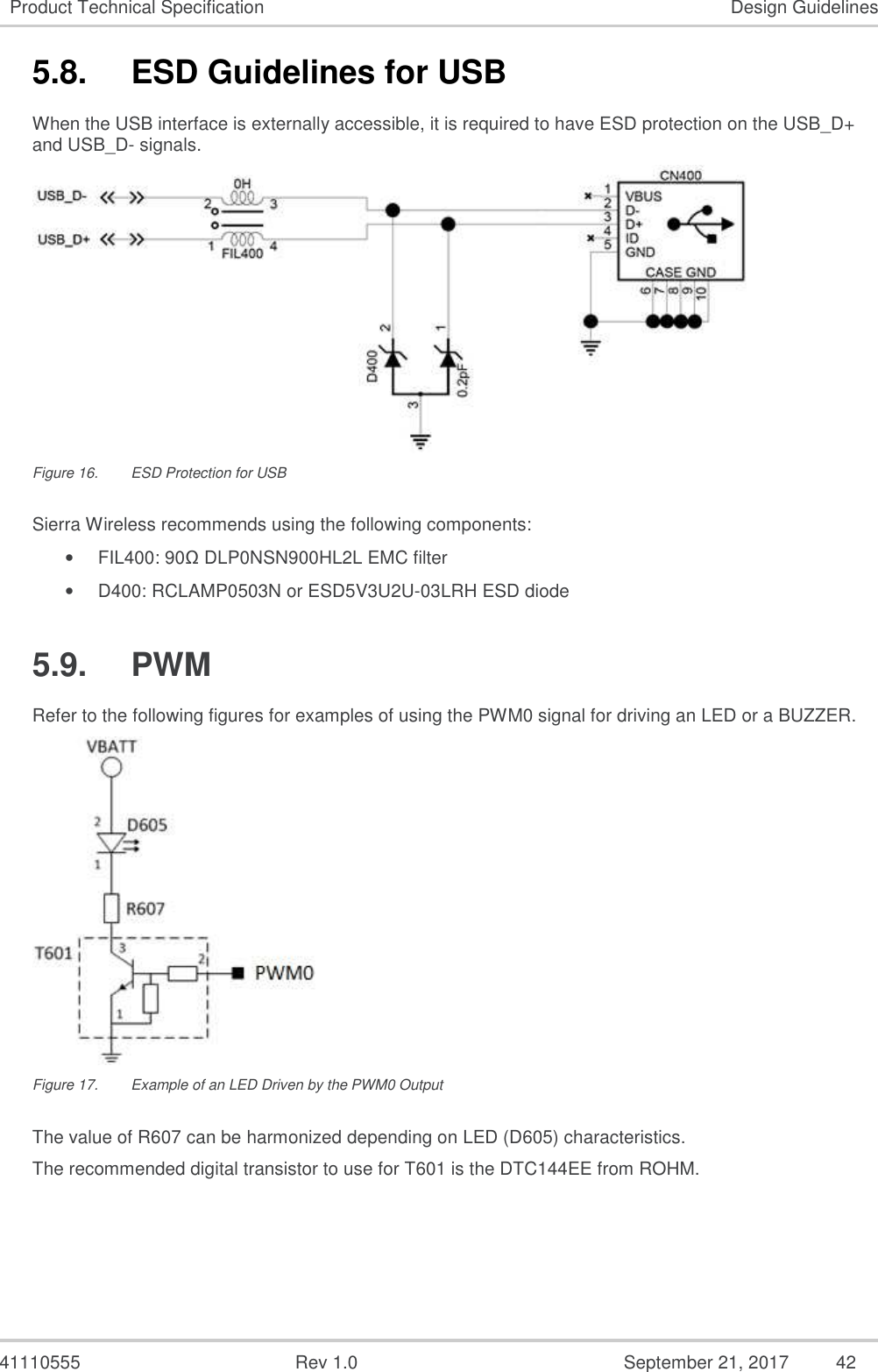
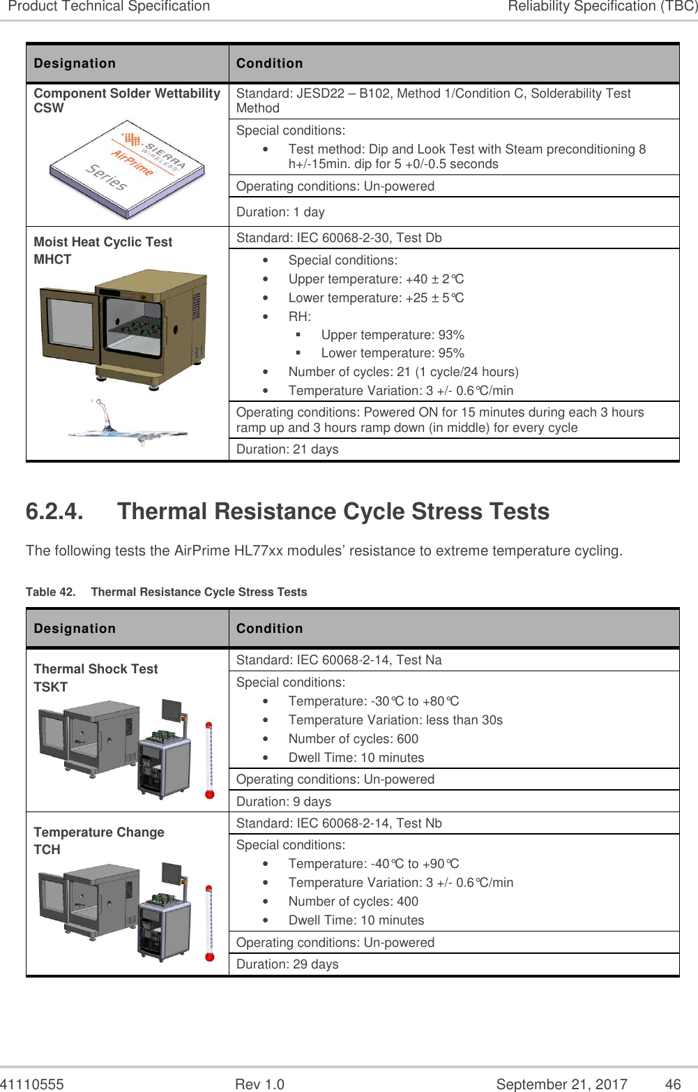
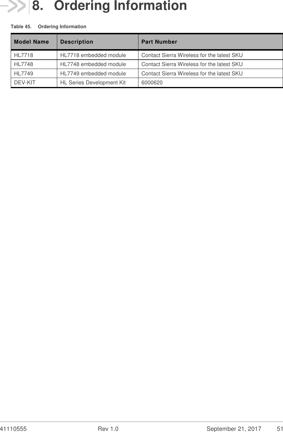
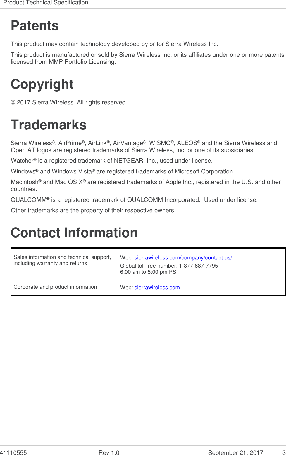
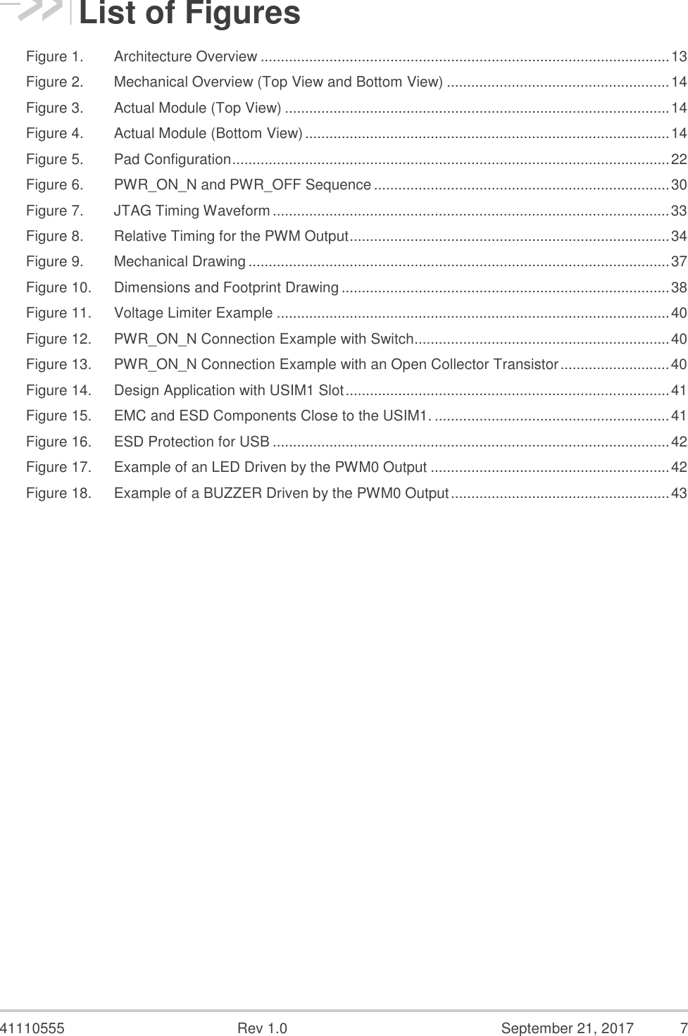
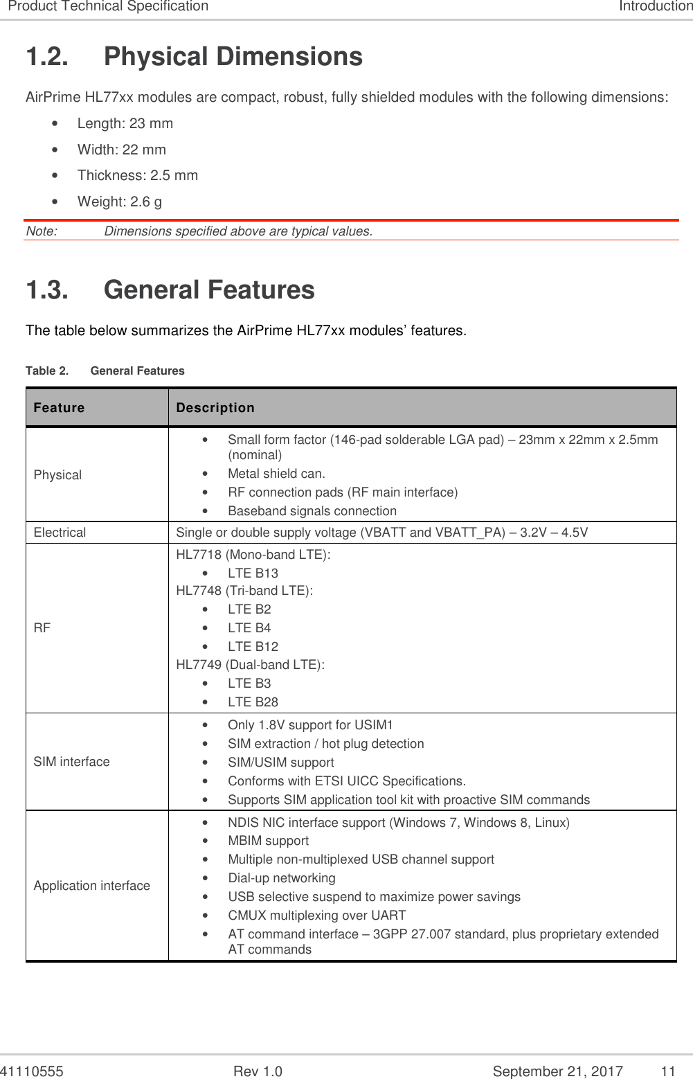
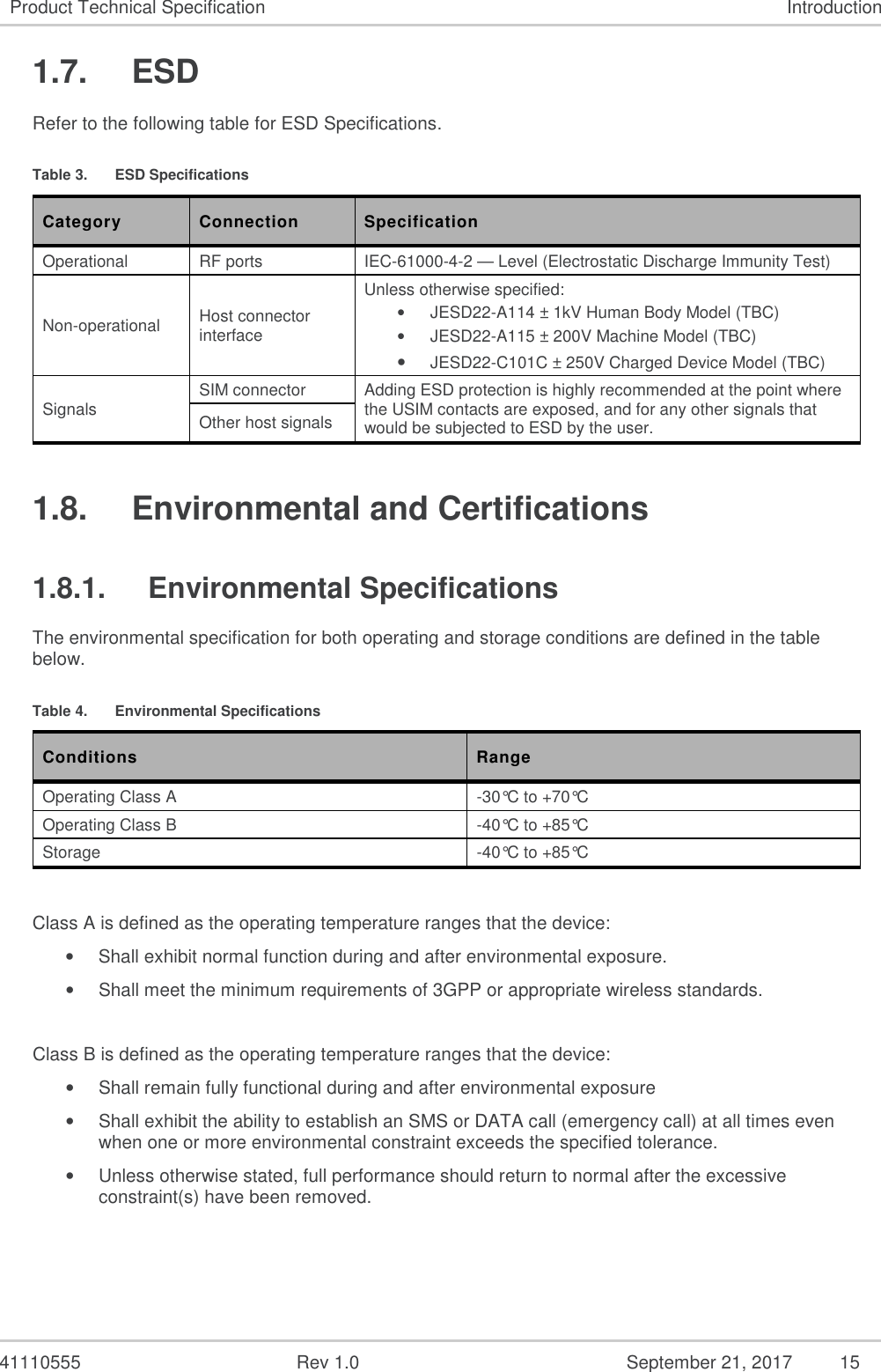
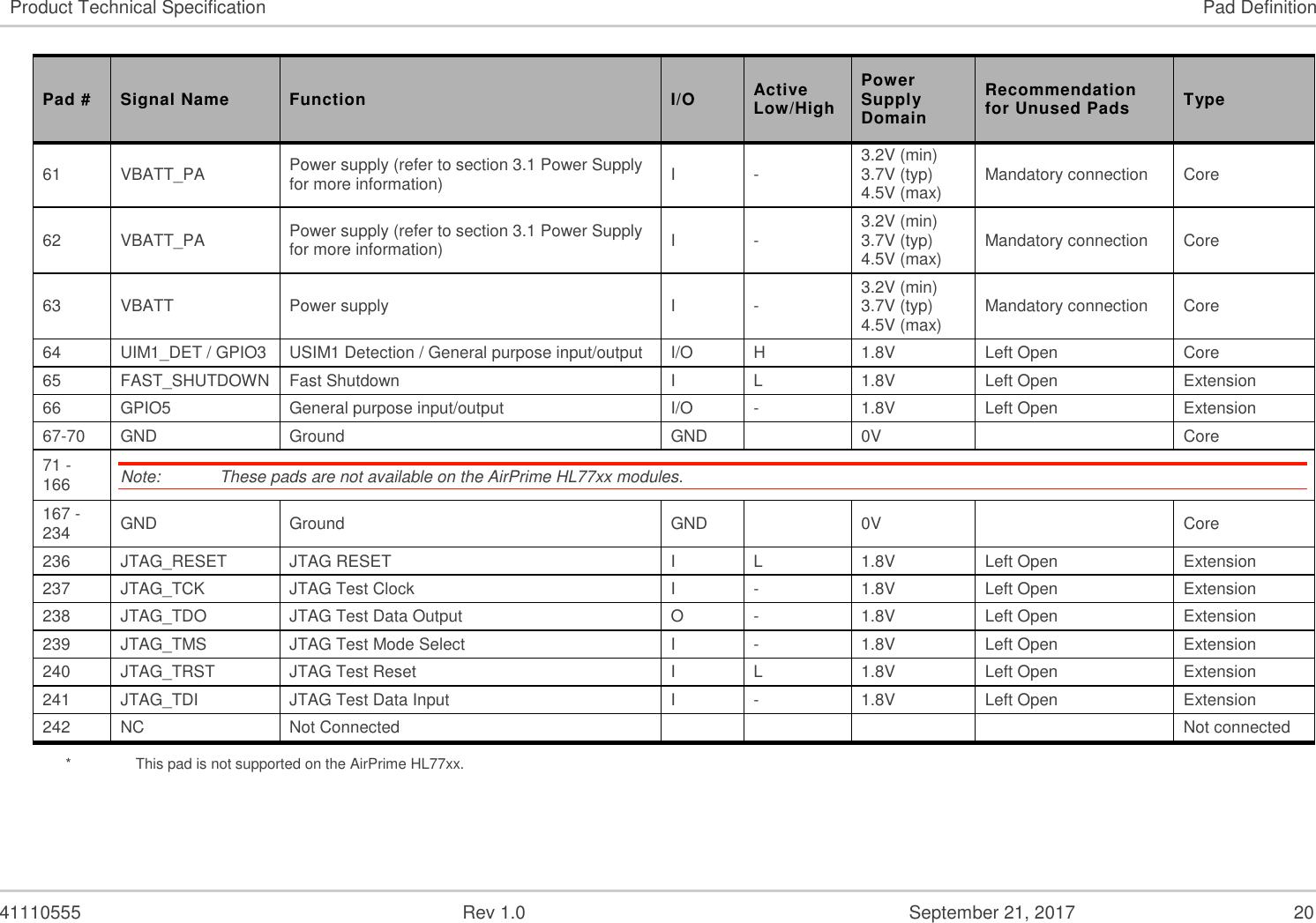
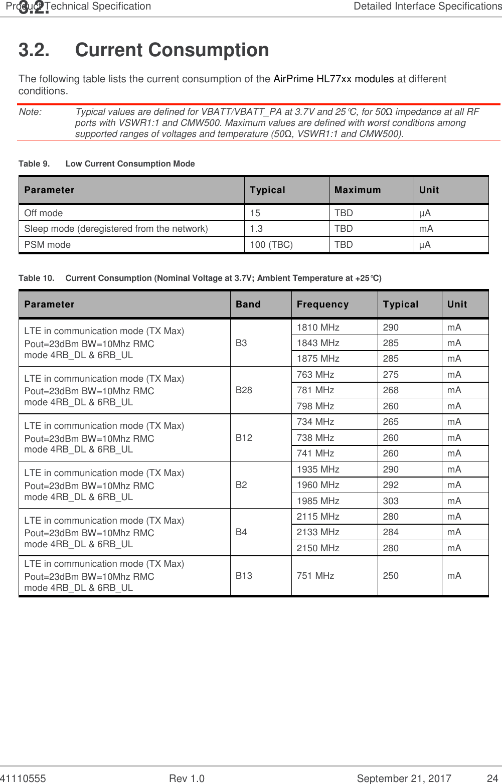
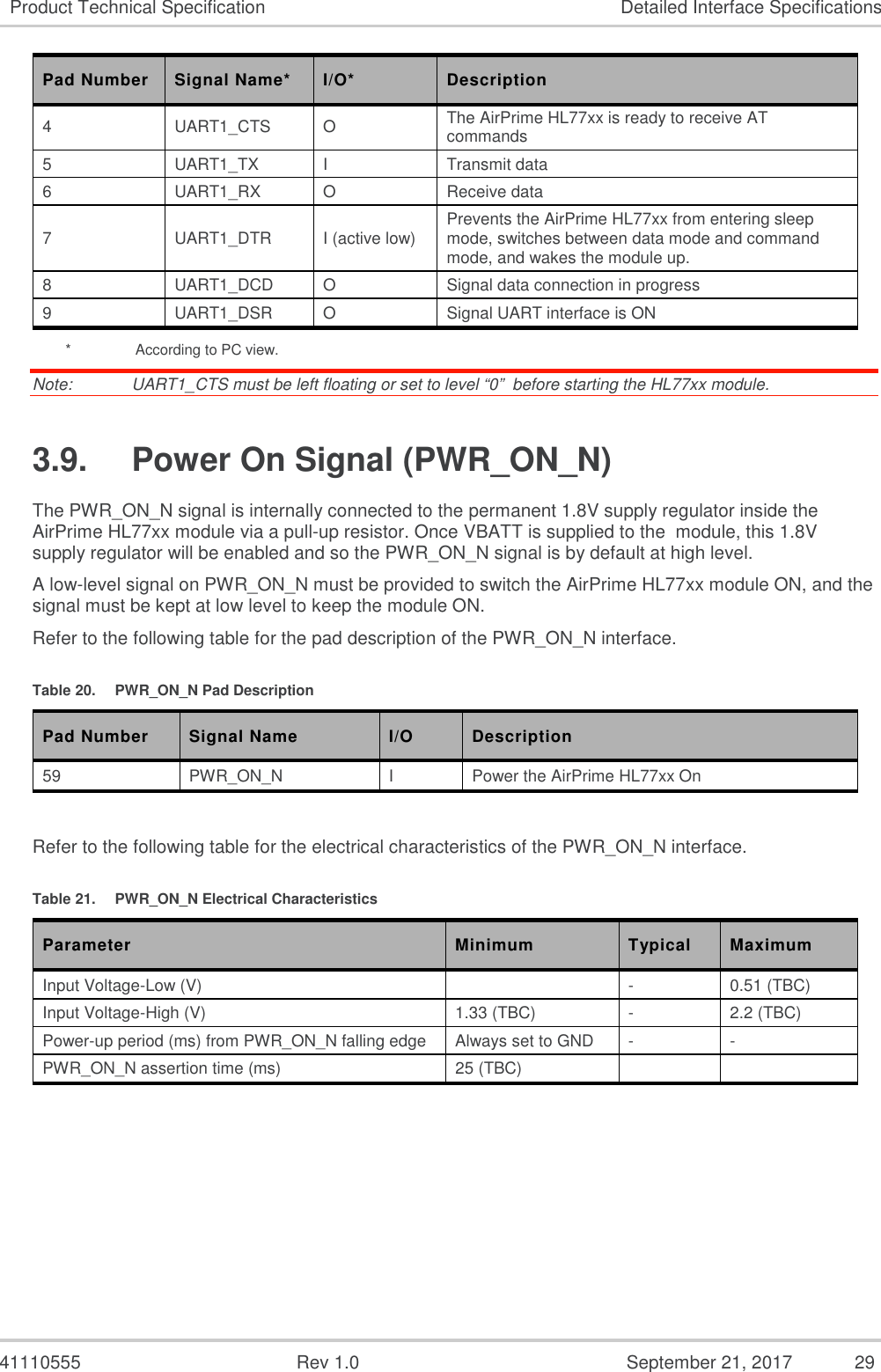
![41110555 Rev 1.0 September 21, 2017 47 Product Technical Specification Reliability Specification (TBC) 6.2.5. Mechanical Resistance Stress Tests The following tests the AirPrime HL77xx modules’ resistance to vibrations and mechanical shocks. Table 43. Mechanical Resistance Stress Tests Designation Condition Sinusoidal Vibration Test SVT Standard: IEC 60068-2-6, Test Fc Special conditions: • Frequency range: 16 Hz to 1000 Hz • Displacement: 0.35mm (peak-peak) • Acceleration: 5G from 16 to 62 Hz 3G from 62 to 200 Hz 1G from 200 to 1000 Hz • Sweep rate: 1 octave / cycle • Number of Sweep: 20 sweeps/axis • Sweep direction: ±X, ±Y, ±Z Operating conditions: Un-powered Duration: 2 days Random Vibration Test RVT Standard: IEC 60068-2-64, Test Fh Special conditions: • Frequency range: 10 Hz – 2000 Hz • Power Spectral Density in [(m/s²)²/Hz] g2/Hz at 10Hz g2/Hz at 250Hz 0.005 g2/Hz at 1000Hz 0.005 g2/Hz at 2000Hz • Peak factor: 3 • Duration per Axis: 1 hr / axis Operating conditions: Un-powered Duration: 1 day Mechanical Shock Test MST Standard: IEC 60068-2-27, Test Ea Special conditions: • Shock Test 1: Wave form: Half sine Peak acceleration: 30g Duration: 11ms Number of shocks: 8 Direction: ±X, ±Y, ±Z • Shock Test 2: Wave form: Half sine Peak acceleration: 100g Duration: 6ms Number of shocks: 3 Direction: ±X, ±Y, ±Z Operating conditions: Un-powered Duration: 72 hours](https://usermanual.wiki/Sierra-Wireless/HL7748/User-Guide-3636301-Page-47.png)