Sierra Wireless HL8528 Embedded module User Manual
Sierra Wireless Inc. Embedded module
UserManual.wiki
>
Sierra Wireless
>
HL8528 User Manual
User manual
Navigation menu
Upload a User Manual
Namespaces
Wiki Guide
HTML
PDF
Info
Views
User Manual
Discussion / Help
Navigation
![4117047 Rev 2.2 December 18, 2015 16 Product Technical Specification Introduction 1.9.2. Regulatory The AirPrime HL8518, HL8528 and HL8529 modules are compliant with the following regulations: R&TTE directive 1999/5/EC FCC IC These compliances will be reflected on the AirPrime HL8518, HL8528 and HL8529 modules labels when applicable. 1.9.3. RoHS Directive Compliant The AirPrime HL8518, HL8528 and HL8529 modules are compliant with RoHS Directive 2011/65/EU which sets limits for the use of certain restricted hazardous substances. This directive states that “from 1st July 2006, new electrical and electronic equipment put on the market does not contain lead, mercury, cadmium, hexavalent chromium, polybrominated biphenyls (PBB) or polybrominated diphenyl ethers (PBDE)”. 1.9.4. Disposing of the Product This electronic product is subject to the EU Directive 2012/19/EU for Waste Electrical and Electronic Equipment (WEEE). As such, this product must not be disposed of at a municipal waste collection point. Please refer to local regulations for directions on how to dispose of this product in an environmental friendly manner. 1.10. References [1] AirPrime HL Series Customer Process Guidelines Reference Number: 4114330 [2] AirPrime HL6 and HL8 Series AT Commands Interface Guide Reference Number: 4114680 [3] AirPrime HL Series Dual SIM Single Standby Application Note Reference Number: 2174034](https://usermanual.wiki/Sierra-Wireless/HL8528/User-Guide-2871500-Page-16.png)
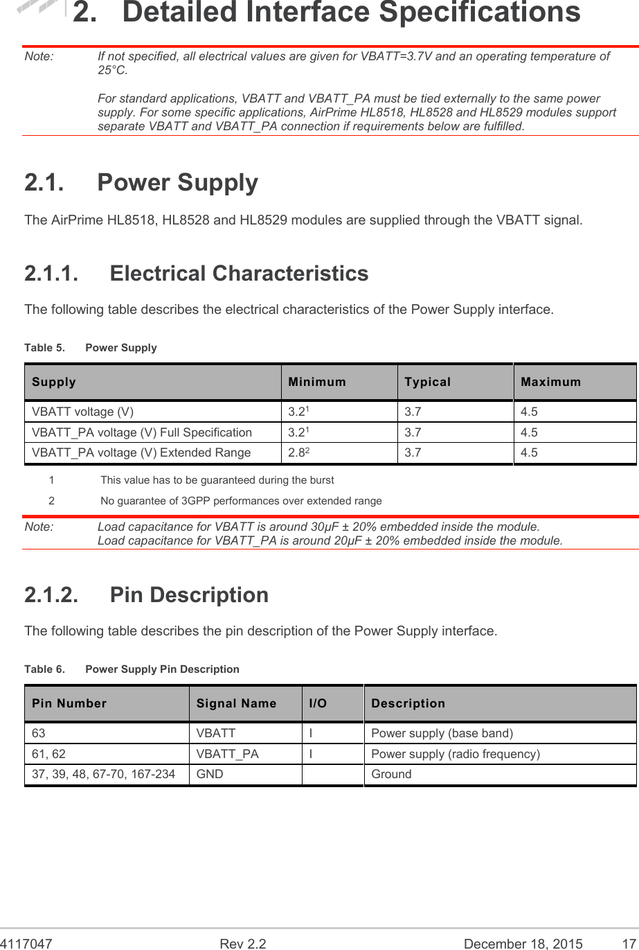
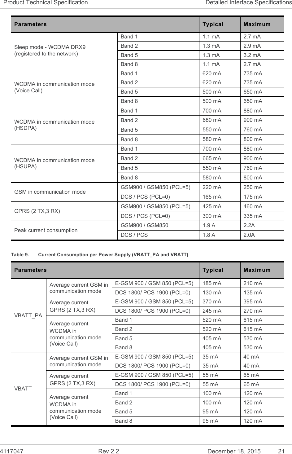
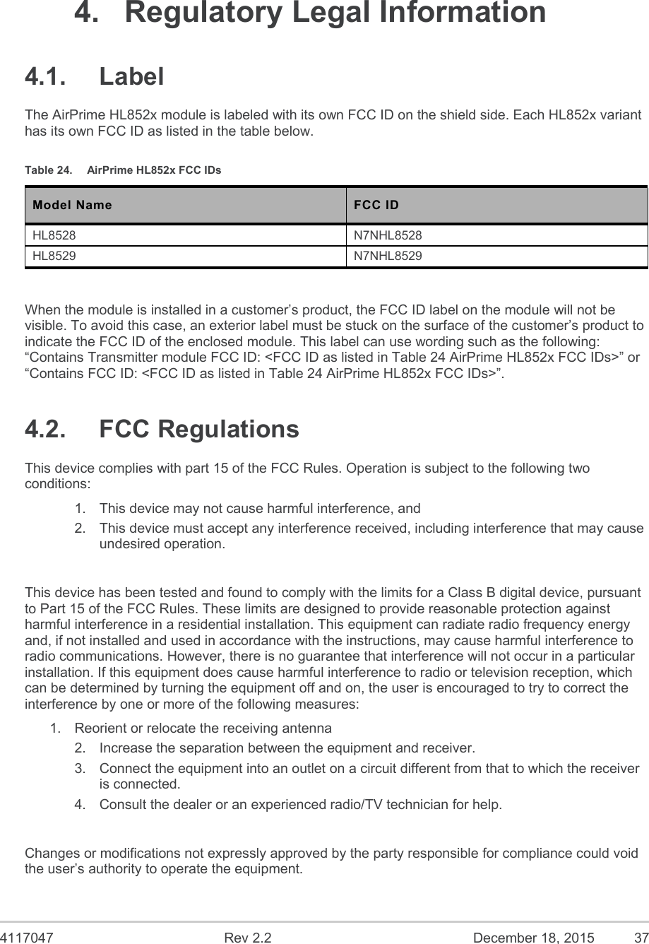
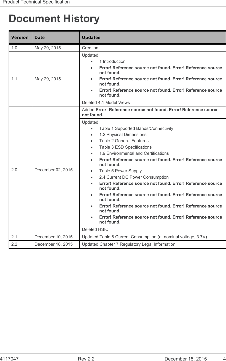
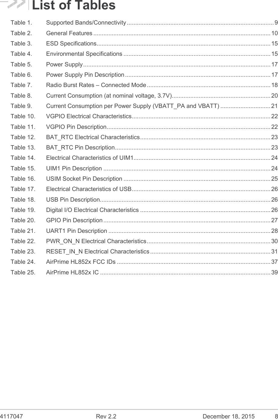
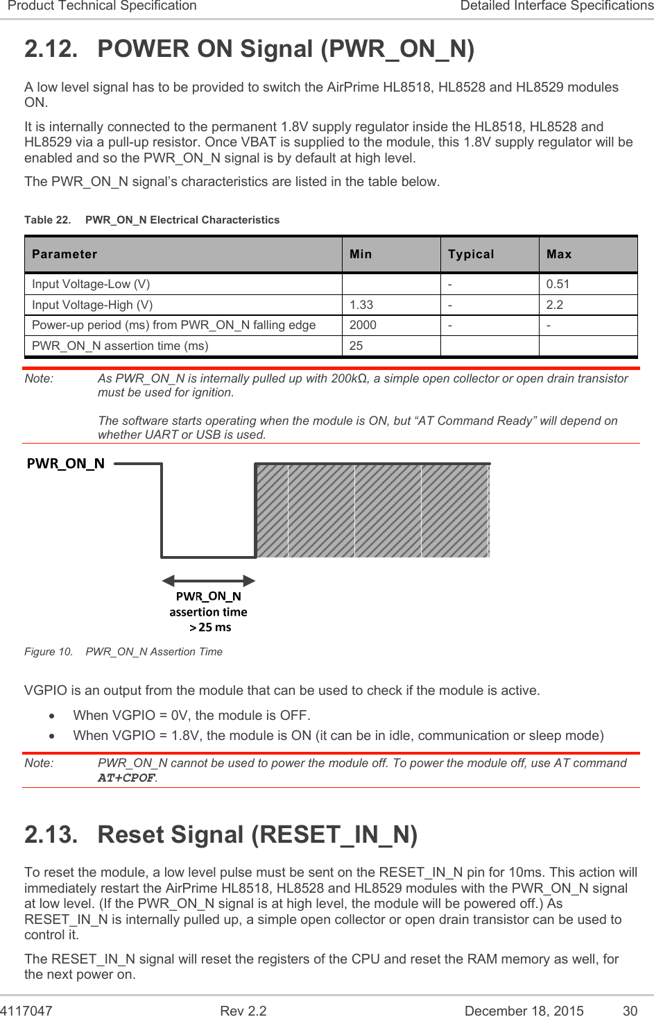
![4117047 Rev 2.2 December 18, 2015 25 Product Technical Specification Detailed Interface Specifications 2.7.3. UIM1_DET UIM1_DET is used to detect and notify the application about the insertion and removal of a SIM device in the SIM socket connected to the main SIM interface (UIM1). When a SIM is inserted, the state of UIM1_DET transitions from logic 0 to logic 1. Inversely, when a SIM is removed, the state of UIM1_DET transitions from logic 1 to logic 0. The GPIO used for UIM1_DET is GPIO3. Enabling or disabling this SIM detect feature can be done using the AT+KSIMDET command. For more information about this command, refer to document [2] AirPrime HL6 and HL8 Series AT Commands Interface Guide. 2.7.4. Application 2.7.4.1. Reference Schematic Figure 6. UIM1 Application Reference Schematic 2.7.4.2. USIM Socket Pin Description The following table describes the required USIM socket pins. Table 16. USIM Socket Pin Description Pin Number Signal Name Description 1 UIM1_VCC UIM1 Power supply 2 UIM1_RESET UIM1 Reset 3 UIM1_CLK UIM1 Clock 4 UIM1_DET UIM1 detection 5 GROUND GND 6 - - 7 UIM1_DATA UIM1 Data 8 VGPIO Power supply](https://usermanual.wiki/Sierra-Wireless/HL8528/User-Guide-2871500-Page-25.png)
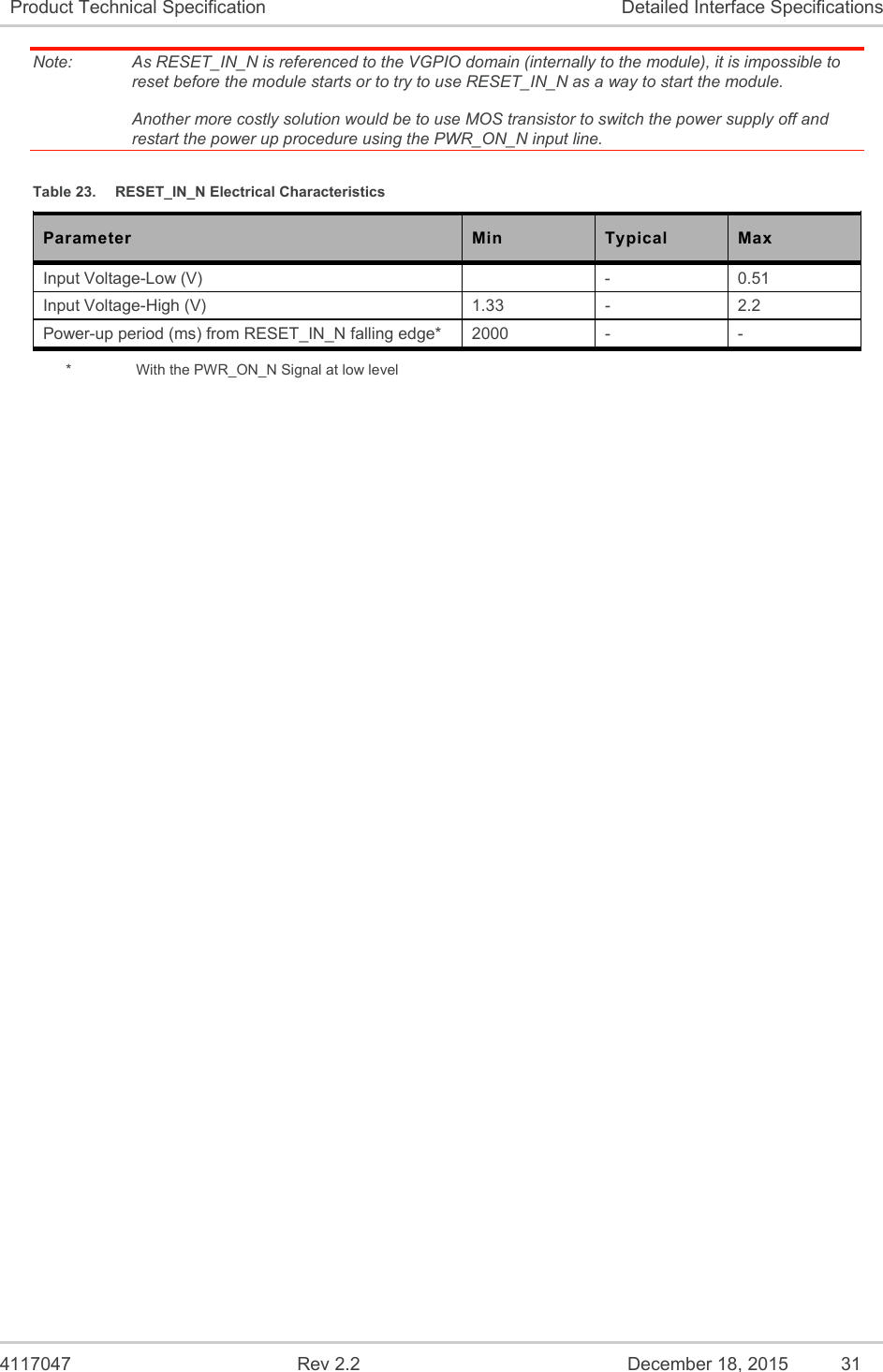
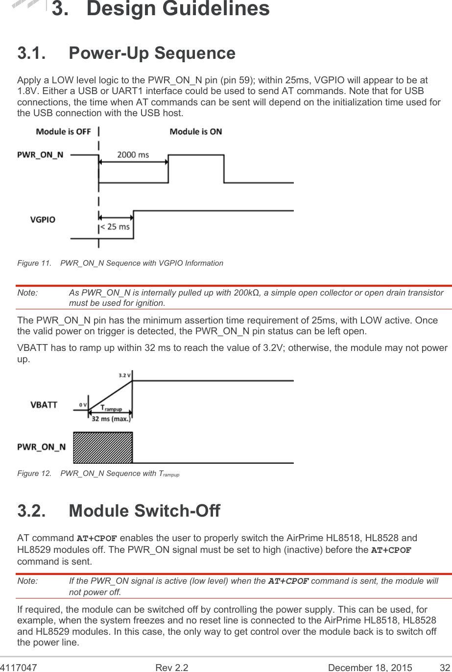
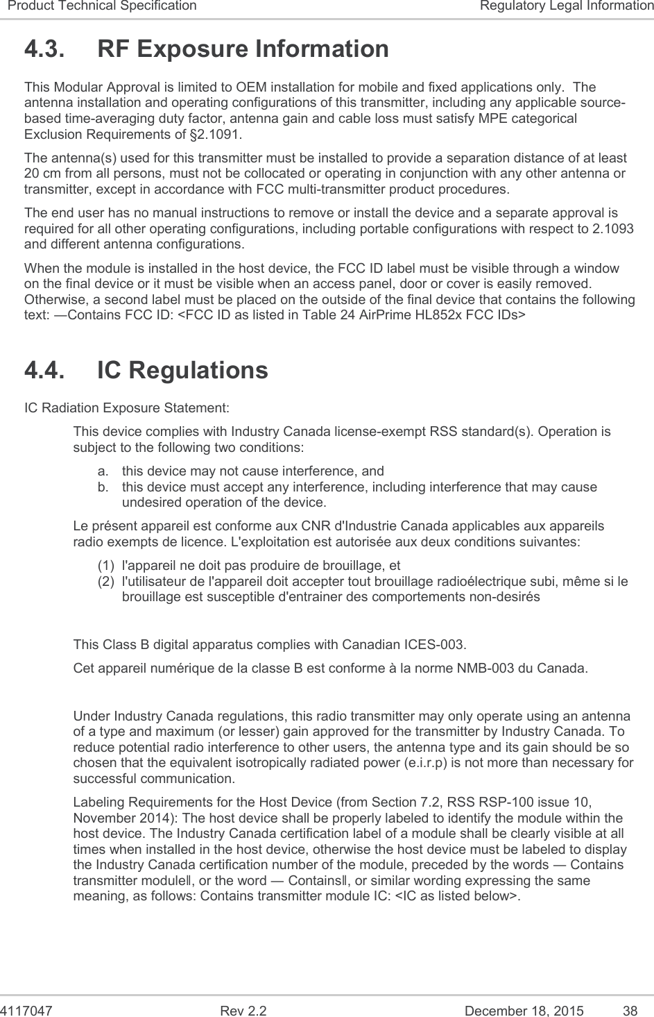
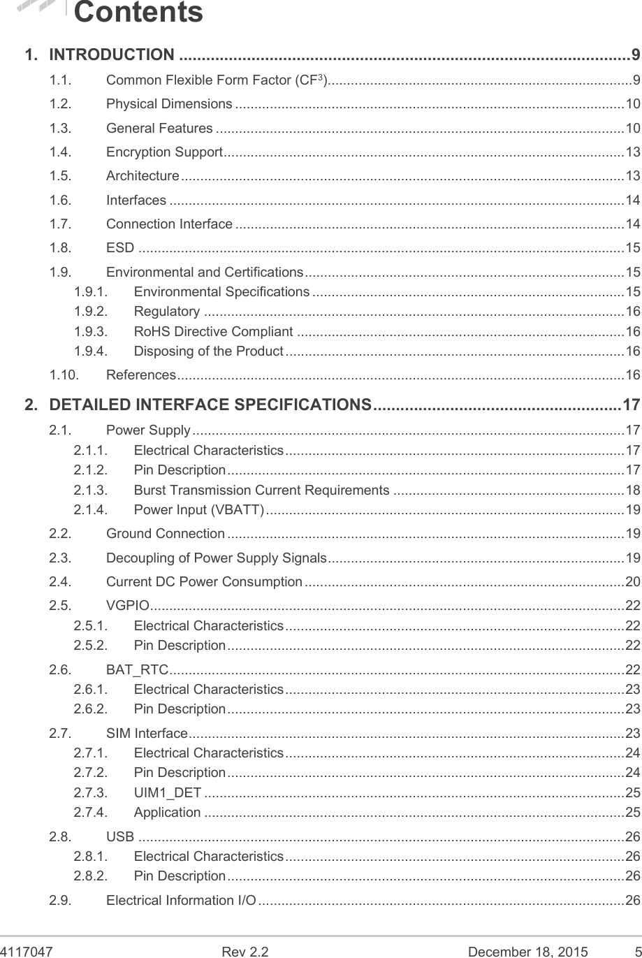
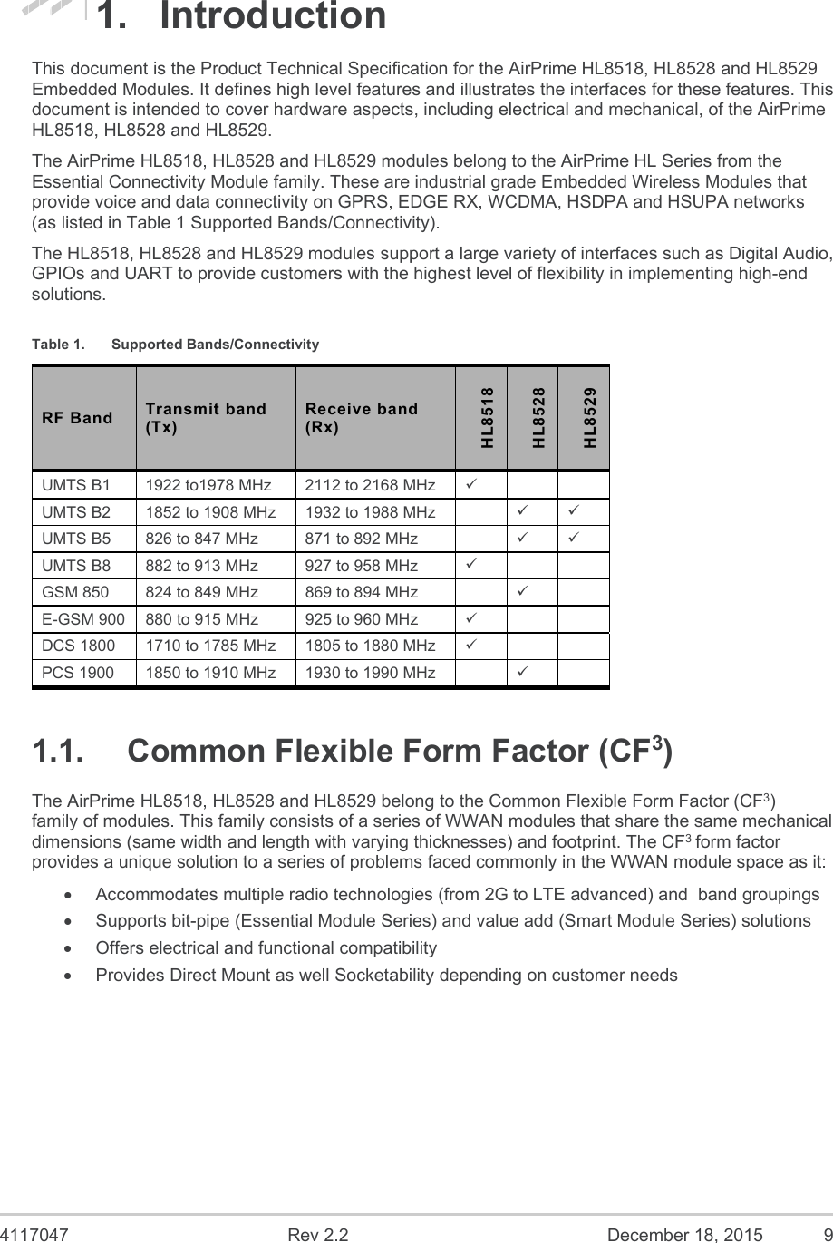
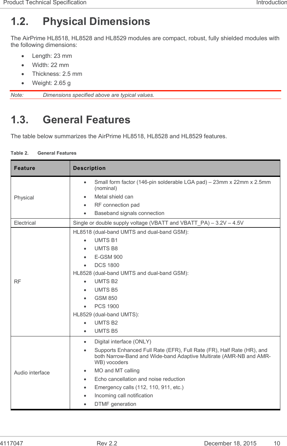
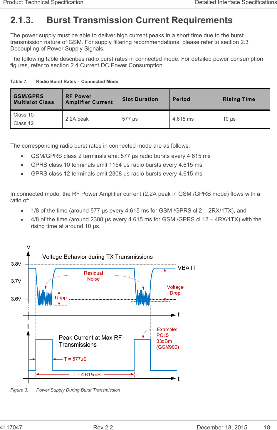
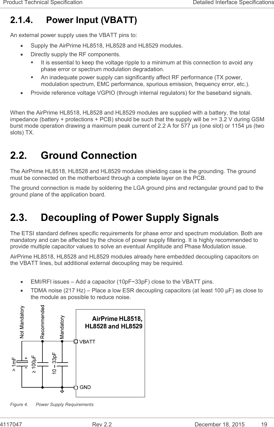
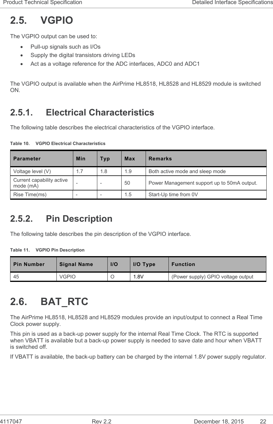
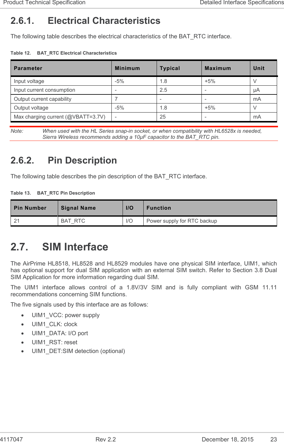
![4117047 Rev 2.2 December 18, 2015 35 Product Technical Specification Design Guidelines 3.7. ESD Guidelines for USB When the USB interface is externally accessible, it is required to have ESD protection on the USB_VBUS, USB_D+ and USB_D- signals. Figure 16. ESD Protection for USB Note: It is not recommended to have an ESD diode with feedback path from USB_VBUS to either USB_D+ or USB_D-. 3.8. Dual SIM Application Using an external switch and GPIOs, the AirPrime HL8518, HL8528 and HL8529 modules can support Dual SIM Single Standby with fast network switching. Refer to document [2] AirPrime HL6 and HL8 Series AT Commands Interface Guide for related AT commands. Figure 17. Reference Design for Dual SIM Application](https://usermanual.wiki/Sierra-Wireless/HL8528/User-Guide-2871500-Page-35.png)