Sierra Wireless HL8529 Embedded module User Manual
Sierra Wireless Inc. Embedded module
User manual

AirPrime HL8518, HL8528 and HL8529
4117047
2.2
December 18, 2015
Product Technical Specification

4117047 Rev 2.2 December 18, 2015 2
Product Technical Specification
Important Notice
Due to the nature of wireless communications, transmission and reception of data can never be
guaranteed. Data may be delayed, corrupted (i.e., have errors) or be totally lost. Although significant
delays or losses of data are rare when wireless devices such as the Sierra Wireless modem are used
in a normal manner with a well-constructed network, the Sierra Wireless modem should not be used
in situations where failure to transmit or receive data could result in damage of any kind to the user or
any other party, including but not limited to personal injury, death, or loss of property. Sierra Wireless
accepts no responsibility for damages of any kind resulting from delays or errors in data transmitted or
received using the Sierra Wireless modem, or for failure of the Sierra Wireless modem to transmit or
receive such data.
Safety and Hazards
Do not operate the Sierra Wireless modem in areas where cellular modems are not advised without
proper device certifications. These areas include environments where cellular radio can interfere such
as explosive atmospheres, medical equipment, or any other equipment which may be susceptible to
any form of radio interference. The Sierra Wireless modem can transmit signals that could interfere
with this equipment. Do not operate the Sierra Wireless modem in any aircraft, whether the aircraft is
on the ground or in flight. In aircraft, the Sierra Wireless modem MUST BE POWERED OFF. When
operating, the Sierra Wireless modem can transmit signals that could interfere with various onboard
systems.
Note: Some airlines may permit the use of cellular phones while the aircraft is on the ground and the door
is open. Sierra Wireless modems may be used at this time.
The driver or operator of any vehicle should not operate the Sierra Wireless modem while in control of
a vehicle. Doing so will detract from the driver or operator’s control and operation of that vehicle. In
some states and provinces, operating such communications devices while in control of a vehicle is an
offence.
Limitations of Liability
This manual is provided “as is”. Sierra Wireless makes no warranties of any kind, either expressed or
implied, including any implied warranties of merchantability, fitness for a particular purpose, or
noninfringement. The recipient of the manual shall endorse all risks arising from its use.
The information in this manual is subject to change without notice and does not represent a
commitment on the part of Sierra Wireless. SIERRA WIRELESS AND ITS AFFILIATES
SPECIFICALLY DISCLAIM LIABILITY FOR ANY AND ALL DIRECT, INDIRECT, SPECIAL,
GENERAL, INCIDENTAL, CONSEQUENTIAL, PUNITIVE OR EXEMPLARY DAMAGES INCLUDING,
BUT NOT LIMITED TO, LOSS OF PROFITS OR REVENUE OR ANTICIPATED PROFITS OR
REVENUE ARISING OUT OF THE USE OR INABILITY TO USE ANY SIERRA WIRELESS
PRODUCT, EVEN IF SIERRA WIRELESS AND/OR ITS AFFILIATES HAS BEEN ADVISED OF THE
POSSIBILITY OF SUCH DAMAGES OR THEY ARE FORESEEABLE OR FOR CLAIMS BY ANY
THIRD PARTY.
Notwithstanding the foregoing, in no event shall Sierra Wireless and/or its affiliates aggregate liability
arising under or in connection with the Sierra Wireless product, regardless of the number of events,
occurrences, or claims giving rise to liability, be in excess of the price paid by the purchaser for the
Sierra Wireless product.
Customer understands that Sierra Wireless is not providing cellular or GPS (including A-GPS)
services. These services are provided by a third party and should be purchased directly by the
Customer.

4117047 Rev 2.2 December 18, 2015 3
Product Technical Specification
SPECIFIC DISCLAIMERS OF LIABILITY: CUSTOMER RECOGNIZES AND ACKNOWLEDGES
SIERRA WIRELESS IS NOT RESPONSIBLE FOR AND SHALL NOT BE HELD LIABLE FOR ANY
DEFECT OR DEFICIENCY OF ANY KIND OF CELLULAR OR GPS (INCLUDING A-GPS)
SERVICES.
Patents
This product may contain technology developed by or for Sierra Wireless Inc.
This product includes technology licensed from QUALCOMM®.
This product is manufactured or sold by Sierra Wireless Inc. or its affiliates under one or more patents
licensed from InterDigital Group and MMP Portfolio Licensing.
Copyright
© 2015 Sierra Wireless. All rights reserved.
Trademarks
Sierra Wireless®, AirPrime®, AirLink®, AirVantage®, WISMO®, ALEOS® and the Sierra Wireless and
Open AT logos are registered trademarks of Sierra Wireless, Inc. or one of its subsidiaries.
Watcher® is a registered trademark of NETGEAR, Inc., used under license.
Windows® and Windows Vista® are registered trademarks of Microsoft Corporation.
Macintosh® and Mac OS X® are registered trademarks of Apple Inc., registered in the U.S. and other
countries.
QUALCOMM® is a registered trademark of QUALCOMM Incorporated. Used under license.
Other trademarks are the property of their respective owners.
Contact Information
Sales Desk:
Phone: 1-604-232-1488
Hours: 8:00 AM to 5:00 PM Pacific Time
Contact: http://www.sierrawireless.com/sales
Post:
Sierra Wireless
13811 Wireless Way
Richmond, BC
Canada V6V 3A4
Technical Support: support@sierrawireless.com
RMA Support: repairs@sierrawireless.com
Fax: 1-604-231-1109
Web: http://www.sierrawireless.com/
Consult our website for up-to-date product descriptions, documentation, application notes, firmware
upgrades, troubleshooting tips, and press releases: www.sierrawireless.com
4117047 Rev 2.2 December 18, 2015 4
Product Technical Specification
Document History
Version Date Updates
1.0 May 20, 2015 Creation
1.1 May 29, 2015
Updated:
1 Introduction
Error! Reference source not found. Error! Reference source
not found.
Error! Reference source not found. Error! Reference source
not found.
Error! Reference source not found. Error! Reference source
not found.
Deleted 4.1 Model Views
2.0 December 02, 2015
Added Error! Reference source not found. Error! Reference source
not found.
Updated:
Table 1 Supported Bands/Connectivity
1.2 Physical Dimensions
Table 2 General Features
Table 3 ESD Specifications
1.9 Environmental and Certifications
Error! Reference source not found. Error! Reference source
not found.
Table 5 Power Supply
2.4 Current DC Power Consumption
Error! Reference source not found. Error! Reference source
not found.
Error! Reference source not found. Error! Reference source
not found.
Error! Reference source not found. Error! Reference source
not found.
Error! Reference source not found. Error! Reference source Error! Reference source not found. Error! Reference source
not found.
Deleted HSIC
2.1 December 10, 2015 Updated Table 8 Current Consumption (at nominal voltage, 3.7V)
2.2 December 18, 2015 Updated Chapter 7 Regulatory Legal Information

4117047 Rev 2.2 December 18, 2015 5
Contents
1.INTRODUCTION .................................................................................................... 9
1.1.Common Flexible Form Factor (CF3) ............................................................................... 9
1.2.Physical Dimensions ..................................................................................................... 10
1.3.General Features .......................................................................................................... 10
1.4.Encryption Support ........................................................................................................ 13
1.5.Architecture ................................................................................................................... 13
1.6.Interfaces ...................................................................................................................... 14
1.7.Connection Interface ..................................................................................................... 14
1.8.ESD .............................................................................................................................. 15
1.9.Environmental and Certifications ................................................................................... 15
1.9.1.Environmental Specifications ................................................................................. 15
1.9.2.Regulatory ............................................................................................................. 16
1.9.3.RoHS Directive Compliant ..................................................................................... 16
1.9.4.Disposing of the Product ........................................................................................ 16
1.10.References .................................................................................................................... 16
2.DETAILED INTERFACE SPECIFICATIONS ....................................................... 17
2.1.Power Supply ................................................................................................................ 17
2.1.1.Electrical Characteristics ........................................................................................ 17
2.1.2.Pin Description ....................................................................................................... 17
2.1.3.Burst Transmission Current Requirements ............................................................ 18
2.1.4.Power Input (VBATT) ............................................................................................. 19
2.2.Ground Connection ....................................................................................................... 19
2.3.Decoupling of Power Supply Signals ............................................................................. 19
2.4.Current DC Power Consumption ................................................................................... 20
2.5.VGPIO ........................................................................................................................... 22
2.5.1.Electrical Characteristics ........................................................................................ 22
2.5.2.Pin Description ....................................................................................................... 22
2.6.BAT_RTC ...................................................................................................................... 2 2
2.6.1.Electrical Characteristics ........................................................................................ 23
2.6.2.Pin Description ....................................................................................................... 23
2.7.SIM Interface ................................................................................................................. 23
2.7.1.Electrical Characteristics ........................................................................................ 24
2.7.2.Pin Description ....................................................................................................... 24
2.7.3.UIM1_DET ............................................................................................................. 25
2.7.4.Application ............................................................................................................. 25
2.8.USB .............................................................................................................................. 26
2.8.1.Electrical Characteristics ........................................................................................ 26
2.8.2.Pin Description ....................................................................................................... 26
2.9.Electrical Information I/O ............................................................................................... 26

4117047 Rev 2.2 December 18, 2015 6
Product Technical Specification
2.10.General Purpose Input/Output (GPIO) .......................................................................... 27
2.11.Main Serial Link (UART1) .............................................................................................. 28
2.11.1.Pin Description ....................................................................................................... 28
2.11.2.8-wire Application ................................................................................................... 29
2.11.3.4-wire Application ................................................................................................... 29
2.11.4.2-wire Application ................................................................................................... 29
2.12.POWER ON Signal (PWR_ON_N) ................................................................................ 30
2.13.Reset Signal (RESET_IN_N) ........................................................................................ 30
3.DESIGN GUIDELINES ......................................................................................... 32
3.1.Power-Up Sequence ..................................................................................................... 32
3.2.Module Switch-Off ......................................................................................................... 32
3.3.Emergency Power OFF ................................................................................................. 33
3.4.Sleep Mode Management ............................................................................................. 33
3.4.1.Using UART ........................................................................................................... 33
3.4.2.Using USB ............................................................................................................. 33
3.5.Power Supply Design .................................................................................................... 34
3.6.ESD Guidelines for SIM Card ........................................................................................ 34
3.7.ESD Guidelines for USB ............................................................................................... 35
3.8.Dual SIM Application ..................................................................................................... 35
3.9.Radio Frequency Integration ......................................................................................... 36
4.REGULATORY LEGAL INFORMATION ............................................................. 37
4.1.Label ............................................................................................................................. 37
4.2.FCC Regulations ........................................................................................................... 37
4.3.RF Exposure Information .............................................................................................. 38
4.4.IC Regulations ............................................................................................................... 38
4.5.CE Warning ................................................................................................................... 3 9
5.TERMS AND ABBREVIATIONS .......................................................................... 40

4117047 Rev 2.2 December 18, 2015 7
List of Figures
Figure 1.Architecture Overview ................................................................................................... 13
Figure 2.Mechanical Overview .................................................................................................... 14
Figure 3.Power Supply During Burst Transmission ..................................................................... 18
Figure 4.Power Supply Requirements ......................................................................................... 19
Figure 5.Power Supply Voltage Drops Shapes During Burst Transmission ................................. 20
Figure 6.UIM1 Application Reference Schematic ........................................................................ 25
Figure 7.8-wire UART Application Example ................................................................................ 29
Figure 8.4-wire UART Application Example ................................................................................ 29
Figure 9.2-wire UART Application Example ................................................................................ 29
Figure 10.PWR_ON_N Assertion Time ......................................................................................... 30
Figure 11.PWR_ON_N Sequence with VGPIO Information .......................................................... 32
Figure 12.PWR_ON_N Sequence with Trampup .............................................................................. 32
Figure 13.Power OFF Sequence for PWR_ON_N, VGPIO ........................................................... 33
Figure 14.Voltage Limiter Example ............................................................................................... 34
Figure 15.EMC and ESD Components Close to the SIM .............................................................. 34
Figure 16.ESD Protection for USB ................................................................................................ 35
Figure 17.Reference Design for Dual SIM Application .................................................................. 35
Figure 18.GSM Antenna Connection with Antenna Detection ....................................................... 36

4117047 Rev 2.2 December 18, 2015 8
List of Tables
Table 1.Supported Bands/Connectivity ........................................................................................ 9
Table 2.General Features .......................................................................................................... 10
Table 3.ESD Specifications ........................................................................................................ 15
Table 4.Environmental Specifications ........................................................................................ 15
Table 5.Power Supply ................................................................................................................ 17
Table 6.Power Supply Pin Description ....................................................................................... 17
Table 7.Radio Burst Rates – Connected Mode .......................................................................... 18
Table 8.Current Consumption (at nominal voltage, 3.7V) ........................................................... 20
Table 9.Current Consumption per Power Supply (VBATT_PA and VBATT) .............................. 21
Table 10.VGPIO Electrical Characteristics ................................................................................... 22
Table 11.VGPIO Pin Description .................................................................................................. 22
Table 12.BAT_RTC Electrical Characteristics .............................................................................. 23
Table 13.BAT_RTC Pin Description ............................................................................................. 23
Table 14.Electrical Characteristics of UIM1.................................................................................. 24
Table 15.UIM1 Pin Description .................................................................................................... 24
Table 16.USIM Socket Pin Description ........................................................................................ 25
Table 17.Electrical Characteristics of USB ................................................................................... 26
Table 18.USB Pin Description ...................................................................................................... 26
Table 19.Digital I/O Electrical Characteristics .............................................................................. 26
Table 20.GPIO Pin Description .................................................................................................... 27
Table 21.UART1 Pin Description ................................................................................................. 28
Table 22.PWR_ON_N Electrical Characteristics .......................................................................... 30
Table 23.RESET_IN_N Electrical Characteristics ........................................................................ 31
Table 24.AirPrime HL852x FCC IDs ............................................................................................ 37
Table 25.AirPrime HL852x IC ...................................................................................................... 39
4117047 Rev 2.2 December 18, 2015 9
1. Introduction
This document is the Product Technical Specification for the AirPrime HL8518, HL8528 and HL8529
Embedded Modules. It defines high level features and illustrates the interfaces for these features. This
document is intended to cover hardware aspects, including electrical and mechanical, of the AirPrime
HL8518, HL8528 and HL8529.
The AirPrime HL8518, HL8528 and HL8529 modules belong to the AirPrime HL Series from the
Essential Connectivity Module family. These are industrial grade Embedded Wireless Modules that
provide voice and data connectivity on GPRS, EDGE RX, WCDMA, HSDPA and HSUPA networks
(as listed in Table 1 Supported Bands/Connectivity).
The HL8518, HL8528 and HL8529 modules support a large variety of interfaces such as Digital Audio,
GPIOs and UART to provide customers with the highest level of flexibility in implementing high-end
solutions.
Table 1. Supported Bands/Connectivity
RF Band Transmit band
(Tx)
Receive band
(Rx)
HL8518
HL8528
HL8529
UMTS B1 1922 to1978 MHz 2112 to 2168 MHz
UMTS B2 1852 to 1908 MHz 1932 to 1988 MHz
UMTS B5 826 to 847 MHz 871 to 892 MHz
UMTS B8 882 to 913 MHz 927 to 958 MHz
GSM 850 824 to 849 MHz 869 to 894 MHz
E-GSM 900 880 to 915 MHz 925 to 960 MHz
DCS 1800 1710 to 1785 MHz 1805 to 1880 MHz
PCS 1900 1850 to 1910 MHz 1930 to 1990 MHz
1.1. Common Flexible Form Factor (CF3)
The AirPrime HL8518, HL8528 and HL8529 belong to the Common Flexible Form Factor (CF3)
family of modules. This family consists of a series of WWAN modules that share the same mechanical
dimensions (same width and length with varying thicknesses) and footprint. The CF3 form factor
provides a unique solution to a series of problems faced commonly in the WWAN module space as it:
Accommodates multiple radio technologies (from 2G to LTE advanced) and band groupings
Supports bit-pipe (Essential Module Series) and value add (Smart Module Series) solutions
Offers electrical and functional compatibility
Provides Direct Mount as well Socketability depending on customer needs

4117047 Rev 2.2 December 18, 2015 10
Product Technical Specification Introduction
1.2. Physical Dimensions
The AirPrime HL8518, HL8528 and HL8529 modules are compact, robust, fully shielded modules with
the following dimensions:
Length: 23 mm
Width: 22 mm
Thickness: 2.5 mm
Weight: 2.65 g
Note: Dimensions specified above are typical values.
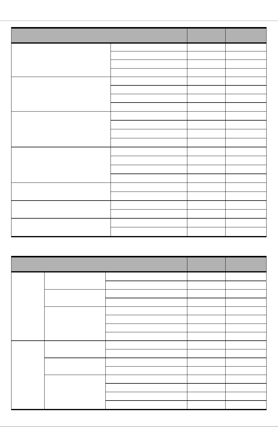
1.3. General Features
The table below summarizes the AirPrime HL8518, HL8528 and HL8529 features.
Table 2. General Features
Feature Description
Physical
Small form factor (146-pin solderable LGA pad) – 23mm x 22mm x 2.5mm
(nominal)
Metal shield can
RF connection pad
Baseband signals connection
Electrical Single or double supply voltage (VBATT and VBATT_PA) – 3.2V – 4.5V
RF
HL8518 (dual-band UMTS and dual-band GSM):
UMTS B1
UMTS B8
E-GSM 900
DCS 1800
HL8528 (dual-band UMTS and dual-band GSM):
UMTS B2
UMTS B5
GSM 850
PCS 1900
HL8529 (dual-band UMTS):
UMTS B2
UMTS B5
Audio interface
Digital interface (ONLY)
Supports Enhanced Full Rate (EFR), Full Rate (FR), Half Rate (HR), and
both Narrow-Band and Wide-band Adaptive Multirate (AMR-NB and AMR-
WB) vocoders
MO and MT calling
Echo cancellation and noise reduction
Emergency calls (112, 110, 911, etc.)
Incoming call notification
DTMF generation

4117047 Rev 2.2 December 18, 2015 11
Product Technical Specification Introduction
Feature Description
SIM interface
Dual SIM Single Standby (DSSS) with fast network switching capability
1.8V/3V support
SIM extraction / hot plug detection
SIM/USIM support
Conforms with ETSI UICC Specifications.
Supports SIM application tool kit with proactive SIM commands
Application interface
NDIS NIC interface support (Windows XP, Windows 7, Windows 8, Windows
CE, Linux)
Multiple non-multiplexed USB channel support
Dial-up networking
USB selective suspend to maximize power savings
CMUX multiplexing over UART
AT command interface – 3GPP 27.007 standard, plus proprietary extended
AT commands
Protocol Stack
Dual-mode UMTS (WCDMA) / HSDPA / HSUPA / EDGE RX / GPRS / GSM
operation
GSM/GPRS/EDGE RX
GPRS Class 12
EDGE RX
CSD (Circuit-switched data bearers)
Release 4 GERAN Feature Package 1
SAIC / DARP Phase 1
Latency Reduction
Repeated FACCH and Repeated SACCH
GPRS ROHC
Enhanced Operator Name String (EONS)
Enhanced Network Selection (ENS)
WCDMA
3GPP WCDMA FDD Multimode Type II UE Protocol Stack
Configurable for data classes up to 384 kBit/s
Inter-RAT Handover and Cell Reselection
Supports two types of Compressed Mode
Network Assisted Cell Change from UTRAN to GERAN and GERAN to
UTRAN
CSD (Circuit-switched data bearers) over WCDMA (transparent/non
transparent up to 64 kBit/s; Support for Video Telephony)
HSDPA (High Speed Downlink Packet Access)
Compliant with 3GPP Release 5
HSDPA Category 8 data rate – 7.2 Mbps (peak rate)
IPv6 support
HSUPA (High Speed Uplink Packet Access)
Compliant with 3GPP Release 6
HSUPA Category 6 data rate - 5.76 Mbps (peak rate)
Robust Header Compression (RoHC)
Fractional DPCH

4117047 Rev 2.2 December 18, 2015 12
Product Technical Specification Introduction
Feature Description
Protocol Stack
HSPA+ (Evolved High Speed Packet Access)
Compliant with 3GPP Release 7
Higher-Order Modulation (HOM)
MAC-ehs support
Continuous Packet Connectivity (CPC)
Enhanced F-DPCH
Enhanced Cell FACH
Circuit Switched Voice over HSPA
SMS
SMS MO and MT
CS and PS support
SMS saving to SIM card or ME storage
SMS reading from SIM card or ME storage
SMS sorting
SMS concatenation
SMS Status Report
SMS replacement support
SMS storing rules (support of AT+CNMI, AT+CNMA)
Supplementary
Services
Call Barring
Call Forwarding
Call Hold
Caller ID
Call Waiting
Multi-party service
USSD
Automatic answer
Connectivity
Multiple (up to 20) cellular packet data profiles
Sleep mode for minimum idle power draw
Automatic GPRS attach at power-up
GPRS detach
Mobile-originated PDP context activation / deactivation
Support QoS profile
Release 97 – Precedence Class, Reliability Class, Delay Class, Peak
Throughput, Mean Throughput
Release 99 QoS negotiation – Background, Interactive, and Streaming
Static and Dynamic IP address. The network may assign a fixed IP address
or dynamically assign one using DHCP (Dynamic Host Configuration
Protocol).
Supports PAP and CHAP authentication protocols
PDP context type (IPv4, IPv6, IPv4v6). IP Packet Data Protocol context
RFC1144 TCP/IP header compression
Interaction with existing GSM services (MO/MT SMS voice calls) while:
GPRS is attached, or
In a GPRS data session (class B GPRS suspend / resume procedures)
Environmental
Operating temperature ranges (industrial grade):
Class A: -30°C to +70°C
Class B: -40°C to +85°C
4117047 Rev 2.2 December 18, 2015 13
Product Technical Specification Introduction
Feature Description
RTC Real Time Clock (RTC) with calendar and alarm
Temperature Sensor
Temperature monitoring
Alarms
1.4. Encryption Support
The AirPrime HL8518, HL8528 and HL8529 supports the following encryption algorithms:
Ciphering algorithms A51, A52 and A53
GEA1/GEA2 and GEA3 algorithm for GPRS encryption
Cyclic Redundancy Check (CRC) with programmable polynomial
UMTS confidentiality algorithm f8 for message ciphering (Kasumi based UEA1)
UMTS integrity algorithm f9 for message authentication (Kasumi based UIA1 and SNOW 3G
based UIA2)
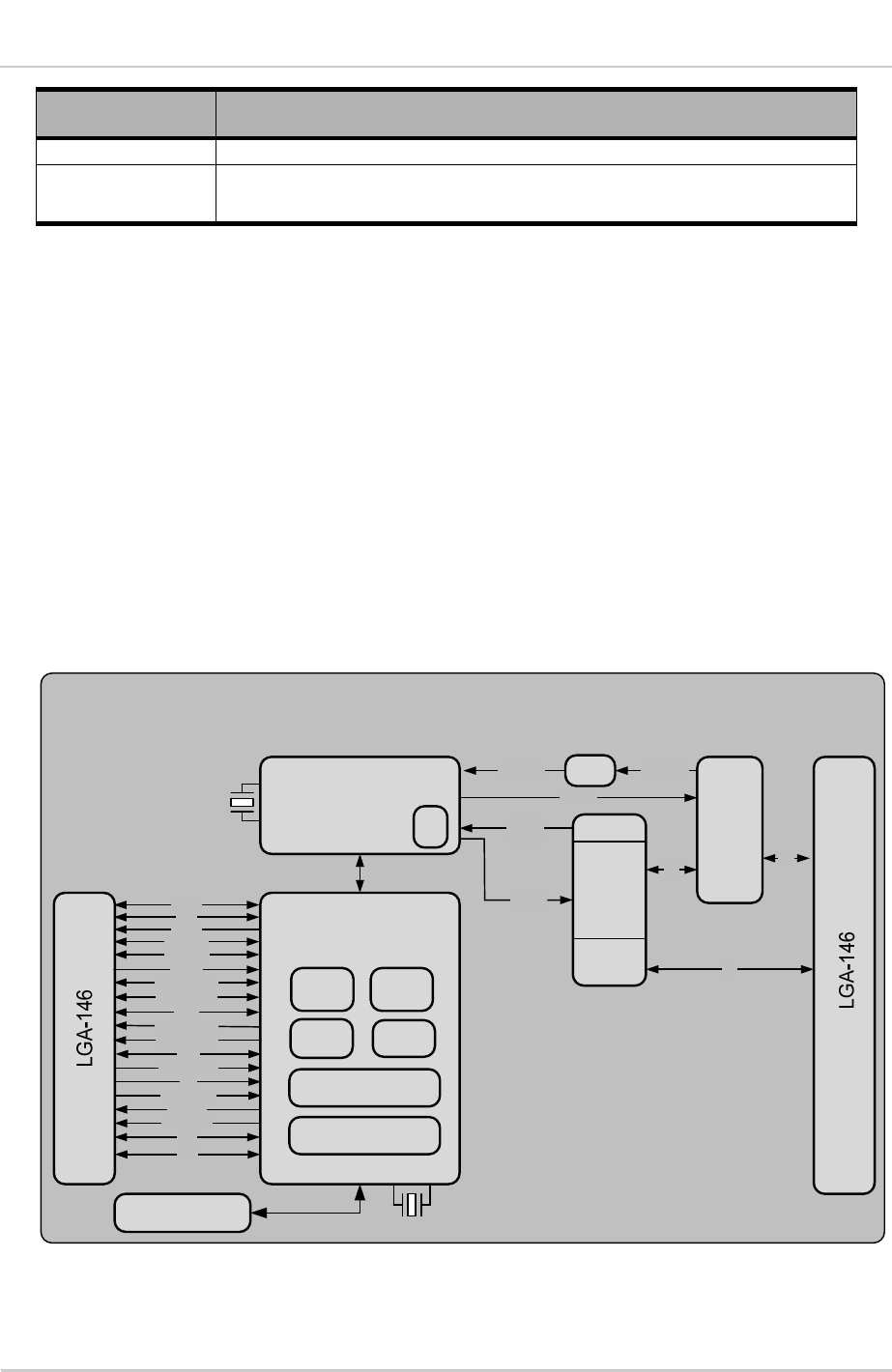
1.5. Architecture
The figure below presents an overview of the AirPrime HL8518, HL8528 and HL8529 modules
internal architecture and external interfaces.
32.768KHz
AirPrime HL8518, HL8528 and HL8529
2G PA
+
Antenna
Switch
26MHz
RF
Baseband
MCU DSP
PMU RF
Analog Baseband
Peripherals
RX_2G
RX_3G
RF
TX_3G
Isoplexer
B1/B8-
GSM900
Or
B2-PCS/B5-
GSM850
Or
B2/B5
Memory
(Flash + RAM)
UART1 (8pins)
Debug (2pins)
VBATT
GND
VGPIO
BAT_RTC
GPIO x 12
ADC x2
RESET_IN_N
JTAG
SIM1
26M_CLKOUT
32K_CLKOUT
TP1
PWR_ON_N
2G_TX_ON
PWM x 2
USB
Transceiver
SAW
Filters
RX_DCS RX_DCS
3G
PA
TX_2G
RF
PCM
Figure 1. Architecture Overview
4117047 Rev 2.2 December 18, 2015 14
Product Technical Specification Introduction
1.6. Interfaces
The AirPrime HL8518, HL8528 and HL8529 modules provide the following interfaces and peripheral
connectivity:
1x – 8-pin UART
1x – Active Low RESET
1x – USB 2.0
1x – Backup Battery Interface
2x – System Clock Out
1x – Active Low POWER ON
1x – 1.8V/3V SIM
1x – Digital Audio
2x – ADC
1x – JTAG Interface
1x – Debug Interface
2x – PWM
12x – GPIOs
1x – 2G TX Burst Indicator
1x – GSM Antenna
1.7. Connection Interface
The AirPrime HL8518, HL8528 and HL8529 modules are an LGA form factor device. All electrical and
mechanical connections are made through the 146 Land Grid Array (LGA) pads on the bottom side of
the PCB.
Figure 2. Mechanical Overview
The 146 pads have the following distribution:
66 inner signal pads, 1x0.5mm, pitch 0.8mm
1 reference test point (Ground), 1.0mm diameter
7 test point (JTAG), 0.8mm diameter, 1.20mm pitch
64 inner ground pads, 1.0x1.0mm, pitch 1.825mm/1.475mm
4 inner corner ground pads, 1x1mm
4 outer corner ground pads, 1x0.9mm
4117047 Rev 2.2 December 18, 2015 15
Product Technical Specification Introduction
1.8. ESD
Refer to the following table for ESD Specifications.
Note: Information specified in the following table is preliminary and subject to change.
Table 3. ESD Specifications
Category Connection Specification
Operational RF ports IEC-61000-4-2 — Level (Electrostatic Discharge Immunity Test)
Non-operational Host connector
interface
Unless otherwise specified:
JESD22-A114 +/- 1kV Human Body Model
JESD22-A115 +/- 200V Machine Model
JESD22-C101C +/- 250V Charged Device Model
Signals
SIM connector ESD protection is highly recommended at the point where the
USIM contacts are exposed, and for any other signals that would
be subjected to ESD by the user.
Other host signals
1.9. Environmental and Certifications
1.9.1. Environmental Specifications
The environmental specification for both operating and storage conditions are defined in the table
below.
Table 4. Environmental Specifications
Conditions Range
Operating Class A -30°C to +70°C
Operating Class B -40°C to +85°C
Storage -40°C to +85°C
Note: The upper limit of Class A is subject to module PCB temperature. A progressive 3G output power
reduction feature is implemented for when PCB temperatures are above +80°C. This leads to a
calibrated 3G TX power output up to +80°C for the PCB temperature and automatic decrease at
higher temperatures. Therefore, depending on module activity and customer design, the upper limit
of Class A could be lower than 70°C.
Class A is defined as the operating temperature ranges that the device:
Shall exhibit normal function during and after environmental exposure.
Shall meet the minimum requirements of 3GPP or appropriate wireless standards.
Class B is defined as the operating temperature ranges that the device:
Shall remain fully functional during and after environmental exposure
Shall exhibit the ability to establish a voice, SMS or DATA call (emergency call) at all times
even when one or more environmental constraint exceeds the specified tolerance.
Unless otherwise stated, full performance should return to normal after the excessive
constraint(s) have been removed.

4117047 Rev 2.2 December 18, 2015 16
Product Technical Specification Introduction
1.9.2. Regulatory
The AirPrime HL8518, HL8528 and HL8529 modules are compliant with the following regulations:
R&TTE directive 1999/5/EC
FCC
IC
These compliances will be reflected on the AirPrime HL8518, HL8528 and HL8529 modules labels
when applicable.
1.9.3. RoHS Directive Compliant
The AirPrime HL8518, HL8528 and HL8529 modules are compliant with RoHS Directive 2011/65/EU
which sets limits for the use of certain restricted hazardous substances. This directive states that
“from 1st July 2006, new electrical and electronic equipment put on the market does not contain lead,
mercury, cadmium, hexavalent chromium, polybrominated biphenyls (PBB) or polybrominated
diphenyl ethers (PBDE)”.
1.9.4. Disposing of the Product
This electronic product is subject to the EU Directive 2012/19/EU for Waste Electrical
and Electronic Equipment (WEEE). As such, this product must not be disposed of at a
municipal waste collection point. Please refer to local regulations for directions on how
to dispose of this product in an environmental friendly manner.
1.10. References
[1] AirPrime HL Series Customer Process Guidelines
Reference Number: 4114330
[2] AirPrime HL6 and HL8 Series AT Commands Interface Guide
Reference Number: 4114680
[3] AirPrime HL Series Dual SIM Single Standby Application Note
Reference Number: 2174034
4117047 Rev 2.2 December 18, 2015 17
2. Detailed Interface Specifications
Note: If not specified, all electrical values are given for VBATT=3.7V and an operating temperature of
25°C.
For standard applications, VBATT and VBATT_PA must be tied externally to the same power
supply. For some specific applications, AirPrime HL8518, HL8528 and HL8529 modules support
separate VBATT and VBATT_PA connection if requirements below are fulfilled.
2.1. Power Supply
The AirPrime HL8518, HL8528 and HL8529 modules are supplied through the VBATT signal.
2.1.1. Electrical Characteristics
The following table describes the electrical characteristics of the Power Supply interface.
Table 5. Power Supply
Supply Minimum Typical Maximum
VBATT voltage (V) 3.21 3.7 4.5
VBATT_PA voltage (V) Full Specification 3.21 3.7 4.5
VBATT_PA voltage (V) Extended Range 2.82 3.7 4.5
1 This value has to be guaranteed during the burst
2 No guarantee of 3GPP performances over extended range
Note: Load capacitance for VBATT is around 30µF ± 20% embedded inside the module.
Load capacitance for VBATT_PA is around 20µF ± 20% embedded inside the module.
2.1.2. Pin Description
The following table describes the pin description of the Power Supply interface.
Table 6. Power Supply Pin Description
Pin Number Signal Name I/O Description
63 VBATT I Power supply (base band)
61, 62 VBATT_PA I Power supply (radio frequency)
37, 39, 48, 67-70, 167-234 GND Ground

4117047 Rev 2.2 December 18, 2015 18
Product Technical Specification Detailed Interface Specifications
2.1.3. Burst Transmission Current Requirements
The power supply must be able to deliver high current peaks in a short time due to the burst
transmission nature of GSM. For supply filtering recommendations, please refer to section 2.3
Decoupling of Power Supply Signals.
The following table describes radio burst rates in connected mode. For detailed power consumption
figures, refer to section 2.4 Current DC Power Consumption.
Table 7. Radio Burst Rates – Connected Mode
GSM/GPRS
Multislot Class
RF Power
Amplifier Current Slot Duration Period Rising Time
Class 10 2.2A peak 577 μs 4.615 ms 10 μs
Class 12
The corresponding radio burst rates in connected mode are as follows:
GSM/GPRS class 2 terminals emit 577 µs radio bursts every 4.615 ms
GPRS class 10 terminals emit 1154 µs radio bursts every 4.615 ms
GPRS class 12 terminals emit 2308 µs radio bursts every 4.615 ms
In connected mode, the RF Power Amplifier current (2.2A peak in GSM /GPRS mode) flows with a
ratio of:
1/8 of the time (around 577 µs every 4.615 ms for GSM /GPRS cl 2 – 2RX/1TX), and
4/8 of the time (around 2308 µs every 4.615 ms for GSM /GPRS cl 12 – 4RX/1TX) with the
rising time at around 10 µs.
Figure 3. Power Supply During Burst Transmission
4117047 Rev 2.2 December 18, 2015 19
Product Technical Specification Detailed Interface Specifications
2.1.4. Power Input (VBATT)
An external power supply uses the VBATT pins to:
Supply the AirPrime HL8518, HL8528 and HL8529 modules.
Directly supply the RF components.
It is essential to keep the voltage ripple to a minimum at this connection to avoid any
phase error or spectrum modulation degradation.
An inadequate power supply can significantly affect RF performance (TX power,
modulation spectrum, EMC performance, spurious emission, frequency error, etc.).
Provide reference voltage VGPIO (through internal regulators) for the baseband signals.
When the AirPrime HL8518, HL8528 and HL8529 modules are supplied with a battery, the total
impedance (battery + protections + PCB) should be such that the supply will be >= 3.2 V during GSM
burst mode operation drawing a maximum peak current of 2.2 A for 577 µs (one slot) or 1154 µs (two
slots) TX.
2.2. Ground Connection
The AirPrime HL8518, HL8528 and HL8529 modules shielding case is the grounding. The ground
must be connected on the motherboard through a complete layer on the PCB.
The ground connection is made by soldering the LGA ground pins and rectangular ground pad to the
ground plane of the application board.
2.3. Decoupling of Power Supply Signals
The ETSI standard defines specific requirements for phase error and spectrum modulation. Both are
mandatory and can be affected by the choice of power supply filtering. It is highly recommended to
provide multiple capacitor values to solve an eventual Amplitude and Phase Modulation issue.
AirPrime HL8518, HL8528 and HL8529 modules already here embedded decoupling capacitors on
the VBATT lines, but additional external decoupling may be required.
EMI/RFI issues – Add a capacitor (10pF~33pF) close to the VBATT pins.
TDMA noise (217 Hz) – Place a low ESR decoupling capacitors (at least 100 µF) as close to
the module as possible to reduce noise.
Figure 4. Power Supply Requirements
4117047 Rev 2.2 December 18, 2015 20
Product Technical Specification Detailed Interface Specifications
The figure below shows the power supply voltage drop shapes during GSM 2G transmission.
Figure 5. Power Supply Voltage Drops Shapes During Burst Transmission
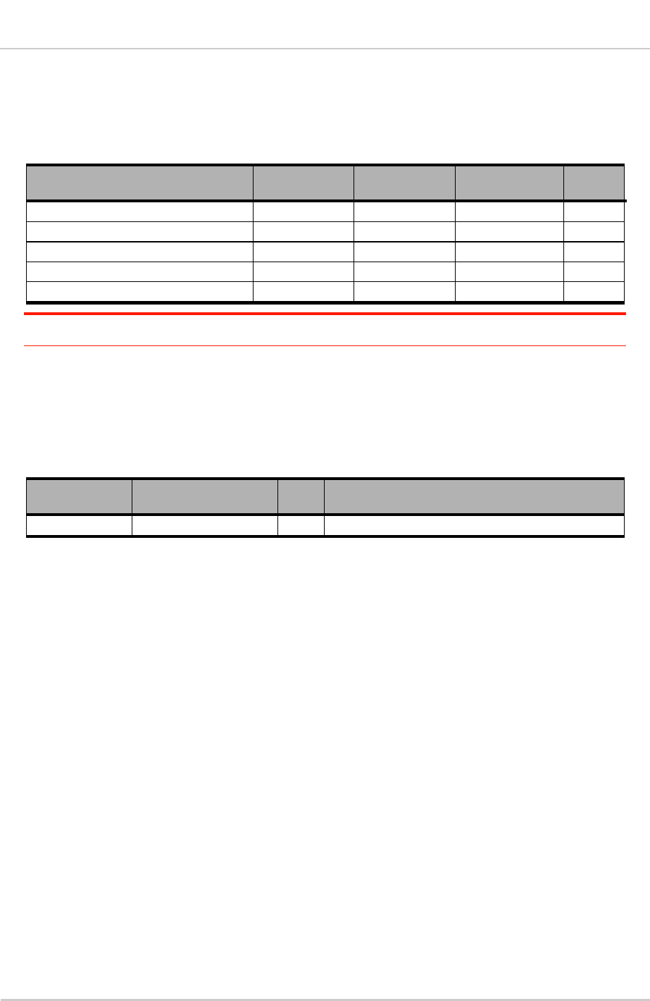
2.4. Current DC Power Consumption
The following table lists the current consumption of the AirPrime HL8518, HL8528 and HL8529
modules at different conditions.
Note: The following data is under the setup recommended in section 3.5 Power Supply Design.
The USB is disconnected for the lowest current consumption.
Typical values are measured at ambient temperature, and maximum values are measured over the
entire operating temperature range. (The measurements are done with a CMU200 and with a 50Ω
load.) For a description of input voltage requirements, see section 2.1 Power Supply.
Table 8. Current Consumption (at nominal voltage, 3.7V)
Parameters Typical Maximum
Off mode 50 µA
Sleep mode - GSM DRX2
(registered to the network)
GSM900 1.5 mA 3.15 mA
DCS1800 1.5 mA 3.15 mA
GSM850 1.6 mA 3.4 mA
PCS1900 1.6 mA 3.4 mA
Sleep mode - GSM DRX9
(registered to the network)
GSM900 1.15 mA 2.7 mA
DCS1800 1.0 mA 2.7 mA
GSM850 1.3 mA 2.9 mA
PCS1900 1.25 mA 2.95 mA
Sleep mode - WCDMA DRX6
(registered to the network)
Band 1 1.75 mA 3.45 mA
Band 2 2 mA 3.75 mA
Band 5 2 mA 3.8 mA
Band 8 1.75 mA 3.5 mA
4117047 Rev 2.2 December 18, 2015 21
Product Technical Specification Detailed Interface Specifications
Parameters Typical Maximum
Sleep mode - WCDMA DRX9
(registered to the network)
Band 1 1.1 mA 2.7 mA
Band 2 1.3 mA 2.9 mA
Band 5 1.3 mA 3.2 mA
Band 8 1.1 mA 2.7 mA
WCDMA in communication mode
(Voice Call)
Band 1 620 mA 735 mA
Band 2 620 mA 735 mA
Band 5 500 mA 650 mA
Band 8 500 mA 650 mA
WCDMA in communication mode
(HSDPA)
Band 1 700 mA 880 mA
Band 2 680 mA 900 mA
Band 5 550 mA 760 mA
Band 8 580 mA 800 mA
WCDMA in communication mode
(HSUPA)
Band 1 700 mA 880 mA
Band 2 665 mA 900 mA
Band 5 550 mA 760 mA
Band 8 580 mA 800 mA
GSM in communication mode GSM900 / GSM850 (PCL=5) 220 mA 250 mA
DCS / PCS (PCL=0) 165 mA 175 mA
GPRS (2 TX,3 RX) GSM900 / GSM850 (PCL=5) 425 mA 460 mA
DCS / PCS (PCL=0) 300 mA 335 mA
Peak current consumption GSM900 / GSM850 1.9 A 2.2A
DCS / PCS 1.8 A 2.0A
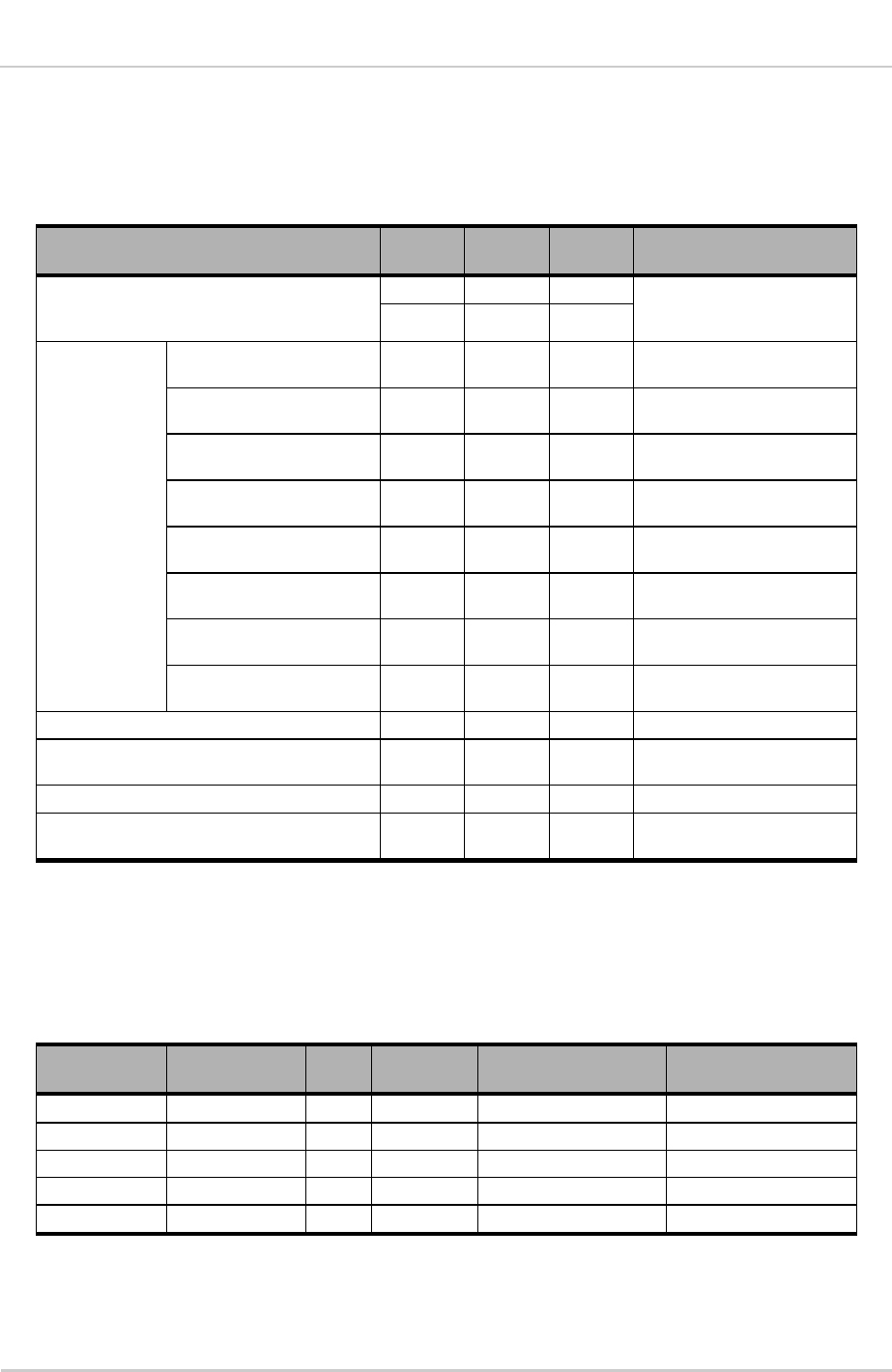
Table 9. Current Consumption per Power Supply (VBATT_PA and VBATT)
Parameters Typical Maximum
VBATT_PA
Average current GSM in
communication mode
E-GSM 900 / GSM 850 (PCL=5) 185 mA 210 mA
DCS 1800/ PCS 1900 (PCL=0) 130 mA 135 mA
Average current
GPRS (2 TX,3 RX)
E-GSM 900 / GSM 850 (PCL=5) 370 mA 395 mA
DCS 1800/ PCS 1900 (PCL=0) 245 mA 270 mA
Average current
WCDMA in
communication mode
(Voice Call)
Band 1 520 mA 615 mA
Band 2 520 mA 615 mA
Band 5 405 mA 530 mA
Band 8 405 mA 530 mA
VBATT
Average current GSM in
communication mode
E-GSM 900 / GSM 850 (PCL=5) 35 mA 40 mA
DCS 1800/ PCS 1900 (PCL=0) 35 mA 40 mA
Average current
GPRS (2 TX,3 RX)
E-GSM 900 / GSM 850 (PCL=5) 55 mA 65 mA
DCS 1800/ PCS 1900 (PCL=0) 55 mA 65 mA
Average current
WCDMA in
communication mode
(Voice Call)
Band 1 100 mA 120 mA
Band 2 100 mA 120 mA
Band 5 95 mA 120 mA
Band 8 95 mA 120 mA
4117047 Rev 2.2 December 18, 2015 22
Product Technical Specification Detailed Interface Specifications
2.5. VGPIO
The VGPIO output can be used to:
Pull-up signals such as I/Os
Supply the digital transistors driving LEDs
Act as a voltage reference for the ADC interfaces, ADC0 and ADC1
The VGPIO output is available when the AirPrime HL8518, HL8528 and HL8529 module is switched
ON.
2.5.1. Electrical Characteristics
The following table describes the electrical characteristics of the VGPIO interface.
Table 10. VGPIO Electrical Characteristics
Parameter Min Typ Max Remarks
Voltage level (V) 1.7 1.8 1.9 Both active mode and sleep mode
Current capability active
mode (mA) - - 50 Power Management support up to 50mA output.
Rise Time(ms) - - 1.5 Start-Up time from 0V
2.5.2. Pin Description
The following table describes the pin description of the VGPIO interface.
Table 11. VGPIO Pin Description
Pin Number Signal Name I/O I/O Type Function
45 VGPIO O 1.8V (Power supply) GPIO voltage output
2.6. BAT_RTC
The AirPrime HL8518, HL8528 and HL8529 modules provide an input/output to connect a Real Time
Clock power supply.
This pin is used as a back-up power supply for the internal Real Time Clock. The RTC is supported
when VBATT is available but a back-up power supply is needed to save date and hour when VBATT
is switched off.
If VBATT is available, the back-up battery can be charged by the internal 1.8V power supply regulator.
4117047 Rev 2.2 December 18, 2015 23
Product Technical Specification Detailed Interface Specifications
2.6.1. Electrical Characteristics
The following table describes the electrical characteristics of the BAT_RTC interface.
Table 12. BAT_RTC Electrical Characteristics
Parameter Minimum Typical Maximum Unit
Input voltage -5% 1.8 +5% V
Input current consumption - 2.5 - µA
Output current capability 7 - - mA
Output voltage -5% 1.8 +5% V
Max charging current (@VBATT=3.7V) - 25 - mA
Note: When used with the HL Series snap-in socket, or when compatibility with HL6528x is needed,
Sierra Wireless recommends adding a 10µF capacitor to the BAT_RTC pin.
2.6.2. Pin Description
The following table describes the pin description of the BAT_RTC interface.
Table 13. BAT_RTC Pin Description
Pin Number Signal Name I/O Function
21 BAT_RTC I/O Power supply for RTC backup
2.7. SIM Interface
The AirPrime HL8518, HL8528 and HL8529 modules have one physical SIM interface, UIM1, which
has optional support for dual SIM application with an external SIM switch. Refer to Section 3.8 Dual
SIM Application for more information regarding dual SIM.
The UIM1 interface allows control of a 1.8V/3V SIM and is fully compliant with GSM 11.11
recommendations concerning SIM functions.
The five signals used by this interface are as follows:
UIM1_VCC: power supply
UIM1_CLK: clock
UIM1_DATA: I/O port
UIM1_RST: reset
UIM1_DET:SIM detection (optional)
4117047 Rev 2.2 December 18, 2015 24
Product Technical Specification Detailed Interface Specifications
2.7.1. Electrical Characteristics
The following table describes the electrical characteristics of the UIM1 interface.
Table 14. Electrical Characteristics of UIM1
Parameter Min Typ Max Remarks
UIM1 Interface Voltage : (V)
( VCC, CLK, IO, RST )
2.7 3.0 3.15 The appropriate output
voltage is auto detected
and selected by software.
1.65 1.80 1.95
UIM1 Interface
Voltage: (V)
(VCC, CLK,
IO, RESET )
VIH : Input Voltage-High
(VDD=1.8V) VDD*0.7 - 1.95
VIL : Input Voltage-Low
(VDD=1.8V) 0 - VDD*0.2
VOH : Output Voltage-High
(VDD=1.8V) VDD*0.7 - 1.95
VOL : Output Voltage-Low
(VDD=1.8V) 0 - VDD*0.2
VIH : Input Voltage-High
(VDD=3.0V) VDD*0.7 - 3.15
VIL : Input Voltage-Low
(VDD=3.0V) 0 - VDD*0.2
VOH : Output Voltage-High
(VDD=3.0V) VDD*0.7 - 3.15
VOL : Output Voltage-Low
(VDD=3.0V) 0 - VDD*0.2
UIM1 DET 1.33 1.80 2.1 High active
UIM1_VCC Current (mA) - - 10 Max output current in sleep
mode = 3 mA
UIM1_VCC Line Regulation (mV/V) - - 50 At Iout Max.
UIM1_VCC Power-up Setting Time (µs)
from power down - 10 -
2.7.2. Pin Description
The following table describes the pin description of the UIM1 interface.
Table 15. UIM1 Pin Description
Pin Number Signal Name I/O I/O Type Function Multiplex
26 UIM1_VCC O 1.8V/3V UIM1 Power supply
27 UIM1_CLK O 1.8V/3V UIM1 Clock
28 UIM1_DATA I/O 1.8V/3V UIM1 Data
29 UIM1_RESET O 1.8V/3V UIM1 Reset
64 UIM1_DET I 1.8V UIM1 detection GPIO3
4117047 Rev 2.2 December 18, 2015 25
Product Technical Specification Detailed Interface Specifications
2.7.3. UIM1_DET
UIM1_DET is used to detect and notify the application about the insertion and removal of a SIM
device in the SIM socket connected to the main SIM interface (UIM1). When a SIM is inserted, the
state of UIM1_DET transitions from logic 0 to logic 1. Inversely, when a SIM is removed, the state of
UIM1_DET transitions from logic 1 to logic 0.
The GPIO used for UIM1_DET is GPIO3.
Enabling or disabling this SIM detect feature can be done using the AT+KSIMDET command. For more
information about this command, refer to document [2] AirPrime HL6 and HL8 Series AT Commands
Interface Guide.
2.7.4. Application
2.7.4.1. Reference Schematic
Figure 6. UIM1 Application Reference Schematic
2.7.4.2. USIM Socket Pin Description
The following table describes the required USIM socket pins.
Table 16. USIM Socket Pin Description
Pin Number Signal Name Description
1 UIM1_VCC UIM1 Power supply
2 UIM1_RESET UIM1 Reset
3 UIM1_CLK UIM1 Clock
4 UIM1_DET UIM1 detection
5 GROUND GND
6 - -
7 UIM1_DATA UIM1 Data
8 VGPIO Power supply

4117047 Rev 2.2 December 18, 2015 26
Product Technical Specification Detailed Interface Specifications
2.8. USB
The AirPrime HL8518, HL8528 and HL8529 modules have one USB interface.
2.8.1. Electrical Characteristics
The following table describes the electrical characteristics of the USB interface.
Table 17. Electrical Characteristics of USB
Signal I/O I/O Type Parameter Min. Typ. Max. Unit
USB_D+ I/O Analog 3.06 3.3 3.6 V
USB_D- I/O Analog 3.06 3.3 3.6 V
USB data
(DP, DM) I/O Analog
VIH: Input Voltage-High 2 - 3.2 V
VIL: Input Voltage-Low -0.3 - 0.8 V
VOL: Static Output Voltage-Low - - 0.45 V
VOH: Static Output Voltage-High 2.45 - - V
USB_VBUS I Analog Voltage input 4.75 5.0 5.25 V
USB_VBUS Input current consumption mA
2.8.2. Pin Description
The following table describes the pin description of the USB interface.
Table 18. USB Pin Description
Pin Number Signal Name I/O I/O Type Function
12 USB_D- I/O 3.3V USB data negative line pad
13 USB_D+ I/O 3.3V USB data positive line pad
16 USB_VBUS I 5V USB VBUS
Note: When the 5V USB supply is not available, connect USB_VBUS to VBATT to supply the USB
interface.
2.9. Electrical Information I/O
The AirPrime HL8518, HL8528 and HL8529 modules support different groups of digital interfaces with
varying current drain limits. The following table enumerates these interface groupings and enumerates
the electrical characteristics of each digital interface.
The DC characteristics of the pads are compatible with CMOS JEDEC standard EIA/JESD8-5.
Table 19. Digital I/O Electrical Characteristics
Parameter Min Typ Max Conditions
VIL: Input voltage for general digital pad (V) -0.2 - VDD*0.2

4117047 Rev 2.2 December 18, 2015 27
Product Technical Specification Detailed Interface Specifications
Parameter Min Typ Max Conditions
VIH: Input voltage for general digital pad (V) VDD*0.7 - VDD + 0.2
Input / Output leakage Current (µA) - - ±0.7
VDD (V) 1.7 1.8 1.9
Driver Pad Class A
VOLA: Output Voltage-Low (V) - - 0.2 IOL = + 0.1mA
- - 0.35 IOL = +6.0mA
VOHA: Output Voltage-High (V) VDD-0.35 - - IOH = - 6.0mA
VDD-0.2 - - IOH = - 0.1mA
Driver Pad Class B
VOLB: Output Voltage-Low (V) - - 0.2 IOL = + 0.1mA
- - 0.35 IOL = +4.0 mA
VOHB: Output Voltage-High (V) VDD-0.35 - - IOH = - 4.0mA
VDD-0.2 - - IOH = - 0.1mA
Driver Pad Class C
VOLC: Output Voltage-Low (V) - - 0.2 IOL = + 0.1mA
- - 0.35 IOL = +2.0mA
VOHC: Output Voltage-High (V) VDD-0.35 - - IOH = - 2.0mA
VDD-0.2 - - IOH = - 0.1mA
Driver Pad Class D
VOLD: Output Voltage-Low (V) - - 0.2 IOL = + 0.1mA
- - 0.35 IOL = +1.0mA
VOHD: Output Voltage-High (V) VDD-0.35 - - IOH = - 1.0mA
VDD-0.2 - - IOH = - 0.1mA
Driver Pad Class E
VOLE: Output Voltage-Low (V) - - 0.2 IOL = + 0.1mA
- - 0.35 IOL = +1.0mA
VOHE: Output Voltage-High (V) VDD-0.35 - - IOH = - 1.0mA
VDD-0.2 - - IOH = - 0.1mA
2.10. General Purpose Input/Output (GPIO)
The AirPrime HL8518, HL8528 and HL8529 modules provide 12 GPIOs, 2 of which have multiplexes.
Table 20. GPIO Pin Description
Pin Number Signal Name Multiplex I/O Power Supply Domain
1 GPIO1 I/O 1.8V
10 GPIO2* I/O 1.8V
40 GPIO7 I/O 1.8V
41 GPIO8 I/O 1.8V
46 GPIO6 I/O 1.8V
52 GPIO10 I/O 1.8V
4117047 Rev 2.2 December 18, 2015 28
Product Technical Specification Detailed Interface Specifications
Pin Number Signal Name Multiplex I/O Power Supply Domain
53 GPIO11 I/O 1.8V
54 GPIO15 I/O 1.8V
58 GPIO12 PWM2 I/O 1.8V
64 GPIO3 UIM1_DET I/O 1.8V
65 GPIO4 I/O 1.8V
66 GPIO5 I/O 1.8V
* This pin can be used to trigger the module to wake up from Sleep Mode.
2.11. Main Serial Link (UART1)
The main serial link (UART1) is used for communication between the AirPrime HL8518, HL8528 and
HL8529 modules and a PC or host processor. It consists of a flexible 8-wire serial interface that
complies with RS-232 interface.
The supported baud rates of the UART1 are 300, 1200, 2400, 4800, 9600, 19200, 38400, 57600,
115200, 230400, 460800, 500000, 750000, 921600, 1843200, 3000000, 3250000 and 6000000 bit/s.
The signals used by UART1 are as follows:
TX data (UART1_TX)
RX data (UART1_RX)
Request To Send (UART1_RTS)
Clear To Send (UART1_CTS)
Data Terminal Ready (UART1_DTR)
Data Set Ready (UART1_DSR)
Data Carrier Detect (UART1_DCD)
Ring Indicator (UART1_RI)
Note: Signal names are according to PC view.
2.11.1. Pin Description
The following table describes the pin description of the UART1 interface.
Table 21. UART1 Pin Description
Pin # Signal Name* I/O* Description
2 UART1_RI O Signal incoming calls (voice and data), SMS, etc.
3 UART1_RTS I Wakes the module up when AT+KSLEEP=1 is used
4 UART1_CTS O Ready to receive AT commands
5 UART1_TX I Transmit data
6 UART1_RX O Receive data
7 UART1_DTR I
(active low)
Prevents the module from entering sleep mode, switches between
data mode and command mode, and wakes the module up.
8 UART1_DCD O Signal data connection in progress
9 UART1_DSR O Signal UART interface is ON
* According to PC view.
4117047 Rev 2.2 December 18, 2015 29
Product Technical Specification Detailed Interface Specifications
2.11.2. 8-wire Application
Figure 7. 8-wire UART Application Example
2.11.3. 4-wire Application
Figure 8. 4-wire UART Application Example
2.11.4. 2-wire Application
Figure 9. 2-wire UART Application Example
4117047 Rev 2.2 December 18, 2015 30
Product Technical Specification Detailed Interface Specifications
2.12. POWER ON Signal (PWR_ON_N)
A low level signal has to be provided to switch the AirPrime HL8518, HL8528 and HL8529 modules
ON.
It is internally connected to the permanent 1.8V supply regulator inside the HL8518, HL8528 and
HL8529 via a pull-up resistor. Once VBAT is supplied to the module, this 1.8V supply regulator will be
enabled and so the PWR_ON_N signal is by default at high level.
The PWR_ON_N signal’s characteristics are listed in the table below.
Table 22. PWR_ON_N Electrical Characteristics
Parameter Min Typical Max
Input Voltage-Low (V) - 0.51
Input Voltage-High (V) 1.33 - 2.2
Power-up period (ms) from PWR_ON_N falling edge 2000 - -
PWR_ON_N assertion time (ms) 25
Note: As PWR_ON_N is internally pulled up with 200kΩ, a simple open collector or open drain transistor
must be used for ignition.
The software starts operating when the module is ON, but “AT Command Ready” will depend on
whether UART or USB is used.
Figure 10. PWR_ON_N Assertion Time
VGPIO is an output from the module that can be used to check if the module is active.
When VGPIO = 0V, the module is OFF.
When VGPIO = 1.8V, the module is ON (it can be in idle, communication or sleep mode)
Note: PWR_ON_N cannot be used to power the module off. To power the module off, use AT command
AT+CPOF.
2.13. Reset Signal (RESET_IN_N)
To reset the module, a low level pulse must be sent on the RESET_IN_N pin for 10ms. This action will
immediately restart the AirPrime HL8518, HL8528 and HL8529 modules with the PWR_ON_N signal
at low level. (If the PWR_ON_N signal is at high level, the module will be powered off.) As
RESET_IN_N is internally pulled up, a simple open collector or open drain transistor can be used to
control it.
The RESET_IN_N signal will reset the registers of the CPU and reset the RAM memory as well, for
the next power on.

4117047 Rev 2.2 December 18, 2015 31
Product Technical Specification Detailed Interface Specifications
Note: As RESET_IN_N is referenced to the VGPIO domain (internally to the module), it is impossible to
reset before the module starts or to try to use RESET_IN_N as a way to start the module.
Another more costly solution would be to use MOS transistor to switch the power supply off and
restart the power up procedure using the PWR_ON_N input line.
Table 23. RESET_IN_N Electrical Characteristics
Parameter Min Typical Max
Input Voltage-Low (V) - 0.51
Input Voltage-High (V) 1.33 - 2.2
Power-up period (ms) from RESET_IN_N falling edge* 2000 - -
* With the PWR_ON_N Signal at low level
4117047 Rev 2.2 December 18, 2015 32
3. Design Guidelines
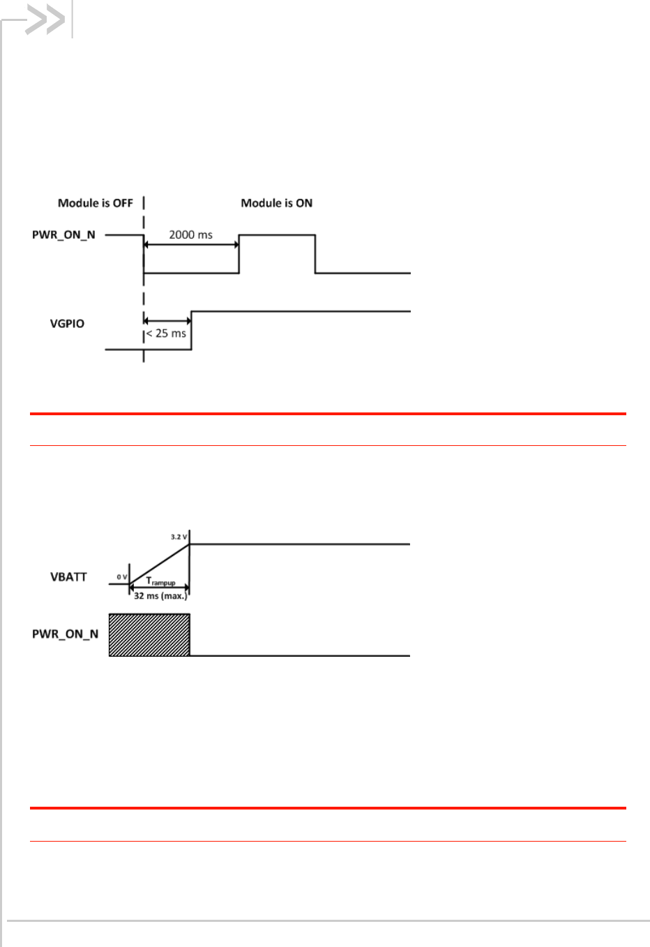
3.1. Power-Up Sequence
Apply a LOW level logic to the PWR_ON_N pin (pin 59); within 25ms, VGPIO will appear to be at
1.8V. Either a USB or UART1 interface could be used to send AT commands. Note that for USB
connections, the time when AT commands can be sent will depend on the initialization time used for
the USB connection with the USB host.
Figure 11. PWR_ON_N Sequence with VGPIO Information
Note: As PWR_ON_N is internally pulled up with 200kΩ, a simple open collector or open drain transistor
must be used for ignition.
The PWR_ON_N pin has the minimum assertion time requirement of 25ms, with LOW active. Once
the valid power on trigger is detected, the PWR_ON_N pin status can be left open.
VBATT has to ramp up within 32 ms to reach the value of 3.2V; otherwise, the module may not power
up.
Figure 12. PWR_ON_N Sequence with Trampup
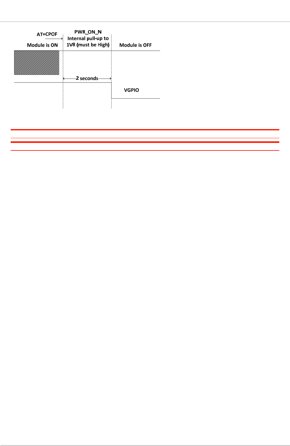
3.2. Module Switch-Off
AT command AT+CPOF enables the user to properly switch the AirPrime HL8518, HL8528 and
HL8529 modules off. The PWR_ON signal must be set to high (inactive) before the AT+CPOF
command is sent.
Note: If the PWR_ON signal is active (low level) when the AT+CPOF command is sent, the module will
not power off.
If required, the module can be switched off by controlling the power supply. This can be used, for
example, when the system freezes and no reset line is connected to the AirPrime HL8518, HL8528
and HL8529 modules. In this case, the only way to get control over the module back is to switch off
the power line.
4117047 Rev 2.2 December 18, 2015 33
Product Technical Specification Design Guidelines
Figure 13. Power OFF Sequence for PWR_ON_N, VGPIO
Note: PWR_ON_N is internally pulled up by 200kΩ to 1.8V.
Caution: Ensure that no external pull-ups are applied on IO pins while the module is OFF.
3.3. Emergency Power OFF
If required, the module can be switched off by controlling the RESET_IN_N pin (pin 11). This must
only be used in emergency situations if the system freezes (not responding to AT commands).
To perform an emergency power off, a low level pulse must be sent on the RESET_IN_N pin for 10ms
while the PWR_ON signal is inactive (high level). This action will immediately shut the HL8518,
HL8528 and HL8529 modules down and the registers of the CPU and RAM memory will be reset for
the next power on.
3.4. Sleep Mode Management
3.4.1. Using UART
AT command AT+KSLEEP enables sleep mode configuration.
AT+KSLEEP=0:
The module is active when DTR signal is active (low electrical level).
When DTR is deactivated (high electrical level), the module will enter sleep mode after a
while.
On DTR activation (low electrical level), the module wakes up.
AT+KSLEEP=1:
The module determines when it enters sleep mode (when no more tasks are running).
“0x00” character on the serial link wakes the module up.
AT+KSLEEP=2:
The module never enters sleep mode.
3.4.2. Using USB
Use AT+KSLEEP=1 to allow the module to automatically enter sleep mode while the USB interface is
in use.
4117047 Rev 2.2 December 18, 2015 34
Product Technical Specification Design Guidelines
3.5. Power Supply Design
The AirPrime HL8518, HL8528 and HL8529 modules should not be supplied with voltage over 4.5V
even temporarily or however briefly.
If the system’s main board power supply unit is unstable or if the system’s main board is supplied with
over 4.5V, even in the case of transient voltage presence on the circuit, the module’s power amplifier
may be severely damaged.
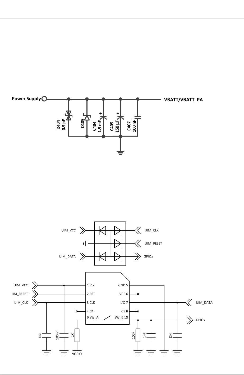
To avoid such issues, add a voltage limiter to the module’s power supply lines so that VBATT and
VBATT_PA signal pads will never receive a voltage surge over 4.5V. The voltage limiter can be as
simple as a Zener diode with decoupling capacitors as shown in the diagram below.
Figure 14. Voltage Limiter Example
3.6. ESD Guidelines for SIM Card
Decoupling capacitors must be added as close as possible to the SIM card connectors on UIM1_CLK,
UIM1_RST, UIM1_VCC and UIM1_DATA signals to avoid EMC issues and to pass the SIM card type
approval tests, according to the drawings below.
A typical schematic for hardware SIM detection is provided below.
Figure 15. EMC and ESD Components Close to the SIM
4117047 Rev 2.2 December 18, 2015 35
Product Technical Specification Design Guidelines
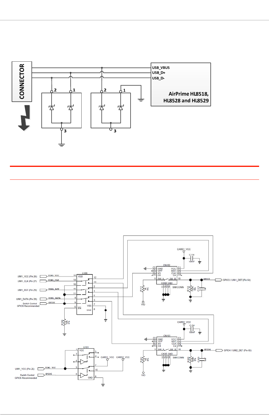
3.7. ESD Guidelines for USB
When the USB interface is externally accessible, it is required to have ESD protection on the
USB_VBUS, USB_D+ and USB_D- signals.
Figure 16. ESD Protection for USB
Note: It is not recommended to have an ESD diode with feedback path from USB_VBUS to either
USB_D+ or USB_D-.
3.8. Dual SIM Application
Using an external switch and GPIOs, the AirPrime HL8518, HL8528 and HL8529 modules can
support Dual SIM Single Standby with fast network switching. Refer to document [2] AirPrime HL6
and HL8 Series AT Commands Interface Guide for related AT commands.
Figure 17. Reference Design for Dual SIM Application
4117047 Rev 2.2 December 18, 2015 36
Product Technical Specification Design Guidelines
3.9. Radio Frequency Integration
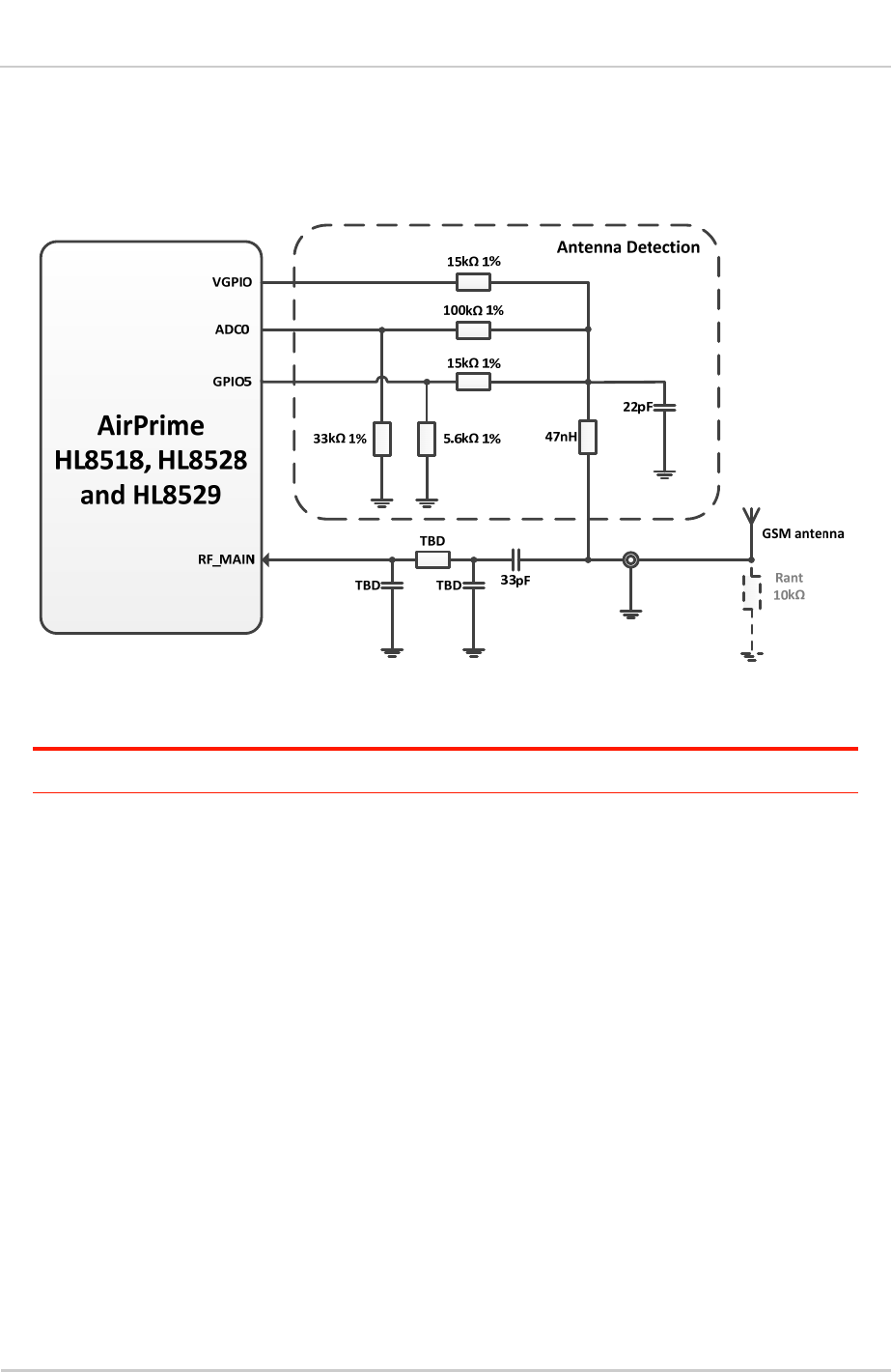
The AirPrime HL8518, HL8528 and HL8529 modules are equipped with an external antenna. A 50Ω
line matching circuit between the module, the customer’s board and the RF antenna is required, for
GSM feed path, as shown in the example below.
Figure 18. GSM Antenna Connection with Antenna Detection
Note: Antenna detection circuit is optional. Rant is the equivalent DC terminating resistor of the antenna.
Rant should be close to 10KΩ.

4117047 Rev 2.2 December 18, 2015 37
4. Regulatory Legal Information
4.1. Label
The AirPrime HL852x module is labeled with its own FCC ID on the shield side. Each HL852x variant
has its own FCC ID as listed in the table below.
Table 24. AirPrime HL852x FCC IDs
Model Name FCC ID
HL8528 N7NHL8528
HL8529 N7NHL8529
When the module is installed in a customer’s product, the FCC ID label on the module will not be
visible. To avoid this case, an exterior label must be stuck on the surface of the customer’s product to
indicate the FCC ID of the enclosed module. This label can use wording such as the following:
“Contains Transmitter module FCC ID: <FCC ID as listed in Table 24 AirPrime HL852x FCC IDs>” or
“Contains FCC ID: <FCC ID as listed in Table 24 AirPrime HL852x FCC IDs>”.
4.2. FCC Regulations
This device complies with part 15 of the FCC Rules. Operation is subject to the following two
conditions:
1. This device may not cause harmful interference, and
2. This device must accept any interference received, including interference that may cause
undesired operation.
This device has been tested and found to comply with the limits for a Class B digital device, pursuant
to Part 15 of the FCC Rules. These limits are designed to provide reasonable protection against
harmful interference in a residential installation. This equipment can radiate radio frequency energy
and, if not installed and used in accordance with the instructions, may cause harmful interference to
radio communications. However, there is no guarantee that interference will not occur in a particular
installation. If this equipment does cause harmful interference to radio or television reception, which
can be determined by turning the equipment off and on, the user is encouraged to try to correct the
interference by one or more of the following measures:
1. Reorient or relocate the receiving antenna
2. Increase the separation between the equipment and receiver.
3. Connect the equipment into an outlet on a circuit different from that to which the receiver
is connected.
4. Consult the dealer or an experienced radio/TV technician for help.
Changes or modifications not expressly approved by the party responsible for compliance could void
the user’s authority to operate the equipment.

4117047 Rev 2.2 December 18, 2015 38
Product Technical Specification Regulatory Legal Information
4.3. RF Exposure Information
This Modular Approval is limited to OEM installation for mobile and fixed applications only. The
antenna installation and operating configurations of this transmitter, including any applicable source-
based time-averaging duty factor, antenna gain and cable loss must satisfy MPE categorical
Exclusion Requirements of §2.1091.
The antenna(s) used for this transmitter must be installed to provide a separation distance of at least
20 cm from all persons, must not be collocated or operating in conjunction with any other antenna or
transmitter, except in accordance with FCC multi-transmitter product procedures.
The end user has no manual instructions to remove or install the device and a separate approval is
required for all other operating configurations, including portable configurations with respect to 2.1093
and different antenna configurations.
When the module is installed in the host device, the FCC ID label must be visible through a window
on the final device or it must be visible when an access panel, door or cover is easily removed.
Otherwise, a second label must be placed on the outside of the final device that contains the following
text: ―Contains FCC ID: <FCC ID as listed in Table 24 AirPrime HL852x FCC IDs>
4.4. IC Regulations
IC Radiation Exposure Statement:
This device complies with Industry Canada license-exempt RSS standard(s). Operation is
subject to the following two conditions:
a. this device may not cause interference, and
b. this device must accept any interference, including interference that may cause
undesired operation of the device.
Le présent appareil est conforme aux CNR d'Industrie Canada applicables aux appareils
radio exempts de licence. L'exploitation est autorisée aux deux conditions suivantes:
(1) l'appareil ne doit pas produire de brouillage, et
(2) l'utilisateur de l'appareil doit accepter tout brouillage radioélectrique subi, même si le
brouillage est susceptible d'entrainer des comportements non-desirés
This Class B digital apparatus complies with Canadian ICES-003.
Cet appareil numérique de la classe B est conforme à la norme NMB-003 du Canada.
Under Industry Canada regulations, this radio transmitter may only operate using an antenna
of a type and maximum (or lesser) gain approved for the transmitter by Industry Canada. To
reduce potential radio interference to other users, the antenna type and its gain should be so
chosen that the equivalent isotropically radiated power (e.i.r.p) is not more than necessary for
successful communication.
Labeling Requirements for the Host Device (from Section 7.2, RSS RSP-100 issue 10,
November 2014): The host device shall be properly labeled to identify the module within the
host device. The Industry Canada certification label of a module shall be clearly visible at all
times when installed in the host device, otherwise the host device must be labeled to display
the Industry Canada certification number of the module, preceded by the words ― Contains
transmitter module‖, or the word ― Contains‖, or similar wording expressing the same
meaning, as follows: Contains transmitter module IC: <IC as listed below>.
4117047 Rev 2.2 December 18, 2015 39
Product Technical Specification Regulatory Legal Information
Table 25. AirPrime HL852x IC
Model Name IC
HL8528 2417C-HL8528
HL8529 2417C-HL8529
This device complies with IC radiation exposure limits set forth for an uncontrolled
environment. In order to avoid the possibility of exceeding the IC radio frequency exposure
limits, human proximity to the antenna shall not be less than 20cm (8 inches) during normal
operation.
Cet appareil est conforme aux limites d'exposition aux rayonnements de la IC CNR-102
définies pour un environnement non contrôlé. Afin d'éviter la possibilité de dépasser les
limites d'exposition aux fréquences radio de la IC CNR-102, la proximité humaine à l'antenne
ne doit pas être inférieure à 20 cm (8 pouces) pendant le fonctionnement normal.
This radio transmitter (identify the device by certification number, or model number if
Category II) has been approved by Industry Canada to operate with the antenna types listed
below with the maximum permissible gain and required antenna impedance for each antenna
type indicated. Antenna types not included in this list, having a gain greater than the
maximum gain indicated for that type, are strictly prohibited for use with this device.
4.5. CE Warning
The minimum distance between the user and/or any bystander and the radiating structure of the
transmitter is 20cm.
Assessment of compliance of the product with the requirements relating to the Radio and
Telecommunication Terminal Equipment Directive (EC Directive 1999/5/EC) was performed by
Telefication BV (Notified Body No.0560)

4117047 Rev 2.2 December 18, 2015 40
5. Terms and Abbreviations
Abbreviation Definition
ADC Analog to Digital Converter
AGC Automatic Gain Control
AT Attention (prefix for modem commands)
CDMA Code Division Multiple Access
CF3 Common Flexible Form Factor
CLK Clock
CODEC Coder Decoder
CPU Central Processing Unit
DAC Digital to Analog Converter
DTR Data Terminal Ready
EGNOS European Geostationary Navigation Overlay Service
EMC Electromagnetic Compatibility
EMI Electromagnetic Interference
EN Enable
ESD Electrostatic Discharges
ETSI European Telecommunications Standards Institute
FDMA Frequency-division multiple access
GAGAN GPS aided geo augmented navigation
GLONASS Global Navigation Satellite System
GND Ground
GNSS Global Navigation Satellite System
GPIO General Purpose Input Output
GPRS General Packet Radio Service
GSM Global System for Mobile communications
Hi Z High impedance (Z)
IC Integrated Circuit
IMEI International Mobile Equipment Identification
I/O Input / Output
LED Light Emitting Diode
LNA Low Noise Amplifier
MAX Maximum
MIN Minimum
MSAS Multi-functional Satellite Augmentation System
N/A Not Applicable
PA Power Amplifier
PC Personal Computer
PCB Printed Circuit Board
PCL Power Control Level
PLL Phase Lock Loop
PWM Pulse Width Modulation

4117047 Rev 2.2 December 18, 2015 41
Product Technical Specification Terms and Abbreviations
Abbreviation Definition
QZSS Quasi-Zenith Satellite System
RF Radio Frequency
RFI Radio Frequency Interference
RMS Root Mean Square
RST Reset
RTC Real Time Clock
RX Receive
SCL Serial Clock
SDA Serial Data
SIM Subscriber Identification Module
SMD Surface Mounted Device/Design
SPI Serial Peripheral Interface
SW Software
PSRAM Pseudo Static RAM
TBC To Be Confirmed
TBD To Be Defined
TP Test Point
TX Transmit
TYP Typical
UART Universal Asynchronous Receiver-Transmitter
UICC Universal Integrated Circuit Card
USB Universal Serial Bus
UIM User Identity Module
VBATT Main Supply Voltage from Battery or DC adapter
VSWR Voltage Standing Wave Ratio
WAAS Wide Area Augmentation System