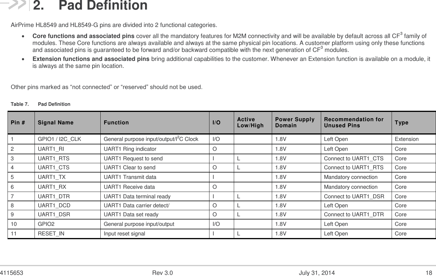
Sierra Wireless HL8549 Module User Manual HL8549 G
Sierra Wireless Inc. Module HL8549 G
UserManual.wiki
>
Sierra Wireless
>
HL8549 User Manual
HL8549-G User manual
Navigation menu
Upload a User Manual
Namespaces
Wiki Guide
HTML
PDF
Info
Views
User Manual
Discussion / Help
Navigation
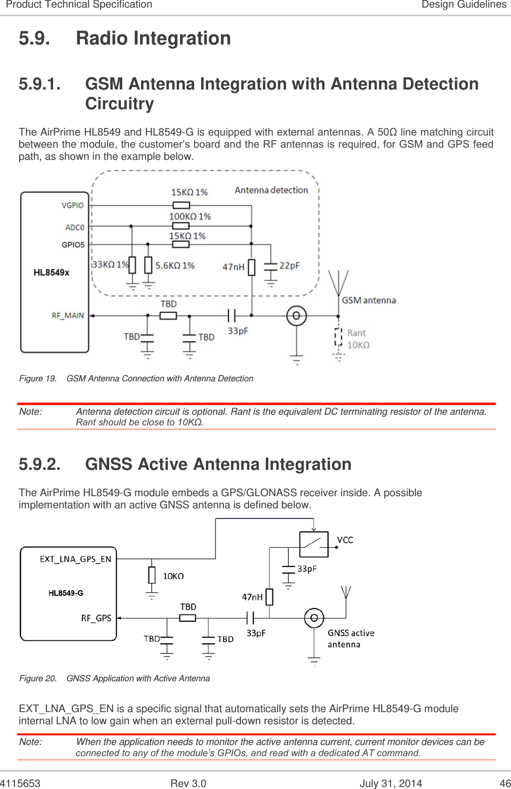
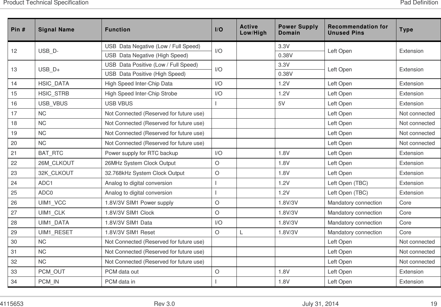
![4115653 Rev 3.0 July 31, 2014 17 Product Technical Specification Introduction Document Current Version Title FCC Part 24E NA Personal Communications Service; Subpart E: Broadband PCS. RSS-132 Issue 2:2005 Cellular telephones employing new technologies operating in the 824-849 MHz and 869-894 MHz bands. RSS-133 Issue 5:2009 2 GHz personal communications services Decree 2338 of 07/10/1997 (ANATEL) 1997 Agência Nacional de Telecomunicações do Brazil. 1.9.3. RoHS Directive Compliant The AirPrime HL8549 and HL8549-G module is compliant with RoHS Directive 2011/65/EU which sets limits for the use of certain restricted hazardous substances. This directive states that “from 1st July 2006, new electrical and electronic equipment put on the market does not contain lead, mercury, cadmium, hexavalent chromium, polybrominated biphenyls (PBB) or polybrominated diphenyl ethers (PBDE)”. 1.9.4. Disposing of the Product This electronic product is subject to the EU Directive 2012/19/EU for Waste Electrical and Electronic Equipment (WEEE). As such, this product must not be disposed of at a municipal waste collection point. Please refer to local regulations for directions on how to dispose of this product in an environmental friendly manner. 1.9.5. References [1] AirPrime HL Series Customer Process Guidelines Reference Number: 4114330 [2] AirPrime HL6 and HL8 Series AT Commands Interface Guide Reference Number: 4114680](https://usermanual.wiki/Sierra-Wireless/HL8549/User-Guide-2497873-Page-17.png)
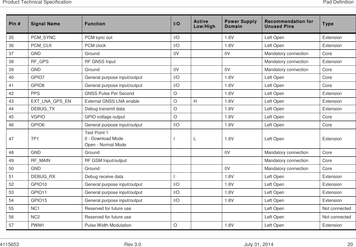
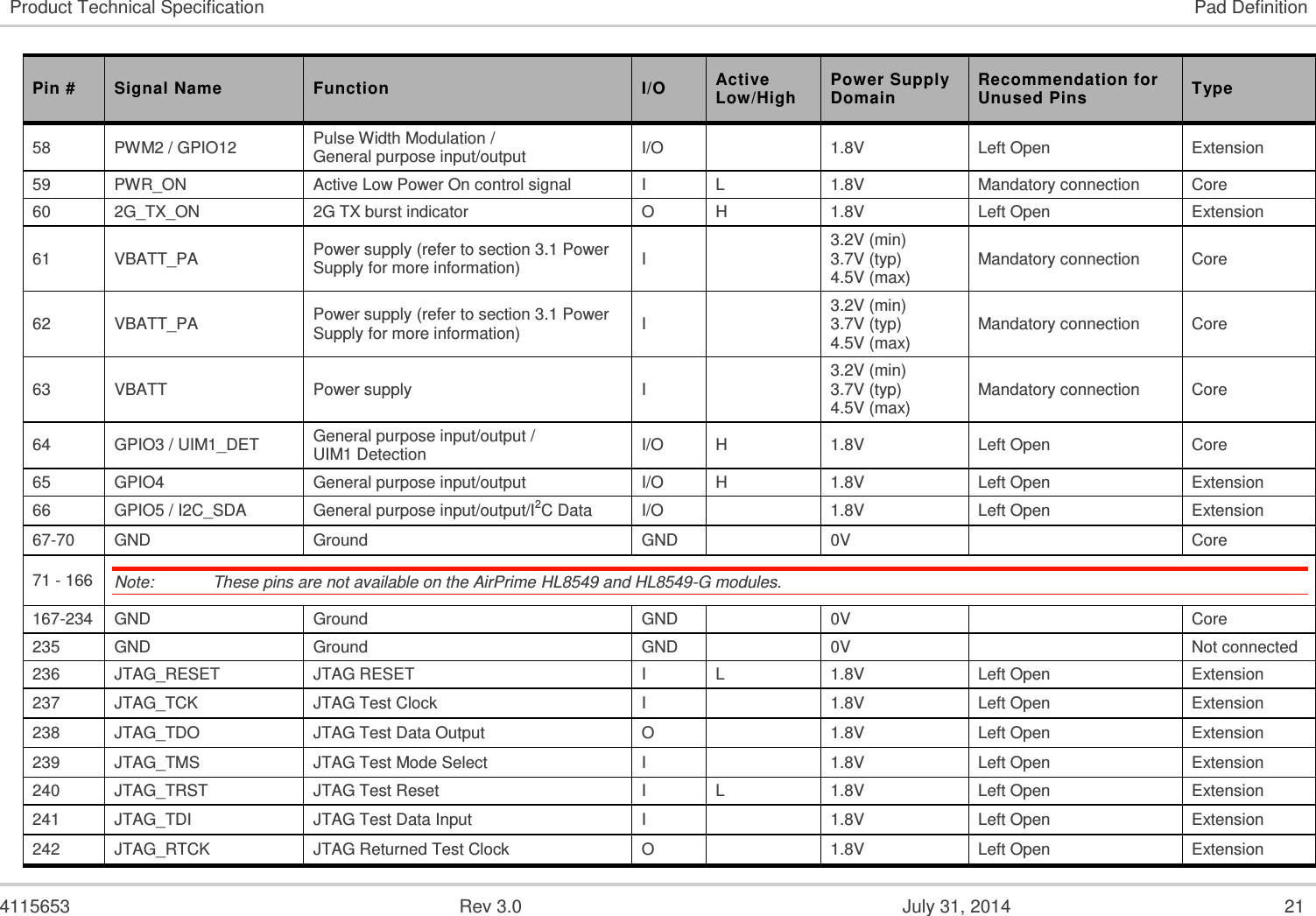
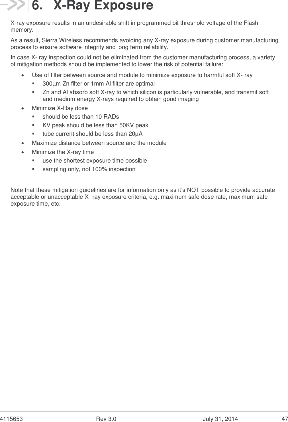
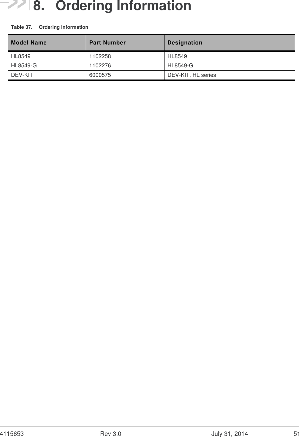
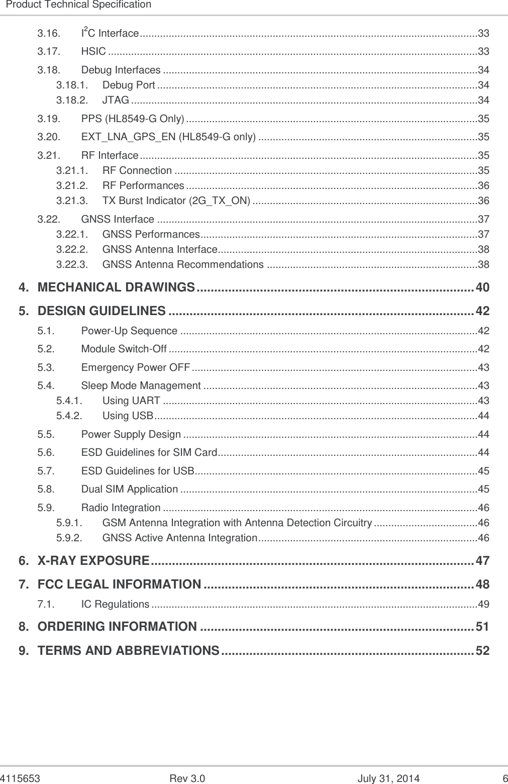
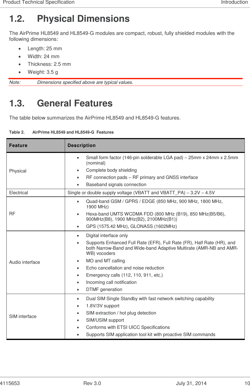
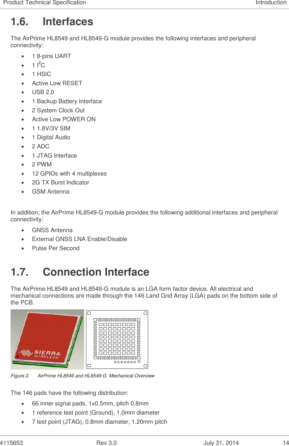
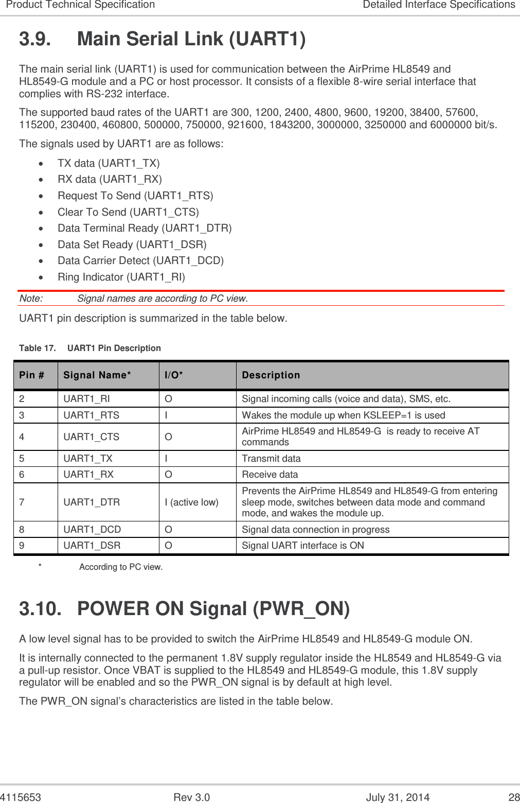
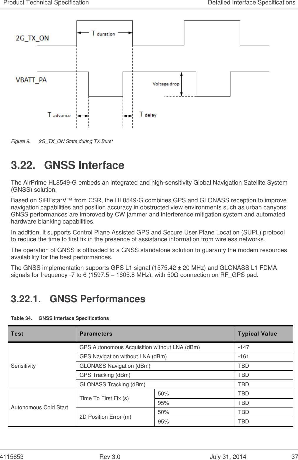
![4115653 Rev 3.0 July 31, 2014 26 Product Technical Specification Detailed Interface Specifications UIM1_RST: reset UIM1_DET: SIM detection Table 13. Electrical Characteristics of UIM1 Parameter Min Typ Max Remarks UIM1 Interface Voltage (V) (VCC,CLK,IO,RST) 2.7 3.0 3.15 The appropriate output voltage is auto detected and selected by software. 1.65 1.80 1.95 UIM1 Detect 1.33 1.80 2.1 High active UIM1_VCC Current (mA) - - 10 Max output current in sleep mode = 3 mA UIM1_VCC Line Regulation (mV/V) - - 50 At Iout_Max UIM1_VCC Power-up Setting Time (µs) from power down - 10 - 3.5.1. UIM1_DET UIM1_DET is used to detect and notify the application about the insertion and removal of a SIM device in the SIM socket connected to the main SIM interface (UIM1). When a SIM is inserted, the state of UIM1_DET transitions from logic 0 to logic 1. Inversely, when a SIM is removed, the state of UIM1_DET transitions from logic 1 to logic 0. Enabling or disabling this SIM detect feature can be done using the AT+KSIMDET command. For more information about this command, refer to document [2] AirPrime HL6 and HL8 Series AT Commands Interface Guide. 3.6. USB The AirPrime HL8549 and HL8549-G have one USB interface. Table 14. USB Pin Description Pin Number Signal Name I/O Function 12 USB_D- I/O USB Data Negative 13 USB_D+ I/O USB Data Positive 16 USB_VBUS I USB VBUS Note: When the 5V USB supply is not available, connect USB_VBUS to VBAT_BB to supply the USB interface. 3.7. Electrical Information for Digital I/O The AirPrime HL8549 and HL8549-G supports three groups of digital interfaces with varying current drain limits. The following list enumerates these interface groupings and Table 15 Digital I/O Electrical Characteristics enumerates the electrical characteristics of each digital interface. Group 1 (8mA current drain limit) UART GPIOs JTAG](https://usermanual.wiki/Sierra-Wireless/HL8549/User-Guide-2497873-Page-26.png)
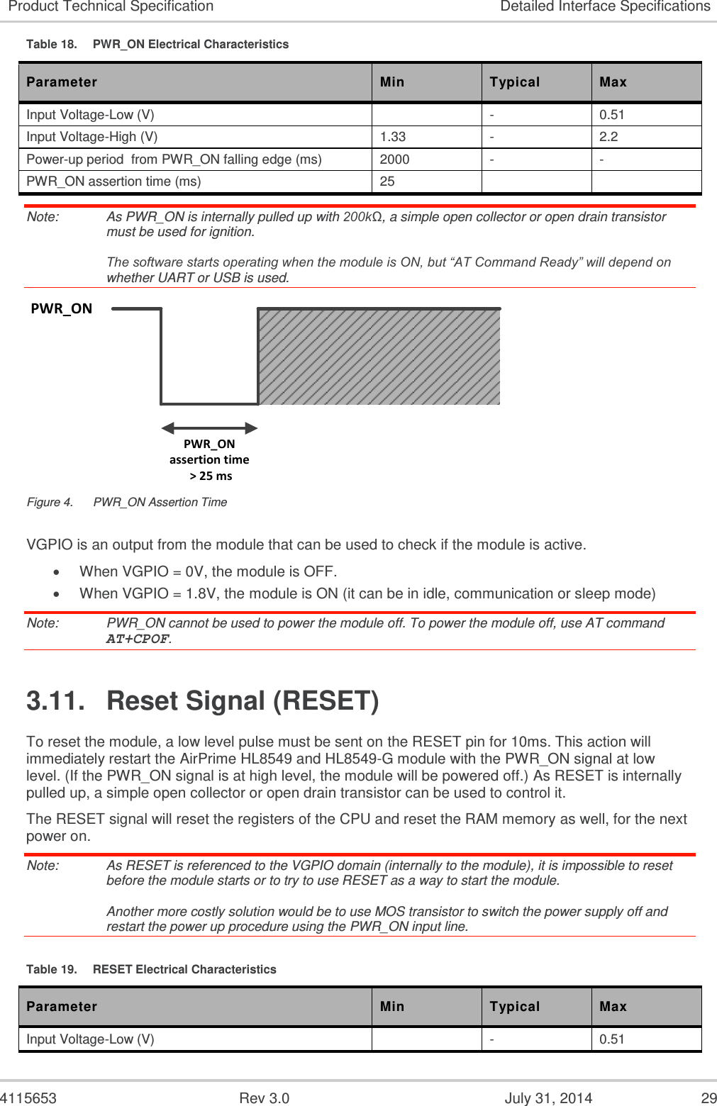
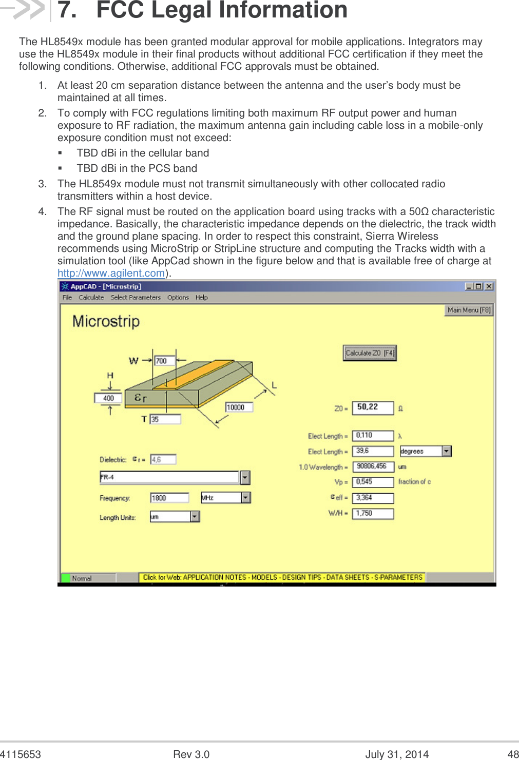
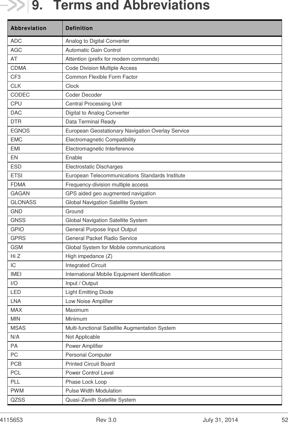
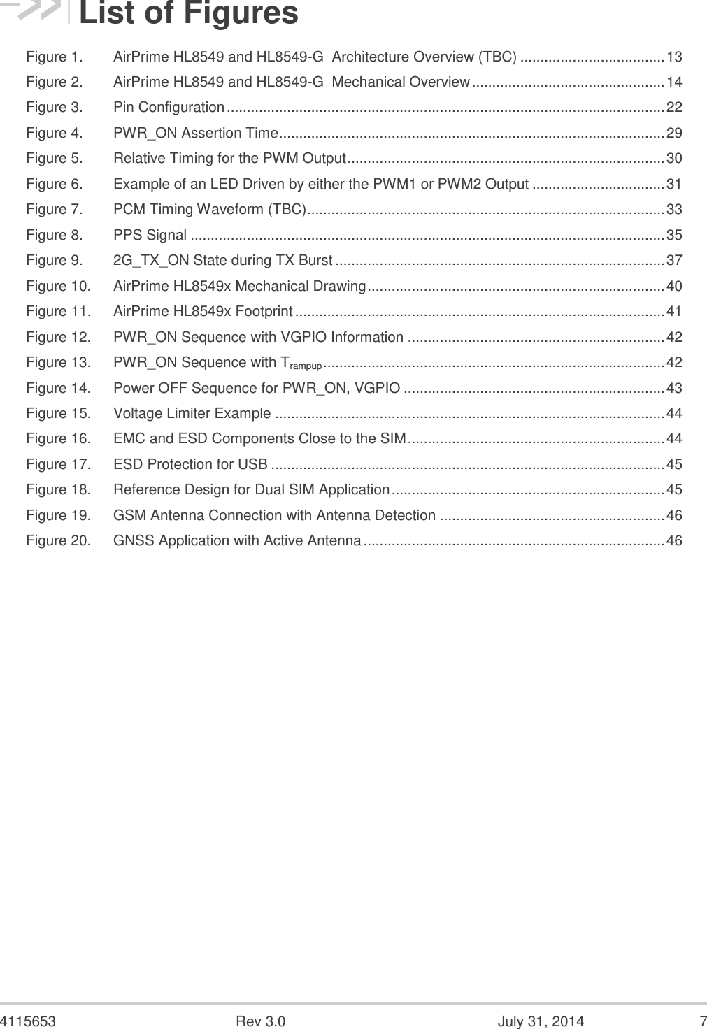
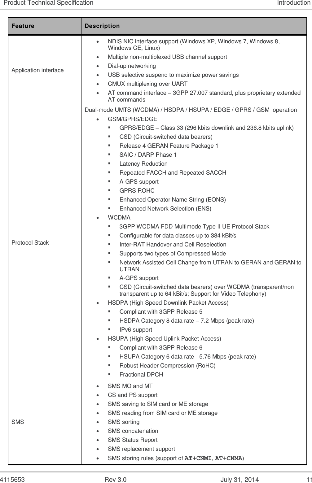
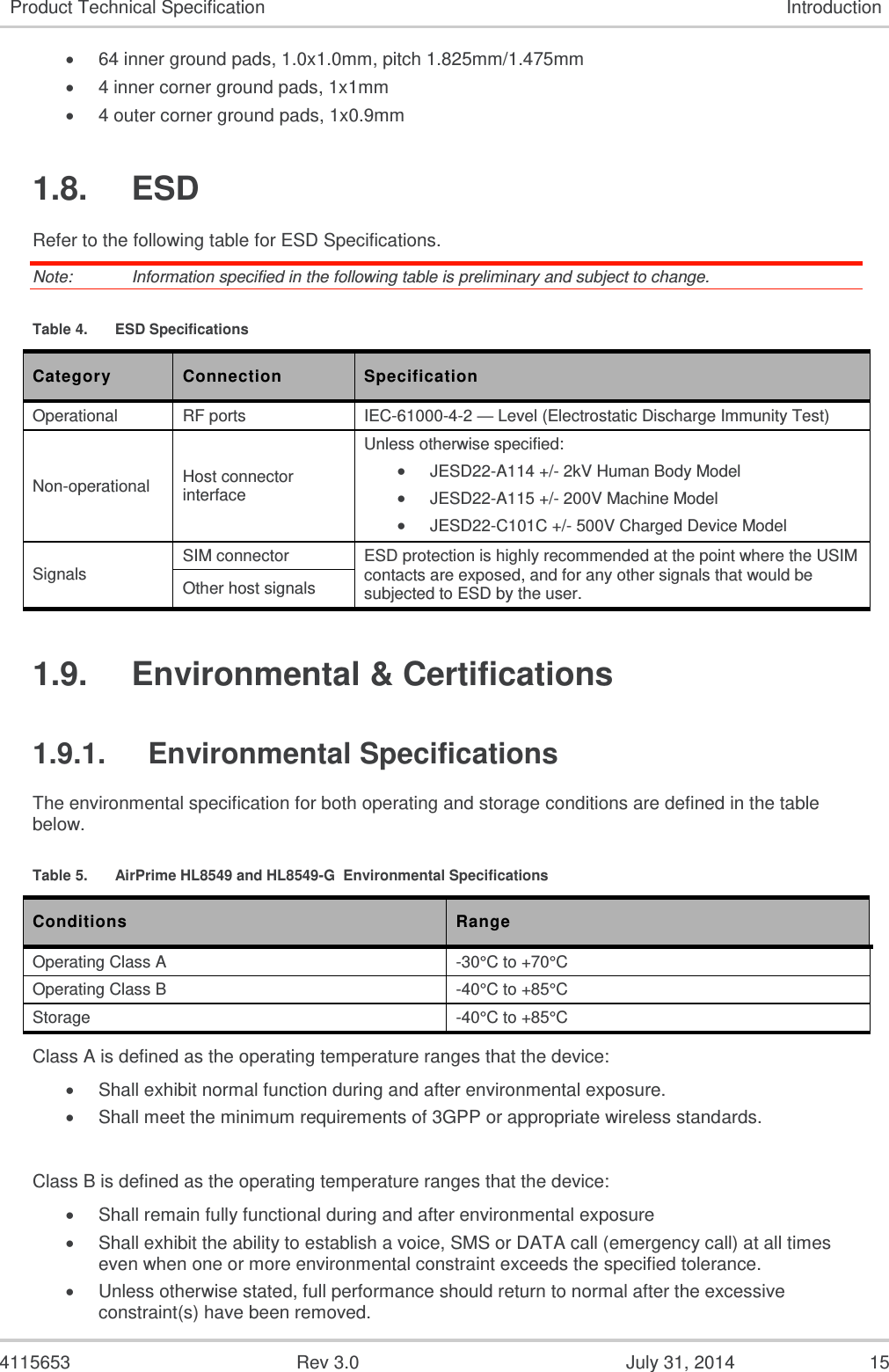
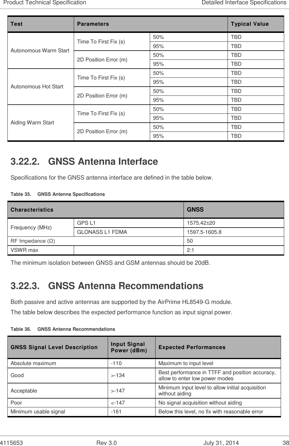
![4115653 Rev 3.0 July 31, 2014 32 Product Technical Specification Detailed Interface Specifications Table 23. Clock Interface Pin Description Pin Number Signal Name I/O I/O Type Description 22 26M_CLKOUT O 1.8V 26MHz Digital Clock output 23 32K_CLKOUT O 1.8V 32.768kHz Digital Clock output Enabling or disabling the clock out feature can be done using AT commands. For more information about AT commands, refer to document [2] AirPrime HL6 and HL8 Series AT Commands Interface Guide. 3.15. PCM The Digital Audio (PCM) Interface allows connectivity with standard audio peripherals. It can be used, for example, to connect an external audio codec. The programmability of this interface allows addressing a large range of audio peripherals. The signals used by the Digital Audio Interface are as follows: PCM_SYNC: The frame synchronization signal delivers an 8 kHz frequency pulse that synchronizes the frame data in and the frame data out. PCM_CLK: The frame bit clock signal controls data transfer with the audio peripheral. PCM_OUT: The frame “data out” relies on the selected configuration mode. PCM_IN: The frame “data in” relies on the selected configuration mode. The PCM interface is a high speed full duplex interface that can be used to send and receive digital audio data to external audio ICs. The Digital Audio Interface also features the following: PCM master or slave 16 bits data word length, linear mode MSB first Configurable PCM bit clock rate on 256kHz, 384kHz or 512kHz Long frame sync Refer to the following table for the electrical characteristics of the digital audio interface. Table 24. Digital Audio Electrical Characteristics Signal Description Minimum Typical Maximum Unit Tsync_low + Tsync_high PCM-SYNC period 125 µs Tsync_low PCM-SYNC low time 124 µs Tsync_high PCM-SYNC high time 1 µs TCLK-cycle PCM-CLK period 3.9 µs TIN-setup PCM-IN setup time 59.6 ns TIN-hold PCM-IN hold time 12 ns TOUT-delay PCM-OUT delay time 21.6 ns TSYNC-delay PCM-SYNC output delay -24 31.2 ns](https://usermanual.wiki/Sierra-Wireless/HL8549/User-Guide-2497873-Page-32.png)
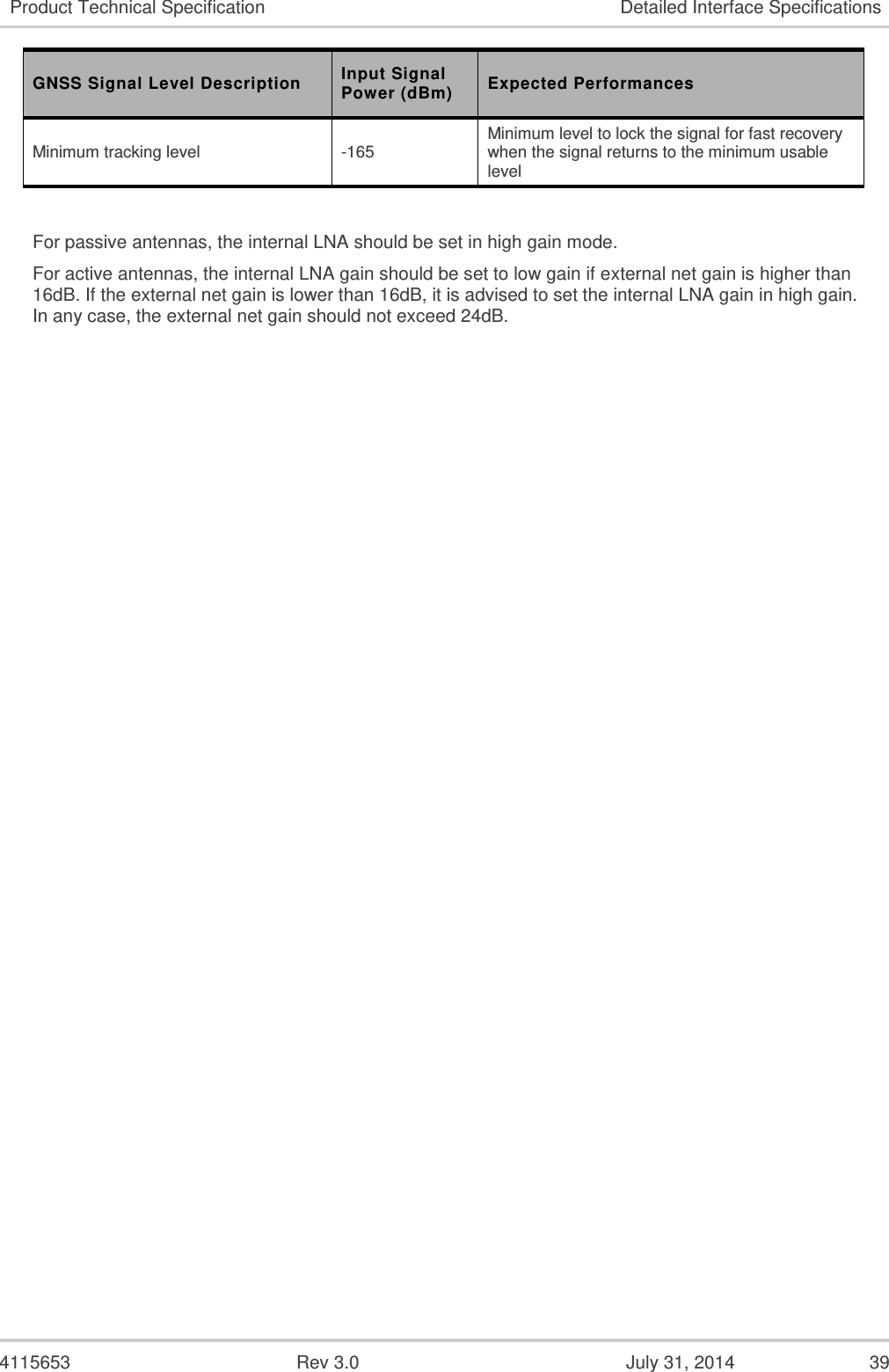
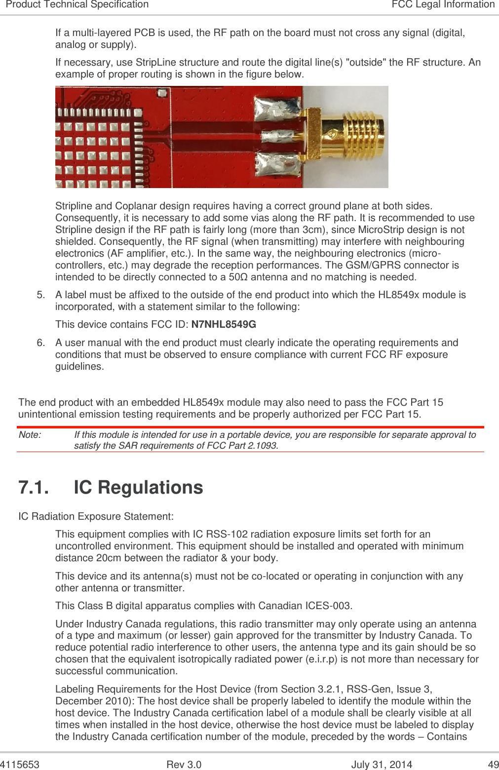
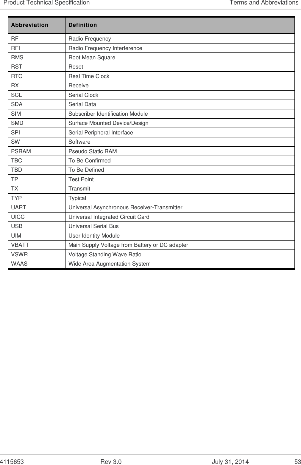
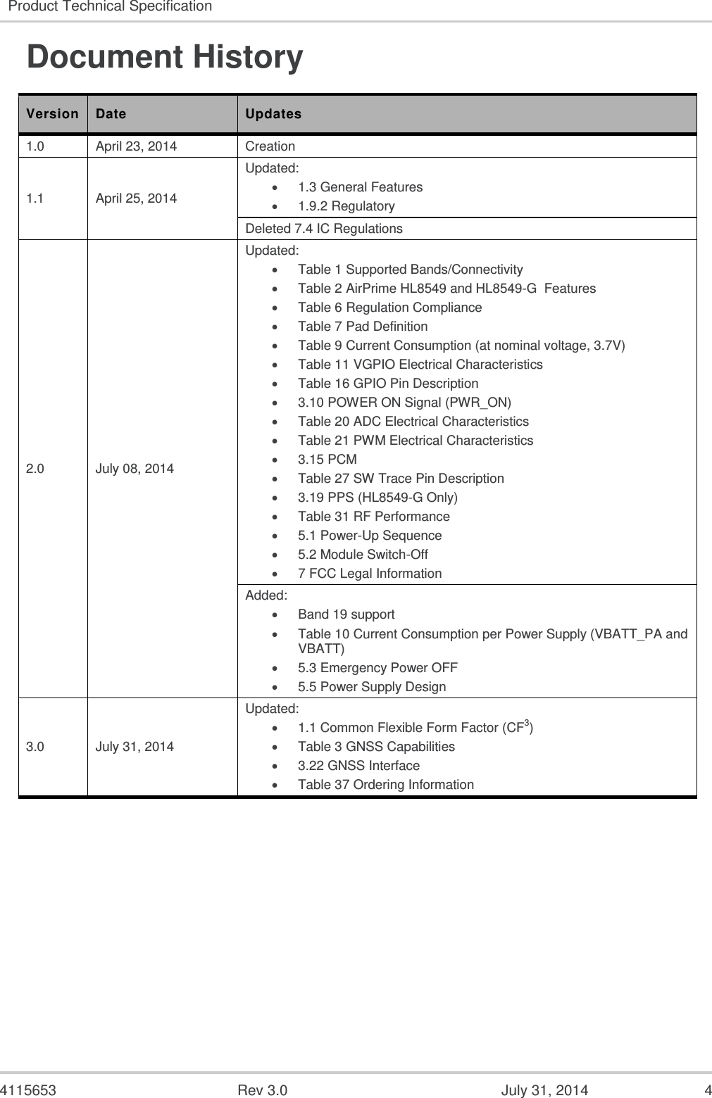
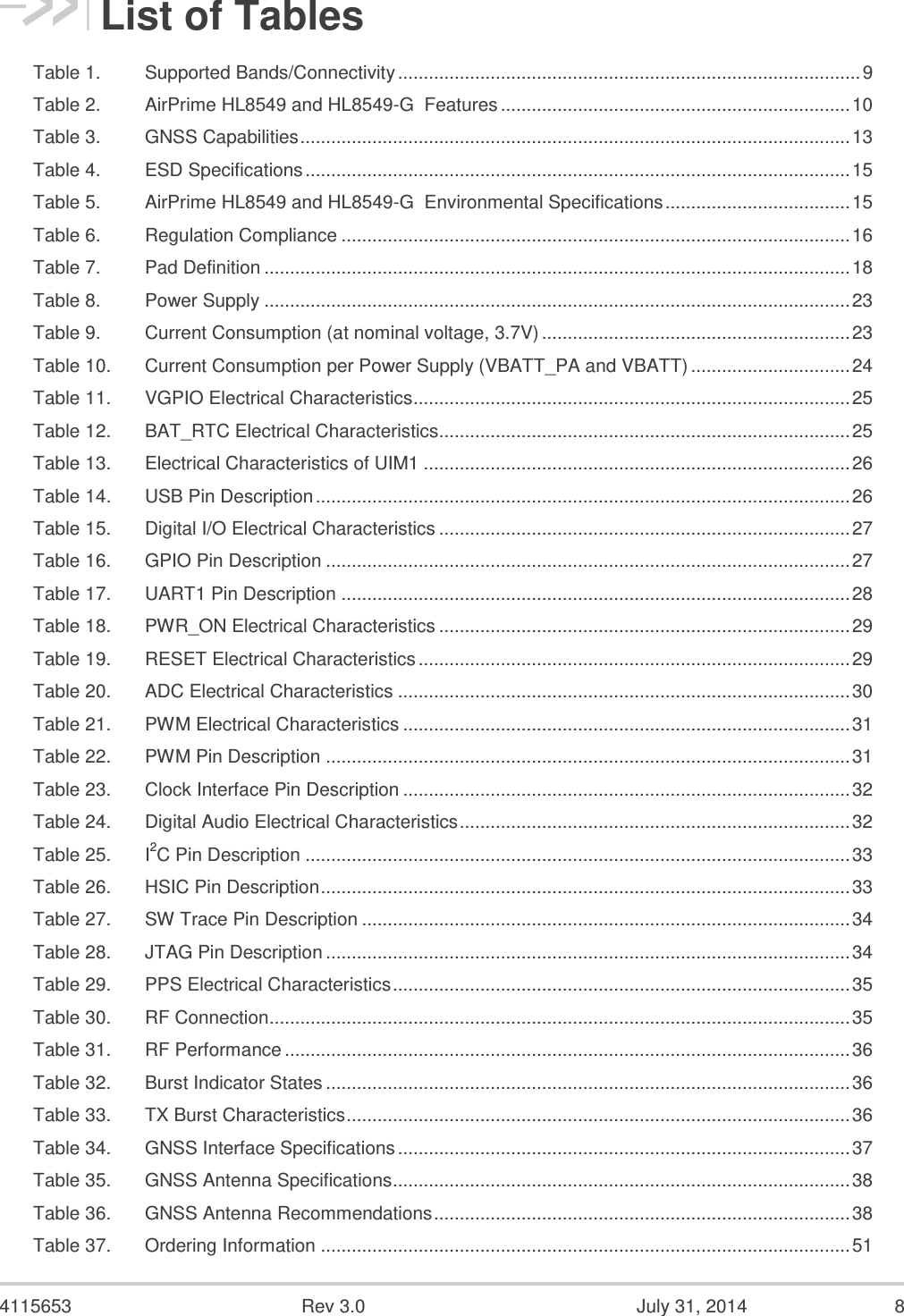
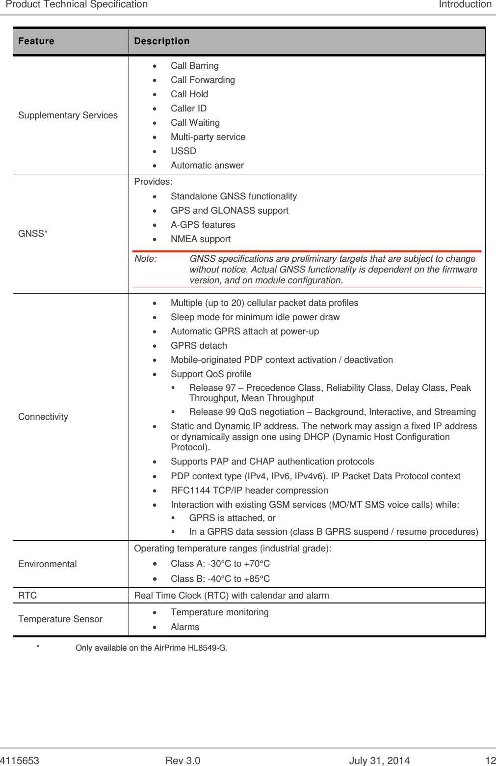
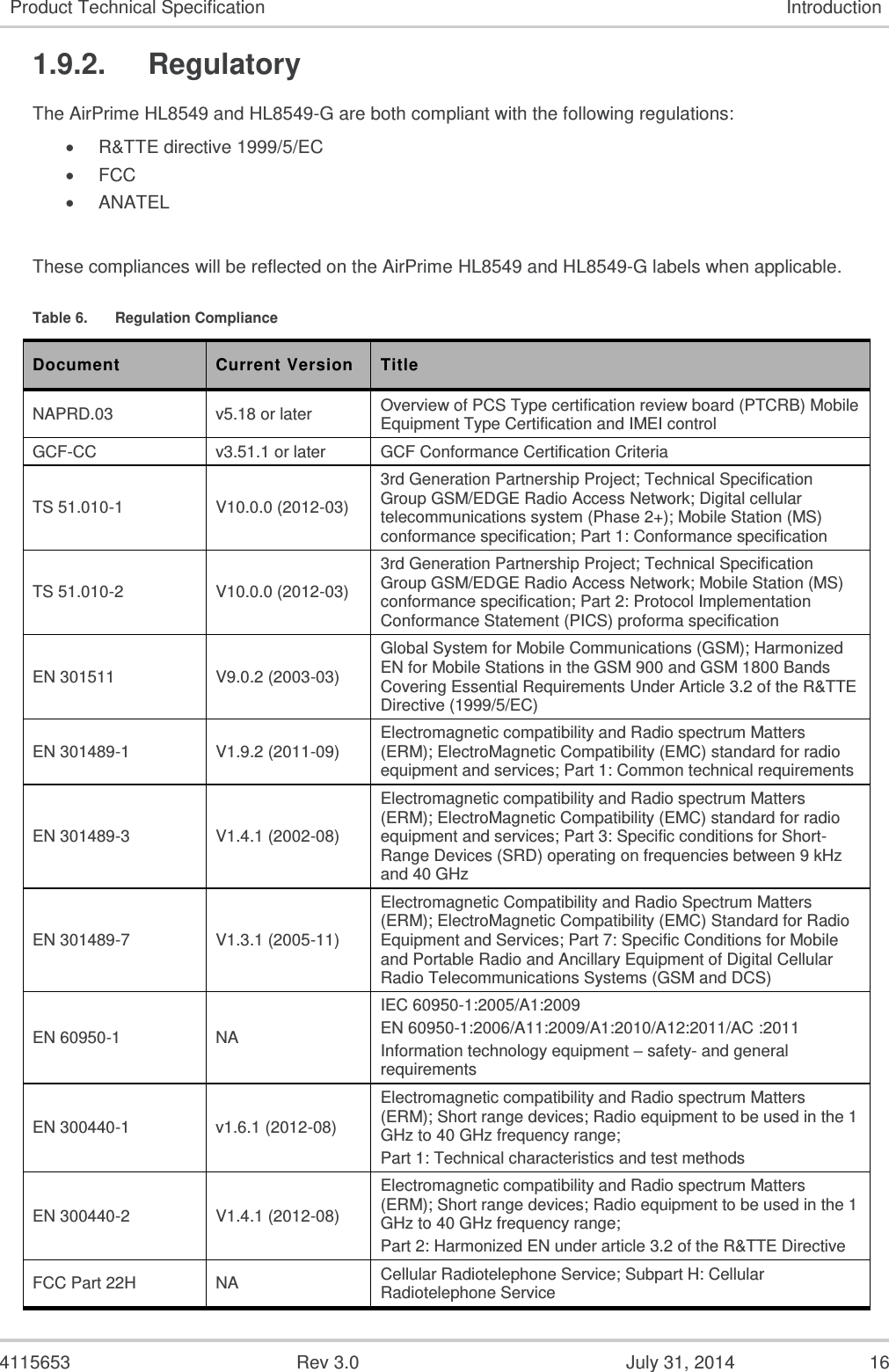
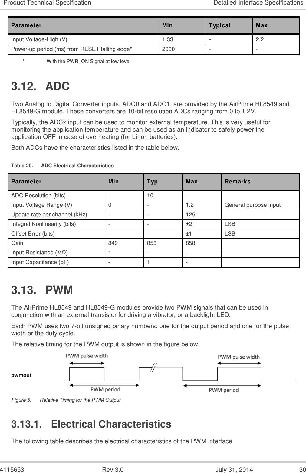
![4115653 Rev 3.0 July 31, 2014 45 Product Technical Specification Design Guidelines 5.7. ESD Guidelines for USB When the USB interface is externally accessible, it is required to have ESD protection on the USB_VBUS, USB_D+ and USB_D- signals. Figure 17. ESD Protection for USB Note: It is not recommended to have an ESD diode with feedback path from USB_VBUS to either USB_D+ or USB_D-. 5.8. Dual SIM Application Using an external switch and GPIOs, the HL8549 and HL8549-G can support Dual SIM Single Standby with fast network switching. Refer to document [2] AirPrime HL6 and HL8 Series AT Commands Interface Guide for related AT commands. Figure 18. Reference Design for Dual SIM Application](https://usermanual.wiki/Sierra-Wireless/HL8549/User-Guide-2497873-Page-45.png)