Sierra Wireless MC7475 Radio Module User Manual AirPrime MC7475 Product Technical Specification
Sierra Wireless Inc. Radio Module AirPrime MC7475 Product Technical Specification
Contents
- 1. MC7475 User Manual
- 2. MC7475 User Manual_r3
MC7475 User Manual_r3
AirPrime MC7475
Product Technical Specification
41110251
Rev 3
Proprietary and Confidential
Contents subject to change

Product Technical Specification
Rev 3 Sep.17 2 41110251
Important
Notice
Due to the nature of wireless communications, transmission and reception of data
can never be guaranteed. Data may be delayed, corrupted (i.e., have errors) or be
totally lost. Although significant delays or losses of data are rare when wireless
devices such as the Sierra Wireless modem are used in a normal manner with a
well-constructed network, the Sierra Wireless modem should not be used in
situations where failure to transmit or receive data could result in damage of any
kind to the user or any other party, including but not limited to personal injury,
death, or loss of property. Sierra Wireless accepts no responsibility for damages
of any kind resulting from delays or errors in data transmitted or received using
the Sierra Wireless modem, or for failure of the Sierra Wireless modem to
transmit or receive such data.
Safety and
Hazards
Do not operate the Sierra Wireless modem in areas where blasting is in progress,
where explosive atmospheres may be present, near medical equipment, near life
support equipment, or any equipment which may be susceptible to any form of
radio interference. In such areas, the Sierra Wireless modem MUST BE
POWERED OFF. The Sierra Wireless modem can transmit signals that could
interfere with this equipment.
Do not operate the Sierra Wireless modem in any aircraft, whether the aircraft is
on the ground or in flight. In aircraft, the Sierra Wireless modem MUST BE
POWERED OFF. When operating, the Sierra Wireless modem can transmit
signals that could interfere with various onboard systems.
Note: Some airlines may permit the use of cellular phones while the aircraft is on the
ground and the door is open. Sierra Wireless modems may be used at this time.
The driver or operator of any vehicle should not operate the Sierra Wireless
modem while in control of a vehicle. Doing so will detract from the driver or
operator's control and operation of that vehicle. In some states and provinces,
operating such communications devices while in control of a vehicle is an offence.
Limitation of
Liability
The information in this manual is subject to change without notice and does not
represent a commitment on the part of Sierra Wireless. SIERRA WIRELESS AND
ITS AFFILIATES SPECIFICALLY DISCLAIM LIABILITY FOR ANY AND ALL
DIRECT, INDIRECT, SPECIAL, GENERAL, INCIDENTAL, CONSEQUENTIAL,
PUNITIVE OR EXEMPLARY DAMAGES INCLUDING, BUT NOT LIMITED TO,
LOSS OF PROFITS OR REVENUE OR ANTICIPATED PROFITS OR REVENUE
ARISING OUT OF THE USE OR INABILITY TO USE ANY SIERRA WIRELESS
PRODUCT, EVEN IF SIERRA WIRELESS AND/OR ITS AFFILIATES HAS BEEN
ADVISED OF THE POSSIBILITY OF SUCH DAMAGES OR THEY ARE
FORESEEABLE OR FOR CLAIMS BY ANY THIRD PARTY.
Notwithstanding the foregoing, in no event shall Sierra Wireless and/or its
affiliates aggregate liability arising under or in connection with the Sierra Wireless
product, regardless of the number of events, occurrences, or claims giving rise to
liability, be in excess of the price paid by the purchaser for the Sierra Wireless
product.
Preface
Rev 3 Sep.17 3 41110251
Copyright ©2017 Sierra Wireless. All rights reserved.
Trademarks Sierra Wireless®, AirPrime®, AirLink®, AirVantage® and the Sierra Wireless logo
are registered trademarks of Sierra Wireless, Inc.
Windows® and Windows Vista® are registered trademarks of Microsoft
Corporation.
Other trademarks are the property of their respective owners.
Contact
Information
Revision
History
Sales information and technical
support, including warranty and returns Web: sierrawireless.com/company/contact-us/
Global toll-free number: 1-877-687-7795
6:00 am to 5:00 pm PST
Corporate and product information Web: sierrawireless.com
Revision
number Release date Changes
1June 2017 Initial release
2June 2017 Updated Miscellaneous DC Power Consumption table:
·Updated notes, corrected module number typo
3September 2017 Updated Regulatory section (antenna gain, EIRP limit, FCC ID, FCC Part 27 notice)
Updated GPS Specifications—Acquisition times
Updated module dimensions
Updated dimensioned view figure
Updated sample label
Updated Copper Pad Location figure

Rev 3 Sep.17 4 41110251
Contents
Introduction . . . . . . . . . . . . . . . . . . . . . . . . . . . . . . . . . . . . . . . . . . . . . . . . . . . . . . . . . . . . .9
Supported RF Bands . . . . . . . . . . . . . . . . . . . . . . . . . . . . . . . . . . . . . . . . . . . . . . . . . . . 9
Physical Features. . . . . . . . . . . . . . . . . . . . . . . . . . . . . . . . . . . . . . . . . . . . . . . . . . . . . . 9
Application Interface Features . . . . . . . . . . . . . . . . . . . . . . . . . . . . . . . . . . . . . . . . . . . . 9
Modem Features . . . . . . . . . . . . . . . . . . . . . . . . . . . . . . . . . . . . . . . . . . . . . . . . . . . . . 10
LTE Features . . . . . . . . . . . . . . . . . . . . . . . . . . . . . . . . . . . . . . . . . . . . . . . . . . . . . . . . 10
Position Location (GPS) . . . . . . . . . . . . . . . . . . . . . . . . . . . . . . . . . . . . . . . . . . . . . . . . 10
Supporting Documents. . . . . . . . . . . . . . . . . . . . . . . . . . . . . . . . . . . . . . . . . . . . . . . . . 10
Required Connectors . . . . . . . . . . . . . . . . . . . . . . . . . . . . . . . . . . . . . . . . . . . . . . . . . . 11
Ordering Information. . . . . . . . . . . . . . . . . . . . . . . . . . . . . . . . . . . . . . . . . . . . . . . . . . . 11
Integration Requirements . . . . . . . . . . . . . . . . . . . . . . . . . . . . . . . . . . . . . . . . . . . . . . . 11
Standards Compliance . . . . . . . . . . . . . . . . . . . . . . . . . . . . . . . . . . . . . . . . . . . . . . . . . . .12
Electrical Specifications . . . . . . . . . . . . . . . . . . . . . . . . . . . . . . . . . . . . . . . . . . . . . . . . . .13
Host Interface Pin Assignments . . . . . . . . . . . . . . . . . . . . . . . . . . . . . . . . . . . . . . . . . . 14
Power Supply . . . . . . . . . . . . . . . . . . . . . . . . . . . . . . . . . . . . . . . . . . . . . . . . . . . . . . . . 18
USB Interface . . . . . . . . . . . . . . . . . . . . . . . . . . . . . . . . . . . . . . . . . . . . . . . . . . . . . . . . 18
USB Throughput Performance . . . . . . . . . . . . . . . . . . . . . . . . . . . . . . . . . . . . . . . . .18
SIM Interface . . . . . . . . . . . . . . . . . . . . . . . . . . . . . . . . . . . . . . . . . . . . . . . . . . . . . . . . 19
SIM Implementation . . . . . . . . . . . . . . . . . . . . . . . . . . . . . . . . . . . . . . . . . . . . . . . . .21
Control Interface (Signals) . . . . . . . . . . . . . . . . . . . . . . . . . . . . . . . . . . . . . . . . . . . . . . 22
WAKE_N — Wake Host . . . . . . . . . . . . . . . . . . . . . . . . . . . . . . . . . . . . . . . . . . . . . .22
WAN_LED_N—LED Output . . . . . . . . . . . . . . . . . . . . . . . . . . . . . . . . . . . . . . . . . .22
SYSTEM_RESET_N—Reset Input . . . . . . . . . . . . . . . . . . . . . . . . . . . . . . . . . . . . .23
Antenna Control . . . . . . . . . . . . . . . . . . . . . . . . . . . . . . . . . . . . . . . . . . . . . . . . . . . . . . 23
RF Specifications . . . . . . . . . . . . . . . . . . . . . . . . . . . . . . . . . . . . . . . . . . . . . . . . . . . . . . .24
RF Connections . . . . . . . . . . . . . . . . . . . . . . . . . . . . . . . . . . . . . . . . . . . . . . . . . . . . . . 24
Shielding . . . . . . . . . . . . . . . . . . . . . . . . . . . . . . . . . . . . . . . . . . . . . . . . . . . . . . . . .24
Antenna and Cabling . . . . . . . . . . . . . . . . . . . . . . . . . . . . . . . . . . . . . . . . . . . . . . . .25
Ground Connection . . . . . . . . . . . . . . . . . . . . . . . . . . . . . . . . . . . . . . . . . . . . . . . . . . . 25

Contents
Rev 3 Sep.17 5 41110251
Interference and Sensitivity . . . . . . . . . . . . . . . . . . . . . . . . . . . . . . . . . . . . . . . . . . . . . 26
Interference From Other Wireless Devices . . . . . . . . . . . . . . . . . . . . . . . . . . . . . . . 26
Host-generated RF Interference . . . . . . . . . . . . . . . . . . . . . . . . . . . . . . . . . . . . . . . 26
Device-generated RF Interference . . . . . . . . . . . . . . . . . . . . . . . . . . . . . . . . . . . . . 26
Methods to Mitigate Decreased Rx Performance . . . . . . . . . . . . . . . . . . . . . . . . . . 27
Radiated Spurious Emissions (RSE) . . . . . . . . . . . . . . . . . . . . . . . . . . . . . . . . . . . . 27
Radiated Sensitivity Measurement . . . . . . . . . . . . . . . . . . . . . . . . . . . . . . . . . . . . . . . 27
Sierra Wireless’ Sensitivity Testing and Desensitization Investigation . . . . . . . . . . 27
Sensitivity vs. Frequency . . . . . . . . . . . . . . . . . . . . . . . . . . . . . . . . . . . . . . . . . . . . . 28
Supported Frequencies . . . . . . . . . . . . . . . . . . . . . . . . . . . . . . . . . . . . . . . . . . . . . . . . 28
Conducted Rx Sensitivity / Tx Power. . . . . . . . . . . . . . . . . . . . . . . . . . . . . . . . . . . . . . 28
GPS Specifications . . . . . . . . . . . . . . . . . . . . . . . . . . . . . . . . . . . . . . . . . . . . . . . . . . . 29
Power . . . . . . . . . . . . . . . . . . . . . . . . . . . . . . . . . . . . . . . . . . . . . . . . . . . . . . . . . . . . . . . . . 30
Power Consumption. . . . . . . . . . . . . . . . . . . . . . . . . . . . . . . . . . . . . . . . . . . . . . . . . . . 30
Power Interface . . . . . . . . . . . . . . . . . . . . . . . . . . . . . . . . . . . . . . . . . . . . . . . . . . . . . . 31
Power Ramp-up . . . . . . . . . . . . . . . . . . . . . . . . . . . . . . . . . . . . . . . . . . . . . . . . . . . . 31
Power-On/Off Timing . . . . . . . . . . . . . . . . . . . . . . . . . . . . . . . . . . . . . . . . . . . . . . . 31
Power Supply Noise . . . . . . . . . . . . . . . . . . . . . . . . . . . . . . . . . . . . . . . . . . . . . . . . 33
Mechanical and Environmental Specifications . . . . . . . . . . . . . . . . . . . . . . . . . . . . . . . 34
Device Views . . . . . . . . . . . . . . . . . . . . . . . . . . . . . . . . . . . . . . . . . . . . . . . . . . . . . . . . 35
Labeling . . . . . . . . . . . . . . . . . . . . . . . . . . . . . . . . . . . . . . . . . . . . . . . . . . . . . . . . . . . . 36
Electrostatic Discharge (ESD) . . . . . . . . . . . . . . . . . . . . . . . . . . . . . . . . . . . . . . . . . 36
Thermal Considerations. . . . . . . . . . . . . . . . . . . . . . . . . . . . . . . . . . . . . . . . . . . . . . . . 37
Regulatory Compliance and Industry Certifications . . . . . . . . . . . . . . . . . . . . . . . . . . . 40
Important Notice. . . . . . . . . . . . . . . . . . . . . . . . . . . . . . . . . . . . . . . . . . . . . . . . . . . . . . 40
Safety and Hazards . . . . . . . . . . . . . . . . . . . . . . . . . . . . . . . . . . . . . . . . . . . . . . . . . . . 40
Important Compliance Information for the United States of America. . . . . . . . . . . . . . 41
Antenna Specification . . . . . . . . . . . . . . . . . . . . . . . . . . . . . . . . . . . . . . . . . . . . . . . . . . . 43
Recommended Main/Rx Diversity Antenna Specifications . . . . . . . . . . . . . . . . . . . . . 43

Product Technical Specification
Rev 3 Sep.17 6 41110251
Recommended GPS Antenna Specifications . . . . . . . . . . . . . . . . . . . . . . . . . . . . . . . 45
Antenna Tests . . . . . . . . . . . . . . . . . . . . . . . . . . . . . . . . . . . . . . . . . . . . . . . . . . . . . . . 45
Design Checklist . . . . . . . . . . . . . . . . . . . . . . . . . . . . . . . . . . . . . . . . . . . . . . . . . . . . . . . 47
Packaging . . . . . . . . . . . . . . . . . . . . . . . . . . . . . . . . . . . . . . . . . . . . . . . . . . . . . . . . . . . . . 49
References . . . . . . . . . . . . . . . . . . . . . . . . . . . . . . . . . . . . . . . . . . . . . . . . . . . . . . . . . . . . 51
Sierra Wireless Documents . . . . . . . . . . . . . . . . . . . . . . . . . . . . . . . . . . . . . . . . . . . . . 51
Command Documents . . . . . . . . . . . . . . . . . . . . . . . . . . . . . . . . . . . . . . . . . . . . . . . 51
Industry/Other Documents . . . . . . . . . . . . . . . . . . . . . . . . . . . . . . . . . . . . . . . . . . . 51
Acronyms . . . . . . . . . . . . . . . . . . . . . . . . . . . . . . . . . . . . . . . . . . . . . . . . . . . . . . . . . . . . . 52
Index. . . . . . . . . . . . . . . . . . . . . . . . . . . . . . . . . . . . . . . . . . . . . . . . . . . . . . . . . . . . . . . . . 57

Rev 3 Sep.17 7 41110251
List of Tables
Table 1-1: Supported RF Bands . . . . . . . . . . . . . . . . . . . . . . . . . . . . . . . . . . . . . . . . . . . . . 9
Table 1-2: Required Host-Module Connectors . . . . . . . . . . . . . . . . . . . . . . . . . . . . . . . . . 11
Table 2-1: Standards Compliance . . . . . . . . . . . . . . . . . . . . . . . . . . . . . . . . . . . . . . . . . . . 12
Table 3-1: Connector Pin Assignments . . . . . . . . . . . . . . . . . . . . . . . . . . . . . . . . . . . . . . . 14
Table 3-2: Power and Ground Specifications . . . . . . . . . . . . . . . . . . . . . . . . . . . . . . . . . . 18
Table 3-3: USB Interfaces . . . . . . . . . . . . . . . . . . . . . . . . . . . . . . . . . . . . . . . . . . . . . . . . . 18
Table 3-4: SIM Interface Signals . . . . . . . . . . . . . . . . . . . . . . . . . . . . . . . . . . . . . . . . . . . . 19
Table 3-5: Module Control Signals. . . . . . . . . . . . . . . . . . . . . . . . . . . . . . . . . . . . . . . . . . . 22
Table 3-6: Antenna Control Signals. . . . . . . . . . . . . . . . . . . . . . . . . . . . . . . . . . . . . . . . . . 23
Table 4-1: LTE Frequency Bands . . . . . . . . . . . . . . . . . . . . . . . . . . . . . . . . . . . . . . . . . . . 28
Table 4-2: Conducted Rx (Receive) Sensitivity—LTE Bands . . . . . . . . . . . . . . . . . . . . . . 28
Table 4-3: Conducted Tx (Transmit) Power Tolerances . . . . . . . . . . . . . . . . . . . . . . . . . . 28
Table 4-4: GPS Specifications. . . . . . . . . . . . . . . . . . . . . . . . . . . . . . . . . . . . . . . . . . . . . . 29
Table 5-1: Averaged Standby DC Power Consumption. . . . . . . . . . . . . . . . . . . . . . . . . . . 30
Table 5-2: Averaged Call Mode DC Power Consumption . . . . . . . . . . . . . . . . . . . . . . . . . 31
Table 5-3: Miscellaneous DC Power Consumption . . . . . . . . . . . . . . . . . . . . . . . . . . . . . . 31
Table 5-4: USB 2.0 Power-On/Off Timing Parameters (Double Enumeration) . . . . . . . . . 32
Table 5-5: USB 2.0 Power-On/Off Timing Parameters (Single Enumeration) . . . . . . . . . . 32
Table 6-1: Mechanical and Environmental Specifications . . . . . . . . . . . . . . . . . . . . . . . . . 34
Table 7-1: Antenna Gain Specifications. . . . . . . . . . . . . . . . . . . . . . . . . . . . . . . . . . . . . . . 41
Table 7-2: Collocated Radio Transmitter Specifications . . . . . . . . . . . . . . . . . . . . . . . . . . 42
Table 8-1: Antenna Requirements . . . . . . . . . . . . . . . . . . . . . . . . . . . . . . . . . . . . . . . . . . 43
Table 8-2: GPS Antenna Requirements . . . . . . . . . . . . . . . . . . . . . . . . . . . . . . . . . . . . . . 45
Table 9-1: Hardware Integration Design Considerations. . . . . . . . . . . . . . . . . . . . . . . . . . 47
Table A-1: Acronyms and Definitions. . . . . . . . . . . . . . . . . . . . . . . . . . . . . . . . . . . . . . . . . 52

Rev 3 Sep.17 8 41110251
List of Figures
Figure 3-1: System Block Diagram . . . . . . . . . . . . . . . . . . . . . . . . . . . . . . . . . . . . . . . . . . 13
Figure 3-2: SIM Application Interface (applies to both SIM interfaces) . . . . . . . . . . . . . . . 20
Figure 3-3: SIM Card Contacts (Contact View) . . . . . . . . . . . . . . . . . . . . . . . . . . . . . . . . . 20
Figure 3-4: Recommended WAKE_N Connection. . . . . . . . . . . . . . . . . . . . . . . . . . . . . . . 22
Figure 3-5: Example LED. . . . . . . . . . . . . . . . . . . . . . . . . . . . . . . . . . . . . . . . . . . . . . . . . . 23
Figure 4-1: Module Connectors . . . . . . . . . . . . . . . . . . . . . . . . . . . . . . . . . . . . . . . . . . . . . 24
Figure 5-1: Signal Timing (USB Enumeration). . . . . . . . . . . . . . . . . . . . . . . . . . . . . . . . . . 32
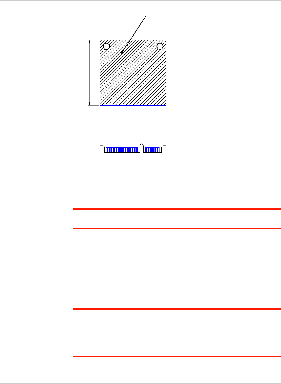
Figure 6-1: Top View . . . . . . . . . . . . . . . . . . . . . . . . . . . . . . . . . . . . . . . . . . . . . . . . . . . . . 35
Figure 6-2: Dimensioned View. . . . . . . . . . . . . . . . . . . . . . . . . . . . . . . . . . . . . . . . . . . . . . 35
Figure 6-3: Sample Unit Label . . . . . . . . . . . . . . . . . . . . . . . . . . . . . . . . . . . . . . . . . . . . . . 36
Figure 6-4: Shield locations (Top view) . . . . . . . . . . . . . . . . . . . . . . . . . . . . . . . . . . . . . . . 37
Figure 6-5: Copper Pad Location on Bottom Side of Module . . . . . . . . . . . . . . . . . . . . . . 38
Figure 10-1: Device Placement in Module Tray. . . . . . . . . . . . . . . . . . . . . . . . . . . . . . . . . 49
Figure 10-2: Shipping Package . . . . . . . . . . . . . . . . . . . . . . . . . . . . . . . . . . . . . . . . . . . . . 50
Figure 10-3: Outer (shipping) Box . . . . . . . . . . . . . . . . . . . . . . . . . . . . . . . . . . . . . . . . . . . 50
Rev 3 Sep.17 9 41110251
1
1: Introduction
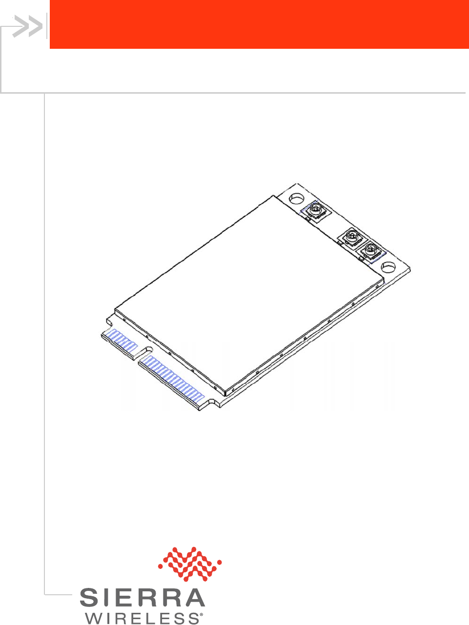
The Sierra Wireless MC7475 PCI Express Mini Card is a compact, lightweight,
wireless modem that provides LTE and GPS connectivity for M2M applications,
notebook, ultrabook and tablet computers over several radio frequency bands.
Supported RF Bands
The modem, based on the Altair FourGee6300 baseband processor, supports data
operation on LTE networks over the bands described in Table 1-1.
Physical Features
•Small form factor—conforms to type F2 as specified in PCI Express Mini Card
Electromechanical Specification Revision 1.2.
•Ambient operating temperature range:
·Class A (3GPP compliant): -20°C to +70°C
·Class B (operational, non-3GPP compliant): -30°C to +85°C (reduced
operating parameters required)
Important: The internal module temperature must be kept below 90°C. For best perfor-
mance, the internal module temperature should be kept below 80°C. Proper mounting, heat
sinks, and active cooling may be required, depending on the integrated application.
Application Interface Features
•USB interface
•AT command interface
•Support for active antenna control via dedicated antenna control signals
(ANT_CTRL0:3)
•Dynamic power reduction support via software and dedicated signal (DPR)
Table 1-1: Supported RF Bands
Technology Bands Notes
LTE 2, 4, 12, 125 Data rates:
•Downlink (Cat 4):
FDD: 150 Mbps
•Uplink (Cat 4):
FDD: 50 Mbps
GPS 1575.42 MHz

Product Technical Specification
Rev 3 Sep.17 10 41110251
Modem Features
•Traditional modem COM port support for AT commands
•USB suspend / resume
•Sleep mode for minimum idle power draw
•Enhanced Operator Name String (EONS)
•Mobile-originated PDP context activation / deactivation
•Static and Dynamic IP address. The network may assign a fixed IP address
or dynamically assign one using DHCP (Dynamic Host Configuration
Protocol).
•PAP and CHAP support
•PDP context type (IPv4, IPv6, or IPv4v6). IP Packet Data Protocol context
supports dual IPv4v6.
LTE Features
•CQI/RI/PMI reporting
•Paging procedures
·Paging in Idle and Connected mode
•Dedicated bearer
·Network-initiated dedicated bearer
·UE-initiated dedicated bearer
•Multiple PDN connections (IPv4 and IPv6 combinations), subject to operating
system support.
•Connected mode intra-LTE mobility
•Idle mode intra-LTE mobility
•Detach procedure
·Network-initiated detach with reattach required
·Network-initiated detach followed by connection release
Position Location (GPS)
•Customizable tracking session
•Automatic tracking session on startup
Supporting Documents
Several additional documents describe Mini Card design, usage, integration, and
other features. See References on page 51.

Introduction
Rev 3 Sep.17 11 41110251
Required Connectors
Table 1-2 describes the connectors used to integrate AirPrime MC-series
modules into your host device.
Ordering Information
To order, contact the Sierra Wireless Sales Desk at +1 (604) 232-1488 between
8 AM and 5 PM Pacific Time.
Integration Requirements
Sierra Wireless provides, in the document suite, guidelines for successful Mini
Card integration and offers integration support services as necessary.
When integrating the MC7475 PCI-Express Mini Card, the following items need to
be addressed:
•Mounting—Effect on temperature, shock, and vibration performance
•Power supply—Impact on battery drain and possible RF interference
•Antenna location and type—Impact on RF performance
•Regulatory approvals—As discussed in Regulatory Compliance and Industry
Certifications on page 40.
•Service provisioning—Manufacturing process
•Host Interface—Compliance with interface voltage levels
Table 1-2: Required Host-Module Connectorsa
a. Manufacturers/part numbers are for reference only and are subject to change. Choose
connectors that are appropriate for your own design.
Connector type Description
RF cables •Mate with Hirose U.FL connectors
(model U.FL #CL331-0471-0-10)
•Three connector jacks
EDGE (52-pin) •Industry-standard mating connector
•Some manufacturers include Tyco, Foxconn, Molex
•Example: UDK board uses Molex 67910-0001
SIM •Industry-standard connector. Type depends on how host
device exposes the SIM socket
•Example: UDK board uses ITT CCM03-3518
Rev 3 Sep.17 12 41110251
2
2: Standards Compliance
The MC7475 Mini Card complies with the mandatory requirements described in the
following standards. The exact set of requirements supported is network operator-
dependent.
Table 2-1: Standards Compliance
Technology Standards
LTE •3GPP Release 11
Rev 3 Sep.17 13 41110251
3
3: Electrical Specifications
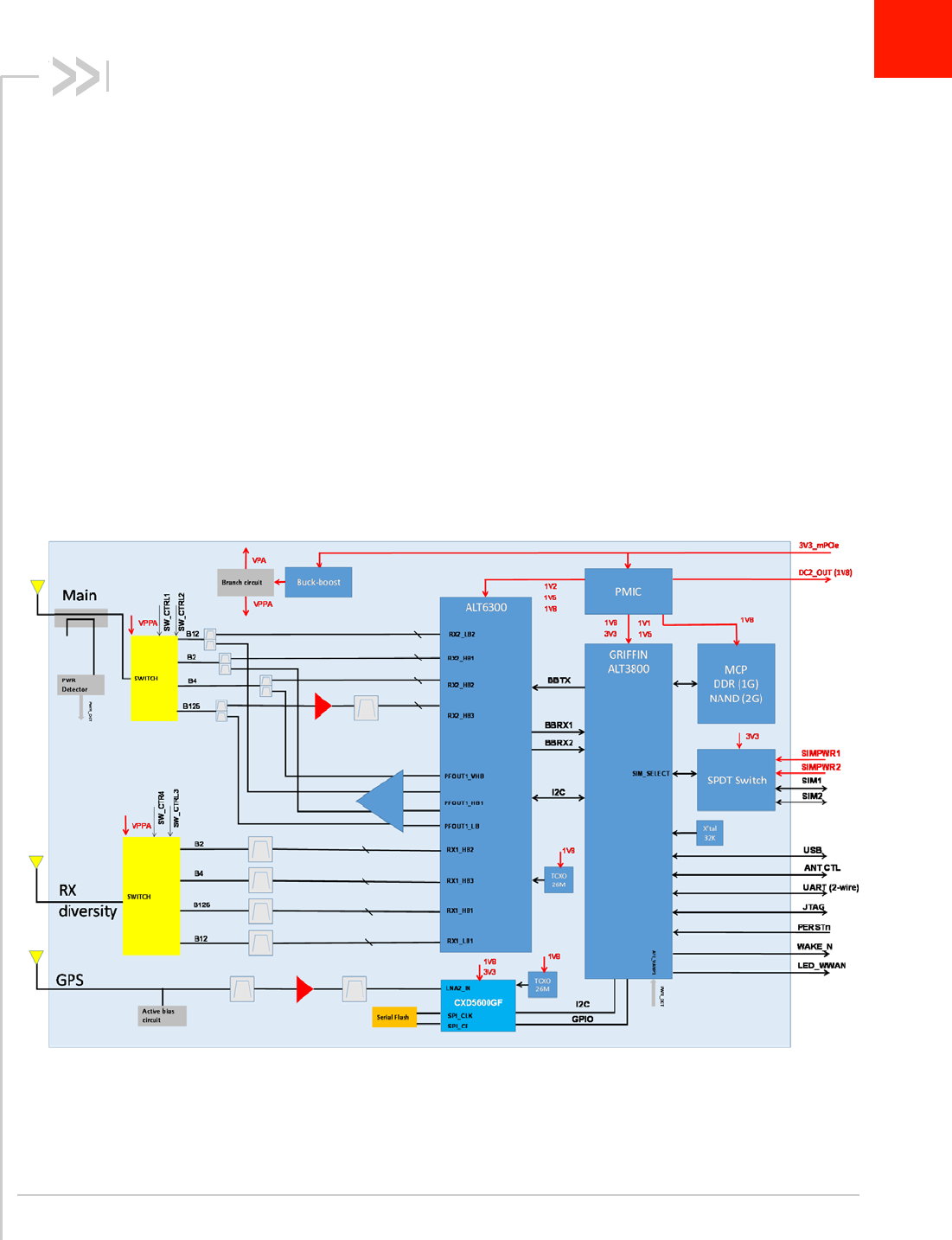
The system block diagram in Figure 3-1 on page 13 represents the MC7475 module
integrated into a host system. The module includes the following interfaces to the
host:
•Power—Supplied to the module by the host.
•WAKE_N— Signal used to wake the host when specific events occur.
•WAN_LED_N—Active-low LED drive signal provides an indication of RADIO ON
state, either WAN or GPS.
•SYSTEM_RESET_N—Active-low reset input.
•Antenna—Three U.FL RF connectors (main (Rx/Tx), GPS, and auxiliary (Rx
diversity). For details, see RF Specifications on page 24.
•Antenna control—Three signals that can be used to control external antenna
switches.
•Dual SIM—Supported through the interface connector. The SIM cavities /
connectors must be placed on the host device for this feature.
•USB—USB 2.0 interface to the host for data, control, and status information.
The MC7475 has two main interface areas—the host I/O connector and the RF
ports. Details of these interfaces are described in the sections that follow.
Figure 3-1: System Block Diagram
Product Technical Specification
Rev 3 Sep.17 14 41110251
Host Interface Pin Assignments
The MC7475 host I/O connector provides pins for power, serial communications,
and control. Pin assignments are listed in Table 3-1.
Refer to the following tables for pin details based on interface types:
•Table 3-2, Power and Ground Specifications, on page 18
•Table 3-3, USB Interfaces, on page 18
•Table 3-4, SIM Interface Signals, on page 19
•Table 3-5, Module Control Signals, on page 22
Note: On any given interface (USB, SIM, etc.), leave unused inputs and outputs as no-
connects.
Note: The host should not drive any signals to the module until the power-on sequence is
complete.
Table 3-1: Connector Pin Assignmentsa
Pin Signal name
Pin
typebDescription DirectioncActive
state
Voltage levels (V)
Min Typ Max
1WAKE_N OC Wake host Output Low - - 0.10
2VCC VPower supply Input Power 3.135 3.30 3.60
3ANT_CTRL0 /
GPIO1 -(ANT_CTRL0)
Customer-
defined external
switch control
for multiple
antennas
Output High 1.35 1.80 1.90
Output Low 0 - 0.8
(GPIO1)
General
purpose I/O
Input High 1.53 1.80 2.10
Input Low -0.30 0.45
Output High 1.35 1.80 1.90
Output Low 0.00 0.8
4GND VGround Input Power - 0 -
5ANT_CTRL1 /
GPIO2 -(ANT_CTRL1)
Customer-
defined external
switch control
for multiple
antennas
Output High 1.35 1.80 1.90
Output Low 0 - 0.8
(GPIO2)
General
purpose I/O
Input High 1.53 1.80 2.10
Input Low -0.30 0.45
Output High 1.35 1.80 1.90
Output Low 0.00 0.8
6NC -No connect - - - - -

Electrical Specifications
Rev 3 Sep.17 15 41110251
7USIM2_RST -SIM 2 Reset Output Low 0 - 0.45
High 2.55 (3V SIM)
1.35 (1.8V SIM)
-3.10 (3V SIM)
1.90 (1.8V SIM)
8USIM_PWR -SIM VCC supply Output Power 2.90 (3V SIM)
1.75 (1.8V SIM)
3.00 (3V SIM)
1.80 (1.8V SIM)
3.10 (3V SIM)
1.85 (1.8V SIM)
9GND VGround Input Power - 0 -
10 USIM_DATA -SIM IO pin Input Low -0.30 (3V SIM)
-0.30 (1.8V SIM)
-0.60 (3V SIM)
0.35 (1.8V SIM)
High 2.10 (3V SIM)
1.17 (1.8V SIM)
3.00 (3V SIM)
1.80 (1.8V SIM)
3.30 (3V SIM)
2.10 (1.8V SIM)
Output Low 0 - 0.40
High 2.55 (3V SIM)
1.35 (1.8V SIM)
3.00 (3V SIM)
1.80 (1.8V SIM)
3.10 (3V SIM)
1.90 (1.8V SIM)
11 VREF_1.8Vd-1.8V reference
voltage output Output Power 1.75 1.80 1.85
12 USIM_CLK -SIM Clock Output Low 0 - 0.45
High 2.55 (3V SIM)
1.35 (1.8V SIM)
3.00 (3V SIM)
1.80 (1.8V SIM)
3.10 (3V SIM)
1.90 (1.8V SIM)
13 USIM2_PWR -SIM 2 VCC
supply Output Power 2.90 (3V SIM)
1.75 (1.8V SIM)
3.00 (3V SIM)
1.80 (1.8V SIM)
3.10 (3V SIM)
1.85 (1.8V SIM)
14 USIM_RST -SIM Reset Output Low 0 - 0.45
High 2.55 (3V SIM)
1.35 (1.8V SIM)
3.00 (3V SIM)
1.80 (1.8V SIM)
3.10 (3V SIM)
1.90 (1.8V SIM)
15 GND VGround Input Power - 0 -
16 NC -No connect - - - - -
17 USIM2_CLK -SIM 2 Clock Output Low 0 - 0.45
High 2.55 (3V SIM)
1.35 (1.8V SIM)
3.00 (3V SIM)
1.80 (1.8V SIM)
3.10 (3V SIM)
1.90 (1.8V SIM)
18 GND VGround Input Power - 0 -
Table 3-1: Connector Pin Assignmentsa (Continued)
Pin Signal name
Pin
typebDescription DirectioncActive
state
Voltage levels (V)
Min Typ Max

Product Technical Specification
Rev 3 Sep.17 16 41110251
19 USIM2_DATA -SIM 2 IO pin Input Low -0.30 (3V SIM)
-0.30 (1.8V SIM)
-0.60 (3V SIM)
0.35 (1.8V SIM)
High 2.10 (3V SIM)
1.17 (1.8V SIM)
3.00 (3V SIM)
1.80 (1.8V SIM)
3.30 (3V SIM)
2.10 (1.8V SIM)
Output Low 0 - 0.40
High 2.55 (3V SIM)
1.35 (1.8V SIM)
3.00 (3V SIM)
1.80 (1.8V SIM)
3.10 (3V SIM)
1.90 (1.8V SIM)
20 NC -No connect - - - - -
21 GND VGround Input Power - 0 -
22 SYSTEM_RESET_NeOC Reset Input Low -0.30 -0.63
23 Reserved
24 VCC VPower supply Input Power 3.135 3.30 3.60
25 Reserved
26 GND VGround Input Power - 0 -
27 GND VGround Input Power - 0 -
28 NC -No connect - - - - -
29 GND VGround Input Power - 0 -
30 NC Reserved—
Host must not
repurpose this
pin.
31 Reserved
32 NC Reserved—
Host must not
repurpose this
pin.
33 Reserved
34 GND VGround Input Power - 0 -
35 GND VGround Input Power - 0 -
36 USB_D- -USB data
negative Input/Output Differential - - -
37 GND VGround Input Power - 0 -
38 USB_D+ -USB data
positive Input/Output Differential - - -
39 VCC VPower supply Input Power 3.135 3.30 3.60
40 GND VGround Input Power - 0 -
41 VCC VPower supply Input Power 3.135 3.30 3.60
Table 3-1: Connector Pin Assignmentsa (Continued)
Pin Signal name
Pin
typebDescription DirectioncActive
state
Voltage levels (V)
Min Typ Max

Electrical Specifications
Rev 3 Sep.17 17 41110251
42 WAN_LED_N OC LED Driver Output Low 0 - 0.15f
43 GND VGround Input Power - 0 -
44 ANT_CTRL2 /
GPIO3 -(ANT_CTRL2)
Customer-
defined external
switch control
for multiple
antennas
Output High 1.35 1.80 1.90
Output Low 0 - 0.8
(GPIO3)
General
purpose I/O
Input High 1.53 1.80 2.10
Input Low -0.30 0.45
Output High 1.35 1.80 1.90
Output Low 0.00 0.8
45 NC Reserved—
Host must not
repurpose this
pin.
46 ANT_CTRL3/
GPIO4 -(ANT_CTRL3)
Customer-
defined external
switch
Input High 1.35 1.80 1.90
Input Low 0 - 0.8
(GPIO4)
General
purpose I/O
Input High 1.53 1.80 2.10
Input Low -0.30 0.45
Output High 1.35 1.80 1.90
Output Low 0.00 0.8
47 NC Reserved—
Host must not
repurpose this
pin.
48 NC -No connect - - - - -
49 NC Reserved—
Host must not
repurpose this
pin.
50 GND VGround Input Power - 0 -
51 NC Reserved—
Host must not
repurpose this
pin.
52 VCC VPower supply Input Power 3.135 3.30 3.60
a. The host should leave all ‘NC’ (‘no connect) pins unconnected.
b. A—Analog; I—Input; NP—No pull; O—Digital output; OC—Open Collector; PU—Digital input (internal pull up); PD—Digital output
(internal pull down); V—Power or ground
c. Signal directions are from module’s point of view (e.g. ‘Output’ from module to host, ‘Input’ to module from host.)
d. To avoid adverse effects on module operation, do not draw more than 10 mA current on pin 11.
Table 3-1: Connector Pin Assignmentsa (Continued)
Pin Signal name
Pin
typebDescription DirectioncActive
state
Voltage levels (V)
Min Typ Max
Product Technical Specification
Rev 3 Sep.17 18 41110251
Power Supply
The host provides power to the MC7475 through multiple power and ground pins
as summarized in Table 3-2.
The host must provide safe and continuous power at all times; the module does
not have an independent power supply, or protection circuits to guard against
electrical issues.
USB Interface
Important: Host support for USB 2.0 signals is required.
The device supports a USB 2.0 interface for communication between the host and
module.
The interface complies with the [7] Universal Serial Bus Specification, Rev 2.0,
and the host device must be designed to the same standards (subject to details
shown in Table 3-3 below). (Note: When designing the host device, careful PCB
layout practices must be followed.)
USB Throughput Performance
This device has been designed to achieve optimal performance and maximum
throughput using USB high-speed mode (USB 2.0). Although the device may
operate with a high speed host, throughput performance will be on an “as is”
e. The module must not be plugged into a port that supports PCI Express—the pin is used by a PCIE signal, which can cause the
module to be in reset state or occasionally reset.
f. Max voltage level when current < 100 mA.
Table 3-2: Power and Ground Specifications
Name Pins Specification Min Typ Max Units
VCC 2, 24, 39, 41, 52 Voltage range See Table 3-1 on page 14.
Ripple voltage --100 mVpp
GND 4, 9, 15, 18, 21, 26,
27, 29, 34, 35, 37,
40, 43, 50
- - 0 - V
Table 3-3: USB Interfaces
Name Pin Description
USB 2.0 USB_D- 36 USB data negative
USB_D+ 38 USB data positive

Electrical Specifications
Rev 3 Sep.17 19 41110251
basis and needs to be characterized by the OEM. Note that throughput will be
reduced and may vary significantly based on packet size, host interface, and
firmware revision.
SIM Interface
Note: Host support for
SIM interface signals is
required.
The module supports up to two SIMs (Subscriber Identity Module) (1.8 V or 3 V).
Each SIM holds information for a unique account, allowing users to optimize their
use of each account on multiple devices.
The SIM pins (Table 3-4) provide the connections necessary to interface to SIM
sockets located on the host device as shown in Figure 3-2 on page 20. Voltage
levels over this interface comply with 3GPP standards.
The types of SIM connectors used depends on how the host device exposes the
SIM sockets.
Table 3-4: SIM Interface Signals
SIM Name Pin Description
SIM contact
numberaNotes
Primary USIM_PWR 8SIM voltage 1Power supply for SIM
USIM_DATA 10 Data I/O 7Bi-directional SIM data line
USIM_CLK 12 Serial clock 3Serial clock for SIM data
USIM_RST 14 Reset 2Active low SIM reset
USIM_GND Ground 5Ground reference
USIM_GND is common to module ground
Secondary USIM2_PWR 13 SIM voltage 2Power supply for SIM 2
USIM2_DATA 19 Data I/O 3Bi-directional SIM 2 data line
USIM2_CLK 17 Serial clock 7Serial clock for SIM 2 data
USIM2_RST 7Reset 1Active low SIM 2 reset
USIM2_GND SIM indication -Ground reference
USIM2_GND is common to module ground
a. See Figure 3-3 on page 20 for SIM card contacts.
Product Technical Specification
Rev 3 Sep.17 20 41110251
Figure 3-2: SIM Application Interface (applies to both SIM interfaces)
Figure 3-3: SIM Card Contacts (Contact View)
AirPrime
embedded
module
SIM card connector
(Optional.
Locate near the
SIM socket)
47 pF, 51
4.7uF
X5R
typ
(C1)
USIM_PWR
USIM_CLK
USIM_DATA
USIM_RST
Located near
SIM socket
Located near SIM socket.
NOTE: Carefully consider if ESD
protection is required – it may
increase signal rise time and
lead to certification failure
USIM_GND
ESD
protection
(C3)
(C7)
(C2)
(C5)
(Optional.
Locate near the
SIM socket)
15 k - 30 k
0.1uF
NOTE: UIM signals
refer to both USIM1
and USIM2.
C8
C7
C6
C5
C4
C3
C2
C1
GND VCC
VPP RST
I/O CLK
RFU RFU
Contact View (notched corner at top left)

Electrical Specifications
Rev 3 Sep.17 21 41110251
SIM Implementation
Note: For interface design
requirements, refer to ETSI
TS 102 230 V5.5.0, section
5.2.
When designing the remote SIM interface, you must make sure that SIM signal
integrity is not compromised.
Some design recommendations include:
•Total impedance of the VCC and GND connections to the SIM, measured at
the module connector, should be less than 1 to minimize voltage drop
(includes any trace impedance and lumped element components—inductors,
filters, etc.).
•Position the SIM connector 10 cm from the module. If a longer distance is
required because of the host device design, use a shielded wire assembly—
connect one end as close as possible to the SIM connector and the other end
as close as possible to the module connector. The shielded assembly may
help shield the SIM interface from system noise.
•Avoid routing the clock and data lines for each SIM (USIM_CLK/
USIM_DATA, USIM2_CLK/USIM2_DATA) in parallel over distances
2 cm—cross-coupling of a clock and data line pair can cause failures.
•3GPP has stringent requirements for I/O rise time (<1 µs), signal level limits,
and noise immunity—consider this carefully when developing your PCB
layout.
·Keep signal rise time <1 µs—keep SIM signals as short as possible, and
keep very low capacitance traces on the data and clock signals
(USIM_CLK, USIM_DATA, USIM2_CLK, USIM2_DATA). High capacitance
increases signal rise time, potentially causing your device to fail certification
tests.
•Add external pull-up resistors (15 k–30 k), if required, between the data
and power lines for each SIM (USIM_DATA/USIM_PWR, USIM2_DATA/
USIM2_PWR) to optimize the signal rise time.
•VCC line should be decoupled close to the SIM socket.
•SIM is specified to run up to 5 MHz (SIM clock rate). Take note of this speed
in the placement and routing of the SIM signals and connectors.
•You must decide whether additional ESD protection is required for your
product, as it is dependent on the application, mechanical enclosure, and SIM
connector design. The SIM pins will require additional ESD protection if they
are exposed to high ESD levels (i.e. can be touched by a user).
•Putting optional decoupling capacitors on the SIM power lines (USIM_PWR,
USIM2_PWR) near the SIM sockets is recommended—the longer the trace
length (impedance) from the socket to the module, the greater the capaci-
tance requirement to meet compliance tests.
•Putting an optional series capacitor and resistor termination (to ground) on
the clock lines (USIM_CLK, USIM2_CLK) at the SIM sockets to reduce EMI
and increase signal integrity is recommended if the trace length between the
SIM socket and module is long—47 pF and 50 resistor are recommended.
•Test your first prototype host hardware with a Comprion IT3 SIM test device
at a suitable testing facility.
Product Technical Specification
Rev 3 Sep.17 22 41110251
Control Interface (Signals)
The MC7475 provides signals for:
•Waking the host when specific events occur
•LED driver output
These signals are summarized in Table 3-5 and paragraphs that follow.
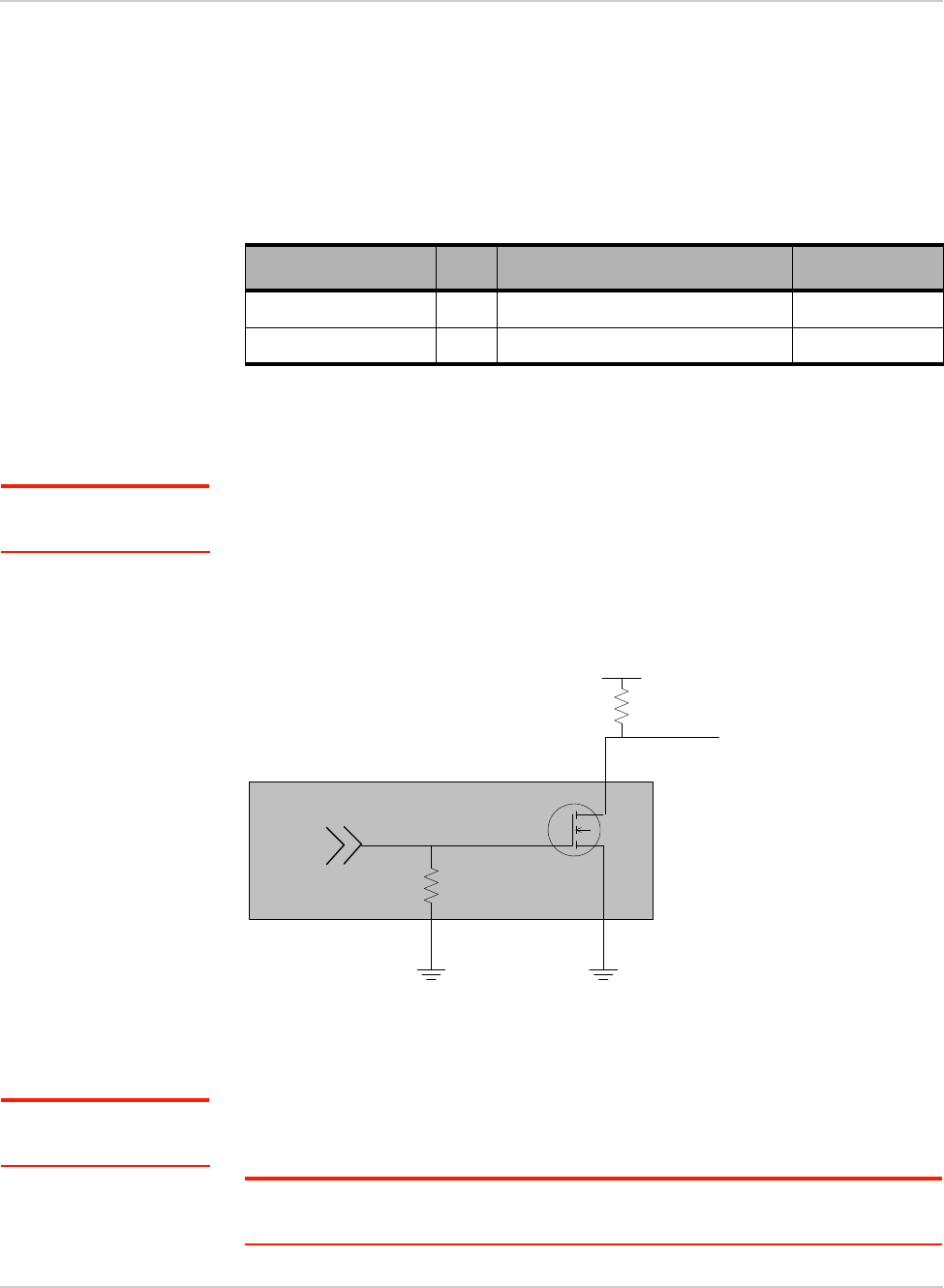
WAKE_N — Wake Host
Note: Host support for
WAKE_N is optional.
The module uses WAKE_N to wake the host when specific events occur.
The host must provide a 5 k–100 k pullup resistor that considers total line
capacitance (including parasitic capacitance) such that when WAKE_N is
deasserted, the line will rise to 3.3 V (Host power rail) in < 100 ns.
See Figure 3-4 on page 22 for a recommended implementation.
Figure 3-4: Recommended WAKE_N Connection
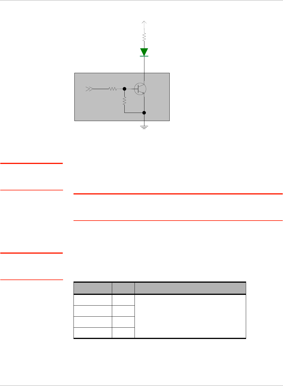
WAN_LED_N—LED Output
Note: Host support for
WAN_LED_N is optional.
The module drives the LED output according to [6] PCI Express Mini Card
Electromechanical Specification Revision 2.1.
Note: The LED configuration is customizable. Contact your Sierra Wireless account repre-
sentative for details.
Table 3-5: Module Control Signals
Name Pin Description Typea
a. OC—Open Collector; PU—Digital pin Input, internal pull up
WAKE_N 1Wake host OC
WAN_LED_N 42 LED driver OC
Control
R
WAKE_N
1
2
3
Q
5k-100k
Host
VCC
MiniCard
Electrical Specifications
Rev 3 Sep.17 23 41110251
Figure 3-5: Example LED
SYSTEM_RESET_N—Reset Input
Note: Host support for
SYSTEM_RESET_N is
optional.
SYSTEM_RESET_N has an internal 1.8 V internal pull up that requires an open
collector input from the host. Set this signal to active low to reset the device. Note
that the minimum pulse width is 2 s.
Note: The module must not be plugged into a port that supports PCI Express—
SYSTEM_RESET_N is carried on a pin that is used for a PCIE signal, which can cause
the module to be in reset state or occasionally reset.
Antenna Control
Note: Host support for
antenna control signals is
optional.
The MC7475 Mini Card provides three output signals (listed in Table 3-6) that may
be used for host designs that incorporate tunable antennas.
Current limiting Resistor
LED
VCC
MIO
MiniCard WAN_LED_N
Table 3-6: Antenna Control Signals
Name Pin Description
ANT_CTRL0 3Customer-defined external switch control for
tunable antennas
ANT_CTRL1 5
ANT_CTRL2 44
ANT_CTRL3 46
Rev 3 Sep.17 24 41110251
4
4: RF Specifications
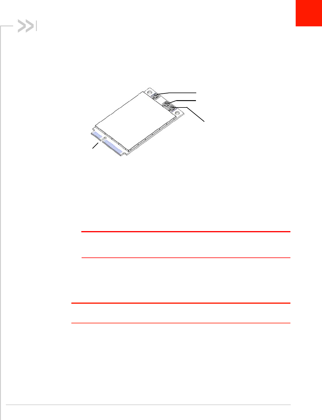
The MC7475 includes three RF connectors for use with host-supplied antennas:
•Main RF connector—Tx/Rx path
•GPS RF connector—Dedicated GPS
•Auxiliary RF connector—Rx diversity
The module does not have integrated antennas.
Figure 4-1: Module Connectors
RF Connections
When attaching antennas to the module:
•Use Hirose U.FL connectors (3 mm x 3 mm, low profile; model
U.FL #CL331-0471-0-10) to attach antennas to connection points on the module,
as shown in Figure 4-1 on page 24.
Note: To disconnect the antenna, make sure you use the Hirose U.FL connector
removal tool (P/N UFL-LP-N-2(01)) to prevent damage to the module or coaxial cable
assembly.
•Match coaxial connections between the module and the antenna to 50 .
•Minimize RF cable losses to the antenna; the recommended maximum cable
loss for antenna cabling is 0.5 dB.
•To ensure best thermal performance, mounting holes must be used to attach
(ground) the device to the main PCB ground or a metal chassis.
Note: If the antenna connection is shorted or open, the modem will not sustain permanent
damage.
Shielding
The module is fully shielded to protect against EMI and the shield must not be
removed.
I/O connector
Main RF connector
GPS RF connector
Auxiliary (Rx diversity)
RF connector

RF Specifications
Rev 3 Sep.17 25 41110251
Antenna and Cabling
When selecting the antenna and cable, it is critical to RF performance to optimize
antenna gain and cable loss.
Note: For detailed electrical performance criteria, see Appendix 8: Antenna Specification
on page 43.
Choosing the Correct Antenna and Cabling
When matching antennas and cabling:
•The antenna (and associated circuitry) should have a nominal impedance of
50 with a recommended return loss of better than 10 dB across each
frequency band of operation.
•The system gain value affects both radiated power and regulatory (FCC) test
results.
Designing Custom Antennas
Consider the following points when designing custom antennas:
•A skilled RF engineer should do the development to ensure that the RF
performance is maintained.
•If both CDMA and UMTS modules will be installed in the same platform, you
may want to develop separate antennas for maximum performance.
Determining the Antenna’s Location
When deciding where to put the antennas:
•Antenna location may affect RF performance. Although the module is
shielded to prevent interference in most applications, the placement of the
antenna is still very important—if the host device is insufficiently shielded,
high levels of broadband noise or spurious interference can degrade the
module’s performance.
•Connecting cables between the module and the antenna must have 50
impedance. If the impedance of the module is mismatched, RF performance
is reduced significantly.
•Antenna cables should be routed, if possible, away from noise sources
(switching power supplies, LCD assemblies, etc.). If the cables are near the
noise sources, the noise may be coupled into the RF cable and into the
antenna. See Interference From Other Wireless Devices on page 26.
Ground Connection
When connecting the module to system ground:
•Prevent noise leakage by establishing a very good ground connection to the
module through the host connector.
•Connect to system ground using the two mounting holes at the top of the
module (shown in Figure 4-1 on page 24).
•Minimize ground noise leakage into the RF.
Depending on the host board design, noise could potentially be coupled to

Product Technical Specification
Rev 3 Sep.17 26 41110251
the module from the host board. This is mainly an issue for host designs that
have signals traveling along the length of the module, or circuitry operating at
both ends of the module interconnects.
Interference and Sensitivity
Several interference sources can affect the module’s RF performance
(RF desense). Common sources include power supply noise and device-
generated RF.
RF desense can be addressed through a combination of mitigation techniques
(Methods to Mitigate Decreased Rx Performance on page 27) and radiated
sensitivity measurement (Radiated Sensitivity Measurement on page 27).
Interference From Other Wireless Devices
Wireless devices operating inside the host device can cause interference that
affects the module.
To determine the most suitable locations for antennas on your host device,
evaluate each wireless device’s radio system, considering the following:
•Any harmonics, sub-harmonics, or cross-products of signals generated by
wireless devices that fall in the module’s Rx range may cause spurious
response, resulting in decreased Rx performance.
•The Tx power and corresponding broadband noise of other wireless devices
may overload or increase the noise floor of the module’s receiver, resulting in
Rx desense.
The severity of this interference depends on the closeness of the other antennas
to the module’s antenna. To determine suitable locations for each wireless
device’s antenna, thoroughly evaluate your host device’s design.
Host-generated RF Interference
All electronic computing devices generate RF interference that can negatively
affect the receive sensitivity of the module.
Proximity of host electronics to the antenna in wireless devices can contribute to
decreased Rx performance. Components that are most likely to cause this
include:
•Microprocessor and memory
•Display panel and display drivers
•Switching-mode power supplies
Device-generated RF Interference
The module can cause interference with other devices. Wireless devices such as
AirPrime embedded modules transmit in bursts (pulse transients) for set durations
(RF burst frequencies). Hearing aids and speakers convert these burst
frequencies into audible frequencies, resulting in audible noise.

RF Specifications
Rev 3 Sep.17 27 41110251
Methods to Mitigate Decreased Rx
Performance
It is important to investigate sources of localized interference early in the design
cycle. To reduce the effect of device-generated RF on Rx performance:
•Put the antenna as far as possible from sources of interference. The
drawback is that the module may be less convenient to use.
•Shield the host device. The module itself is well shielded to avoid external
interference. However, the antenna cannot be shielded for obvious reasons.
In most instances, it is necessary to employ shielding on the components of
the host device (such as the main processor and parallel bus) that have the
highest RF emissions.
•Filter out unwanted high-order harmonic energy by using discrete filtering on
low frequency lines.
•Form shielding layers around high-speed clock traces by using multi-layer
PCBs.
•Route antenna cables away from noise sources.
Radiated Spurious Emissions (RSE)
When designing an antenna for use with AirPrime embedded modules, the host
device with an AirPrime embedded module must satisfy any applicable
standards/local regulatory bodies for radiated spurious emission (RSE) for
receive-only mode and for transmit mode (transmitter is operating).
Note that antenna impedance affects radiated emissions, which must be
compared against the conducted 50-ohm emissions baseline. (AirPrime
embedded modules meet the 50-ohm conducted emissions requirement.)
Radiated Sensitivity Measurement
A wireless host device contains many noise sources that contribute to a reduction
in Rx performance.
To determine the extent of any receiver performance desensitization due to self-
generated noise in the host device, over-the-air (OTA) or radiated testing is
required. This testing can be performed by Sierra Wireless or you can use your
own OTA test chamber for in-house testing.
Sierra Wireless’ Sensitivity Testing and
Desensitization Investigation
Although AirPrime embedded modules are designed to meet network operator
requirements for receiver performance, they are still susceptible to various
performance inhibitors.
As part of the Engineering Services package, Sierra Wireless offers modem OTA
sensitivity testing and desensitization (desense) investigation. For more
information, contact your account manager or the Sales Desk (see Contact
Information on page 3).
Product Technical Specification
Rev 3 Sep.17 28 41110251
Note: Sierra Wireless has the capability to measure TIS (Total Isotropic Sensitivity) and
TRP (Total Radiated Power) according to CTIA's published test procedure.
Sensitivity vs. Frequency
For LTE bands, sensitivity is defined as the RF level at which throughput is 95% of
maximum.
Supported Frequencies
The MC7475 supports:
•Multiple-band LTE—See Table 4-1 on page 28 (supported bands)
•GPS
Conducted Rx Sensitivity / Tx Power
Table 4-1: LTE Frequency Bands
Band Frequency (Tx) Frequency (Rx)
Band 2 1850–1910 MHz 1930–1990 MHz
Band 4 1710–1755 2110–2155 MHz
Band 12 699–716 MHz 729–746 MHz
Band 125 2315–2318 MHz 2347–2350 MHz
Table 4-2: Conducted Rx (Receive) Sensitivity—LTE Bands
LTE bands Bandwidth
(MHz) Conducted Rx
sensitivity (dBm)
LTE Band 2 5-100.6
LTE Band 4 5-102.8
LTE Band 12 5-103.2
LTE Band 125 3-102.6
Table 4-3: Conducted Tx (Transmit) Power Tolerances
Parameter Conducted transmit power Notes
LTE
LTE Band 2,4,12 +23 dBm 1dB
LTE Band 125 +13 dBm 1dB QPSK full RB
RF Specifications
Rev 3 Sep.17 29 41110251
GPS Specifications
Note: For detailed electrical performance criteria, see Recommended GPS Antenna
Specifications on page 45.
Table 4-4: GPS Specifications
Parameter/feature Description
Satellite channels Maximum 12 channels, simultaneous tracking
Protocols NMEA 0183 V3.0
Acquisition time Hot start: 5 s
Cold start: 37 s
Note: Measured with signal strength = -135 dBm.
Sensitivity Trackinga: -160 dBm
Acquisition (Standalone)b: -145 dBm
a. Tracking sensitivity is the lowest GPS signal level for which the device can still detect an
in-view satellite 50% of the time when in sequential tracking mode.
b. Acquisition sensitivity is the lowest GPS signal level for which the device can still detect an
in-view satellite 50% of the time.
Operational limits Altitude <6000 m or velocity <100 m/s
(Either limit may be exceeded, but not both.)
Rev 3 Sep.17 30 41110251
5
5: Power
Power Consumption
Power consumption measurements in the tables below are for the MC7475 Mini Card
module connected to the host PC via USB.
The module does not have its own power source and depends on the host device for
power. For a description of input voltage requirements, see Power Supply on
page 18.
Table 5-1: Averaged Standby DC Power Consumption
Signal Description Bandsa
Current Notes /
configuration
Typ MaxbUnit
VCC Standby current consumption (Sleep mode deactivatedc)
LTE Band 2 13.5 21 mA DRX cycle = 8 (2.56 s)
Band 4 13.5 22 mA
Band 12 13 22 mA
Band 125 13 21 mA
a. For supported bands, see Table 4-1, LTE Frequency Bands, on page 28.
b. Measured at nominal 3.3 V voltage.
c. Assumes USB bus is fully suspended during measurements
Power
Rev 3 Sep.17 31 41110251
Power Interface
Power Ramp-up
On initial power up, inrush current depends on the power supply rise time—turn
on time >100 µs is required for < 3A inrush current.
The supply voltage must remain within specified tolerances while this is occurring.
Power-On/Off Timing
Figure 5-1 describes the timing sequence for powering the module on and off.
Note: The host should not drive any signals to the module until the power-on sequence is
complete.
Table 5-2: Averaged Call Mode DC Power Consumption
Description Tx power Band
Currenta
NotesTyp Unit
LTE 23 dBm B2/B4 900 mA 100/50 Mbps, 20 MHz BW
B12 828 mA 60/25 Mbps, 10 MHz BW
B125 647 mA 7.2/12.6 Mbps, 3 MHz BW
Peak current
(averaged over 100 s) 1012 mA All LTE bands
a. Measured at 25ºC/nominal 3.3 V voltage
Table 5-3: Miscellaneous DC Power Consumption
Signal Description
Current/Voltage
Unit Notes/configurationMin Typ Max
VCC Maximum current — — 1.5 A•Across all bands, all temperature ranges
•3.3 V supply
GPS Signal
connector Active bias on GPS port
— — 100 mA •See GPS RF connector in Figure 4-1 on
page 24
•GNSS active antenna specifications:
·DC voltage range: 3.0–3.25 V
·Within specified DC voltage range,
MC7475 will drive current up to 100 mA
(depending on antenna load).
·Specifications valid over operating input
DC voltage (VCC) and temperature
range.
3.00 3.15 3.25 V
Product Technical Specification
Rev 3 Sep.17 32 41110251
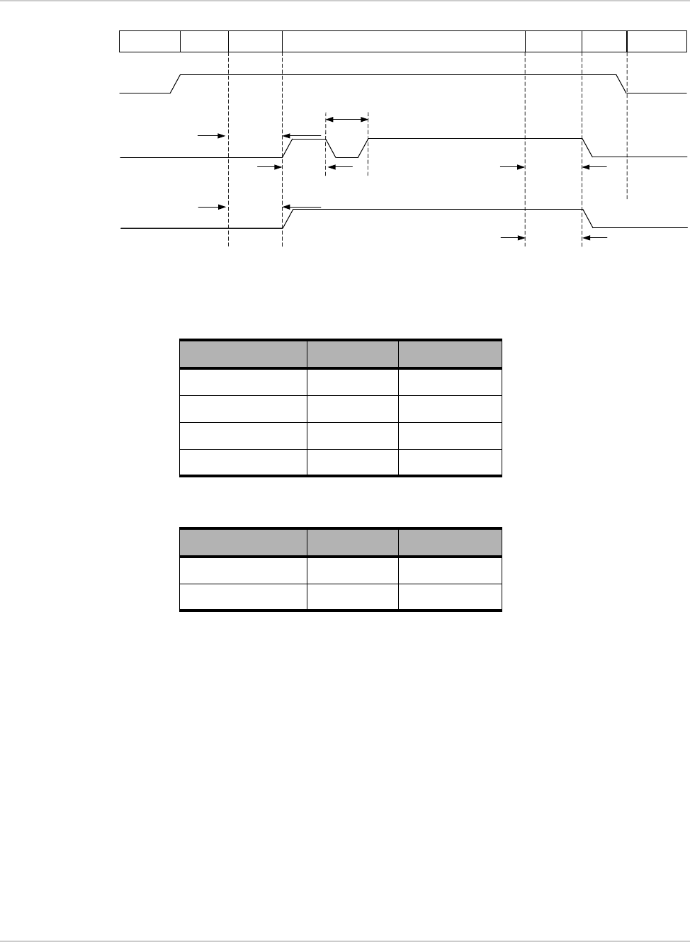
Figure 5-1: Signal Timing (USB Enumeration)
USB Enumeration
The unit supports single and double USB enumeration with the host:
•Single enumeration:
·Enumeration starts within maximum t_pwr_on_seq seconds of power-on.
•Double enumeration—As shown in Figure 5-1 on page 32:
·First enumeration starts within t_pwr_on_seq seconds of power-on (while
USB_D+ is high)
·Second enumeration starts after t_USB_suspend (when USB_D+ goes
high again)
Disconnected Power-on
Sequence
USB_D+
(Double enumeration)
Power-off
Sequence Disconnected
Active
DEVICE STATE
High
Low
Off Off
High
VCC Low
t_pwr_on_seq
t_USB_active
t_USB_suspend
t_pwr_off_seq
USB_D+
(Single enumeration)
High
Low
t_pwr_on_seq
t_pwr_off_seq
Table 5-4: USB 2.0 Power-On/Off Timing Parameters (Double
Enumeration)
Parameter Typical (s) Maximum (s)
t_pwr_on_seq TBD TBD
t_USB_active TBD TBD
t_USB_suspend TBD TBD
t_pwr_off_seq TBD TBD
Table 5-5: USB 2.0 Power-On/Off Timing Parameters (Single
Enumeration)
Parameter Typical (s) Maximum (s)
t_pwr_on_seq TBD TBD
t_pwr_off_seq TBD TBD

Power
Rev 3 Sep.17 33 41110251
Power Supply Noise
Noise in the power supply can lead to noise in the RF signal.
The power supply ripple limit for the module is no more than 100 mVp-p 1 Hz to
100 kHz. This limit includes voltage ripple due to transmitter burst activity.
Additional decoupling capacitors can be added to the main VCC line to filter noise
into the device.
Rev 3 Sep.17 34 41110251
6
6: Mechanical and Environmental Speci-
fications
The MC7475 module complies with the mechanical and environmental specifications
in Table 6-1. Final product conformance to these specifications depends on the OEM
device implementation.
Table 6-1: Mechanical and Environmental Specifications
Mode Details
Ambient temperature Operational
Class A -20ºC to +70ºC – 3GPP compliant
Operational
Class B -30ºC to +85ºC – non-3GPP compliant (reduced
operating parameters required)
Non-operational -40ºC to +85ºC, 96 hours
(from MIL-STD 202 Method 108)
Relative humidity Non-operational 85ºC, 85% relative humidity for 48 hours
(non-condensing)
Vibration Non-operational Random vibration, 10 to 2000 Hz, 0.1 g2/Hz to 0.0005 g2/
Hz, in each of three mutually perpendicular axes. Test
duration of 60 minutes for each axis, for a total test time of
three hours.
Shock Non-operational Half sine shock, 11 ms, 30 g, 8x each axis.
Half sine shock, 6 ms, 100 g, 3x each axis.
Drop Non-operational 1 m on concrete on each of six faces, two times (module
only).
Thermal considerations See Thermal Considerations on page 37.
Form factor PCI-Express Mini Card shielded with metal and metalized
fabric (F2 specification)
Dimensions Length: 50.8 mm
Width: 29.85 mm
Thickness: 2.75 mm (max)
Weight: 8.7 g
Mechanical and Environmental Specifications
Rev 3 Sep.17 35 41110251
Device Views
Figure 6-1: Top View
Figure 6-2: Dimensioned View
(Note: All dimensions shown in mm.)
50.8±0.15
48.05±0.1
4±0.1
2.6±0.1 29.85±0.15
24.2±0.1
8.25±0.1
3.85±0.1
1.65±0.1
4±0.05
13.6±0.05
5.6±0.05
1.5±0.1
PIN #1
PIN #51
2.55±0.1 TYP
0.25±0.1 MAX
0.6±0.05 TYP
2.6 +0.15
-0.10
4.88±0.25
14.5±0.25
19.29±0.25
1±0.1
1.6 +0.15
-0.05
TOP SIDE
0.8±0.03 pitch TYP
Product Technical Specification
Rev 3 Sep.17 36 41110251
Labeling
Figure 6-3: Sample Unit Label
Note: The displayed label is an example only. The production label will vary by SKU.
The MC7475 label is non-removable and contains:
•Sierra Wireless logo and product name
•IMEI number in Code-128 barcode format
•SKU number (when required)
•Factory Serial Number (FSN) in alphanumeric format
•Manufacturing date code (incorporated into FSN)
•Licensed vendor logo
•Applicable certification marks/details (e.g. FCC ID, etc. Example shows
FCC ID.)
Note: The MC7475 supports OEM partner-specific label requirements.
Electrostatic Discharge (ESD)
The OEM is responsible for ensuring that the Mini Card host interface pins are not
exposed to ESD during handling or normal operation. (See Table 6-1 on page 34
for specifications.)
ESD protection is highly recommended for the SIM connector at the point where
the contacts are exposed, and for any other signals from the host interface that
would be subjected to ESD by the user of the product. (The device includes ESD
protection on the antenna.)
FCC ID: N7Nxxxxxx
PRODUCT OF CHINA
FPPDDDYNNNNHH |||||||||||||||||||||||||||||||||||
BB
IMEI # 352678011234569
MC7430
Mechanical and Environmental Specifications
Rev 3 Sep.17 37 41110251
Thermal Considerations
Embedded modules can generate significant amounts of heat that must be
dissipated in the host device for safety and performance reasons.
Figure 6-4: Shield locations (Top view)
The amount of thermal dissipation required depends on:
•Supply voltage—Maximum power dissipation for the module can be up to
3.5 W at voltage supply limits.
•Usage—Typical power dissipation values depend on the location within the
host product, throughput, amount of data transferred, etc.
Specific areas requiring heat dissipation are shown in Figure 6-4:
•RF—Bottom face of module near RF connectors. Likely to be the hottest
area.
•Baseband—Bottom face of module, below the baseband area.
To enhance heat dissipation:
•It is recommended to add a heat sink that mounts the module to the main
PCB or metal chassis (a thermal compound or pads must be used between
the module and the heat sink).
RF
Baseband
Product Technical Specification
Rev 3 Sep.17 38 41110251
Figure 6-5: Copper Pad Location on Bottom Side of Module
•Maximize airflow over/around the module.
•Locate the module away from other hot components.
•Module mounting holes must be used to attach (ground) the device to the
main PCB ground or a metal chassis.
•You may also need active cooling to pull heat away from the module.
Note: Adequate dissipation of heat is necessary to ensure that the module functions
properly.
Module Integration Testing
When testing your integration design:
•Test to your worst case operating environment conditions (temperature and
voltage)
•Test using worst case operation (transmitter on 100% duty cycle, maximum
power)
•Monitor temperature on the underside of the module. Attach thermocouples
to the areas indicated in Figure 6-4 on page 37 (Baseband, RF).
Note: Make sure that your system design provides sufficient cooling for the module—
proper mounting, heat sinks, and active cooling may be required, depending on the
integrated application.
The internal module temperature must be kept to <90°C when integrated to prevent
damage to the module’s components. For best performance, keep the internal module
temperature below 80°C.
29.5±0.2
Copper Pad

Mechanical and Environmental Specifications
Rev 3 Sep.17 39 41110251
(For acceptance, certification, quality, and production (including RF) test
suggestions, see Testing on page 15.)

Rev 3 Sep.17 40 41110251
7
7: Regulatory Compliance and Industry
Certifications
This module is designed to meet, and upon commercial release, will meet the
requirements of the following regulatory bodies and regulations, where applicable:
•Federal Communications Commission (FCC) of the United States
Upon commercial release, the following industry certifications will have been
obtained, where applicable:
•PTCRB
Additional certifications and details on specific country approvals may be obtained
upon customer request—contact your Sierra Wireless account representative for
details.
Additional testing and certification may be required for the end product with an
embedded MC7475 module and are the responsibility of the OEM. Sierra Wireless
offers professional services-based assistance to OEMs with the testing and
certification process, if required.
Important Notice
Because of the nature of wireless communications, transmission and reception of
data can never be guaranteed. Data may be delayed, corrupted (i.e., have errors) or
be totally lost. Although significant delays or losses of data are rare when wireless
devices such as the Sierra Wireless module are used in a normal manner with a well-
constructed network, the Sierra Wireless module should not be used in situations
where failure to transmit or receive data could result in damage of any kind to the
user or any other party, including but not limited to personal injury, death, or loss of
property. Sierra Wireless and its affiliates accept no responsibility for damages of any
kind resulting from delays or errors in data transmitted or received using the Sierra
Wireless module, or for failure of the Sierra Wireless module to transmit or receive
such data.
Safety and Hazards
Do not operate your MC7475 module:
•In areas where blasting is in progress
•Where explosive atmospheres may be present including refuelling points, fuel
depots, and chemical plants
•Near medical equipment, life support equipment, or any equipment which may
be susceptible to any form of radio interference. In such areas, the MC7475
module MUST BE POWERED OFF. Otherwise, the MC7475 module can
transmit signals that could interfere with this equipment.
In an aircraft, the MC7475 module MUST BE POWERED OFF. Otherwise, the
MC7475 module can transmit signals that could interfere with various onboard
systems and may be dangerous to the operation of the aircraft or disrupt the cellular
Regulatory Compliance and Industry Certifications
Rev 3 Sep.17 41 41110251
network. Use of a cellular phone in an aircraft is illegal in some jurisdictions.
Failure to observe this instruction may lead to suspension or denial of cellular
telephone services to the offender, or legal action or both.
Some airlines may permit the use of cellular phones while the aircraft is on the
ground and the door is open. The MC7475 module may be used normally at this
time.
Important Compliance Information for the
United States of America
Note: Details are preliminary and subject to change.
The MC7475 module, upon commercial release, will have been granted modular
approval for mobile and fixed applications. Integrators may use the MC7475
module in their final products without additional FCC certification if they meet the
following conditions. Otherwise, additional FCC approvals must be obtained.
1. At least 20 cm separation distance between the antenna and the user’s body
must be maintained at all times.
2. To comply with FCC regulations limiting both maximum RF output power and
human exposure to RF radiation, the maximum antenna gain including cable
loss in a mobile-only exposure condition must not exceed the limits stipulated
in Table 7-1 on page 41.
Important: Mobile carriers often have limits on total radiated power (TRP), which
requires an efficient antenna. The end product with an embedded module must output
sufficient power to meet the TRP requirement but not too much to exceed FCC EIRP limit.
If you need assistance in meeting this requirement, please contact Sierra Wireless.
3. The MC7475 module may transmit simultaneously with other collocated radio
transmitters within a host device, provided the following conditions are met:
·Each collocated radio transmitter has been certified by FCC for mobile
application.
·At least 20 cm separation distance between the antennas of the collocated
transmitters and the user’s body must be maintained at all times.
Table 7-1: Antenna Gain Specifications
Device Technology Band Frequency
(MHz) Maximum antenna gain
(dBi)
MC7475 Mini Card LTE 21850–1910 6
41710–1755 6
12 699–716 6
125 2315–2318 10
Product Technical Specification
Rev 3 Sep.17 42 41110251
·The output power and antenna gain in a collocated configuration must not
exceed the limits and configurations stipulated in Table 7-2.
4. A label must be affixed to the outside of the end product into which the
MC7475 module is incorporated, with a statement similar to the following:
· This device contains FCC ID: N7NMC7475.
5. A user manual with the end product must clearly indicate the operating
requirements and conditions that must be observed to ensure compliance
with current FCC RF exposure guidelines.
The end product with an embedded MC7475 module may also need to pass the
FCC Part 15 unintentional emission testing requirements and be properly
authorized per FCC Part 15.
Note: If this module is intended for use in a portable device, you are responsible
for separate approval to satisfy the SAR requirements of FCC Part 2.1093.
Note: Per FCC Part 27, mobile and portable stations containing MC7475
modules are not permitted to transmit using LTE B125 (2315–2318 MHz).
Table 7-2: Collocated Radio Transmitter Specifications
Device Technology Frequency
(MHz) EIRP Limit
(dBm)
Collocated
transmittersa
a. Valid collocated transmitter combinations: WLAN+BT; WiMAX+BT.
(WLAN+WiMAX+BT is not permitted.)
WLAN 2400–2500 23
5150–5850 23
WiMAX 2300–2400 25
2500–2700 25
3300–3800 25
BT 2400–2500 15
Rev 3 Sep.17 43 41110251
8
8: Antenna Specification
This appendix describes recommended electrical performance criteria for main path,
Rx diversity path, and GPS antennas used with AirPrime embedded modules.
The performance specifications described in this section are valid while antennas are
mounted in the host device with antenna feed cables routed in their final application
configuration.
Note: Antennas should be designed before the industrial design is finished to make sure that
the best antennas can be developed.
Recommended Main/Rx Diversity Antenna
Specifications
Table 8-1: Antenna Requirements a
Parameter Requirements Comments
Antenna system External multi-band antenna
system with Rx diversity (Ant1/
Ant2)b
Operating bands—
Antenna 1 669–746 MHz
1710–1990 MHz
2110–2155 MHz
2315–2350 MHz
Operating bands—
Antenna 2 729–746 MHz
1930–1990 MHz
2110–2155 MHz
2347–2350 MHz
VSWR of Ant1 and Ant2 •< 2:1 (recommended)
•< 3:1 (worst case)
On all bands including band edges

Product Technical Specification
Rev 3 Sep.17 44 41110251
Total radiated efficiency of
Ant1 and Ant2 > 50% on all bands •Measured at the RF connector.
•Includes mismatch losses, losses in the
matching circuit, and antenna losses,
excluding cable loss.
•Sierra Wireless recommends using
antenna efficiency as the primary
parameter for evaluating the antenna
system.
Peak gain is not a good indication of
antenna performance when integrated
with a host device (the antenna does not
provide omni-directional gain patterns).
Peak gain can be affected by antenna
size, location, design type, etc.—the
antenna gain patterns remain fixed unless
one or more of these parameters change.
Radiation patterns of Ant1
and Ant2 Nominally Omni-directional
radiation pattern in azimuth plane.
Envelope correlation
coefficient between Ant1
and Ant2
•< 0.4 on low Rx bands (up to
1500 MHz)
•< 0.2 on high Rx bands (over
1500 MHz)
Mean Effective Gain of
Ant1 and Ant2 (MEG1,
MEG2)
-3 dBi
Ant1 and Ant2 Mean
Effective Gain Imbalance I
MEG1 / MEG2 I
< 6 dB for Rx diversity operation
Maximum antenna gain Must not exceed antenna gains
due to RF exposure and ERP/
EIRP limits, as listed in the
module’s FCC grant.
See Important Compliance Information for the
United States of America on page 41.
Isolation between Ant1 and
Ant2 (S21) > 10 dB •If antennas can be moved, test all
positions for both antennas.
•Make sure all other wireless devices
(Bluetooth or WLAN antennas, etc.) are
turned OFF to avoid interference.
Power handling •> 2 W RF power on low bands
•> 1 W on high bands
•Measure power endurance over 4 hours
(estimated talk time) using a 2 W CW
signal—set the CW test signal frequency
to the middle of the PCS Tx band
(1880 MHz for PCS).
•Visually inspect device to ensure there is
no damage to the antenna structure and
matching components.
•VSWR/TIS/TRP measurements taken
before and after this test must show
similar results.
Table 8-1: Antenna Requirements (Continued)a
Parameter Requirements Comments

Antenna Specification
Rev 3 Sep.17 45 41110251
Recommended GPS Antenna
Specifications
Antenna Tests
The following guidelines apply to the requirements described in Table 8-1 on
page 43 and Table 8-2 on page 45:
•Perform electrical measurements at room temperature (+20°C to +26°C)
unless otherwise specified
•For main and Rx diversity path antennas, make sure the antennas (including
contact device, coaxial cable, connectors, and matching circuit with no more
than six components, if required) have nominal impedances of 50 across
supported frequency bands.
a. These worst-case VSWR figures for the transmitter bands may not guarantee RSE levels to be within regulatory limits. The
device alone meets all regulatory emissions limits when tested into a cabled (conducted) 50 ohm system. With antenna
designs with up to 2.5:1 VSWR or worse, the radiated emissions could exceed limits. The antenna system may need to be
tuned in order to meet the RSE limits as the complex match between the module and antenna can cause unwanted levels of
emissions. Tuning may include antenna pattern changes, phase/delay adjustment, passive component matching. Examples of
the application test limits would be included in FCC Part 22, Part 24 and Part 27, test case 4.2.2 for WCDMA
(ETSI EN 301 908-1), where applicable.
b. Ant1—Primary, Ant2—Secondary (Rx Diversity)
Table 8-2: GPS Antenna Requirements
Parameter Requirements Comments
Frequency range 1575.42 MHz ±2MHz minimum
Field of view (FOV) •Omni-directional in azimuth
•-45° to +90° in elevation
Polarization
(average Gv/Gh) >0dB Vertical linear polarization is
sufficient.
Free space average gain
(Gv+Gh) over FOV > -6 dBi (preferably > -3 dBi) Gv and Gh are measured
and averaged over -45° to
+90° in elevation, and ±180°
in azimuth.
Gain •Maximum gain and uniform
coverage in the high elevation
angle and zenith.
•Gain in azimuth plane is not
desired.
Average 3D gain >-5dBi
Isolation between GPS and
Ant1 > 10 dB in all uplink bands
Typical VSWR < 2.5:1
Polarization Any other than LHCP (left-hand
circular polarized) is acceptable.

Product Technical Specification
Rev 3 Sep.17 46 41110251
•All tests (except isolation/correlation coefficient)—Test the main or Rx
diversity antenna with the other antenna terminated.
•Any metallic part of the antenna system that is exposed to the outside
environment needs to meet the electrostatic discharge tests per IEC61000-4-
2 (conducted discharge +8kV).
•The functional requirements of the antenna system are tested and verified
while the embedded module’s antenna is integrated in the host device.
Note: Additional testing, including active performance tests, mechanical, and accelerated
life tests can be discussed with Sierra Wireless’ engineering services. Contact your Sierra
Wireless representative for assistance.
Rev 3 Sep.17 47 41110251
9
9: Design Checklist
This chapter provides a summary of the design considerations mentioned throughout
this guide. This includes items relating to the power interface, RF integration, thermal
considerations, cabling issues, and so on.
Note: This is NOT an exhaustive list of design considerations. It is expected that you will
employ good design practices and engineering principles in your integration.
Table 9-1: Hardware Integration Design Considerations
Suggestion Section where discussed
Component placement
Protect the SIM socket so the SIM cannot be removed while the host is
powered up. SIM Implementation on
page 21
If an ESD suppressor is not used, allow space on the SIM connector for
series resistors in layout. (Up to 100 may be used depending on ESD
testing requirements).
SIM Implementation on
page 21
Minimize RF cable losses as these affect performance values listed in
product specification documents. RF Connections on page 24
Antennas
Match the module/antenna coax connections to 50 —mismatched
antenna impedance and cable loss negatively affect RF performance. RF Connections on page 24
If installing CDMA and UMTS modules in the same device, consider using
separate antennas for maximum performance. Antenna and Cabling on
page 25
Power
Make sure the power supply can handle the maximum current specified
for the module type. Power Consumption on
page 30
Limit the total impedance of VCC and GND connections to the SIM at the
connector to less than 1 (including any trace impedance and lumped
element components—inductors, filters, etc.). All other lines must have a
trace impedance less than 2 .
SIM Implementation on
page 21
Decouple the VCC line close to the SIM socket. The longer the trace
length (impedance) from socket to module, the greater the capacitance
requirement to meet compliance tests.
SIM Implementation on
page 21
PCB signal routing
USB 2.0—Route these signals over 90 differential lines on the PCB.
EMI/ESD
Investigate sources of localized interference early in the design cycle. Methods to Mitigate Decreased
Rx Performance on page 27
Provide ESD protection for the SIM connector at the exposed contact
point (in particular, the CLK, VCC, IO, and RESET lines). SIM Implementation on
page 21

Product Technical Specification
Rev 3 Sep.17 48 41110251
Keep very low capacitance traces on the USIM_DATA and USIM_CLK
signals. SIM Implementation on
page 21
To minimize noise leakage, establish a very good ground connection
between the module and host. Ground Connection on page 25
Route cables away from noise sources (for example, power supplies,
LCD assemblies, etc.). Methods to Mitigate Decreased
Rx Performance on page 27
Shield high RF-emitting components of the host device (for example,
main processor, parallel bus, etc.). Methods to Mitigate Decreased
Rx Performance on page 27
Use discrete filtering on low frequency lines to filter out unwanted high-
order harmonic energy. Methods to Mitigate Decreased
Rx Performance on page 27
Use multi-layer PCBs to form shielding layers around high-speed clock
traces. Methods to Mitigate Decreased
Rx Performance on page 27
Thermal
Test to worst case operating conditions—temperature, voltage, and
operation mode (transmitter on 100% duty cycle, maximum power).
Thermal Considerations on
page 37
Use appropriate techniques to reduce module temperatures (for example,
airflow, heat sinks, heat-relief tape, module placement, etc.). Thermal Considerations on
page 37
Host/Modem communication
Make sure the host USB driver supports remote wakeup, resume, and
suspend operations, and serial port emulation.
When no valid data is being sent, do not send SOF tokens from the host
(causes unnecessary power consumption).
Table 9-1: Hardware Integration Design Considerations (Continued)
Suggestion Section where discussed
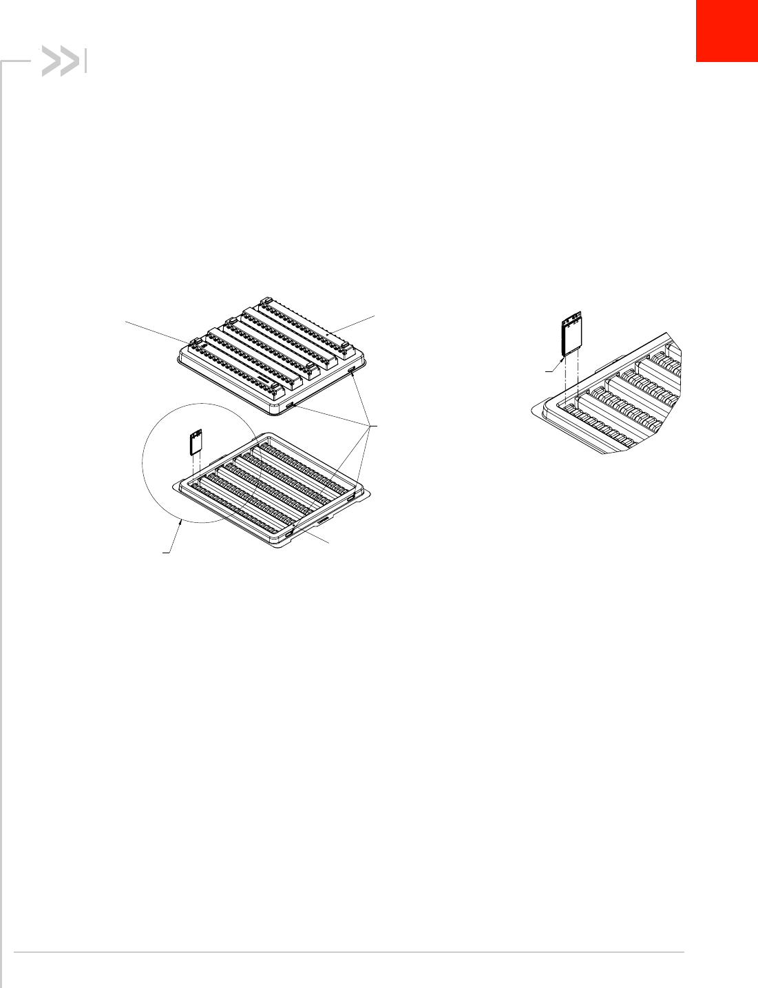
Rev 3 Sep.17 49 41110251
10
10: Packaging
Sierra Wireless AirPrime Mini Cards are packaged in sealed manufacturing boxes,
each containing a single tray with a capacity of 100 modules (Figure 10-1 and
Figure 10-2). Groups of three manufacturing boxes are then inserted into an outer
box for shipping (Figure 10-3).
In the standard packaging:
1. Mini Cards are inserted, system connector first, into the base portion (T1) of a
two-part tray. all facing the same direction. This allows the top edge of each Mini
Card to contact the top of the triangular features in the tray cover (T2) (see
Detail A).
2. The tray base and tray cover snap together at four connection points.
Figure 10-1: Device Placement in Module Tray
3. The tray cover (T2) is secured to the tray base (T1) with ESD-safe tape (EP1) at
four locations.
4. The tray is placed in a manufacturing box (T2 at the top), sealed with a security
tape (P1), and a manufacturing label (L3) is placed on the bottom-right corner,
above the security tape. If required for the SKU, an additional label (L4) can be
placed beside L3.
Triangular recesses
hold top edges of
Mini Cards
T2
Tray connection
points
See Detail A T1
System connector
Detail A
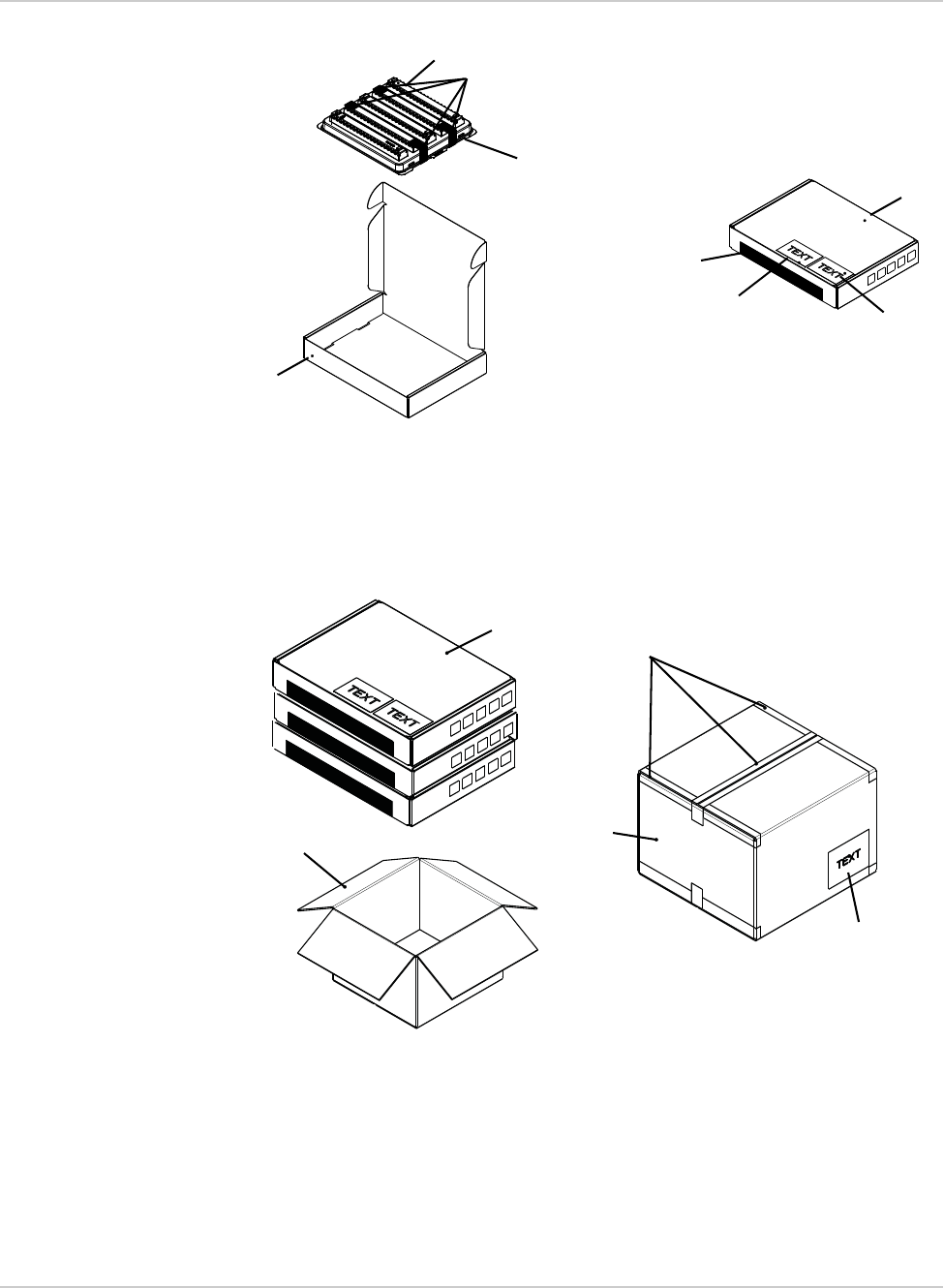
Product Technical Specification
Rev 3 Sep.17 50 41110251
Figure 10-2: Shipping Package
5. Three manufacturing boxes are placed in an outer shipping box (B2). If fewer
than three manufacturing boxes are being shipped, empty boxes are added to
the outer box
6. The outer box is sealed with security tape (P1) and a label (L5) is placed on
the box.
Figure 10-3: Outer (shipping) Box
T1
T2
EP1
B1
P1
L4
L3
B1
B1
B2 B2
P1
L5

Rev 3 Sep.17 51 41110251
11
11: References
This guide deals specifically with hardware integration issues that are unique to
AirPrime embedded modules.
Sierra Wireless Documents
For additional documents describing embedded module design, usage, and
integration issues, contact your Sierra Wireless account representative.
Command Documents
[1] AT Command Set for User Equipment (UE) (Release 6) (3GPP TS 27.007)
Industry/Other Documents
The following non-Sierra Wireless references are not included in your documentation
package:
[2] FCC Regulations - Part 15 - Radio Frequency Devices
[3] IEC-61000-4-2 level 3
[4] IEC-61000-4-2 level (Electrostatic Discharge Immunity Test)
[5] Mobile Station (MS) Conformance Specification; Part 4: Subscriber Interface
Module (Doc# 3GPP TS 11.10-4)
[6] PCI Express Mini Card Electromechanical Specification Revision 2.1
[7] Universal Serial Bus Specification, Rev 2.0
[8] JESD22-A114-B
[9] JESD22-C101
Rev 3 Sep.17 52 41110251
A
A: Acronyms
Table A-1: Acronyms and Definitions
Acronym or term Definition
3GPP 3rd Generation Partnership Project
8PSK Octagonal Phase Shift Keying
AGC Automatic Gain Control
API Application Programming Interface
BER Bit Error Rate—A measure of receive sensitivity
BLER Block Error Rate
bluetooth Wireless protocol for data exchange over short distances
CQI Channel Quality Indication
COM Communication port
CS Circuit-switched
CSG Closed Subscriber Group
CW Continuous waveform
dB Decibel = 10 x log10 (P1/P2)
P1 is calculated power; P2 is reference power
Decibel = 20 x log10 (V1/V2)
V1 is calculated voltage, V2 is reference voltage
dBm A logarithmic (base 10) measure of relative power (dB for decibels); relative to
milliwatts (m). A dBm value will be 30 units (1000 times) larger (less negative)
than a dBW value, because of the difference in scale (milliwatts vs. watts).
DC-HSPA+ Dual Carrier HSPA+
DCS Digital Cellular System
A cellular communication infrastructure that uses the 1.8 GHz radio spectrum.
DL Downlink (network to mobile)
DRX Discontinuous Reception
DSM Distributed Shared Memory
DUT Device Under Test
eICIC Enhanced Inter-Cell Interference Coordination
EIRP Effective (or Equivalent) Isotropic Radiated Power
EMC Electromagnetic Compatibility
EMI Electromagnetic Interference

Acronyms
Rev 3 Sep.17 53 41110251
ERP Effective Radiated Power
ESD Electrostatic Discharge
FCC Federal Communications Commission
The U.S. federal agency that is responsible for interstate and foreign
communications. The FCC regulates commercial and private radio spectrum
management, sets rates for communications services, determines standards for
equipment, and controls broadcast licensing. Consult www.fcc.gov.
FDD Frequency Division Duplexing
FDMA Frequency Division Multiple Access
feICIC Further Enhanced Inter-Cell Interference Coordination
FER Frame Error Rate—A measure of receive sensitivity.
firmware Software stored in ROM or EEPROM; essential programs that remain even when
the system is turned off. Firmware is easier to change than hardware but more
permanent than software stored on disk.
FOTA Firmware Over The Air—Technology used to download firmware upgrades
directly from the service provider, over the air.
FOV Field Of View
FSN Factory Serial Number—A unique serial number assigned to the mini card during
manufacturing.
GMSK Gaussian Minimum Shift Keying modulation
GPS Global Positioning System
An American system that uses a series of 24 satellites in middle circular orbit to
provide navigational data.
Host The device into which an embedded module is integrated
HSDPA High Speed Downlink Packet Access
HSPA+ Enhanced HSPA, as defined in 3GPP Release 7 and beyond
HSUPA High Speed Uplink Packet Access
Hz Hertz = 1 cycle/second
IF Intermediate Frequency
IMEI International Mobile Equipment Identity
IMS IP Multimedia Subsystem—Architectural framework for delivering IP multimedia
services.
inrush current Peak current drawn when a device is connected or powered on
inter-RAT Radio Access Technology
IOT Interoperability Testing
Table A-1: Acronyms and Definitions (Continued)
Acronym or term Definition

Product Technical Specification
Rev 3 Sep.17 54 41110251
IS Interim Standard.
After receiving industry consensus, the TIA forwards the standard to ANSI for
approval.
ISIM IMS Subscriber Identity Module (Also referred to as a SIM card)
LED Light Emitting Diode.
A semiconductor diode that emits visible or infrared light.
LHCP Left-Hand Circular Polarized
LNA Low Noise Amplifier
LPM Low Power Mode
LPT Line Print Terminal
LTE Long Term Evolution—a high-performance air interface for cellular mobile
communication systems.
MCS Modulation and Coding Scheme
MHz Megahertz = 10e6 Hz
NAS/AS Network Access Server
NC No Connect
NIC Network Interface Card
NLIC Non-Linear Interference Cancellation
NMEA National Marine Electronics Association
OEM Original Equipment Manufacturer—a company that manufactures a product and
sells it to a reseller.
OFDMA Orthogonal Frequency Division Multiple Access
OMA DM Open Mobile Alliance Device Management—A device management protocol.
OTA ‘Over the air’ (or radiated through the antenna)
PA Power Amplifier
packet A short, fixed-length block of data, including a header, that is transmitted as a unit
in a communications network.
PCB Printed Circuit Board
PCC Primary Component Carrier
PCS Personal Communication System
A cellular communication infrastructure that uses the 1.9 GHz radio spectrum.
PDN Packet Data Network
PMI Pre-coding Matrix Index
Table A-1: Acronyms and Definitions (Continued)
Acronym or term Definition

Acronyms
Rev 3 Sep.17 55 41110251
PSS Primary synchronisation signal
PST Product Support Tools
PTCRB PCS Type Certification Review Board
QAM Quadrature Amplitude Modulation.
This form of modulation uses amplitude, frequency, and phase to transfer data on
the carrier wave.
QOS Quality of Service
QPSK Quadrature Phase-Shift Keying
RAT Radio Access Technology
RF Radio Frequency
RI Ring Indicator
roaming A cellular subscriber is in an area where service is obtained from a cellular service
provider that is not the subscriber’s provider.
RSE Radiated Spurious Emissions
RSSI Received Signal Strength Indication
SCC Secondary Component Carrier
SDK Software Development Kit
SED Smart Error Detection
Sensitivity Measure of lowest power signal that the receiver can measure.
Sensitivity (RF) Measure of lowest power signal at the receiver input that can provide a prescribed
BER/BLER/SNR value at the receiver output.
SIB System Information Block
SIM Subscriber Identity Module. Also referred to as USIM or UICC.
SIMO Single Input Multiple Output—smart antenna technology that uses a single
antenna at the transmitter side and multiple antennas at the receiver side. This
improves performance and security.
SISO Single Input Single Output—antenna technology that uses a single antenna at
both the transmitter side and the receiver side.
SKU Stock Keeping Unit—identifies an inventory item: a unique code, consisting of
numbers or letters and numbers, assigned to a product by a retailer for purposes
of identification and inventory control.
S/N Signal-to-noise (ratio)
SNR Signal-to-Noise Ratio
SOF Start of Frame—A USB function.
Table A-1: Acronyms and Definitions (Continued)
Acronym or term Definition

Product Technical Specification
Rev 3 Sep.17 56 41110251
SSS Secondary synchronisation signal.
SUPL Secure User Plane Location
TDD Time Division Duplexing
TIA/EIA Telecommunications Industry Association / Electronics Industry Association.
A standards setting trade organization, whose members provide communications
and information technology products, systems, distribution services and
professional services in the United States and around the world. Consult
www.tiaonline.org.
TIS Total Isotropic Sensitivity
TRP Total Radiated Power
UDK Universal Development Kit (for PCI Express Mini Cards)
UE User Equipment
UICC Universal Integrated Circuit Card (Also referred to as a SIM card.)
UL Uplink (mobile to network)
UMTS Universal Mobile Telecommunications System
USB Universal Serial Bus
USIM Universal Subscriber Identity Module (UMTS)
VCC Supply voltage
VSWR Voltage Standing Wave Ratio
WAN Wide Area Network
WLAN Wireless Local Area Network
ZIF Zero Intermediate Frequency
ZUC ZUC stream cypher
Table A-1: Acronyms and Definitions (Continued)
Acronym or term Definition

Rev 3 Sep.17 57 41110251
Index
Numerics
3D gain, average
gain
3D average (GNSS), 45
3GPP compliance
LTE, 12
A
acronyms and definitions, 52– 56
antenna
connection considerations, 24
connectors, 13
custom, design, 25
GNSS, specifications, recommended, 45
limit, matching coaxial connections, 24
location, considerations, 25
matching, considerations, 25
maximum cable loss, 24
routing, 25
specification, 43– 46
specifications, recommended, 43
testing, 45
antennas
design checklist, 47
application interface features, 9
approvals, regulatory and industry, 40
averaged call mode DC power consumption, 31
averaged standby DC power consumption, 30
B
bands supported, RF
summary, 9
LTE, 28
bearers, dedicated, 10
block diagram
system, 13
bottom view, 35
C
cable loss
antenna, maximum, 24
capacitors
with SIM, 21
with XIM_DATA / XIM_CLK, 21
checklist, design, 47
communications, host to modem
design checklist, 48
conducted Tx power tolerances, 28
connection
grounding, 25
connectors, 24
connectors, required
host-module, 11
control interface, 22
CQI, 10
D
DC power consumption
averaged call mode, 31
averaged standby, 30
desense. See RF
design checklist
antennas, 47
component placement, 47
EMI/ESD, 47
host/modem communications, 48
power, 47
thermal, 48
USB3, 47
detach procedure, 10
digital interface, 23
dimensioned view, 35
dimensions, 34, 35
diversity connector, location, 24
drop specifications, 34
E
EDGE
connector, required, 11
electrical specifications, 13
electrostatic discharge. See ESD
envelope correlation coefficient, 44
environmental specifications, 34– 36
ESD
design checklist, 47
protection requirements, 36
F
field of view, 45
filtering, RF desense, 27
form factor, 34
FOV, 45
free space average gain, 45
frequencies supported, 28
frequency band support
LTE, 28

Product Technical Specification
Rev 3 Sep.17 58 41110251
G
gain
GNSS, 45
maximum, 41, 44
mean effective, 44
mean effective imbalance, 44
GNSS
antenna specifications, recommended, 45
connector location, 24
features supported, 10
GPS
specifications, 29
ground specifications, 18
grounding
connection considerations, 25
H
host interface
pin assignments, 14
humidity specifications, 34
I
I/O connector location, 24
I/O rise time requirements, 21
impedance
module–antenna, 25
SIM, 21
industry approvals, 40
integration requirements, 11
interface
control interface, 22
digital interface, 23
feature summary, 9
host, pin assignments, 14
SIM, 19
USB, 18
interference
device generated, 26
host-generated, 26
power supply noise, 33
wireless devices, 26
intra-LTE mobility, 10
isolation, 44, 45
L
labeling, 36
LED
example, 23
LED output, 13, 22
LTE
3GPP compliance, 12
features, 10
frequency band support, 28
M
mean effective gain, 44
mean effective gain imbalance, 44
mechanical specifications, 34– 36
N
noise
leakage, minimizing, 25
RF interference, power supply, 33
O
OEM
labeling, 36
ordering information, 11
P
packaging, 49
paging procedures, 10
PCB
multi-layer, shielding for RF desense, 27
PDN connections, multiple, 10
pin assignments, host interface, 14
PMI, 10
polarization, 45
position location, 10
power
design checklist, 47
handling, 44
power-up timing, 31
ramp-up timing, 31
supply, RF interference, 33
supply, ripple limit, 33
power consumption, DC
averaged call mode, 31
averaged standby, 30
power specifications, 18
power tolerances, conducted Tx, 28
R
radiated efficiency, total, 44
radiated sensitivity measurement, 27
radiated spurious emissions, 27
radiation patterns, 44
references, 51
regulatory approvals, 40
regulatory information, 40– 42
FCC, 41
limitation of liability, 40
safety and hazards, 40
reset device, 23
resistors, external pull-up, 21

Index
Rev 3 Sep.17 59 41110251
RF
antenna cable loss, maximum, 24
antenna connection, considerations, 24
connectors, required, 11
desense
device-generated, 26
harmonic energy, filtering, 27
mitigation suggestions, 27
shielding suggestions, 27
interference
other devices, 26
power supply, 33
wireless devices, 26
RF bands supported
summary, 9
LTE, 28
RF connector location, 24
RF specifications, 24–??
RI, 10
RSE, 27
Rx sensitivity
conducted, 28
S
sales
ordering, 11
sensitivity
conducted, RF parameter, 28
defined, 28
radiated measurement, overview, 27
testing, overview, 27
shielding
module, compliance, 24
reducing RF desense, 27
shock specifications, 34
signals, 22
SYSTEM_RESET_N, 23
WAKE_N, 22
WLAN_LED_N, 22
SIM
capacitor recommendations, 21
card contacts, 20
clock rate, 21
connector, required, 11
electrical specifications, 21
impedance, connectors, 21
interface, 19
interface diagram, 20
operation, 21
specifications
electrical, 13
environmental specifications, 34– 36
GPS, 29
mechanical, 34– 36
RF, 24–??
standby DC power consumption, averaged, 30
system block diagram, 13
SYSTEM_RESET_N, 23
T
temperature specifications, 34
temperature, module. See thermal
thermal
considerations, 37– 38
design checklist, 48
dissipation, factors affecting, 37
dissipation, suggestions, 37
internal temperature, maximum, 38
testing, module, 38
timing
power ramp-up, 31
power-up, 31
top view, 35
tracking session
automatic, 10
standalone, 10
Tx power tolerances, conducted, 28
U
USB
high / full speed throughput performance, 18
interface, 18
USB3
design checklist, 47
V
vibration specifications, 34
VSWR, 43, 45
W
WAKE_N, 13, 22
WLAN_LED_N, 22