Sierra Wireless MC8765 Multi-Mode & Multi-Band Wireless Network MiniCard User Manual HW Integration Guide
Sierra Wireless Inc. Multi-Mode & Multi-Band Wireless Network MiniCard HW Integration Guide
Contents
- 1. User Manual
- 2. Regulatory section of user Manual
User Manual
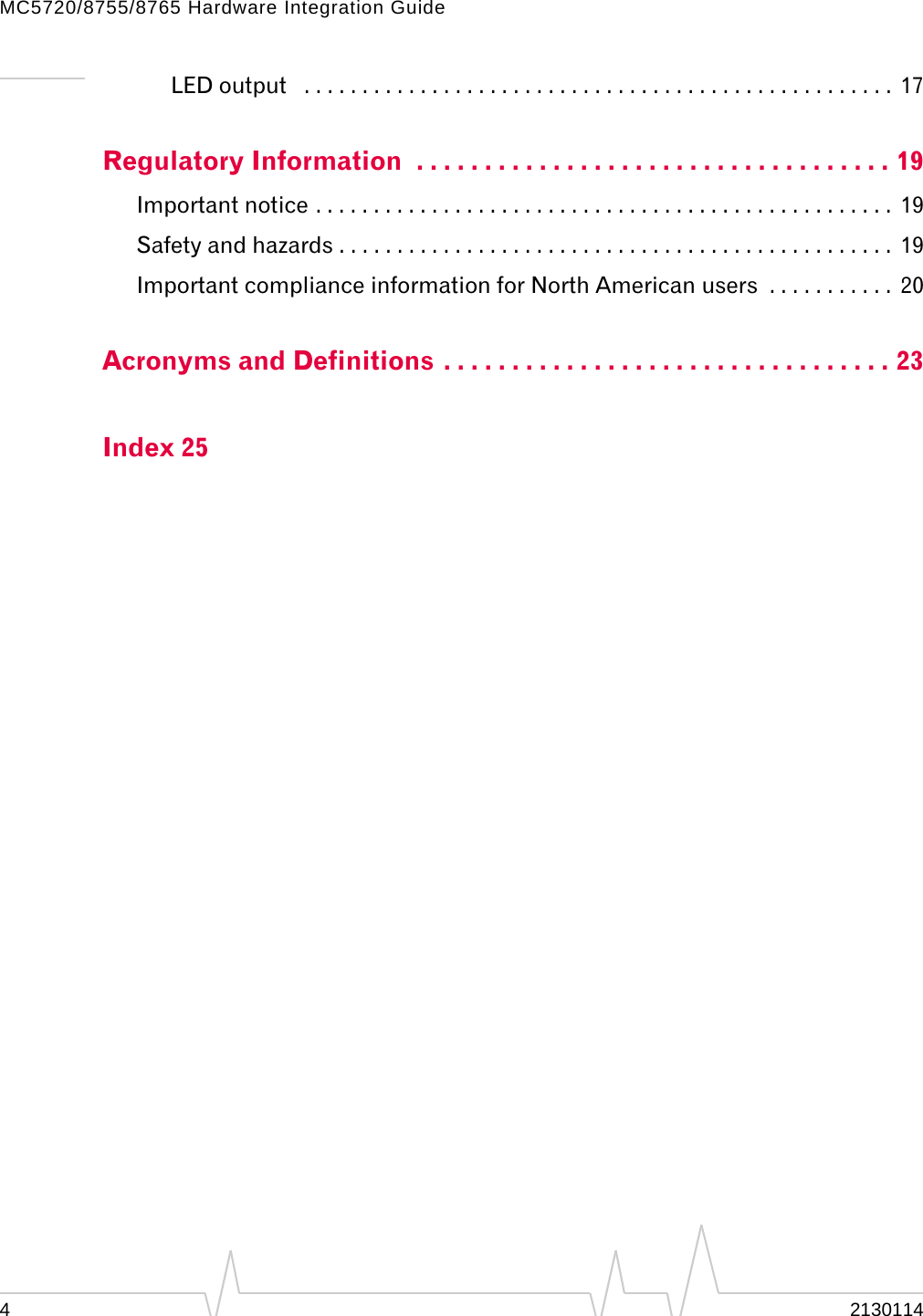

![Power Interface Rev 0.92 Nov.05 11 Normal state Note: This is the default state when VCC3.3 is first applied in the absence of W_Disable# control. This is the active state of the module. While in this state: • The module is fully powered. • The module is capable of placing/receiving calls or estab‐lishing data connections on the wireless network. • The USB interface is fully active. Low power mode In this power state, RF (both Rx and Tx) is disabled in the module, but the USB interface is still active. This low power mode (ʺairplane modeʺ) is controlled by a software command through the host interface. For instructions on using appropriate commands, refer to AT Command Set for User Equipment (UE) (Release 6) (+CFUN=0 command), EM5625/MC5720 CnS Reference (Document 2130643) (CNS_RADIO_POWER [0x1075]), or MC87xx Modem CnS Reference (Document 2130602) (Disable Modem). Usage models Usage models can be used to calculate expected current consumption. A sample usage model is provided in Table 2‐1. This example model applies to a battery‐operated device. In practice, because the module will be isolated from the battery (the host device manages the power source), the mAh ratings will depend on the device’s supply efficiency. Table 2-1: Power consumption of a sample application Used by a field worker (data only) Used for remote data logging Upload (module Tx) 1000 kB/day 40 kB/h Download (module Rx) 500 kB/day 100 kB/day Coverage / data rate 1X / 80 kbps IS-95 / 14.4 kbps Hours of operation 8 / day (off 16 hrs / day) 24 / day Total power consumed over 24 hours 60 mAh 200 mAh](https://usermanual.wiki/Sierra-Wireless/MC8765.User-Manual/User-Guide-608216-Page-13.png)