Sierra Wireless PCIE100 Cellular/ PCS CDMA Transmitter Module User Manual WM DEV PCIE100 UserGuide
Sierra Wireless, Inc. Cellular/ PCS CDMA Transmitter Module WM DEV PCIE100 UserGuide
UserManual.wiki
>
Sierra Wireless
>
PCIE100 User Manual
Users Guide
Navigation menu
Upload a User Manual
Namespaces
Wiki Guide
HTML
PDF
Info
Views
User Manual
Discussion / Help
Navigation
![PRELIMINARY WM_DEV_PCIE100_PTS_003 July, 01th 2008 confidential © Page : 8 / 37 This document is the sole and exclusive property of WAVECOM. Not to be distributed or divulged without prior written agreement. Ce document est la propriété exclusive de WAVECOM. Il ne peut être communiqué ou divulgué à des tiers sans son autorisation préalable. 1 References 1.1 References documents For more details, several references documents can be consulted. The WAVECOM reference documents are provided in the WAVECOM documents package contrary at the general reference documents which are not WAVECOM owner. 1.1.1 WAVECOM reference document 1.1.2 General reference document [1] PCI EXPRESS MINI CARD ELECTROMECHANICAL SPECIFICATION, REV 1.2 [2] USB2.0 standard](https://usermanual.wiki/Sierra-Wireless/PCIE100/User-Guide-993449-Page-8.png)
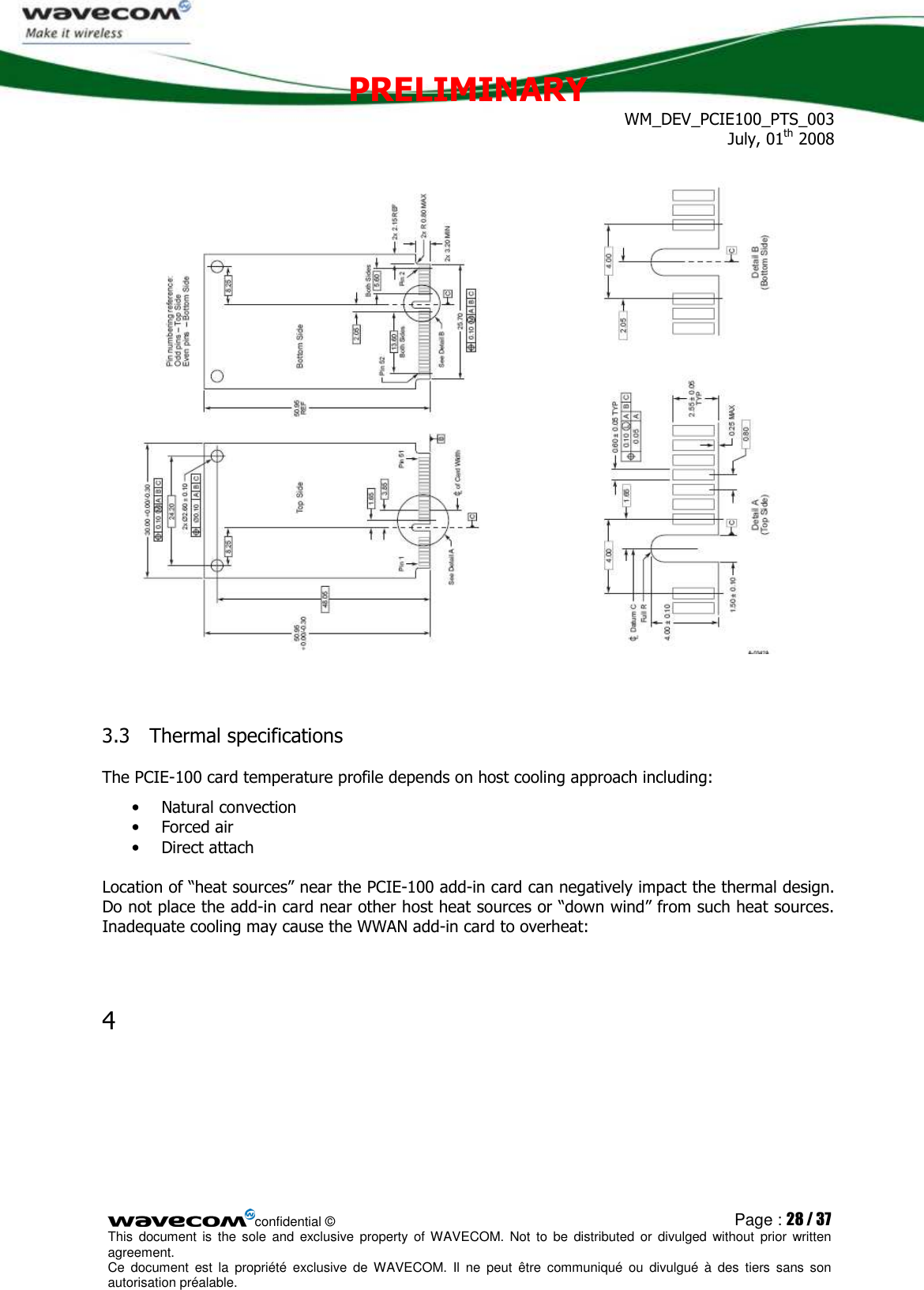
![PRELIMINARY WM_DEV_PCIE100_PTS_003 July, 01th 2008 confidential © Page : 27 / 37 This document is the sole and exclusive property of WAVECOM. Not to be distributed or divulged without prior written agreement. Ce document est la propriété exclusive de WAVECOM. Il ne peut être communiqué ou divulgué à des tiers sans son autorisation préalable. 3 Environmental Specifications 3.1 Temperature Range Wavecom specifies following temperature range PCIE-100 product Conditions Temperature range Operating / Class A -20 °C to +55°C Operating / Storage / Class B -40 °C to +85°C (TBC) Function Status Classification: Class A: The PCIE-100 shall have full function during and after an external influence. The GSM performance shall meet the minimum ETSI requirements. Class B: Any functions can be out of specified tolerances. All the functions will be going back to normal tolerances automatically after that the external influence has been removed. Performance is allowed to go outside of the minimum ETSI requirements, but it must be possible to connect a call and send an SMS. 3.2 Mechanical specifications PCIE-100 is fully compatible with Mini-PCI Express Standard as described in [1]. Standard connectors and latch up solutions could be used. 3.2.1 Mechanical drawings The next page gives main mechanical specifications of PCIE-100.](https://usermanual.wiki/Sierra-Wireless/PCIE100/User-Guide-993449-Page-27.png)
![PRELIMINARY WM_DEV_PCIE100_PTS_003 July, 01th 2008 confidential © Page : 29 / 37 This document is the sole and exclusive property of WAVECOM. Not to be distributed or divulged without prior written agreement. Ce document est la propriété exclusive de WAVECOM. Il ne peut être communiqué ou divulgué à des tiers sans son autorisation préalable. 5 This device complies with Part 15 of the FCC Rules. Operation is subject to the following two conditions: [1] this device may not cause harmful interference, and [2] This device must accept any interference received, including interference that may cause undesired operation. This equipment complies with FCC RF radiation exposure limits set forth for an uncontrolled environment. The antenna(s) used for this transmitter must be installed to provide a separation distance of at least 20 cm from all persons and must not be co-located or operating in conjunction with any other antenna or transmitter.” Maximum antenna gain that can be used with this product is 6.9dBi for 850MHz and 3.0dBi for 1900MHz.](https://usermanual.wiki/Sierra-Wireless/PCIE100/User-Guide-993449-Page-29.png)