Sierra Wireless Q2438 Dual-Band CDMA Wireless Module Evaluation Kit User Manual Starter Kit V2 User Guide
Sierra Wireless, Inc. Dual-Band CDMA Wireless Module Evaluation Kit Starter Kit V2 User Guide
Contents
- 1. Users Manual
- 2. Users Manual per CRN 10515
- 3. Raven and Pinpoint
- 4. Redwing
Users Manual

Starter Kit V2 User Guide
Reference: WI_HWD_SK_UGD_002
Level : 003
Date: 27 June 2003
confidential © Page : 1 / 17
This document is the sole and exclusive property of WAVECOM. Not to be distributed or divulged
without prior written agreement.
Ce document est la propriété exclusive de WAVECOM. Il ne peut être communiqué ou divulgué à
des tiers sans son autorisation préalable.

WM_HWD_SK_UGD_002 - 002
6/27/2003
Document Information
Level Date History of the evolution Writer
001 23/9/2002 First draft RNixon
002 24/9/2002 Mechanical drawings update RNixon
003 27/6/2003 Add PDF Schematic RNixon
Name Function Date Signature
Written by Russ Nixon Hardware Engineer 23/9/02
Checked by
Approved by
Distribution List
•
confidential © Page : 2 / 17
This document is the sole and exclusive property of WAVECOM. Not to be distributed or divulged
without prior written agreement.
Ce document est la propriété exclusive de WAVECOM. Il ne peut être communiqué ou divulgué à
des tiers sans son autorisation préalable.

WM_HWD_SK_UGD_002 - 002
6/27/2003
Contents
1 OVERVIEW............................................................................................................................................... 4
2 PRODUCT DESCRIPTION ..................................................................................................................... 5
3 DESCRIPTION OF THE INTERFACES ............................................................................................... 6
3.1 POWER.................................................................................................................................................. 6
3.2 COMPUTER ........................................................................................................................................... 6
3.2.1 DATA ........................................................................................................................................... 6
3.2.2 DM ............................................................................................................................................... 6
3.3 SWITCHES AND JUMPERS ...................................................................................................................... 7
3.3.1 ON/OFF Switch ........................................................................................................................... 7
3.3.2 BOOT Switch ............................................................................................................................... 7
3.3.3 RESET Switch .............................................................................................................................. 7
3.3.4 SNGL/DIFF Jumper .................................................................................................................... 7
3.4 AUDIO .................................................................................................................................................. 8
3.4.1 Handset........................................................................................................................................ 8
3.4.2 Headset ........................................................................................................................................ 8
3.5 RF ........................................................................................................................................................ 8
3.6 SIM SOCKET ........................................................................................................................................ 9
3.7 ADDITIONAL INTERFACES..................................................................................................................... 9
3.7.1 Vibrator........................................................................................................................................ 9
3.7.2 Ringer .......................................................................................................................................... 9
3.7.3 GPIO............................................................................................................................................ 9
3.7.4 Keypad ....................................................................................................................................... 10
3.7.5 JTAG.......................................................................................................................................... 10
3.8 LED FUNCTION .................................................................................................................................. 10
3.8.1 LED1.......................................................................................................................................... 11
3.8.2 LED2.......................................................................................................................................... 11
4 START-UP ............................................................................................................................................... 11
4.1 CONNECTIONS .................................................................................................................................... 11
4.2 CONFIGURATION................................................................................................................................. 12
4.2.1 Computer ................................................................................................................................... 12
4.2.2 Power Supply ............................................................................................................................. 12
4.2.3 Interface Board.......................................................................................................................... 12
5 TROUBLESHOOTING .......................................................................................................................... 13
5.1 NO RF SIGNAL.................................................................................................................................... 13
5.2 THE MODULE DOES NOT ANSWER THROUGH THE SERIAL LINK ........................................................... 13
5.3 NO AUDIO ........................................................................................................................................... 13
6 INTERFACE BOARD PHYSICAL DRAWINGS................................................................................ 13
6.1 LAYOUT.............................................................................................................................................. 13
6.2 ASSEMBLY DRAWING ......................................................................................................................... 15
6.3 ISOMETRIC .......................................................................................................................................... 16
6.4 SCHEMATIC ........................................................................................................................................ 17
confidential © Page : 3 / 17
This document is the sole and exclusive property of WAVECOM. Not to be distributed or divulged
without prior written agreement.
Ce document est la propriété exclusive de WAVECOM. Il ne peut être communiqué ou divulgué à
des tiers sans son autorisation préalable.

WM_HWD_SK_UGD_002 - 002
6/27/2003
1 Overview
This Document is intended to provide the user complete instructions on the
capabilities and use of the Wavecom Starter Kit. The Wavecom Starter Kit is
designed to allow the customer to interface to the Wavecom Q2300 and
Q2400 CDMA and GSM/GPRS Module families. Control of the Module is done
via AT Commands issued from an external PC running a terminal emulator,
such as HyperTerminal. The User should refer to the Wavecom
CDMA AT
Commands Interface Specification
for more information on supported
commands.
confidential © Page : 4 / 17
This document is the sole and exclusive property of WAVECOM. Not to be distributed or divulged
without prior written agreement.
Ce document est la propriété exclusive de WAVECOM. Il ne peut être communiqué ou divulgué à
des tiers sans son autorisation préalable.

WM_HWD_SK_UGD_002 - 002
6/27/2003
2 Product Description
The Wavecom Starter Kit includes the following:
Interface Board
The Interface Board provides a working platform for testing and evaluating the
performance of the Module, as well as allowing customer design of host
software interfaces.
Module
One Wavecom module is included with the Starter Kit and comes pre-
assembled on the Interface Board. The Module is soldered down via its four
Ground contact pins, and is also mated to the 60 pin board-to-board connector
of the Interface Board.
Handset
The Handset contains a standard telephony earpiece and microphone,
providing a full audio interface to the Module through the Interface Board
connectors.
Serial Cable
The Serial Cable connects the Interface Board to the controlling PC.
Antenna and RF Adapter
The Antenna provides sufficient omni-directional gain to allow the module to
go over the air on the network. An Antenna Adapter is provided to allow the
Antenna Cable to connect to the RF Connector of the Module.
Power Adapter
The included Power Adapter allows for use of the Starter Kit without the need
for a lab power supply. The Adapter can source enough current to support
CDMA, GSM, and GPRS modules at full transmit power, as well as the
operation of the Interface Board. Some Kits may include a lab power supply
cable instead of, or in addition to, the Power Adapter.
confidential © Page : 5 / 17
This document is the sole and exclusive property of WAVECOM. Not to be distributed or divulged
without prior written agreement.
Ce document est la propriété exclusive de WAVECOM. Il ne peut être communiqué ou divulgué à
des tiers sans son autorisation préalable.

WM_HWD_SK_UGD_002 - 002
6/27/2003
3 Description of the Interfaces
3.1 Power
A standard DC Power Jack is provided on the Interface Board. The included
Power Adapter can be used to supply the Module and Interface Board via this
jack.
Alternatively a lab power supply capable of supplying at least 3.8Vdc at
2.0Amps can be used. The advantage of the lab power supply is in allowing
the user to monitor the current drain of the Module to help determine its
operating state.
The Power Jack has a center positive connection, if a lab supply or other
external source is used. A cable for this purpose is available.
3.2 Computer
The Interface Board communicates with the controlling PC through standard
RS-232 Interfaces. Two such interfaces are provided, however the typical
customer application will only require one of these (DATA).
3.2.1 DATA
The DATA Interface, J200, provides a full 8 wire RS-232 interface with the PC.
This interface supports the AT Commands; the Diagnostic (DM) information;
and high speed data.
Light Emitting Diodes (LEDs) for this port are included on the Interface Board
on the RX, TX, DTR, DSR, RTS, CTS and DCD lines to indicate the state of the
line. The red LED indicates a negative voltage on the RS-232 (Logic 1) and the
green LED indicates a positive voltage on the RS-232 (Logic 0).
3.2.2 DM
The DM Interface, J201, provides a 2 wire RS-232 interface for Diagnostic
information only. The typical customer application should not require this
interface as all functionality of the DM Interface is now supported through the
DATA Interface as well.
Light Emitting Diodes (LEDs) for this port are included on the Interface Board
on both the RX and TX lines to indicate the state of the line. The red LED
indicates a negative voltage on the RS-232 (Logic 1) and the green LED
indicates a positive voltage on the RS-232 (Logic 0).
confidential © Page : 6 / 17
This document is the sole and exclusive property of WAVECOM. Not to be distributed or divulged
without prior written agreement.
Ce document est la propriété exclusive de WAVECOM. Il ne peut être communiqué ou divulgué à
des tiers sans son autorisation préalable.

WM_HWD_SK_UGD_002 - 002
6/27/2003
3.3 Switches and Jumpers
3.3.1 ON/OFF Switch
There is a slide switch, SW101, located on the back edge of the Interface
Board. This switch interfaces directly to the ON/OFF control line of the
Module, via pin 6 of the board-to-board connector. Sliding the switch in the
“OFF” direction will pull the line low, causing the Module to shut off. Sliding
the switch in the “ON” direction will pull the line high, turning on the Module
and keeping it in the ON state.
3.3.2 BOOT Switch
A second slide switch, SW102, is located on the back edge of the Interface
Board, beside the ON/OFF switch. The function of this switch depends on if a
CDMA Module or GSM/GPRS Module is being used.
For normal operation of the GSM Module, this switch must be in the HI
position upon power up or reset. This switch when in the LO position will put
the GSM Module into its BOOT Mode. This allows software upgrades to the
embedded code within the Module, via the serial interface of the Interface
Board and an application such as the Wavecom DWLWin program. Note that
the switch must be in the LO state upon power up or reset. Once the
embedded code is executing, the status of the BOOT input is no longer
monitored.
For the CDMA Modules, there is no need for this BOOT functionality. Thus
this switch is for test purposes only and is connected to GPIO 42 of the
Module. The input can be pulled LO or HI and monitored via AT Command
Queries if needed.
3.3.3 RESET Switch
There is a master push button reset switch, SW100, located in the middle of
the Interface Board that when depressed will pull the RESET/ line of the
Module to Ground, causing a full Module microprocessor reset.
3.3.4 SNGL/DIFF Jumper
A four-pin jumper, J303, is located near the Audio connectors. This is used to
configure the Headset Audio for either a single ended or differential speaker
drive circuit. Silkscreen on the Interface Board indicates the jumper positions
required for either case. For Differential, one jumper should be placed across
pins 2 and 3. For Single Ended, two jumpers should be placed; one across
pins 1 and 2, and the other across pins 3 and 4. Refer to
Audio
for more
details on the functionality of this jumper block.
confidential © Page : 7 / 17
This document is the sole and exclusive property of WAVECOM. Not to be distributed or divulged
without prior written agreement.
Ce document est la propriété exclusive de WAVECOM. Il ne peut être communiqué ou divulgué à
des tiers sans son autorisation préalable.

WM_HWD_SK_UGD_002 - 002
6/27/2003
3.4 Audio
There are two unique audio paths provided for on the Interface Board, and
supported by the Module.
3.4.1 Handset
The Handset Jack (J300) supports fully differential microphone and speaker
signals. The microphone is also biased and filtered on the Interface Board.
The Handset included in the Starter Kit can be used with this port.
This Handset audio path is considered Path 1 in the AT Command Set.
3.4.2 Headset
The Headset Jack (J301) supports a biased differential microphone however
the speaker path is either single or differential for GSM/GPRS or single ended
only for CDMA. This difference is due to limitations of the CDMA design,
allowing for only one fully differential speaker path. Jumpers on J303
configure the path for single (SNGL) or differential (DIFF) audio. The Handset
included in the Starter Kit can be used with this port.
There is an additional audio jack included on the Interface Board that supports
the use of a standard 2.5mm three-wire cell phone headset (not included).
This jack (J302) supports only single ended microphone and speaker signals,
and is wired in parallel with the Headset Jack, J301. Only J301 or J302 can
be used at once, and the jumpers on J303 must be set for single ended
operation to use J302. Note the single ended audio does result in an increased
noise floor, especially when the Starter Kit is used with a GSM or GPRS
Module. Careful filtering and attention to layout is required in a customer
application to minimize this noise.
These Headset audio paths are considered Path 0 in the AT Command Set.
3.5 RF
There are two RF connection points on the Interface Board, both used to
provide an RF path from the Module to the Interface Board mounted RF jack.
The Module will be supplied with an RF “pigtail” cable assembly. This pigtail
is soldered to the module and terminates in a bulkhead style RF SMA
connector. This can be mounted on the Interface Board through the ground
ring labeled “RF”, and the supplied Antenna screwed onto this connector. This
is the preferred method of connecting the RF Antenna.
Alternatively, under the Module there are pads where an optional surface
mount connector can be soldered that will mate with similar pads on the
confidential © Page : 8 / 17
This document is the sole and exclusive property of WAVECOM. Not to be distributed or divulged
without prior written agreement.
Ce document est la propriété exclusive de WAVECOM. Il ne peut être communiqué ou divulgué à
des tiers sans son autorisation préalable.

WM_HWD_SK_UGD_002 - 002
6/27/2003
Module. A connector such as the Radiall R107.064.000 is suggested (see Note
below). The RF signal would then be passed to J500, which supports a
connector such as the AMP/TYCO 221790-1 Right Angle PCB Mount SMA
Connector (not included). The Antenna included in the Starter Kit can attach to
this jack.
Note: The Radiall connector has not been fully tested or characterized for
either CDMA or GSM/GPRS. It is not recommended for customer testing or
customer use in a final design. Some versions of the Module may not support
the use of a surface mount RF connector.
3.6 SIM Socket
The SIM socket is provided for use with the RUIM (CDMA) or SIM (GSM/GPRS)
card. The Interface Board supports the low voltage cards, having a supply of
2.8Vdc from the Module. The RUIM card is not yet required for North
American CDMA modules.
3.7 Additional Interfaces
3.7.1 Vibrator
The Interface Board includes vibrator driver circuitry that will allow the
customer to plug in an optional external vibration motor for testing. The
connection is made via test points TP500. A standard 1.6V to 3.0V cell phone
vibration motor can be used.
Alternatively, for test purposes a red LED has been added to indicate the state
of the line, and is located near the “VIBRA” label on the board.
3.7.2 Ringer
The Interface Board includes ringer driver circuitry that will allow the customer
to plug in an optional external buzzer/ringer for testing. The connection is
made via test points TP501. A standard 2.0V to 3.0V cell phone ringer can be
used.
Alternatively, for test purposes a green LED has been added to indicate the
state of the line, and is located near the “RINGER” label on the board.
3.7.3 GPIO
Included in the design are Test Points to allow the customer to access all
unused General Purpose Input/Outputs (GPIOs) provided by the Module.
These are direct from the Module, with no circuitry added. They are located
next to the Reset switch in the middle of the Interface Board, and are labeled
confidential © Page : 9 / 17
This document is the sole and exclusive property of WAVECOM. Not to be distributed or divulged
without prior written agreement.
Ce document est la propriété exclusive de WAVECOM. Il ne peut être communiqué ou divulgué à
des tiers sans son autorisation préalable.

WM_HWD_SK_UGD_002 - 002
6/27/2003
according to the CDMA Module schematic pin name. Two of these lines are
Analog to Digital inputs to the Module microprocessor, if required for testing.
Note that for the GSM Module design, the test point names do not apply and
the user will have to refer to the GSM schematic to determine the correct test
point location for a given line.
3.7.4 Keypad
For testing purposes, an optional keypad can be installed on the Interface
Board that will provide the customer a 5x4 matrix of keys for test and debug.
The keypad should be a Grayhill 88JB2 and can be purchased in North
America through Digikey with a GH5020-ND part number. The Module itself
can support a bigger matrix, however the keypad chosen was the largest
standard keypad that could be found.
Note that for the CDMA Module, the JTAG and Keypad share the same Module
interface pins thus cannot be used at the same time. Additionally, the CDMA
Module itself requires a different hardware population to implement each path.
The default population configuration for the CDMA module enables the
Keypad, not the JTAG Interface.
3.7.5 JTAG
Included on the Interface Board for debugging purposes is a JTAG Header
(J202). The connector, when needed, should be soldered to the bottom side of
the Interface Board. This connector will not be required in a customer
application, and is therefore not normally populated on the board.
Note that only the CDMA Module supports a JTAG interface. The JTAG and
Keypad Interfaces share the same Module interface pins thus cannot be used
at the same time. Additionally, the CDMA Module itself requires a different
hardware population to implement each path. The default population
configuration for the CDMA module enables the Keypad, not the JTAG
Interface.
3.8 LED Function
There are two general status indicators, LED1 and LED2, on the Interface
Board. The drive circuits for these are controlled directly from the Module, via
the 60 pin board-to-board connector. Both LEDs are located near the Power
Jack on the Interface Board.
Additional indicators are included for the Vibrator and Ringer driver circuits,
and for the DM and DATA Interface ports. Refer to these headings for more
details of their function.
confidential © Page : 10 / 17
This document is the sole and exclusive property of WAVECOM. Not to be distributed or divulged
without prior written agreement.
Ce document est la propriété exclusive de WAVECOM. Il ne peut être communiqué ou divulgué à
des tiers sans son autorisation préalable.

WM_HWD_SK_UGD_002 - 002
6/27/2003
3.8.1 LED1
This LED is red when illuminated, and provides the user with an indication of
the Module status according to the following table:
LED1 Status Module Status
OFF In download mode or OFF
ON: Permanent ON but not registered on a
network
ON: Slow Flash
- 200mS ON, 2S OFF
ON and registered on a
network
ON: Quick Flash
- 200mS ON, 600mS
OFF
ON, registered on a network
and communication in progress
3.8.2 LED2
This LED is green when illuminated. The functionality of this LED can be
defined to provide a method of test and debug by the user via AT Commands.
It is connected via pin 54 of the board-to-board connector and is driven by
GPIO 8 on the CDMA Modules, and GPIO 4 on the GSM/GPRS Modules.
4 Start-up
The following gives a description of the connections and configurations
required to bring up the Module. Be sure to consider these recommendations
before applying power to the Interface Board and Module.
4.1 Connections
Be sure the Module is securely seated on the Interface Board, and the board-
to-board connector is correctly aligned. Ideally, the four grounding feet of the
Module should be soldered to the Interface Board from the bottom side. If the
Module is not soldered, an additional grounding clip may be required to
provide uninterrupted ground to the Module. Attach the Antenna, via the
Antenna Adapter, to the Module’s RF Cable.
Connect a serial cable to the DATA Connector on the Interface Board and to an
unused port on the controlling PC.
Plug the Power Adapter into wall outlet (or alternate Power Supply Cable and
lab power supply). Plug the round jack into Power Connector on the Interface
Board.
confidential © Page : 11 / 17
This document is the sole and exclusive property of WAVECOM. Not to be distributed or divulged
without prior written agreement.
Ce document est la propriété exclusive de WAVECOM. Il ne peut être communiqué ou divulgué à
des tiers sans son autorisation préalable.

WM_HWD_SK_UGD_002 - 002
6/27/2003
Insert the Handset Cable into the Handset and into whichever Audio Jack,
Headset or Handset, is to be used.
In the case of the GSM/GPRS Module, or the CDMA module requiring an R-
UIM, be sure to install the SIM/R-UIM into the socket provided.
4.2 Configuration
4.2.1 Computer
Control of the Module is via AT Commands issued from the PC running a
terminal emulator, such as HyperTerminal. Configure the PC serial port as
shown below:
Bits per second
Data Bits
Stop Bits
Flow control
115200/9200
8
1
Hardware
NOTE: 115200 is the default for CDMA. 9200 is the default for GSM.
4.2.2 Power Supply
The Power Adapter supplies 4.0 Volts DC and a maximum of 2.0 Amps. It can
be plugged into a 110 Volt or 220 Volt Mains input.
If a lab power supply is used instead, it should be set for 3.8 Volts DC with a
minimum current limit of 2.0 Amps.
4.2.3 Interface Board
Install the SNGL/DIFF Jumper as desired. Refer to the details above under
SNGL/DIFF Jumper
. The OFF/ON switch can be in either position when power
is applied, but will have to be moved to the ON position after the power is
applied in order to activate the module. The BOOT switch should be left in the
HI position for normal operation of the GSM/GPRS Module. For CDMA
Modules, the state of this switch is not critical.
confidential © Page : 12 / 17
This document is the sole and exclusive property of WAVECOM. Not to be distributed or divulged
without prior written agreement.
Ce document est la propriété exclusive de WAVECOM. Il ne peut être communiqué ou divulgué à
des tiers sans son autorisation préalable.

WM_HWD_SK_UGD_002 - 002
6/27/2003
5 Troubleshooting
5.1 No RF signal
• Verify the Antenna is correctly connected to the Module. Verify the
position of the Antenna is in a strong signal location.
5.2 The Module does not answer through the serial link
• No or incorrect power is being supplied to the Module. Verify the Power
Supply and ON/OFF Switch position.
• The Module is not adequately assembled onto the Interface Board.
Verify that proper grounding (ideally solder) is provided.
• The wrong DB-9 connector is being used. Verify that the DATA Port is
connected to the controlling PC.
• The terminal emulator application, HyperTerminal for example, is not
correctly configured for the Module. Verify the Baud rate. It is possible
that the Module has been configured for a different default Baud rate, so
it may be necessary to try different rates in HyperTerminal.
5.3 No audio
• The wrong Audio Path has been selected. Try the other Audio Jack, or
issue the AT Command to verify/select the correct path.
• The SNGL/DIFF Jumper is not correctly installed. This only affects the
Headset Audio Path.
6 Interface Board Physical Drawings
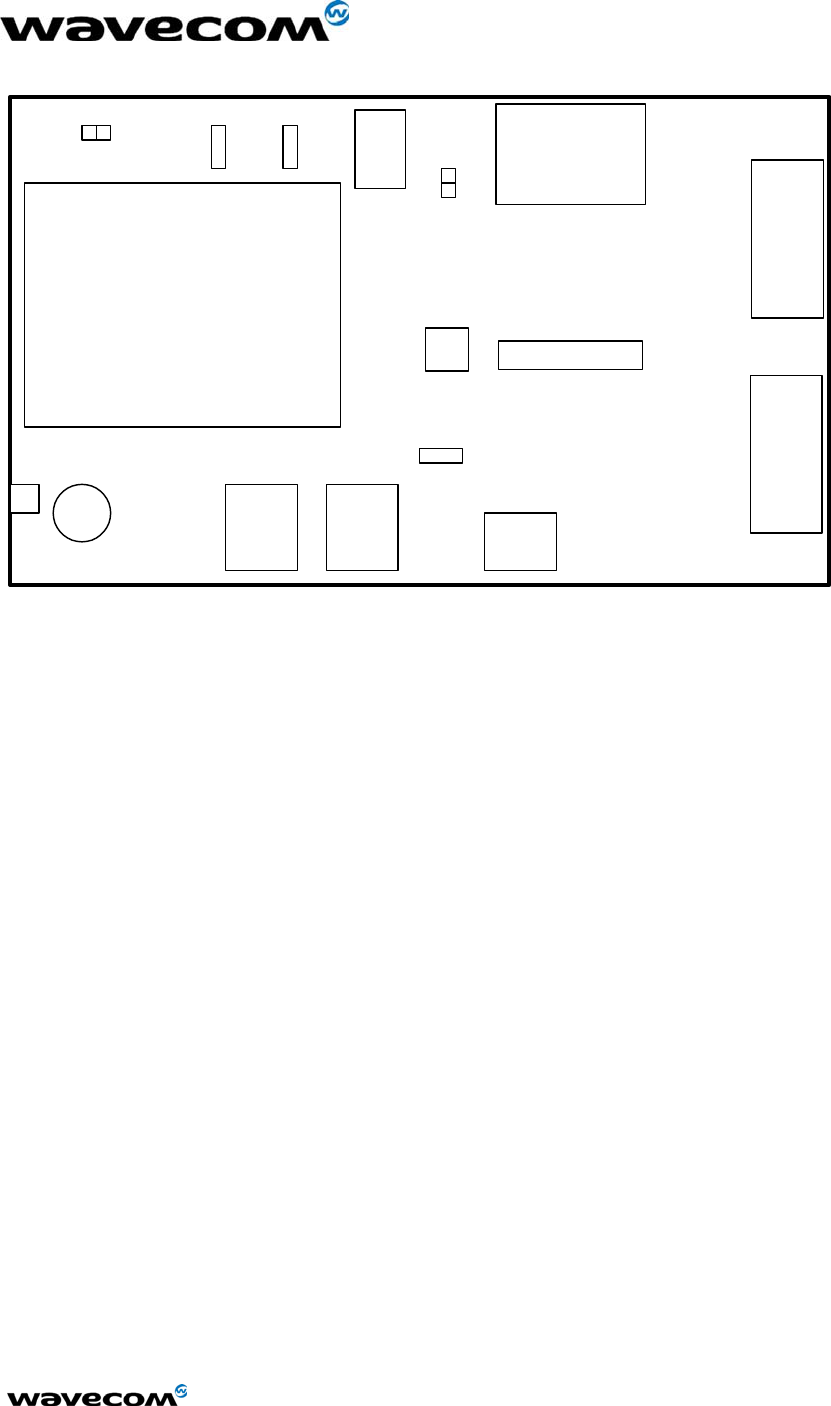
6.1 Layout
The following drawing indicates the relative position of all switches,
connectors, and jumpers on the Interface Board, by functional name.
confidential © Page : 13 / 17
This document is the sole and exclusive property of WAVECOM. Not to be distributed or divulged
without prior written agreement.
Ce document est la propriété exclusive de WAVECOM. Il ne peut être communiqué ou divulgué à
des tiers sans son autorisation préalable.
WM_HWD_SK_UGD_002 - 002
6/27/2003
MODULE
DM
DB-9
DATA
DB-9
SIM
SOCKET
RF HEADSET HANDSET
HEADSET
JTAG
POWER
INPUT
RESET
SNGL/DIFF
LED 1
VIBRARINGER
OFF/ON
BOOT
LED 2
confidential © Page : 14 / 17
This document is the sole and exclusive property of WAVECOM. Not to be distributed or divulged
without prior written agreement.
Ce document est la propriété exclusive de WAVECOM. Il ne peut être communiqué ou divulgué à
des tiers sans son autorisation préalable.
WM_HWD_SK_UGD_002 - 002
6/27/2003
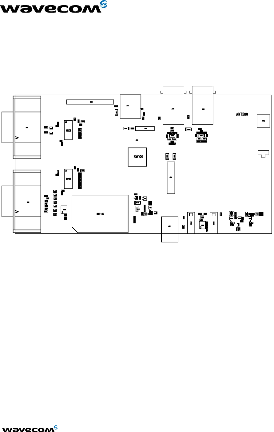
6.2 Assembly Drawing
The following drawing indicates the position of all components on the Interface
Board by schematic reference designator.
confidential © Page : 15 / 17
This document is the sole and exclusive property of WAVECOM. Not to be distributed or divulged
without prior written agreement.
Ce document est la propriété exclusive de WAVECOM. Il ne peut être communiqué ou divulgué à
des tiers sans son autorisation préalable.
WM_HWD_SK_UGD_002 - 002
6/27/2003
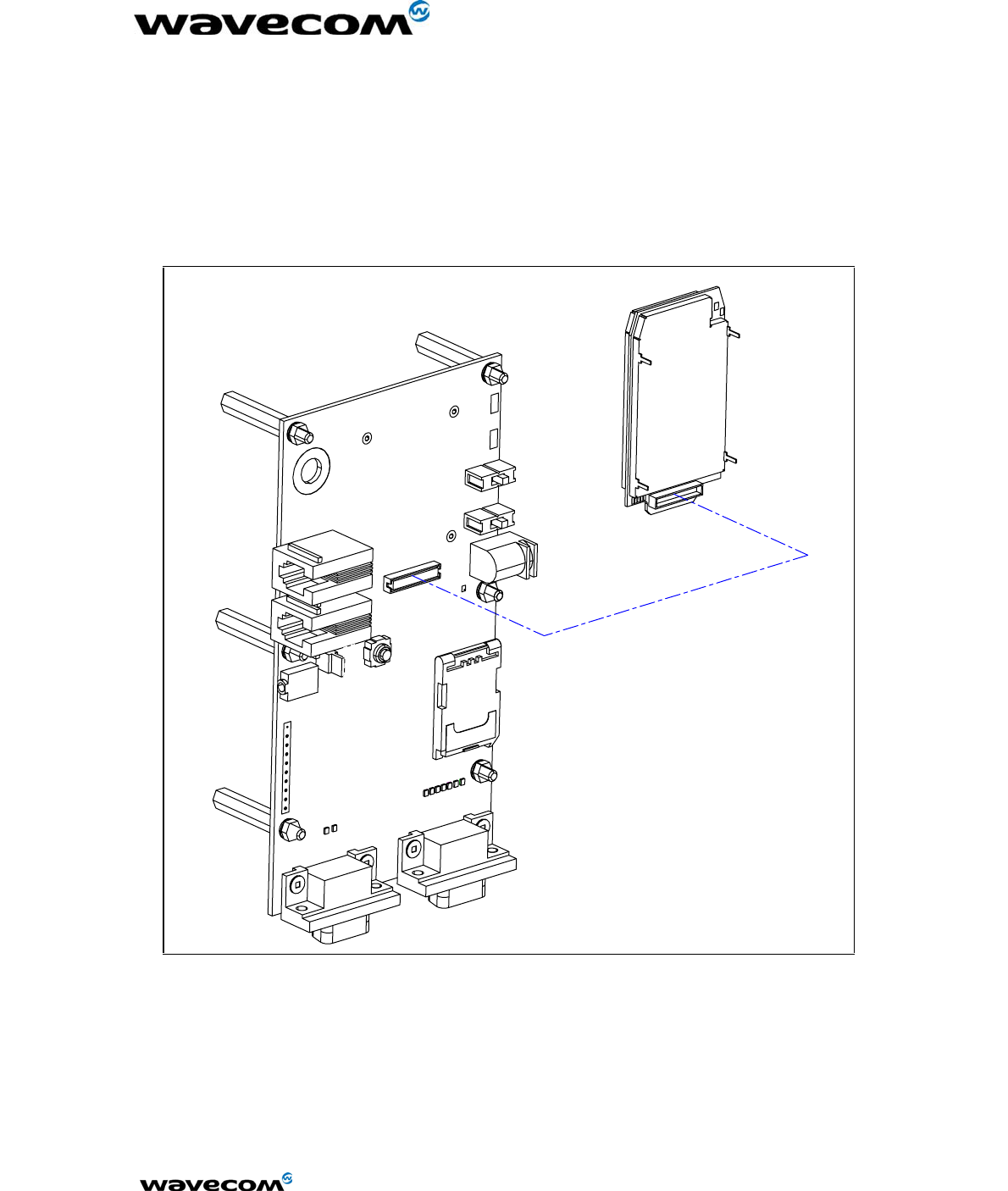
6.3 Isometric
The following drawing is an Isometric drawing of the Interface Board including
the Module.
confidential © Page : 16 / 17
This document is the sole and exclusive property of WAVECOM. Not to be distributed or divulged
without prior written agreement.
Ce document est la propriété exclusive de WAVECOM. Il ne peut être communiqué ou divulgué à
des tiers sans son autorisation préalable.

WM_HWD_SK_UGD_002 - 002
6/27/2003
confidential © Page : 17 / 17
This document is the sole and exclusive property of WAVECOM. Not to be distributed or divulged
without prior written agreement.
Ce document est la propriété exclusive de WAVECOM. Il ne peut être communiqué ou divulgué à
des tiers sans son autorisation préalable.
6.4 Schematic
The following pages are a PDF conversion of the Starter Kit schematic. Note
that the pages are not included in the overall page count of this document.
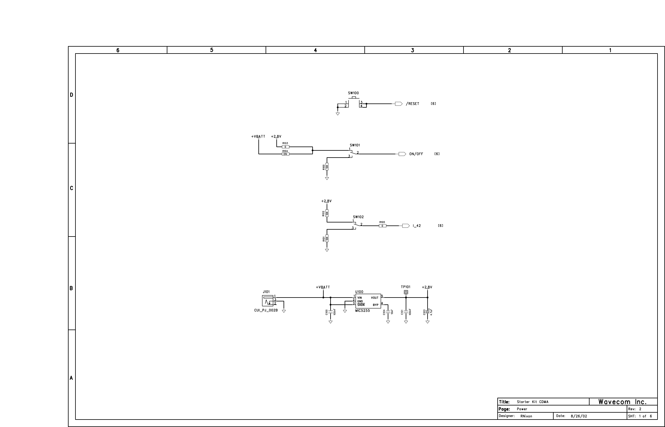
SKit_CDMA2-r10eco1.sch-1 - Fri Jun 27 12:02:53 2003
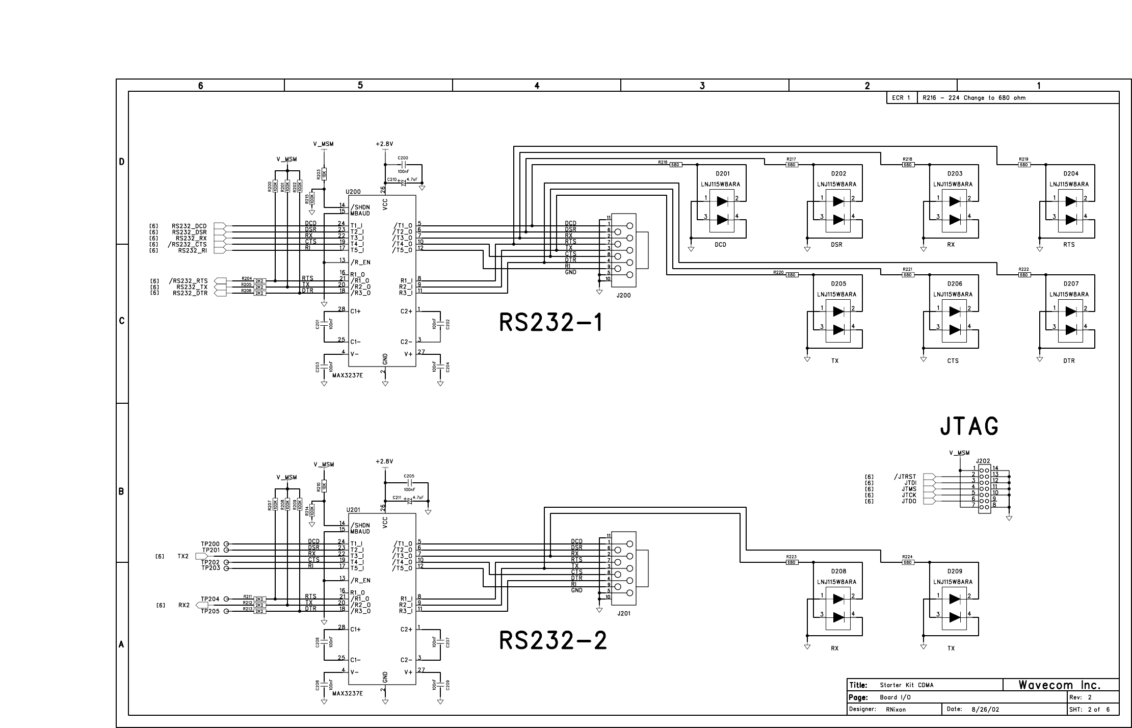
SKit_CDMA2-r10eco1.sch-2 - Fri Jun 27 12:02:54 2003
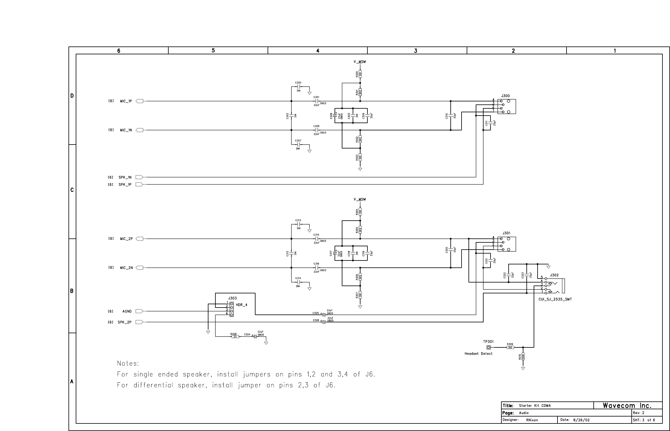
SKit_CDMA2-r10eco1.sch-3 - Fri Jun 27 12:03:00 2003
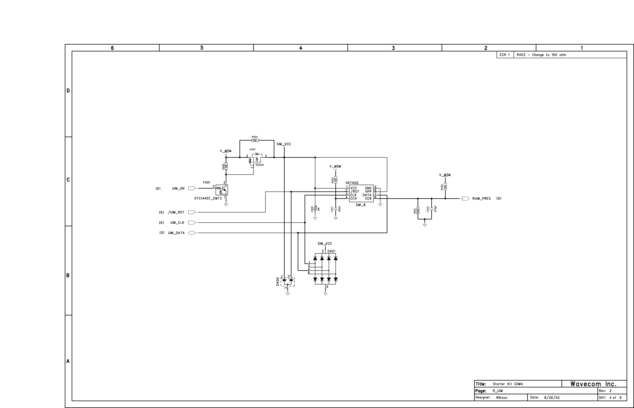
SKit_CDMA2-r10eco1.sch-4 - Fri Jun 27 12:03:01 2003
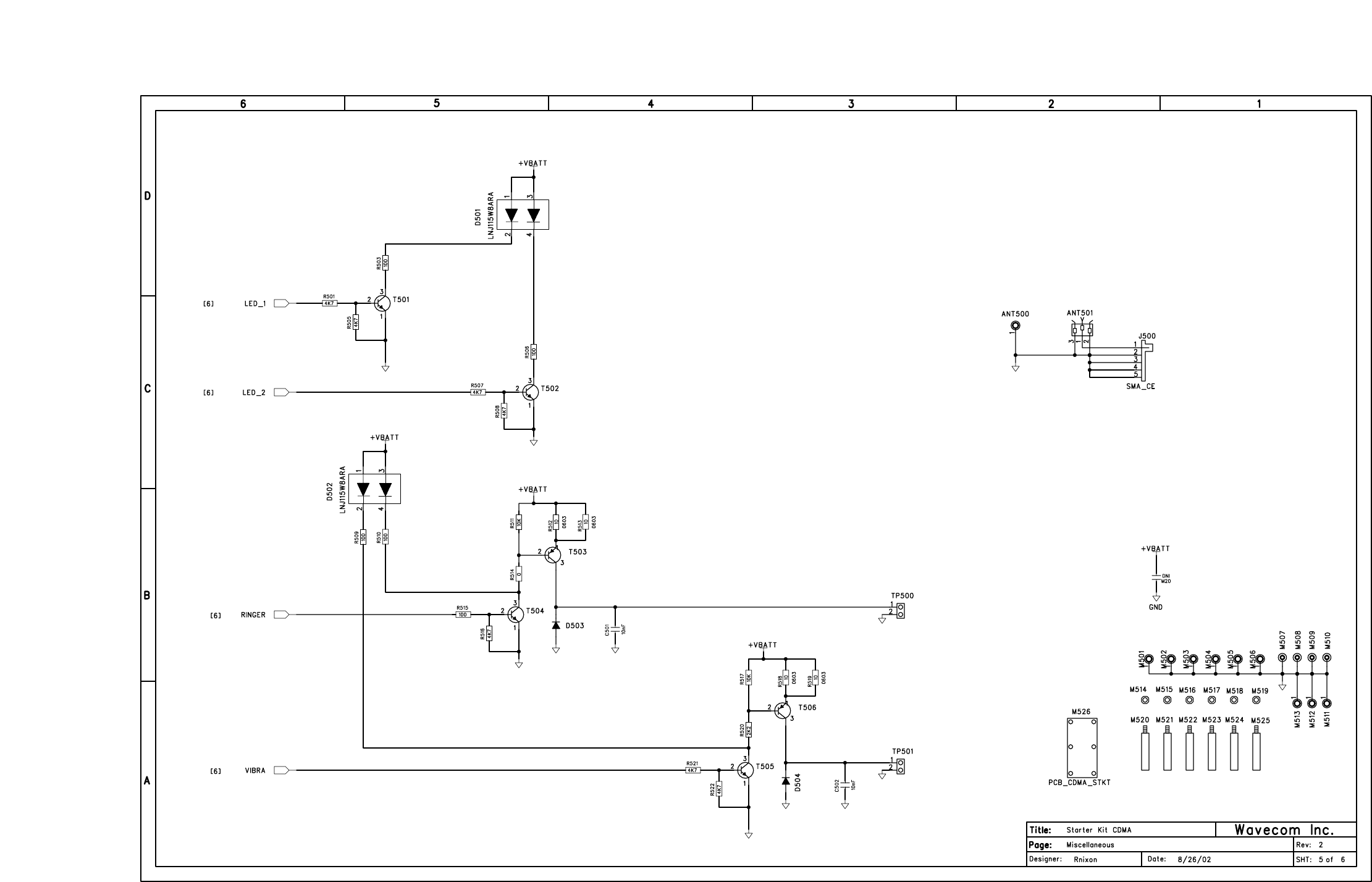
SKit_CDMA2-r10eco1.sch-5 - Fri Jun 27 12:03:01 2003
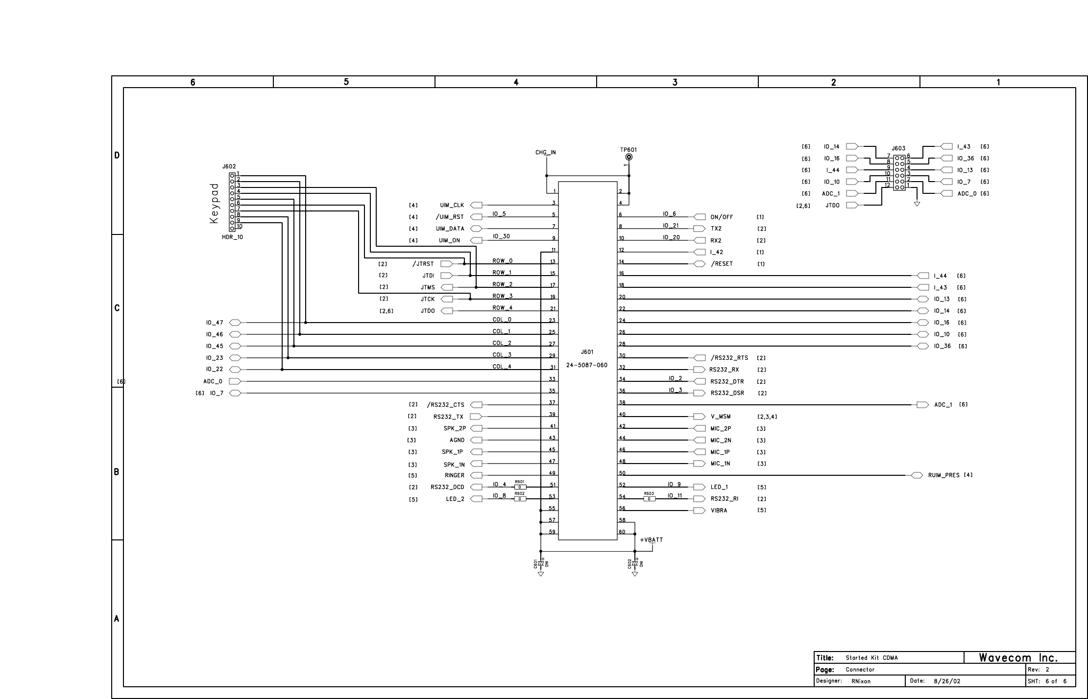
SKit_CDMA2-r10eco1.sch-6 - Fri Jun 27 12:03:02 2003