Sierra Wireless Q24EX001 Wireless CPU User Manual Wireless CPU Q24 Series
Sierra Wireless, Inc. Wireless CPU Wireless CPU Q24 Series
UserManual.wiki
>
Sierra Wireless
>
Q24EX001 User Manual
Users Manual
Navigation menu
Upload a User Manual
Namespaces
Wiki Guide
HTML
PDF
Info
Views
User Manual
Discussion / Help
Navigation

![Wireless CPU Q24 Series confidential © Page: 4 / 81 This document is the sole and exclusive property of WAVECOM. Not to be distributed or divulged without prior written agreement. WM_PRJ_Q24NG_PTS_001-003 November 2006 Overview This Product Specification document defines and specifies the Wireless CPU Q24 Series is available in four different GSM/GPRS Class 10 quad-band versions: • Q24 Classic: EGSM 900/1800/850/1900 MHz version with 32 Mb of Flash memory and 16 Mb of PSRAM (32/16), T° range [-20°C / +55°C]. • Q24 Plus: EGSM/GPRS 900/1800/850/1900 MHz version with 32 Mb of Flash memory and 16 Mb of PSRAM (32/16), T° range [-20°C / +55°C]. • Q24 Extended: EGSM/GPRS 900/1800/850/1900 MHz version with 32 Mb of Flash memory and 4 Mb of SRAM (32/4), extended T° range. • Q24 Automotive: EGSM/GPRS 900/1800/850/1900 MHz version with 32 Mb of Flash memory and 4 Mb of PSRAM (32/4), extended T° range. This version is dedicated to automotive applications. This document covers the Wireless CPU alone and do not include the programmable capabilities provided in Open AT® Software Suites. For detailed software programming guides, refer to the documents shown in the "Reference documents" section. Open AT® Software Suites allow developers to natively execute ANSI C software programs directly on the Wireless CPU.](https://usermanual.wiki/Sierra-Wireless/Q24EX001/User-Guide-734426-Page-5.png)
![Wireless CPU Q24 Series References ©Confidential Page: 10 / 81 This document is the sole and exclusive property of WAVECOM. Not to be distributed or divulged without prior written agreement. WM_PRJ_Q24NG_PTS_001-003 November 2006 1 References 1.1 Reference Documents For more details, several reference documents may be consulted. The Wavecom reference documents are provided in the Wavecom documents package contrary to the general reference documents, which are not Wavecom owned. 1.1.1 Wavecom Reference Documents [1] Automotive Environmental Control Plan for Wireless CPU Q24 Series WM_PRJ_Q24NG_DCP_001 [2] Environmental Control Plan for Wireless CPU Q24 Series WM_PRJ_Q24NG_DCP_002 [3] Wireless CPU Q24 Series Customer Design Guidelines WM_PRJ_Q24NG_PTS_002 [4] Wireless CPU Q24 Series Process Customer Guidelines WM_PRJ_Q24NG_PTS_003 [5] AT Commands Interface Guide for OS 6.57 WM_ASW_OAT_UGD_0044 [6] AT Commands Interface Guide (Bluetooth) WM_ASW_BLU_UGD_001 [7] ADL User Guide for Open ATA® V3.12 WM_ASW_OAT_UGD_006 1.1.2 General Reference Documents [8] "I²C Bus Specification", Version 2.0, Philips Semiconductor 1998 [9] ISO 7816-3 Standard](https://usermanual.wiki/Sierra-Wireless/Q24EX001/User-Guide-734426-Page-11.png)
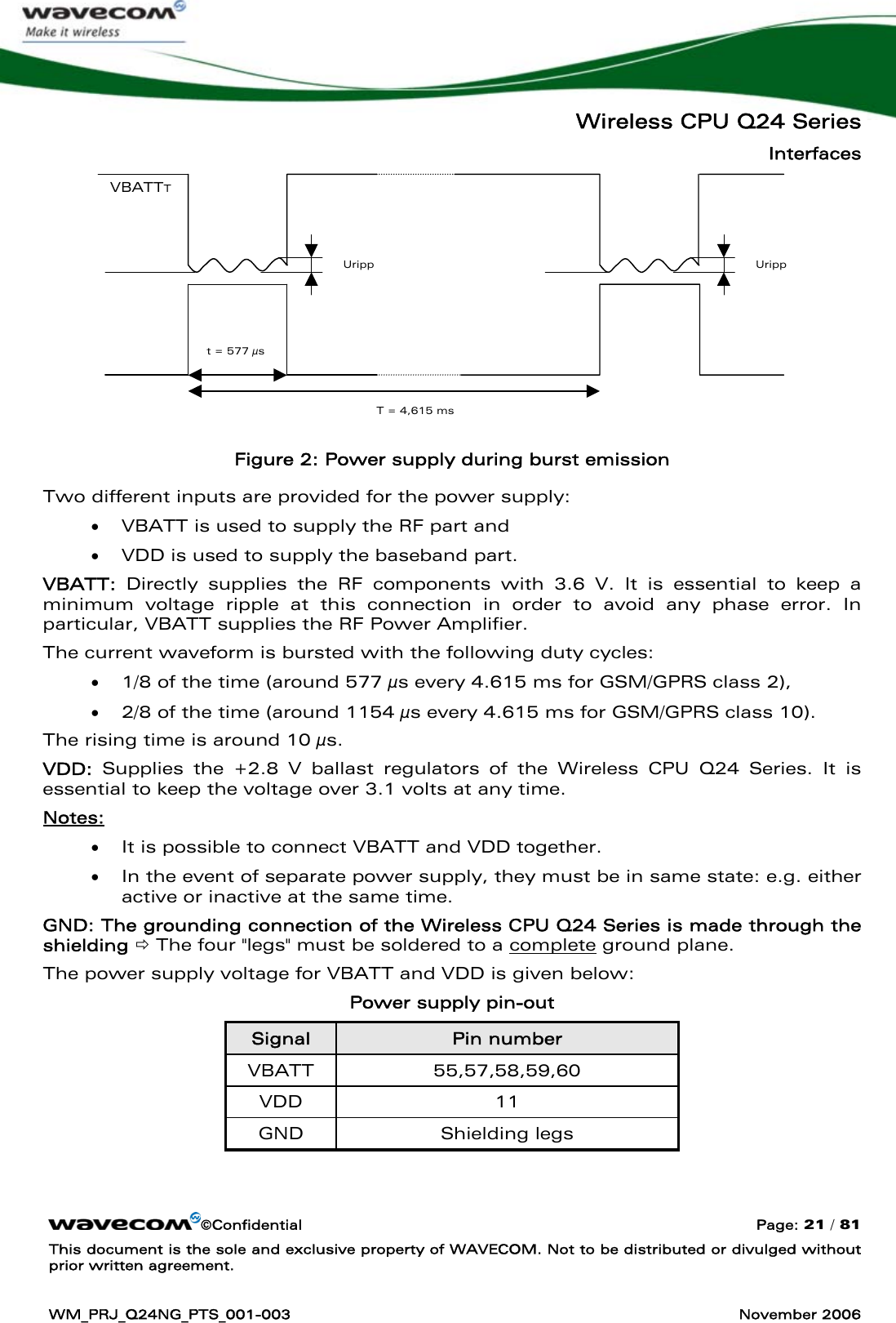
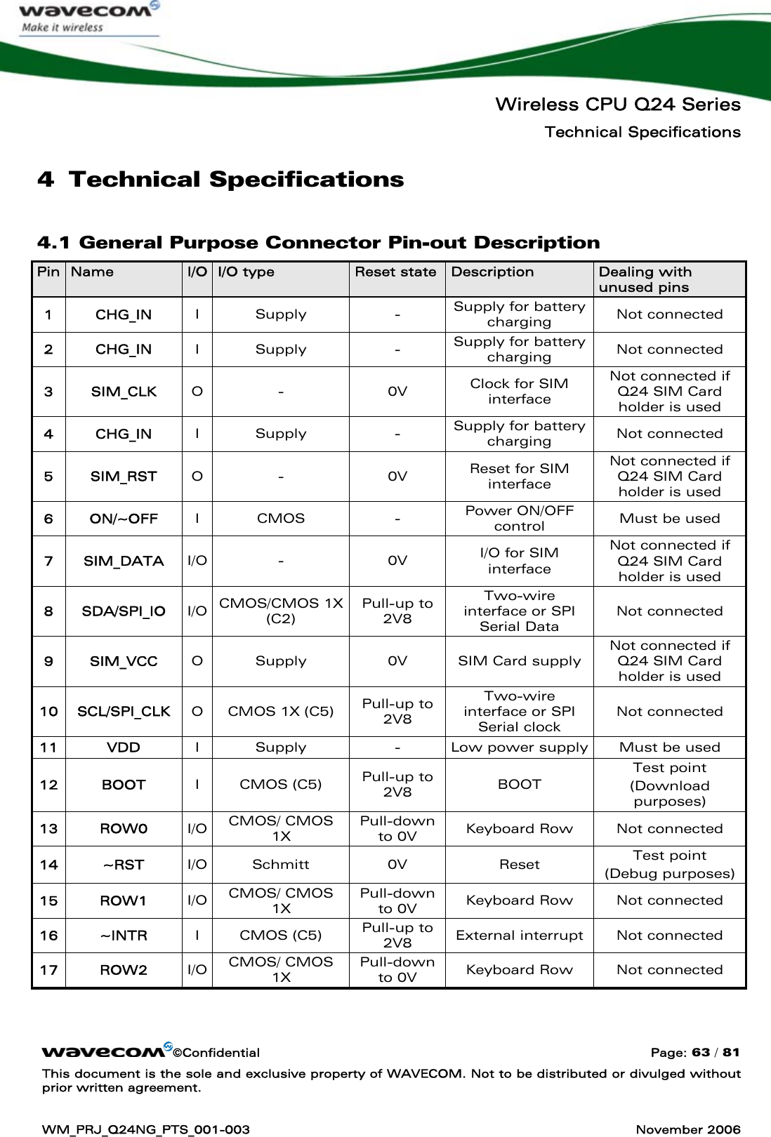
![Wireless CPU Q24 Series Interfaces ©Confidential Page: 23 / 81 This document is the sole and exclusive property of WAVECOM. Not to be distributed or divulged without prior written agreement. WM_PRJ_Q24NG_PTS_001-003 November 2006 Freq. (kHz) Uripp Max (mVpp) Freq. (kHz) Uripp Max (mVpp) Freq. (kHz) Uripp Max (mVpp) <100 50 800 4 1500 34 200 15.5 900 15.2 1600 33 300 6.8 1000 9.5 1700 37 400 3.9 1100 32 1800 40 500 4 1200 22 >1900 40 600 2 1300 29 700 8.2 1400 30 05101520253035404550200 400 600 800 1000 1200 1400 1600 1800Input Frequency (kHz)Uripp (mVpp)for f<100kHz Uripp Max = 50mVpp for f> 1800kHz Uripp Max = 40 mVpp Figure 3: Maximum voltage ripple (Uripp) versus Frequencies in GSM & DCS Refer to Wireless CPU Q24 Series Customer Design Guidelines [3], for further information on power supply design.](https://usermanual.wiki/Sierra-Wireless/Q24EX001/User-Guide-734426-Page-24.png)
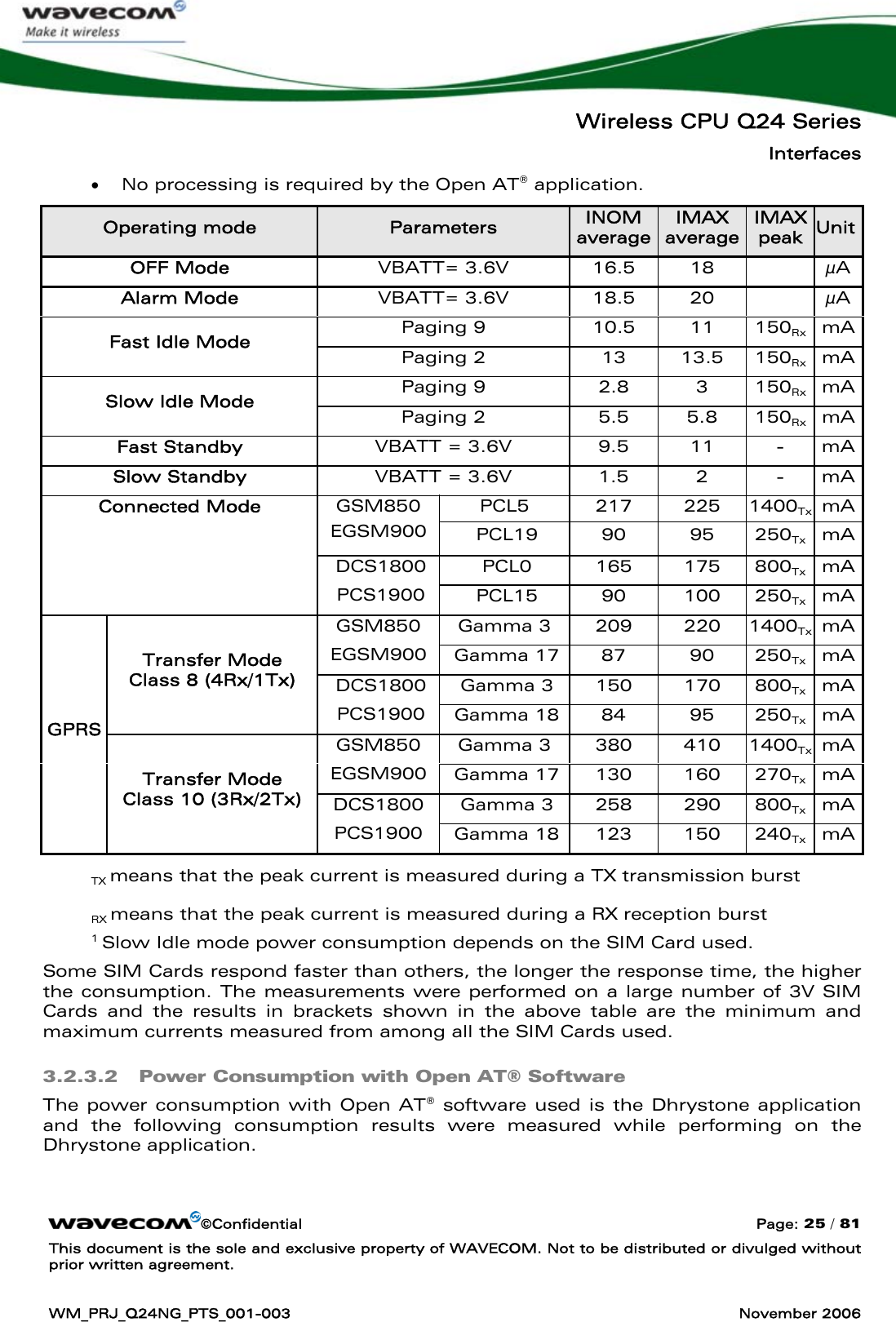
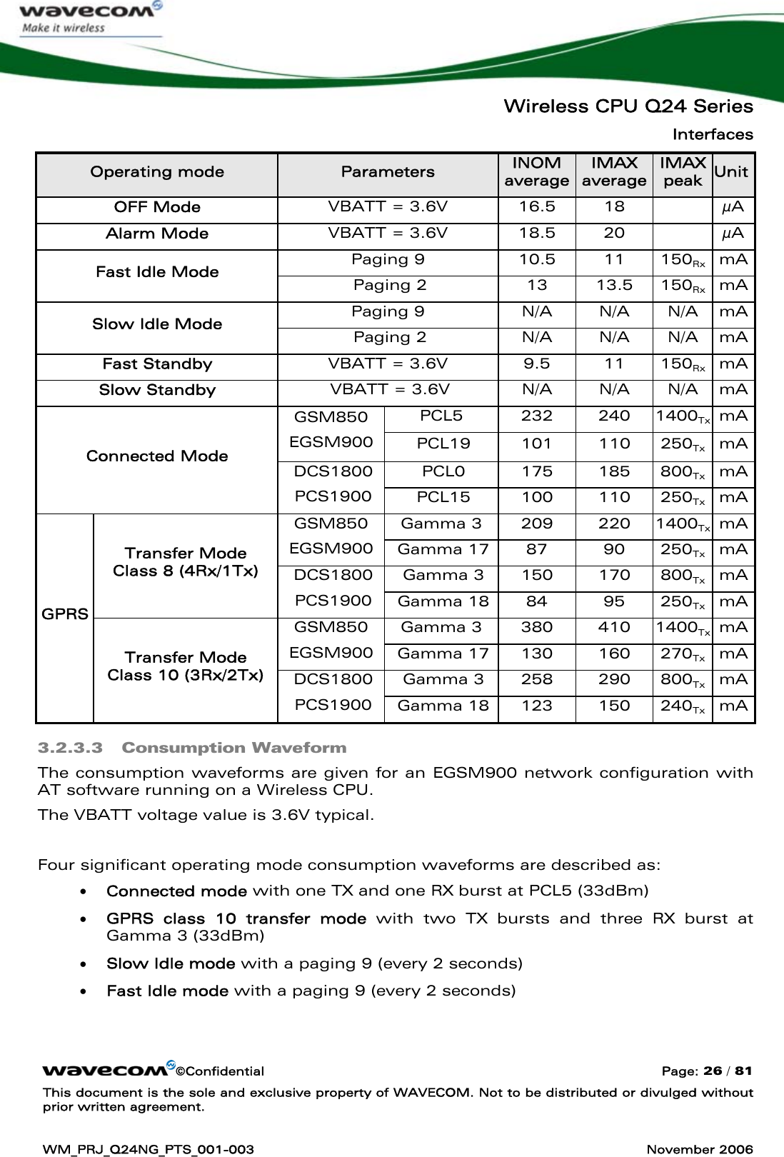
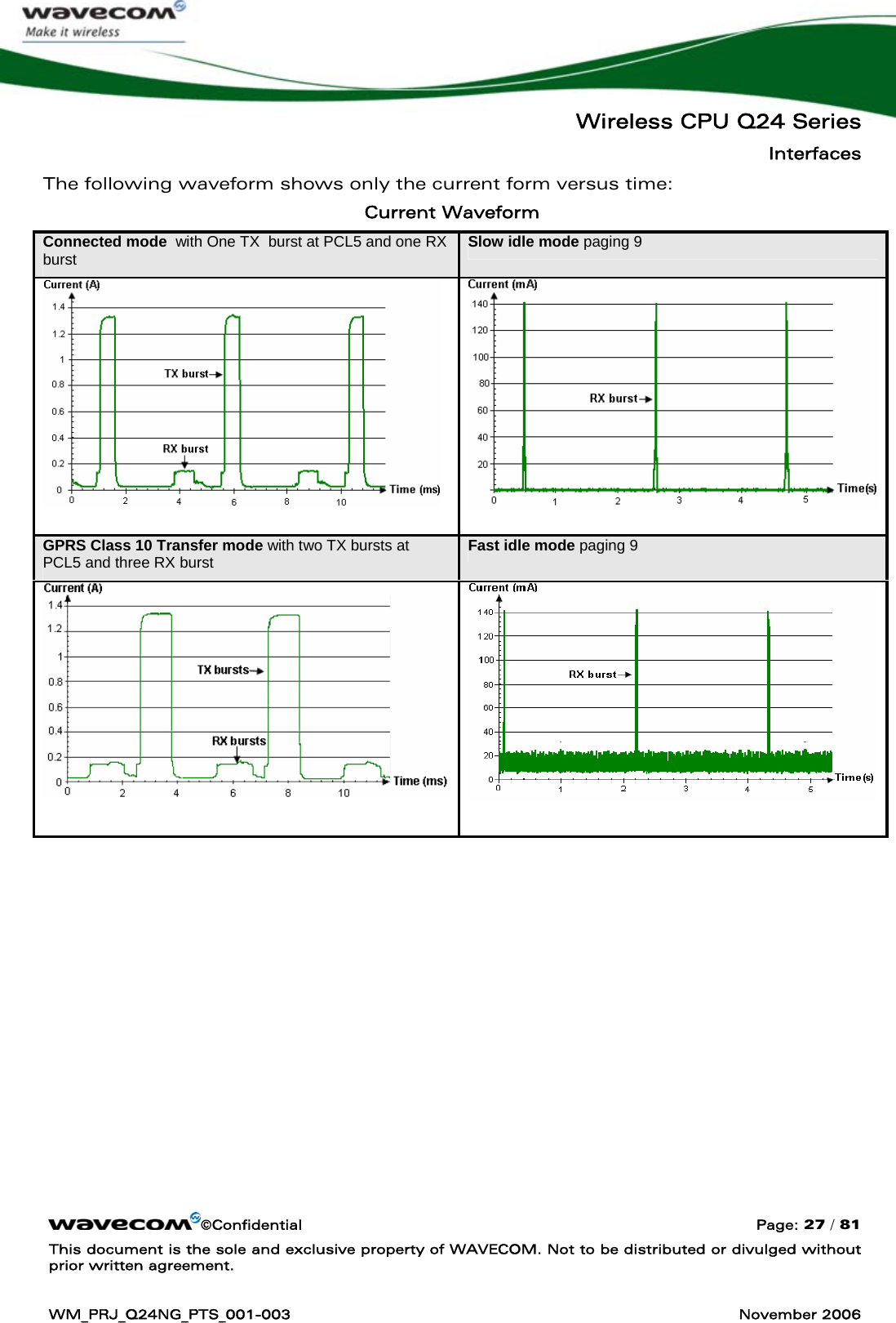
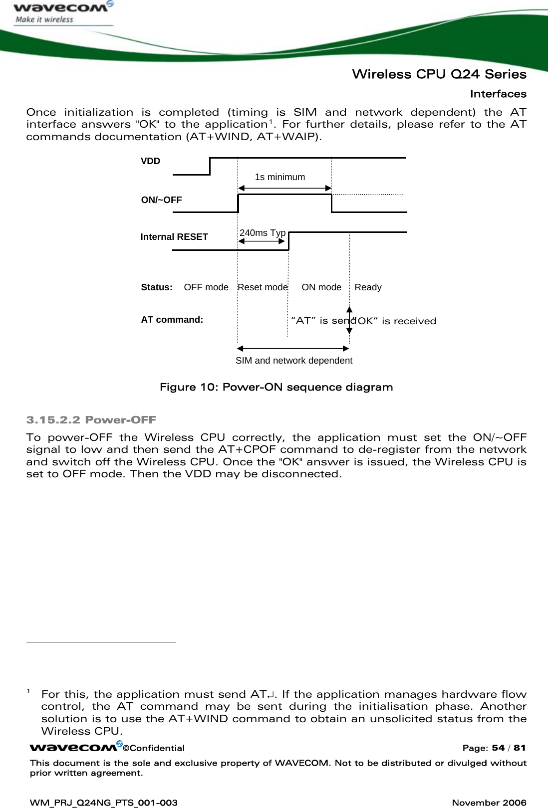
![Wireless CPU Q24 Series Interfaces ©Confidential Page: 24 / 81 This document is the sole and exclusive property of WAVECOM. Not to be distributed or divulged without prior written agreement. WM_PRJ_Q24NG_PTS_001-003 November 2006 3.2.3 Power Consumption The Wireless CPU Q24 Series support different power consumption modes: Working modes Comments OFF mode The Wireless CPU is in OFF mode. ALARM mode The Wireless CPU is in OFF mode with RTC block running, when an ALARM occurs, the Wireless CPU wakes-up automatically. FAST idle mode The Wireless CPU is synchronized with an RF GSM/GPRS network. The internal 26 MHz of the Wireless CPU is constantly active. SLOW idle mode The Wireless CPU is synchronized with an RF GSM/GPRS tester. The internal 26 MHz of the Wireless CPU is not constantly active. FAST Standby mode The SIM and Radio interface are deactivated via AT command or Open AT API: -The embedded application is running -The serial port remains active (AT commands are available). The internal 26 MHz of the Wireless CPU is constantly active. SLOW Standby mode This mode is similar to the FAST Standby mode. All the features are disabled (no GSM, no GPRS, no SIM and no Serial port). The internal 26 MHz of the Wireless CPU is not constantly active. Communication mode A GSM/GPRS communication is established with a RF GSM/GPRS network. The power consumption depends on the configuration used. It is for this reason that the following power consumption values are given for each modes, RF bands and software used (AT or Open AT®). All the following information is given, by assuming a 50 Ω RF output. Three VBATT values are used to measure the consumption, VBATTMIN (3.2V), VBATTMAX (4.5V) and VBATTTYP (3.6V). The average current is given for three VBATT values and peak current given is the maximum current peak measured with three VBATT voltages. For more information on power consumption measurement, hardware configuration, SIM used, and software Dhrystone application, see the AT Command Interface Guide or OS 6.57 [5] and Wireless CPU Q24 Series Customer Design Guidelines [3]. When Wireless CPU is in Alarm mode, no voltage must be applied to any pin of the 60-pin connector, except on the BAT-RTC (pin 56) for RTC operation or ON/~OFF (pin 6) to power-ON the Wireless CPU. 3.2.3.1 Power Consumption without Open AT® Processing The following measurement results are relevant only when: • There is no Open AT® application, • The Open AT® application is disabled,](https://usermanual.wiki/Sierra-Wireless/Q24EX001/User-Guide-734426-Page-25.png)
![Wireless CPU Q24 Series Interfaces ©Confidential Page: 29 / 81 This document is the sole and exclusive property of WAVECOM. Not to be distributed or divulged without prior written agreement. WM_PRJ_Q24NG_PTS_001-003 November 2006 Pin description Signal Pin I/O I/O type Reset state Description Multiplexed with SPI_CLK 10 O CMOS 1X (C5) Pull-up to 2V8 SPI Serial Clock SCL SPI_IO 8 I/O CMOS / CMOS 1X (C2) Pull-up to 2V8 SPI Data SDA SPI_AUX 26 O CMOS 1X (C3) 2V8 SPI Aux. Enable GPO0 (C2), (C3) and (C5): To obtain more details on I/O type, refer to chapter "I/O Circuit diagram" 3.4.3 Two-wire Bus Interface (I2C) The two-wire bus interface includes a CLK signal (SCL) and a DATA signal (SDA) complying with a standard two-wire bus interface. The frequency clock is programmable either to a 96 kHz or a 400 kHz. Pin description Signal Pin I/O I/O type Reset state Description SCL 10 O CMOS 1X (C5) Pull-up to 2V8 Serial Clock SDA 8 I/O CMOS / CMOS1X (C2) Pull-up to 2V8 Serial Data (C2) and (C5): To obtain more details on I/O type, refer to chapter "I/O Circuit diagram" 3.5 Keyboard Interface Equivalent circuit Key 2V8 GND 2V8 Key Press Detector Row0 Col0 D Q COLUMN 0 COLUMN 4 CLOCK GND COLUMN [0] Key Release Detector Q D ROW 0 ROW 4 ROWCK ROW [0] Select Select](https://usermanual.wiki/Sierra-Wireless/Q24EX001/User-Guide-734426-Page-30.png)
![Wireless CPU Q24 Series Interfaces ©Confidential Page: 32 / 81 This document is the sole and exclusive property of WAVECOM. Not to be distributed or divulged without prior written agreement. WM_PRJ_Q24NG_PTS_001-003 November 2006 3.7 Auxiliary Serial Link (UART2) For specific applications, an auxiliary serial interface (UART2) is available on the Wireless CPU Q24 Series. E.g. Bluetooth connectivity: See AT commands interface guide (Bluetooth) [5]. Figure 5: UART2 Serial Link signals Pin description Signal Pin I/O I/O type Reset state Description Multiplexed with CT103 / TXD2 18 I CMOS (C4) Pull down to 0V Transmit serial data GPI CT104 / RXD2 20 O CMOS 1X (C3) 2V8 Receive serial data GPO2 CT106 / CTS2 24 O CMOS 2X (C1) High impedance Clear To Send GPIO0 CT105 / RTS2 35 I CMOS High impedance Request To Send GPIO5 (C1), (C3) and (C4): To obtain more details on I/O type, refer to chapter "I/O Circuit diagram" 3.8 SIM Interface 3.8.1 General Description The following five signals are available: • SIM_VCC: SIM power supply. • SIM_RST: Reset. • SIM_CLK: Clock. • SIM_DATA: I/O port. • SIM_PRES: SIM Card detection. The SIM interface controls a 3V / 1V8 SIM (and a 5V SIM through an external SIM driver). This interface is fully compliant with the GSM 11.12 recommendations concerning SIM functions.](https://usermanual.wiki/Sierra-Wireless/Q24EX001/User-Guide-734426-Page-33.png)
![Wireless CPU Q24 Series Interfaces ©Confidential Page: 33 / 81 This document is the sole and exclusive property of WAVECOM. Not to be distributed or divulged without prior written agreement. WM_PRJ_Q24NG_PTS_001-003 November 2006 Pin description Signal Pin I/O I/O type Reset state Description SIM_CLK 3 O 2V9/1V8 0V SIM Clock SIM_RST 5 O 2V9/1V8 0V SIM Reset SIM_DATA 7 I/O 2V9/1V8 0V SIM Data SIM_VCC 9 O 2V9/1V8 0V SIM Power Supply SIM_PRES 50 I 2V8 High impedance SIM Card Detect Caution: Disturbances (digital noise, ESD) in the SIM signals may interrupt the Wireless CPU functionality, a good layout of these signals are recommended: • Ground separation between SIM signals and others signals • ESD protections (Refer to Wireless CPU Q24 Series Customer Design Guidelines [3]) Electrical Characteristics Parameters Conditions Min Type Max Unit SIM_DATA VIH IIH = ± 20 μA 0.7xSIMVCC V SIM_DATA VIL IIL = 1 mA 0.3xSIMVCC V SIM_RST, SIM_CLK VOH Source current = 20 μA 0.9xSIMVCC V SIM_DATA Source current = 20 μA 0.8xSIMVCC V SIM_RST, SIM_DATA, SIM_CLK VOL Sink current = -200 μA 0.4 V SIMVCC = 2.9V 2.84 2.90 2.96 V SIM_VCC Output Voltage SIMVCC = 1.8V 1.77 1.8 1.86 V SIM_CLK Rise/Fall Time Loaded with 30 pF 20 ns SIM_RST, Rise/Fall Time Loaded with 30 pF 20 ns SIM_DATA, Rise/Fall Time Loaded with 30 pF 0.7 μs SIM_CLK Frequency 3.25 MHz Note for SIM_PRES connection: • When not used, SIM_PRES must be tied to 2V8 • When used, a low to high transition means that the SIM Card is inserted and a high to low transition means that the SIM Card is removed.](https://usermanual.wiki/Sierra-Wireless/Q24EX001/User-Guide-734426-Page-34.png)
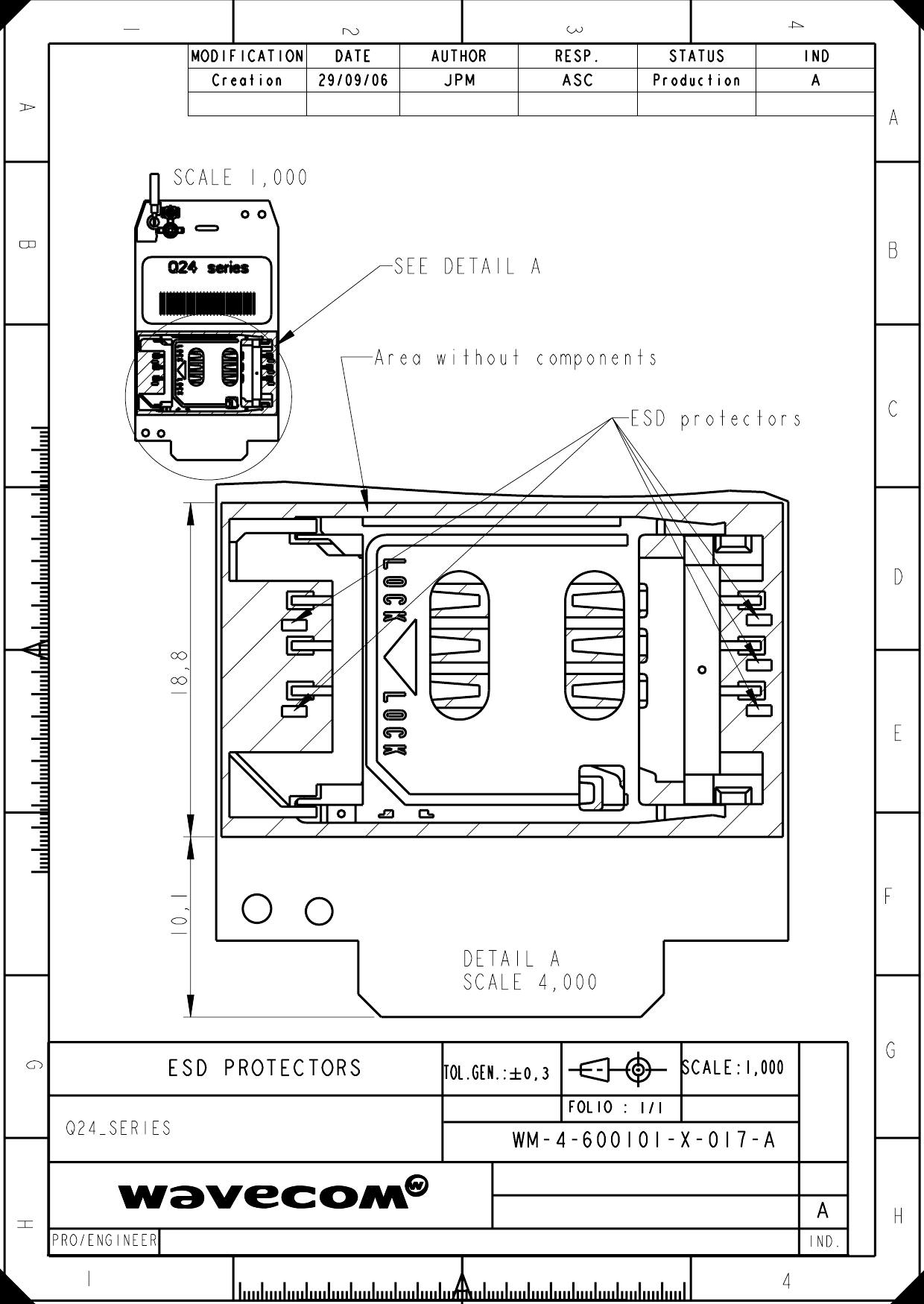
![Wireless CPU Q24 Series Interfaces ©Confidential Page: 34 / 81 This document is the sole and exclusive property of WAVECOM. Not to be distributed or divulged without prior written agreement. WM_PRJ_Q24NG_PTS_001-003 November 2006 3.8.2 SIM Card Holder An optional SIM Card holder may be placed on top of Wireless CPU. This SIM Card holder does not use the SIM_PRES signal. Caution: Customers are advised to verify that the SIM Card environmental specification used is compliant with the Wireless CPU Q24NG environmental specifications [3] (see the Wireless CPU Q24NG Product Technical Specification WM_PRJ_Q24NG_PTS_001). Any application must be qualified by the customer with the SIM Card in storage, transportation and operation. Some ESD protections were placed to protect SIM form ESD stress; ESD protection position is described in Figure 6 and should be taken into account during a mechanical design. Figure 6: SIM Card holder constraints (see next page)](https://usermanual.wiki/Sierra-Wireless/Q24EX001/User-Guide-734426-Page-35.png)
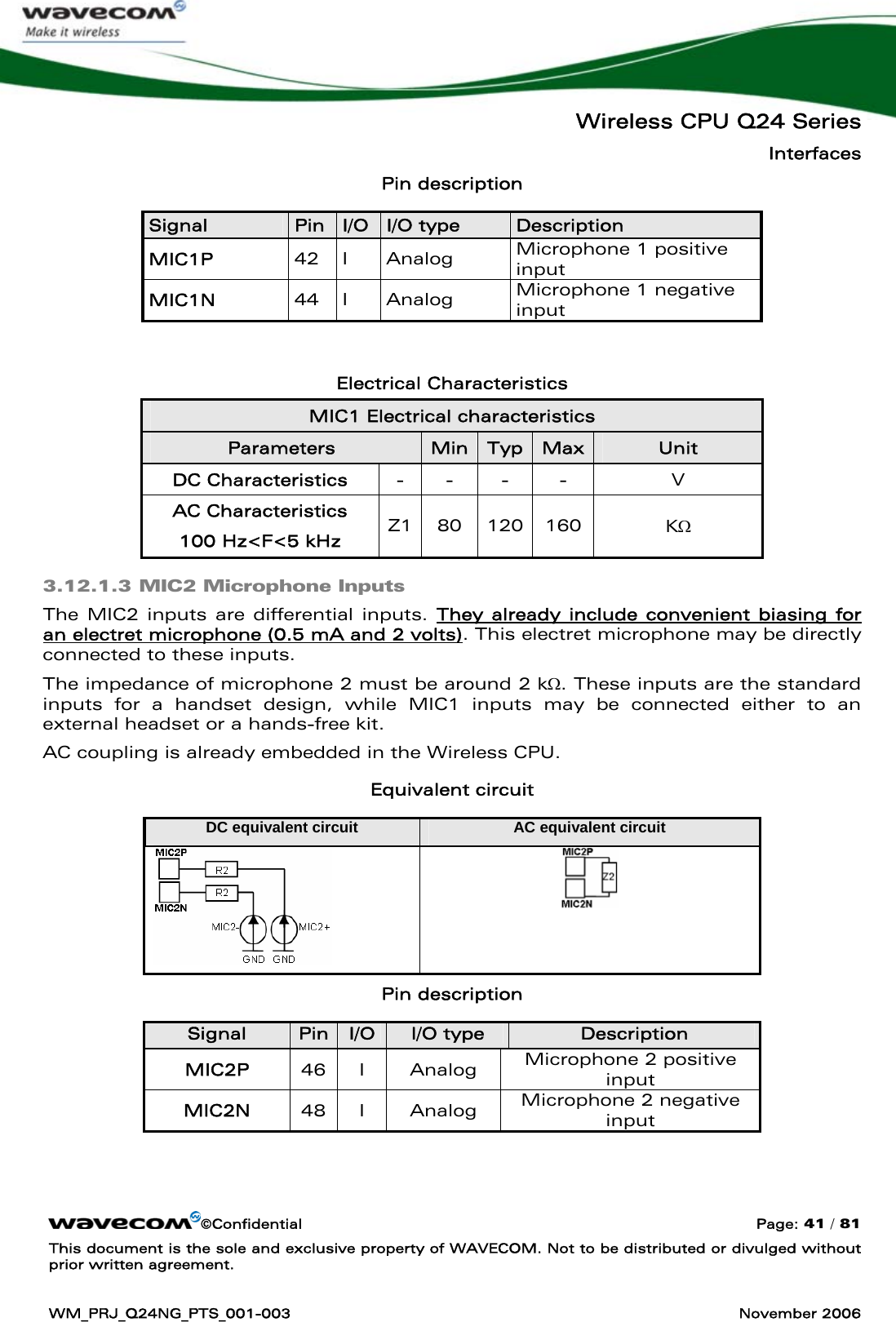
![Wireless CPU Q24 Series Interfaces ©Confidential Page: 39 / 81 This document is the sole and exclusive property of WAVECOM. Not to be distributed or divulged without prior written agreement. WM_PRJ_Q24NG_PTS_001-003 November 2006 Caution: When speakers and microphones are exposed to the external environment, it is recommended to add ESD protection on the audio interface lines. 3.12.1 Microphone Inputs The MIC2 inputs already include the biasing for an electret microphone, thus allowing easy connection to a handset. The MIC1 inputs do not include an internal bias. MIC1/SPK1 may be used for a hands-free system or a handset, including biasing circuit for the microphone. The microphone connections may be either differential or single-ended, but using a differential connection in order to reject common mode noise and TDMA noise is strongly recommended. Caution: While using a single-ended connection, ensure to have a good ground plane, a good filtering as well as shielding, in order to avoid any disturbance on the audio path. 3.12.1.1 Common Microphone Input Characteristics Both microphone inputs are designed with the following audio transmit characteristics: Internal audio filter characteristics Frequency Gain 0-150 Hz < -22 dB 150-180 Hz < -11 dB 180-200 Hz < -3 dB 200-3700 Hz 0 dB >4000 Hz < -60 dB The gain in the MIC inputs are internally adjusted and may be tuned from -6.5 dB to 51.3 dB by using AT commands (refer to AT commands documentation [5]).](https://usermanual.wiki/Sierra-Wireless/Q24EX001/User-Guide-734426-Page-40.png)
![Wireless CPU Q24 Series Interfaces ©Confidential Page: 40 / 81 This document is the sole and exclusive property of WAVECOM. Not to be distributed or divulged without prior written agreement. WM_PRJ_Q24NG_PTS_001-003 November 2006 Microphone gain versus Max input voltage Using Controller 1 Using Controller 2 Transmit Gain (dB) Max Vin (mVrms) Transmit Gain (dB) Max Vin (mVrms) +30 43.80 -6.5 3031 +33 31.01 -6 2861 +36 21.95 0 1434 +39 15.54 +9.5 480 +42 11 +10 454 +45 7.79 +30.3 43.80 +48 5.51 +30.8 41.36 +51 3.9 +50.8 4.14 - - +51.3 3.90 * For more details, refer to the AT commands documentation [5] 3.12.1.2 MIC1 Microphone Inputs The MIC1 inputs are differential and do not include internal bias. To use these inputs with an electret microphone, bias must be generated outside the Wireless CPU Q24 Series in accordance with the characteristic of this electret microphone. These inputs are the standard inputs used either for an external headset or a hands-free kit. The impedance of microphone 1 must be around 2 kΩ. AC coupling is already embedded in the Wireless CPU. Equivalent circuits DC equivalent circuit AC equivalent circuit](https://usermanual.wiki/Sierra-Wireless/Q24EX001/User-Guide-734426-Page-41.png)
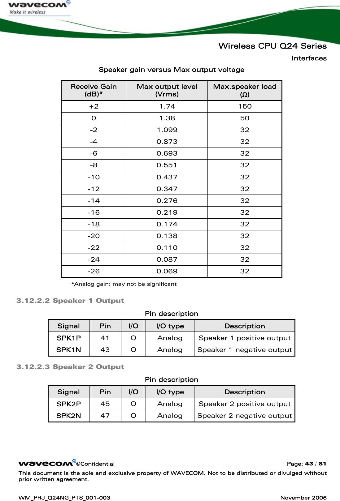
![Wireless CPU Q24 Series Interfaces ©Confidential Page: 42 / 81 This document is the sole and exclusive property of WAVECOM. Not to be distributed or divulged without prior written agreement. WM_PRJ_Q24NG_PTS_001-003 November 2006 Electrical Characteristics MIC2 Electrical characteristics Parameters Min Typ Max Unit MIC2- 0.225 0.35 0.475 V MIC2+ 2.025 2.15 2.275 V Output current 0.5 1 mA Internal biasing DC Characteristics R2 900 1150 1400 Ω AC Characteristics 100 Hz<F<5 kHz Z2 1.2 1.5 1.8 KΩ 3.12.2 Speaker Outputs Two speaker outputs are available: SPK1 and SPK2. Both speaker outputs may be represented as follows: Equivalent circuit 3.12.2.1 Common Speaker Output Characteristics The connection may be differential or single-ended, but using a differential connection to reject common mode noise and TDMA noise is strongly recommended. Moreover, in single-ended mode, the power is reduced by two, compare to the differential mode Caution: When using a single-ended connection, ensure to have a good ground plane, a good filtering as well as a good shielding in order to avoid any disturbance on the audio path. Speaker outputs SPK1 and SPK2 are push-pull amplifiers and may be loaded down to 150Ω and up to 1 nF The impedance of the speaker amplifier outputs in differential mode is: R ≤ 1 Ω +/-10 % . When speaker output is not used, the speaker interface is in three states and a 20K +/-30% impedance is kept between SPK1N and SPK1P as well as SPK2N and SPK2P. These outputs are differential and the output power may be adjusted by step of 2 dB. The output may be directly connected to a speaker. The gain in the speaker outputs are internally adjusted and may be tuned by using AT commands (refer to the AT commands documentation [5]). Q24 Series](https://usermanual.wiki/Sierra-Wireless/Q24EX001/User-Guide-734426-Page-43.png)
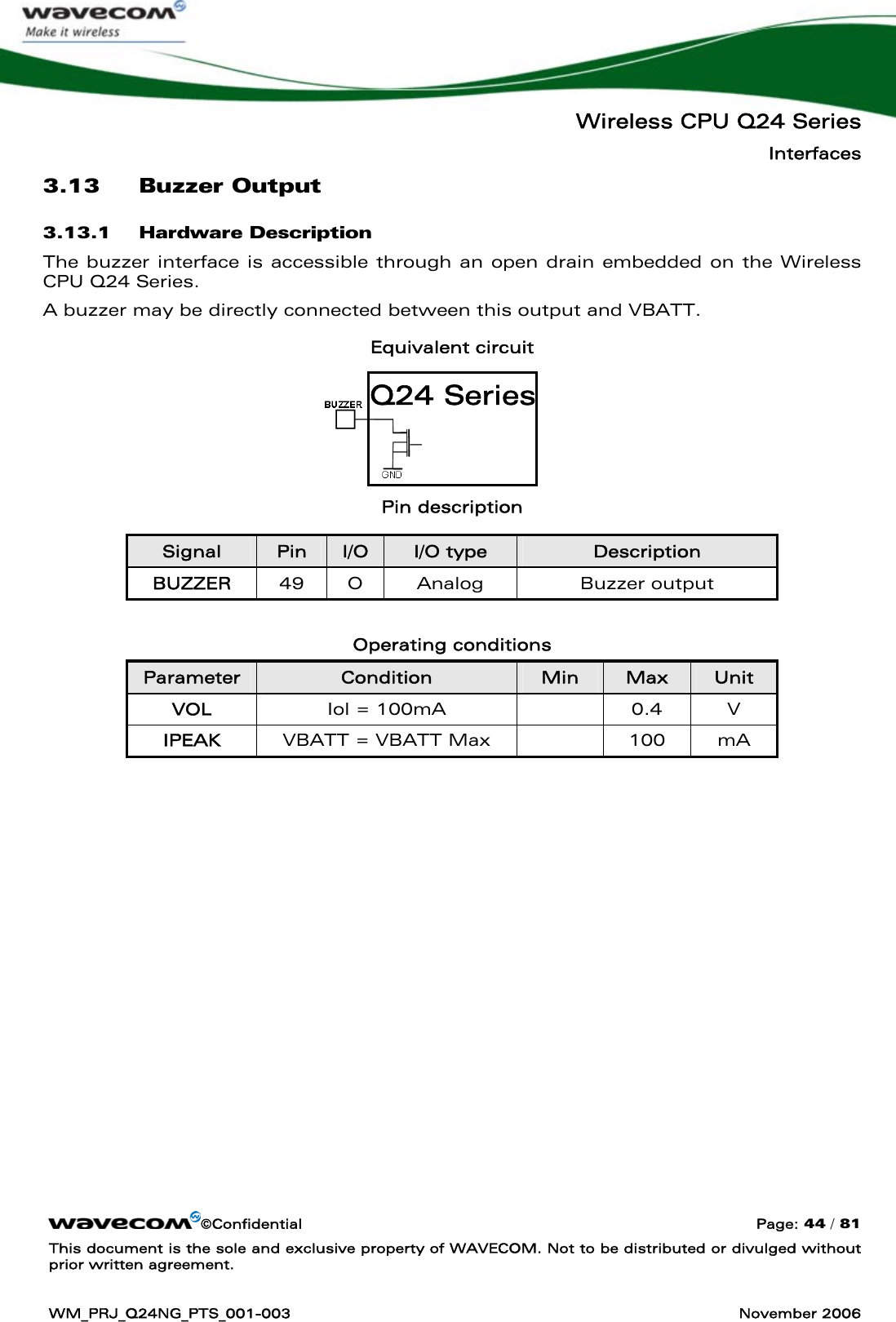
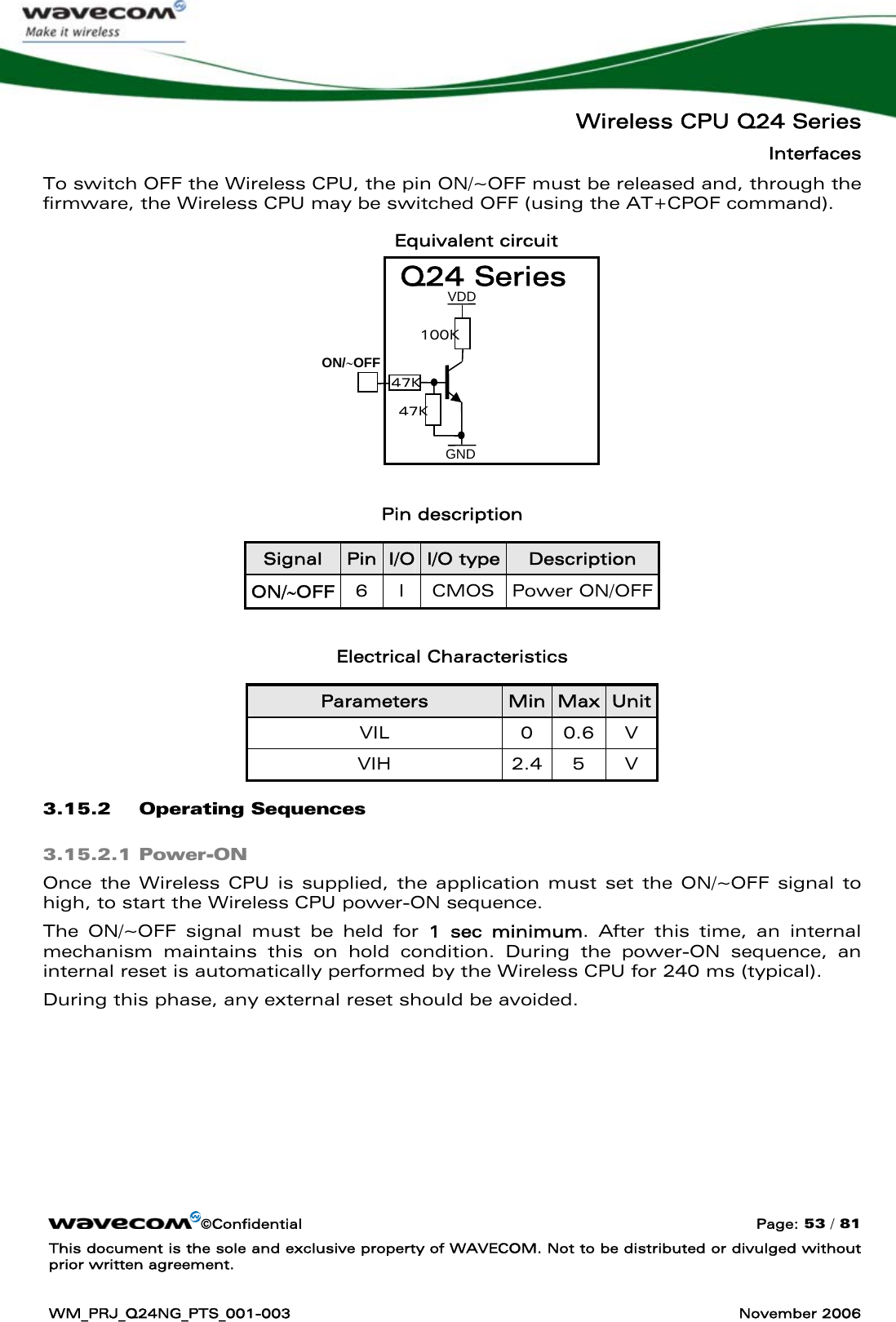
![Wireless CPU Q24 Series Interfaces ©Confidential Page: 45 / 81 This document is the sole and exclusive property of WAVECOM. Not to be distributed or divulged without prior written agreement. WM_PRJ_Q24NG_PTS_001-003 November 2006 Caution: A diode against transient peak voltage must be connected as described below. Figure 7: Buzzer connection For the implementation of the buzzer interface, refer to the Customer Design Guidelines [3]. 3.14 Battery Charging Interface 3.14.1 Hardware Description Caution: The battery charging interface does not allow the Wireless CPU to be supplied and is only used to charge a battery connected to VBATT. Battery charging is performed through a switching transistor connecting the VBATT signal to the Charger (CHG_IN signal). The switching transistor is controlled by the operating system with two kinds of algorithms. Equivalent circuit BAT_TEMP Q24 Series CHG_IN Charger controller 5K6 T Charger detection VBATT](https://usermanual.wiki/Sierra-Wireless/Q24EX001/User-Guide-734426-Page-46.png)
![Wireless CPU Q24 Series Interfaces ©Confidential Page: 47 / 81 This document is the sole and exclusive property of WAVECOM. Not to be distributed or divulged without prior written agreement. WM_PRJ_Q24NG_PTS_001-003 November 2006 Pin description Signal Pin number I/O I/O type Description CHG_IN 1, 2, 4 I Analog Current source input BAT_TEMP 38 I Analog A/D converter Electrical Characteristics Parameter Min Typ Max Unit Resolution 10 bits Sampling rate 90.3 Ksps/s Input Impedance (R) 1M kΩ Input Impedance (C) 100 nF BAT_TEMP Input signal range 0 2V8 V CHG_IN <BattLevelMax+0.5* - 6 V * The min CHG_IN voltage depends on the battery characteristics. (see the following chapter). 3.14.2 Temperature Monitoring Temperature monitoring is available only for the Li-Ion battery with algorithm 1. The BAT-TEMP ADC input must be used to sample the temperature analog signal provided by an NTC temperature sensor. The minimum and maximum temperature range may be set by an AT command (See the Li-Ion charging algorithm). 3.14.3 Ni-Cd / Ni-Mh Charging Algorithm During the charging process of a Ni-Cd and Ni-Mh battery, it is required to tune software parameters in the Wireless CPU operating system: AT+WBCM=<Mode>, <ChargeInd>, <BattLevelMax>, <BattLevelMin>, <TPulseInCharge>, <TPulseOutCharge>, <BattIntRes>, <BattChangeLevel > (See the AT command Interface Guide [5]). Caution: The parameters need to be tuned according to the battery specifications.](https://usermanual.wiki/Sierra-Wireless/Q24EX001/User-Guide-734426-Page-48.png)
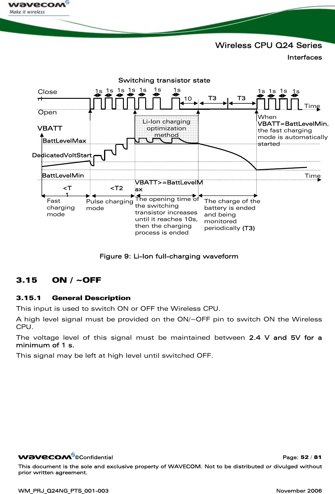
![Wireless CPU Q24 Series Interfaces ©Confidential Page: 49 / 81 This document is the sole and exclusive property of WAVECOM. Not to be distributed or divulged without prior written agreement. WM_PRJ_Q24NG_PTS_001-003 November 2006 Note: A charger is connected to the CHG_IN pin of the Wireless CPU. Figure 8: Ni-Cd / Ni-Mh charging waveform 3.14.4 Li-Ion Charging Algorithm During the charging process of a Li-Ion battery, it is required to tune parameters embedded in the Wireless CPU operating system: AT+WBCM=<Mode>,<ChargeInd>,<TdeltaTemp>,<BattLevelMax>, <BattLevelMin>, <MaxVoltPulse>, <MaxBatteryTemp>,<MinBatteryTemp>,<Charging_Current>, <DedicatedVoltStart>, <Battery_Pulse_Charging_Timeout>, <Battery_Fast_Charging_Timeout>, <TPulseOutCharge>, <BattIntRes>, <BattChangeLevel> (See the AT command Interface Guide [5]). Caution: The parameters need to be tuned according to the battery specifications. The main parameters to be tuned are: Parameters related to time: • BatteryFastChargingTimeout: Maximum duration of the fast charging period. (T1) • BatteryPulseChargingTimeout: Maximum duration of the charging pulse period.(T2) • TPulseOutCharge: Monitoring time of the VBATT voltage when charging process is not activated(T3) Parameters related to voltage: • BattLevelMin: Minimum VBATT voltage allowed by the battery (>3.2V) • BattLevelMax: Maximum VBATT voltage allowed by the battery (<4.5V) • DedicatedVoltStart: Pulse charging is started above this threshold voltage Parameter related to charging current: • ChargingCurrent: Charging current delivered by the charger VBATT=BattLevelMax:Charging process ended VBATT=BattLevelMin:Charging process automatically started T3 T3 T2 T2 T1 T1 T1 T2 Switching transistor: Closed Open Time VBATT BattLevelMax BattLevelMin Time](https://usermanual.wiki/Sierra-Wireless/Q24EX001/User-Guide-734426-Page-50.png)
![Wireless CPU Q24 Series Interfaces ©Confidential Page: 55 / 81 This document is the sole and exclusive property of WAVECOM. Not to be distributed or divulged without prior written agreement. WM_PRJ_Q24NG_PTS_001-003 November 2006 Figure 11: Power-OFF sequence diagram Caution: It is not allowed to power-OFF the Wireless CPU by disconnecting the supply pins VBATT and VDD. Note: Instead of sending AT+CPOF, use the Wireless CPU external interrupt pin (see the External interrupt) 3.16 BOOT (optional) This input may be used to download software to the Flash memory of the Wireless CPU. For applications based on AT commands, this is a backup download procedure (refer to document [3] Customer Design Guidelines). The internal BOOT procedure starts when this pin is low during Wireless CPU reset. Caution: • This BOOT pin must be left open for normal use or Xmodem download. • The nominal firmware download procedure uses the Xmodem. In Internal BOOT mode, low level must be set through a 1KΩ resistor. • BOOT = logical state 0, for download mode and • BOOT = logical state 1, for normal mode. VDD ON/~OFF Status: Ready OFF mode Network dependent AT+CPOF “OK” answer](https://usermanual.wiki/Sierra-Wireless/Q24EX001/User-Guide-734426-Page-56.png)
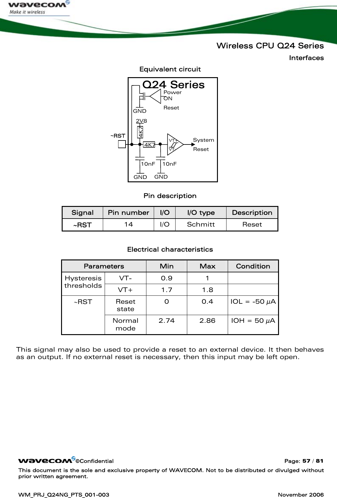
![Wireless CPU Q24 Series Interfaces ©Confidential Page: 58 / 81 This document is the sole and exclusive property of WAVECOM. Not to be distributed or divulged without prior written agreement. WM_PRJ_Q24NG_PTS_001-003 November 2006 If used (as an emergency reset), it must be driven either by an open collector or an open drain output: Figure 12: RST pin connection For the implementation of the reset interface, refer to the Customer Design Guidelines 3.17.2 Reset Sequence To activate the "emergency "reset sequence, the ~RST signal must be set to low for 500 μs minimum. As soon as the reset is completed, the AT interface answers "OK" to the application. In this case, the application must send AT↵. If the application manages hardware flow control, the AT command may be sent during the initialization phase. Another solution is to use the AT+WIND command to obtain an unsolicited status from the Wireless CPU. For further details, refer to the AT commands documentation [5]. Figure 13: Reset sequence diagram 3.18 External Interrupt (~INTR) The Wireless CPU Q24 Series provide an external interrupt input ~INTR. This input is highly sensitive. An interrupt is activated on a falling edge. If this signal is not used, it may be left open. If used, this input must be driven either by an open collector or an open drain output. GND ~RST External reset External reset Status: Ready ON mode Min 500µsTyp: 2ms Ready Reset mode SIM and network dependent](https://usermanual.wiki/Sierra-Wireless/Q24EX001/User-Guide-734426-Page-59.png)
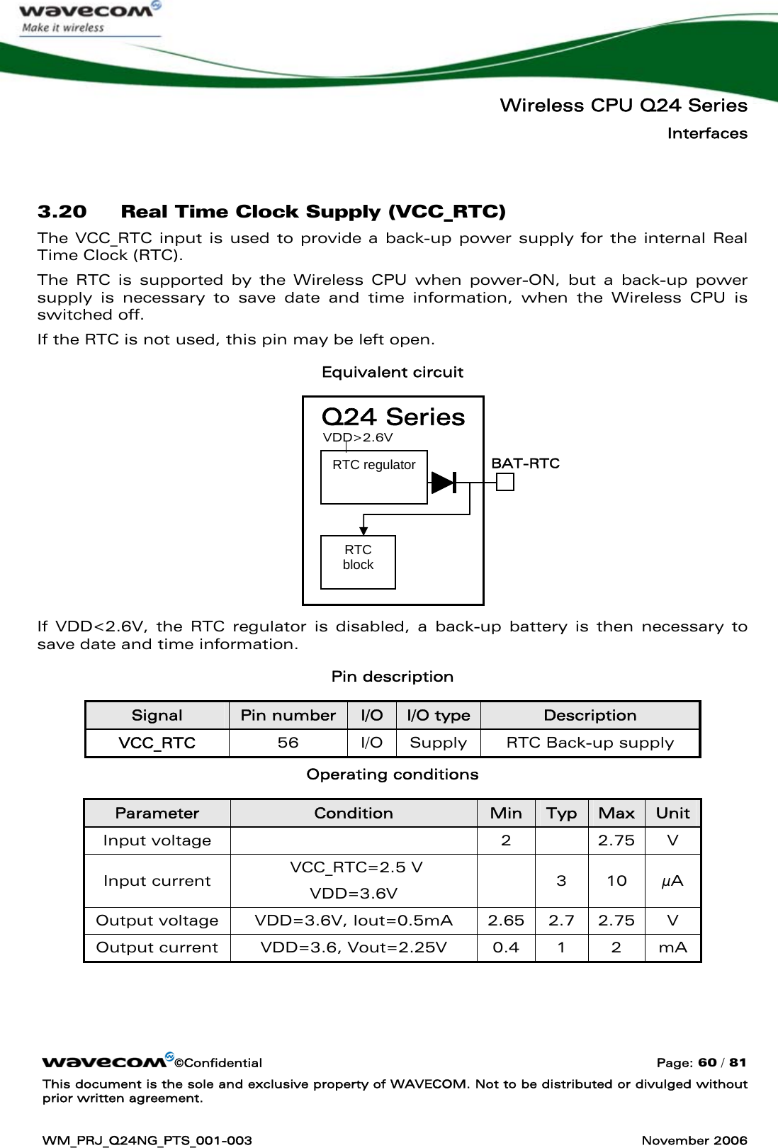
![Wireless CPU Q24 Series Environmental Specifications ©Confidential Page: 69 / 81 This document is the sole and exclusive property of WAVECOM. Not to be distributed or divulged without prior written agreement. WM_PRJ_Q24NG_PTS_001-003 November 2006 5.1 Environmental Qualifications For the Wireless CPU Q24 Classic, Q24 Plus, and Q24 Extended, applied environmental qualifications are defined in the table below: ENVIRONMENTAL CLASSESTYPE OF TEST STANDARDS STORAGE TRANSPORTATION OPERATING (PORT USE)Class 1.2 Class 2.3 Class 7.3Cold IEC 68-2.1 -25° C 72 h -40° C 72 h -20° C (GSM900) 16 hAb test -10° C (GSM1800/1900) 16hDry heat IEC 68-2.2 +70° C 72 h +70° C 72 h +55° C 16 hBb testChange of temperature IEC 68-2.14 -40° / +30° C 5 cycles -20° / +30° C (GSM900) 3 cyclesNa/Nb test t1 = 3 h -10° / +30° C (GSM1800/1900):3 cycles t1 = 3 hDamp heat IEC 68-2.30 +30° C 2 cycles +40° C 2 cycles +40° C 2 cyclescyclic Db test 90% - 100% RH 90% - 100% RH 90% - 100% RHvariant 1 variant 1 variant 1Damp heat IEC 68-2.56 +30° C 4 days +40° C 4 days +40° C 4 daysCb testSinusoidal vibration IEC 68-2.6 5 - 62 Hz : 5 mm / sFc test 62 - 200Hz : 2 m / s23 x 5 sweep cycles5 - 20 Hz : 0.96 m2 / s3 10 -12 Hz : 0.96 m2 / s3Random vibration IEC 68-3.36 20 - 500Hz : - 3 dB / oct 12 - 150Hz : - 3 dB / octwide band Fdb test 3 x 10 min 3 x 30 min Figure 16: Q24 Classic, Q24 Plus and Q24 Extended Environmental classes For more details, refer to the document: "Environmental Control Plan" for Wireless CPU Q24 Series [2] Electro-Static Discharge (ESD): According to the EN 61000-4-2 standard, the maximum ESD level supported by the Wireless CPU series on contact discharges is ±1 kV on the 60-pin connector, ±2 kV on the antenna connector, and ±4 kV on the SIM Card holder.](https://usermanual.wiki/Sierra-Wireless/Q24EX001/User-Guide-734426-Page-70.png)
![Wireless CPU Q24 Series Environmental Specifications ©Confidential Page: 70 / 81 This document is the sole and exclusive property of WAVECOM. Not to be distributed or divulged without prior written agreement. WM_PRJ_Q24NG_PTS_001-003 November 2006 For the Wireless CPU Q24 Automotive, environmental qualification applied is defined in table below: Test Designation Standards Definition / Severities Resistance to Heat IEC 60068-2-2 Temperature: +85°C Duration: 504 h Resistance to cold test IEC 60068-2-30 Db Storage temperature: -40±2°C Storage time: 72 h Cooking Test - Temperature: +70 ±2°C Duration: 100 days Damp heat test IEC 60068-2-3 Storage temperature: +40±2°C Storage humidity: 95±3% Storage time: 21 days Damp heat cycle test IEC 60068-2-30 Db Upper temperature: +55±2°C Number of cycles: 10 Temperature change IEC 60068-2-14 Nb Low temperature: -40°±2°C High temperature: +85±2°C Total duration: 11 days Thermal Shock IEC 60068-2-14 Low temperature: -40°±2°C High temperature: +85±2°C Total duration: 200 hours Resistance to sinusoidal vibration IEC 60068-2-6 Fc [10 Hz to 16 Hz]: ±5 mm (peak) [16 Hz to 62 Hz]: 5 g (peak) [62 Hz to 200Hz]: 3g (peak) [200 Hz to 1000 Hz] 1g (peak) Test duration: 20 cycles Sweep directions: X / Y / Z Resistance to random vibration IEC 60068-2-64 Frequency range: 10 Hz - 2000 Hz Spectrum level: 0.1 g2/Hz at 10 Hz 0.01 g2/Hz at 250 Hz 0.0005 g2/Hz at 1000 Hz 0.0005 g2/Hz at 2000 Hz Duration: 16 h Vibration axis: X / Y / Z Resistance to mechanical shock IEC 68-2-27 Peak acceleration: 30g / 100g / 200g Direction: ±X, ±Y, ±Z ESD Test IEC 1000-4-2 1 kV contact discharge on 60-pin connector 2 kV contact discharge on RF connector 4kV contact discharge on SIM interface Figure 17: Q24 Automotive environmental classes For more details, refer to the document: "Automotive Environmental Control Plan" for Wireless CPU Q24 Series [1] 5.1.1 Reflow Soldering: The Wireless CPU Q24 Series do not support any reflow soldering.](https://usermanual.wiki/Sierra-Wireless/Q24EX001/User-Guide-734426-Page-71.png)