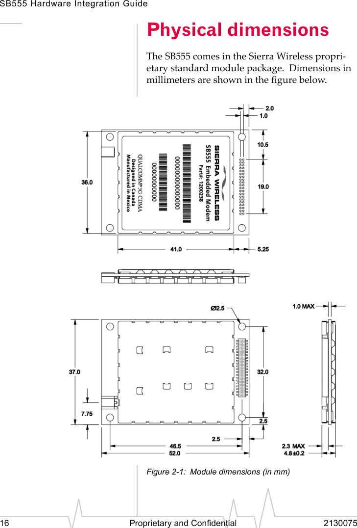
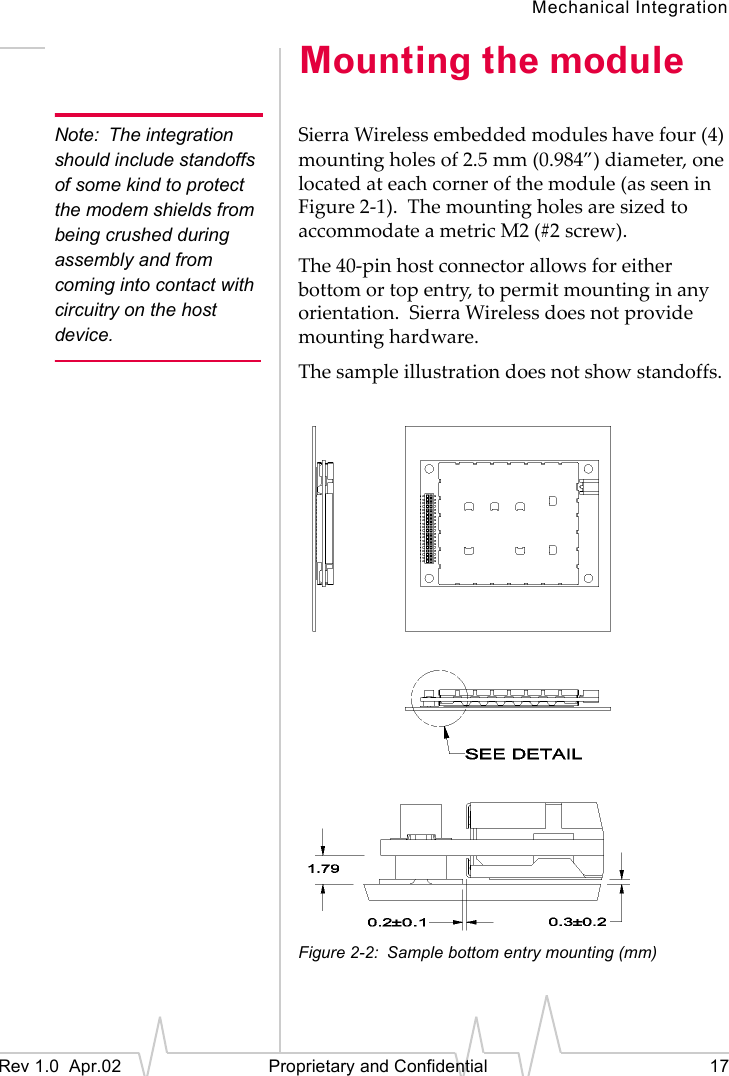
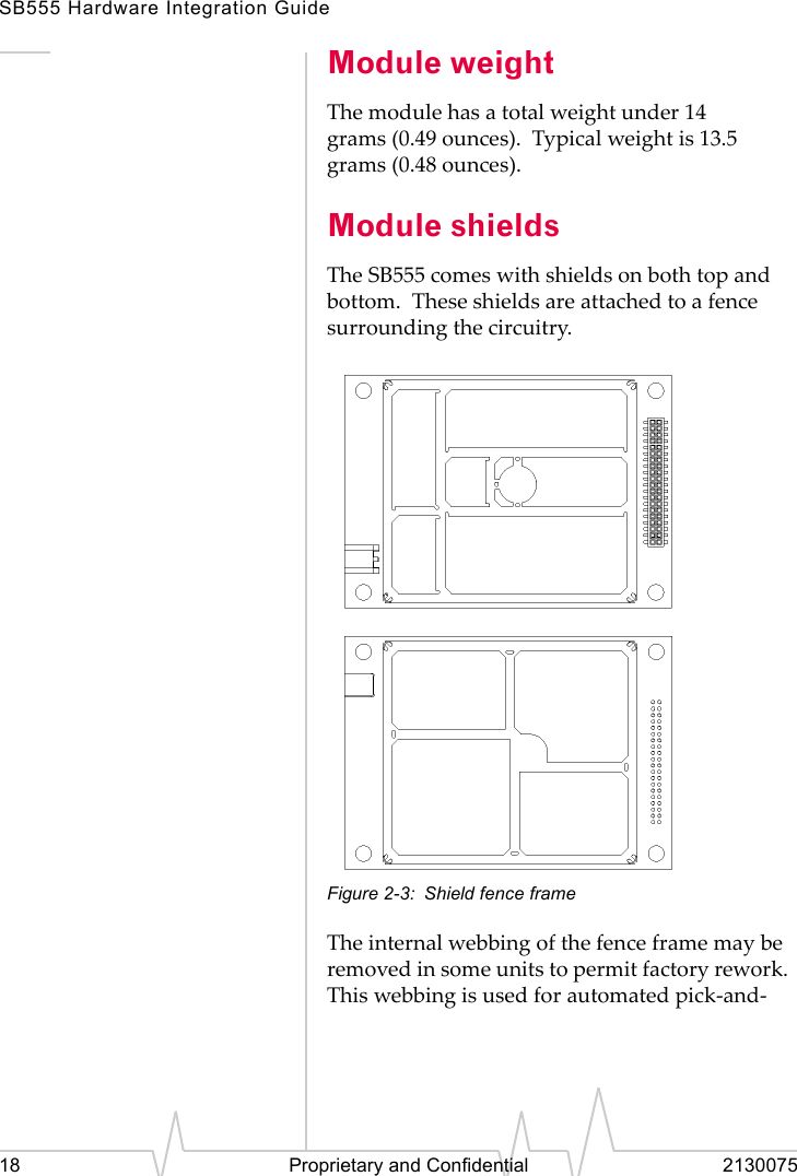
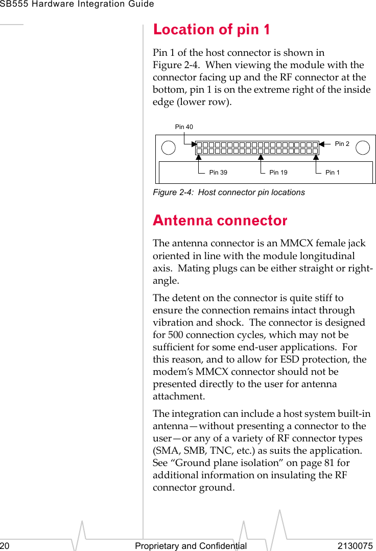
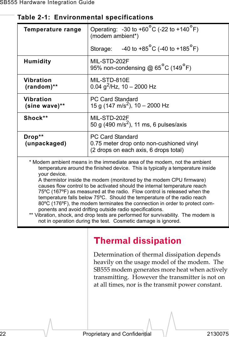
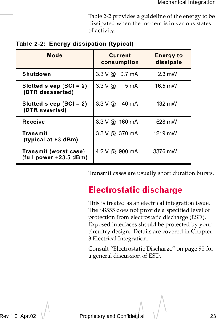
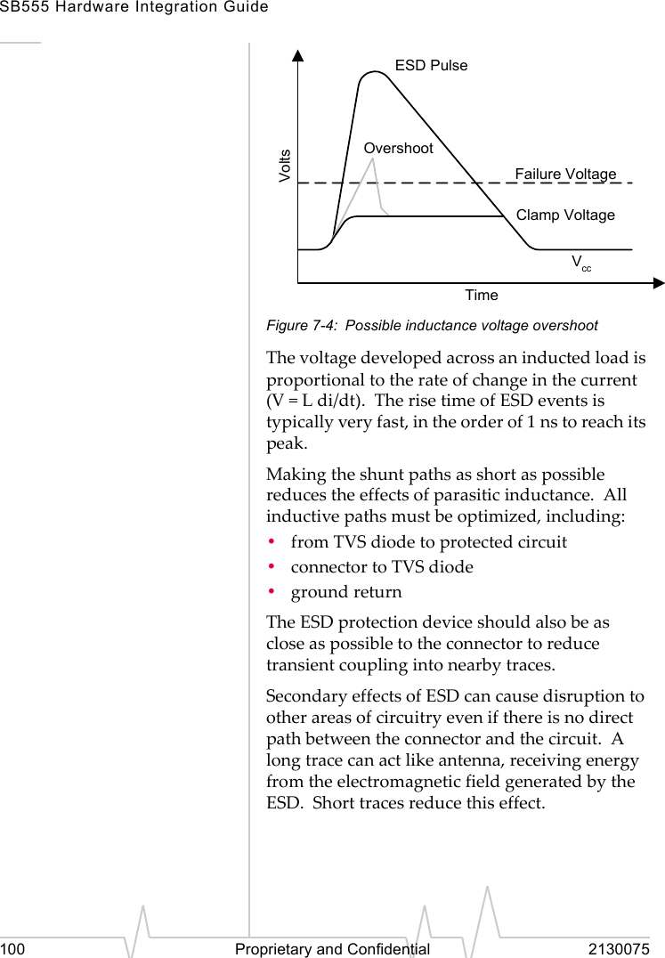
Sierra Wireless SB555 SB555 Embedded Modem Module for Mobile Application User Manual 2130075 Hardware

Sierra Wireless Inc. SB555 Embedded Modem Module for Mobile Application 2130075 Hardware

Contents

User Manual

2130075Rev 1.0SB555Development KitHardware IntegrationGuideProprietary and Confidential
PrefaceRev 1.0  Apr.02   Proprietary and Confidential 1Important NoticeBecause of the nature of wireless communica-tions, transmission and reception of data can never be guaranteed.  Data may be delayed, corrupted (i.e., have errors) or be totally lost.  Although significant delays or losses of data are rare when wireless devices such as the Sierra Wireless modem are used in a normal manner with a well-constructed network, the Sierra Wireless modem should not be used in situations where failure to transmit or receive data could result in damage of any kind to the user or any other party, including but not limited to personal injury, death, or loss of property.  Sierra Wireless, Inc., accepts no responsibility for damages of any kind resulting from delays or errors in data transmitted or received using the Sierra Wireless modem, or for failure of the Sierra Wireless modem to transmit or receive such data.Safety and HazardsDo not operate the Sierra Wireless modem in areas where blasting is in progress, where explosive atmospheres may be present, near medical equipment, near life support equipment, or any equipment which may be susceptible to any form of radio interference.  In such areas, the Sierra Wireless modem MUST BE POWERED OFF.  The Sierra Wireless modem can transmit signals that could interfere with this equipment.Do not operate the Sierra Wireless modem in any aircraft, whether the aircraft is on the ground or in flight.  In aircraft, the Sierra Wireless modem MUST BE POWERED OFF.  When operating, the Sierra Wireless modem can transmit signals that could interfere with various onboard systems.
SB555 Hardware Integration Guide2 Proprietary and Confidential 2130075The driver or operator of any vehicle should not operate the Sierra Wireless modem while in control of a vehicle.  Doing so will detract from the driver or operator's control and operation of that vehicle.  In some states and provinces, operating such communications devices while in control of a vehicle is an offence.Note: Some airlines may permit the use of cellular phones while the aircraft is on the ground and the door is open.  Sierra Wireless modems may be used at this time.Limitation of LiabilityThe information in this manual is subject to change without notice and does not represent a commitment on the part of Sierra Wireless, Inc.  SIERRA WIRELESS, INC. SPECIFICALLY DISCLAIMS LIABILITY FOR ANY AND ALL DIRECT, INDIRECT, SPECIAL, GENERAL, INCIDENTAL, CONSEQUENTIAL, PUNITIVE OR EXEMPLARY DAMAGES INCLUDING, BUT NOT LIMITED TO, LOSS OF PROFITS OR REVENUE OR ANTICIPATED PROFITS OR REVENUE ARISING OUT OF THE USE OR INABILITY TO USE ANY SIERRA WIRELESS, INC. PRODUCT, EVEN IF SIERRA WIRELESS, INC. HAS BEEN ADVISED OF THE POSSI-BILITY OF SUCH DAMAGES OR THEY ARE FORESEEABLE OR FOR CLAIMS BY ANY THIRD PARTY.
PrefaceRev 1.0  Apr.02   Proprietary and Confidential 3Patents Portions of this product are covered by some or all of the following US patents:5,515,013 5,617,106 5,629,960 5,682,6025,748,449 5,845,216 5,847,553 5,878,2345,890,057 5,929,815 6,169,884 6,191,7416,199,168 6,327,154 6,339,405 D367,062D372,248 D372,701 D416,857 D442,170D452,495 D452,496 and other patents pending.This product includestechnology licensed from:Copyright ©2002 Sierra Wireless, Inc.  All rights reserved.Printed in Canada. Tr a d e m a r k s “Heart of the Wireless Machine” is a registered trademark of Sierra Wireless, Inc.Sierra Wireless, the Sierra Wireless logo, the red wave design, and Watcher are trademarks of Sierra Wireless, Inc.Windows® is a registered trademark of Microsoft Corporation.Qualcomm® is a registered trademark of Qualcomm Incorporated.Other trademarks are the property of the respective owners.
SB555 Hardware Integration Guide4 Proprietary and Confidential 2130075Contact InformationYour comments and suggestions on improving this documentation are welcome and appre-ciated.  Please e-mail your feedback todocumentation@sierrawireless.com.  Thank you.Consult our website for up-to-date product descriptions, documentation, application notes, firmware upgrades, troubleshooting tips, and press releases:www.sierrawireless.comSales Desk: Phone: 1-604-232-1488Hours: 8:00 AM to 5:00 PM Pacific Timee-mail: sales@sierrawireless.comTechnical Support: Included with the purchase of the SB555 Development Kit you receive five hours of tier 3 engineering integration support.  You will have received instructions by e-mail on how to access the OEM Customer Support web site.  For more details, please contact your account manager, or the Sierra Wireless sales desk.Post: Sierra Wireless, Inc.13811 Wireless Way,Richmond, BCCanada            V6V 3A4Fax: 1-604-231-1109Web: www.sierrawireless.com
Rev 1.0 Apr.02 Proprietary and Confidential 5Table of ContentsAbout this Guide. . . . . . . . . . . . . . . . . . . . . . . . . . . . . . . . . . . . . . . .   11Introduction  . . . . . . . . . . . . . . . . . . . . . . . . . . . . . . . . . . . . . . . .   11Document structure  . . . . . . . . . . . . . . . . . . . . . . . . . . . . . . . . .   12References . . . . . . . . . . . . . . . . . . . . . . . . . . . . . . . . . . . . . . . . .   13Terminology and acronyms . . . . . . . . . . . . . . . . . . . . . . . .   13Conventions . . . . . . . . . . . . . . . . . . . . . . . . . . . . . . . . . . . . . . . .   13Mechanical Integration . . . . . . . . . . . . . . . . . . . . . . . . . . . . . . . . . .   15Introduction  . . . . . . . . . . . . . . . . . . . . . . . . . . . . . . . . . . . . . . . .   15Physical dimensions . . . . . . . . . . . . . . . . . . . . . . . . . . . . . . . . .   16Mounting the module . . . . . . . . . . . . . . . . . . . . . . . . . . . . . . . .   17Module weight . . . . . . . . . . . . . . . . . . . . . . . . . . . . . . . . . . .   18Module shields  . . . . . . . . . . . . . . . . . . . . . . . . . . . . . . . . . .   18Module connectors . . . . . . . . . . . . . . . . . . . . . . . . . . . . . . . . . .   19Host interface connector . . . . . . . . . . . . . . . . . . . . . . . . . .   19Location of pin 1  . . . . . . . . . . . . . . . . . . . . . . . . . . . . . . . . .   20Antenna connector . . . . . . . . . . . . . . . . . . . . . . . . . . . . . . .   20Assembly sequence  . . . . . . . . . . . . . . . . . . . . . . . . . . . . . . . . .   21Environmental issues . . . . . . . . . . . . . . . . . . . . . . . . . . . . . . . .   21Thermal dissipation  . . . . . . . . . . . . . . . . . . . . . . . . . . . . . .   22Electrostatic discharge. . . . . . . . . . . . . . . . . . . . . . . . . . . .   23Shock and vibration  . . . . . . . . . . . . . . . . . . . . . . . . . . . . . .   24Dust, dirt, and moisture . . . . . . . . . . . . . . . . . . . . . . . . . . .   24
Hardware Integration Guide6 Proprietary and Confidential 2130075Electrical Integration . . . . . . . . . . . . . . . . . . . . . . . . . . . . . . . . . . . . . 25Introduction . . . . . . . . . . . . . . . . . . . . . . . . . . . . . . . . . . . . . . . . . 25Modem specifications  . . . . . . . . . . . . . . . . . . . . . . . . . . . . . . . . 25Location of pin 1 . . . . . . . . . . . . . . . . . . . . . . . . . . . . . . . . . . 26General requirements . . . . . . . . . . . . . . . . . . . . . . . . . . . . . . . . . 27Unused pins. . . . . . . . . . . . . . . . . . . . . . . . . . . . . . . . . . . . . . 27Preventing back-power when the modem is off. . . . . . . . 27Voltage regulation and buffering . . . . . . . . . . . . . . . . . . . . 28Electrostatic discharge  . . . . . . . . . . . . . . . . . . . . . . . . . . . . 29Power  . . . . . . . . . . . . . . . . . . . . . . . . . . . . . . . . . . . . . . . . . . . . . . 29Current consumption . . . . . . . . . . . . . . . . . . . . . . . . . . . . . . 30Sample power integration . . . . . . . . . . . . . . . . . . . . . . . . . . . . . 30Power source . . . . . . . . . . . . . . . . . . . . . . . . . . . . . . . . . . . . . 30MOSFET power switch. . . . . . . . . . . . . . . . . . . . . . . . . . . . . 32Pins 1 and 2: Modem VCC . . . . . . . . . . . . . . . . . . . . . . . . . . 32Power regulator. . . . . . . . . . . . . . . . . . . . . . . . . . . . . . . . . . . 32Pins 3, 4, 25, 30: Ground connection  . . . . . . . . . . . . . . . . . 33Requirements of the power interface. . . . . . . . . . . . . . . . . . . . 34Module shielding  . . . . . . . . . . . . . . . . . . . . . . . . . . . . . . . . . 34Power ramp-up  . . . . . . . . . . . . . . . . . . . . . . . . . . . . . . . . . . . 34Power-up timing . . . . . . . . . . . . . . . . . . . . . . . . . . . . . . . . . . 35Trace widths  . . . . . . . . . . . . . . . . . . . . . . . . . . . . . . . . . . . . . 36
ContentsRev 1.0 Apr.02 Proprietary and Confidential 7Serial Interfaces . . . . . . . . . . . . . . . . . . . . . . . . . . . . . . . . . . . . . . . .   37Introduction  . . . . . . . . . . . . . . . . . . . . . . . . . . . . . . . . . . . . . . . .   37Serial port specifications . . . . . . . . . . . . . . . . . . . . . . . . . .   37External pullup and pulldown resistors . . . . . . . . . . . . . .   38ESD protection. . . . . . . . . . . . . . . . . . . . . . . . . . . . . . . . . . .   39Primary port . . . . . . . . . . . . . . . . . . . . . . . . . . . . . . . . . . . . . . . .   40Pin 21: /DCD1. . . . . . . . . . . . . . . . . . . . . . . . . . . . . . . . . . . .   41Pin 22: RxD1. . . . . . . . . . . . . . . . . . . . . . . . . . . . . . . . . . . . .   41Pin 23: TxD1 . . . . . . . . . . . . . . . . . . . . . . . . . . . . . . . . . . . . .   42Pin 24: /DTR1 . . . . . . . . . . . . . . . . . . . . . . . . . . . . . . . . . . . .   42Pin 25: GND . . . . . . . . . . . . . . . . . . . . . . . . . . . . . . . . . . . . .   43Pin 26: /DSR1 . . . . . . . . . . . . . . . . . . . . . . . . . . . . . . . . . . . .   43Pin 27: /RTS1 . . . . . . . . . . . . . . . . . . . . . . . . . . . . . . . . . . . .   43Pin 28: /CTS1 . . . . . . . . . . . . . . . . . . . . . . . . . . . . . . . . . . . .   44Pin 29: /RI1 . . . . . . . . . . . . . . . . . . . . . . . . . . . . . . . . . . . . . .   44Pin 30: GND . . . . . . . . . . . . . . . . . . . . . . . . . . . . . . . . . . . . .   45Port configuration . . . . . . . . . . . . . . . . . . . . . . . . . . . . . . . .   45Primary port sample integrations . . . . . . . . . . . . . . . . . . .   45Sample 1: Internal host integration  . . . . . . . . . . . . . . . . .   46Sample 2: External serial connector. . . . . . . . . . . . . . . . .   47Sample 3: Minimum integration . . . . . . . . . . . . . . . . . . . .   49Secondary port. . . . . . . . . . . . . . . . . . . . . . . . . . . . . . . . . . . . . .   51Pin 17: /CTS2 . . . . . . . . . . . . . . . . . . . . . . . . . . . . . . . . . . . .   52Pin 18: /RTS2 . . . . . . . . . . . . . . . . . . . . . . . . . . . . . . . . . . . .   52Pin 19: TxD2 . . . . . . . . . . . . . . . . . . . . . . . . . . . . . . . . . . . . .   52Pin 20: RxD2. . . . . . . . . . . . . . . . . . . . . . . . . . . . . . . . . . . . .   53Pin 25: GND . . . . . . . . . . . . . . . . . . . . . . . . . . . . . . . . . . . . .   53
Hardware Integration Guide8 Proprietary and Confidential 2130075Port configuration. . . . . . . . . . . . . . . . . . . . . . . . . . . . . . . . . 53Secondary port sample integration . . . . . . . . . . . . . . . . . . 54Minimum integration . . . . . . . . . . . . . . . . . . . . . . . . . . . . . . 55Voice Interface . . . . . . . . . . . . . . . . . . . . . . . . . . . . . . . . . . . . . . . . . . 57Introduction to voice features . . . . . . . . . . . . . . . . . . . . . . . . . . 57Audio block diagram  . . . . . . . . . . . . . . . . . . . . . . . . . . . . . . 57Pinouts . . . . . . . . . . . . . . . . . . . . . . . . . . . . . . . . . . . . . . . . . . 59ESD protection  . . . . . . . . . . . . . . . . . . . . . . . . . . . . . . . . . . . 59Headset integration  . . . . . . . . . . . . . . . . . . . . . . . . . . . . . . . . . . 60Headset interface specifications  . . . . . . . . . . . . . . . . . . . . 60Microphone input (headset) . . . . . . . . . . . . . . . . . . . . . . . . 62Speaker output (headset)  . . . . . . . . . . . . . . . . . . . . . . . . . . 62Sample headset integration  . . . . . . . . . . . . . . . . . . . . . . . . 62Line level voice integration  . . . . . . . . . . . . . . . . . . . . . . . . . . . . 63Microphone input (line level)  . . . . . . . . . . . . . . . . . . . . . . . 65Speaker output (line level). . . . . . . . . . . . . . . . . . . . . . . . . . 65Control Signals. . . . . . . . . . . . . . . . . . . . . . . . . . . . . . . . . . . . . . . . . . 67Introduction . . . . . . . . . . . . . . . . . . . . . . . . . . . . . . . . . . . . . . . . . 67Control interface specifications . . . . . . . . . . . . . . . . . . . . . 67External pullup and pulldown resistors . . . . . . . . . . . . . . . 68ESD protection  . . . . . . . . . . . . . . . . . . . . . . . . . . . . . . . . . . . 69Status indicators . . . . . . . . . . . . . . . . . . . . . . . . . . . . . . . . . . . . . 69Human interface (LEDs)  . . . . . . . . . . . . . . . . . . . . . . . . . . . 70Sample LED status interface. . . . . . . . . . . . . . . . . . . . . . . . 70
ContentsRev 1.0 Apr.02 Proprietary and Confidential 9Machine interface . . . . . . . . . . . . . . . . . . . . . . . . . . . . . . . .   72Sample machine interface to status outputs  . . . . . . . . .   72Shutdown and reset control. . . . . . . . . . . . . . . . . . . . . . . . . . .   73Pin 37: /Shdn_Ack . . . . . . . . . . . . . . . . . . . . . . . . . . . . . . . .   74Pin 38: /ShutDown  . . . . . . . . . . . . . . . . . . . . . . . . . . . . . . .   74Pin 39: /Reset . . . . . . . . . . . . . . . . . . . . . . . . . . . . . . . . . . . .   75Sample shutdown interface integration  . . . . . . . . . . . . .   76Shutdown sequence . . . . . . . . . . . . . . . . . . . . . . . . . . . . . .   77Shutdown timing. . . . . . . . . . . . . . . . . . . . . . . . . . . . . . . . .   77RF Integration . . . . . . . . . . . . . . . . . . . . . . . . . . . . . . . . . . . . . . . . . .   79Introduction  . . . . . . . . . . . . . . . . . . . . . . . . . . . . . . . . . . . . . . . .   79RF connection  . . . . . . . . . . . . . . . . . . . . . . . . . . . . . . . . . . . . . .   80Connector considerations . . . . . . . . . . . . . . . . . . . . . . . . .   80Ground plane isolation . . . . . . . . . . . . . . . . . . . . . . . . . . . .   81ESD protection. . . . . . . . . . . . . . . . . . . . . . . . . . . . . . . . . . .   82Antenna and cabling . . . . . . . . . . . . . . . . . . . . . . . . . . . . . . . . .   83Matching antenna and cable. . . . . . . . . . . . . . . . . . . . . . .   83Antenna options  . . . . . . . . . . . . . . . . . . . . . . . . . . . . . . . . .   83Cables . . . . . . . . . . . . . . . . . . . . . . . . . . . . . . . . . . . . . . . . . .   84Interference and sensitivity . . . . . . . . . . . . . . . . . . . . . . . . . . .   84Power supply noise . . . . . . . . . . . . . . . . . . . . . . . . . . . . . . .   84Device generated RF. . . . . . . . . . . . . . . . . . . . . . . . . . . . . .   85Modem generated RF switching noise  . . . . . . . . . . . . . .   87
Hardware Integration Guide10 Proprietary and Confidential 2130075Appendix A:Host Connector Pinouts . . . . . . . . . . . . . . . . . . . . . . . . . . . . . . . . . . 89Appendix B:Sample Integration  . . . . . . . . . . . . . . . . . . . . . . . . . . . 93Appendix C:Electrostatic Discharge. . . . . . . . . . . . . . . . . . . . . . . . . . . . . . . . . . . 95Introduction . . . . . . . . . . . . . . . . . . . . . . . . . . . . . . . . . . . . . . . . . 95Charge creation . . . . . . . . . . . . . . . . . . . . . . . . . . . . . . . . . . . . . . 95Damage from ESD. . . . . . . . . . . . . . . . . . . . . . . . . . . . . . . . . . . . 96Types of damage . . . . . . . . . . . . . . . . . . . . . . . . . . . . . . . . . . 97Exposed interfaces . . . . . . . . . . . . . . . . . . . . . . . . . . . . . . . . 97Protection from ESD . . . . . . . . . . . . . . . . . . . . . . . . . . . . . . . . . . 98Requirements  . . . . . . . . . . . . . . . . . . . . . . . . . . . . . . . . . . . . 98TVS diodes . . . . . . . . . . . . . . . . . . . . . . . . . . . . . . . . . . . . . . . 98PCB design  . . . . . . . . . . . . . . . . . . . . . . . . . . . . . . . . . . . . . . 99ESD integration considerations  . . . . . . . . . . . . . . . . . . . . . . . 101Return ground path  . . . . . . . . . . . . . . . . . . . . . . . . . . . . . . 101Capacitance . . . . . . . . . . . . . . . . . . . . . . . . . . . . . . . . . . . . . 102Selection guidelines . . . . . . . . . . . . . . . . . . . . . . . . . . . . . . 103
1Rev 1.0  Apr.02 Proprietary and Confidential 111: About this Guide• Introduction• Document structure• References• Conventions IntroductionThis guide is one component of the SB555 Devel-opment Kit.  It covers the integration of the product from the hardware point of view.  Other guides in the kit cover project planning, software integration, and product verification and config-uration.For details on the features of the SB555 embedded modem, please consult the SB555 Embedded Modem Product Specification (document #2130072).To aid you in making decisions on what aspects of the modem require integration in your project, and to determine what hardware is required to support particular features, please consult the SB555 Development Kit Design Guide (document #2130179).  This hardware guide covers the details of integrating each interface but does not discuss the reasons to include or exclude any particular element.Where configurable features are mentioned, the method of configuring or calibrating can be found in the Verification and Configuration Guide (document #2130078).
SB555 Hardware Integration Guide12 Proprietary and Confidential 2130075Document structureThis document covers hardware integration issues in these main categories:•Mechanical Integration·Mounting·Connectors·Environmental Issues•Electrical Integration·General Specifications·General Considerations·Power Supply·Electrostatic Discharge (ESD)•Serial Interface·Primary Port (Serial 1) - Data·Secondary Port (Serial 2) - Control•Voice Interface·Analog Voice•Control Signals·Status Signals·Shutdown Control·Reset•RF integration·RF Connections·Antenna and Cabling·Interference and Sensitivity•Appendix A—Pinouts•Appendix B—Sample Integration, a typical MCU integration block diagram•Appendix C—Electrostatic Discharge (ESD)
About This GuideRev 1.0  Apr.02   Proprietary and Confidential 13ReferencesThis guide covers only the hardware integration of the SB555 modem.  It does not deal with specifics of product modem operation or use of the optional Embedded Modem Interface Kit.  Please consult the other documents provided with the Development Kit or the Interface Kit User Guide for additional information on opera-tions.You may also want to consult other documents available on our Internet site at www.sierrawireless.com.Terminology and acronymsThis document makes wide use of acronyms that are in common use in data communications and cellular/PCS technology.  Our Internet site provides a Glossary (document 2110032) that may be helpful in understanding some acronyms and terminology used in this guide.ConventionsNumerics Numeric values are generally presented in decimal but may also be expressed in hexadecimal or binary.  Hexadecimal values are shown with a prefix of 0x, i.e. in the form 0x3D.  Binary values are shown with a prefix of 0b, i.e. in the form 0b00111101.  Otherwise, values are presumed decimal.
SB555 Hardware Integration Guide14 Proprietary and Confidential 2130075Units Units of measure are given in metric.  Where measure is provided in imperial units, they are shown in parenthesis after the metric units.Signal Names When signals are discussed by their function, the functional name is used in standard font (i.e. Reset, Shutdown Acknowledge).  When the pin, wire, or trace carrying the signal is referenced, it will use the proper name in an alternate font:/Reset/Shdn_AckSignals that are active low are named with a prefix slash “/” as shown in the sample above.  Signal names without the slash are active high.Fonts Command and register syntax is noted using an alternate font:AT~AUDMOD=1Responses from the modem, or host system software prompts, are shown in this font:CONNECT 14400Character codes which are described with words or standard abbreviations are shown within angle brackets: such as <CR> for Carriage Return and <space> for a blank space character.
2Rev 1.0  Apr.02 Proprietary and Confidential 152: Mechanical Integration• Introduction• Physical dimensions• Mounting• Connectors• Assembly sequence• Environmental issuesIntroductionThe SB555 CDMA2000 1X embedded modem form factor is the proprietary Sierra Wireless embedded module package.  Physical dimen-sions, mounting holes, and connectors are identical to other upcoming Sierra Wireless embedded modem products.This chapter covers the integration issues surrounding:•Mounting•Connector fit•Assembly sequence•Environmental issues
SB555 Hardware Integration Guide16 Proprietary and Confidential 2130075Physical dimensionsThe SB555 comes in the Sierra Wireless propri-etary standard module package.  Dimensions in millimeters are shown in the figure below.Figure 2-1: Module dimensions (in mm)
Mechanical IntegrationRev 1.0  Apr.02   Proprietary and Confidential 17Mounting the moduleNote: The integration should include standoffs of some kind to protect the modem shields from being crushed during assembly and from coming into contact with circuitry on the host device.Sierra Wireless embedded modules have four (4) mounting holes of 2.5 mm (0.984”) diameter, one located at each corner of the module (as seen in Figure 2-1).  The mounting holes are sized to accommodate a metric M2 (#2 screw).The 40-pin host connector allows for either bottom or top entry, to permit mounting in any orientation.  Sierra Wireless does not provide mounting hardware.The sample illustration does not show standoffs.Figure 2-2: Sample bottom entry mounting (mm)
SB555 Hardware Integration Guide18 Proprietary and Confidential 2130075Module weightThe module has a total weight under 14 grams (0.49 ounces).  Typical weight is 13.5 grams (0.48 ounces).Module shieldsThe SB555 comes with shields on both top and bottom.  These shields are attached to a fence surrounding the circuitry.Figure 2-3: Shield fence frameThe internal webbing of the fence frame may be removed in some units to permit factory rework.  This webbing is used for automated pick-and-
Mechanical IntegrationRev 1.0  Apr.02   Proprietary and Confidential 19place only.  The product has been fully qualified mechanically and electrically with and without the webbing.Module connectorsThere are two connectors: a 40-pin header for the host interface, and an MMCX connector for the antenna.  Both are mounted offset from the module centerline to prevent assembly orien-tation errors.Host interface connectorThe host connector is a 40-pin, 1 mm pitch, 2-row, female header (Samtec part #CLM-120-02-F-n-BE with bottom entry option).  This host connector is capable of accepting either a top or bottom entry mating header connector.Suitable mating connectors are:•Samtec (www.samtec.com) MW, FTM or FTMH series•Major League Electronics(www.majorleagueelectronics.com) BSTCM-7 seriesThe recommended exposed pin length is:•1.4 mm (0.055”) for top entry•3.2 mm (0.125”) for bottom entryThe connector is not keyed.  The connector is offset from the module centerline to prevent assembly orientation errors.
SB555 Hardware Integration Guide20 Proprietary and Confidential 2130075Location of pin 1Pin 1 of the host connector is shown in Figure 2-4.  When viewing the module with the connector facing up and the RF connector at the bottom, pin 1 is on the extreme right of the inside edge (lower row).Figure 2-4: Host connector pin locationsAntenna connectorThe antenna connector is an MMCX female jack oriented in line with the module longitudinal axis.  Mating plugs can be either straight or right-angle.The detent on the connector is quite stiff to ensure the connection remains intact through vibration and shock.  The connector is designed for 500 connection cycles, which may not be sufficient for some end-user applications.  For this reason, and to allow for ESD protection, the modem’s MMCX connector should not be presented directly to the user for antenna attachment.The integration can include a host system built-in antenna—without presenting a connector to the user—or any of a variety of RF connector types (SMA, SMB, TNC, etc.) as suits the application.  See “Ground plane isolation” on page 81 for additional information on insulating the RF connector ground.Pin 1Pin 2Pin 19Pin 39Pin 40
Mechanical IntegrationRev 1.0  Apr.02   Proprietary and Confidential 21For mechanical integration, use a flexible 50 Ω coaxial cable to allow attachment of the MMCX connector to the modem either before or after mounting the module on the host device.Assembly sequenceDue to the strong detent in the MMCX antenna connector, Sierra Wireless recommends that you connect the antenna cable to the modem before connecting the modem’s 40-pin connector to the host device.  This will avoid stress on the host connector.  Your situation may vary; this is only a recommendation.  Where host mounting is performed prior to antenna cable attachment, the module should be secured, with screws and standoffs, to the host device.Use suitable standoffs with screws or other mounts to hold the module securely in place, while preventing the modem’s shield from grounding to the host device.Environmental issuesThe SB555 embedded modem conforms to the specifications listed in Table 2-1 on the following page.  Enhanced specifications may be achieved through appropriate mounting.
SB555 Hardware Integration Guide22 Proprietary and Confidential 2130075Thermal dissipationDetermination of thermal dissipation depends heavily on the usage model of the modem.  The SB555 modem generates more heat when actively transmitting.  However the transmitter is not on at all times, nor is the transmit power constant.Table 2-1: Environmental specificationsTemperature range Operating: -30 to +60°C (-22 to +140°F)(modem ambient*)Storage: -40 to +85°C (-40 to +185°F)Humidity MIL-STD-202F95% non-condensing @ 65°C (149°F)Vibration (random)**MIL-STD-810E0.04 g2/Hz, 10 – 2000 HzVibration(sine wave)**PC Card Standard15 g (147 m/s2), 10 – 2000 HzShock** MIL-STD-202F50 g (490 m/s2), 11 ms, 6 pulses/axisDrop** (unpackaged)PC Card Standard0.75 meter drop onto non-cushioned vinyl(2 drops on each axis, 6 drops total)* Modem ambient means in the immediate area of the modem, not the ambient temperature around the finished device.  This is typically a temperature inside your device.A thermistor inside the modem (monitored by the modem CPU firmware) causes flow control to be activated should the internal temperature reach 75ºC (167ºF) as measured at the radio.  Flow control is released when the temperature falls below 75ºC.  Should the temperature of the radio reach 80ºC (176ºF), the modem terminates the connection in order to protect com-ponents and avoid drifting outside radio specifications.** Vibration, shock, and drop tests are performed for survivability.  The modem is not in operation during the test.  Cosmetic damage is ignored.
Mechanical IntegrationRev 1.0  Apr.02   Proprietary and Confidential 23Table 2-2 provides a guideline of the energy to be dissipated when the modem is in various states of activity.Transmit cases are usually short duration bursts.Electrostatic dischargeThis is treated as an electrical integration issue.  The SB555 does not provide a specified level of protection from electrostatic discharge (ESD).  Exposed interfaces should be protected by your circuitry design.  Details are covered in Chapter 3:Electrical Integration.Consult “Electrostatic Discharge” on page 95 for a general discussion of ESD.Table 2-2: Energy dissipation (typical)Mode Current consumptionEnergy to dissipateShutdown 3.3 V @ 0.7 mA 2.3 mWSlotted sleep (SCI = 2) (DTR deasserted)3.3 V @ 5 mA 16.5 mWSlotted sleep (SCI = 2) (DTR asserted)3.3 V @ 40 mA 132 mWReceive 3.3 V @ 160 mA 528 mWTransmit(typical at +3 dBm)3.3 V @ 370 mA 1219 mWTransmit (worst case)(full power +23.5 dBm)4.2 V @ 900 mA 3376 mW
SB555 Hardware Integration Guide24 Proprietary and Confidential 2130075Shock and vibrationThe specifications provided on shock and vibration are for the module free of integration hardware.A person rolling off a bed onto the floor is likely to emerge without injury; whereas one with a fire hydrant strapped to his back may not.  Once integrated into your device, the surrounding hardware can have a significant impact on the modem’s survivability.Through the mounting and integration decisions you make, your design will need to meet your own product’s survivability specifications.Dust, dirt, and moistureThe shields are not intended to provide the modem with protection from dust, dirt, or moisture.  Your integration should provide reasonable insulation from these environmental factors as needed to meet your product’s specifi-catons.
3Rev 1.0  Apr.02 Proprietary and Confidential 253: Electrical Integration• Introduction• Specifications• General requirements• Power supply• Electrostatic dischargeIntroductionThis chapter covers the integration requirements and issues related to the general electrical connection of the SB555 modem, and the power supply in particular.  RF issues are covered in Chapter 7:RF Integration on page 79.The SB555 embedded modem presents all electrical interfaces on the single 40-pin host connector.  This chapter covers:•The connector and the general electrical characteristics of the modem•Power supply considerations•Electrostatic Discharge (ESD) protectionThe elements of integrating each of the modem interfaces (serial, voice, and control signals) are covered in subsequent chapters.Modem specificationsThe SB555 embedded modem provides a single 40-pin (2x20) header.  The connector pinouts are specified in Appendix A:Host Connector Pinouts on page 89.All signals are 3.0 V, HCMOS logic compatible.
SB555 Hardware Integration Guide26 Proprietary and Confidential 2130075Location of pin 1Pin 1 of the connector is shown in Figure 3-1.  When viewing the module with the connector facing up and the RF connector at the bottom, pin 1 is on the extreme right of the inside edge (lower row).Figure 3-1: Host connector pin locationsTable 3-1: Host interface electrical characteristicsParameter Test Conditions Min Typical Max UnitsPowerVcc DC supply Max ripple 100 mVp-p 3.2 3.3 4.2 VDigital InterfaceVIH HI threshold 2.1 3.0 3.3 VVIL LO threshold 0 0 0.8 VIIH Input current 3 V applied to input 0120 µAIIL Input current 0 V applied to input 0-120 µAVOH HI output IOH = 2.0 mA 2.4 3.0 VVOL LO output IOL = -2.0 mA 00.4 VIOH Output currentVOH > 2.0 V 3.0 mAIOL Output currentVOL < 1.0 V -3.0 mAPin 1Pin 2Pin 19Pin 39Pin 40
Electrical IntegrationRev 1.0  Apr.02   Proprietary and Confidential 27General requirementsUnused pinsUnused signals must be terminated properly.   The pinout tables, both in the Appendix and in the interface sections, include a column for termi-nation of unused pins.Preventing back-power when the modem is offNote: Without proper input protection, the modem may draw sufficient current to remain powered, even when the normal supply power is removed.Active low signals may be deasserted (driven high) by the host device when the modem is not needed.  This applies 3.0 V to the modem on these pins and presents the risk of back-powering.All connector inputs must be either high impedance (>20 kΩ), or driven low, when the modem is powered off.  This is required to prevent back-powering the modem.  This is particularly important if the DTR signal is deasserted (high) when the modem is not in use.The sample integration shown in the appendix uses buffers.  These provide both voltage conversion between 3.0 V of the modem and 3.3 V of the host MCU, and the required protection from back powering both the MCU and the modem.
SB555 Hardware Integration Guide28 Proprietary and Confidential 2130075Voltage regulation and bufferingAll logic signals at the SB555 host connector are referenced to 3.0 V.  Logic signals at the host device may be referenced to 3.3 V, thus requiring the use of buffers between the devices.  These buffers are discussed in the sections on the specific interfaces.  See the Typical MCU Integration block diagram in the appendix.Note: The actual VCC of the logic internal to the SB555 is 3.0 V, not the 3.2 V–4.2 V applied to the VCC pins of the SB555 module.  The 74AHC series parts can tolerate 3.3 V applied to inputs while VCC =0V.This buffer is mainly to protect the SB555 when it is powered down while the host device remains powered up.Additionally, the modem’s input pins should not have a voltage applied to them that is more than 0.3 V above the internal VCC, which could happen when the modem is powered down.Although some of the SB555 output lines are configured as inputs by a reset, they all have weak internal pullup or pulldown devices (approx. 50 k to 375 kΩ), so no external resistors need to be added.  If you decide to add external resistors:•Use pulldown resistors for:· /RI1·/DCD1•Use pullup resistors (to 3.0 V) for:·/DSR1·/CTS2·RxD2·/Shdn_AckThis is consistent with the internal devices.  A suggested value is 100 kΩ.
Electrical IntegrationRev 1.0  Apr.02   Proprietary and Confidential 29Note: Floating signal lines can be noisy, and increase power consumption.If a host reset configures any of its I/O pins (controlling outputs to the modem: DTR1, /RTS1, TxD1, /RTS2, TxD2, /ShutDown, MdmReset) as an input, and the pin does not have any internal pullup or pulldown device, use a pulldown resistor to prevent the line from floating.  A suggested value is 100 kΩ.Electrostatic dischargeYou are responsible for any ESD protection on digital circuits.  Specific recommendations are provided as needed for each of the interfaces described in this guide.  An appendix (page 95) also provides background on ESD.PowerThe SB555 CDMA2000 1X embedded modem requires 3.2—4.2 VDC (+3.3 V nominal); suitable for direct connection to a lithium-ion battery.  The modem uses the following pins for the power interface:Table 3-2: Power pinoutsPin Name Description Type Termination if not used1, 2 Vcc 3.3 VDC power supply Power Required3, 4 GND Ground Power Required25 GND Ground Power Required30 GND Ground Power Required
SB555 Hardware Integration Guide30 Proprietary and Confidential 2130075Pins 25 and 30 are included to provide a connection to ground near the pins for the two serial ports.The electrical characteristics of the power supply are:•Max ripple: 100 mVp-p (1 Hz – 100 kHz)•Minimum: 3.20 V•Typical: 3.30 V•Maximum: 4.20 VCurrent consumptionThe current consumption of the modem varies considerably on the usage model of your device.  Consult the Design Guide (document #2130179) for assistance in planning your requirements.Sample power integrationThe integration is discussed with reference to the sample block diagram in Figure 3-2: Power interface block diagram on page 31.  All samples assume an MCU running at 3.3 V.  If your host device uses internal logic at 3.0 V then the buffers discussed in this document may not be needed.Power sourceIn the sample, the power source is a lithium-ion battery.  Your power source may differ provided you stay within the 3.20–4.2 VDC requirement.  The power is shown independent of the host device (MCU) power source, which may differ in your integration.
Electrical IntegrationRev 1.0  Apr.02   Proprietary and Confidential 31For the SB555 modem to maintain a clean RF signal, it is essential that the power supply also be clean.  Ensure the supply power is as free of noise as possible.Figure 3-2: Power interface block diagram
SB555 Hardware Integration Guide32 Proprietary and Confidential 2130075MOSFET power switchNote: This mechanism is needed to follow the recommended shutdown sequence prior to removing power from the modem.The MOSFET power switch is recommended to provide the host device with software control of the power to the SB555 modem.  A suggested part is SI2305DS from Siliconix (www.vishay.com/brands/siliconix/).If an MCU reset configures the I/O pin that  controls the MOSFET switch as an input, use a pullup or pulldown resistor to default the MOSFET control signal to the off state.Pins 1 and 2: Modem VCCTo support a short burst power surge (current draw) when the module’s transmitter is turned on, the power supply is filtered by a 100 µF low-ESR (Equivalent Series Resistance) capacitor between the supply (VBATT) and ground.  Locate this as close as possible to the module connector.If a tantalum capacitor is used, it must have a sufficient surge current rating to handle a low-impedance current source like a battery, otherwise it could fail.Power regulatorThis regulator is used to provide the appropriate voltage (3.0 V) for the LEDs and the digital signal input buffer.  However, if the source power supply (VBATT) never exceeds 3.30 V, this voltage regulator can be omitted, the LED resistors can be connected directly to VBATT, and the buffer can also be powered directly by VBATT.
Electrical IntegrationRev 1.0  Apr.02   Proprietary and Confidential 33If the LEDs were connected directly to a VBATT of 4.2 V, the voltage at the /Status pins could exceed the limit of  VCC + 0.3 V, possibly damaging the modem.  There could also be constant leakage current, draining the battery.  This will depend on the voltage drop across the selected LEDs.Similarly, if the buffer were powered by a VBATT greater than 3.30 V, the voltage at the input pins of the SB555 would also exceed the VCC + 0.3 V limit.Use a 3.0 V low-dropout (LDO) voltage regulator of sufficient output current to provide power to the I/O buffers (and LEDs if needed).  A suggested part is the LP3985-3.0 from National Semiconductor.Pins 3, 4, 25, 30: Ground connectionThe ONLY ground connection to the modem must be through the 40-pin host connector.  No ground connection to the modem shields must be made.  This is to avoid degrading the RF perfor-mance of the modem through ground loops.Also consult the section: Ground plane isolation on page 81.
SB555 Hardware Integration Guide34 Proprietary and Confidential 2130075Requirements of the power interfaceModule shieldingThe module is fully shielded to protect against EMI and to ensure FCC regulatory compliance.  To maintain the shield effectiveness the modem shields must not be removed and must not be connected to the host ground.Ground loops must be avoided.  See “Ground plane isolation” on page 81.Power ramp-upThe SB555 modem will hold the circuitry in reset until stable power is established.  When the voltage reaches 2.7 V nominal (2.55–2.925 V) and is held at or above that level for at least 10 µs, a timer is started.  The modem continues to hold in reset for 140–560 ms to ensure power is stable.  If power slips below 2.7 V for a few micro-seconds, the timer must restart.Figure 3-3: Power ramp-up timing
Electrical IntegrationRev 1.0  Apr.02   Proprietary and Confidential 35Power-up timingAfter release from reset, the modem performs a self test and initialization.  It begins normal operation within 7–15 seconds.All serial port signals should be considered undefined or invalid until both /DSR1 and /CTS1 are asserted.  Only at that time is the modem ready for use.Figure 3-4: Control signal timing•t0—Reset is released.•t1—After self test, initialization begins./DCD1 may change state based on its condition at the time of the reset.  It should be ignored.•t2—/DSR1 asserts.  Other signals should still be considered invalid.•t3—/CTS1 asserts, typically 156 µs after /DSR1.  At this time, the modem is ready.Note: /DCD1 is shown in its factory default configuration.Signals other than /DSR1 and /CTS1 should be considered invalid or undefined until the process is complete.  The final state of /DCD1 will depend on its configuration.
SB555 Hardware Integration Guide36 Proprietary and Confidential 2130075Trace widthsEnsure that the PCB trace widths to the SB555 VCC and GND pins are sufficient for a maximum current of 900 mA.  Consult the Design Guide (document #2130179) for details on current consumption in all modes.Do not connect the modem package shield to GND or AGND.
4Rev 1.0  Apr.02 Proprietary and Confidential 374: Serial Interfaces• Introduction• Primary port• Secondary port IntroductionThe SB555 CDMA2000 1X embedded modem presents two serial port interfaces.•Primary port—the basic modem interface offering AT command and user data I/O•Secondary port—for modem management using a Sierra Wireless proprietary CnS (Control and Status) protocolThis chapter deals with the electrical integration of each of these two serial ports.  A full integration of both ports is recommended but a reduced integration is possible if you are prepared to sacrifice some features.  Consult the Design Guide (document #2130179) for a discussion of the issues related to excluding connection of specific signals.Serial port specificationsThe serial ports operate at the same 3.0 V, HCMOS level as the rest of the modem’s digital interfaces, not +/-12 V RS-232C levels.If a modem serial port is to be presented to the user, appropriate level conversion and ESD circuitry is required.
SB555 Hardware Integration Guide38 Proprietary and Confidential 2130075External pullup and pulldown resistorsAlthough some of the SB555 output lines are configured as inputs by a reset, they all have weak internal pullup or pulldown devices (approx. 50 K to 375 kΩ), so no external resistors need to be added.  If you decide to add external resistors (suggested value is 100 kΩ), to be consistent with the internal devices:•Use pulldown resistors for:·/RI1·/DCD1•Use pullup resistors (to 3.0 V VBUF) for:·/DSR1·/CTS2·RxD2Table 4-1: Serial interface electrical characteristicsParameter Conditions Min Typ. Max UnitsDigital InterfaceVIH HI threshold 2.1 3.0 3.3 VVIL LO threshold 00.8 VIIH Input current 3 V applied input 10 120 µAIIL Input current 0 V applied input 0-120 µAVOH HI output IOH = 1.0 mA 2.0 3.0 VVOL LO output IOL = -1.0 mA 00.4 VIOH Output currentVOH > 2.0 V 3.0 mAIOL Output currentVOL < 1.0 V 0-3.0 mA
Serial InterfacesRev 1.0  Apr.02   Proprietary and Confidential 39If integrating to an MCU, and its reset configures any of its I/O pins (controlling outputs to /DTR1, /RTS1, or TxD1) as an input, and the pin does not have any internal pullup or pulldown device, use a pulldown resistor to prevent the line from floating.  Floating signal lines can be noisy, and increase power consumption.  A suggested value is 100 kΩ.ESD protectionYou are responsible for any ESD protection on digital circuits.If you plan to extend one or both serial ports to the outside, choose a transceiver capable of 3.3 V logic and with built-in ESD protection.  Suggested parts include:•SIPEX (www.sipex.com) SP3238E•Maxim (www.maxim-ic.com) MAX3238E or MAX3222E•Texas Instruments (www.ti.com) MAX3238
SB555 Hardware Integration Guide40 Proprietary and Confidential 2130075Primary portThe primary serial port pins (Serial 1) comprise a standard set of serial data and handshaking (control) lines.  Signals must be terminated properly if they are not used.At a minimum, the integration requires RxD, TxD, and GND.  The modem is not capable of ignoring RTS/CTS flow control.  If these signals are not used in your integration, then /RTS1 must be forced active (low, grounded) when the modem is powered.Table 4-2: Primary Port (1) Connector PinoutsPin Name Description Type Termination if not used21 /DCD1 Serial 1 – DCD Output Not connected22 RxD1 Serial 1 – RX Output Required23 TxD1 Serial 1 – TX Input Required24 /DTR1 Serial 1 – DTR Input Ground25 GND Ground Power Required26 /DSR1 Serial 1 – DSR Output Not connected27 /RTS1 Serial 1 – RTS Input Ground28 /CTS1 Serial 1 – CTS Output Not connected29 /RI1 Serial 1 – RI Output Not connected30 GND Ground Power Required
Serial InterfacesRev 1.0  Apr.02   Proprietary and Confidential 41Note: If your application intends to use Windows ACPI, then both DTR and RI are required signals.The remaining primary port control lines (DCD, DTR, DSR, and RI) are, strictly speaking, not needed; however they are desirable in most applications.The SB555 modem is designed to use all control signals of the serial interface.  The recommended integration is to use the full family of controls to provide the greatest functionality.Pin 21: /DCD1Data Carrier Detect normally asserts when the modem is on a traffic channel.  It can be configured to:•Behave in a Unix-style “wink” mode—on at all times and wink off (~1 s) when the traffic channel is lost•Reflect the state of the connection—on when connected and off when disconnected•Always assertThe configuration method is discussed in the Verification and Configuration Guide (document #2130078).Although not required, it is recommended to use DCD.  If not used, the pin is left unconnected.Pin 22: RxD1This is the data channel from the modem (network) to the host.  This is a required pin in all integrations.
SB555 Hardware Integration Guide42 Proprietary and Confidential 2130075Pin 23: TxD1This is the data channel from the host to the modem (network).  This is a required pin in all integrations.Pin 24: /DTR1Data Terminal Ready is used extensively to control modem operations as discussed in the Design Guide.  This pin is not strictly required, although it is required for Windows ACPI.If DTR is not used in your integration, /DTR1 must be tied active (low) by connecting to ground.The sample integration in the appendix (page 93) shows the /DTR1 line being driven by an open drain device (for example, a TMOS FET such as the 2N7000 or 2N7002), with a pulldown resistor on the input gate of the FET.The MCU I/O pin driving the /DTR1 signal should be high-impedance (or input), or an output driven to 0 V during and immediately after MCU reset.  This allows the modem to remain in shutdown mode if the host’s DTR pin was deasserted to request the shutdown, and the MCU is subsequently powered down, then powered up again.This FET also protects the MCU when it is powered down while the modem remains powered up.  The modem’s /DTR1 pin has a pullup resistor which could cause the voltage on the MCU pin to exceed VCC + 0.3 V, back-power the MCU, and increase the drain on the modem’s battery.  This device prevents these problems.
Serial InterfacesRev 1.0  Apr.02   Proprietary and Confidential 43The SB555 is also protected by this FET when the modem is powered down while the MCU remains powered up.  The modem’s input pins should not have a voltage applied to them that is more than 0.3 V above VCC, which could otherwise happen when the modem is powered down.Pin 25: GNDThis is a signal ground made available in proximity to the other serial port pins for conve-nience.Pin 26: /DSR1Data Set Ready is normally asserted following successful completion of a modem’s self-test and initialization.  DSR is deasserted when the modem is in shutdown state, to advise the host that it is not available for use.DSR is optional but recommended.  If not used, it can be left unconnected.Pin 27: /RTS1Request To Send is asserted by the host when it is capable of receiving data from the modem, and deasserted to prevent overflow.The modem cannot ignore RTS, so if it is not used, it must be tied active (low) by connecting to ground; however doing this will risk data overflow at the host device.
SB555 Hardware Integration Guide44 Proprietary and Confidential 2130075Pin 28: /CTS1Clear To Send is asserted by the modem when it is capable of receiving data from the host, and deasserted when the modem’s buffers are full (or the modem is not ready to receive commands from the host).This pin is also the final signal to the host indicating that the modem has completed its initialization and is ready for use.Only if the application can tolerate data loss due to transmission overruns, should this pin can be left unconnected.Pin 29: /RI1Ring Indicator is used to advise the host of one of the following conditions:•An incoming call (telephone is ringing)•An incoming SMS message•A return to network coverageWindows ACPI requires use of this signal.  Otherwise, the signal is optional.  If not used, it can be left unconnected.RI is strongly recommended for any integration using the voice feature of the modem.  The RI signal can be used to wake a sleeping host when an incoming call arrives, allowing the device to perform much like a standard cellular telephone.If RI is used for wakeup, you must connect it to an appropriate circuit to detect it and manage the host wakeup operation./RI1 is an active low signal that asserts with a duty cycle of 200 ms on and 200 ms off.  Incoming calls will trigger the RI to cycle until
Serial InterfacesRev 1.0  Apr.02   Proprietary and Confidential 45the connection attempt is either answered or dropped.  The other event triggers (SMS messages and return to coverage) will assert /RI1 three times for each triggering event.Your implementation must handle the detection of events and ignore any additional cycles that are not needed.Pin 30: GNDThis is a signal ground made available in proximity to the other serial port pins for conve-nience.Port configurationThe primary serial port is configured for 8-data bits, no parity bits, and 1-stop bit.  The DTE host data-rate on the primary serial port can be from 9600 bps to 230.4 kbps, configured by software command.  The factory default setting is 115.2 kbps.The modem does not support autobaud detection.Primary port sample integrationsThree integration options are discussed below:•Internal host integration connects to a serial port of an MCU•External serial connector exposing a standard RS-232 connection•Minimum integration, the minimal connection (to an MCU in this sample).
SB555 Hardware Integration Guide46 Proprietary and Confidential 2130075Sample 1: Internal host integrationThis sample integrates all signals of the serial port to an MCU.Buffers are used to manage the level conversions between 3.0 V at the modem and 3.3 V at the MCU.  SN74AHC541 (or equivalent) octal buffers powered by a 3.0 V (VBUF) rail will serve on the inputs to the modem.  Connect the /OE1 and /OE2 buffer pins to GND.Connect the inputs of any unused buffers to GND and leave the outputs unconnected.Another SN74AHC541 (or equivalent) octal buffer, this time powered by the host's 3.3 V (VCC) rail, is used to protect the output lines from the modem.The source of the 3.0 V VBUF power used by the input buffer is discussed in the section: Power regulator on page 32.  The output buffer is powered by the host’s supply.Figure 4-1: Primary serial port integration—MCU Sample
Serial InterfacesRev 1.0  Apr.02   Proprietary and Confidential 47This sample uses an open drain on /DTR1, which is discussed in the description of Pin 24: /DTR1 on page 42.If the host will be using partial system shutdown to conserve power—relying on the modem to wake up the host via the ring indicator—then the /RI pin at the MCU will have to be an interrupt-capable input to trigger the host wakeup.Sample 2: External serial connectorIf you are going to present the primary serial port as an external RS-232 interface, you must include appropriate level conversion and ESD protection.  Typically a MAX3238 is used, as shown in Figure 4-2.The supply power to the chip must be the same 3.0 V (VBUF) level supported by the digital logic of the SB555.  This ensures the output signals from the RS-232 conversion do not over drive the SB555.If the host system logic is used to enable the conversion chip (as shown in the sample), the same logic should control the power to the SB555 (although not shown in the sample).  This prevents a situation where the conversion chip might back-power the SB555 through /DTR1 and /RTS1.  Conversely, if the SB555 is powered while the MAX3238 is not, there can be a current drain through the SB555 serial outputs.Values for the capacitors are not shown.  Consult the data sheet for the chip you use for values.
SB555 Hardware Integration Guide48 Proprietary and Confidential 2130075Figure 4-2: Primary serial port integration—external RS-232 connectorDepending on the capabilities of the selected chip, the ring indicator may still be used to control host power.  Provided the 3.0 V supply is active and the software switch is off, the chip may still pass the /RI1 signal to another pin (not shown) that can be used to wake the local host.
Serial InterfacesRev 1.0  Apr.02   Proprietary and Confidential 49Sample 3: Minimum integrationAt a minimum, data receive (RxD1) and transmit (TxD1), and ground (GND) are required.  This sample integration does not enforce flow control so data overruns and lost data are possible; your application must be tolerant of this.The minimum required integration is described in Table 4-3 and the block diagram in Figure 4-3:Table 4-3: Primary port minimum integrationSignal Pin Requirement/DCD1 21 Optional (unconnected)RxD1 22 RequiredTxD1 23 Required/DTR1 24 GNDGND 25 GND/DSR1 26 Optional (unconnected)/RTS1 27 GND/CTS1 28 Optional (unconnected)/RI1 29 Optional (unconnected)GND 30 GND
SB555 Hardware Integration Guide50 Proprietary and Confidential 2130075Figure 4-3: Primary serial port integration—minimum sampleNote: The modem is not capable of ignoring RTS/CTS flow control.  If these signals are not used in your integration, then RTS must be forced active (low) when the modem is powered.The modem firmware always respects hardware handshaking.  This means that if RTS/CTS are not used, the /RTS1 signal input to the modem must be forced active (low) by connecting it to ground.The CTS signal is optional and can be left uncon-nected if not used.  The modem will assert and deassert it regardless of the hardware integration.DTR can be configured for a variety of control applications in the modem.  To prevent accidental recognition of transitions and avoid any flow control problems, the required integration of an unused /DTR1 signal is to tie it active (low) by connecting to ground.All other control lines are outputs from the modem and can be safely left unconnected if not needed.
Serial InterfacesRev 1.0  Apr.02   Proprietary and Confidential 51Secondary portNote: This port is required for operation with Watcher, the Sierra Wireless enabling software.The secondary port of the SB555 embedded modem is used to exchange control and status information while a data connection is in progress on the primary port.  The secondary port can also support CAIT—a diagnostics tool—used during CDG3 testing.The port is, strictly speaking, optional, but without it, the host device is very limited in its ability to control or monitor the modem while connected.  See the Design Guide (document #2130179) for a full discussion.This port provides only the basic TX and RX lines along with flow control—RTS and CTS.  Other control signals are not provided.Table 4-4: Secondary port connector pinoutsPin Name Description Type Termination if not used17 /CTS2 Serial 2 – CTS Output Not connected18 /RTS2 Serial 2 – RTS Input Ground19 TxD2 Serial 2 – TX Input Ground20 RxD2 Serial 2 – RX Output Not connected25 GND Ground Power Required
SB555 Hardware Integration Guide52 Proprietary and Confidential 2130075Pin 17: /CTS2The Clear To Send signal is optional and can be left unconnected if not used.  The modem will assert and deassert it regardless of the hardware integration.Clear To Send is asserted by the modem when it is capable of receiving CnS commands from the host, and deasserted when the modem’s buffer is full (or the modem is not ready to receive CnS commands from the host).Only if the application can tolerate loss of CnS commands due to transmission overruns, should this pin be left unconnected.Pin 18: /RTS2Request To Send is asserted by the host when it is capable of receiving CnS responses and notifica-tions from the modem, and deasserted to prevent overflow.The modem cannot ignore RTS, so if it is not used, it must be tied active (low) by connecting to ground.Pin 19: TxD2Note: See the Design Guide for details of the consequences of not including the secondary port in your integration.This is the data channel from the host to the modem for CnS messages.  This is a required pin in all integrations using Watcher; otherwise the pin is optional.
Serial InterfacesRev 1.0  Apr.02   Proprietary and Confidential 53Pin 20: RxD2This is the data channel from the modem to the host for CnS messages and notifications.  This is a required pin in all integrations using Watcher; otherwise it is optional.Pin 25: GNDThis is a signal ground made available in proximity to the other serial port pins for conve-nience.Port configurationThe secondary serial port is configured for 8-data bits, no parity bits, and 1-stop bit.  The DTE host data-rate on the secondary serial port can be from 9600 bps to 115.2 kbps, configured by software command.  The factory default setting is 115.2 kbps.The modem does not support autobaud detection.
SB555 Hardware Integration Guide54 Proprietary and Confidential 2130075Secondary port sample integrationNote: The secondary port is typically not extended to an outside RS-232 connector, although this can be done in a completely standalone modem product—one not using built-in host application software.This sample integrates all signals of the serial port to an MCU.Buffers are used to manage the level conversions between 3.0 V at the modem and 3.3 V at the MCU.  This element of the integration is the same as that described on page 46 for the primary port.The source of the 3.0 V (VBUF) power used by the input buffer is discussed in the section: Power regulator on page 32.  The output buffer is powered by the host’s supply.Figure 4-4: Secondary serial port sample integration
Serial InterfacesRev 1.0  Apr.02   Proprietary and Confidential 55Minimum integrationTo use the port, the minimum integration is described in the following table:Figure 4-5: Secondary serial port minimum integrationAt a minimum, receive (RxD2) and transmit (TxD2) data, along with ground (GND) are required.  This integration does not enforce flow control so data overruns and lost data are possible; your application must be tolerant of this.Table 4-5: Secondary port minimum integrationSignal Pin Requirement/CTS2 17 Optional/RTS2 18 GNDTxD2 19 RequiredRxD2 20 RequiredGND 25 Required
SB555 Hardware Integration Guide56 Proprietary and Confidential 2130075
5Rev 1.0  Apr.02 Proprietary and Confidential 575: Voice Interface• Introduction• Headset• Line level Introduction to voice featuresThe SB555 CDMA2000 1X embedded modem supports voice operation similar to a cellular telephone.  Integration of the modem to use the voice features requires a microphone input and speaker output.  These can be either directly to a standard cellular headset or to your custom audio circuit (at line level).The modem’s analog voice capability is configured at the factory to use a direct connection to a standard cellular headset.  Software commands are used to make configu-ration and calibration changes.This chapter has sections describing each of the two configurations of the voice interface.Audio block diagramThe simplified block diagram on the following page is intended to provide you with some understanding of how the various configuration, calibration, and user controls affect the circuit.The AT commands used to control the audio circuit are all prefixed with the tilde (~) character.There are two areas where a loopback can be configured for testing (not shown), that are described in the Verification and Configuration Guide.
SB555 Hardware Integration Guide58 Proprietary and Confidential 2130075Figure 5-1: Simplified audio block diagramSetting line level (~AUDMOD) primarily affects the amount of microphone gain.  There is also some associated filtering, used to compensate for the headset microphone, that will be switched out (flat response) when using the line level configuration.Calibration of the microphone and speaker levels is handled on the digital side of the Codec.  Use of ~MICLVL and ~SPKLVL is described in the Configuration and Verification Guide.The user’s volume control (~SPKVOL) is prior to the echo cancellation circuitry.  It is also included in the sidetone return, along with a separate control of sidetone gain (~STGLVL).
Voice InterfaceRev 1.0  Apr.02   Proprietary and Confidential 59PinoutsNote: The Audio Common Ground is independent of the system’s signal ground.If the audio circuitry is not used, the inputs (pins 13 and 15) should be connected to AGND (pin 16).  Under normal operation, the modem only turns on the audio circuit when needed for a voice connection.  Note that if the audio circuit is enabled, there is a bias current of just under 1 mA on the MIC pins that will cause some current drain.ESD protectionYou are responsible for any ESD protection required.  An appendix (page 95) provides background on ESD.Table 5-1: Analog voice interface pinoutsPin Name Description Type Termination if not used13 MIC+ Voice Mic+ Input (Diff.) AGND14 SPKR+ Voice Speaker Output Not connected15 MIC- Voice Mic- Input (Diff.) AGND16 AGND Audio Common Ground (AGND)Not connected
SB555 Hardware Integration Guide60 Proprietary and Confidential 2130075Headset integrationThis is the default configuration from the factory.  Level calibration is described in the Verification and Configuration Guide (document #2130078).Headset interface specificationsThe modem’s analog voice interface configured for direct use with a standard cellular headset has the following electrical specifications:Table 5-2: Headset interface electrical characteristicsParameter Conditions Min Typ. Max UnitsMicrophone InputZIN Input impedanceDifferential 44.2 4.5 kΩVIInput level mic sens. = -58 dBV / µBar1 kHz sine wave-44 -21.8 dBV88 110.2 dB SPL0dBm0 ReferencelevelAmp Gain = 26 dB45.5 mVRMS∆AVGain error -30 dBm0 to +3 dBm0 input-1.5 0+1.5 dBTransmitnoiseC-message weighted10 µVRMSSINAD S:(THD+N) -45 dBm0 to +3 dBm0 input25 45 dB
Voice InterfaceRev 1.0  Apr.02   Proprietary and Confidential 61IMIC Mic DC currentElectret condenserSource = 1.8 VDC @2200Ω220 500 µASpeaker OutputZLLoad impedanceSingle-ended 32 ΩPOSpeaker output power32Ω load digital input = +3 dBm0 @1020Hz8.8 mWTHD Tot a l harmonic distortionMaximum output level into 32 Ω @498Hz5 %MUTE Digital input = +3 dBm0 @1020Hz-80 dB∆AVGain error -30 dBm0 to +3 dBm0 input-1.5 0+1.5 dBReceive noiseDigital input = 0x0000A-weighted200 µVRMSSINAD S:(THD+N) -45 dBm0 to +3 dBm0 input25 42 dBIMD Intermod. distortion498 Hz & 2020 Hz equal level50 dBVODC on speaker outAC-coupled 0VDCTable 5-2: Headset interface electrical characteristics (cont.)Parameter Conditions Min Typ. Max Units
SB555 Hardware Integration Guide62 Proprietary and Confidential 2130075Microphone input (headset)The microphone input is a capacitively connected differential input, with input impedance greater than 4 kΩ.  Microphone signals should be -44 dBV (18 mVp-p) nominal.Note: Single-ended drive will reduce input impedance by 50% to 2.1 kΩ typical.If a single-ended drive is desired, the MIC- input must be connected to the Audio Common ground (pin 16) as close to the microphone, or its connector, as possible.  Do not use a general system ground, but rather the Audio Common (AGND) provided by the module.The modem provides a microphone DC bias of just under 1 mA of current for a standard micro-phone.Speaker output (headset)The speaker output is a single-ended signal used to interface to a headset.  The output signal is AC-coupled -21 dBV (250 mVp-p) nominal into a 32 Ω load.If additional amplification is needed, it is the responsibility of the integrator.Sample headset integrationNote: The Audio Common Ground is independent of the system ground used for other operations.The simplest integration of the modem’s voice service uses the conventional analog micro-phone and speaker pins (13–16).  These can be connected directly to a standard 3-wire cellular headset.
Voice InterfaceRev 1.0  Apr.02   Proprietary and Confidential 63Figure 5-2: Sample headset integrationA preferred integration would use both MIC+ and MIC- as a differential pair (with ground on either side) to reduce noise.Note: This sample does not include ESD protection.  You are responsible for all ESD protection circuitry.Line level voice integrationThe modem’s analog voice interface is configured at the factory for direct use with a standard cellular headset.  The interface can be configured for line level by using:•AT command: AT~AUDMOD=1•CnS command KST_AUDMOD (5006)When this is done, the microphone gain is reduced by 28 dB and the frequency response is flat (a filter is switched out).  The speaker circuitry is unchanged.312413  MIC+15  MIC -14  SPKR+16  AGNDSJ - 2504N
SB555 Hardware Integration Guide64 Proprietary and Confidential 2130075The interface has the following electrical specifi-cations:Table 5-3: Line level interface electrical characteristicsParameter Conditions Min Typ. Max UnitsLine InputZIN Input impedanceDifferential 44.2 4.5 kΩVIMaximum input levelMIC+ or MIC- single-ended2.28 VP-P0dBm0 ReferencelevelAmp Gain = -2 dB1.14 VRMS∆AVGain error -30 dBm0 to +3 dBm0 input-1.5 0+1.5 dBSINAD S:(THD+N) -45 dBm0 to +3 dBm0 input25 45 dBLine OutputZLLoad impedanceSingle-ended 600 ΩVOReference signal levelDigital input 0dBm0 @1020Hz375 mVRMSVOmax Maximum output levelDigital input +3 dBm0 @1020Hz1.5 VP-PTHD Tot a l harmonic distortionMaximum output level into 600 Ω @498Hz5 %MUTE Digital input = +3 dBm0 @1020Hz-80 dB
Voice InterfaceRev 1.0  Apr.02   Proprietary and Confidential 65Microphone input (line level)When using line level differential drive, both pins must be AC-coupled via 100 nF capacitors.  The input signal is -21 dBV (250 mVp-p) nominal from a 600 Ω source.Speaker output (line level)The output signal is AC-coupled -21 dBV (250 mVp-p) nominal into a 600 Ω load.If additional amplification is needed, it is the responsibility of the integrator.∆AVGain error -30 dBm0 to +3 dBm0 input-1.5 0+1.5 dBReceive noiseDigital input = 0x0000A-weighted200 µVRMSSINAD S:(THD+N) -45 dBm0 to +3 dBm0 input25 42 dBIMD Intermod. distortion498 Hz & 2020 Hz equal level50 dBVODC on speaker outAC-coupled 0VDCTable 5-3: Line level interface electrical characteristics (cont.)Parameter Conditions Min Typ. Max Units
SB555 Hardware Integration Guide66 Proprietary and Confidential 2130075
6Rev 1.0  Apr.02 Proprietary and Confidential 676: Control Signals• Introduction• Status indicators• Shutdown control•Reset IntroductionThe SB555 embedded modem makes use of several control signals to indicate connection state, control the shutdown process, and reset the modem.This chapter deals with the hardware integration of these control interfaces:•Status outputs•Shutdown request and acknowledge•ResetControl interface specificationsAll signals are 3.0 V, HCMOS logic compatible.  These signals must be terminated properly if they are not used.Table 6-1: Control interface electrical characteristicsParameter Conditions Min Typ. Max UnitsDigital interfaceVIH HI threshold 2.1 3.0 3.3 VVIL LO threshold 00.8 VIIH Input current 3 V applied to input0120 µA
SB555 Hardware Integration Guide68 Proprietary and Confidential 2130075External pullup and pulldown resistorsAlthough some of the SB555 output lines are configured as inputs by a reset, they all have weak internal pullup or pulldown devices (approx. 50 K to 375 kΩ), so no external resistors need to be added.  If you decide to add external resistors, to be consistent with the internal devices:•Use pullup resistors (to 3.0 V VBUF) for:·/Shdn_AckA suggested value is 100 kΩ.If integrating to an MCU, and its reset configures any of the I/O pins (controlling outputs to /ShutDown, or /Reset) as an input, and the pin does not have any internal pullup or pulldown device, use a pulldown resistor to prevent the line from floating.  Floating signal lines can be noisy, and increase power consumption.  A suggested value is 100 kΩ.IIL Input current 0 V applied to input0-120 µAVOH HI output IOH = 2.0 mA 2.4 3.0 VVOL LO output IOL = -2.0 mA 00.4 VIOH Output currentVOH > 2.0 V 3.0 mAIOL Output currentVOL < 1.0 V -3.0 mATable 6-1: Control interface electrical characteristics (Continued)Parameter Conditions Min Typ. Max Units
Control SignalsRev 1.0  Apr.02   Proprietary and Confidential 69ESD protectionYou are responsible for any ESD protection required.  An appendix (page 95) provides background on ESD.Status indicatorsFour status output indicators are provided on the SB555 modem.These indicators can be configured by software to work in one of two ways:•Human interface—typically driving LEDs (Blinking patterns are used that are not suitable as inputs to a microcontroller.)•Machine interface—providing two-state operation for polling, or edge-detection inter-rupts for events.The configuration—human or machine—applies to all signals.  You cannot “mix and match” configurations.Table 6-2: Status Indicator PinoutsPin Name Description Type Termination if not used3, 4 Ground -- Power Required5/Status1 Status 1 Output Not connected7/Status2 Status 2 Output Not connected9/Status3 Status 3 Output Not connected11 /Status4 Status 4 Output Not connected
SB555 Hardware Integration Guide70 Proprietary and Confidential 2130075You can implement as few or as many of these signals as suits your project.  See the Design Guide (document #2130179) for a discussion of the specific applications.Human interface (LEDs)By default from the factory, these outputs are defined for a human interface presuming connection to LED indicators (blinking patterns are used).All four signals are active low.  They are capable of directly driving LEDs with up to 2 mA sinking or sourcing.  Up to 3 mA is supported if 3.0 V does not need to be maintained.There is a “damping” applied to Status 3 and Status 4 (pins 9 and 11).  When triggered active (on) they will remain on for a minimum of 50 ms.  This is to provide a definite visual signal on an LED.Sample LED status interfaceA typical LED human interface is shown in Figure 6-1 on the following page.  The LEDs are connected in such a way that when power to the SB555 VCC pins is removed, power to the LEDs is also removed.  This prevents back-powering the modem through the LEDs and status pins when the modem is powered down.  The requirement for this will depend on the type of LEDs selected and the voltage drop across the part.Use a regulator of sufficient output current, such as the LP3985-3.0 from National Semiconductor.
Control SignalsRev 1.0  Apr.02   Proprietary and Confidential 71Figure 6-1: Sample LED integrationThe 3.0 V low-dropout (LDO) voltage regulator is used to provide the appropriate voltage for the LEDs.  However, if the supply power (VBATT) never exceeds 3.30 V, or the LEDs provide suffi-cient voltage drop to prevent back-powering, this voltage regulator can be omitted; the LED resistors can be connected directly to VBATT.If the LEDs were connected directly to a VBATT of 4.2 V, the voltage at the /Status pins could exceed the limit of  VCC + 0.3 V, possibly damaging the modem.  There could also be constant leakage current, draining the battery.
SB555 Hardware Integration Guide72 Proprietary and Confidential 2130075Machine interfaceTo configure the modem to use the machine interface use one of these techniques:•AT command AT~SOMOD=1•CnS command KST_SOMOD (5003)All four signals are active low.  Depending on the application, there may be a need to trigger interrupts on falling or rising edges, or both.There is a “damping” applied to Status 3 and Status 4 (pins 9 and 11).  When triggered active (on, low) they will remain on for a minimum of 50 ms.  This is to prevent unduly frequent triggering of interrupts on the machine interface.Buffers should be used to protect the modem from back-power, and adjust for 3.0 V to 3.3 V logic differences, if required by the MCU.Sample machine interface to status outputsFigure 6-2: Sample status interface to machine integrationBuffers are used to manage the level conversions between 3.0 V at the modem and 3.3 V at a host MCU.  An SN74AHC541 (or equivalent) octal
Control SignalsRev 1.0  Apr.02   Proprietary and Confidential 73buffer powered by the MCU's 3.3 V VCC rail is suggested. Connect the /OE1 and /OE2 pins to GND.This buffer is there mainly to protect the host MCU if it is ever powered down while the SB555 remains powered up.  Only omit this buffer if all MCU input pins can tolerate 3.0 V applied to them while the MCU is powered down (MCU VCC = 0 V) without back-powering the MCU, and  if the MCU input pins don’t have pullups which could back-power the modem when it is powered down.Shutdown and reset controlTo correctly shutdown the modem prior to powering it off or resetting it, the host device must implement a shutdown request and acknowledge handshake.  This can be done in software or hardware.  See the Design Guide for details.The hardware mechanism to handshake a shutdown requires the implementation of the Shutdown Request (/ShutDown) and Shutdown Acknowledge (/Shdn_Ack) signals.Table 6-3: Shutdown control pinoutsPin Name Description Type Termination if not used37 /Shdn_Ack Shutdown Acknowledge Output Not connected38 /ShutDown Shutdown Request Input 3.0 V39 /Reset Reset Input 3.0 V
SB555 Hardware Integration Guide74 Proprietary and Confidential 2130075Buffers should be used to protect the modem from back-power, overpower, and to adjust for 3.0 V to 3.3 V logic differences.Pin 37: /Shdn_AckShutdown Acknowledge is asserted (low) by the modem when the shutdown process is complete and the modem may be reset or powered off.Use of a buffer is recommended for hosts not using 3.0 V logic.  It is also required if the host cannot handle cases where the modem is active (the pin is deasserted high) while the host is powered down.If not implemented, leave this pin unconnected.Pin 38: /ShutDownThis is a level sensitive signal that must be held asserted until the shutdown is acknowledged.  It is detected by the modem firmware in a polling cycle for signal state, not by edge detection interrupt.  Detection by the modem takes from 500 µs to 10 ms depending on the state of the modem (active or sleeping) at the time.It may be necessary to buffer this input pin to protect against back-powering the modem if the SB555 is switched off while the host is kept on.  A buffer will also protect against over driving the 3.0 V level of the modem by hosts using higher voltage logic.If Shutdown Request is not implemented, tie /ShutDown to 3.0 V (VBUF).  This prevents false detection of a shutdown request should the modem not be configured to ignore the signal.
Control SignalsRev 1.0  Apr.02   Proprietary and Confidential 75Pin 39: /ResetThe modem can be reset using a hardware control signal on pin 39, /Reset.  The signal is active low and must be asserted for a minimum of 40 µs.The /Reset pin of the SB555 should be driven by an open drain device (for example, a TMOS FET such as the 2N7000 or 2N7002), with a pulldown resistor on the input gate of the FET.  The host’s MCU I/O pin driving the modem’s reset signal should be high-impedance (or input), or an output driven to 0 V during and immediately after MCU reset.  This avoids accidentally resetting the modem during MCU powerup or powerdown.This FET also protects the MCU when it is powered down while the modem remains powered up.  The modem’s /Reset pin has a pullup resistor which could back-power the MCU, and increase the drain on the modem’s battery, if this device is omitted.This FET also protects the SB555 when it is powered down while the MCU remains powered up.  The modem’s input pins should not have a voltage applied to them that is more than 0.3 V above the modem’s VCC, which could otherwise happen when the modem is powered down.If the hardware reset is not to be used, the signal must be tied to 3.0 V (VBUF), providing a logic high to prevent holding the modem in reset.
SB555 Hardware Integration Guide76 Proprietary and Confidential 2130075Sample shutdown interface integrationThis sample shows the shutdown handshaking pins buffered to protect both the modem and the host MCU from back-power situations, and to handle logic level conversion.  The manual on/off switch to the modem is shown for consistency with other samples but can be omitted.Figure 6-3: Sample shutdown and reset integrationBuffers are used to manage the level conversions between 3.0 V at the modem and 3.3 V at a host MCU.  SN74AHC541 (or equivalent) octal buffers
Control SignalsRev 1.0  Apr.02   Proprietary and Confidential 77powered by the MCU's 3.3 V VCC rail for the modem output, and powered by the modem’s 3.0 V VBUF for the modem input, are suggested. Connect the /OE1 and /OE2 pins to GND.The host in this sample has control of the power to the modem.  Following assertion of /Shdn_Ack, the host can switch off the modem via the MOSFET.Shutdown sequenceThe suggested shutdown sequence is described below:1. The user switches off the host using the soft on/off switch.2. The host MCU detects the user request to power down and asserts /ShutDown.3. The modem performs a graceful shutdown and asserts /Shdn_Ack.4. The host detects the modem has shutdown and issues the control signal to the MOSFET to turn off the modem, or asserts /Reset.5. The host completes any other internal shutoff processes.Shutdown timingEntering Shutdown The shutdown process requires varying amounts of time, depending on the state of the modem at the time of the shutdown request.Detection of the request can take from 500 µs (active) to 10 ms (sleeping).  Once detected, the time needed to shutdown gracefully depends on the activity of the modem at the time the
SB555 Hardware Integration Guide78 Proprietary and Confidential 2130075shutdown request is issued.  It the modem must disconnect a call or deregister from the network, more time is needed.  Typical shutdown time, measured from the assertion of the request to the acknowledgement from the modem is given the table below.Leaving Shutdown The modem can be restored to normal operation by deasserting the Shutdown Request (without a power cycle).  The modem will perform a full reset in this case, taking from 7–15 seconds.  See Reset timing on page 55 for details.Table 6-4: Shutdown timingModem activity Typical time to shutdown (seconds)Voice call connected 3.25Data call connected 2.3Registered but no call active (must contact the network to deregister)2.9Modem in process of registering 1.45Modem is not registered 1.3Modem in deep sleep (no coverage) 0.75
7Rev 1.0  Apr.02 Proprietary and Confidential 797: RF Integration• Introduction• RF connection• Antenna and cabling• Interference and sensitivityIntroductionThis chapter covers issues related to the Radio Frequency (RF) integration of the SB555 embedded modem.  The modem’s RF specifica-tions are noted in the table below.Table 7-1: Radio specificationsTransmitter power Maximum 224 mWinto 50 Ω (+23.5 dBm)Closed loop frequency stability150 HzPCS bandReceiver sensitivity -104 dBmTransmit band 1850–1910 MHzReceive band 1930–1990 MHzChannel spacing 1.25 MHzCellular bandReceiver sensitivity  -104 dBmTransmit band 824–849 MHzReceive band 869–894 MHzChannel spacing 1.25 MHz
SB555 Hardware Integration Guide80 Proprietary and Confidential 2130075RF connectionThe antenna connector is an MMCX connector jack oriented in line with the module longitu-dinal axis.  Mating connectors can be either straight or right-angle plugs.The RF connector of the SB555 can be connected directly to test equipment.Connection to an antenna requires the antenna type to be correctly matched to the modem, using a 50 Ω cable.Connector considerationsVarying integrations have different require-ments for the antenna type and method of connection.Is the antenna permanently attached to the host device or removable—attached by a user-acces-sible connector?  Permanent attachment (like that in a cellular handset) means the cabling from the antenna to the modem is internal to the device.If there is a user-accessible connector, how frequently is the antenna likely to be attached and detached?  A PC Card application is an example where the user may attach and detach the antenna fairly often; whereas a telemetry device using a cable to reach an antenna mounted externally is rarely detached.Is the antenna connection prone to stress or vibration that might loosen it?  Vehicle mounted devices are subject to vibration that can loosen or detach an antenna cable unless an appropriate connector is used.
RF IntegrationRev 1.0  Apr.02   Proprietary and Confidential 81The module’s MMCX antenna connector is designed for high reliability (stiff detent) but few connection cycles (500 cycles).  Depending on your application, this may not support end-user demands.  You may need to consider presenting an alternate connector (SMA, SMB, TNC, etc.) to the user.Ground plane isolationGround loops must be avoided between the host connector and the antenna.  Figure 7-1: Ground plane RF Isolation
SB555 Hardware Integration Guide82 Proprietary and Confidential 2130075The coaxial cable connecting the module to the antenna carries the ground connection.  There must be an electrical isolation between the ground plane at the antenna and the ground plane used by the modem.If these two ground planes were not isolated, there would be a ground loop from the modem through the coaxial cable and back through the ground plane to the modem’s own ground.  This must be avoided.If your integration uses the device’s case as part of a ground connection, then the external antenna connection must be isolated from the case to avoid creating a ground loop.  However, in vehicle integrations, it is acceptable to have a remote antenna ground connection to the vehicle chassis.Figure 7-2: Connector ground isolationESD protectionYou are responsible for all ESD protection.  This is usually made a part of the antenna matching circuitry.  This is not lightning strike protection.The appendix (page 95) provides some general information on ESD protection.
RF IntegrationRev 1.0  Apr.02   Proprietary and Confidential 83Antenna and cablingAfter determining the connection method (integral or user-accessible connector) the selection of an antenna and cable must be made.Matching antenna and cableMatching the antenna gain with cable loss is critical to effective RF performance.For proper matching, the antenna should be 50 ohms with a return loss |Γ| ≤ -10 dB between 824 – 894 MHz and 1850 – 1990 MHz.  Overall system antenna gain, with cable loss, should be ≥-2 dBi and ≤+2 dBi.  Keep in mind that your achieved value will have an impact on radiated power and the FCC SAR test results.The VSWR (Voltage Standing Wave Ratio) must be less than 2 over the entire band.  This will ensure correct modem control of output power.Antenna optionsThere are several antenna manufacturers producing dual-band products that will work well with the SB555.  Custom antenna design is possible but requires a skilled RF engineer to ensure that RF performance is maintained.The antenna requirements can be taken from Table 7-1, “Radio specifications,” on page 79.Location of the antenna can have an impact on the RF performance of the SB555 modem.  The modem is self-shielded to prevent interference in
SB555 Hardware Integration Guide84 Proprietary and Confidential 2130075most applications, but this does not mean that you can ignore antenna placement.  See “Inter-ference and sensitivity” on page 84.CablesAll connecting cables between the modem and the antenna must be 50 Ω.  Mismatching the impedance will result in a significant reduction in RF performance.Interference and sensitivityThere are several sources of interference that could impact the SB555 modem’s RF perfor-mance.  Some of those that relate to how you manage your design are discussed here.Sierra Wireless offers desensitivity screening required by some carriers and recommended by most others.Power supply noiseNoise in the power supply can lead to noise in the RF signal.  The specification for power supply ripple is no more than 100 mVp-p 1Hz – 100 kHz.
RF IntegrationRev 1.0  Apr.02   Proprietary and Confidential 85Device generated RFAll electronic computing devices generate radio frequency (RF) interference.  You should pay particular attention to RF noise as it can impact the sensitivity of the SB555 modem’s radio receiver.The proximity of the host’s electronics to the antenna and radio have an effect on the radio sensitivity.  There are many high-speed devices (in particular the processor itself) running at frequencies of 10’s of MHz.  Higher order harmonics of these frequencies caused by the rapid rise and fall times, often fall within the operating frequency band of the radio.For example, if we have a sub-system running at 40 MHz, the 22nd harmonic falls at 880 MHz, which is within the cellular forward channel frequency band.  In practice there is more than one interfering frequency harmonic, and the net effect is a series of desensitized communication channels.  This energy leaks out of the computer, and is received by the antenna, masking the desired signal.Most device designers are familiar with having to pay attention to radiated emissions in order to meet the FCC part 15 rules.  The major culprits in causing RF desensitivity have been found to be the microprocessor and memory, display panel and display drivers, and switching mode power supplies.Some or all of the following techniques may be followed to mitigate RF desensitivity:•Keep the antenna as remote as possible.  By moving the antenna further away from the cause of the interference, the effect of the
SB555 Hardware Integration Guide86 Proprietary and Confidential 2130075interference may be reduced.  The drawback of this approach is that the modem may be less convenient to use.•Shield the host device.  The SB555 itself is well shielded to avoid interference, however it is not practical to shield the antenna for obvious reasons.  It may be practical to employ shielding over the worst radiating elements of the host device (e.g. the main processor) to reduce the emissions.  A better, but often less practical approach is to build RF shielding into the device packaging.•Feed-through capacitors or discrete filtering may be used on high frequency lines to filter out unwanted energy.•Board layout with attention to these issues.  Use multi-layer PCBs to form shielding layers around high-speed clock traces.It must be cautioned at this point that the tradi-tional 80/20 rule does not hold for RF shielding.  A single (non-conducting) wire passing through the most perfect shielded enclosure can cause 10’s of dB of lost sensitivity.  Ideally a perfect Faraday cage is created around the noise source, and every signal passing through this shield wall is filtered using a feed-through capacitor.  Since this level of perfection is typically difficult to achieve, RF shielding becomes a learned art, viewed as “black magic”.Effective integrators of wireless communication devices inside computing devices are likely to make use of good design practices coupled with investigative techniques to locate and isolate sources of interference.  It is important to carry out these investigations as early as possible in the design cycle.
RF IntegrationRev 1.0  Apr.02   Proprietary and Confidential 87The SB555 radio circuits use a number of Inter-mediate Frequency (IF) stages.  The following specific frequencies should be avoided or suppressed in the host device to maintain the best sensitivity performance:•183.6 MHz•228.6 MHz•263.6 MHzModem generated RF switching noiseIn addition to outside frequencies interfering with the modem’s sensitivity, the modem itself can cause noise in hearing aids due to the keying of the transmitter.Most digital wireless technologies do not transmit radio frequencies (RF) continuously.  They transmit in bursts, usually of a specific duration, which are often described in terms of RF switching frequencies.Unfortunately, most hearing aids are not immune to RF; they try to rectify the switching frequencies into audio.  This causes unpleasant noise for hearing aid users in close proximity to transmitters, as is the case with digital wireless phones.Although we do not imagine there will be any problems or complaints related to wireless computer applications, it still may be useful to know the switching frequencies and the output power levels of the Sierra Wireless SB555.The SB555 uses an RF switching frequency of 37.5 Hz.  In data connections, the duty cycle is variable from a minimum of 0 to a maximum of
SB555 Hardware Integration Guide88 Proprietary and Confidential 213007575%.  The duty cycle may hit the maximum 75% during large file transfers when the system has allocated the maximum bandwidth to the user.  Otherwise, the duty cycle will be lower.Power per transmission is infinitely variable over a 73.5 dB range from -50 dBm to +23.5 dBm.  Power varies up or down over this range during the transmission and is adjusted every 1.25 ms.  Variations follow a time constant, so large steps are not instantaneous, and variation in magnitude is entirely dependent on path loss between the modem and the base station, which in turn varies depending on a variety of fading mechanisms.During voice operation, the duty cycle of the transmitter varies depending on the energy content of the user's voice.  The frame rate of 37.5 Hz remains the same.
ARev 1.0  Apr.02 Proprietary and Confidential 89Appendix A: Host Connector PinoutsThe following table lists the pinouts of the 40-pin host connector of the SB555 embedded modem.Those pins shown as Reserved are to be termi-nated as noted in the rightmost column.  Signal type indicates if the signal is an input to the modem or output from the modem.  The column marked “U/D drv” indicates any modem internal pullup or pulldown resistor on inputs, or the drive capability in mA for outputs.Table 7-2: Host connector pinoutsPin Name Description Signal typeU/DdrvTermination if not used1, 2 Vcc 3.3 VDC power supplyPower -- Required3, 4 GND Ground Power -- Required5/Status1 Status 1 Output 3Not connected6Reserved Input DNot connected7/Status2 Status 2 Output 3Not connected8Reserved Input DNot connected9/Status3 Status 3 Output 3Not connected10 Reserved Input DNot connected11 /Status4 Status 4 Output 3Not connected12 Reserved Input DNot connected
SB555 Hardware Integration Guide90 Proprietary and Confidential 213007513 MIC+ Voice Mic+ Input (Diff.) UAGND14 SPKR+ Voice Speaker Output -- Not connected15 MIC- Voice Mic- Input (Diff.) DAGND16 AGND Audio Common Ground (AGND)-- Not connected17 /CTS2 Serial 2 – CTS Output 3Not connected18 /RTS2 Serial 2 – RTS Input DGround19 TxD2 Serial 2 – TX Input DGround20 RxD2 Serial 2 – RX Output 3Not connected21 /DCD1 Serial 1 – DCD Output 3Not connected22 RxD1 Serial 1 – RX Output 3Required23 TxD1 Serial 1 – TX Input DRequired24 /DTR1 Serial 1 – DTR Input UGround25 GND Ground Power -- Required26 /DSR1 Serial 1 – DSR Output 3Not connected27 /RTS1 Serial 1 – RTS Input DGround28 /CTS1 Serial 1 – CTS Output 3Not connected29 /RI1 Serial 1 – RI Output 3Not connected30 GND Ground Power -- Required31 Reserved Output 3Not connected32 Reserved Output 3Not connectedTable 7-2: Host connector pinouts (cont.)Pin Name Description Signal typeU/DdrvTermination if not used
Appendix A: Host Connector PinoutsRev 1.0  Apr.02   Proprietary and Confidential 9133 Reserved Input DGround34 Reserved Output 3Not connected35 Reserved -- Not connected36 Reserved -- Not connected37 /Shdn_Ack Shutdown AcknowledgeOutput 2Not connected38 /ShutDown Shutdown Request Input D3.0 V39 /Reset Reset Input U3.0 V40 Reserved -- Not connectedTable 7-2: Host connector pinouts (cont.)Pin Name Description Signal typeU/DdrvTermination if not used
SB555 Hardware Integration Guide92 Proprietary and Confidential 2130075
BRev 1.0  Apr.02 Proprietary and Confidential 93Appendix B: Sample Integration
SB555 Hardware Integration Guide94 Proprietary and Confidential 2130075
CRev 1.0  Apr.02 Proprietary and Confidential 95Appendix C: Electrostatic Discharge• Introduction• Creation• Damage•Protection• Considerations IntroductionESD (Electrostatic Discharge) is commonly experienced as the static shock that might occur when reaching for a door handle.  It is caused by a difference in electrical potential between you and the door handle, and can be in excess of 3500 volts.Such a sudden discharge of high voltage can cause severe damage to electronic circuits and must be protected against.  To provide that protection, you should have an understanding of where these charges come from, what they can do in the circuit, and how they can be managed.Charge creationPeople are one of the most common generators of ESD.  Normal movement constantly rubs electrons onto and off of various substances we encounter.  As electrons transfer, there can be an accumulation in the body of a substantial potential differential.The magnitude of the charge may be only a few micro Coulombs, but the voltage potential between two objects can be in the thousands of
SB555 Hardware Integration Guide96 Proprietary and Confidential 2130075volts.  When two objects of different potential get close enough, an electrostatic discharge takes place.The movement of an electronic device in and out of a persons pocket or a carrying case can cause a charge to develop.  When the charged object encounters another object with a sufficient difference in potential (like a person’s finger), there will be a discharge to equalize the charges in the two objects.When the discharge takes place, the voltage involved can be damaging (and painful).Damage from ESDElectronic circuits contain semiconductors and components that can be sensitive to the high voltages involved in ESD.  They can be damaged or destroyed.MOS (Metal Oxide Semiconductor) and field effect devices are among the most sensitive to ESD.  Power diodes and power transistors are less affected.VMOS devices can be damaged by a shock as small as 30 volts.  EPROMs, OP-AMPS, and CMOS circuits are also very sensitive to ESD.The damage can result from a single event with a high voltage, but there can also be damage resulting from the cumulative effect of several small discharges.The damage may be a fatal failure of the part, but could also appear as changes in the electrical characteristics of semiconductors.  This means
Appendix C: Electrostatic DischargeRev 1.0  Apr.02   Proprietary and Confidential 97the device may still appear to function normally  in most respects, but display abnormal behavior in certain circumstances.Quite often there is no observed spark involved in the discharge.  The user of a device may not be aware that there was a damaging discharge.Types of damageThe damage resulting from ESD can take one of three forms:Fatal The device is permanently damaged due to junction shorting, oxide punch-through, or melting.Latch-up There is a temporary fault (perhaps a loss of data) but the device is not permanently damaged.Latent The device experiences a slow degra-dation of performance, eventually leading to a fatal fault.Exposed interfacesAny product that exposes an interface to the outside world can be susceptible to ESD damage.  Shielding of cases and cables only prevents exter-nally radiated ESD emissions.  Some external component is needed to absorb transient energy to protect against conducting the energy to sensitive internal parts.In the Sierra Wireless modems, the serial ports (via transceivers), RF connector, and voice inter-faces can all be exposed to the outside world.  It is up to the integrator to provide protection.
SB555 Hardware Integration Guide98 Proprietary and Confidential 2130075Protection from ESDThere are several types of suppression devices on the market.  Many are specifically designed to provide ESD protection.RequirementsAny ESD protection must limit the voltage reaching the device to a non-destructive level.  This may be above the normal operating voltage of the device.It must also respond extremely quickly to an event.  The discharge happens very rapidly.The device must be able to handle a high peak transient, and itself survive multiple and repet-itive discharges.Reverse leakage of current must be minimal.TVS diodesTransient-voltage-suppression (TVS) diodes are solid-state parts designed to meet the require-ments to protect semiconductors from damaging ESD.  They can protect devices of these types:•MOS (metal-oxide semiconductor)•CMOS (complimentary-MOS)•bipolar•TTL (transistor-transistor logic)•GaAs (gallium-arsenide)The strategy is to divert the transient energy away from sensitive parts.  They are shunt-connected across the protected line.  The TVS diode forms a low-impedance path when a
Appendix C: Electrostatic DischargeRev 1.0  Apr.02   Proprietary and Confidential 99voltage exceeds the nominal voltage of the device.  This diverts the energy away from the protected circuit, limiting it to the clamping voltage of the TVS diode.  After the high-voltage event passes, the TVS diode returns to its high-impedance state.Figure 7-3: Simple TVS diode protectionThe TVS diode should be rated at the level of ESD protection desired.  A typical rating is 8 kV (contact) and 15 kV (air discharge).Devices on the market are often designed for particular interfaces (such as RS-232 and USB).  They are commonly available as an array of TVS diodes in a single package.PCB designLayout of a PCB plays a part in the protection of the circuit.  Use of TVS diodes suppresses the damage of direct ESD surges but the impact of the electromagnetic field generated by the discharge is another matter.  Parasitic induc-tance in the protection path can result in signif-icant voltage overshoot, leading to damage.ProtectedCircuitZinExternalInterfaceESDCurrentTVSDiode
SB555 Hardware Integration Guide100 Proprietary and Confidential 2130075Figure 7-4: Possible inductance voltage overshootThe voltage developed across an inducted load is proportional to the rate of change in the current (V = L di/dt).  The rise time of ESD events is typically very fast, in the order of 1 ns to reach its peak.Making the shunt paths as short as possible reduces the effects of parasitic inductance.  All inductive paths must be optimized, including:•from TVS diode to protected circuit•connector to TVS diode•ground returnThe ESD protection device should also be as close as possible to the connector to reduce transient coupling into nearby traces.Secondary effects of ESD can cause disruption to other areas of circuitry even if there is no direct path between the connector and the circuit.  A long trace can act like antenna, receiving energy from the electromagnetic field generated by the ESD.  Short traces reduce this effect.ESD PulseOvershootVccClamp VoltageFailure VoltageVoltsTime
Appendix C: Electrostatic DischargeRev 1.0  Apr.02   Proprietary and Confidential 101Routing critical signals near the edge of a board or near protected lines can increase the risk of inducing damage.The following points summarize the guidelines for designing a PCB to reduce ESD damage:•Transient return path to ground as short as possible•Avoid shared transient return paths•Minimize board loop areas, power and ground loops•Critical signal paths as isolated as possible from board edge and protected lines•Provide effective resistance between the ground plane of sensitive components and that used for ESD protectionESD integration considerationsReturn ground pathThe route taken to divert the ESD energy is critical to successful protection.  Usually the protection device is placed immediately adjacent to the point of entry of ESD (connector) with a well-defined route to ground the transient energy out of the device.  This route must also avoid inducing energy in adjacent traces and components.
SB555 Hardware Integration Guide102 Proprietary and Confidential 2130075CapacitanceGenerally, the lower the clamping voltage of the TVS diode, the higher the capacitance.  This extra capacitance might attenuate signals in high-speed digital circuitry.  Selecting the right protection device also involves protecting the functionality of the circuit.This problem is even more apparent with the RF antenna interface, where attenuation can be costly.  Care must be taken to keep insertion loss low while maintaining adequate protection.  Some devices on the market for RF protection claim losses below 0.2 dB with less than 1 pF capacitance.Mitigating the problem of capacitance is commonly managed by linking multiple diodes in series, reducing overall capacitance.  An alter-native is to use a high voltage rectifier with low capacitance in series, and in opposite polarity, with the TVS diode.Figure 7-5: Reducing capacitance with rectifierC1 = 200 pFC2 = 5 pFCt == 4.9 pF11/C1 + 1/C2
Appendix C: Electrostatic DischargeRev 1.0  Apr.02   Proprietary and Confidential 103Selection guidelinesThe parameters related to protection specifica-tions you need to consider are:Reverse Standoff Voltage (VRWM)The normal operating voltage of the device.  At this voltage, the protection device will appear as high impedance to the modem.Reverse Breakdown Voltage (VBR)This is the voltage at which the protection device begins to conduct and becomes the low impedance path.Peak Pulse Current (Ipp)The highest surge current that the protection can withstand without being damaged itself.Clamping Voltage (Vc)The maximum voltage drop across the protection device for a given peak pulse current.Select a device that has:•VRWM >= the normal operating voltage of the modem•Ipp >= the expected peak of the transient pulse current (typically 30 A at 8 kV contact)•Vc <= the maximum voltage handling capability of the modem•Cj < the maximum loading capacitance to maintain signal integrityAdditional specifics are available in the main text of this document.
SB555 Hardware Integration Guide104 Proprietary and Confidential 2130075

Navigation menu