Sierra Wireless SL8084T Wireless Module User Manual Hardware Integration Guide for AirPrime SL8084T
Sierra Wireless Inc. Wireless Module Hardware Integration Guide for AirPrime SL8084T
TempConfidential_AirPrime - SL8084T - Hardware Integration Guide - Rev2.1

4112719
2.1
January 07, 2013
AirPrime SL8084T
Hardware Integration Guide

4112719 Rev 2.1 January 07, 2013 2
Hardware Integration Guide
Important Notice
Due to the nature of wireless communications, transmission and reception of data can never be
guaranteed. Data may be delayed, corrupted (i.e., have errors) or be totally lost. Although significant
delays or losses of data are rare when wireless devices such as the Sierra Wireless modem are used
in a normal manner with a well-constructed network, the Sierra Wireless modem should not be used
in situations where failure to transmit or receive data could result in damage of any kind to the user or
any other party, including but not limited to personal injury, death, or loss of property. Sierra Wireless
accepts no responsibility for damages of any kind resulting from delays or errors in data transmitted or
received using the Sierra Wireless modem, or for failure of the Sierra Wireless modem to transmit or
receive such data.
Safety and Hazards
Do not operate the Sierra Wireless modem in areas where cellular modems are not advised without
proper device certifications. These areas include environments where cellular radio can interfere such
as explosive atmospheres, medical equipment, or any other equipment which may be susceptible to
any form of radio interference. The Sierra Wireless modem can transmit signals that could interfere
with this equipment. Do not operate the Sierra Wireless modem in any aircraft, whether the aircraft is
on the ground or in flight. In aircraft, the Sierra Wireless modem MUST BE POWERED OFF. When
operating, the Sierra Wireless modem can transmit signals that could interfere with various onboard
systems.
Note: Some airlines may permit the use of cellular phones while the aircraft is on the ground and the door
is open. Sierra Wireless modems may be used at this time.
The driver or operator of any vehicle should not operate the Sierra Wireless modem while in control of
a vehicle. Doing so will detract from the driver or operator’s control and operation of that vehicle. In
some states and provinces, operating such communications devices while in control of a vehicle is an
offence.
Limitations of Liability
This manual is provided “as is”. Sierra Wireless makes no warranties of any kind, either expressed or
implied, including any implied warranties of merchantability, fitness for a particular purpose, or
noninfringement. The recipient of the manual shall endorse all risks arising from its use.
The information in this manual is subject to change without notice and does not represent a
commitment on the part of Sierra Wireless. SIERRA WIRELESS AND ITS AFFILIATES
SPECIFICALLY DISCLAIM LIABILITY FOR ANY AND ALL DIRECT, INDIRECT, SPECIAL,
GENERAL, INCIDENTAL, CONSEQUENTIAL, PUNITIVE OR EXEMPLARY DAMAGES INCLUDING,
BUT NOT LIMITED TO, LOSS OF PROFITS OR REVENUE OR ANTICIPATED PROFITS OR
REVENUE ARISING OUT OF THE USE OR INABILITY TO USE ANY SIERRA WIRELESS
PRODUCT, EVEN IF SIERRA WIRELESS AND/OR ITS AFFILIATES HAS BEEN ADVISED OF THE
POSSIBILITY OF SUCH DAMAGES OR THEY ARE FORESEEABLE OR FOR CLAIMS BY ANY
THIRD PARTY.
Notwithstanding the foregoing, in no event shall Sierra Wireless and/or its affiliates aggregate liability
arising under or in connection with the Sierra Wireless product, regardless of the number of events,
occurrences, or claims giving rise to liability, be in excess of the price paid by the purchaser for the
Sierra Wireless product.
Customer understands that Sierra Wireless is not providing cellular or GPS (including A-GPS)
services. These services are provided by a third party and should be purchased directly by the
Customer.

4112719 Rev 2.1 January 07, 2013 3
Hardware Integration Guide
SPECIFIC DISCLAIMERS OF LIABILITY: CUSTOMER RECOGNIZES AND ACKNOWLEDGES
SIERRA WIRELESS IS NOT RESPONSIBLE FOR AND SHALL NOT BE HELD LIABLE FOR ANY
DEFECT OR DEFICIENCY OF ANY KIND OF CELLULAR OR GPS (INCLUDING A-GPS)
SERVICES.
Patents
This product may contain technology developed by or for Sierra Wireless Inc.
This product includes technology licensed from QUALCOMM®.
This product is manufactured or sold by Sierra Wireless Inc. or its affiliates under one or more patents
licensed from InterDigital Group.
Copyright
© 2013 Sierra Wireless. All rights reserved.
Trademarks
AirCard® is a registered trademark of Sierra Wireless. Sierra Wireless™, AirPrime™, AirLink™,
AirVantage™, Watcher™ and the Sierra Wireless logo are trademarks of Sierra Wireless.
, ®, inSIM®, WAVECOM®, WISMO®, Wireless Microprocessor®, Wireless CPU®, Open AT® are
filed or registered trademarks of Sierra Wireless S.A. in France and/or in other countries.
Windows® and Windows Vista® are registered trademarks of Microsoft Corporation.
Macintosh and Mac OS are registered trademarks of Apple Inc., registered in the U.S. and other
countries.
QUALCOMM® is a registered trademark of QUALCOMM Incorporated. Used under license.
Other trademarks are the property of the respective owners.
Contact Information
Sales Desk:
Phone:
1-604-232-1488
Hours:
8:00 AM to 5:00 PM Pacific Time
E-mail:
sales@sierrawireless.com
Post:
Sierra Wireless
13811 Wireless Way
Richmond, BC
Canada V6V 3A4
Technical Support:
support@sierrawireless.com
RMA Support:
repairs@sierrawireless.com
Fax:
1-604-231-1109
Web:
www.sierrawireless.com
Consult our website for up-to-date product descriptions, documentation, application notes, firmware
upgrades, troubleshooting tips, and press releases: www.sierrawireless.com

4112719 Rev 2.1 January 07, 2013 4
Hardware Integration Guide
Document History
Version
Date
Updates
1.0
October 17, 2012
Document creation
1.1
October 17, 2012
Updated Table 6 RF Bands
2.0
January 07, 2013
Added sections:
4 RF Circuit Routing Constraints
6.3 Important Compliance Information for North American Users
Updated section 2.1 Power Supply
2.1
Updated Table 2 Averaged Call Mode Data DC Power Consumption

4112719 Rev 2.1 January 07, 2013 5
Contents
1. INTRODUCTION .................................................................................................. 8
1.1. Hardware Development Components ............................................................................... 8
2. POWER INTERFACE ........................................................................................... 9
2.1. Power Supply .................................................................................................................... 9
2.2. Electrostatic Discharge (ESD) ......................................................................................... 10
2.3. Power States ................................................................................................................... 11
3. RF INTEGRATION ............................................................................................. 12
3.1. Supported RF Bands ....................................................................................................... 12
3.1.1. Ground Connection Guidelines ................................................................................ 12
3.1.2. Shielding Guidelines ................................................................................................ 12
3.2. Antenna Guidelines ......................................................................................................... 12
3.2.1. Choosing the Correct Antenna and Cabling ............................................................ 12
3.2.2. Determining the Antenna’s Location ........................................................................ 13
3.3. RF Desense Sources ...................................................................................................... 13
4. RF CIRCUIT ROUTING CONSTRAINTS ........................................................... 14
5. AUDIO INTERFACE ........................................................................................... 16
5.1. Audio Function Codec Responsibilities ........................................................................... 16
6. REGULATORY INFORMATION......................................................................... 18
6.1. Important Notice .............................................................................................................. 18
6.2. Safety and Hazards ......................................................................................................... 18
6.3. Important Compliance Information for North American Users ........................................ 18
6.3.1. EU Regulatory Conformity ....................................................................................... 19
7. REFERENCES ................................................................................................... 20
7.1. Reference Documents ..................................................................................................... 20
7.2. Acronyms and Definitions ................................................................................................ 20

4112719 Rev 2.1 January 07, 2013 6
List of Figures
Figure 1. AppCAD Screenshot for MicroStrip Design Power Mode Diagram ................................ 14
Figure 2. RF Routing Example with Lead Type RF Connectors .................................................... 14
Figure 3. RF Routing Example with SMT Type RF Connectors ..................................................... 15
Figure 4. Coplanar Clearance Example ......................................................................................... 15
Figure 5. Antenna Microstrip Routing Example .............................................................................. 15

4112719 Rev 2.1 January 07, 2013 7
List of Tables
Table 1. Power and Ground Specifications ..................................................................................... 9
Table 2. Averaged Call Mode Data DC Power Consumption ......................................................... 9
Table 3. Power Supply Requirements ........................................................................................... 10
Table 4. ESD Specifications .......................................................................................................... 10
Table 5. Supported SL8084T Power States .................................................................................. 11
Table 6. RF Bands ......................................................................................................................... 12
Table 7. Audio Interface Features ................................................................................................. 16
Table 8. Audio Pin Description ...................................................................................................... 16
Table 9. Codec Responsible for Special Functions ...................................................................... 16

4112719 Rev 2.1 January 07, 2013 8
1. Introduction
The Sierra Wireless AirPrime SL8084T soldered-down module forms the radio component for the
products in which it is embedded.
Module-specific performance and physical characteristics are described in document [2] AirPrime
SL808x Product Technical Specification and Customer Design Guidelines.
Note: An understanding of network technology, and experience in integrating hardware components into
electronic equipment is assumed.
1.1. Hardware Development Components
Sierra Wireless manufactures two hardware development components to facilitate the hardware
integration process:
AirPrime SL Socket Board – Adapter board into which an SL module is embedded. This board
may be used as a stand-alone platform for basic hardware development.
AirPrime SL Development Kit – Hardware development platform that integrates with the
socket-up board. The development kit provides access to all of the interfaces supported by
the SL module.
For instructions on using the SL Development Kit, see document [1] Universal AirPrime SL Series
Development Kit User Guide.
4112719 Rev 2.1 January 07, 2013 9
2. Power Interface
2.1. Power Supply
Power is provided to the SL8084T through power and ground pins as detailed in the following table.
Table 1. Power and Ground Specifications
Signal/Pin
Name
Pins
Type
Specification
Parameter
Min
Typ
Max
Units
VCC_3V6a
42, 44
V
Voltage range
VCC
3.30
3.60
4.30
V
Ripple voltage
(Uripp)
100
mVpp
VREF_1V8
10
V Maximum supply
current = 1 mA
1.62
1.80
1.98
V
GND
19, 20, 21, 23,
28, 30, 35, 37,
38, 39, 52
V
-
0
-
V
a. Host-provided input voltage should provide 3A instantaneous (lasting 5ms) current. See the table below for
band-specific continuous current requirements.
Table 2. Averaged Call Mode Data DC Power Consumptiona
Mode
Band
Tx
Power
Current (at 3.6V)
Conditions
Peak
(mA)b
Average (mA)
WCDMAc
Band 1
+23
550
500
0
190
190
Band 5
or 6
+23
550
500
0
180
180
HSDPAc
Band 1
+23
570
520
0
210
210
Band 5
+23
570
520
0
200
200
GSM /
GPRSd
1 slot
2 slots
3 slots
4 slots
850
+32
1320
220
360
-
-
Class 10
50Ω
900
+32
1610
260
425
-
-
1800
+30
1000
180
285
-
-
1900
+30
860
165
260
-
-
or 6
4112719 Rev 2.1 January 07, 2013 10
Hardware Integration Guide
Power Interface
Mode
Band
Tx
Power
Current (at 3.6V)
Conditions
Peak
(mA)b
Average (mA)
EDGE
850
+27
860
170
260
340
400
Class 12
50Ω
900
+27
960
180
280
360
430
1800
+26
740
150
230
290
340
1900
+26
660
150
220
270
300
a. Includes USB bus current.
b. Peak consumption averaged over 100µs.
c. Current consumption increases by 50mA with a 6dB return loss-based load-pull.
d. GSM mode peak current increases to 2.2A (from nominal 1.6–1.7A) with 6dB return loss-based load-pull.
The host device must provide power to the AirPrime soldered-down module over pins 42 and 44
(VCC_3V6) as detailed in the following table.
Table 3. Power Supply Requirements
Requirement Type
Value
Power Supply
3.6V (nominal)
Voltage Range (VMIN – VMAX)
3.3V – 4.3V
Current (instantaneous (≤5ms))
3A
Current (continuous)
700mA
Note: The host must provide safe and continuous power to the module; the module does NOT have
protection circuits to guard against electrical overstress.
2.2. Electrostatic Discharge (ESD)
The host device must provide adequate ESD protection on digital circuits and antenna ports as
detailed in the following table.
Note: The level of protection required depends on the application.
Table 4. ESD Specifications
Category
Connection
Specification
Operational
RF port (antenna launch
and RF connector)
IEC-61000-4-2 — Level (Electrostatic Discharge Immunity
Test)
Non-operational
Host connector interface
Unless otherwise specified:
JESD22-A114-B +/- 2kV Human Body Model
JESD22-C101 +/- 300V Charged Device
Signals
USIM connector
ESD protection is highly recommended at the point where
the USIM contacts are exposed, and for any other signals
that would be subjected to ESD by the user.
Other host signals

4112719 Rev 2.1 January 07, 2013 11
Hardware Integration Guide
Power Interface
2.3. Power States
The SL8084T module has five power states as detailed in the following table.
Table 5. Supported SL8084T Power States
State
Description
Host
Powered
Module
Powered
USB
Interface
Active
RF
Enabled
Normal
(Default state)
Capable of placing / receiving calls or
establishing data connections on
network
USB interface is fully active
Current consumption in a call or data
connection is affected by:
Radio band in use
Tx power
Receive gain settings
Data rate
Number of active Tx time slots
Low Power
‘Airplane’ mode — Rx / Tx are disabled;
USB interface is active
State entered automatically when
critical voltage / temperature thresholds
are exceeded. Host should consider
powering off module to prevent damage
to unit.
Sleep
Normal state of module between calls
or data connections.
Module cycles between wake (polling
the network) and sleep, at network
provider-determined interval.
Off
Host power is connected
Module is powered down (drawing
minimal current from host power
supply)
Disconnected
Host power is disconnected from
module
All module-related voltages are at 0V
4112719 Rev 2.1 January 07, 2013 12
3. RF Integration
3.1. Supported RF Bands
Table 6. RF Bands
Technology
Band
Tx Frequency (MHz)
Rx Frequency (MHz)
GSM
GSM 850
824 – 849
869 – 894
EGSM 900
880 – 915
925 – 960
DCS 1800
1710 – 1785
1805 – 1880
PCS 1900
1850 – 1910
1930 – 1990
WCDMA1
Band I (WCDMA 2100)
1920–1980
2110–2170
Band V (WCDMA 850)
824 – 849
869 – 894
Band VI (WCDMA 800)
830–840
875–885
1 WCDMA channel spacing is 5 MHz, but this can be adjusted to optimize performance in a particular
deployment scenario.
3.1.1. Ground Connection Guidelines
When connecting the module to system ground:
Prevent noise leakage by establishing a very good ground connection to the module through
the host connector.
Minimize ground noise leakage into the RF.
Depending on the host board design, noise could potentially be coupled to the module from
the host board. This is mainly an issue for host designs that have signals traveling along the
length of the module, or circuitry operating at both ends of the module interconnects.
3.1.2. Shielding Guidelines
The module is fully shielded to protect against EMI and to ensure compliance with FCC Part 15 -
“Radio Frequency Devices” (or equivalent regulations in other jurisdictions).
Note: This shielding must NOT be removed.
3.2. Antenna Guidelines
3.2.1. Choosing the Correct Antenna and Cabling
Consider the following points for appropriate antenna selection:
The antenna (and associated circuitry) should have a nominal impedance of 50Ω with a return
loss of better than 10 dB across each frequency band of operation.
The system gain value affects both radiated power and regulatory (FCC, IC, CE, etc.) test
results.

4112719 Rev 2.1 January 07, 2013 13
Hardware Integration Guide
RF Integration
3.2.2. Determining the Antenna’s Location
Consider the following points when deciding where to place the antenna:
Antenna location may affect RF performance. Although the module is shielded to prevent
interference in most applications, the placement of the antenna is still very important—if the
host device is insufficiently shielded, high levels of broadband or spurious noise can degrade
the module’s performance.
Connecting cables between the module and the antenna must have 50Ω impedance. If the
impedance of the module is mismatched, RF performance is reduced significantly.
Antenna cables should be routed, if possible, away from noise sources (switching power
supplies, LCD assemblies, etc.). If the cables are near the noise sources, the noise may be
coupled into the RF cable and into the antenna.
3.3. RF Desense Sources
Common sources of interference that may affect the module’s RF performance (RF desense) include
Power supply noise
Can lead to noise in the RF signal
Module power supply ripple limit <= 100 mVp-p 1 Hz–100 kHz
Interference from other embedded wireless devices
Any harmonics, sub-harmonics, or cross-products of signals that fall in the module’s Rx
range may cause spurious response, resulting in decreased Rx performance.
Tx power and corresponding broadband noise may overload or increase the noise floor of
the module’s receiver, resulting in RF desense.
Severity of interference depends on proximity of other antennas to the module’s
antennas.
Host electronic device-generated RF
Proximity of host electronics to the module’s antenna can contribute to decreased Rx
performance.
Some devices include microprocessor and memory, display panel and display drivers,
and switching mode power supplies.
Note: In practice, there are usually numerous interfering frequencies and harmonics. The net effect can
be a series of desensitized receive channels.
4112719 Rev 2.1 January 07, 2013 14
4. RF Circuit Routing Constraints
To route the RF antenna signals, the following recommendations must be observed for PCB layout:
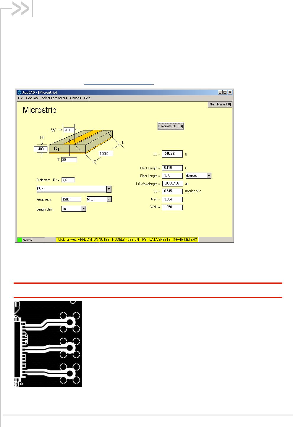
The RF signals must be routed using traces with a 50 characteristic impedance.
Basically, the characteristic impedance depends on the dielectric constant (εr) of the material used,
trace width (W), trace thickness (T), and height (H) between the trace and the reference ground plane.
In order to respect this constraint, Sierra Wireless recommends that a MicroStrip structure be used
and trace width be computed with a simulation tool (such as AppCAD, shown in the figure below and
available free of charge at http://www.avagotech.com).
Figure 1. AppCAD Screenshot for MicroStrip Design Power Mode Diagram
The trace width should be wide enough to maintain reasonable insertion loss and manufacturing
reliability. Cutting out inner layers of ground under the trace will increase the effective substrate
height; therefore, increasing the width of the RF trace.
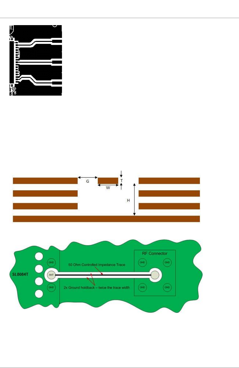
Caution: It is critical that no other signals (digital, analog, or supply) cross under the RF path. The figures
below show generic examples of good routing techniques.
Figure 2. RF Routing Example with Lead Type RF Connectors
4112719 Rev 2.1 January 07, 2013 15
Hardware Integration Guide
RF Circuit Routing Constraints
Figure 3. RF Routing Example with SMT Type RF Connectors
Fill the area around the RF traces with ground and ground vias to connect inner ground layers
for isolation.
Cut out ground fill under RF signal pads to reduce stray capacitance losses.
Avoid routing RF traces with sharp corners. A smooth radius is recommended.
The ground reference plane should be a solid continuous plane under the trace.
The coplanar clearance (G, below) from the trace to the ground should be at least the trace
width (W) and at least twice the height (H). This reduces the parasitic capacitance, which
potentially alters the trace impedance and increases the losses. Note the figure below shows
several internal ground layers cutout, which may not be necessary for every application.
Figure 4. Coplanar Clearance Example
Figure 5. Antenna Microstrip Routing Example
4112719 Rev 2.1 January 07, 2013 16
5. Audio Interface
The AirPrime SL8084T embedded module supports analog and PCM audio as summarized in the
following tables. Refer to document [2] AirPrime SL808x Product Technical Specification and
Customer Design Guidelines for detailed information about the audio interfaces.
Table 7. Audio Interface Features
Audio Type
Feature
Details
Analog
Implementation
Supports analog audio processing
Does not provide on-board filtering (except for blocking
capacitors on microphone lines)
Host must provide bias and signal filters
Host should terminate unused audio lines with pull-down
resistors
Digital (PCM)
Implementation
Primary PCM supported to interface with external codec
Power
1.8V (use VREG_MSME_1V8 as logic reference)
Table 8. Audio Pin Description
Audio Type
Signal Name
Pin #
Description
Notes
Analog
MIC_P
53
Microphone positive terminal
In series with 0.1 μF DC
blocking capacitor
MIC_N
54
Microphone negative terminal
In series with 0.1 μF DC
blocking capacitor
SPK_N
56
Speaker negative terminal
SPK_P
57
Speaker positive terminal
Digital
PCM_SYNC
64
PCM synchronization bit
8 kHz
PCM_DOUT
65
PCM output
PCM_DIN
66
PCM input
PCM_CLK
67
PCM clock
2 MHz for primary PCM mode
5.1. Audio Function Codec Responsibilities
The responsibilities of the module codec and host codec for special functions are detailed in the
following table.
Table 9. Codec Responsible for Special Functions
Function
Responsible
Codec
FIR filtering
Tx and Rx paths
Module
Noise suppression
Required due to high sensitivity and gain in Tx path
Module
Echo cancellation
Different for each audio path and environment (handset, headset,
car kit, speakerphone)
Module
High pass filtering/slope
filtering functions
Required per phone acoustic requirements
Module

4112719 Rev 2.1 January 07, 2013 17
Hardware Integration Guide
Audio Interface
Function
Responsible
Codec
AGC (Automatic Gain
Control)
Normalizes audio volumes in varying acoustic environments
Module
DTMF tones
Generation and detection of DTMF tones is required in both
directions of the phone Interface
Module
Comfort noise
Low level noise injected into Rx path for user ‘connection’
experience
Module
Simple ringers
Digital and analog tones, melody ringers, MIDI with limited
memory storage
Module
Voice memo
Performed by host if significant memory storage is required
Host
Polyphonic ringtones
Host often supports WAV, MIDI formats with significant memory
storage
Host
Path switching
Turn on audio path depending on user interface selection, or
headset detection
Host
Path mixing
Required for voice memo recording and playback via multiple
audio paths
Host
Transducer interfaces
Host provides acoustic drivers.
Must occur outside of path switching and mixing
Host
Adjustable gain/volume
settings
Based on user interface selections
Host/Module
DTMF/ringer tone
generation
Host/Module

4112719 Rev 2.1 January 07, 2013 18
6. Regulatory Information
6.1. Important Notice
Because of the nature of wireless communications, transmission and reception of data can never be
guaranteed. Data may be delayed, corrupted (i.e., have errors) or be totally lost. Although significant
delays or losses of data are rare when wireless devices such as the Sierra Wireless modem are used
in a normal manner with a well constructed network, the Sierra Wireless modem should not be used in
situations where failure to transmit or receive data could result in damage of any kind to the user or
any other party, including but not limited to personal injury, death, or loss of property. Sierra Wireless
and its affiliates accept no responsibility for damages of any kind resulting from delays or errors in
data transmitted or received using the Sierra Wireless modem, or for failure of the Sierra Wireless
modem to transmit or receive such data.
6.2. Safety and Hazards
Do not operate your AirPrime SL8084T modem:
In areas where blasting is in progress
Where explosive atmospheres may be present including refueling points, fuel depots, and
chemical plants
Near medical equipment, life support equipment, or any equipment which may be susceptible
to any form of radio interference. In such areas, the SL8084T modem MUST BE POWERED
OFF. Otherwise, the SL8084T modem can transmit signals that could interfere with this
equipment.
In an aircraft, the SL8084T modem MUST BE POWERED OFF. Otherwise, the SL8084T modem can
transmit signals that could interfere with various onboard systems and may be dangerous to the
operation of the aircraft or disrupt the cellular network. Use of a cellular phone in an aircraft is illegal in
some jurisdictions. Failure to observe this instruction may lead to suspension or denial of cellular
telephone services to the offender, or legal action or both.
Some airlines may permit the use of cellular phones while the aircraft is on the ground and the door is
open. The SL8084T modem may be used normally at this time.
6.3. Important Compliance Information for North
American Users
The SL8084T modem has been granted modular approval for mobile applications. Integrators may
use the SL8084T modem in their final products without additional FCC/IC (Industry Canada)
certification if they meet the following conditions. Otherwise, additional FCC/IC approvals must be
obtained.
1. At least 20 cm separation distance between the antenna and the user’s body must be
maintained at all times.
2. To comply with FCC/IC regulations limiting both maximum RF output power and human
exposure to RF radiation, the maximum antenna gain including cable loss in a mobile-only
exposure condition must not exceed 6 dBi in the cellular band and 3.5 dBi in the PCS band.
3. The SL8084T modem and its antenna must not be co-located or operating in conjunction with
any other transmitter or antenna within a host device.
4112719 Rev 2.1 January 07, 2013 19
Hardware Integration Guide
Regulatory Information
4. Refer to section 4 RF Circuit Routing Constraints for RF signal conditions.
5. A label must be affixed to the outside of the end product into which the SL8084T modem is
incorporated, with a statement similar to the following:
This device contains FCC ID: N7NSL8084T
This equipment contains equipment certified under IC: 2417C-SL8084T
6. A user manual with the end product must clearly indicate the operating requirements and
conditions that must be observed to ensure compliance with current FCC/IC RF exposure
guidelines.
The end product with an embedded SL8084T modem may also need to pass the FCC Part 15
unintentional emission testing requirements and be properly authorized per FCC Part 15.
Note: If this module is intended for use in a portable device, you are responsible for separate approval to
satisfy the SAR requirements of FCC Part 2.1093 and IC RSS-102.
6.3.1. EU Regulatory Conformity
Sierra Wireless hereby declares that the SL8084T modem conforms with all essential requirements of
Directive 1999/5/EC.
The Declaration of Conformity made under Directive 1999/5/EC is available for viewing at the
following location in the EU community:
Sierra Wireless (UK) Limited
Suite 5, The Hub
Fowler Avenue
Farnborough Business Park
Farnborough, United Kingdom GU14 7JP
4112719 Rev 2.1 January 07, 2013 20
7. References
7.1. Reference Documents
[1] Universal AirPrime SL Series Development Kit User Guide
Reference: WA_DEV_LG_UGD_003
[2] AirPrime SL808x Product Technical Specification and Customer Design Guidelines
Reference: 4111992
7.2. Acronyms and Definitions
Acronym or Term
Definition
AGC
Automatic Gain Control
BER
Bit Error Rate - a measure of receive sensitivity
BLER
Block Error Rate
Call Box
Base Station Simulator - Agilent E8285A or 8960, Rohde & Schwarz CMU200
CDMA
Code Division Multiple Access
dB
Decibel = 10 x log10 (P1/P2)
P1 is calculated power; P2 is reference power
Decibel = 20 x log10 (V1/V2)
V1 is calculated voltage, V2 is reference voltage
dBm
Decibels, relative to 1 mW - Decibel(mW) = 10 x log10 (Pwr (mW)/1mW)
DUT
Device Under Test
EDGE
Enhanced Data rates for GSM Evolution
EM
Embedded Module
ESD
ElectroStatic Discharge
FER
Frame Error Rate - a measure of receive sensitivity
GPRS
General Packet Radio Services
GPS
Global Positioning System
GSM
Global System for Mobile communications
Hz
Hertz = 1 cycle/second
inrush current
Peak current drawn when a device is connected or powered on
IS-2000
3G radio standards for voice and data (CDMA only)
IS-95
2G radio standards targeted for voice (cdmaONE)
LDO
Low Drop Out - refers to linear regulator
MHz
MegaHertz = 10E6 Hertz (Hertz = 1 cycle/second)
MIO
Module Input/Output
MPE
Maximum Permissible Exposure—the level of radiation to which a person may be
exposed without hazardous effect or adverse biological changes
OTA
Over-The-Air or Radiated through the antenna
PCS
Personal Communication System - PCS spans the 1.9 GHz radio spectrum

4112719 Rev 2.1 January 07, 2013 21
Hardware Integration Guide
References
Acronym or Term
Definition
RF
Radio Frequency
RMS
Root Mean Square
SA
Selective Availability
Sensitivity (Audio)
Measure of lowest power signal that the receiver can measure
Sensitivity (RF)
Measure of lowest power signal at the receiver input that can provide a prescribed
BER/BLER/SNR value at the receiver output.
SIM
Subscriber Identity Module
SL8084T
Sierra Wireless AirPrime soldered-down module used on GSM/UMTS networks
SNR
Signal to Noise Ratio
SOF
Start of Frame - a USB function
UART
Universal Asynchronous Receiver Transmitter
UMTS
Universal Mobile Telecommunications System
USB
Universal Serial Bus
USIM
Universal Subscriber Identity Module
VCC
Supply voltage
WCDMA
Wideband Code Division Multiple Access—In this document, the term “UMTS” is used
instead of “WCDMA”.
XIM
In this document, XIM is used as part of the contact identifiers for the USIM interface
(XIM_VCC, XIM_CLK, etc.).