Silex Technology PMACS Embedded wireless module User Manual silex technology Inc
Silex Technology, Inc. Embedded wireless module silex technology Inc
UserManual.wiki
>
Silex Technology
>
PMACS User Manual
Users Manual
Navigation menu
Upload a User Manual
Namespaces
Wiki Guide
HTML
PDF
Info
Views
User Manual
Discussion / Help
Navigation
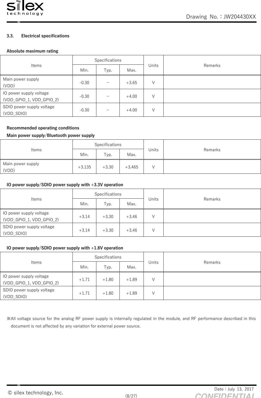
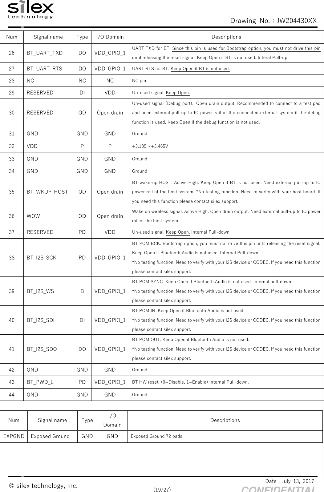
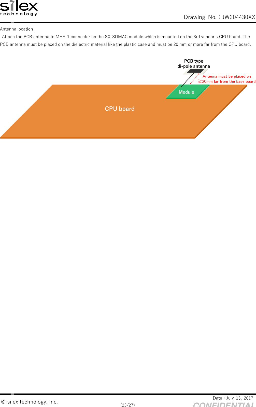
![Drawing No.:JW204430XX Date:July 13, 2017 (18/27) CONFIDENTIAL © silex technology, Inc. 4.2. Signal specifications Num Signal name Type I/O Domain Descriptions 1 GND GND GND Ground 2 NC NC NC NC pin 3 WLAN_PWD_L PD VDD_GPIO_1 WLAN reset. (0=Disable, 1=Enable) Internal Pull-down. 4 VDD P P +3.135~+3.465V 5 VDD P P +3.135~+3.465V 6 VDD P P +3.135~+3.465V 7 VDD P P +3.135~+3.465V 8 VDD_GPIO_1 P P +1.71 ~ +3.46V 9 VDD_GPIO_2 P P +1.71 ~ +3.46V 10 GND GND GND Ground 11 GND GND GND Ground 12 SD_D3 B VDD_SDIO SDIO Data[3] for WLAN. Since this pin is used for Bootstrap option, you must not drive this pin until releasing the reset signal. Internal Pull-up. 13 SD_D2 B VDD_SDIO SDIO Data[2] for WLAN. Since this pin is used for Bootstrap option, you must not drive this pin until releasing the reset signal. Interal Pull-up 14 SD_D1 B VDD_SDIO SDIO Data[1] for WLAN. Since this pin is used for Bootstrap option, you must not drive this pin until releasing the reset signal. Interal Pull-up 15 SD_D0 B VDD_SDIO SDIO Data[0] for WLAN. 16 SD_CMD B VDD_SDIO SDIO command for WLAN. 17 GND GND GND Ground 18 SD_CLK DI VDD_SDIO SDIO Clock for WLAN. 19 GND GND GND Ground 20 RESERVED DO VDD_SDIO Un-used signal. Keep Open. Since this pin is used for Bootstrap option, you must not drive this pin until releasing the reset signal. Internal Pull-up. 21 VDD_SDIO P P +1.71 ~ +3.46V 22 GND GND GND Ground 23 GND GND GND Ground 24 BT_UART_RXD DI VDD_GPIO_1 UART RXD for BT. Since this pin is used for Bootstrap option, you must not drive this pin until releasing the reset signal.Keep Open if BT is not used. Interal Pull-up. 25 BT_UART_CTS DI VDD_GPIO_1 UART CTS for BT. Since this pin is used for Bootstrap option, you must not drive this pin until releasing the reset signal. Keep Open if BT is not used. Interal Pull-up.](https://usermanual.wiki/Silex-Technology/PMACS/User-Guide-3510215-Page-18.png)