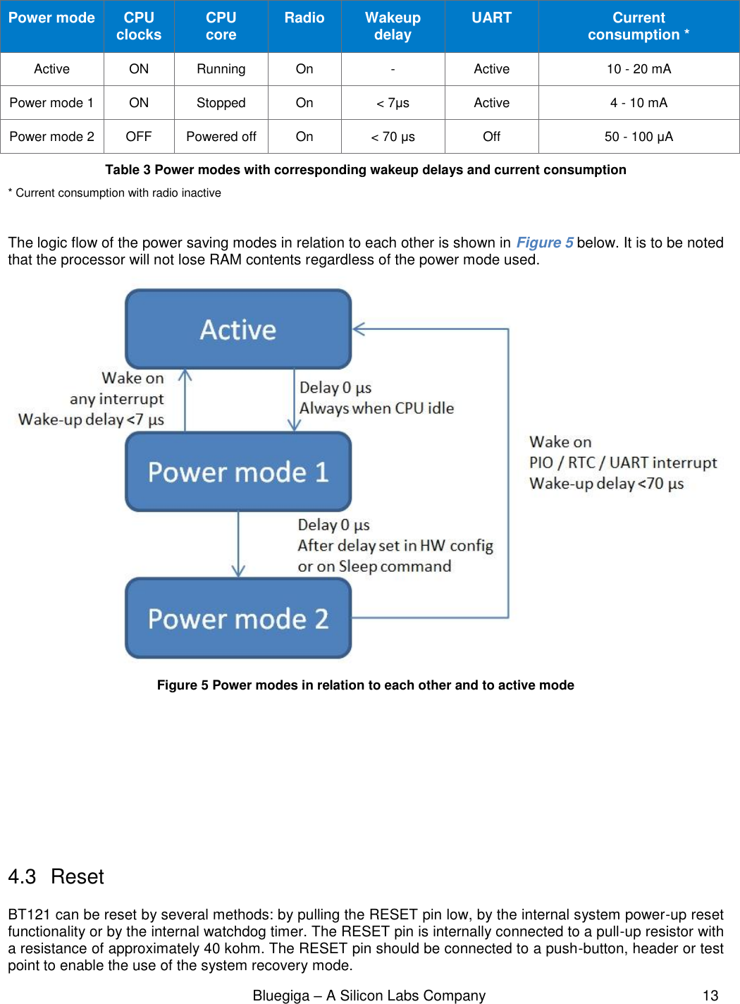
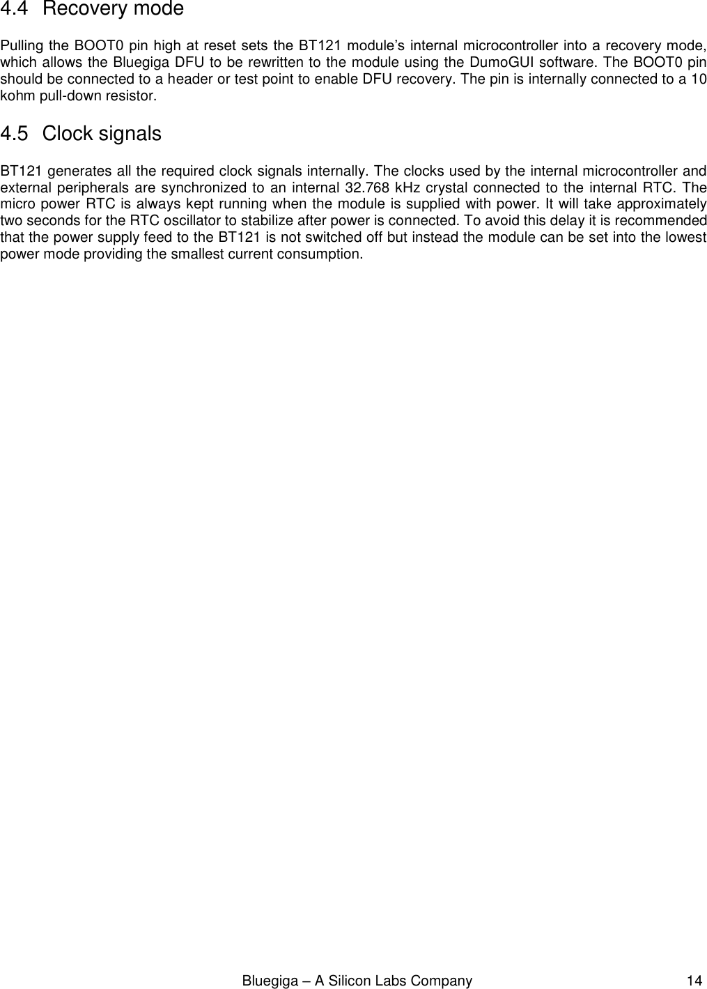
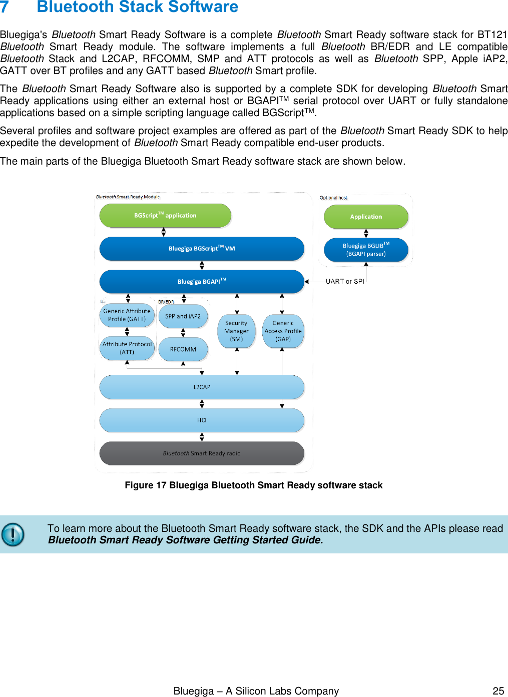
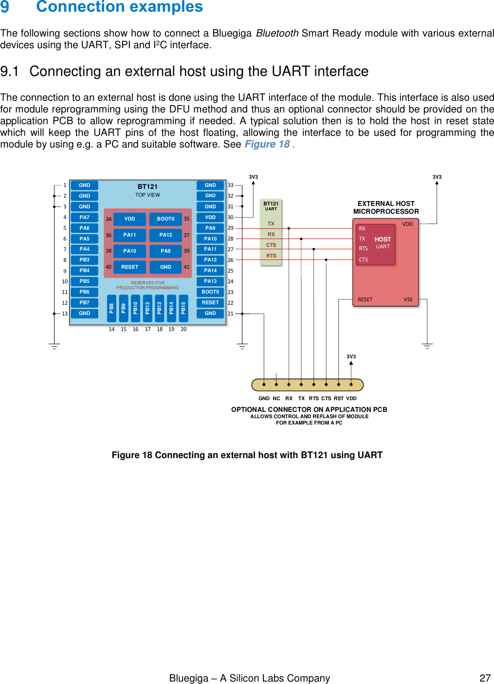
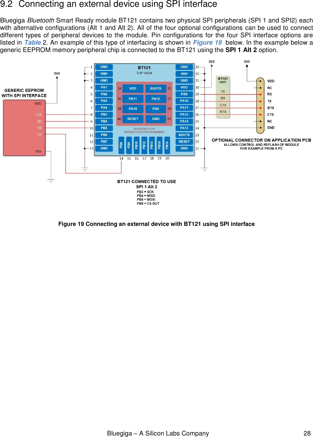
Silicon Laboratories Finland BT121 BT121 Bluetooth Smart Ready Module User Manual Product Data Sheet
Silicon Laboratories Finland Oy BT121 Bluetooth Smart Ready Module Product Data Sheet
UserManual.wiki
>
Silicon Laboratories Finland
>
BT121 User Manual
Datasheet
Navigation menu
Upload a User Manual
Namespaces
Wiki Guide
HTML
PDF
Info
Views
User Manual
Discussion / Help
Navigation
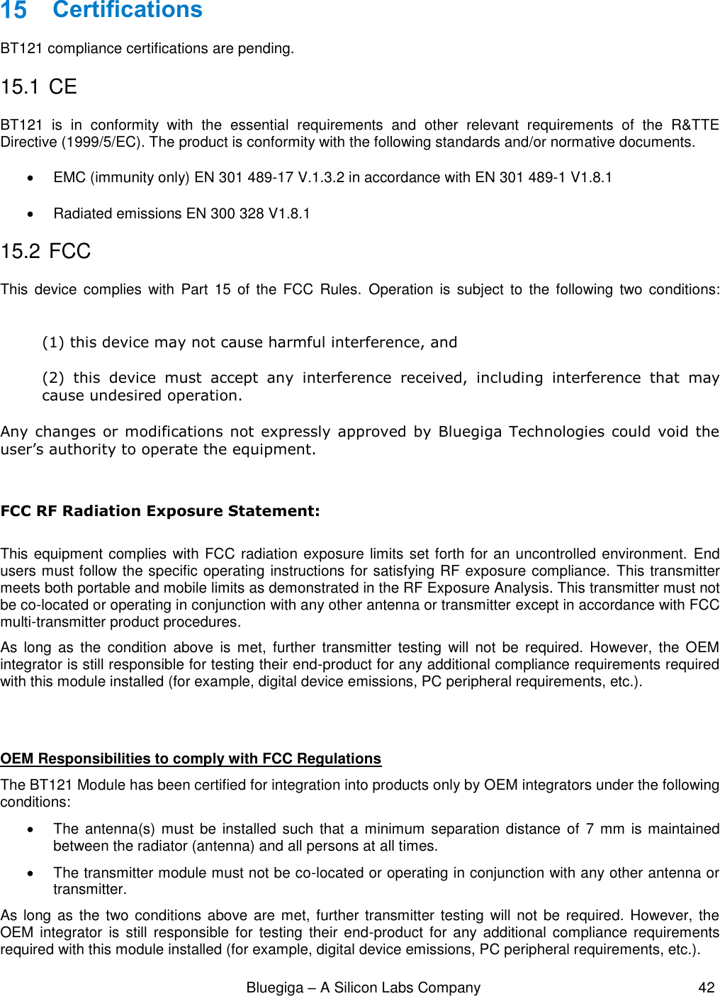
![Bluegiga – A Silicon Labs Company 40 Tape and reel packaging This section contains information regarding the tape and reel packaging and materials of packaging with dimensions for the Bluegiga Bluetooth Smart Ready BT121 module. 14.1 Reel material and dimensions Reel material PS Conductive Black – surface resistance 103 ↔ 105 Reel diameter 13” Reel color Black Table 19 Reel dimensions 14.2 Tape material and dimensions Tape material PS Conductive Black – surface resistance 103 ↔ 105 Table 20 Tape dimensions Symbol Dimensions [mm] D0 330.2 D1 100.0 W1 24.0 Symbol Dimensions [mm] P0 4.0 P1 16.0 D3 1.5 A0 11.3 B0 14.2 K0 2.7 W0 24.0 T 0.3](https://usermanual.wiki/Silicon-Laboratories-Finland/BT121/User-Guide-2649028-Page-40.png)
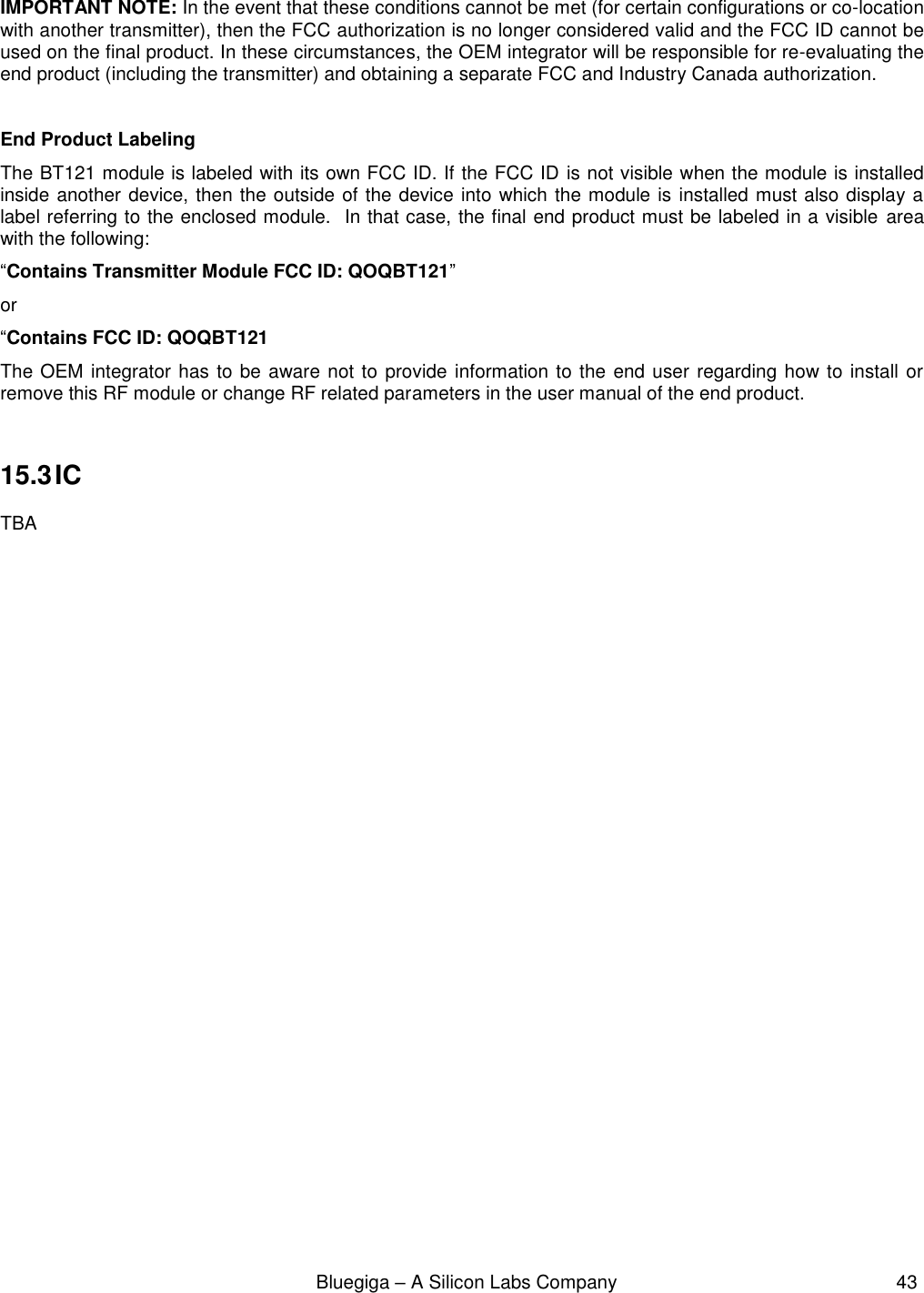
![Bluegiga – A Silicon Labs Company 41 14.3 Tape and reel box dimensions Table 21 Tape and reel box dimensions 14.4 Module orientation in tape Figure 25 Module orientation in tape and feed direction Symbol Dimensions [mm] W1 338 W2 344 W3 44](https://usermanual.wiki/Silicon-Laboratories-Finland/BT121/User-Guide-2649028-Page-41.png)