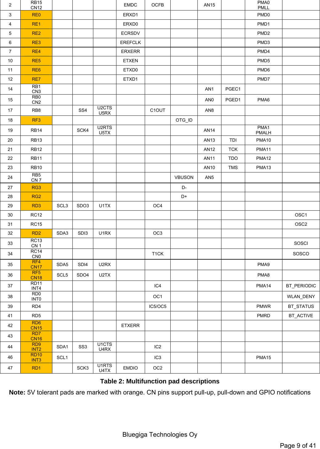
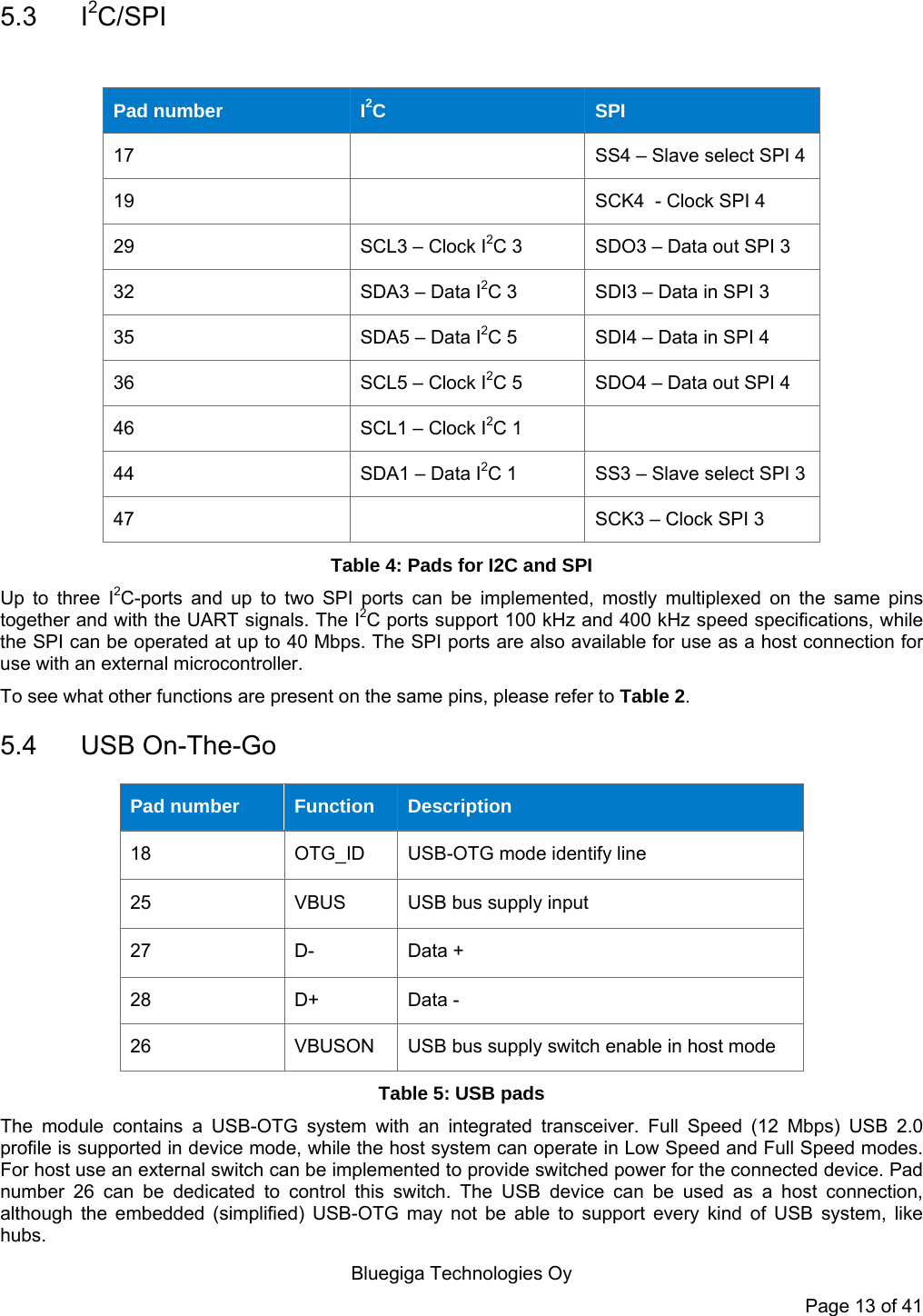
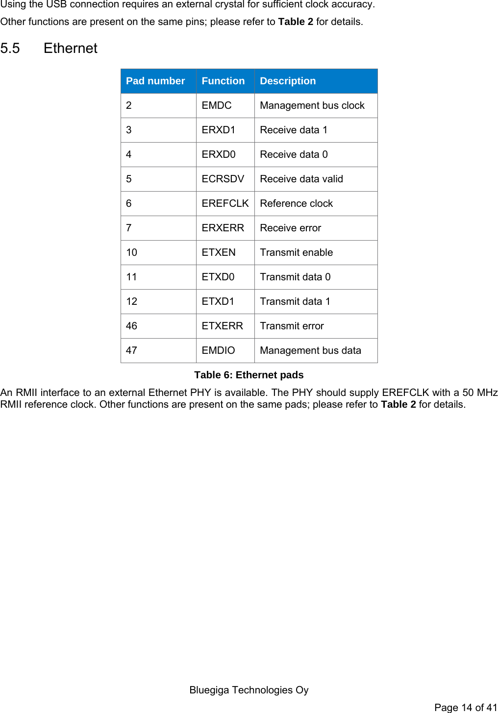
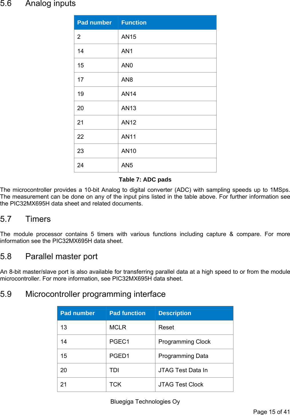
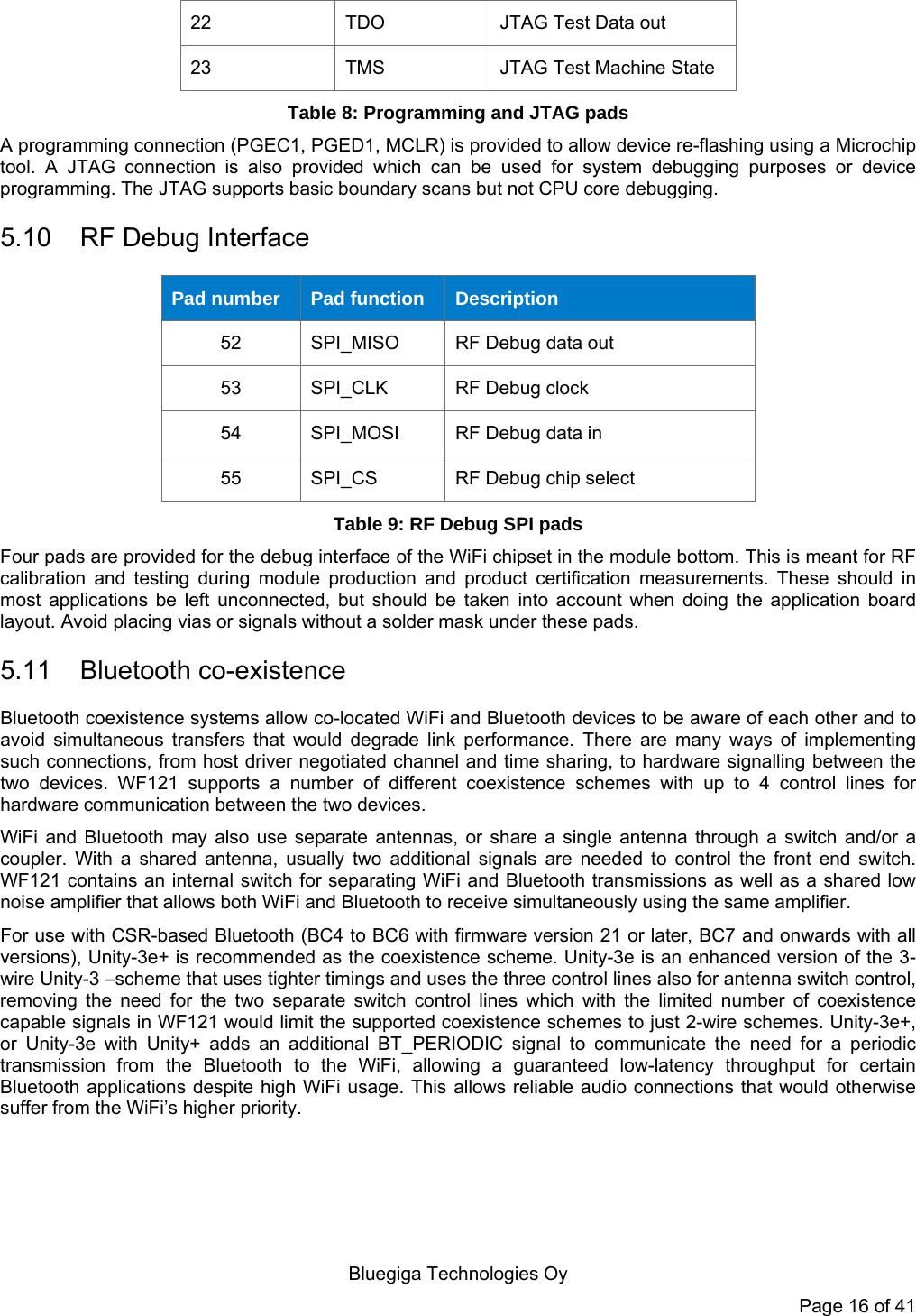
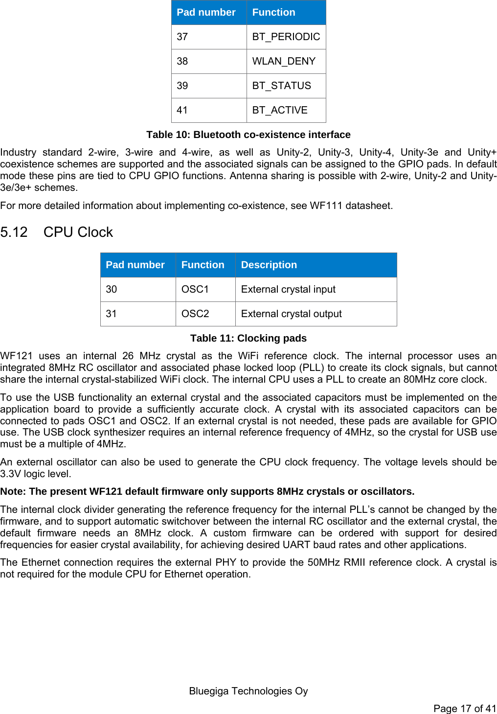
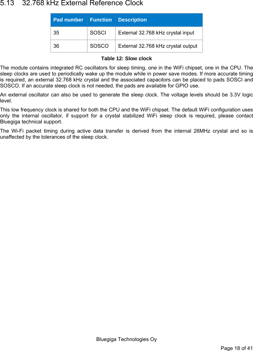
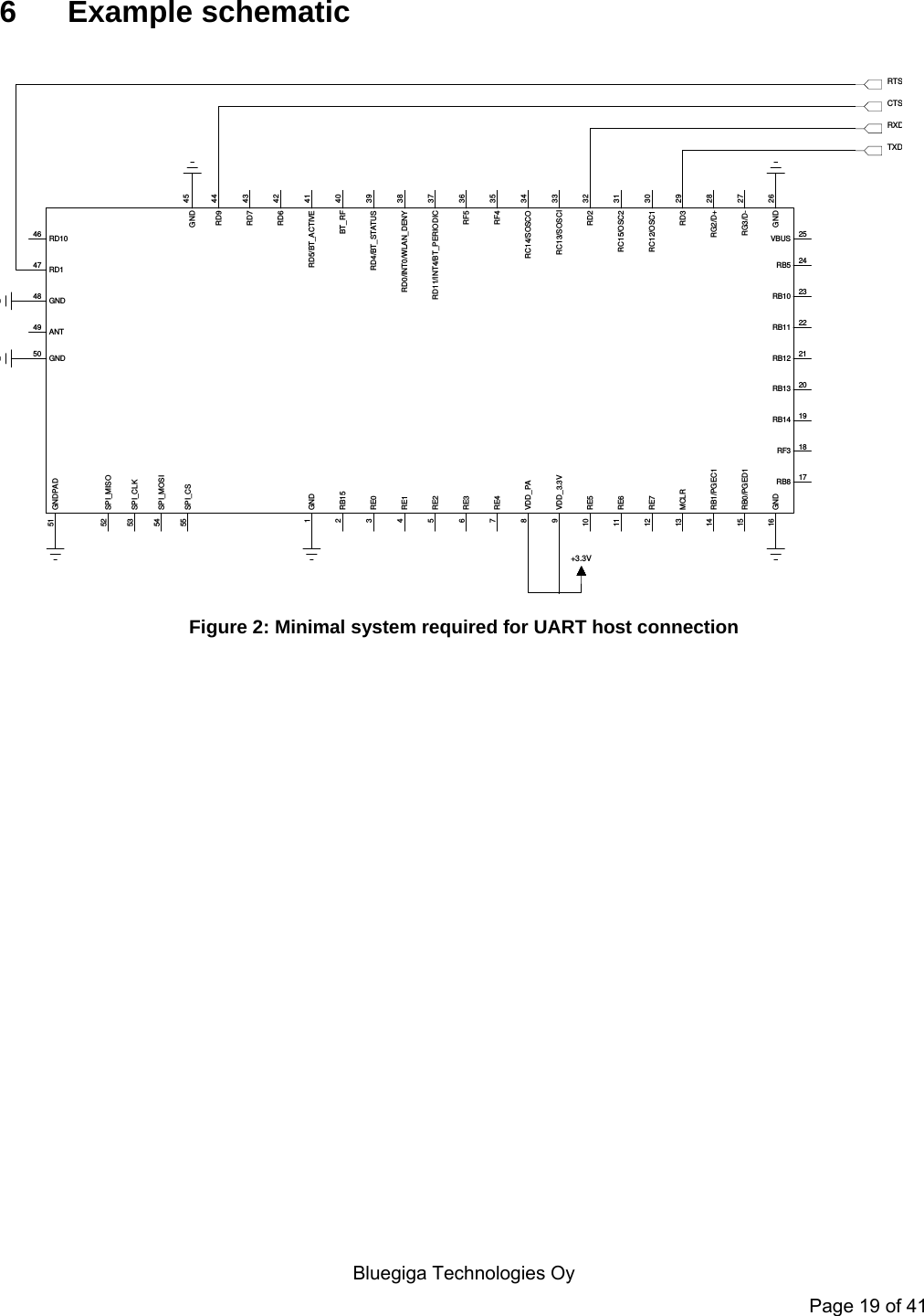
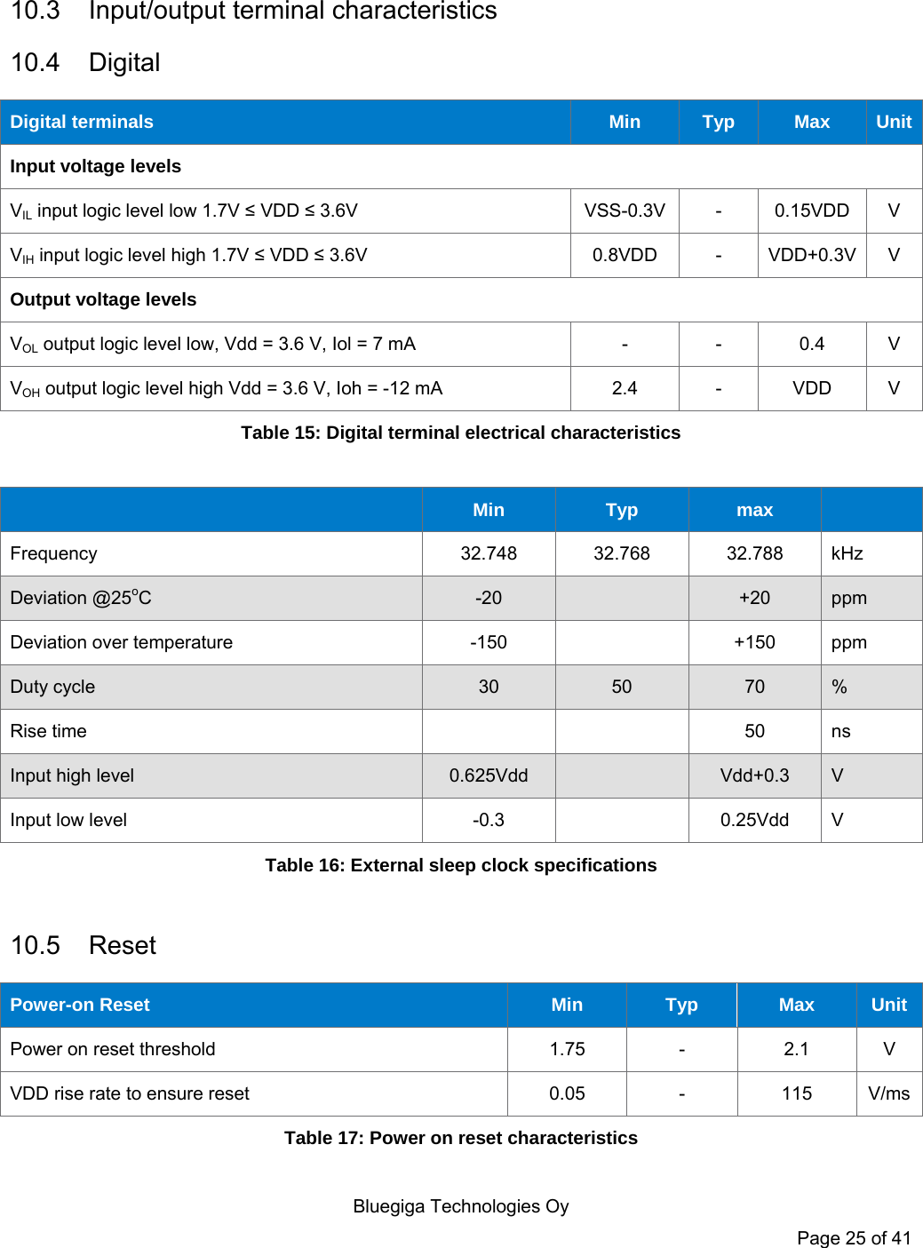
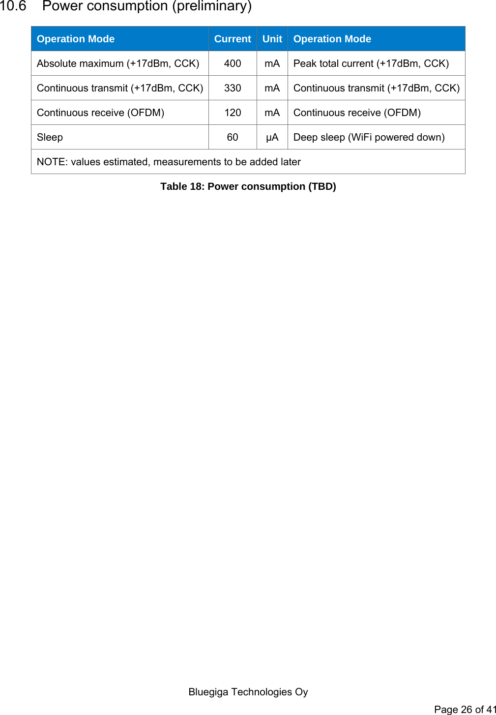
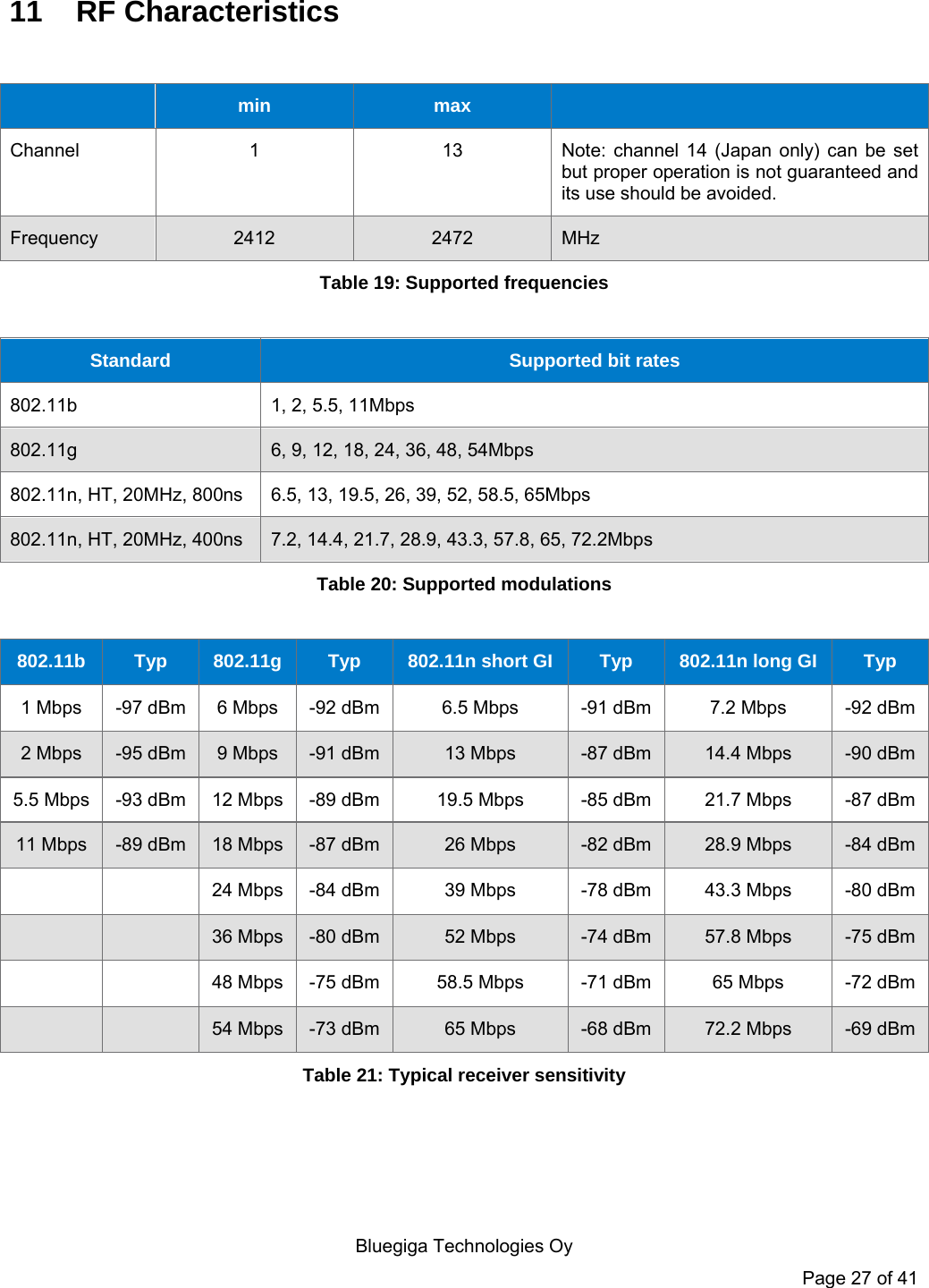
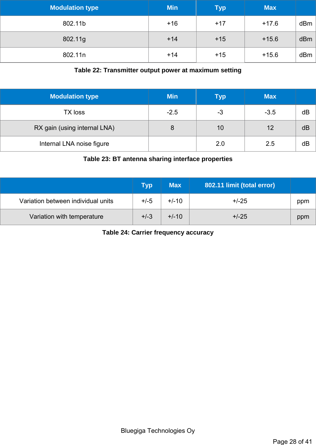
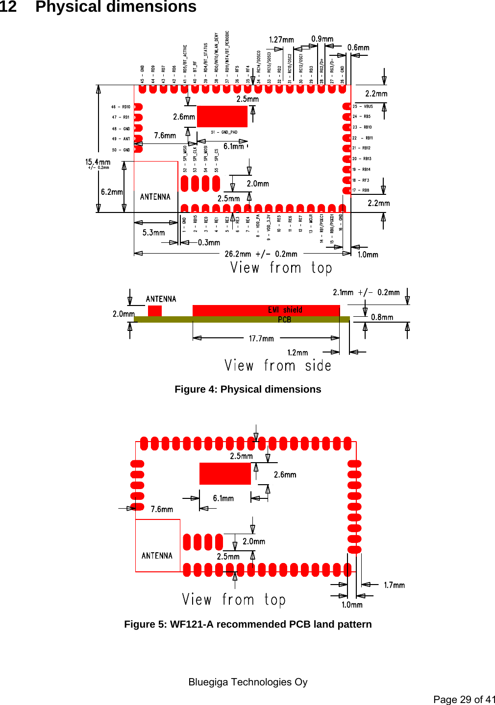
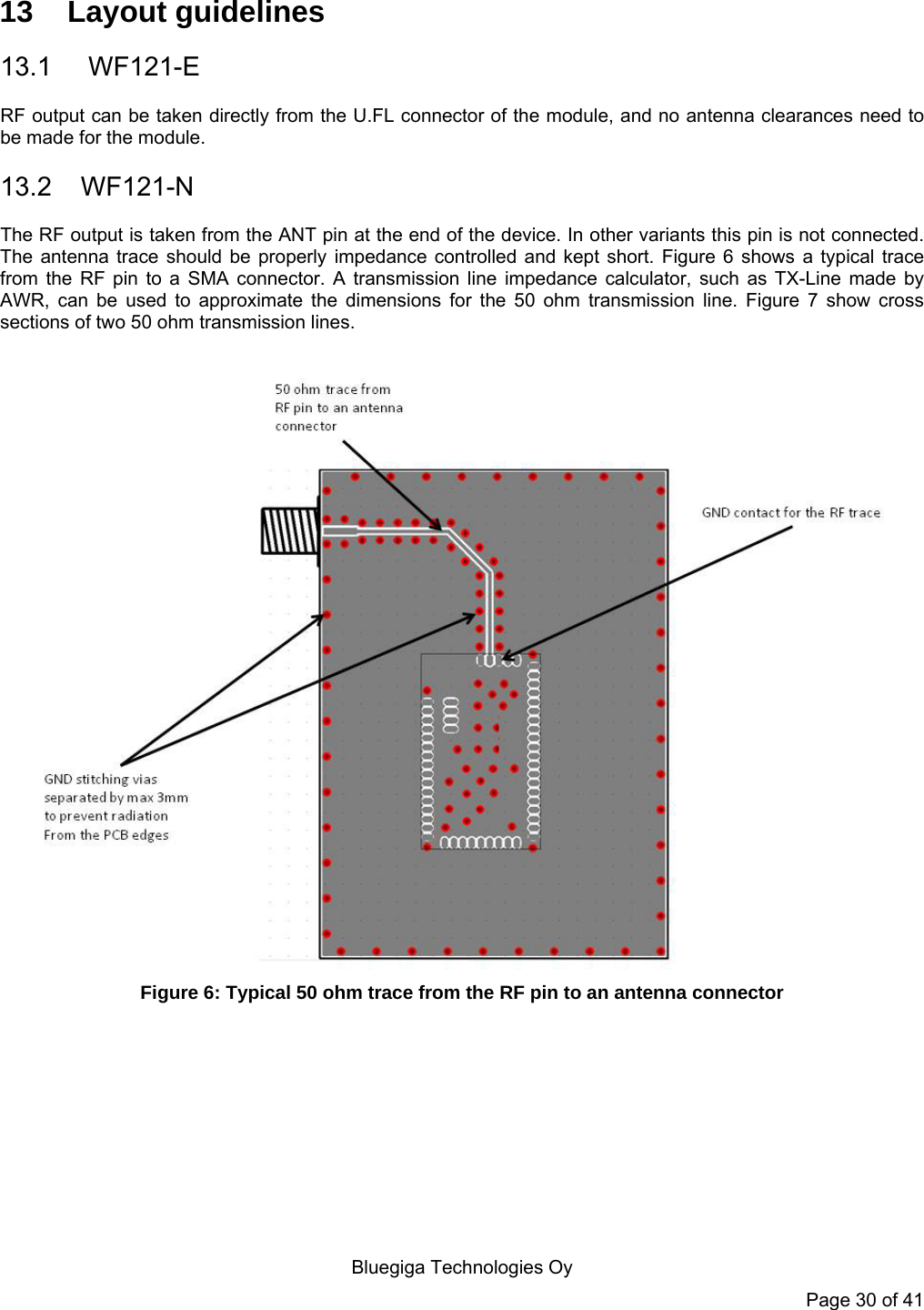
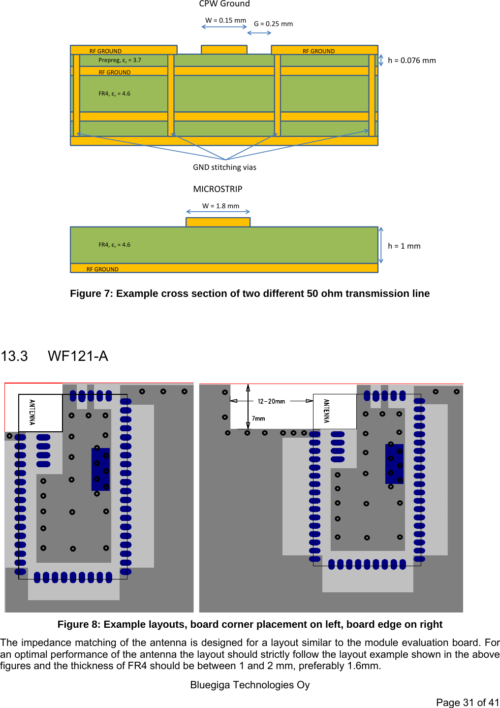
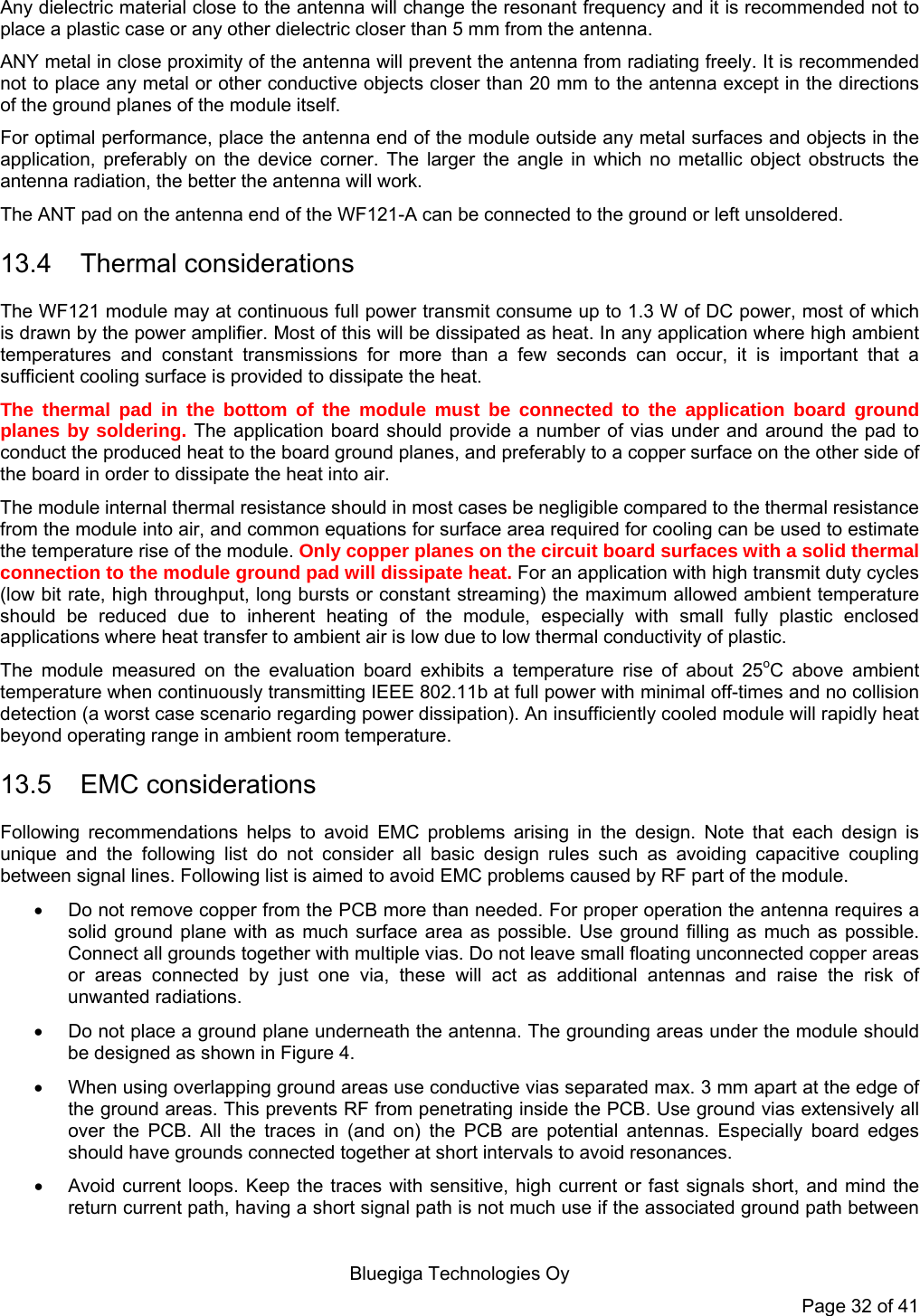
Silicon Laboratories Finland WF121 IEEE 802.11b/g/n Wi-Fi module WF121 User Manual WF121 v2 Datasheet

Silicon Laboratories Finland Oy IEEE 802.11b/g/n Wi-Fi module WF121 WF121 v2 Datasheet

Contents

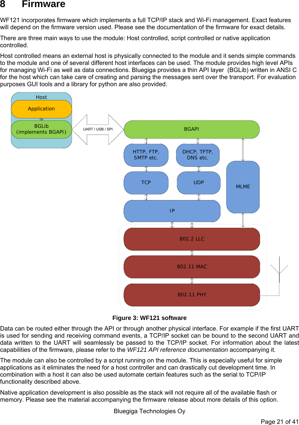
User Manual and Installation

                           WF121 Wi-Fi MODULE DATA SHEET Thursday, 12 July 2012 Version 1.2
  Bluegiga Technologies Oy                         Copyright © 2000-2012 Bluegiga Technologies All rights reserved.  Bluegiga Technologies assumes no responsibility for any errors which may appear in this manual.  Furthermore, Bluegiga Technologies reserves the right to alter the hardware, software, and/or specifications detailed here at any time without notice and does not make any commitment to update the information contained here. Bluegiga’s products are not authorized for use as critical components in life support devices or systems. The WRAP, Bluegiga Access Server, Access Point and iWRAP are registered trademarks of Bluegiga Technologies.  The Bluetooth trademark is owned by the Bluetooth SIG Inc., USA and is licensed to Bluegiga Technologies. All other trademarks listed herein are owned by their respective owners.
  Bluegiga Technologies Oy VERSION HISTORY Version  Comment 1.0   First version 1.1  FCC and IC information added 1.2  WF121-N layout guide
  Bluegiga Technologies Oy TABLE OF CONTENTS 1 Ordering Information..................................................................................................................................... 7 2 Pin-out and Terminal Descriptions ............................................................................................................... 8 3 Power control .............................................................................................................................................. 10 3.1 Power supply requirements ............................................................................................................... 10 3.2 Reset .................................................................................................................................................. 10 4 Microcontroller ............................................................................................................................................ 11 5 Interfaces .................................................................................................................................................... 12 5.1 General Purpose I/O pins .................................................................................................................. 12 5.2 Serial ports ......................................................................................................................................... 12 5.3 I2C/SPI ............................................................................................................................................... 13 5.4 USB On-The-Go ................................................................................................................................ 13 5.5 Ethernet ............................................................................................................................................. 14 5.6 Analog inputs ..................................................................................................................................... 15 5.7 Timers ................................................................................................................................................ 15 5.8 Parallel master port ............................................................................................................................ 15 5.9 Microcontroller programming interface .............................................................................................. 15 5.10 RF Debug Interface ........................................................................................................................... 16 5.11 Bluetooth co-existence ...................................................................................................................... 16 5.12 CPU Clock ......................................................................................................................................... 17 5.13 32.768 kHz External Reference Clock ............................................................................................... 18 6 Example schematic .................................................................................................................................... 19 7 802.11 Radio .............................................................................................................................................. 20 7.1 Wi-Fi Receiver ................................................................................................................................... 20 7.2 Wi-Fi Transmitter ............................................................................................................................... 20 7.3 Antenna switch for Bluetooth coexistence ......................................................................................... 20 8 Firmware ..................................................................................................................................................... 21 9 Host interfaces ............................................................................................................................................ 23 9.1 UART ................................................................................................................................................. 23 9.2 USB .................................................................................................................................................... 23 9.3 SPI ..................................................................................................................................................... 23 10 Electrical characteristics ........................................................................................................................ 24 10.1 Absolute maximum ratings ................................................................................................................ 24 10.2 Recommended operating conditions ................................................................................................. 24 10.3 Input/output terminal characteristics .................................................................................................. 25 10.4 Digital ................................................................................................................................................. 25 10.5 Reset .................................................................................................................................................. 25 10.6 Power consumption (preliminary) ...................................................................................................... 26
  Bluegiga Technologies Oy 11 RF Characteristics ................................................................................................................................. 27 12 Physical dimensions .............................................................................................................................. 29 13 Layout guidelines ................................................................................................................................... 30 13.1 WF121-E ............................................................................................................................................ 30 13.2 WF121-N ............................................................................................................................................ 30 13.3 WF121-A ............................................................................................................................................ 31 13.4 Thermal considerations ..................................................................................................................... 32 13.5 EMC considerations ........................................................................................................................... 32 14 Soldering recommendations .................................................................................................................. 34 15 Certifications .......................................................................................................................................... 35 15.1 CE ...................................................................................................................................................... 35 15.2 FCC and IC ........................................................................................................................................ 35 15.2.1 FCC et IC ................................................................................................................................... 37 16 Qualified Antenna Types for WF121-E .................................................................................................. 40 17 Contact information ................................................................................................................................ 41
  Bluegiga Technologies Oy DESCRIPTION WF121 is a self-contained Wi-Fi module providing a fully integrated 2.4GHz 802.11 b/g/n radio and a 32-bit microcontroller (MCU) platform, making it an ideal product for embedded applications requiring simple, low-cost and low-power wireless TCP/IP connectivity. WF121 also provides flexible interfaces for connecting to various peripherals.   WF121 allows end user applications to be embedded onto the on-board 32-bit microcontroller either using a simple BGScriptTM scripting language or for more sophisticated applications; ANSI C-language. This cuts out the need of an external MCU and allows the development of smaller and lower-cost products. However WF121 can also be used in modem-like mode in applications where the external MCU is needed.  With an integrated 802.11 radio, antenna, single power supply, and regulatory certifications, WF121 provides a low-risk and fast time-to-market for applications requiring Internet connectivity. This combined with Bluegiga’s excellent customer service will turn your Internet-of-Things applications into reality.  APPLICATIONS:  PoS terminals   RFID and laser scanners   Wi-Fi internet radios and audio streaming products  Wireless cameras   Video streaming    Portable navigation devices   Portable handheld devices   Wi-Fi medical sensors   Wireless picture frames KEY FEATURES:  2.4GHz band IEEE 802.11 b/g/n radio  Excellent radio performance:  TX power:   +17 dBm  RX sensitivity: -97 dBm  Host interfaces:  20Mbps UART   USB on-the-go  Peripheral interfaces:  GPIO, AIO and timers  I2C, SPI and UART  Ethernet  Embedded TCP/IP and 802.11 MAC stacks:  IP, TCP, UDP, DHCP and DNS protocols  BGAPI host protocol for modem like usage  BGScriptTM scripting language or native C-development for self-contained applications  32-bit embedded microcontroller  80Mhz, 128kB RAM and 512kB Flash  MIPS architecture  Temperature range: -40oC - +85oC  Fully CE, FCC and IC qualified  PHYSICAL OUTLOOK:   WF121-A
 Bluegiga Technologies Oy Page 7 of 41 1 Ordering Information Product code  Description WF121-A  WF121 module with integrated antenna WF121-E  WF121 module with U.FL connector  WF121-N WF121 module with RF pin. Non-standard product, so minimum order quantity applies.  Please contact: sales@bluegiga.com DKWF121  WF121 development kit
 Bluegiga Technologies Oy Page 8 of 41 2  Pin-out and Terminal Descriptions 24RB523RB1022RB1121RB1220RB1319RB1418RF317RB826GND27RG3/D-28RG2/D+29RD330RC12/OSC131RC15/OSC232RD233RC13/SOSCI34RC14/SOSCO35RF436RF537RD11/INT4/BT_PERIODIC38RD0/INT0/WLAN_DENY39RD4/BT_STATUS40BT_RF41RD5/BT_ACTIVE42RD616 GND15 RB0/PGED114 RB1/PGEC113 MCLR12 RE711 RE610 RE59VDD_3.3V8VDD_PA7RE46RE35RE24RE13RE02RB151GND44RD943RD745GND46 RD1047 RD148 GND49 ANT50 GND25VBUS51 GNDPAD52 SPI_MISO53 SPI_CLK54 SPI_MOSI55 SPI_CS Figure 1: WF121 pinout   Pad number  Function  Description 9  VDD_3.3V  Module power supply 8  VDD_PA  RF power amplifier power supply 1, 16, 26, 45, 48, 50  GND  Ground, connected together internally but should all be connected directly to a solid ground plane 51  GNDPAD  Thermal ground pad, should be soldered to a directly to a solid ground plane for improved thermal conductance 40  BT_RF  Bluetooth coexistence antenna connection, connect to ground through a 51ohm resistor if coexistence is not used 49  ANT  Antenna connection pad in N variant of the module, in other variants not connected 25  VBUS  USB VBUS input 13  MCLR Module reset, also used for programming using a Microchip tool. Internal pull-up, can be left floating or connected to ground through a 100nF capacitor for delayed power-up reset (note: Microchip ICSP programming tools will not work with a capacitor) Table 1: Single function pad descriptions    PAD#  GPIO  I2C  SPI  UART  Ethernet  Timer  USB  Analog  Prog.  Parallel  Other
 Bluegiga Technologies Oy Page 9 of 41 2  RB15 CN12     EMDC OCFB   AN15   PMA0 PMLL   3  RE0    ERXD1 PMD0  4  RE1    ERXD0 PMD1  5  RE2    ECRSDV PMD2  6  RE3    EREFCLK PMD3  7  RE4    ERXERR PMD4  10  RE5    ETXEN PMD5  11  RE6    ETXD0 PMD6  12  RE7    ETXD1 PMD7  14  RB1 CN3          AN1 PGEC1    15  RB0 CN2          AN0 PGED1  PMA6   17 RB8   SS4  U2CTS U5RX  C1OUT   AN8      18  RF3        OTG_ID        19 RB14   SCK4  U2RTS U5TX      AN14   PMA1 PMALH   20 RB13     AN13 TDI  PMA10   21 RB12     AN12 TCK  PMA11   22 RB11     AN11 TDO  PMA12   23 RB10     AN10 TMS  PMA13   24  RB5 CN 7            VBUSON AN5      27  RG3     D-    28  RG2     D+    29  RD3 SCL3 SDO3 U1TX  OC4    30 RC12      OSC1 31 RC15      OSC2 32  RD2 SDA3 SDI3 U1RX  OC3    33  RC13 CN 1                    SOSCI 34  RC14 CN0      T1CK        SOSCO 35  RF4 CN17  SDA5 SDI4  U2RX       PMA9  36  RF5 CN18  SCL5 SDO4  U2TX       PMA8  37  RD11 INT4        IC4     PMA14 BT_PERIODIC 38  RD0 INT0        OC1       WLAN_DENY 39 RD4     IC5/OC5 PMWR BT_STATUS 41 RD5     PMRD BT_ACTIVE 42  RD6 CN15     ETXERR          43  RD7 CN16                    44  RD9 INT2  SDA1 SS3 U1CTS U4RX   IC2         46  RD10 INT3  SCL1       IC3        PMA15   47  RD1  SCK3 U1RTS U4TX  EMDIO OC2           Table 2: Multifunction pad descriptions Note: 5V tolerant pads are marked with orange. CN pins support pull-up, pull-down and GPIO notifications
 Bluegiga Technologies Oy Page 10 of 41 3 Power control 3.1  Power supply requirements WF121 is designed to operate with a 3.3V nominal input voltage supplied to two module pads. The VDD_3.3V pad can be fed with a voltage between 2.3V and 3.6V and is used to power the internal microcontroller. The VDD_PA pad can be supplied with a voltage between 2.7V and 4.8V and supplies the RF power amplifier and the internal switch-mode converter powering the WiFi digital core.  In lithium battery powered applications, VDD_PA can be connected directly to the battery, while a regulator is needed to supply the VDD_3.3V with a lower voltage, as needed by the design. The VDD_PA supply should be capable of providing at least 350mA, though the average consumption of the module will be much less than that. The VDD_3.3V supply will draw a peak current of less than 100mA, not including current drawn from the GPIO pins. The PA supply should preferably be bypassed with a 10 to 100µF capacitor to smooth out the current spikes drawn by the Wi-Fi power amplifier. External high frequency bypassing is not needed, the module contains the needed supply filtering capacitors. While the Wi-Fi power saving modes reduce the idle consumption to very low levels, it may in some applications be useful to reduce the consumption even further. For this purpose, the Wi-Fi part of the module can be fully shut down internally by disabling the internal switch mode converter to minimize power consumption, though restarting it requires a new WiFi core power-up initialization. This will usually take several seconds, but in applications where a connection is required only once a few minutes or this might not be an issue while the reduced consumption can be very valuable. The WF121 module automatically applies various power saving modes during operation to minimize average power consumption. 3.2 Reset WF121 can be reset by the MCLR-pin (active low), system power up, the internal brown-out detector or the internal watchdog timer.
 Bluegiga Technologies Oy Page 11 of 41 4 Microcontroller WF121 contains a Microchip PIC32-series microcontroller with a MIPS M4K core. At a maximum clock frequency of 80 MHz the core can reach a performance of 125 DMIPS while keeping low power consumption. The microcontroller used in WF121 contains 512kB of Flash memory and 128kB of SRAM.  Most peripheral features are directly provided by the microcontroller and for low level information and detailed descriptions please refer to the material and datasheets of the PIC32MX695H.
 Bluegiga Technologies Oy Page 12 of 41 5 Interfaces 5.1  General Purpose I/O pins To see which GPIOs are multiplexed with which features, please refer to Table 2. .WF121 contains a number of pads that can be configured to be used as general purpose digital IO’s, analog inputs or for various built-in functions. Provided functions include a Full Speed USB-OTG port, three I2C-ports, two SPI-ports, two to four UART’s, Ethernet MAC with RMII connection and various timer functions. Some of the pads are 5V tolerant. All GPIO pads can drive currents of up to +/- 25 mA. Four pins are available for implementing a coexistence scheme with a Bluetooth device. The exact order and function as well as the coexistence system desired is software configurable, with the default pad bindings shown in Table 3 for a Unity-3e+ coexistence scheme. If the pads are bound to WiFi chip pins, the CPU pins associated with the pads must be set to inputs. 5.2 Serial ports Pad number  UART 1  UART 2  UART 4  UART 5 17   CTS   RX 21   RTS   TX 29  TX     32  RX     35   RX     36   TX     44  CTS   RX   47  RTS   TX   Table 3: Serial port pads Two UART’s are provided with RTS/CTS-handshaking. If handshaking is not needed, up to four UART’s can be implemented. Speeds up to 20 Mbps are possible, but the higher bit rates might require the use of an external crystal for sufficient clock accuracy. The serial ports can also be used as host connections when using an external microcontroller. To see what other functions are present on the same pins, please refer to Table 2.  .
 Bluegiga Technologies Oy Page 13 of 41 5.3 I2C/SPI  Pad number  I2C  SPI 17   SS4 – Slave select SPI 4 19   SCK4  - Clock SPI 4 29  SCL3 – Clock I2C 3  SDO3 – Data out SPI 3 32  SDA3 – Data I2C 3  SDI3 – Data in SPI 3 35  SDA5 – Data I2C 5  SDI4 – Data in SPI 4 36  SCL5 – Clock I2C 5   SDO4 – Data out SPI 4 46  SCL1 – Clock I2C 1   44  SDA1 – Data I2C 1  SS3 – Slave select SPI 3 47   SCK3 – Clock SPI 3 Table 4: Pads for I2C and SPI Up to three I2C-ports and up to two SPI ports can be implemented, mostly multiplexed on the same pins together and with the UART signals. The I2C ports support 100 kHz and 400 kHz speed specifications, while the SPI can be operated at up to 40 Mbps. The SPI ports are also available for use as a host connection for use with an external microcontroller. To see what other functions are present on the same pins, please refer to Table 2. 5.4 USB On-The-Go Pad number  Function  Description 18  OTG_ID  USB-OTG mode identify line 25  VBUS  USB bus supply input 27  D-  Data + 28  D+  Data - 26  VBUSON  USB bus supply switch enable in host mode Table 5: USB pads The module contains a USB-OTG system with an integrated transceiver. Full Speed (12 Mbps) USB 2.0 profile is supported in device mode, while the host system can operate in Low Speed and Full Speed modes. For host use an external switch can be implemented to provide switched power for the connected device. Pad number 26 can be dedicated to control this switch. The USB device can be used as a host connection, although the embedded (simplified) USB-OTG may not be able to support every kind of USB system, like hubs.
 Bluegiga Technologies Oy Page 14 of 41 Using the USB connection requires an external crystal for sufficient clock accuracy. Other functions are present on the same pins; please refer to Table 2 for details. 5.5 Ethernet Pad number  Function  Description 2  EMDC  Management bus clock 3  ERXD1  Receive data 1 4  ERXD0  Receive data 0 5  ECRSDV  Receive data valid 6  EREFCLK Reference clock 7  ERXERR  Receive error 10  ETXEN  Transmit enable 11  ETXD0  Transmit data 0 12  ETXD1  Transmit data 1 46  ETXERR  Transmit error 47  EMDIO  Management bus data Table 6: Ethernet pads An RMII interface to an external Ethernet PHY is available. The PHY should supply EREFCLK with a 50 MHz RMII reference clock. Other functions are present on the same pads; please refer to Table 2 for details.
 Bluegiga Technologies Oy Page 15 of 41 5.6 Analog inputs Pad number  Function 2  AN15 14  AN1 15  AN0 17  AN8 19  AN14 20  AN13 21  AN12 22  AN11 23  AN10 24  AN5 Table 7: ADC pads The microcontroller provides a 10-bit Analog to digital converter (ADC) with sampling speeds up to 1MSps. The measurement can be done on any of the input pins listed in the table above. For further information see the PIC32MX695H data sheet and related documents. 5.7 Timers The module processor contains 5 timers with various functions including capture & compare. For more information see the PIC32MX695H data sheet. 5.8 Parallel master port An 8-bit master/slave port is also available for transferring parallel data at a high speed to or from the module microcontroller. For more information, see PIC32MX695H data sheet. 5.9  Microcontroller programming interface Pad number  Pad function  Description 13  MCLR  Reset 14  PGEC1  Programming Clock 15  PGED1  Programming Data 20  TDI  JTAG Test Data In 21  TCK  JTAG Test Clock
 Bluegiga Technologies Oy Page 16 of 41 22  TDO  JTAG Test Data out 23  TMS  JTAG Test Machine State Table 8: Programming and JTAG pads A programming connection (PGEC1, PGED1, MCLR) is provided to allow device re-flashing using a Microchip tool. A JTAG connection is also provided which can be used for system debugging purposes or device programming. The JTAG supports basic boundary scans but not CPU core debugging. 5.10  RF Debug Interface Pad number  Pad function  Description 52  SPI_MISO  RF Debug data out 53  SPI_CLK  RF Debug clock 54  SPI_MOSI  RF Debug data in 55  SPI_CS  RF Debug chip select Table 9: RF Debug SPI pads Four pads are provided for the debug interface of the WiFi chipset in the module bottom. This is meant for RF calibration and testing during module production and product certification measurements. These should in most applications be left unconnected, but should be taken into account when doing the application board layout. Avoid placing vias or signals without a solder mask under these pads.  5.11 Bluetooth co-existence Bluetooth coexistence systems allow co-located WiFi and Bluetooth devices to be aware of each other and to avoid simultaneous transfers that would degrade link performance. There are many ways of implementing such connections, from host driver negotiated channel and time sharing, to hardware signalling between the two devices. WF121 supports a number of different coexistence schemes with up to 4 control lines for hardware communication between the two devices. WiFi and Bluetooth may also use separate antennas, or share a single antenna through a switch and/or a coupler. With a shared antenna, usually two additional signals are needed to control the front end switch. WF121 contains an internal switch for separating WiFi and Bluetooth transmissions as well as a shared low noise amplifier that allows both WiFi and Bluetooth to receive simultaneously using the same amplifier.  For use with CSR-based Bluetooth (BC4 to BC6 with firmware version 21 or later, BC7 and onwards with all versions), Unity-3e+ is recommended as the coexistence scheme. Unity-3e is an enhanced version of the 3-wire Unity-3 –scheme that uses tighter timings and uses the three control lines also for antenna switch control, removing the need for the two separate switch control lines which with the limited number of coexistence capable signals in WF121 would limit the supported coexistence schemes to just 2-wire schemes. Unity-3e+, or Unity-3e with Unity+ adds an additional BT_PERIODIC signal to communicate the need for a periodic transmission from the Bluetooth to the WiFi, allowing a guaranteed low-latency throughput for certain Bluetooth applications despite high WiFi usage. This allows reliable audio connections that would otherwise suffer from the WiFi’s higher priority.
 Bluegiga Technologies Oy Page 17 of 41 Pad number  Function 37  BT_PERIODIC38  WLAN_DENY 39  BT_STATUS 41  BT_ACTIVE Table 10: Bluetooth co-existence interface Industry standard 2-wire, 3-wire and 4-wire, as well as Unity-2, Unity-3, Unity-4, Unity-3e and Unity+ coexistence schemes are supported and the associated signals can be assigned to the GPIO pads. In default mode these pins are tied to CPU GPIO functions. Antenna sharing is possible with 2-wire, Unity-2 and Unity-3e/3e+ schemes. For more detailed information about implementing co-existence, see WF111 datasheet. 5.12 CPU Clock Pad number  Function  Description 30  OSC1  External crystal input 31  OSC2  External crystal output Table 11: Clocking pads WF121 uses an internal 26 MHz crystal as the WiFi reference clock. The internal processor uses an integrated 8MHz RC oscillator and associated phase locked loop (PLL) to create its clock signals, but cannot share the internal crystal-stabilized WiFi clock. The internal CPU uses a PLL to create an 80MHz core clock. To use the USB functionality an external crystal and the associated capacitors must be implemented on the application board to provide a sufficiently accurate clock. A crystal with its associated capacitors can be connected to pads OSC1 and OSC2. If an external crystal is not needed, these pads are available for GPIO use. The USB clock synthesizer requires an internal reference frequency of 4MHz, so the crystal for USB use must be a multiple of 4MHz. An external oscillator can also be used to generate the CPU clock frequency. The voltage levels should be 3.3V logic level. Note: The present WF121 default firmware only supports 8MHz crystals or oscillators. The internal clock divider generating the reference frequency for the internal PLL’s cannot be changed by the firmware, and to support automatic switchover between the internal RC oscillator and the external crystal, the default firmware needs an 8MHz clock. A custom firmware can be ordered with support for desired frequencies for easier crystal availability, for achieving desired UART baud rates and other applications. The Ethernet connection requires the external PHY to provide the 50MHz RMII reference clock. A crystal is not required for the module CPU for Ethernet operation.
 Bluegiga Technologies Oy Page 18 of 41  5.13  32.768 kHz External Reference Clock Pad number  Function  Description 35  SOSCI  External 32.768 kHz crystal input 36  SOSCO  External 32.768 kHz crystal output Table 12: Slow clock The module contains integrated RC oscillators for sleep timing, one in the WiFi chipset, one in the CPU. The sleep clocks are used to periodically wake up the module while in power save modes. If more accurate timing is required, an external 32.768 kHz crystal and the associated capacitors can be placed to pads SOSCI and SOSCO. If an accurate sleep clock is not needed, the pads are available for GPIO use.  An external oscillator can also be used to generate the sleep clock. The voltage levels should be 3.3V logic level. This low frequency clock is shared for both the CPU and the WiFi chipset. The default WiFi configuration uses only the internal oscillator, if support for a crystal stabilized WiFi sleep clock is required, please contact Bluegiga technical support. The Wi-Fi packet timing during active data transfer is derived from the internal 26MHz crystal and so is unaffected by the tolerances of the sleep clock.
 Bluegiga Technologies Oy Page 19 of 41 6 Example schematic 24RB523RB1022RB1121RB1220RB1319RB1418RF317RB826GND27RG3/D-28RG2/D+29RD330RC12/OSC131RC15/OSC232RD233RC13/SOSCI34RC14/SOSCO35RF436RF537RD11/INT4/BT_PERIODIC38RD0/INT0/WLAN_DENY39RD4/BT_STATUS40BT_RF41RD5/BT_ACTIVE42RD616 GND15 RB0/PGED114 RB1/PGEC113 MCLR12 RE711 RE610 RE59VDD_3.3V8VDD_PA7RE46RE35RE24RE13RE02RB151GND44RD943RD745GND46 RD1047 RD148 GND49 ANT50 GND25VBUS51 GNDPAD52 SPI_MISO53 SPI_CLK54 SPI_MOSI55 SPI_CS+3.3VTXDRXDCTSRTS Figure 2: Minimal system required for UART host connection
 Bluegiga Technologies Oy Page 20 of 41 7 802.11 Radio 7.1 Wi-Fi Receiver The receiver features direct conversion architecture. Sufficient out-of-band blocking specification at the Low Noise Amplifier (LNA) input allows the receiver to be used in close proximity to GSM and WCDMA cellular phone transmitters without being desensitized. High-order baseband filters ensure good performance against in-band interference. 7.2 Wi-Fi Transmitter The transmitter features a direct IQ modulator. Digital baseband transmit circuitry provides the required spectral shaping and on-chip trims are used to reduce IQ modulator distortion. Transmitter gain can be controlled on a per-packet basis, allowing the optimization of the transmit power as a function of modulation scheme. The internal Power Amplifier (PA) has a maximum output power of +15dBm for IEEE 802.11g/n and +17dBm for IEEE 802.11b. The module internally compensates for PA gain and reference oscillator frequency drifts with varying temperature and supply voltage. 7.3 Antenna switch for Bluetooth coexistence WF121 supports sharing the integrated antenna or antenna connector with a Bluetooth device through the BT_RF pad. The module contains a bypass switch to route the Bluetooth signal directly to the antenna, and supports using the internal LNA for Bluetooth reception. The switch is controlled through the coexistence interface.
 Bluegiga Technologies Oy Page 21 of 41 8 Firmware WF121 incorporates firmware which implements a full TCP/IP stack and Wi-Fi management. Exact features will depend on the firmware version used. Please see the documentation of the firmware for exact details. There are three main ways to use the module: Host controlled, script controlled or native application controlled. Host controlled means an external host is physically connected to the module and it sends simple commands to the module and one of several different host interfaces can be used. The module provides high level APIs for managing Wi-Fi as well as data connections. Bluegiga provides a thin API layer  (BGLib) written in ANSI C for the host which can take care of creating and parsing the messages sent over the transport. For evaluation purposes GUI tools and a library for python are also provided. IPBGAPI802.2 LLC802.11 MACUART / USB / SPIHostUDPTCPBGLib (implements BGAPI)ApplicationMLME802.11 PHYHTTP, FTP, SMTP etc. DHCP, TFTP, DNS etc. Figure 3: WF121 software Data can be routed either through the API or through another physical interface. For example if the first UART is used for sending and receiving command events, a TCP/IP socket can be bound to the second UART and data written to the UART will seamlessly be passed to the TCP/IP socket. For information about the latest capabilities of the firmware, please refer to the WF121 API reference documentation accompanying it. The module can also be controlled by a script running on the module. This is especially useful for simple applications as it eliminates the need for a host controller and can drastically cut development time. In combination with a host it can also be used automate certain features such as the serial to TCP/IP functionality described above. Native application development is also possible as the stack will not require all of the available flash or memory. Please see the material accompanying the firmware release about more details of this option.
 Bluegiga Technologies Oy Page 22 of 41
 Bluegiga Technologies Oy Page 23 of 41 9 Host interfaces 9.1 UART The module can be controlled over the UART interface. In order for the communication to be reliable, hardware flow control signals (RTS and CTS) must be present between the host and the module. When using high UART transfer speeds (between 1 and 20Mbps) an external crystal is required for sufficient clock accuracy.  9.2 USB When using the USB host interface, the module will appear as a USB CDC/ACM device enumerating as virtual COM port. The same protocol can be used as with the UART interface. 9.3 SPI Please refer to the Bluegiga WF121 API reference documentation supplied with the firmware regarding using SPI as the Host interface.
 Bluegiga Technologies Oy Page 24 of 41 10 Electrical characteristics 10.1 Absolute maximum ratings Rating  Min  Max  Unit Storage Temperature  -40  85  °C VDD_PA  -0.3  6  V VDD_3.3V  -0.3  3.6   5V tolerant GPIO Voltages  -0.3  5.5  V Other Terminal Voltages  VSS-0.3  VDD_3.3V+0.3 V Maximum output current sourced or sunk by any GPIO pad     25  mA Maximum current on all GPIO pads combined     200  mA Table 13: Absolute maximum ratings 10.2 Recommended operating conditions Rating  Min  Max  Unit Operating Temperature Range *  -40  85  °C VDD_3.3V  2.3  3.6  V VDD_PA  2.7  4.8  V Table 14: Recommended operating conditions *Note: The module will heat up depending on use, at high constant transmit duty cycles (high throughput, low bitrate for more than a few seconds) the maximum operating temperature may need to be derated down  to 60°C.
 Bluegiga Technologies Oy Page 25 of 41  10.3  Input/output terminal characteristics 10.4 Digital Digital terminals  Min  Typ  Max  UnitInput voltage levels VIL input logic level low 1.7V ≤ VDD ≤ 3.6V   VSS-0.3V  -  0.15VDD  V VIH input logic level high 1.7V ≤ VDD ≤ 3.6V   0.8VDD  -  VDD+0.3V V Output voltage levels VOL output logic level low, Vdd = 3.6 V, Iol = 7 mA  -  -  0.4  V VOH output logic level high Vdd = 3.6 V, Ioh = -12 mA  2.4  -  VDD  V Table 15: Digital terminal electrical characteristics   Min  Typ  max   Frequency  32.748  32.768  32.788  kHz Deviation @25oC  -20   +20  ppm Deviation over temperature  -150   +150  ppm Duty cycle  30  50  70  % Rise time      50  ns Input high level  0.625Vdd    Vdd+0.3  V Input low level  -0.3   0.25Vdd  V Table 16: External sleep clock specifications  10.5 Reset Power-on Reset  Min   Typ   Max  Unit Power on reset threshold  1.75  -  2.1  V VDD rise rate to ensure reset  0.05  -  115  V/ms Table 17: Power on reset characteristics
 Bluegiga Technologies Oy Page 26 of 41 10.6  Power consumption (preliminary) Operation Mode  Current Unit Operation Mode Absolute maximum (+17dBm, CCK)  400  mA  Peak total current (+17dBm, CCK) Continuous transmit (+17dBm, CCK) 330  mA  Continuous transmit (+17dBm, CCK)Continuous receive (OFDM)  120  mA  Continuous receive (OFDM) Sleep  60  µA  Deep sleep (WiFi powered down) NOTE: values estimated, measurements to be added later Table 18: Power consumption (TBD)
 Bluegiga Technologies Oy Page 27 of 41 11 RF Characteristics   min  max   Channel  1  13  Note: channel 14 (Japan only) can be set but proper operation is not guaranteed and its use should be avoided. Frequency  2412  2472  MHz Table 19: Supported frequencies  Standard  Supported bit rates 802.11b  1, 2, 5.5, 11Mbps 802.11g  6, 9, 12, 18, 24, 36, 48, 54Mbps 802.11n, HT, 20MHz, 800ns  6.5, 13, 19.5, 26, 39, 52, 58.5, 65Mbps 802.11n, HT, 20MHz, 400ns  7.2, 14.4, 21.7, 28.9, 43.3, 57.8, 65, 72.2Mbps Table 20: Supported modulations  802.11b  Typ  802.11g  Typ  802.11n short GI  Typ  802.11n long GI  Typ 1 Mbps  -97 dBm  6 Mbps  -92 dBm  6.5 Mbps  -91 dBm  7.2 Mbps  -92 dBm 2 Mbps  -95 dBm  9 Mbps  -91 dBm  13 Mbps  -87 dBm  14.4 Mbps  -90 dBm 5.5 Mbps  -93 dBm  12 Mbps  -89 dBm  19.5 Mbps  -85 dBm  21.7 Mbps  -87 dBm 11 Mbps  -89 dBm  18 Mbps  -87 dBm  26 Mbps  -82 dBm  28.9 Mbps  -84 dBm     24 Mbps  -84 dBm  39 Mbps  -78 dBm  43.3 Mbps  -80 dBm     36 Mbps  -80 dBm  52 Mbps  -74 dBm  57.8 Mbps  -75 dBm     48 Mbps  -75 dBm  58.5 Mbps  -71 dBm  65 Mbps  -72 dBm     54 Mbps  -73 dBm  65 Mbps  -68 dBm  72.2 Mbps  -69 dBm Table 21: Typical receiver sensitivity
 Bluegiga Technologies Oy Page 28 of 41 Modulation type  Min  Typ  Max   802.11b  +16  +17  +17.6  dBm802.11g  +14  +15  +15.6  dBm802.11n  +14  +15  +15.6  dBmTable 22: Transmitter output power at maximum setting  Modulation type  Min  Typ  Max   TX loss  -2.5  -3  -3.5  dB RX gain (using internal LNA)  8  10  12  dB Internal LNA noise figure   2.0  2.5  dB Table 23: BT antenna sharing interface properties   Typ  Max  802.11 limit (total error)   Variation between individual units  +/-5  +/-10  +/-25  ppm Variation with temperature  +/-3  +/-10  +/-25  ppm Table 24: Carrier frequency accuracy
 Bluegiga Technologies Oy Page 29 of 41 12 Physical dimensions  Figure 4: Physical dimensions             Figure 5: WF121-A recommended PCB land pattern
 Bluegiga Technologies Oy Page 30 of 41 13 Layout guidelines 13.1  WF121-E RF output can be taken directly from the U.FL connector of the module, and no antenna clearances need to be made for the module. 13.2 WF121-N The RF output is taken from the ANT pin at the end of the device. In other variants this pin is not connected. The antenna trace should be properly impedance controlled and kept short. Figure 6 shows a typical trace from the RF pin to a SMA connector. A transmission line impedance calculator, such as TX-Line made by AWR, can be used to approximate the dimensions for the 50 ohm transmission line. Figure 7 show cross sections of two 50 ohm transmission lines.   Figure 6: Typical 50 ohm trace from the RF pin to an antenna connector
 Bluegiga Technologies Oy Page 31 of 41 FR4, εr= 4.6Prepreg, εr= 3.7W = 0.15 mmh = 0.076 mmG = 0.25 mmGND stitching viasRF GROUNDRF GROUND RF GROUNDRF GROUNDFR4, εr= 4.6h = 1 mmW = 1.8 mmMICROSTRIPCPW Ground Figure 7: Example cross section of two different 50 ohm transmission line   13.3  WF121-A     Figure 8: Example layouts, board corner placement on left, board edge on right The impedance matching of the antenna is designed for a layout similar to the module evaluation board. For an optimal performance of the antenna the layout should strictly follow the layout example shown in the above figures and the thickness of FR4 should be between 1 and 2 mm, preferably 1.6mm.
 Bluegiga Technologies Oy Page 32 of 41 Any dielectric material close to the antenna will change the resonant frequency and it is recommended not to place a plastic case or any other dielectric closer than 5 mm from the antenna.  ANY metal in close proximity of the antenna will prevent the antenna from radiating freely. It is recommended not to place any metal or other conductive objects closer than 20 mm to the antenna except in the directions of the ground planes of the module itself.  For optimal performance, place the antenna end of the module outside any metal surfaces and objects in the application, preferably on the device corner. The larger the angle in which no metallic object obstructs the antenna radiation, the better the antenna will work. The ANT pad on the antenna end of the WF121-A can be connected to the ground or left unsoldered. 13.4 Thermal considerations The WF121 module may at continuous full power transmit consume up to 1.3 W of DC power, most of which is drawn by the power amplifier. Most of this will be dissipated as heat. In any application where high ambient temperatures and constant transmissions for more than a few seconds can occur, it is important that a sufficient cooling surface is provided to dissipate the heat.  The thermal pad in the bottom of the module must be connected to the application board ground planes by soldering. The application board should provide a number of vias under and around the pad to conduct the produced heat to the board ground planes, and preferably to a copper surface on the other side of the board in order to dissipate the heat into air. The module internal thermal resistance should in most cases be negligible compared to the thermal resistance from the module into air, and common equations for surface area required for cooling can be used to estimate the temperature rise of the module. Only copper planes on the circuit board surfaces with a solid thermal connection to the module ground pad will dissipate heat. For an application with high transmit duty cycles (low bit rate, high throughput, long bursts or constant streaming) the maximum allowed ambient temperature should be reduced due to inherent heating of the module, especially with small fully plastic enclosed applications where heat transfer to ambient air is low due to low thermal conductivity of plastic.  The module measured on the evaluation board exhibits a temperature rise of about 25oC above ambient temperature when continuously transmitting IEEE 802.11b at full power with minimal off-times and no collision detection (a worst case scenario regarding power dissipation). An insufficiently cooled module will rapidly heat beyond operating range in ambient room temperature. 13.5 EMC considerations Following recommendations helps to avoid EMC problems arising in the design. Note that each design is unique and the following list do not consider all basic design rules such as avoiding capacitive coupling between signal lines. Following list is aimed to avoid EMC problems caused by RF part of the module.    Do not remove copper from the PCB more than needed. For proper operation the antenna requires a solid ground plane with as much surface area as possible. Use ground filling as much as possible. Connect all grounds together with multiple vias. Do not leave small floating unconnected copper areas or areas connected by just one via, these will act as additional antennas and raise the risk of unwanted radiations.   Do not place a ground plane underneath the antenna. The grounding areas under the module should be designed as shown in Figure 4.   When using overlapping ground areas use conductive vias separated max. 3 mm apart at the edge of the ground areas. This prevents RF from penetrating inside the PCB. Use ground vias extensively all over the PCB. All the traces in (and on) the PCB are potential antennas. Especially board edges should have grounds connected together at short intervals to avoid resonances.   Avoid current loops. Keep the traces with sensitive, high current or fast signals short, and mind the return current path, having a short signal path is not much use if the associated ground path between
 Bluegiga Technologies Oy Page 33 of 41 the ends of the signal trace is long. Remember, ground is also a signal trace. The ground will conduct the same current as the signal path and at the same frequency, power and sensitivity.    Split a ground plane ONLY if you know exactly what you are doing. Splitting the plane may cause more harm than good if applied incorrectly. The ground plane acts as a part of the antenna system. Insufficient ground planes or large separate sensitive signal ground planes will easily cause the coupled transmitted pulses to be AM-demodulated by semiconductor junctions around the board, degrading system performance. Overlapping GND layers without GND stitching viasOverlapping GND layers with GND stitching vias shielding the RF energy Figure 9: Use of stitching vias to avoid emissions from the edges of the PCB
 Bluegiga Technologies Oy Page 34 of 41 14 Soldering recommendations WF121 is compatible with industrial standard reflow profile for Pb-free solders. The reflow profile used is dependent on the thermal mass of the entire populated PCB, heat transfer efficiency of the oven and particular type of solder paste used. Consult the datasheet of particular solder paste for profile configurations.  Bluegiga Technologies will give following recommendations for soldering the module to ensure reliable solder joint and operation of the module after soldering. Since the profile used is process and layout dependent, the optimum profile should be studied case by case. Thus following recommendation should be taken as a starting point guide.    Refer to technical documentations of particular solder paste for profile configurations   Avoid using more than one flow.    Reliability of the solder joint and self-alignment of the component are dependent on the solder volume. Minimum of 150m stencil thickness is recommended.    Aperture size of the stencil should be 1:1 with the pad size.    A low residue, “no clean” solder paste should be used due to low mounted height of the component.   If the vias used on the application board have a diameter larger than 0.3mm, it is recommended to mask the via holes at the module side to prevent solder wicking through the via holes. Solders have a habit of filling holes and leaving voids in the thermal pad solder junction, as well as forming solder balls on the other side of the application board which can in some cases be problematic.
 Bluegiga Technologies Oy Page 35 of 41 15 Certifications WF121 is compliant to the following specifications: 15.1 CE TBD 15.2 FCC and IC This device complies with Part 15 of the FCC Rules. Operation is subject to the following two conditions:  (1) this device may not cause harmful interference, and  (2) this device must accept any interference received, including interference that may cause undesired operation.  FCC RF Radiation Exposure Statement:  This equipment complies with FCC radiation exposure limits set forth for an uncontrolled environment. End users must follow the specific operating instructions for satisfying RF exposure compliance. This transmitter must not be co-located or operating in conjunction with any other antenna or transmitter. This transmitter is considered as mobile device and should not be used closer than 20 cm from a human body. To allow portable use in a known host class 2 permissive change is required. Please contact support@bluegiga.com for detailed information.    IC Statements:  This device complies with Industry Canada license-exempt RSS standard(s). Operation is subject to the following two conditions: (1) this device may not cause interference, and (2) this device must accept any interference, including interference that may cause undesired operation of the device. Under Industry Canada regulations, this radio transmitter may only operate using an antenna of a type and maximum (or lesser) gain approved for the transmitter by Industry Canada. To reduce potential radio interference to other users, the antenna type and its gain should be so chosen that the equivalent isotropically radiated power (e.i.r.p.) is not more than that necessary for successful communication.  If detachable antennas are used: This radio transmitter (identify the device by certification number, or model number ifCategory II) has been approved by Industry Canada to operate with the antenna types listed below with the maximum permissible gain and required antenna impedance for each antenna type indicated. Antenna types not included in this list, having a gain greater than the maximum gain indicated for that type, are strictly prohibited for use with this device. See table 25 for the approved antennas for WF121-E and WF121-N.  OEM Responsibilities to comply with FCC and Industry Canada Regulations The WF121 Module has been certified for integration into products only by OEM integrators under the following conditions:
 Bluegiga Technologies Oy Page 36 of 41   The antenna(s) must be installed such that a minimum separation distance of 20cm is maintained between the radiator (antenna) and all persons at all times.   The transmitter module must not be co-located or operating in conjunction with any other antenna or transmitter.  As long as the two conditions above are met, further transmitter testing will not be required. However, the OEM integrator is still responsible for testing their end-product for any additional compliance requirements required with this module installed (for example, digital device emissions, PC peripheral requirements, etc.).  IMPORTANT NOTE: In the event that these conditions can not be met (for certain configurations or co-location with another transmitter), then the FCC and Industry Canada authorizations are no longer considered valid and the FCC ID and IC Certification Number can not be used on the final product. In these circumstances, the OEM integrator will be responsible for re-evaluating the end product (including the transmitter) and obtaining a separate FCC and Industry Canada authorization.  End Product Labeling The WF121 Module is labeled with its own FCC ID and IC Certification Number. If the FCC ID and IC Certification Number are not visible when the module is installed inside another device, then the outside of the device into which the module is installed must also display a label referring to the enclosed module.  In that case, the final end product must be labeled in a visible area with the following:   “Contains Transmitter Module FCC ID: QOQWF121” “Contains Transmitter Module IC: 5123A-BGTWF121” or  “Contains FCC ID: QOQWF121 “Contains IC: 5123A-BGTWF121”   The OEM of the WF121 Module must only use the approved antenna(s) described in table 25, which have been certified with this module.  The OEM integrator has to be aware not to provide information to the end user regarding how to install or remove this RF module or change RF related parameters in the user manual of the end product.  To comply with FCC and Industry Canada RF radiation exposure limits for general population, the antenna(s) used for this transmitter must be installed such that a minimum separation distance of 20cm is maintained between the radiator (antenna) and all persons at all times and must not be co-located or operating in conjunction with any other antenna or transmitter.
 Bluegiga Technologies Oy Page 37 of 41 15.2.1  FCC et IC Cet appareil est conforme à l’alinéa 15 des règles de la FCC. Deux conditions sont à respecter lors de son utilisation : (1) cet appareil ne doit pas créer d’interférence susceptible de causer un quelconque dommage et, (2) cet appareil doit accepter toute interférence, quelle qu’elle soit, y compris les interférences susceptibles d’entraîner un fonctionnement non requis.  Déclaration de conformité FCC d’exposition aux radiofréquences (RF): Ce matériel respecte les limites d’exposition aux radiofréquences fixées par la FCC dans un environnement non contrôlé. Les utilisateurs finaux doivent se conformer aux instructions d’utilisation spécifiées afin de satisfaire aux normes d’exposition en matière de radiofréquence. Ce transmetteur ne doit pas être installé ni utilisé en concomitance avec une autre antenne ou un autre transmetteur. Ce transmetteur est assimilé à un appareil mobile et ne doit pas être utilisé à moins de 20 cm du corps humain. Afin de permettre un usage mobile dans le cadre d’un matériel de catégorie 2, il est nécessaire de procéder à quelques adaptations. Pour des informations détaillées, veuillez contacter le support technique Bluegiga : support@bluegiga.com.  Déclaration de conformité IC : Ce matériel respecte les standards RSS exempt de licence d’Industrie Canada. Son utilisation est soumise aux deux conditions suivantes : (1) l’appareil ne doit causer aucune interférence, et (2) l’appareil doit accepter toute interférence, quelle qu’elle soit, y compris les interférences susceptibles d’entraîner un fonctionnement non requis de l’appareil. Selon la réglementation d’Industrie Canada, ce radio-transmetteur ne peut utiliser qu’un seul type d’antenne et ne doit pas dépasser la limite de gain autorisée par Industrie Canada pour les transmetteurs. Afin de réduire les interférences potentielles avec d’autres utilisateurs, le type d’antenne et son gain devront être définis de telle façon que la puissance isotrope rayonnante équivalente (EIRP) soit juste suffisante pour permettre une bonne communication.  Lors de l’utilisation d’antennes amovibles : Ce radio-transmetteur (identifié par un numéro certifié ou un numéro de modèle dans le cas de la catégorie II) a été approuvé par Industrie Canada pour fonctionner avec les antennes référencées ci-dessous dans la limite de gain acceptable et l’impédance requise pour chaque type d’antenne cité. Les antennes non référencées possédant un gain supérieur au gain maximum autorisé pour le type d’antenne auquel elles
 Bluegiga Technologies Oy Page 38 of 41 appartiennent sont strictement interdites d’utilisation avec ce matériel. Veuillez vous référer au tableau 25 concernant les antennes approuvées pour les WF121.  Les responsabilités de l’intégrateur afin de satisfaire aux réglementations de la FCC et d’Industrie Canada : Les modules WF121 ont été certifiés pour entrer dans la fabrication de produits exclusivement réalisés par des intégrateurs dans les conditions suivantes :  L’antenne (ou les antennes) doit être installée de façon à maintenir à tout instant une distance minimum de 20cm entre la source de radiation (l’antenne) et toute personne physique.  Le module transmetteur ne doit pas être installé ou utilisé en concomitance avec une autre antenne ou un autre transmetteur. Tant que ces deux conditions sont réunies, il n’est pas nécessaire de procéder à des tests supplémentaires sur le transmetteur. Cependant, l’intégrateur est responsable des tests effectués sur le produit final afin de se mettre en conformité avec d’éventuelles exigences complémentaires lorsque le module est installé (exemple : émissions provenant d’appareils numériques, exigences vis-à-vis de périphériques informatiques, etc.) ;  IMPORTANT : Dans le cas où ces conditions ne peuvent être satisfaites (pour certaines configurations ou installation avec un autre transmetteur), les autorisations fournies par la FCC et Industrie Canada ne sont plus valables et les numéros d’identification de la FCC et de certification d’Industrie Canada ne peuvent servir pour le produit final. Dans ces circonstances, il incombera à l’intégrateur de faire réévaluer le produit final (comprenant le transmetteur) et d’obtenir une autorisation séparée de la part de la FCC et d’Industrie Canada. Etiquetage du produit final  Chaque module WF121 possède sa propre identification FCC et son propre numéro de certification IC. Si l’identification FCC et le numéro de certification IC ne sont pas visibles lorsqu’un module est installé à l’intérieur d’un autre appareil, alors l’appareil en question devra lui aussi présenter une étiquette faisant référence au module inclus. Dans ce cas, le produit final doit comporter une étiquette placée de façon visible affichant les mentions suivantes :  « Contient un module transmetteur certifié FCC QOQWF121 » « Contient un module transmetteur certifié IC 5123A-BGTWF121 » ou « Inclut la certification FCC QOQWF121 »
 Bluegiga Technologies Oy Page 39 of 41 « Inclut la certification IC 5123A-BGTWF121 »  L’intégrateur du module WF121 ne doit utiliser que les antennes répertoriées dans le tableau 25 certifiées pour ce module.  L’intégrateur est tenu de ne fournir aucune information à l’utilisateur final autorisant ce dernier à installer ou retirer le module RF, ou bien changer les paramètres RF du module, dans le manuel d’utilisation du produit final.  Afin de se conformer aux limites de radiation imposées par la FCC et Industry Canada, l’antenne (ou les antennes) utilisée pour ce transmetteur doit être installée de telle sorte à maintenir une distance minimum de 20cm à tout instant entre la source de radiation (l’antenne) et les personnes physiques. En outre, cette antenne ne devra en aucun cas être installée ou utilisée en concomitance avec une autre antenne ou un autre transmetteur.
 Bluegiga Technologies Oy Page 40 of 41 16  Qualified Antenna Types for WF121-E This device has been designed to operate with the antennas listed below, and having a maximum gain of 2.14 dB. Antennas not included in this list or having a gain greater than 2.14 dB are strictly prohibited for use with this device. The required antenna impedance is 50 ohms.  Qualified Antenna Types for WT121-E Antenna Type  Maximum Gain Dipole 2.14 dBi Table 25: Qualified Antenna Types for WF121-E  Any antenna that is of the same type and of equal or less directional gain as listed in table 29 can be used without a need for retesting. To reduce potential radio interference to other users, the antenna type and its gain should be so chosen that the equivalent isotropically radiated power (e.i.r.p.) is not more than that permitted for successful communication. Using an antenna of a different type or gain more than 2.14 dBi will require additional testing for FCC, CE and IC. Please, contact support@bluegiga.com for more information
 Bluegiga Technologies Oy Page 41 of 41 17 Contact information Sales:   sales@bluegiga.com  Technical support: support@bluegiga.com http://techforum.bluegiga.com  Orders:   orders@bluegiga.com  WWW:   www.bluegiga.com   www.bluegiga.hk Head Office / Finland: Phone: +358-9-4355 060 Fax: +358-9-4355 0660 Sinikalliontie 5A 02630 ESPOO FINLAND Postal address / Finland: P.O. BOX 120 02631 ESPOO FINLAND Sales Office / USA: Phone: +1 770 291 2181  Fax: +1 770 291 2183 Bluegiga Technologies, Inc. 3235 Satellite Boulevard, Building 400, Suite 300 Duluth, GA, 30096, USA Sales Office / Hong-Kong: Phone: +852 3182 7321  Fax: +852 3972 5777 Bluegiga Technologies, Inc. 19/F Silver Fortune Plaza, 1 Wellington Street,  Central Hong Kong

Navigation menu