Silicon Laboratories Finland WGM110 Wizard Gecko WGM110 Wi-Fi Module User Manual WGM110 Wi Fi Module Data Sheet
Silicon Laboratories Finland Oy Wizard Gecko WGM110 Wi-Fi Module WGM110 Wi Fi Module Data Sheet
Contents
- 1. User Manual
- 2. User manual
User Manual
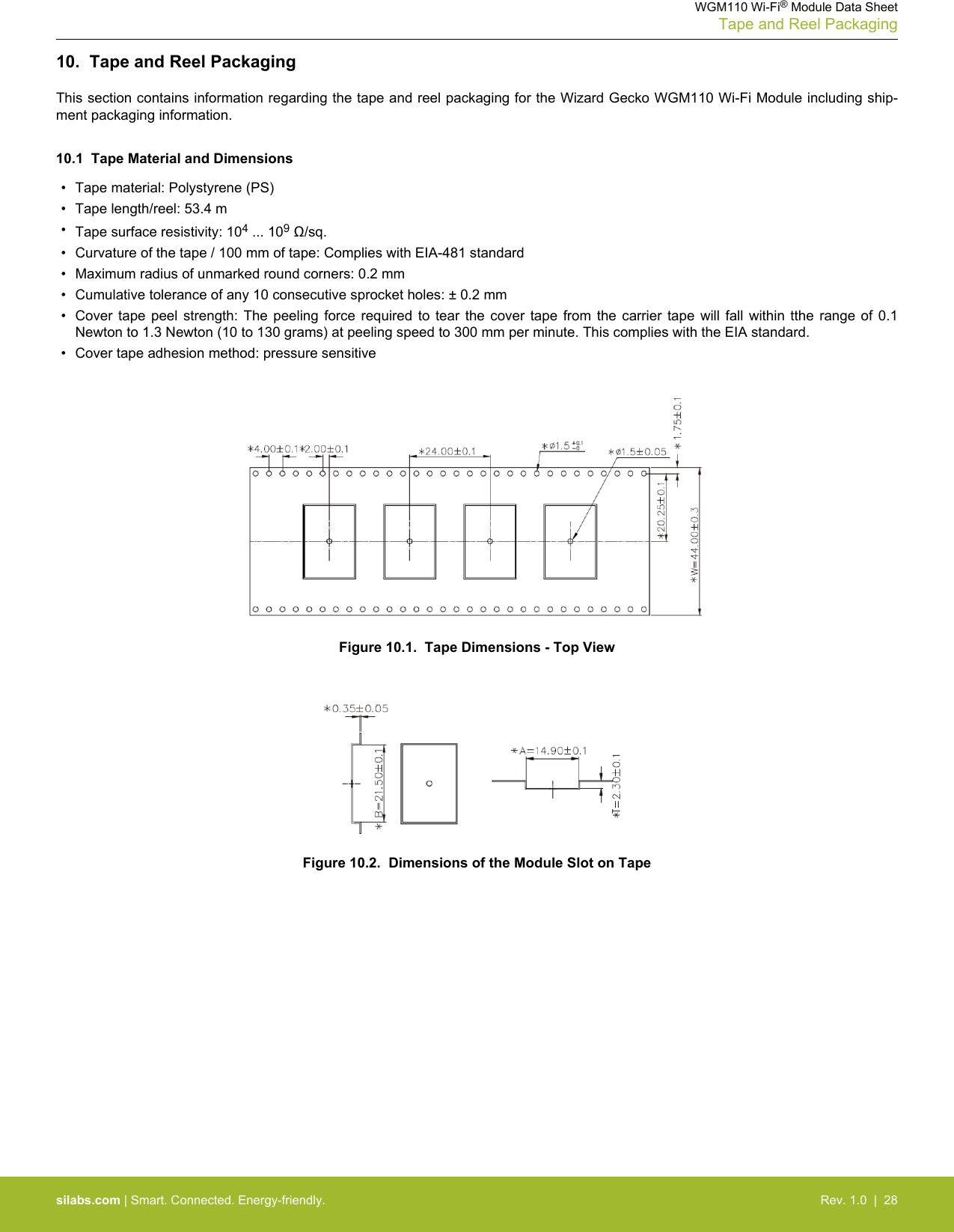
![10.2 Reel Material and Dimensions•Reel material: Polystyrene (PS)• Reel diameter: 13 inches (330 mm)• Number of modules per reel: 500 pcs• Environmental standard of reel materials: Delta Management Standard for Environnment related substances• Disk deformation, folding whitening and mold imperfections: Not allowed• Disk set: consists of two 13 inch (330 mm) rotary round disks and one central axis (100 mm)• Antistatic treatment: Required•Surface resistivity: 108 - 1011 Ω/cm2Figure 10.3. Reel Dimensions - Side ViewSymbol Dimensions [mm]W0 45.0 ± 0.5W1 50.0 ± 1.0Figure 10.4. Central Axis DimensionsWGM110 Wi-Fi® Module Data SheetTape and Reel Packagingsilabs.com | Smart. Connected. Energy-friendly. Rev. 1.0 | 29](https://usermanual.wiki/Silicon-Laboratories-Finland/WGM110.User-Manual/User-Guide-2950759-Page-30.png)
![10.3 Module Orientation in TapeFigure 10.5. Module Orientation in Tape10.4 Moisture Sensitivity LevelWGM110 Module reels are delivered in packing which conforms to MSL3 (Moisture Sensitivity Level 3) requirements.10.5 Tape and Reel Box DimensionsFigure 10.6. Tape and Reel Box DimensionsSymbol Dimensions [mm]W2368W3338W472WGM110 Wi-Fi® Module Data SheetTape and Reel Packagingsilabs.com | Smart. Connected. Energy-friendly. Rev. 1.0 | 30](https://usermanual.wiki/Silicon-Laboratories-Finland/WGM110.User-Manual/User-Guide-2950759-Page-31.png)