Silicon Laboratories Finland WT11 Bluetooth Class I EDR Module User Manual WT11 Data Sheet and manual
Silicon Laboratories Finland Oy Bluetooth Class I EDR Module WT11 Data Sheet and manual
User Manual

WT11
Preliminary Data Sheet
Version 1.4
Thursday,
May 04, 2006

Copyright © 2000-2006 Bluegiga Technologies
All rights reserved.
Bluegiga Technologies assumes no responsibility for any errors, which may appear in this
manual. Furthermore, Bluegiga Technologies reserves the right to alter the hardware,
software, and/or specifications detailed herein at any time without notice, and does not
make any commitment to update the information contained herein. Bluegiga Technologies’
products are not authorized for use as critical components in life support devices or
systems.
The WRAP is a registered trademark of Bluegiga Technologies
The Bluetooth trademark is owned by the Bluetooth SIG Inc., USA, and is licensed to
Bluegiga Technologies.
All other trademarks listed herein are owned by their respective owners.

2
Contents:
1. Device Features Overview .......................................................................... 4
2. General Description.................................................................................... 5
2.1 Physical Outlook..........................................................................................5
2.2 Block Diagram and Descriptions.....................................................................6
2.2.1 BlueCore04 ...........................................................................................6
2.2.2 Crystal .................................................................................................7
2.2.3 Flash....................................................................................................7
2.2.4 Balun ...................................................................................................7
2.2.5 Power amplifier......................................................................................7
2.2.6 Switch ..................................................................................................7
2.2.7 Matching...............................................................................................7
2.2.8 Antenna................................................................................................7
2.2.9 U.FL.....................................................................................................7
2.2.10 USB ..................................................................................................7
2.2.11 Synchronous Serial Interface ................................................................7
2.2.12 UART.................................................................................................7
2.2.13 Audio PCM Interface ............................................................................7
2.2.14 Programmable I/O...............................................................................8
2.2.15 Reset.................................................................................................8
2.2.16 802.11 Coexistence Interface................................................................8
2.3 Applications ................................................................................................8
2.4 Product names and codes .............................................................................9
3. Electrical Charasteristics .......................................................................... 12
4. WT11 PIN description .............................................................................. 13
5. Foot print ................................................................................................. 15
6. Antenna Keep out area ............................................................................. 16
7. WT11-A Physical Dimensions ................................................................... 17
7.1 UART Interface.......................................................................................... 18

3
VERSION HISTORY
Version: Date: Author: Comments:
1.0 11.5.2005 MS Preliminary version
1.1 14.9.2005 PR Dimension update
1.2 30.1.2006 MS Images, dimensions and
interfaces updated.
1.3 6.2.2006 MS Foot print fixed
1.4 2.3.2006 PR Figure 6 added

4
1. DEVICE FEATURES OVERVIEW
• Fully Qualified Bluetooth system v2.0 + EDR, CE and FCC
• Class 1, range up to 300 meters
• Integrated chip antenna or UFL connector
• Industrial temperature range from -40oC to +85oC
• Enhanced Data Rate (EDR) compliant with v2.0.E.2 of specification for both 2Mbps
and 3Mbps modulation modes
• RoHS Compliant
• Full Speed Bluetooth Operation with Full Piconet
• Scatternet Support
• USB version 2.0 compatible
• UART with bypass mode
• Support for 802.11 Coexistence
• 8Mbits of Flash Memory

5
2. GENERAL DESCRIPTION
2.1 Physical Outlook
Figure 1: Physical outlook of WT11-A
Figure 2: Physical outlook of WT11-E
6
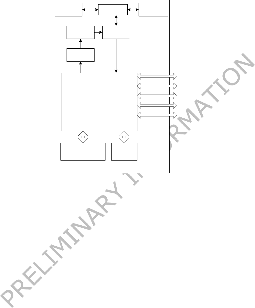
2.2 Block Diagram and Descriptions
+3.3V
U.FL
connector Matching
BlueCore04
8 MBit
Flash Memory
26 MHz
Crystal
UART
SPI
PCM
USB
PIO
WT11
RESET
Chip
antenna
Balun
Power
amplifier Switch
Figure 3: Block Diagram of WT11
2.2.1 BlueCore04
BlueCore4 is a single chip Bluetooth solution which implements the Bluetooth radio
transceiver and also an on chip microcontroller. BlueCore4 implements Bluetooth®
2.0+EDR (Enhanced Data Rate) and it can deliver data rates up to 3 Mbps.
The microcontroller (MCU) on BlueCore04 acts as interrupt controller and event timer run
the Bluetooth software stack and control the radio and host interfaces. A 16-bit reduced
instruction set computer (RISC) microcontroller is used for low power consumption and
efficient use of memory.
BlueCore04 has 48Kbytes of on-chip RAM is provided to support the RISC MCU and is
shared between the ring buffers used to hold voice/data for each active connection and
the general purpose memory required by the Bluetooth stack.

7
2.2.2 Crystal
The crystal oscillates at 26MHz.
2.2.3 Flash
Flash memory is used for storing the Bluetooth protocol stack and Virtual Machine
applications. It can also to the optional external RAM for memory intensive applications.
2.2.4 Balun
Balun changes the balanced input/output signal of the module to unbalanced signal of the
monopole antenna.
2.2.5 Power amplifier
Power amplifier is used to increase the output power to a level required by class 1
specification.
2.2.6 Switch
Switch is used to separate transmission and receiver modes.
2.2.7 Matching
Antenna matching components match the antenna to 50 Ohms and also selects between
chip antenna and UFL connector.
2.2.8 Antenna
The antenna is ACX AT3216 chip antenna.
2.2.9 U.FL
This is a standard U.FL male connector for external antenna possibility.
2.2.10 USB
This is a full speed Universal Serial Bus (USB) interface for communicating with other
compatible digital devices. WT11 acts as a USB peripheral, responding to requests from a
Master host controller such as a PC.
2.2.11 Synchronous Serial Interface
This is a synchronous serial port interface (SPI) for interfacing with other digital devices.
The SPI port can be used for system debugging. It can also be used for programming the
Flash memory.
2.2.12 UART
This is a standard Universal Asynchronous Receiver Transmitter (UART) interface for
communicating with other serial devices.
2.2.13 Audio PCM Interface
The audio pulse code modulation (PCM) Interface supports continuous transmission and
reception of PCM encoded audio data over Bluetooth.

8
2.2.14 Programmable I/O
WT11 has a total of 6 digital programmable I/O terminals. These are controlled by
firmware running on the device.
2.2.15 Reset
This can be used to reset WT11.
2.2.16 802.11 Coexistence Interface
Dedicated hardware is provided to implement a variety of coexistence schemes. Channel
skipping AFH (Adaptive Frequency Hopping), priority signaling, channel signaling and host
passing of channel instructions are all supported. The features are configured in firmware.
Since the details of some methods are proprietary (e.g. Intel WCS) please contact
Bluegiga Technologies for details.
2.3 Applications
WT11 Bluetooth module is designed for:
• Hand held terminals
• Industrial devices
• Point-of-Sale systems
• PCs
• Personal Digital Assistants (PDAs)
• Computer Accessories
• Access Points
• Automotive Diagnostics Units

9
2.4 Product names and codes
iWRAP firmware:
• WT11 with internal chip antenna, iWRAP firmware: WT11-A-AI
• WT11 with UFL connector, iWRAP firmware: WT11-E-AI
HCI firmware:
• WT11 with internal chip antenna, HCI firmware: WT11-A-HCI
• WT11 with UFL connector, HCI firmware: WT11-E-HCI
Notes:
HCI firmware is delivered with USB as host interface!
Custom firmware:
• WT11 with internal chip antenna, custom firmware: WT11-A-C
• WT11 with UFL connector, custom firmware: WT11-E-C
Notes:
Custom firmware requires properly filled custom firmware document or custom
firmware ID.

10
General Specifications
Item Specification
Supply voltage 3.3 V ± 0.1 V regulated voltage. (Noise < 10 mVP-P)
Supply current
Maximum current in TX mode: 170.0mA
Maximum current in RX mode: 170.0mA
Frequency range 2400 MHz … 2483.5 MHz (ISM-Band)
Guard band 2 MHz < F < 3.5 MHz (Europe, Japan, USA)
Carrier frequency 2402 MHz … 2480 MHz, F = 2402 + k MHz, k = 0 … 78
Modulation method GFSK (1 Mbps), Π/4 DQPSK (2Mbps) and 8DQPSK (3Mbps)
Hopping 1600 hops/s, 1 MHz channel space
Maximum data rate
GFSK:
Asynchronous, 723.2 kbps / 57.6 kbps
Synchronous: 433.9 kbps / 433.9 kbps
Π/4 DQPSK:
Asynchronous, 1448.5 kbps / 115.2 kbps
Synchronous: 869.7 kbps / 869.7 kbps
8DQPSK:
Asynchronous, 2178.1 kbps / 177.2 kbps
Synchronous: 1306.9 kbps / 1306.9 kbps
Receiving signal range -82 to -20 dBm (Typical)
Receiver IF frequency 1.5 MHz (Center frequency)
Transmission power
Minimum: -11 …-9 dBm
Maximum +16 … +20 dBm

11
RF input impedance 50 Ω
Baseband crystal OSC 26 MHz
Output interfaces 6 GPIO, PCM, SPI, UART, USB
Operation temperature -40ºC … +85ºC
Storage temperature -40ºC … +105ºC
Compliance Bluetooth specification, version 2.0 + EDR
USB specification USB specification, version 1.2
Table 1: General specifications

12
3. ELECTRICAL CHARASTERISTICS
Rating Min Max
Storage temperature -40°C +150°C
Supply Voltage: VDD 3.2V 3.4V
Table 2: Absolute Maximum Ratings
Operating conditions Min Max
Operating Temperature Range: -40°C +85°C
Supply Voltage: VDD 3.2V 3.4V
Table 3: Recommended Operating Conditions
Digital terminals Min Typ Max Unit
Input voltage
VIL input logic level low (VDD=3.3V) -0.4 +0.8 V
VIH input logic level high 0.7VDD VDD+0.1 V
Output voltage
VOL output logic level low
(VDD=3.3V) (lo = 3.0mA) 0.2 V
VOL output logic level high
(VDD=3.3V) (lo = -3.0mA) VDD-0.2 V
Table 4: Input/Output Terminal Characteristics

13
4. WT11 PIN DESCRIPTION
The PIN description of WT11 is shown in the table below.
No. Pin name I/O Description
1 GND GND Ground
2 3V3 VDD Power supply connection
3 PIO2 I/O Programmable I/O lines
4 PIO3 I/O Programmable I/O lines
5 NRTS O UART RTS (internal pull-up, active low)
6 RXD I UART RX (internal pull down)
7 PCMO O Synchronous 8 kbps data out (internal Pull down)
8 USB_D+ A USB data plus (Internal 22 ohm serial resistor)
9 USB_D- A USB data minus (Internal 22 ohm serial resistor)
10 NCTS I UART CTS (internal pull down, active low)
11 PCMI I Synchronous 8 kbps data in (internal pull-down)
12 PCMC I/O Synchronous data clock (internal pull-down)
13 PCMS I/O Synchronous data strobe (internal pull-down)
14 GND GND Ground
15 GND GND Ground
16 3V3 VDD Power supply connection
17 RES I Reset input (active high)

14
18 PIO6 I/O Programmable I/O lines
19 PIO7 I/O Programmable I/O lines
20 PIO4 I/O Programmable I/O lines
21 NCSB I Chip selection for SPI (internal pull up, active low)
22 SCLK I/O SPI Clock (internal pull down)
23 MISO O SPI data output (pull down)
24 MOSI I SPI data input (pull down)
25 PIO5 I/O Programmable I/O lines
26 TXD O UART TX (internal pull up)
27 NC - NC, not used in WT11 module.
28 GND GND Ground
Table 5: WT11 PIN configuration
Notes: Voltage level of input (I), output (O) and input/output (I/O) pins is 3.3V.

15
5. FOOT PRINT
Figure 4: WT11 foot print and dimension
Figure 5: WT11 pad dimensions
16
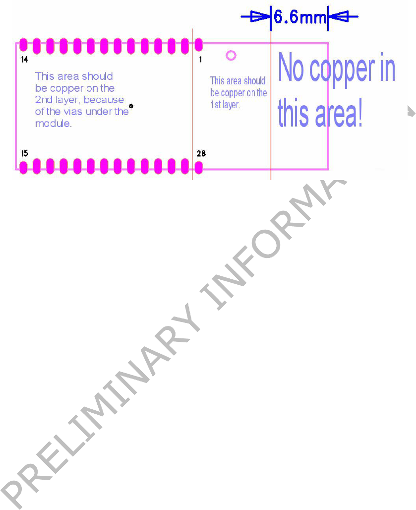
6. ANTENNA KEEP OUT AREA
Figure 6: PCB design around ACX antenna
Figure four above illustrates how PCB design around the antenna of WT11 should be
made. The most important thing is that there is no copper (ground plane or traces)
underneath or in the close proximity of the ACX antenna.
It’s also very important to have grounding vias all the way in the border between ground
plane and free space, as illustrated with black and gray dots in figure 4. This prevents the
RF signal for reflecting back to the PCB and signal lines over there.
For more information, please refer to the WT11 design guide and design references.
17
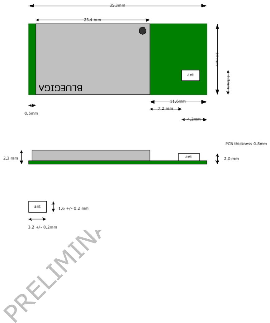
7. WT11-A PHYSICAL DIMENSIONS
Figure 7: WT11-A Dimensions
18
Physical Interfaces
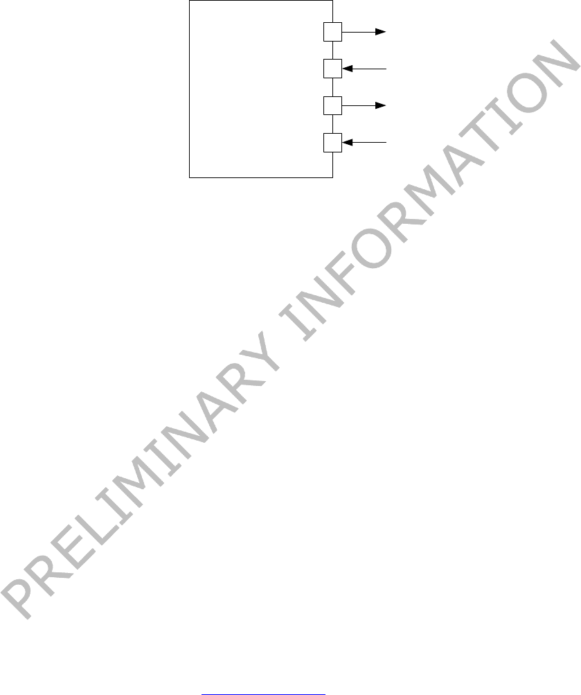
7.1 UART Interface
WT11 Universal Asynchronous Receiver Transmitter (UART) interface provides a simple
mechanism for communicating with other serial devices using the RS232 standard1.
UART_TX
UART_RX
UART_RTS
UART_CTS
WT12
Figure 8: WT11 UART interface
Four signals are used to implement the UART function, as shown in Figure 11.12. When
WT11 is connected to another digital device, UART_RX and UART_TX transfer data
between the two devices. The remaining two signals, UART_CTS and UART_RTS, can be
used to implement RS232 hardware flow control where both are active low indicators. All
UART connections are implemented using CMOS technology and have signaling levels of
0V and VDD_PADS.
Figure 9: WRAP THOR VM Stack
In figure above, the iWRAP software solution is described. In this version of the stack
firmware shown no host processor is required to run the Bluetooth protocol stack. All
software layers, including application software, run on the internal RISC processor in a
protected user software execution environment known as a Virtual Machine (VM).
The host processor interfaces to iWRAP software via one or more of the physical interfaces
which are also shown in the figure above. The most common interfacing is done via UART
interface using the ASCII commands supported by the iWRAP software. With these ASCII
commands the user can access Bluetooth functionality without paying any attention to the
complexity which lies in the Bluetooth protocol stack.
The user may write applications code to run on the host processor to control iWRAP
software with ASCII commands and to develop Bluetooth powered applications.
Notes:
More details of iWRAP software and it’s features can be found from iWRAP User Guide
which can be downloaded from www.bluegiga.com.

19
Federal Communications Commission (FCC) Statement
15.21
You are cautioned that changes or modifications not expressly approved by the part
responsible for compliance could void the user’s authority to operate the equipment.
15.105(b)
This equipment has been tested and found to comply with the limits for a Class B digital
device, pursuant to part 15 of the FCC rules. These limits are designed to provide
reasonable protection against harmful interference in a residential installation. This
equipment generates, uses and can radiate radio frequency energy and, if not installed
and used in accordance with the instructions, may cause harmful interference to radio
communications. However, there is no guarantee that interference will not occur in a
particular installation. If this equipment does cause harmful interference to radio or
television reception, which can be determined by turning the equipment off and on, the
user is encouraged to try to correct the interference by one or more of the following
measures:
-Reorient or relocate the receiving antenna.
-Increase the separation between the equipment and receiver.
-Connect the equipment into an outlet on a circuit different from that to which the receiver
is connected.
-Consult the dealer or an experienced radio/TV technician for help.
Operation is subject to the following two conditions:
1) this device may not cause interference and
2) this device must accept any interference, including interference that may cause
undesired operation of the device.
FCC RF Radiation Exposure Statement:
This equipment complies with FCC radiation exposure limits set forth for an uncontrolled
environment. End users must follow the specific operating instructions for satisfying RF
exposure compliance. This transmitter must not be co-located or operating in conjunction
with any other antenna or transmitter.
Note: The end product shall has the words “Contains Transmitter Module
FCC ID: QOQWT11”

20
Contact Information
Sales: sales@bluegiga.com
Technical support: support@bluegiga.com
http://www.bluegiga.com/techforum/
Orders: orders@bluegiga.com
Head Office / Finland
Phone: +358-9-4355 060
Fax: +358-9-4355 0660
Street Address:
Sinikalliontie 11
02630 ESPOO
FINLAND
Postal address:
P.O. BOX 120
02631 ESPOO, FINLAND
Sales Office / USA
Phone: (781) 556-1039
Bluegiga Technologies, Inc.
99 Derby Street, Suite 200
Hingham, MA 02043