Silicon Laboratories Finland WT11I Bluetooth EDR module User Manual WT11i E Datasheet
Silicon Laboratories Finland Oy Bluetooth EDR module WT11i E Datasheet
User Manual

WT11i-E
DATA SHEET
Monday, 13 February 2012
Version 1.04
Bluegiga Technologies Oy
Copyright © 2000-2012 Bluegiga Technologies
All rights reserved.
Bluegiga Technologies assumes no responsibility for any errors which may appear in this manual.
Furthermore, Bluegiga Technologies reserves the right to alter the hardware, software, and/or specifications
detailed here at any time without notice and does not make any commitment to update the information
contained here. Bluegiga’s products are not authorized for use as critical components in life support devices
or systems.
The WRAP is a registered trademark of Bluegiga Technologies
The Bluetooth trademark is owned by the Bluetooth SIG Inc., USA and is licensed to Bluegiga Technologies.
All other trademarks listed herein are owned by their respective owners.

Bluegiga Technologies Oy
VERSION HISTORY
Version Comment
1.04 Typo corrections
1.03 Page 33: Reset is active high
1.02 Package drawings added
1.01 Ordering information corrected
1.0 Release
Bluegiga Technologies Oy
TABLE OF CONTENTS
1 Ordering Information..................................................................................................................................... 7
2 Pinout and Terminal Description .................................................................................................................. 8
3 Electrical Characteristics ............................................................................................................................ 11
3.1 Absolute Maximum Ratings ................................................................................................................ 11
3.2 Recommended Operating Conditions ................................................................................................. 11
3.3 Current Consumption .......................................................................................................................... 11
3.4 PIO Current Sink and Source Capability ............................................................................................. 12
3.5 Antenna Specification ......................................................................................................................... 12
4 Physical Dimensions .................................................................................................................................. 13
4.1 Package Dimensions .......................................................................................................................... 14
5 Layout Guidelines ....................................................................................................................................... 16
6 UART Interface ........................................................................................................................................... 17
6.1 UART Bypass ...................................................................................................................................... 19
6.2 UART Configuration While Reset is Active ......................................................................................... 19
6.3 UART Bypass Mode ............................................................................................................................ 19
7 USB Interface ............................................................................................................................................. 20
7.1 USB Data Connections ....................................................................................................................... 20
7.2 USB Pull-Up resistor ........................................................................................................................... 20
7.3 USB Power Supply .............................................................................................................................. 20
7.4 Self-Powered Mode ............................................................................................................................. 20
7.5 Bus-Powered Mode ............................................................................................................................. 21
7.6 USB Suspend Current ......................................................................................................................... 22
7.7 USB Detach and Wake-Up Signaling ................................................................................................. 22
7.8 USB Driver .......................................................................................................................................... 23
7.9 USB v2.0 Compliance and Compatibility ............................................................................................ 23
8 Serial Peripheral Interface (SPI) ................................................................................................................. 24
9 PCM Codec Interface ................................................................................................................................. 25
9.1 PCM Interface Master/Slave ............................................................................................................... 25
9.2 Long Frame Sync ................................................................................................................................ 26
9.3 Short Frame Sync ............................................................................................................................... 26
9.4 Multi-slot Operation ............................................................................................................................. 27
9.5 GCI Interface ....................................................................................................................................... 27
9.6 Slots and Sample Formats .................................................................................................................. 28
9.7 Additional Features ............................................................................................................................. 29
9.8 PCM_CLK and PCM_SYNC Generation ............................................................................................ 29
9.9 PCM Configuration .............................................................................................................................. 30
10 I/O Parallel Ports ..................................................................................................................................... 32
Bluegiga Technologies Oy
10.1 PIO Defaults ................................................................................................................................. 32
11 Reset ....................................................................................................................................................... 33
11.1 Pin States on Reset ..................................................................................................................... 33
12 Certifications ........................................................................................................................................... 34
12.1 Bluetooth ...................................................................................................................................... 34
12.2 FCC and IC .................................................................................................................................. 34
12.2.1 FCC et IC ..................................................................................................................................... 36
12.3 CE ................................................................................................................................................ 38
12.4 Qualified Antenna Types for WT11i-E ......................................................................................... 38
13 Contact Information................................................................................................................................. 40

Bluegiga Technologies Oy
WT11i Bluetooth® Module
DESCRIPTION
WT11i is a fully integrated Bluetooth 2.1 + EDR,
class 1 module combining antenna, Bluetooth radio
and an on-board Bluetooth stack. The WT11i
module utilizes Bluegiga's latest generation RF
technology and provides better performance than its
predecessor WT11. For OEM's WT11i offers trouble
free Bluetooth integration for applications where the
best performance is needed and it’s a drop-in
performance upgrade for designs where WT11 is
already used. WT11i comes with Bluegiga's iWRAP
firmware offering the users simple software
integration without the need of Bluetooth protocol or
profile development.
APPLICATIONS:
Hand held terminals
Industrial devices
Point-of-Sale systems
PCs
Personal Digital Assistants (PDAs)
Computer Accessories
Access Points
Automotive Diagnostics Units
FEATURES:
Bluetooth v.2.1 + EDR, class 1
Chip antenna
Radio performance
o Transmit power : +17 dBm
o Receiver sensitivity: -83 dBm
Interfaces:
o USB (2.0 compatible)
o UART with flow control
o 6 x GPIO
o 1 x 8-bit AIO
o 802.11 co-existence
Integrated iWRAP Bluetooth stack
o 12 integrated Bluetooth profiles
o Simple ASCII based host protocol
Standard HCI over UART or USB
Industrial temperature range: -40C to +85C
Bluetooth end product, CE, FCC and IC
and Telec qualified
PHYSICAL OUTLOOK
TBA

Bluegiga Technologies Oy
Page 7 of 40
1 Ordering Information
WT11i-E-HCI
Product series
Fimrware
HCI21= HCI firmware (Bluetooth 2.1 + EDR)
AI3 = iWRAP 3.0.0
AI4 = iWRAP 4.0.0
C = Custom*
HW version
E = u.fl connector

Bluegiga Technologies Oy
Page 8 of 40
2 Pinout and Terminal Description
WT11i
GND
VDD_PA
PIO2
PIO3
UART_RTS#
UART_RX
PCM_OUT
USB+
USB-
UART_CTS#
PCM_IN
PCM_CLK
PCM_SYNC
GND
GND
AIO
UART_TX
PIO5
SPI_MOSI
SPI_MISO
SPI_CLK
SPI_CS#
PIO4
PIO7
PIO6
RESET
VDD
GND
1
2
3
4
5
6
7
8
9
10
11
12
13
14
28
27
26
25
24
23
22
21
20
19
18
17
16
15
Figure 1: WT11i connection diagram
PIN
NUMBER PAD TYPE DESCRIPTION
RESET 17 Input, internal 220kohm
pull-down, internal start
u
p
reset circuitr
y
Active hi
g
h reset. Keep hi
g
h for >5 ms
to cause a reset
GND 1, 14, 15,
28 GND GND
VDD_P
A
2 Supply voltage Supply voltage for the RF power amplifier
VDD 16 Supply voltage Supply voltage for BC4 and the flash
memory
Table 1: Supply and RF Terminal Descriptions

Bluegiga Technologies Oy
Page 9 of 40
PIO PORT PIN
NUMBER PAD TYPE DESCRIPTION
PIO[2] 3 Bi-directional, programmamble
strength internal pull-down/pull-up Programmamble input/output
line
PIO[3] 4 Bi-directional, programmamble
strength internal pull-down/pull-up Programmamble input/output
line
PIO[4] 20 Bi-directional, programmamble
strength internal pull-down/pull-up Programmamble input/output
line
PIO[5] 25 Bi-directional, programmamble
strength internal pull-down/pull-up Programmamble input/output
line
PIO[6] 18 Bi-directional, programmamble
strength internal pull-down/pull-up Programmamble input/output
line
PIO[7] 19 Bi-directional, programmamble
strength internal pull-down/pull-up Programmamble input/output
line
AIO[1] 27 Bi-directional Programmamble analog
in
p
ut
/
out
p
ut line
Table 2: GPIO Terminal Descriptions
SPI
INTERFACE PIN
NUMBER PAD TYPE DESCRIPTION
PCM_OUT 7 CMOS output, tri-state,
weak internal pull-down Synchronous data output
PCM_IN 11 CMOS input, weak
internal pull-down Synchronous data input
PCM_SYNC 13 Bi-directional, weak
internal pull-down Synchronous data sync
PCM_CLK 12 Bi-directional, weak
internal pull-down Synchronous data clock
Table 3: PCM Terminal Descriptions
UART
Interfaces PIN
NUMBER PAD TYPE DESCRIPTION
UART_TX 26 CMOS output, tri-
state, with weak
internal
p
ull-u
p
UART data output, active high
UART_RTS# 5 CMOS output, tri-
state, with weak
internal
p
ull-u
p
UART request to send, active low
UART_RX 6 CMOS input, tri-
state, with weak
internal
p
ull-down UART data input, active high
UART_CTS# 10 CMOS input, tri-
state, with weak
internal
p
ull-down UART clear to send, active low
Table 4: UART Terminal Descriptions

Bluegiga Technologies Oy
Page 10 of 40
USB Interfaces PIN
NUMBER PAD TYPE DESCRIPTION
USB+ 8 Bidirectional USB data plus with selectable internal 1.5k
p
ull-u
p
resistor
USB- 9 Bidirectional USB data minus
Table 5: USB Terminal Descriptions
SPI
INTERFACE PIN
NUMBER PAD TYPE DESCRIPTION
SPI_MOSI 24 CMOS input with weak
internal pull
-
down
SPI data input
SPI_CS# 21 CMOS input with weak
internal pull-up Chip select for Serial Peripheral
Interface, active low
SPI_CLK 22 CMOS input with weak
internal pull-down SPI clock
SPI_MISO 23 CMOS output, tristate,
with weak internal pull
down SPI data output
Table 6: Terminal Descriptions

Bluegiga Technologies Oy
Page 11 of 40
3 Electrical Characteristics
3.1 Absolute Maximum Ratings
Min Max Unit
-40 85 °C
-0.4 3.6 V
VSS-0.4 VDD+0.4 V
Rating
Storage Temperature
Other Terminal Voltages
VDD_PA, VDD
Table 7: Absolute Maximum Ratings
3.2 Recommended Operating Conditions
Min Max Unit
-40 85 °C
3.0 3.6 V
Rating
Operating Temperature Range
VDD_PA, VDD
*)
*) VDD_PA has an effect on the RF output power.
Table 8: Recommended Operating Conditions
3.3 Current Consumption
Packettype Powerlevel MAX AVG Unit
17 dBm 170 72
12 dm 170 54
17 dBm 170 128
12 dm 170 84
2DH5 12 dm 106 93
3DH5 12 dm 106 93
RX - - - 39
Sleep - - - 50 µ
A
Inquiry - 17 dBm 59 mA
DH1
DH5TX mA
Table 9: WT11i Current Consumption
Bluegiga Technologies Oy
Page 12 of 40
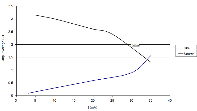
3.4 PIO Current Sink and Source Capability
Figure 2: WT11i PIO Current Drive Capability
3.5 Antenna Specification
Bluegiga Technologies Oy
Page 13 of 40
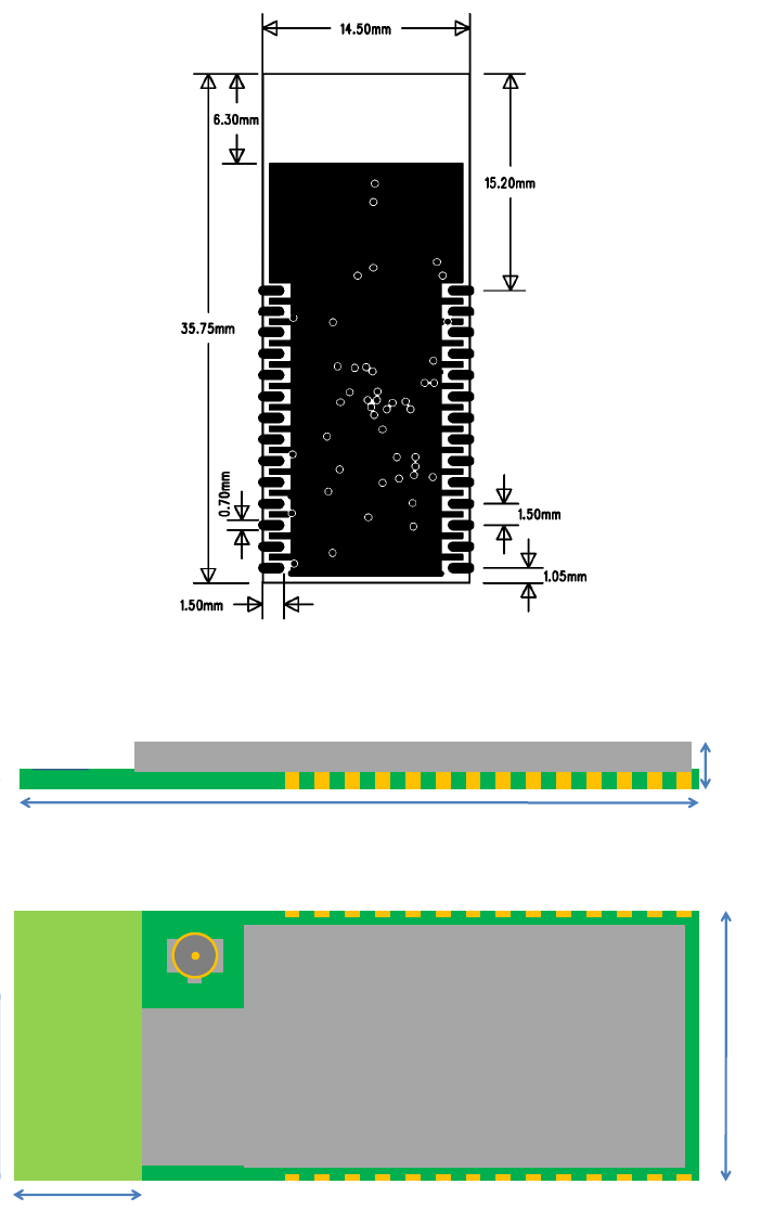
4 Physical Dimensions
Figure 3: Physical dimensions (top view)
2.6m
35.8mm
m
14.5mm
6.3mm
Figure 4: Dimensions of WT11i-E
Bluegiga Technologies Oy
Page 14 of 40
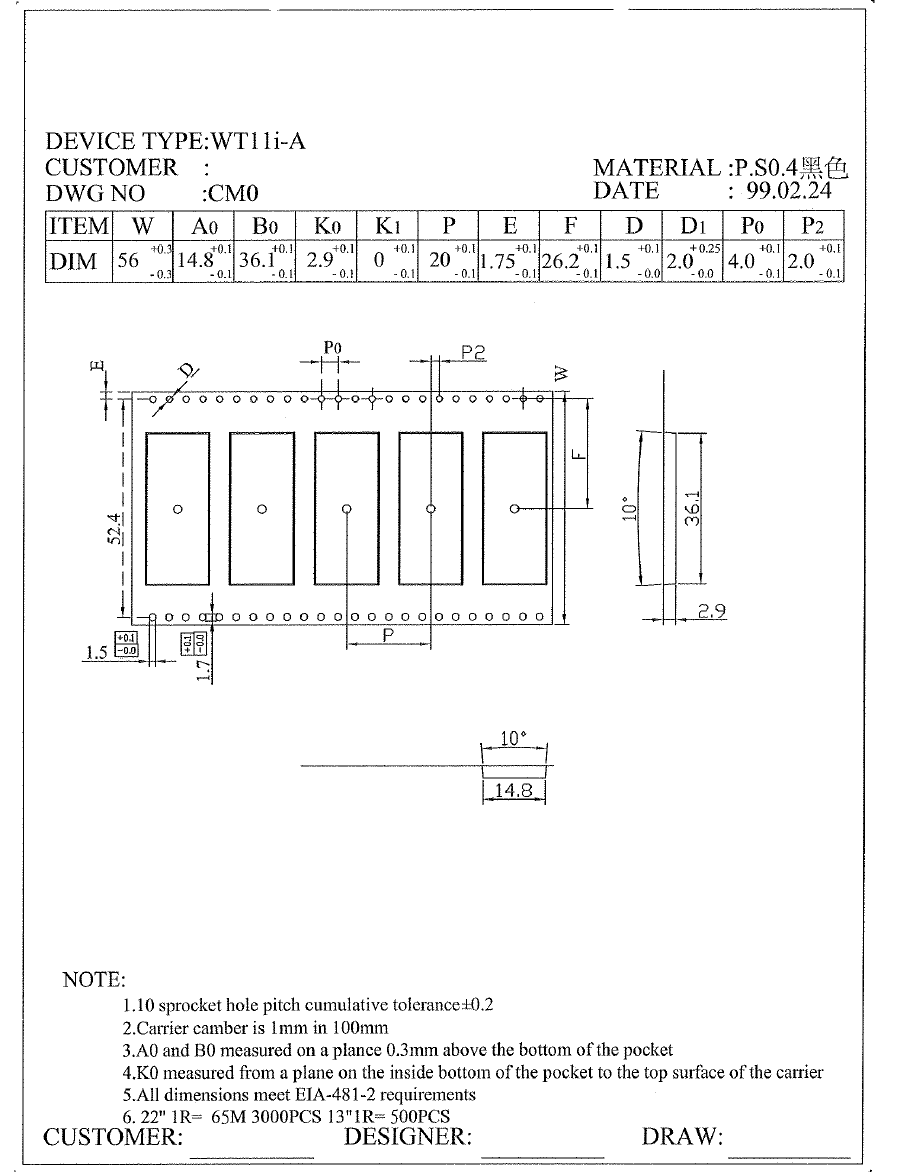
4.1 Package Dimensions
Figure 5: WT11i taping
Bluegiga Technologies Oy
Page 15 of 40
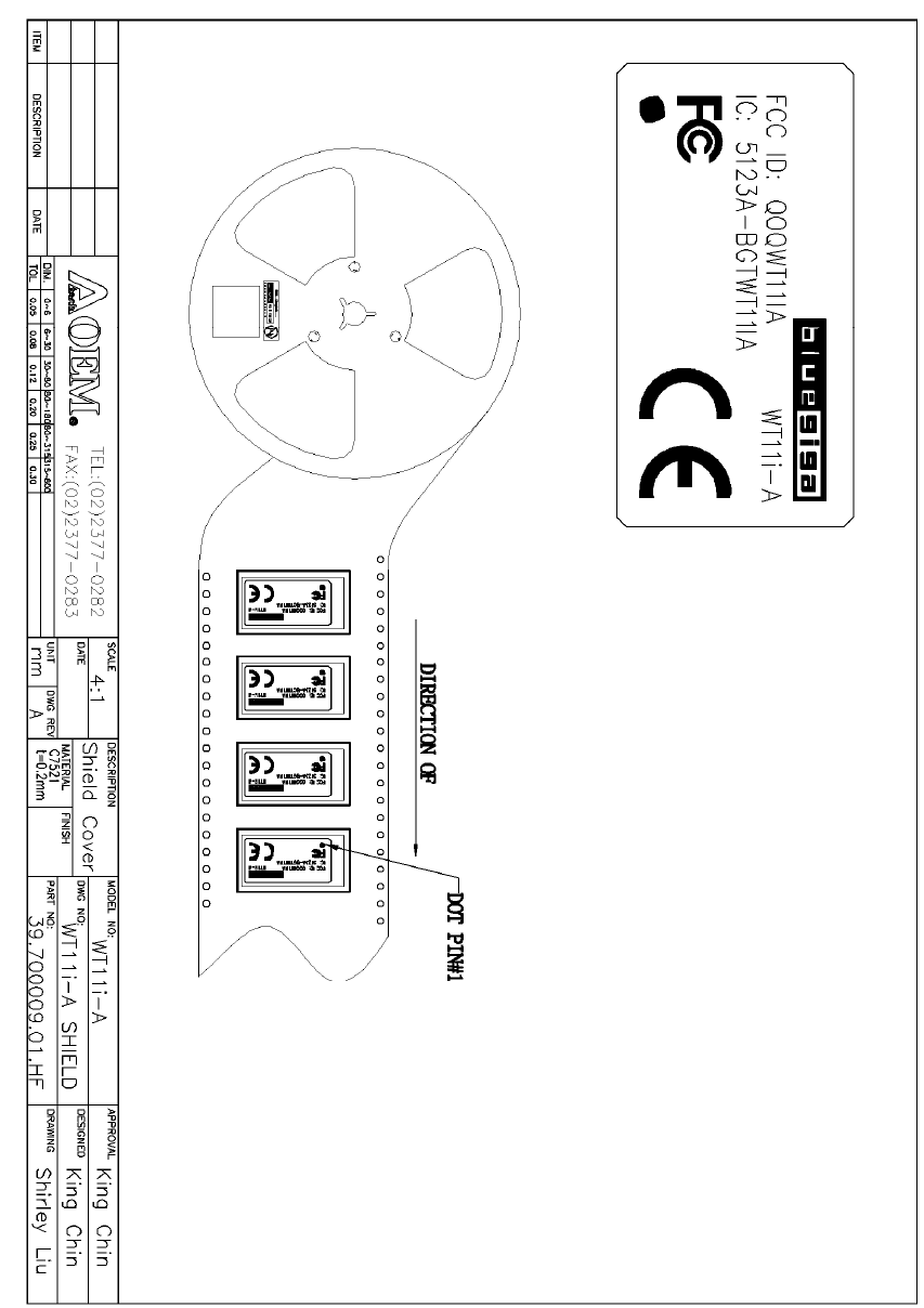
Figure 6: WT11i orientation in the reel
Bluegiga Technologies Oy
Page 16 of 40
5 Layout Guidelines
Use good layout practices to avoid excessive noise coupling to supply voltage traces or sensitive analog
signal traces, such as analog audio signals. If using overlapping ground planes use stitching vias separated
by max 3 mm to avoid emission from the edges of the PCB. Connect all the GND pins directly to a solid GND
plane and make sure that there is a low impedance path for the return current following the signal and supply
traces all the way from start to the end.
A good practice is to dedicate one of the inner layers to a solid GND plane and one of the inner layers to
supply voltage planes and traces and route all the signals on top and bottom layers of the PCB. This
arrangement will make sure that any return current follows the forward current as close as possible and any
loops are minimized.
Signals
GND
Power
Signals
Figure 7: Typical 4-layer PCB construction
Overlapping GND layers without
GND stitching vias Overlapping GND layers with
GND stitching vias shielding the
RF energy
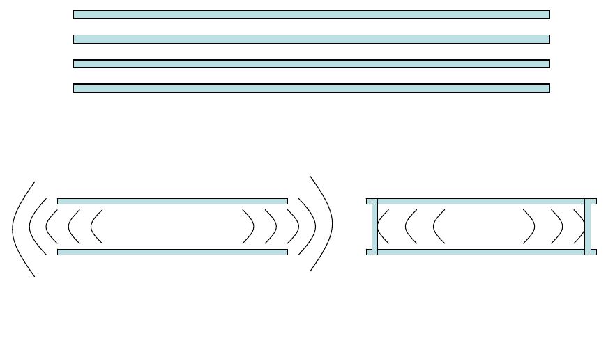
Figure 8: Use of stitching vias to avoid emissions from the edges of the PCB
Bluegiga Technologies Oy
Page 17 of 40
6 UART Interface
This is a standard UART interface for communicating with other serial devices.WT11i UART interface provides
a simple mechanism for communicating with other serial devices using the RS232 protocol.
Four signals are used to implement the UART function. When WT11i is connected to another digital device,
UART_RX and UART_TX transfer data between the two devices. The remaining two signals, UART_CTS and
UART_RTS, can be used to implement RS232 hardware flow control where both are active low indicators. All
UART connections are implemented using CMOS technology and have signalling levels of 0V and VDD.
UART configuration parameters, such as data rate and packet format, are set using WT11i software.
Note:
In order to communicate with the UART at its maximum data rate using a standard PC, an accelerated serial
port adapter card is required for the PC.
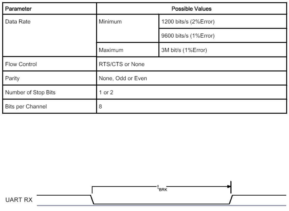
Table 10: Possible UART Settings
The UART interface is capable of resetting WT11i upon reception of a break signal. A break is identified by a
continuous logic low (0V) on the UART_RX terminal, as shown in Figure 9. If tBRK is longer than the value,
defined by PSKEY_HOST_IO_UART_RESET_TIMEOUT, (0x1a4), a reset will occur. This feature allows a
host to initialise the system to a known state. Also, WT11i can emit a break character that may be used to
wake the host.
Figure 9: Break Signal
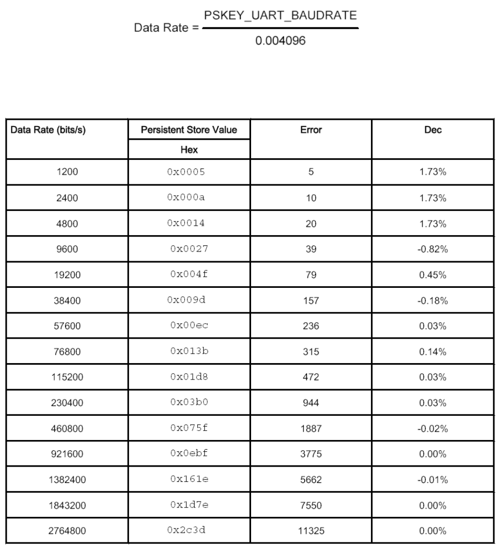
Table 11 shows a list of commonly used data rates and their associated values for
PSKEY_UART_BAUD_RATE (0x204). There is no requirement to use these standard values. Any data rate
within the supported range can be set in the PS Key according to the formula in Equation 1
Bluegiga Technologies Oy
Page 18 of 40
Equation 1: Data Rate
Table 11: Standard Data Rates
Bluegiga Technologies Oy
Page 19 of 40
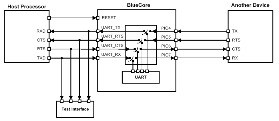
6.1 UART Bypass
Figure 10: UART Bypass Architecture
6.2 UART Configuration While Reset is Active
The UART interface for WT11i while the chip is being held in reset is tristate. This will allow the user to daisy
chain devices onto the physical UART bus. The constraint on this method is that any devices connected to
this bus must tristate when WT11i reset is de-asserted and the firmware begins to run.
6.3 UART Bypass Mode
Alternatively, for devices that do not tristate the UART bus, the UART bypass mode on BlueCore4-External
can be used. The default state of BlueCore4-External after reset is de-asserted; this is for the host UART bus
to be connected to the BlueCore4-External UART, thereby allowing communication to BlueCore4-External via
the UART. All UART bypass mode connections are implemented using CMOS technology and have signalling
levels of 0V and VDD.
In order to apply the UART bypass mode, a BCCMD command will be issued to BlueCore4-External. Upon
this issue, it will switch the bypass to PIO[7:4] as Figure 19 indicates. Once the bypass mode has been
invoked, WT11i will enter the Deep Sleep state indefinitely.
In order to re-establish communication with WT11i, the chip must be reset so that the default configuration
takes effect.
It is important for the host to ensure a clean Bluetooth disconnection of any active links before the bypass
mode is invoked. Therefore, it is not possible to have active Bluetooth links while operating the bypass mode.
The current consumption for a device in UART bypass mode is equal to the values quoted for a device in
standby mode.
Bluegiga Technologies Oy
Page 20 of 40
7 USB Interface
This is a full speed (12Mbits/s) USB interface for communicating with other compatible digital devices. WT11i
acts as a USB peripheral, responding to requests from a master host controller such as a PC.
The USB interface is capable of driving a USB cable directly. No external USB transceiver is required. The
device operates as a USB peripheral, responding to requests from a master host controller such as a PC.
Both the OHCI and the UHCI standards are supported. The set of USB endpoints implemented can behave as
specified in the USB section of the Bluetooth v2.1 + EDR specification or alternatively can appear as a set of
endpoints appropriate to USB audio devices such as speakers.
As USB is a master/slave oriented system (in common with other USB peripherals), WT11i only supports USB
Slave operation.
7.1 USB Data Connections
The USB data lines emerge as pins USB_DP and USB_DN. These terminals are connected to the internal
USB I/O buffers of the BlueCore4-External, therefore, have a low output impedance. To match the connection
to the characteristic impedance of the USB cable, resistors must be placed in series with USB_DP/USB_DN
and the cable.
7.2 USB Pull-Up resistor
WT11i features an internal USB pull-up resistor. This pulls the USB_DP pin weakly high when WT11i is ready
to enumerate. It signals to the PC that it is a full speed (12Mbits/s) USB device.
The USB internal pull-up is implemented as a current source, and is compliant with section 7.1.5 of the USB
specification v1.2. The internal pull-up pulls USB_DP high to at least 2.8V when loaded with a 15k 5% pull-
down resistor (in the hub/host) when VDD_PADS = 3.1V. This presents a Thevenin resistance to the host of
at least 900. Alternatively, an external 1.5k pull-up resistor can be placed between a PIO line and D+ on the
USB cable. The firmware must be alerted to which mode is used by setting PSKEY_USB_PIO_PULLUP
appropriately. The default setting uses the internal pull-up resistor.
7.3 USB Power Supply
The USB specification dictates that the minimum output high voltage for USB data lines is 2.8V. To safely
meet the USB specification, the voltage on the VDD supply terminal must be an absolute minimum of 3.1V.
Bluegiga recommends 3.3V for optimal USB signal quality.
7.4 Self-Powered Mode
In self-powered mode, the circuit is powered from its own power supply and not from the VBUS (5V) line of the
USB cable. It draws only a small leakage current (below 0.5mA) from VBUS on the USB cable. This is the
easier mode for which to design, as the design is not limited by the power that can be drawn from the USB
hub or root port. However, it requires that VBUS be connected to WT11i via a resistor network (Rvb1 and
Rvb2), so WT11i can detect when VBUS is powered up. BlueCore4-External will not pull USB_DP high when
VBUS is off.
Self-powered USB designs (powered from a battery or PSU) must ensure that a PIO line is allocated for USB
pullup purposes. A 1.5k 5% pull-up resistor between USB_DP and the selected PIO line should be fitted to the
design. Failure to fit this resistor may result in the design failing to be USB compliant in self-powered mode.
The internal pull-up in BlueCore is only suitable for bus-powered USB devices, e.g., dongles.
Bluegiga Technologies Oy
Page 21 of 40
Figure 11: USB Connections for Self-Powered Mode
The terminal marked USB_ON can be any free PIO pin. The PIO pin selected must be registered by setting
PSKEY_USB_PIO_VBUS to the corresponding pin number.
Identifier
V
alue Function
R
S
0 to 10 (to be matched per design)** Impedance matching to USB cable
R
vb1
22k 5% VBUS ON sense divider
R
vb2
47k 5% VBUS ON sense divider
Figure 12: USB Interface Component Values
**) WT11i has internal 22 ohm series resistors at the USB lines.
7.5 Bus-Powered Mode
In bus-powered mode, the application circuit draws its current from the 5V VBUS supply on the USB cable.
WT11i negotiates with the PC during the USB enumeration stage about how much current it is allowed to
consume. On power-up the device must not draw more than 100 mA but after being configured it can draw up
to 500 mA.
For WT11i, the USB power descriptor should be altered to reflect the amount of power required. This is
accomplished by setting PSKEY_USB_MAX_POWER (0x2c6). This is higher than for a Class 2 application
due to the extra current drawn by the Transmit RF PA. By default for WT11i the setting is 300 mA.
When selecting a regulator, be aware that VBUS may go as low as 4.4V. The inrush current (when charging
reservoir and supply decoupling capacitors) is limited by the USB specification. See the USB Specification.
Some applications may require soft start circuitry to limit inrush current if more than 10uF is present between
VBUS and GND. The 5V VBUS line emerging from a PC is often electrically noisy. As well as regulation down
to 3.3V and 1.8V, applications should include careful filtering of the 5V line to attenuate noise that is above the
voltage regulator bandwidth. Excessive noise on WT11i supply pins will result in reduced receiver sensitivity
and a distorted RF transmit signal.
Bluegiga Technologies Oy
Page 22 of 40
Figure 13: USB Connections for Bus-Powered Mode
7.6 USB Suspend Current
All USB devices must permit the USB controller to place them in a USB suspend mode. While in USB
Suspend, bus-powered devices must not draw more than 2.5mA from USB VBUS (self-powered devices may
draw more than 2.5mA from their own supply). This current draw requirement prevents operation of the radio
by bus-powered devices during USB Suspend.
When computing suspend current, the current from VBUS through the bus pull-up and pull-down resistors
must be included. The pull-up resistor at the device is 1.5 k. (nominal). The pull-down resistor at the hub is
14.25k. to 24.80k. The pull-up voltage is nominally 3.3V, which means that holding one of the signal lines high
takes approximately 200uA, leaving only 2.3mA available from a 2.5mA budget. Ensure that external LEDs
and/or amplifiers can be turned off by BlueCore4-External. The entire circuit must be able to enter the
suspend mode.
7.7 USB Detach and Wake-Up Signaling
WT11i can provide out-of-band signaling to a host controller by using the control lines called USB_DETACH
and USB_WAKE_UP. These are outside the USB specification (no wires exist for them inside the USB cable),
but can be useful when embedding WT11i into a circuit where no external USB is visible to the user. Both
control lines are shared with PIO pins and can be assigned to any PIO pin by setting
PSKEY_USB_PIO_DETACH and PSKEY_USB_PIO_WAKEUP to the selected PIO number.
USB_DETACH is an input which, when asserted high, causes WT11i to put USB_DN and USB_DP in high
impedance state and turns off the pull-up resistor on DP. This detaches the device from the bus and is
logically equivalent to unplugging the device. When USB_DETACH is taken low, WT11i will connect back to
USB and await enumeration by the USB host.
USB_WAKE_UP is an active high output (used only when USB_DETACH is active) to wake up the host and
allow USB communication to recommence. It replaces the function of the software USB WAKE_UP message
(which runs over the USB cable) and cannot be sent while BlueCore4-External is effectively disconnected
from the bus.
Bluegiga Technologies Oy
Page 23 of 40
Figure 14: USB_Detach and USB_Wake_Up Signals
7.8 USB Driver
A USB Bluetooth device driver is required to provide a software interface between BlueCore4-External and
Bluetooth software running on the host computer. Please, contact support@bluegiga.com for suitable drivers.
7.9 USB v2.0 Compliance and Compatibility
Although WT11i meets the USB specification, CSR cannot guarantee that an application circuit designed
around the module is USB compliant. The choice of application circuit, component choice and PCB layout all
affect USB signal quality and electrical characteristics. The information in this document is intended as a guide
and should be read in association with the USB specification, with particular attention being given to Chapter
7. Independent USB qualification must be sought before an application is deemed USB compliant and can
bear the USB logo. Such qualification can be obtained from a USB plugfest or from an independent USB test
house.
Terminals USB_DP and USB_DN adhere to the USB Specification v2.0 (Chapter 7) electrical requirements.
BlueCore4-External is compatible with USB v2.0 host controllers; under these circumstances the two ends
agree the mutually acceptable rate of 12Mbits/s according to the USB v2.0 specification.

Bluegiga Technologies Oy
Page 24 of 40
8 Serial Peripheral Interface (SPI)
The SPI port can be used for system debugging. It can also be used for programming the Flash memory and
setting the PSKEY configurations. WT11i uses 16-bit data and 16-bit address serial peripheral interface, where
transactions may occur when the internal processor is running or is stopped. SPI interface is connected using
the MOSI, MISO, CSB and CLK pins. Please, contact support@bluegiga.com for detailed information about
the instruction cycle.
Bluegiga Technologies Oy
Page 25 of 40
9 PCM Codec Interface
PCM is a standard method used to digitize audio (particularly voice) for transmission over digital
communication channels. Through its PCM interface, WT11i has hardware support for continual transmission
and reception of PCM data, thus reducing processor overhead for wireless headset applications. WT11i offers
a bidirectional digital audio interface that routes directly into the baseband layer of the on-chip firmware. It
does not pass through the HCI protocol layer.
Hardware on WT11i allows the data to be sent to and received from a SCO connection. Up to three SCO
connections can be supported by the PCM interface at any one time.
WT11i can operate as the PCM interface master generating an output clock of 128, 256 or 512kHz. When
configured as PCM interface slave, it can operate with an input clock up to 2048kHz. WT11i is compatible with
a variety of clock formats, including Long Frame Sync, Short Frame Sync and GCI timing environments.
It supports 13-bit or 16-bit linear, 8-bit µ-law or A-law companded sample formats at 8ksamples/s and can
receive and transmit on any selection of three of the first four slots following PCM_SYNC. The PCM
configuration options are enabled by setting PSKEY_PCM_CONFIG32.
WT11i interfaces directly to PCM audio devices.
NOTE: Analog audio lines are very sensitive to RF disturbance. Use good layout practices to ensure noise
less audio. Make sure that the return path for the audio signals follows the forward current all the way as close
as possible and use fully differential signals when possible. Do not compromise audio routing.
9.1 PCM Interface Master/Slave
When configured as the master of the PCM interface, WT11i generates PCM_CLK and PCM_SYNC.
Figure 15: PCM Interface Master
When configured as the Slave of the PCM interface, WT11i accepts PCM_CLK rates up to 2048kHz.
Bluegiga Technologies Oy
Page 26 of 40
Figure 16: PCM Interface Slave
9.2 Long Frame Sync
Long Frame Sync is the name given to a clocking format that controls the transfer of PCM data words or
samples. In Long Frame Sync, the rising edge of PCM_SYNC indicates the start of the PCM word. When
WT11i is configured as PCM master, generating PCM_SYNC and PCM_CLK, then PCM_SYNC is 8-bits long.
When WT11i is configured as PCM Slave, PCM_SYNC may be from two consecutive falling edges of
PCM_CLK to half the PCM_SYNC rate, i.e., 62.5s long.
Figure 17: Long Frame Sync (Shown with 8-bit Companded Sample)
WT11i samples PCM_IN on the falling edge of PCM_CLK and transmits PCM_OUT on the rising edge.
PCM_OUT may be configured to be high impedance on the falling edge of PCM_CLK in the LSB position or
on the rising edge.
9.3 Short Frame Sync
In Short Frame Sync, the falling edge of PCM_SYNC indicates the start of the PCM word. PCM_SYNC is
always one clock cycle long.
Bluegiga Technologies Oy
Page 27 of 40
Figure 18: Short Frame Sync (Shown with 16-bit Sample)
As with Long Frame Sync, WT11i samples PCM_IN on the falling edge of PCM_CLK and transmits
PCM_OUT on the rising edge. PCM_OUT may be configured to be high impedance on the falling edge of
PCM_CLK in the LSB position or on the rising edge.
9.4 Multi-slot Operation
More than one SCO connection over the PCM interface is supported using multiple slots. Up to three SCO
connections can be carried over any of the first four slots.
Figure 19: Multi-slot Operation with Two Slots and 8-bit Companded Samples
9.5 GCI Interface
WT11i is compatible with the GCI, a standard synchronous 2B+D ISDN timing interface. The two 64kbits/s B
channels can be accessed when this mode is configured.
Bluegiga Technologies Oy
Page 28 of 40
Figure 20: GCI Interface
The start of frame is indicated by the rising edge of PCM_SYNC and runs at 8kHz. With WT11i in Slave mode,
the frequency of PCM_CLK can be up to 4.096MHz.
9.6 Slots and Sample Formats
WT11i can receive and transmit on any selection of the first four slots following each sync pulse. Slot
durations can be either 8 or 16 clock cycles. Durations of 8 clock cycles may only be used with 8-bit sample
formats. Durations of 16 clocks may be used with 8-bit, 13-bit or 16-bit sample formats.
WT11i supports 13-bit linear, 16-bit linear and 8-bit -law or A-law sample formats. The sample rate is
8ksamples/s. The bit order may be little or big endian. When 16-bit slots are used, the 3 or 8 unused bits in
each slot may be filled with sign extension, padded with zeros or a programmable 3-bit audio attenuation
compatible with some Motorola codecs.
Bluegiga Technologies Oy
Page 29 of 40
Figure 21: 16-bit Slot Length and Sample Formats
9.7 Additional Features
WT11i has a mute facility that forces PCM_OUT to be 0. In master mode, PCM_SYNC may also be forced to
0 while keeping PCM_CLK running which some codecs use to control power down.
9.8 PCM_CLK and PCM_SYNC Generation
WT11i has two methods of generating PCM_CLK and PCM_SYNC in master mode. The first is generating
these signals by DDS from BlueCore4-External internal 4MHz clock. Using this mode limits PCM_CLK to 128,
256 or 512kHz and PCM_SYNC to 8kHz. The second is generating PCM_CLK and PCM_SYNC by DDS from
an internal 48MHz clock (which allows a greater range of frequencies to be generated with low jitter but
consumes more power). This second method is selected by setting bit 48M_PCM_CLK_GEN_EN in
PSKEY_PCM_CONFIG32. When in this mode and with long frame sync, the length of PCM_SYNC can be
either 8 or 16 cycles of PCM_CLK, determined by LONG_LENGTH_SYNC_EN in PSKEY_PCM_CONFIG32.
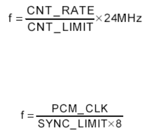
The Equation XXX describes PCM_CLK frequency when being generated using the internal 48MHz clock:
Bluegiga Technologies Oy
Page 30 of 40
Equation 2: PCM_CLK Frequency When Being Generated Using the Internal 48MHz Clock
The frequency of PCM_SYNC relative to PCM_CLK can be set using Equation XXX:
Equation 3: PCM_SYNC Frequency Relative to PCM_CLK
CNT_RATE, CNT_LIMIT and SYNC_LIMIT are set using PSKEY_PCM_LOW_JITTER_CONFIG. As an
example, to generate PCM_CLK at 512kHz with PCM_SYNC at 8kHz, set
PSKEY_PCM_LOW_JITTER_CONFIG to 0x08080177.
9.9 PCM Configuration
The PCM configuration is set using two PS Keys, PSKEY_PCM_CONFIG32 detailed in Table 12 and
PSKEY_PCM_LOW_JITTER_CONFIG in Table 13. The default for PSKEY_PCM_CONFIG32 is 0x00800000,
i.e., first slot following sync is active, 13-bit linear voice format, long frame sync and interface master
generating 256kHz PCM_CLK from 4MHz internal clock with no tri-state of PCM_OUT.

Bluegiga Technologies Oy
Page 31 of 40
Name Bit position Description
-0Set to 0
SLAVE MODE EN 1
0 selects Master mode with internal generation of PCM_CLK and
PCM_SYNC. 1 selects Slave mode requiring externally generated
PCM_CLK and PCM_SYNC. This should be set to 1 if
48M_PCM_CLK_GEN_EN (bit 11) is set.
SHORT SYNC EN 2 0 selects long frame sync (rising edge indicates start of frame), 1
selects short frame sync (falling edge indicates start of frame).
- 3 Set to 0
SIGN EXTENDED
EN 4
0 selects padding of 8 or 13-bit voice sample into a 16- bit slot by
inserting extra LSBs, 1 selects sign extension. When padding is
selected with 3-bit voice sample, the 3 padding bits are the audio gain
setting; with 8-bit samples the 8 padding bits are zeroes.
LSB FIRST EN 5 0 transmits and receives voice samples MSB first, 1 uses LSB first.
TX TRISTATE EN 6 0 drives PCM_OUT continuously, 1 tri-states PCM_OUT immediately
after the falling edge of PCM_CLK in the last bit of an active slot,
assuming the next slot is not active.
TX TRISTATE
RISING EDGE EN 70 tristates PCM_OUT immediately after the falling edge of PCM_CLK
in the last bit of an active slot, assuming the next slot is also not active.
1 tristates PCM_OUT after the rising edge of PCM_CLK.
SYNC SUPPRESS
EN 80 enables PCM_SYNC output when master, 1 suppresses PCM_SYNC
whilst keeping PCM_CLK running. Some CODECS utilize this to enter
a low power state.
GCI MODE EN 9 1 enables GCI mode.
MUTE EN 10 1 forces PCM_OUT to 0.
48M PCM CLK GEN
EN 11
0 sets PCM_CLK and PCM_SYNC generation via DDS from internal 4
MHz clock, as f or BlueCore4-External. 1 sets PCM_CLK and
PCM_SYNC generation via DDS from internal 48 MHz clock.
LONG LENGTH
SYNC EN 12
0 sets PCM_SYNC length to 8 PCM_CLK cycles and 1 sets length to
16 PCM_CLK cycles. Only applies for long frame sync and with
48M_PCM_CLK_GEN_EN set to 1.
-
[
20:16
]
Set to 0b00000.
MASTER CLK RATE [22:21] Selects 128 (0b01), 256 (0b00), 512 (0b10) kHz PCM_CLK frequency
when master and 48M_PCM_CLK_GEN_EN (bit 11) is low.
ACTIVE SLOT
[
26:23
]
Default is 0001. I
g
nored b
y
firmaware
SAMPLE_FORMAT [28:27] Selects between 13 (0b00), 16 (0b01), 8 (0b10) bit sample with 16
cycle slot duration 8 (0b11) bit sample 8 cycle slot duration.
Table 12: PSKEY_PCM_CONFIG32 description
Name Bit position Description
CNT LIMIT [12:0] Sets PCM_CLK counter limit
CNT RATE [23:16] Sets PCM_CLK count rate.
SYNC LIMIT [31:24] Sets PCM_SYNC division relative to PCM_CLK.
Table 13: PSKEY_PCM_LOW_JITTER_CONFIG Description
Bluegiga Technologies Oy
Page 32 of 40
10 I/O Parallel Ports
Six lines of programmable bidirectional input/outputs (I/O) are provided. All the PIO lines are power from VDD.
PIO lines can be configured through software to have either weak or strong pull-ups or pull-downs. All PIO
lines are configured as inputs with weak pull-downs at reset. Any of the PIO lines can be configured as
interrupt request lines or as wake-up lines from sleep modes.
WT11i has a general purpose analogue interface pin AIO[1]. This is used to access internal circuitry and
control signals. It may be configured to provide additional functionality.
Auxiliary functions available via AIO[1] include an 8-bit ADC and an 8-bit DAC. Typically the ADC is used for
battery voltage measurement. Signals selectable at this pin include the band gap reference voltage and a
variety of clock signals: 48, 24, 16, 8MHz and the XTAL clock frequency. When used with analogue signals,
the voltage range is constrained by the analogue supply voltage internally to the module (1.8V). When
configured to drive out digital level signals (e.g., clocks), the output voltage level is determined by VDD.
10.1 PIO Defaults
Bluegiga cannot guarantee that these terminal functions remain the same. Refer to the software release note
for the implementation of these PIO lines, as they are firmware build-specific.

Bluegiga Technologies Oy
Page 33 of 40
11 Reset
WT11i may be reset from several sources: RESET pin, power on reset, a UART break character or via
software configured watchdog timer. The RESET pin is an active high reset and is internally filtered using the
internal low frequency clock oscillator. A reset will be performed between 1.5 and 4.0ms following RESETB
being active. It is recommended that RESET be applied for a period greater than 5ms.
The power on reset occurs when the VDD_CORE supply internally to the module falls below typically 1.5V
and is released when VDD_CORE rises above typically 1.6V. At reset the digital I/O pins are set to inputs for
bidirectional pins and outputs are tri-state.
WT11i has an internal power on reset circuit which holds the module in reset until all the supply voltages have
stabilized. The reset pin must be either floating or connected to high impedance during power on in order for
the power on reset circuit to work properly. If the reset pin is not connected to high impedance during power
on, then one must ensure that the reset is kept active until all the supply voltages have stabilized to prevent
the flash memory getting corrupted.
11.1 Pin States on Reset
PIN NAME STATE
PIO
[
7:2
]
In
p
ut with weak
p
ull-down
PCM_OUT Tri-staed with weak
p
ull-down
PCM_IN In
p
ut with weak
p
ull-down
PCM_SYNC In
p
ut with weak
p
ull-down
PCM_CLK In
p
ut with weak
p
ull-down
UART_TX Out
p
ut tristated with weak
p
ull-u
p
UART_RX In
p
ut with weak
p
ull-down
UART_RTS Out
p
ut tristated with weak
p
ull-u
p
UART_CTS In
p
ut with weak
p
ull-down
USB+ In
p
ut with weak
p
ull-down
USB- In
p
ut with weak
p
ull-down
SPI_CSB In
p
ut with weak
p
ull-down
SPI_CLK In
p
ut with weak
p
ull-down
SPI_MOSI In
p
ut with weak
p
ull-down
SPI_MISO Out
p
ut tristated with weak
p
ull-down
AIO
[
1
]
Out
p
ut
,
drivin
g
low
Table 14: Pin States on Reset

Bluegiga Technologies Oy
Page 34 of 40
12 Certifications
WT11i-E is compliant to the following specifications. At the time of writing this version the official approval for
these specifications is still in the process. Immediately when Bluegiga has received the approval this
disclaimer is removed and the new version of this document is published.
12.1 Bluetooth
WT11i-E module is Bluetooth qualified and listed as a controller subsystem and it is Bluetooth compliant to the
following profiles of the core spec version 2.1/2.1+EDR.
Baseband
HCI
Link Manager
Radio
12.2 FCC and IC
This device complies with Part 15 of the FCC Rules. Operation is subject to the following two conditions:
(1) this device may not cause harmful interference, and
(2) this device must accept any interference received, including interference that may
cause undesired operation.
FCC RF Radiation Exposure Statement:
This equipment complies with FCC radiation exposure limits set forth for an uncontrolled environment. End
users must follow the specific operating instructions for satisfying RF exposure compliance. This transmitter
must not be co-located or operating in conjunction with any other antenna or transmitter. This transmitter is
considered as mobile device and should not be used closer than 20 cm from a human body. To allow portable
use in a known host class 2 permissive change is required. Please contact support@bluegiga.com for detailed
information.
IC Statements:
This device complies with Industry Canada licence-exempt RSS standard(s). Operation is subject to the
following two conditions: (1) this device may not cause interference, and (2) this device must accept any
interference, including interference that may cause undesired operation of the device.
Under Industry Canada regulations, this radio transmitter may only operate using an antenna of a type and
maximum (or lesser) gain approved for the transmitter by Industry Canada. To reduce potential radio
interference to other users, the antenna type and its gain should be so chosen that the equivalent isotropically
radiated power (e.i.r.p.) is not more than that necessary for successful communication.

Bluegiga Technologies Oy
Page 35 of 40
OEM Responsibilities to comply with FCC and Industry Canada Regulations
The WT11i-E module has been certified for integration into products only by OEM integrators under the
following conditions:
The antenna(s) must be installed such that a minimum separation distance of 20cm is maintained
between the radiator (antenna) and all persons at all times.
The transmitter module must not be co-located or operating in conjunction with any other antenna or
transmitter.
As long as the two conditions above are met, further transmitter testing will not be required. However, the
OEM integrator is still responsible for testing their end-product for any additional compliance requirements
required with this module installed (for example, digital device emissions, PC peripheral requirements, etc.).
IMPORTANT NOTE: In the event that these conditions cannot be met (for certain configurations or co-location
with another transmitter), then the FCC and Industry Canada authorizations are no longer considered valid
and the FCC ID and IC Certification Number cannot be used on the final product. In these circumstances, the
OEM integrator will be responsible for re-evaluating the end product (including the transmitter) and either
obtaining a separate FCC and Industry Canada authorization or ask for Bluegiga to make a Class 2
Permissive Change to the listing of the module. With a Class 2 Permissive Change the OEM integrator can
still use the FCC ID and IC Certification Number of the module in the final product and the responsibility of
compliance remains at Bluegiga.
End Product Labeling
The WT11i-E Module is labeled with its own FCC ID and IC Certification Number. If the FCC ID and IC
Certification Number are not visible when the module is installed inside another device, then the outside of the
device into which the module is installed must also display a label referring to the enclosed module. In that
case, the final end product must be labeled in a visible area with the following:
“Contains Transmitter Module FCC ID: QOQWT11I”
“Contains Transmitter Module IC: 5123A-BGTWT11I”
or
“Contains FCC ID: QOQWT11I
“Contains IC: 5123A-BGTWT11I”
The OEM of the WT11i-E module must only use the approved antenna.
The OEM integrator has to be aware not to provide information to the end user regarding how to install or
remove this RF module or change RF related parameters in the user manual of the end product.
To comply with FCC and Industry Canada RF radiation exposure limits for general population, the
antenna(s) used for this transmitter must be installed such that a minimum separation distance of
20cm is maintained between the radiator (antenna) and all persons at all times and must not be co-
located or operating in conjunction with any other antenna or transmitter.

Bluegiga Technologies Oy
Page 36 of 40
12.2.1 FCC et IC
Cet appareil est conforme à l’alinéa 15 des règles de la FCC. Deux conditions sont à respecter lors de
son utilisation :
(1) cet appareil ne doit pas créer d’interférence susceptible de causer un quelconque dommage et,
(2) cet appareil doit accepter toute interférence, quelle qu’elle soit, y compris les interférences
susceptibles d’entraîner un fonctionnement non requis.
Déclaration de conformité FCC d’exposition aux radiofréquences (RF):
Ce matériel respecte les limites d’exposition aux radiofréquences fixées par la FCC dans un environnement
non contrôlé. Les utilisateurs finaux doivent se conformer aux instructions d’utilisation spécifiées afin de
satisfaire aux normes d’exposition en matière de radiofréquence. Ce transmetteur ne doit pas être installé ni
utilisé en concomitance avec une autre antenne ou un autre transmetteur. Ce transmetteur est assimilé à un
appareil mobile et ne doit pas être utilisé à moins de 20 cm du corps humain. Afin de permettre un usage
mobile dans le cadre d’un matériel de catégorie 2, il est nécessaire de procéder à quelques adaptations. Pour
des informations détaillées, veuillez contacter le support technique Bluegiga : support@bluegiga.com.
Déclaration de conformité IC :
Ce matériel respecte les standards RSS exempt de licence d’Industrie Canada. Son utilisation est soumise
aux deux conditions suivantes :
(1) l’appareil ne doit causer aucune interférence, et
(2) l’appareil doit accepter toute interférence, quelle qu’elle soit, y compris les interférences
susceptibles d’entraîner un fonctionnement non requis de l’appareil.
Selon la réglementation d’Industrie Canada, ce radio-transmetteur ne peut utiliser qu’un seul type d’antenne
et ne doit pas dépasser la limite de gain autorisée par Industrie Canada pour les transmetteurs. Afin de
réduire les interférences potentielles avec d’autres utilisateurs, le type d’antenne et son gain devront être
définis de telle façon que la puissance isotrope rayonnante équivalente (EIRP) soit juste suffisante pour
permettre une bonne communication.
Les responsabilités de l’intégrateur afin de satisfaire aux réglementations de la FCC et d’Industrie
Canada :
Les modules WT11i ont été certifiés pour entrer dans la fabrication de produits exclusivement réalisés par des
intégrateurs dans les conditions suivantes :
Bluegiga Technologies Oy
Page 37 of 40
L’antenne (ou les antennes) doit être installée de façon à maintenir à tout instant une distance
minimum de 20cm entre la source de radiation (l’antenne) et toute personne physique.
Le module transmetteur ne doit pas être installé ou utilisé en concomitance avec une autre antenne
ou un autre transmetteur.
Tant que ces deux conditions sont réunies, il n’est pas nécessaire de procéder à des tests supplémentaires
sur le transmetteur. Cependant, l’intégrateur est responsable des tests effectués sur le produit final afin de se
mettre en conformité avec d’éventuelles exigences complémentaires lorsque le module est installé (exemple :
émissions provenant d’appareils numériques, exigences vis-à-vis de périphériques informatiques, etc.) ;
IMPORTANT : Dans le cas où ces conditions ne peuvent être satisfaites (pour certaines configurations ou
installation avec un autre transmetteur), les autorisations fournies par la FCC et Industrie Canada ne sont plus
valables et les numéros d’identification de la FCC et de certification d’Industrie Canada ne peuvent servir pour
le produit final. Dans ces circonstances, il incombera à l’intégrateur de faire réévaluer le produit final
(comprenant le transmetteur) et d’obtenir une autorisation séparée de la part de la FCC et d’Industrie Canada.
Etiquetage du produit final
Chaque module WT11i possède sa propre identification FCC et son propre numéro de certification IC. Si
l’identification FCC et le numéro de certification IC ne sont pas visibles lorsqu’un module est installé à
l’intérieur d’un autre appareil, alors l’appareil en question devra lui aussi présenter une étiquette faisant
référence au module inclus. Dans ce cas, le produit final doit comporter une étiquette placée de façon visible
affichant les mentions suivantes :
« Contient un module transmetteur certifié FCC QOQWT11I »
« Contient un module transmetteur certifié IC 5123A-BGTWT11I »
ou
« Inclut la certification FCC QOQWT11I »
« Inclut la certification IC 5123A-BGTWT11I »
L’intégrateur du module WT11i ne doit utiliser que les antennes répertoriées dans le tableau 21 certifiées pour
ce module.
L’intégrateur est tenu de ne fournir aucune information à l’utilisateur final autorisant ce dernier à installer ou
retirer le module RF, ou bien changer les paramètres RF du module, dans le manuel d’utilisation du produit
final.

Bluegiga Technologies Oy
Page 38 of 40
Afin de se conformer aux limites de radiation imposées par la FCC et Industry Canada, l’antenne (ou
les antennes) utilisée pour ce transmetteur doit être installée de telle sorte à maintenir une distance
minimum de 20cm à tout instant entre la source de radiation (l’antenne) et les personnes physiques.
En outre, cette antenne ne devra en aucun cas être installée ou utilisée en concomitance avec une
autre antenne ou un autre transmetteur.
12.3 CE
WT11i meets the requirements of the standards below and hence fulfills the requirements of EMC Directive
89/336/EEC as amended by Directives 92/31/EEC and 93/68/EEC within CE marking requirement.
EMC (immunity only) EN 301 489-17 V.1.3.3 in accordance with EN 301 489-1 V1.8.1
Radiated emissions EN 300 328 V1.7.1
Safety EN60950-1:2006+A11:2009+A1:2010+A12:2011
12.4 Qualified Antenna Types for WT11i-E
This device has been designed to operate with a standard 2.14 dBi dipole antenna. Any antenna of a different
type or with a gain higher than 2.14 dBi is strictly prohibited for use with this device. Using an antenna of a
different type or gain more than 2.14 dBi will require additional certifications. Please, contact
support@bluegiga.com for more information. The required antenna impedance is 50 ohms.
A
ntenna Type Maximum Gain
Dipole 2.14 dBi
Qualified Antenna Types for WT11i-E
Table 15: Qualified Antenna Types for WT11I-E
To reduce potential radio interference to other users, the antenna type and its gain should be so chosen that
the equivalent isotropically radiated power (e.i.r.p.) is not more than that permitted for successful
communication.
Any standard 2.14 dBi dipole antenna can be used without an additional application to FCC. Table 16 lists
approved antennas for WT11i-E. Any approved antenna listed in table 16 can be used directly with WT11i-E
without any additional approval. Any antenna not listed in table 16 can be used with WT11i-E as long as
detailed information from that particular antenna is provided to Bluegiga for approval. Specification of each
antenna used with WT11i-E will be filed by Bluegiga as a Class 1 Permissive Change. Please, contact
support@bluegiga.com for more information.

Bluegiga Technologies Oy
Page 39 of 40
Item Manufacturer Manufacturers part number
Measure
d Gain
(dBi)
Specifie
d Gain
(dBi)
Measure Total
Efficiency (%)
1 Pulse W1030 1
2 dBi 70 - 80
2 Linx Technologies Inc ANT-2.4-CW-CT-SMA 1.3
2 dBi 77
3 EAD EA-79A 0.4
2 dBi 60
4 Antenova B4844/B6090 1.4
2 dBi 76 - 82
5 Litecon CAR-ATR-187-001 0.8
2 dBi 60 - 70
Table 16: Approved Antennas For WT11i-E

Bluegiga Technologies Oy
Page 40 of 40
13 Contact Information
Sales: sales@bluegiga.com
Technical support: support@bluegiga.com
http://techforum.bluegiga.com
Orders: orders@bluegiga.com
WWW: www.bluegiga.com
www.bluegiga.hk
Head Office / Finland:
Phone: +358-9-4355 060
Fax: +358-9-4355 0660
Sinikalliontie 5A
02630 ESPOO
FINLAND
Postal address / Finland:
P.O. BOX 120
02631 ESPOO
FINLAND
Sales Office / USA:
Phone: +1 770 291 2181
Fax: +1 770 291 2183
Bluegiga Technologies, Inc.
3235 Satellite Boulevard, Building 400, Suite 300
Duluth, GA, 30096, USA
Sales Office / Hong-Kong:
Phone: +852 3182 7321
Fax: +852 3972 5777
Bluegiga Technologies, Inc.
19/F Silver Fortune Plaza, 1 Wellington Street,
Central Hong Kong