Silicon Laboratories Finland WT11U WT11U long range Bluetooth 2.1+EDR module User Manual Product Data Sheet
Silicon Laboratories Finland Oy WT11U long range Bluetooth 2.1+EDR module Product Data Sheet
Users manual

WT11u
DATA SHEET
Monday, 21 November 2016
Version 0.9.2

Silicon Laboratories Finland Oy
VERSION HISTORY
Version
Comment
0.8
Initial versions
0.81
Ordering information updated
0.9
Reformatted tables, many WT11i->WT11u updates
0.9.1
Rest of tables reformatted
0.9.2
Updated dimension drawings
Silicon Laboratories Finland Oy
TABLE OF CONTENTS
1 Ordering Information......................................................................................................................................6
2 Pinout and Terminal Description ...................................................................................................................7
3 Electrical Characteristics ............................................................................................................................ 10
3.1 Absolute Maximum Ratings ................................................................................................................ 10
3.2 Recommended Operating Conditions ................................................................................................. 10
3.3 Input / Output Terminal Characteristics .............................................................................................. 11
3.3.1 Input/Output Terminal Characteristics (Digital) ............................................................................ 11
3.3.2 Input/Output Terminal Characteristics (USB) .............................................................................. 12
3.4 PIO Current Sink and Source Capability ............................................................................................. 13
3.5 Transmitter Performance For BDR ..................................................................................................... 14
3.6 Receiver Performance ........................................................................................................................ 14
3.7 Current Consumption .......................................................................................................................... 15
3.8 WT11u-A Antenna Specification ......................................................................................................... 16
4 Physical Dimensions .................................................................................................................................. 19
4.1 Package Drawings .............................................................................................................................. 21
5 Layout Guidelines ....................................................................................................................................... 23
6 UART Interface ........................................................................................................................................... 26
6.1 UART Bypass ...................................................................................................................................... 28
6.2 UART Configuration While Reset is Active ......................................................................................... 28
6.3 UART Bypass Mode ............................................................................................................................ 28
7 USB Interface ............................................................................................................................................. 29
7.1 USB Data Connections ....................................................................................................................... 29
7.2 USB Pull-Up resistor ........................................................................................................................... 29
7.3 USB Power Supply .............................................................................................................................. 29
7.4 Self-Powered Mode ............................................................................................................................. 29
7.5 Bus-Powered Mode ............................................................................................................................. 30
7.6 USB Suspend Current ......................................................................................................................... 31
7.7 USB Detach and Wake-Up Signaling.................................................................................................. 31
7.8 USB Driver .......................................................................................................................................... 32
7.9 USB v2.0 Compliance and Compatibility ............................................................................................ 32
8 Serial Peripheral Interface (SPI) ................................................................................................................. 33
9 PCM Codec Interface ................................................................................................................................. 34
9.1 PCM Interface Master/Slave ............................................................................................................... 34
9.2 Long Frame Sync ................................................................................................................................ 35
9.3 Short Frame Sync ............................................................................................................................... 35
9.4 Multi-slot Operation ............................................................................................................................. 36
9.5 GCI Interface ....................................................................................................................................... 36
Silicon Laboratories Finland Oy
9.6 Slots and Sample Formats .................................................................................................................. 37
9.7 Additional Features ............................................................................................................................. 38
9.8 PCM_CLK and PCM_SYNC Generation ............................................................................................ 38
9.9 PCM Configuration .............................................................................................................................. 39
10 I/O Parallel Ports ..................................................................................................................................... 42
10.1 PIO Defaults ................................................................................................................................. 42
11 Reset ....................................................................................................................................................... 43
11.1 Pin States on Reset ..................................................................................................................... 44
12 Certifications ........................................................................................................................................... 45
12.1 Bluetooth ...................................................................................................................................... 45
12.2 FCC and IC .................................................................................... Error! Bookmark not defined.
12.2.1 FCC et IC ....................................................................................... Error! Bookmark not defined.
12.3 CE ................................................................................................................................................ 48
12.4 MIC Japan .................................................................................................................................... 48
12.5 KCC (Korea)................................................................................................................................. 48
12.6 Anatel ........................................................................................................................................... 49
12.7 Qualified Antenna Types for WT11u-E ........................................................................................ 50
12.8 Moisture Sensitivity Level (MSL).................................................................................................. 50
Silicon Laboratories Finland Oy
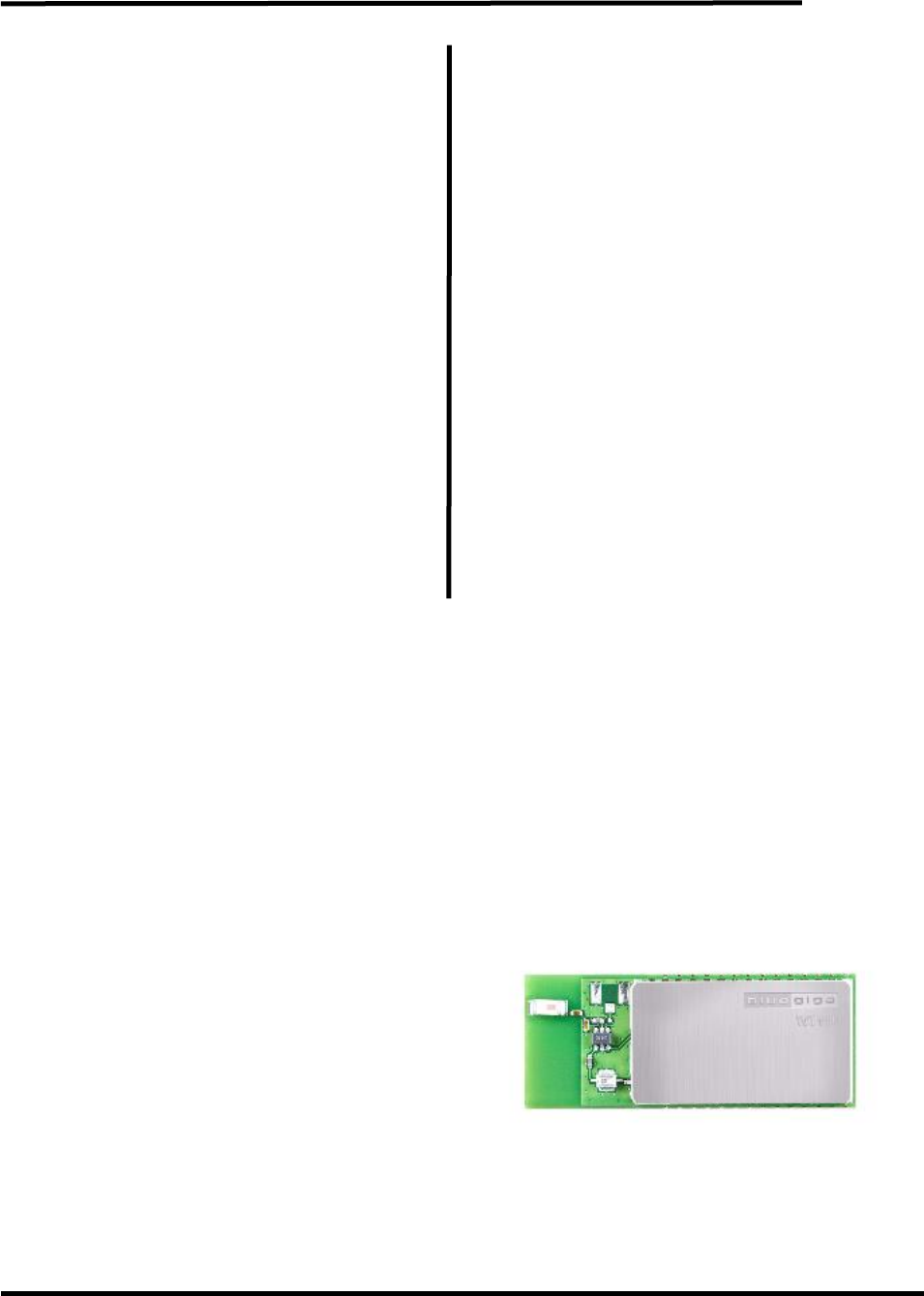
WT11u Bluetooth® Module
DESCRIPTION
WT11u is a fully integrated Bluetooth 2.1 +
EDR, class 1 module combining
antenna, Bluetooth radio and an on-board
iWRAP Bluetooth stack. Silicon Labs WT11u
provides an ideal solution for developers that
want to quickly integrate long range and
high performance Bluetooth wireless
technology to their design without
investing several months into Bluetooth radio
and stack development. WT11u provides a
100dB link budget ensuring long rage and
robust Bluetooth connectivity. WT11u uses
Silicon Labs’ iWRAP Bluetooth stack, which is
an embedded Bluetooth stack implementing
13 different Bluetooth profiles and Apple iAP
connectivity. By using WT11u combined with
iWRAP Bluetooth stack and Silicon Labs’
excellent technical support designers ensure
quick time to market, low development costs
and risk.
APPLICATIONS:
Industrial and M2M
Point-of-Sale devices
Computer Accessories
KEY FEATURES:
Radio features:
Bluetooth v.2.1 + EDR
Bluetooth class 1 radio
Transmit power: +17 dBm
Receiver sensitivity: -84 dBm (DH5)
Range: 350 meters line-of-sight
Integrated chip antenna or U.FL
connector
Hardware features:
UART and USB host interfaces
802.11 co-existence interface
6 software programmable IO pins
Operating voltage: 2.7V to 3.6V
Temperature range: -40C to +85C
Dimensions: 35.75 x 14.50 x 2.6 mm
Qualifications:
Bluetooth
CE
FCC
IC
Japan
PHYSICAL OUTLOOK

Silicon Laboratories Finland Oy
Page 6 of 51
1 Ordering Information
Firmware
U.FL Connector
Internal chip antenna
iWRAP 5.6 firmware, reel
WT11u-E-AI56
WT11u-A-AI56
iWRAP 5.5 firmware, reel
WT11u-E-AI55
WT11u-A-AI55
HCI firmware, BT2.1 + EDR, reel
WT11u-E-HCI21001
WT11u-A-HCI21001
iWRAP 5.6 firmware with iAP, reel
WT11u-E-AI56IAP
WT11u-A-AI56IAP
iWRAP 5.6 firmware, cut reel
WT11u-E-AI56C
WT11u-A-AI56C
iWRAP 5.5 firmware, cut reel
WT11u-E-AI55C
WT11u-A-AI55C
HCI firmware, BT2.1 + EDR, cut reel
WT11u-E-HCI21001C
WT11u-A-HCI21001C
iWRAP 5.6 firmware with iAP, cut reel
WT11u-E-AI56IAPC
WT11u-A-AI56IAPC
Table 1: Ordering information
Silicon Laboratories Finland Oy
Page 7 of 51
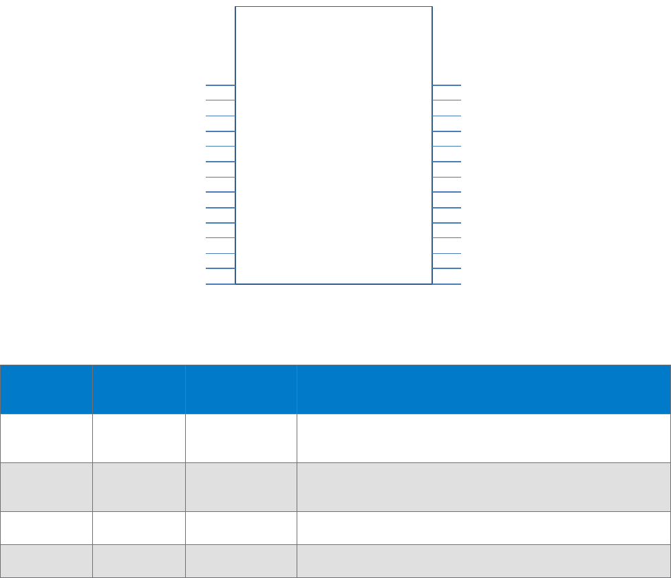
2 Pinout and Terminal Description
Figure 1: WT11u connection diagram
Pad name
Pad
number
Pad type
Description
RESET
17
Input
Reset input, active high, internal 220kohm pull-down. Keep
high for >5ms for reset
GND
1, 14, 15, 28
GND
Ground connection, connect all to a ground plane with
minimal trace lengths
VDD_PA
2
Supply voltage
Supply voltage for RF power amplifier
VDD
16
Supply voltage
Chipset supply voltage
Table 2: Supply and RF Terminal Descriptions
WT11i
GND
VDD_PA
PIO2
PIO3
UART_RTS#
UART_RX
PCM_OUT
USB+
USB-
UART_CTS#
PCM_IN
PCM_CLK
PCM_SYNC
GND
GND
AIO
UART_TX
PIO5
SPI_MOSI
SPI_MISO
SPI_CLK
SPI_CS#
PIO4
PIO7
PIO6
RESET
VDD
GND
1
2
3
4
5
6
7
8
9
10
11
12
13
14
28
27
26
25
24
23
22
21
20
19
18
17
16
15
Silicon Laboratories Finland Oy
Page 8 of 51
PIO signal
Pad number
Description
PIO[2]
3
Bi-directional digital in/out with programmable strength and pull-up/pull-
down
PIO[3]
4
Bi-directional digital in/out with programmable strength and pull-up/pull-
down
PIO[4]
20
Bi-directional digital in/out with programmable strength and pull-up/pull-
down
PIO[5]
25
Bi-directional digital in/out with programmable strength and pull-up/pull-
down
PIO[6]
18
Bi-directional digital in/out with programmable strength and pull-up/pull-
down
PIO[7]
19
Bi-directional digital in/out with programmable strength and pull-up/pull-
down
AIO[1]
27
Bi-directional analog in/out
Table 3: GPIO Terminal Descriptions
PCM signal
Pad number
Pad type
Description
PCM_OUT
7
Output, weak internal pull-down
Synchronous data output
PCM_IN
11
Input, weak internal pull-down
Synchronous data input
PCM_SYNC
13
Bi-directional, weak internal pull-down
Synchronous data sync
PCM_CLK
12
Bi-directional, weak internal pull-down
Synchronous data clock
Table 4: PCM Terminal Descriptions
Silicon Laboratories Finland Oy
Page 9 of 51
UART signal
Pad number
Pad type
Description
UART_TX
26
Output, weak internal
pull-up
UART data output, active
high
UART_RTS#
5
Output, weak internal
pull-up
UART request to send,
active low
UART_RX
6
Input, weak internal pull-
down
UART data input, active
high
UART_CTS#
10
Input, weak internal pull-
down
UART clear to send,
active low
Table 5: UART Terminal Descriptions
USB signal
Pad number
Pad type
Description
USB+
8
Bidirectional
USB data line with internal 1.5kohm pull-up
USB-
9
Bidirectional
USB data line
Table 6: USB Terminal Descriptions
SPI signal
Pad
number
Pad type
Description
SPI_MOSI
24
Input, weak internal pull-down
SPI data input
SPI_CS#
21
Input, weak internal pull-up
Chip select, active low
SPI_CLK
22
Input, weak internal pull-down
SPI clock
SPI_MISO
23
Output, weak internal pull-down
SPI data output
Table 7: Terminal Descriptions

Silicon Laboratories Finland Oy
Page 10 of 51
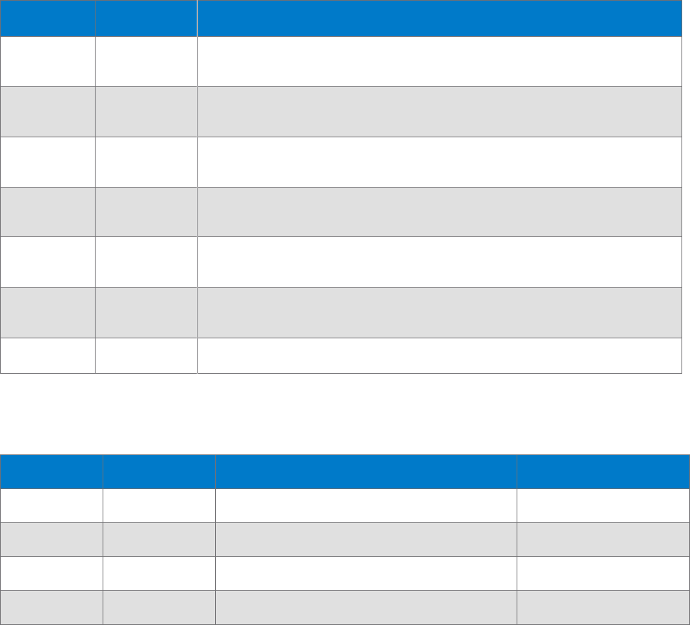
3 Electrical Characteristics
3.1 Absolute Maximum Ratings
Specification
Min
Max
Unit
Storage temperature
-40
85
°C
VDD_PA, VDD
-0.4
3.6
V
Other terminal voltages
VSS-0.4
VDD+0.4
V
Table 8: Absolute Maximum Ratings
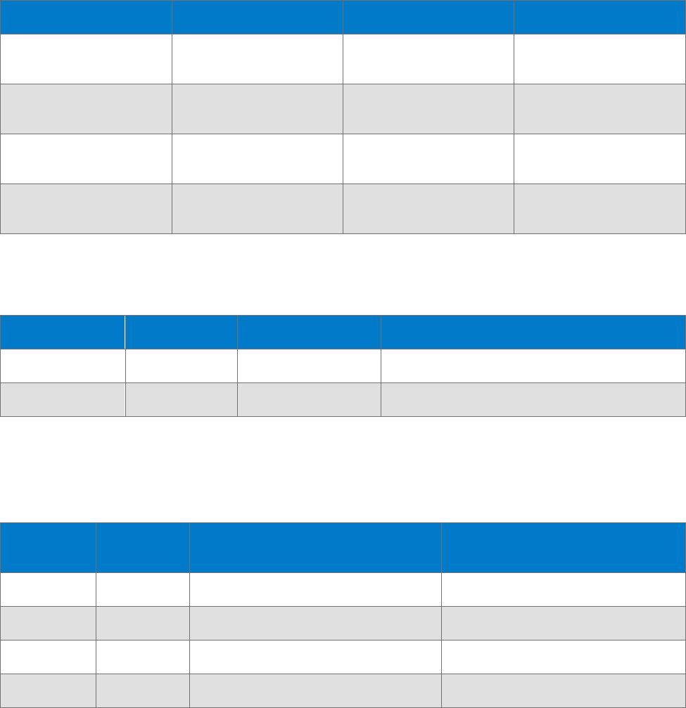
3.2 Recommended Operating Conditions
Specification
Min
Max
Unit
Operating temperature
-40
85
°C
VDD_PA*, VDD
3.0
3.6
V
*) VDD_PA has an effect on the RF output power.
Table 9: Recommended Operating Conditions
Silicon Laboratories Finland Oy
Page 11 of 51
3.3 Input / Output Terminal Characteristics
3.3.1 Input/Output Terminal Characteristics (Digital)
Digital Terminals
Min
Typ
Max
Unit
Input Voltage Levels
VIL input logic level low
2.7 V ≤ VDD ≤ 3.0 V
-0.4
-
0.8
V
1.7 V ≤ VDD ≤ 1.9 V
-0.4
-
0.4
V
VIH input logic level high
0.7 VDD
-
VDD + 0.4
V
Output Voltage Levels
VOL output logic level low
(IO = 4.0 mA) 2.7V ≤ VDD ≤ 3.0 V
-
-
0.2
V
VOL output logic level low
(IO = 4.0 mA) 1.7V ≤ VDD ≤ 1.9
-
-
0.4
V
VOL output logic level high
(IO = 4.0 mA) 2.7V ≤ VDD ≤ 3.0
VDD - 0.2
-
V
VOL output logic level high
(IO = 4.0 mA) 1.7V ≤ VDD ≤ 1.9
VDD - 0.4
-
V
Input and Tristate Current with
Strong pull-up
-100
-40
-10
µA
Strong pull-down
10
40
100
µA
Weak pull-up
-5.0
-1.0
-0.2
µA
Weak pull-down
0.2
1.0
5.0
µA
I/O pad leakage current
-1
0
1
µA
CI input capacitance
1.0
-
5.0
pF

Silicon Laboratories Finland Oy
Page 12 of 51
3.3.2 Input/Output Terminal Characteristics (USB)
USB Terminals
Min
Typ
Max
Unit
VDD_USB for correct USB operation
3.1
3.6
V
Input Threshold
VIL input logic level log
-
-
0.3VDD_USB
V
VIH input logic level high
0.7VDD_USB
-
-
V
Silicon Laboratories Finland Oy
Page 13 of 51
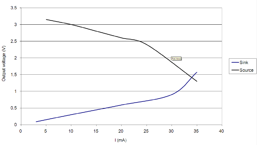
3.4 PIO Current Sink and Source Capability
Figure 2: WT11u PIO Current Drive Capability

Silicon Laboratories Finland Oy
Page 14 of 51
3.5 Transmitter Performance For BDR
RF characteristic
Min
Typ
Max
Bluetooth specification
Unit
Max transmit power
16
17
18.5
<20
dBm
Transmit power variation over temperature
range
TBD
dB
Transmit power variation over supply
voltage range
TBD
dB
Transmit power variation over frequency
range
TBD
dB
Transmit power control range
TBD
17
dB
20dB bandwidth for modulated carrier
TBD
<1000
kHz
ACP
F = F0 ± 2MHz
TBD
-20
dBc
F = F0 ± 3MHz
TBD
-40
dBc
F = F0 > 3MHz
TBD
-40
dBc
Drift rate
TBD
±25
kHz
ΔF1avg
TBD
140 to 175
kHz
ΔF1max
TBD
140 to 175
kHz
ΔF2avg / ΔF1avg
TBD
>=0.8
Table 10: Transmitter performance for BDR (room temperature, VDD=3.3V)
TBD
Figure 3: Typical TX power as a function of VDD_PA
3.6 Receiver Performance
Antenna gain not taken into account
Silicon Laboratories Finland Oy
Page 15 of 51
Characteristic, VDD=3.3V, room temperature
Packet type
Typ
Bluetooth
specification
Unit
Sensitivity for 0.1% BER
DH1
TBD
-70
dBm
DH5
-85
dBm
2-DH1
TBD
dBm
2-DH5
TBD
dBm
3-DH1
TBD
dBm
3-DH5
TBD
dBm
Sensitivity variation over temperature range
TBD
dBm
3.7 Current Consumption
Operating mode
Peak
Average
Unit
Stand-by, page mode 0
TBD
mA
TX 3-DH5
TBD
mA
TX 2-DH5
TBD
mA
TX DH5
TBD
mA
RX
TBD
mA
Deep sleep
TBD
mA
Inquiry
TBD
mA
Table 11: WT11u Current Consumption
Silicon Laboratories Finland Oy
Page 16 of 51
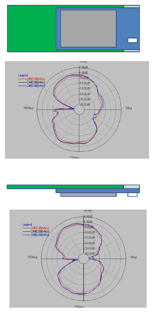
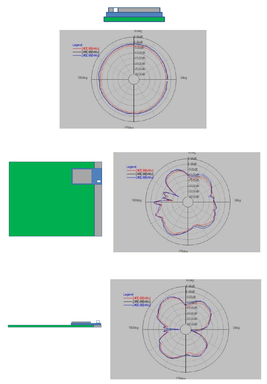
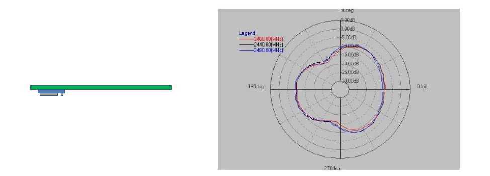
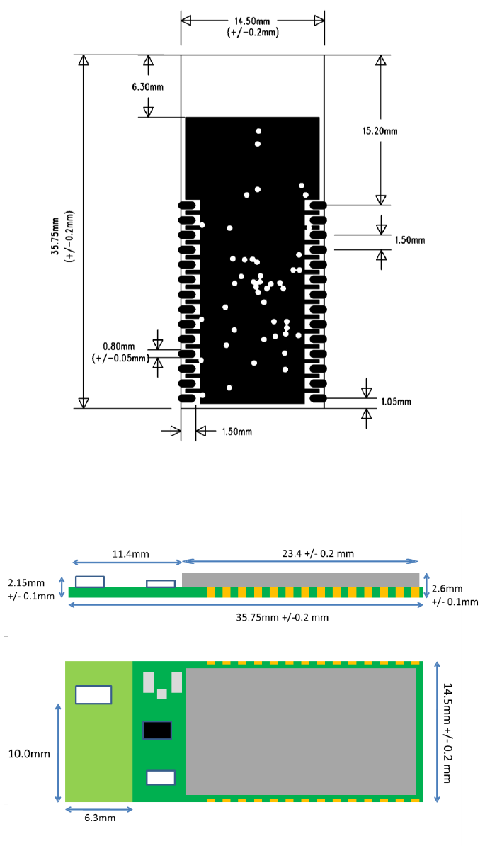
3.8 WT11u-A Antenna Specification
WT11u-A uses a monopole type on a chip antenna with maximum gain of 0.5 dBi. The radiation pattern and the
total radiated efficiency are dependent on the layout and any metal around the antenna has an effect on the
radiation characteristics. Typically the efficiency is 30 … 50%.
Figure 4: Antenna radiation pattern in a USB dongle layout
Figure 5: Antenna radiation pattern in a USB dongle layout
WT11i-A
Silicon Laboratories Finland Oy
Page 17 of 51
Figure 6: Antenna radiation pattern in a USB dongle layout
Figure 7: Antenna radiation pattern in the WT11 evaluation kit
Figure 8: Antenna radiation pattern in the WT11 evaluation kit
WT11i
Silicon Laboratories Finland Oy
Page 18 of 51
Figure 9: Antenna radiation pattern in the WT11 evaluation kit
Silicon Laboratories Finland Oy
Page 19 of 51
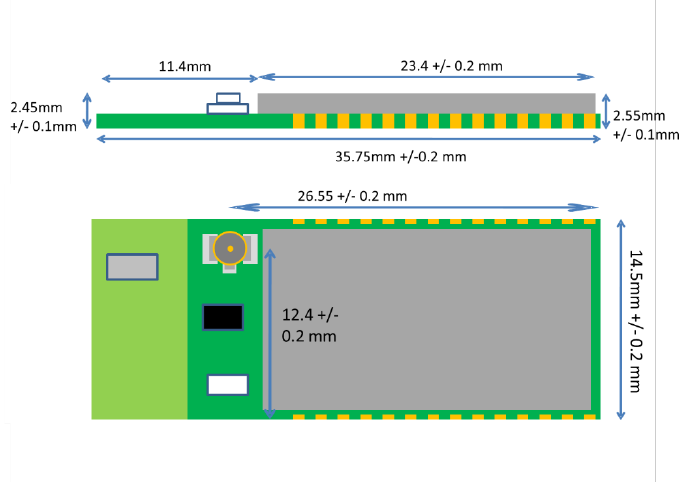
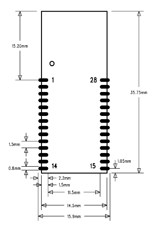
4 Physical Dimensions
Figure 10: Physical dimensions (top view)
Figure 11: Dimensions of WT11u-A
Silicon Laboratories Finland Oy
Page 20 of 51
Figure 12: Dimensions of WT11u-E
Silicon Laboratories Finland Oy
Page 21 of 51
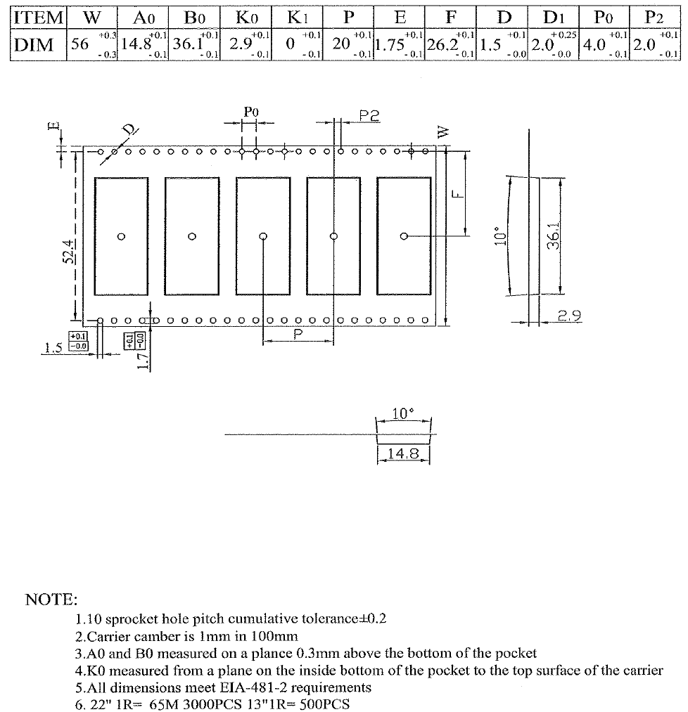
4.1 Package Drawings
Figure 13: WT11u taping
Silicon Laboratories Finland Oy
Page 22 of 51
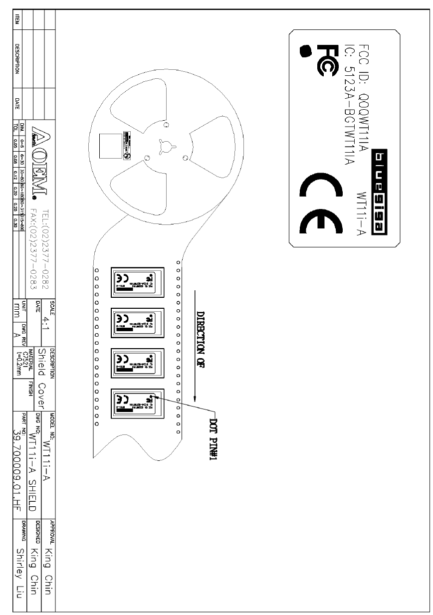
Figure 14: WT11u orientation in the reel
Silicon Laboratories Finland Oy
Page 23 of 51
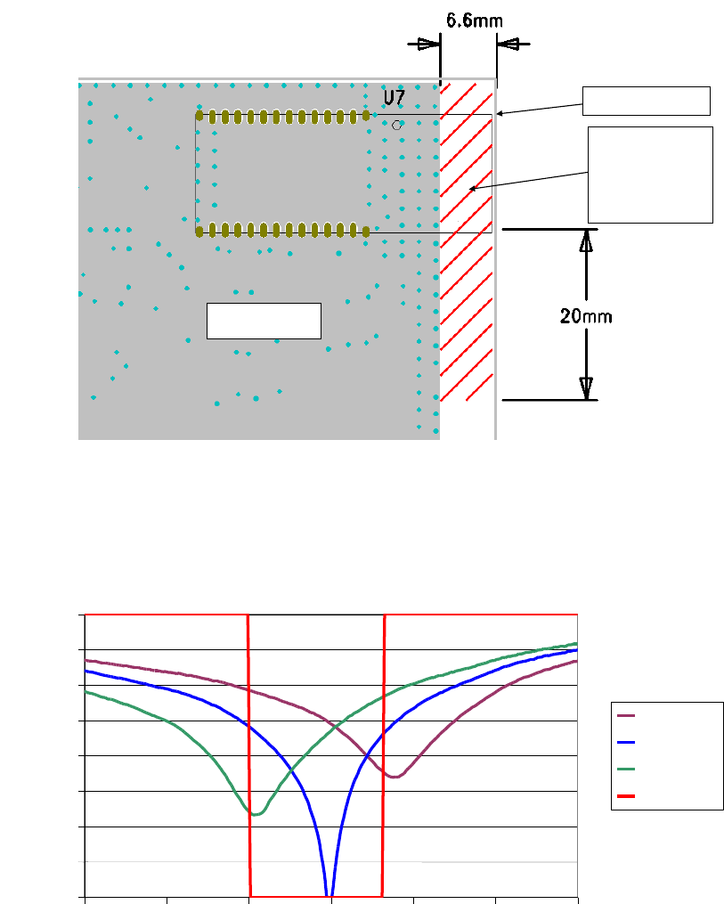
5 Layout Guidelines
WT11u is pin compatible with WT11i and WT11, despite slightly different external dimensions compared to
WT11. For a new design it recommended to follow the land pattern shown in the figure below.
Figure 15: Recommended PCB land pattern for WT11u
Do not place any copper under the antenna. The minimum recommended keep out area is shown in the Figure
16. Any dielectric material in close proximity to the antenna will effect on the impedance matching of the antenna
by lowering the resonance frequency. Figure 17 shows how different FR4 thickness under the antenna effect on
the resonance frequency. Recommended PCB thickness for the PCB is 1.6 mm – 2.8 mm. Avoid placing plastic
cover closer than 3 mm from the antenna as this will also tune the resonance frequency downwards.
Silicon Laboratories Finland Oy
Page 24 of 51
Figure 16: Recommended metal keep put area for WT11u
Figure 17: Effect of FR4 under the antenna to the resonant frequency
Use good layout practices to avoid excessive noise coupling to supply voltage traces or sensitive analog signal
traces, such as analog audio signals. If using overlapping ground planes use stitching vias separated by max 3
mm to avoid emission from the edges of the PCB. Connect all the GND pins directly to a solid GND plane and
make sure that there is a low impedance path for the return current following the signal and supply traces all
the way from start to the end.
Edge of the PCB
Do not place
copper or any
metal within
the area
marked with
cross lines
GND area with
stitching vias
Effect of PCB thickness to the antenna impedance matching
-40
-35
-30
-25
-20
-15
-10
-5
0
2300 2350 2400 2450 2500 2550 2600
Freq (MHz)
S11 (dB)
1 mm
2 mm
3 mm
BT Band
Silicon Laboratories Finland Oy
Page 25 of 51
A good practice is to dedicate one of the inner layers to a solid GND plane and one of the inner layers to supply
voltage planes and traces and route all the signals on top and bottom layers of the PCB. This arrangement will
make sure that any return current follows the forward current as close as possible and any loops are minimized.
Figure 18: Typical 4-layer PCB construction
Figure 19: Use of stitching vias to avoid emissions from the edges of the PCB
Layout
•Supply voltage
–If possible use solid power plane
–Make sure that solid GND plane follows the traces all the way
–Do not route supply voltage traces across separated GND regions so that the
path for the return current is cut
•MIC input
–Place LC filtering and DC coupling capacitors symmetrically as close to audio
pins as possible
–Place MIC biasing resistors symmetrically as close to microhone as possible.
–Make sure that the bias trace does not cross separated GND regions (DGND ->
AGND) so that the path for the return current is cut. If this is not possible the do
not separate GND regions but keep one solid GND plane.
–Keep the trace as short as possible
Signals
GND
Power
Signals
Recommended PCB layer configuration
Overlapping GND layers without
GND stitching vias Overlapping GND layers with
GND stitching vias shielding the
RF energy
Silicon Laboratories Finland Oy
Page 26 of 51
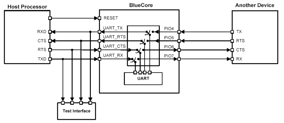
6 UART Interface
This is a standard UART interface for communicating with other serial devices.WT11u UART interface provides
a simple mechanism for communicating with other serial devices using the RS232 protocol.
Four signals are used to implement the UART function. When WT11u is connected to another digital device,
UART_RX and UART_TX transfer data between the two devices. The remaining two signals, UART_CTS and
UART_RTS, can be used to implement RS232 hardware flow control where both are active low indicators. All
UART connections are implemented using CMOS technology and have signalling levels of 0V and VDD.
UART configuration parameters, such as data rate and packet format, are set using WT11u software.
Note:
In order to communicate with the UART at its maximum data rate using a standard PC, an accelerated serial
port adapter card is required for the PC.
Parameter
Possible values
Data rate
Minimum
1200bps (2% error)
9600bps (1% error)
Maximum
3Mbps (1% error)
Flow control
RTS/CTS or None
Parity
None, Odd or Even
Number of stop bits
1 or 2
Bits per channel
8
Table 12: Possible UART Settings
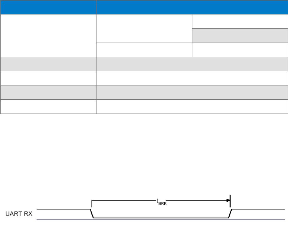
The UART interface is capable of resetting WT11u upon reception of a break signal. A break is identified by a
continuous logic low (0V) on the UART_RX terminal, as shown in Figure 20. If tBRK is longer than the value (in
microseconds), defined by PSKEY_HOST_IO_UART_RESET_TIMEOUT, (0x1a4), a reset will occur. Values
below 1000 are treated as zero and values above 255000 are truncated to 255000. This feature allows a host
to initialise the system to a known state. Also, WT11u can emit a break character that may be used to wake the
host.
Figure 20: Break Signal
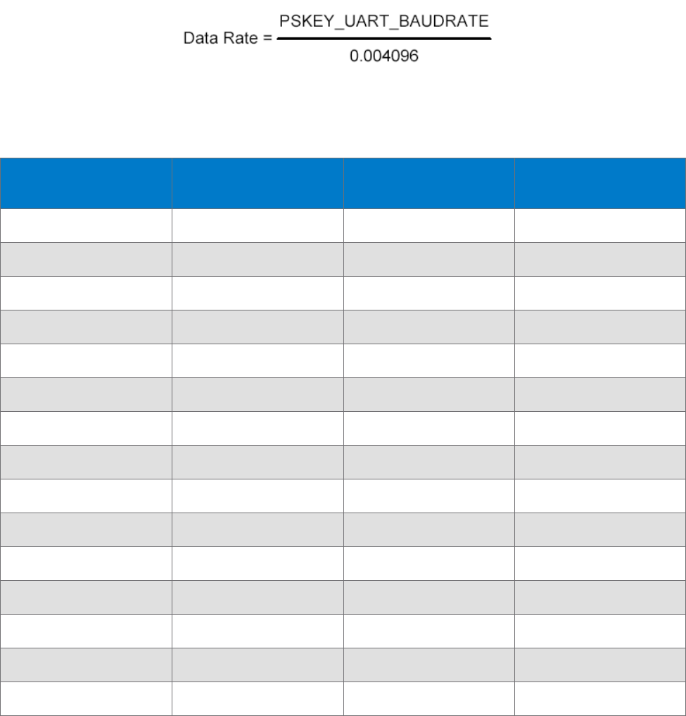
Table 13 shows a list of commonly used data rates and their associated values for PSKEY_UART_BAUD_RATE
(0x204). There is no requirement to use these standard values. Any data rate within the supported range can
be set in the PS Key according to the formula in Equation 1
Silicon Laboratories Finland Oy
Page 27 of 51
Equation 1: Data Rate
Data rate [bits/s]
Persistent store value
(Hex)
Error [bits/s]
Error [%]
1200
0x0005
5
1.73
2400
0x000A
10
1.73
4800
0x0014
20
1.73
9600
0x0027
39
-0.82
19200
0x004F
79
0.45
38400
0x009D
157
-0.18
57600
0x00EC
236
0.03
76800
0x013B
315
0.14
115200
0x01D8
472
0.03
230400
0x03B0
944
0.03
460800
0x075F
1887
-0.02
921600
0x0EBF
3775
0
1382400
0x161E
5662
-0.01
1843200
0x1D7E
7550
0
2764800
0x2C3D
11325
0
Table 13: Standard Data Rates
Silicon Laboratories Finland Oy
Page 28 of 51
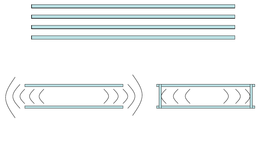
6.1 UART Bypass
Figure 21: UART Bypass Architecture
6.2 UART Configuration While Reset is Active
The UART interface for WT11u while the chip is being held in reset is tristate. This will allow the user to daisy
chain devices onto the physical UART bus. The constraint on this method is that any devices connected to this
bus must tristate when WT11u reset is de-asserted and the firmware begins to run.
6.3 UART Bypass Mode
Alternatively, for devices that do not tristate the UART bus, the UART bypass mode on the chipset can be used.
The default state of the chipset after reset is de-asserted; this is for the host UART bus to be connected to the
chipset UART, thereby allowing communication to the chipset via the UART. All UART bypass mode
connections are implemented using CMOS technology and have signalling levels of 0V and VDD.
In order to apply the UART bypass mode, a BCCMD command will be issued the chipset. Upon this issue, it will
switch the bypass to PIO[7:4] as Figure 21 indicates. Once the bypass mode has been invoked, WT11u will enter
the Deep Sleep state indefinitely.
In order to re-establish communication with WT11u, the chip must be reset so that the default configuration
takes effect.
It is important for the host to ensure a clean Bluetooth disconnection of any active links before the bypass mode
is invoked. Therefore, it is not possible to have active Bluetooth links while operating the bypass mode.
The current consumption for a device in UART bypass mode is equal to the values quoted for a device in
standby mode.
Silicon Laboratories Finland Oy
Page 29 of 51
7 USB Interface
This is a full speed (12Mbits/s) USB interface for communicating with other compatible digital devices. WT11u
acts as a USB peripheral, responding to requests from a master host controller such as a PC.
The USB interface is capable of driving a USB cable directly. No external USB transceiver is required. The
device operates as a USB peripheral, responding to requests from a master host controller such as a PC. Both
the OHCI and the UHCI standards are supported. The set of USB endpoints implemented can behave as
specified in the USB section of the Bluetooth v2.1 + EDR specification or alternatively can appear as a set of
endpoints appropriate to USB audio devices such as speakers.
As USB is a master/slave oriented system (in common with other USB peripherals), WT11u only supports USB
Slave operation.
7.1 USB Data Connections
The USB data lines emerge as pins USB_DP and USB_DN. These terminals are connected to the internal USB
I/O buffers of the chipset, therefore, have a low output impedance. To match the connection to the characteristic
impedance of the USB cable, resistors must be placed in series with USB_DP/USB_DN and the cable.
7.2 USB Pull-Up resistor
WT11u features an internal USB pull-up resistor. This pulls the USB_DP pin weakly high when WT11u is ready
to enumerate. It signals to the PC that it is a full speed (12Mbits/s) USB device.
The USB internal pull-up is implemented as a current source, and is compliant with section 7.1.5 of the USB
specification v1.2. The internal pull-up pulls USB_DP high to at least 2.8V when loaded with a 15kΩ 5% pull-
down resistor (in the hub/host) when VDD_PADS = 3.1V. This presents a Thevenin resistance to the host of at
least 900Ω. Alternatively, an external 1.5kΩ pull-up resistor can be placed between a PIO line and D+ on the
USB cable. The firmware must be alerted to which mode is used by setting PSKEY_USB_PIO_PULLUP
appropriately. The default setting uses the internal pull-up resistor.
7.3 USB Power Supply
The USB specification dictates that the minimum output high voltage for USB data lines is 2.8V. To safely meet
the USB specification, the voltage on the VDD supply terminal must be an absolute minimum of 3.1V. Silicon
Labs recommends 3.3V for optimal USB signal quality.
7.4 Self-Powered Mode
In self-powered mode, the circuit is powered from its own power supply and not from the VBUS (5V) line of the
USB cable. It draws only a small leakage current (below 0.5mA) from VBUS on the USB cable. This is the easier
mode for which to design, as the design is not limited by the power that can be drawn from the USB hub or root
port. However, it requires that VBUS be connected to WT11u via a resistor network (Rvb1 and Rvb2), so WT11u
can detect when VBUS is powered up. The chipset will not pull USB_DP high when VBUS is off.
Self-powered USB designs (powered from a battery or PSU) must ensure that a PIO line is allocated for USB
pullup purposes. A 1.5kΩ 5% pull-up resistor between USB_DP and the selected PIO line should be fitted to
the design. Failure to fit this resistor may result in the design failing to be USB compliant in self-powered mode.
The internal pull-up in the chipset is only suitable for bus-powered USB devices, e.g., dongles.
Silicon Laboratories Finland Oy
Page 30 of 51
Figure 22: USB Connections for Self-Powered Mode
The terminal marked USB_ON can be any free PIO pin. The PIO pin selected must be registered by setting
PSKEY_USB_PIO_VBUS to the corresponding pin number.
Identifier
Value
Function
Rs
0-10Ω as needed by the design **
Impedance matching to USB
cable
Rvb1
22kΩ 5%
VBUS ON sense divider
Rvb2
47kΩ 5%
VBUS ON sense divider
Figure 23: USB Interface Component Values
**) WT11u has internal 22 ohm series resistors at the USB lines.
7.5 Bus-Powered Mode
In bus-powered mode, the application circuit draws its current from the 5V VBUS supply on the USB cable.
WT11u negotiates with the PC during the USB enumeration stage about how much current it is allowed to
consume. On power-up the device must not draw more than 100 mA but after being configured it can draw up
to 500 mA.
For WT11u, the USB power descriptor should be altered to reflect the amount of power required. This is
accomplished by setting PSKEY_USB_MAX_POWER (0x2c6). This is higher than for a Class 2 application due
to the extra current drawn by the Transmit RF PA. By default for WT11u the setting is 300 mA.
When selecting a regulator, be aware that VBUS may go as low as 4.4V. The inrush current (when charging
reservoir and supply decoupling capacitors) is limited by the USB specification. See the USB Specification.
Some applications may require soft start circuitry to limit inrush current if more than 10uF is present between
VBUS and GND. The 5V VBUS line emerging from a PC is often electrically noisy. As well as regulation down
to 3.3V and 1.8V, applications should include careful filtering of the 5V line to attenuate noise that is above the
voltage regulator bandwidth. Excessive noise on WT11u supply pins will result in reduced receiver sensitivity
and a distorted RF transmit signal.
Silicon Laboratories Finland Oy
Page 31 of 51
Figure 24: USB Connections for Bus-Powered Mode
7.6 USB Suspend Current
All USB devices must permit the USB controller to place them in a USB suspend mode. While in USB Suspend,
bus-powered devices must not draw more than 2.5mA from USB VBUS (self-powered devices may draw more
than 2.5mA from their own supply). This current draw requirement prevents operation of the radio by bus-
powered devices during USB Suspend.
When computing suspend current, the current from VBUS through the bus pull-up and pull-down resistors must
be included. The pull-up resistor at the device is 1.5kΩ. (nominal). The pull-down resistor at the hub is 14.25kΩ.
to 24.80kΩ. The pull-up voltage is nominally 3.3V, which means that holding one of the signal lines high takes
approximately 200uA, leaving only 2.3mA available from a 2.5mA budget. Ensure that external LEDs and/or
amplifiers can be turned off by the chipset. The entire circuit must be able to enter the suspend mode.
7.7 USB Detach and Wake-Up Signaling
WT11u can provide out-of-band signaling to a host controller by using the control lines called USB_DETACH
and USB_WAKE_UP. These are outside the USB specification (no wires exist for them inside the USB cable),
but can be useful when embedding WT11u into a circuit where no external USB is visible to the user. Both
control lines are shared with PIO pins and can be assigned to any PIO pin by setting
PSKEY_USB_PIO_DETACH and PSKEY_USB_PIO_WAKEUP to the selected PIO number.
USB_DETACH is an input which, when asserted high, causes WT11u to put USB_DN and USB_DP in high
impedance state and turns off the pull-up resistor on DP. This detaches the device from the bus and is logically
equivalent to unplugging the device. When USB_DETACH is taken low, WT11u will connect back to USB and
await enumeration by the USB host.
USB_WAKE_UP is an active high output (used only when USB_DETACH is active) to wake up the host and
allow USB communication to recommence. It replaces the function of the software USB WAKE_UP message
(which runs over the USB cable) and cannot be sent while chipset is effectively disconnected from the bus.
Silicon Laboratories Finland Oy
Page 32 of 51
Figure 25: USB_Detach and USB_Wake_Up Signals
7.8 USB Driver
A USB Bluetooth device driver is required to provide a software interface between the chipset and the Bluetooth
software running on the host computer.
7.9 USB v2.0 Compliance and Compatibility
Although WT11u meets the USB specification, Silicon Labs cannot guarantee that an application circuit
designed around the module is USB compliant. The choice of application circuit, component choice and PCB
layout all affect USB signal quality and electrical characteristics. The information in this document is intended
as a guide and should be read in association with the USB specification, with particular attention being given to
Chapter 7. Independent USB qualification must be sought before an application is deemed USB compliant and
can bear the USB logo. Such qualification can be obtained from a USB plugfest or from an independent USB
test house.
Terminals USB_DP and USB_DN adhere to the USB Specification v2.0 (Chapter 7) electrical requirements.
The chipset is compatible with USB v2.0 host controllers; under these circumstances the two ends agree the
mutually acceptable rate of 12Mbits/s according to the USB v2.0 specification.
Silicon Laboratories Finland Oy
Page 33 of 51
8 Serial Peripheral Interface (SPI)
The SPI port can be used for system debugging. It can also be used for programming the Flash memory and
setting the PSKEY configurations. WT11u uses 16-bit data and 16-bit address serial peripheral interface, where
transactions may occur when the internal processor is running or is stopped. SPI interface is connected using
the MOSI, MISO, CSB and CLK pins.
SPI interface cannot be used for application purposes.
Silicon Laboratories Finland Oy
Page 34 of 51
9 PCM Codec Interface
PCM is a standard method used to digitize audio (particularly voice) for transmission over digital communication
channels. Through its PCM interface, WT11u has hardware support for continual transmission and reception of
PCM data, thus reducing processor overhead for wireless headset applications. WT11u offers a bidirectional
digital audio interface that routes directly into the baseband layer of the on-chip firmware. It does not pass
through the HCI protocol layer.
Hardware on WT11u allows the data to be sent to and received from a SCO connection. Up to three SCO
connections can be supported by the PCM interface at any one time.
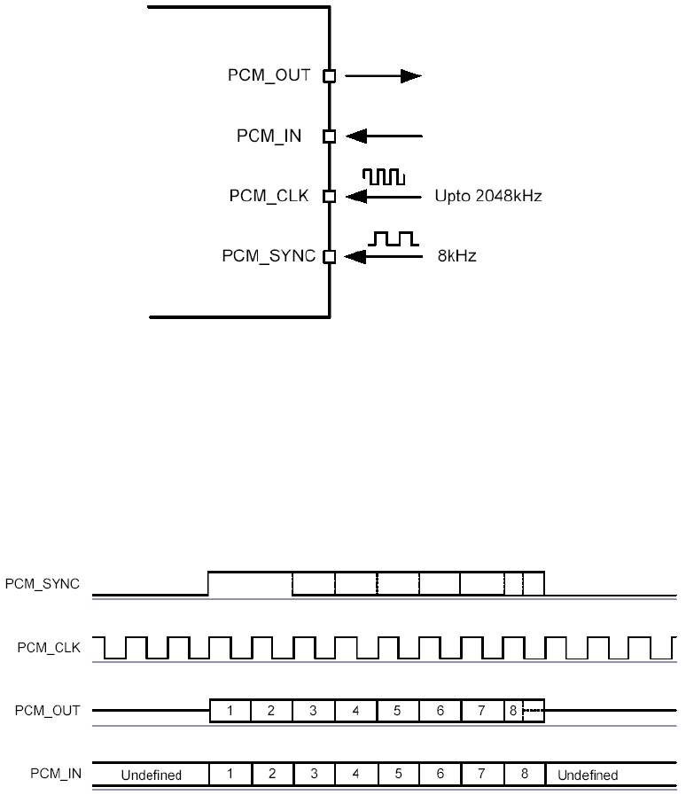
WT11u can operate as the PCM interface master generating an output clock of 128, 256 or 512kHz. When
configured as PCM interface slave, it can operate with an input clock up to 2048kHz. WT11u is compatible with
a variety of clock formats, including Long Frame Sync, Short Frame Sync and GCI timing environments.
It supports 13-bit or 16-bit linear, 8-bit µ-law or A-law companded sample formats at 8ksamples/s and can
receive and transmit on any selection of three of the first four slots following PCM_SYNC. The PCM
configuration options are enabled by setting PSKEY_PCM_CONFIG32.
WT11u interfaces directly to PCM audio devices.
NOTE: Analog audio lines are very sensitive to RF disturbance. Use good layout practices to ensure noise less
audio. Make sure that the return path for the audio signals follows the forward current all the way as close as
possible and use fully differential signals when possible. Do not compromise audio routing.
9.1 PCM Interface Master/Slave
When configured as the master of the PCM interface, WT11u generates PCM_CLK and PCM_SYNC.
Figure 26: PCM Interface Master
When configured as the Slave of the PCM interface, WT11u accepts PCM_CLK rates up to 2048kHz.
Silicon Laboratories Finland Oy
Page 35 of 51
Figure 27: PCM Interface Slave
9.2 Long Frame Sync
Long Frame Sync is the name given to a clocking format that controls the transfer of PCM data words or
samples. In Long Frame Sync, the rising edge of PCM_SYNC indicates the start of the PCM word. When WT11u
is configured as PCM master, generating PCM_SYNC and PCM_CLK, then PCM_SYNC is 8-bits long. When
WT11u is configured as PCM Slave, PCM_SYNC may be from two consecutive falling edges of PCM_CLK to
half the PCM_SYNC rate, i.e., 62.5s long.
Figure 28: Long Frame Sync (Shown with 8-bit Companded Sample)
WT11u samples PCM_IN on the falling edge of PCM_CLK and transmits PCM_OUT on the rising edge.
PCM_OUT may be configured to be high impedance on the falling edge of PCM_CLK in the LSB position or on
the rising edge.
9.3 Short Frame Sync
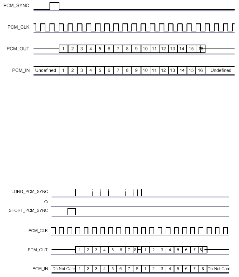
In Short Frame Sync, the falling edge of PCM_SYNC indicates the start of the PCM word. PCM_SYNC is always
one clock cycle long.
Silicon Laboratories Finland Oy
Page 36 of 51
Figure 29: Short Frame Sync (Shown with 16-bit Sample)
As with Long Frame Sync, WT11u samples PCM_IN on the falling edge of PCM_CLK and transmits PCM_OUT
on the rising edge. PCM_OUT may be configured to be high impedance on the falling edge of PCM_CLK in the
LSB position or on the rising edge.
9.4 Multi-slot Operation
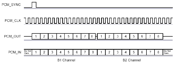
More than one SCO connection over the PCM interface is supported using multiple slots. Up to three SCO
connections can be carried over any of the first four slots.
Figure 30: Multi-slot Operation with Two Slots and 8-bit Companded Samples
9.5 GCI Interface
WT11u is compatible with the GCI, a standard synchronous 2B+D ISDN timing interface. The two 64kbits/s B
channels can be accessed when this mode is configured.
Silicon Laboratories Finland Oy
Page 37 of 51
Figure 31: GCI Interface
The start of frame is indicated by the rising edge of PCM_SYNC and runs at 8kHz. With WT11u in Slave mode,
the frequency of PCM_CLK can be up to 4.096MHz.
9.6 Slots and Sample Formats
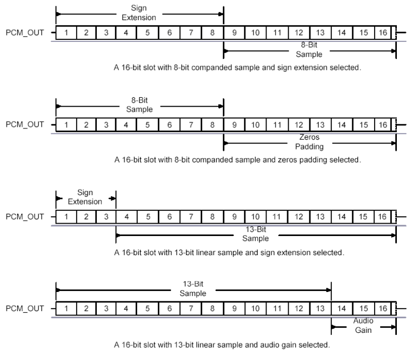
WT11u can receive and transmit on any selection of the first four slots following each sync pulse. Slot durations
can be either 8 or 16 clock cycles. Durations of 8 clock cycles may only be used with 8-bit sample formats.
Durations of 16 clocks may be used with 8-bit, 13-bit or 16-bit sample formats.
WT11u supports 13-bit linear, 16-bit linear and 8-bit -law or A-law sample formats. The sample rate is
8ksamples/s. The bit order may be little or big endian. When 16-bit slots are used, the 3 or 8 unused bits in each
slot may be filled with sign extension, padded with zeros or a programmable 3-bit audio attenuation compatible
with some Motorola codecs.
Silicon Laboratories Finland Oy
Page 38 of 51
Figure 32: 16-bit Slot Length and Sample Formats
9.7 Additional Features
WT11u has a mute facility that forces PCM_OUT to be 0. In master mode, PCM_SYNC may also be forced to
0 while keeping PCM_CLK running which some codecs use to control power down.
9.8 PCM_CLK and PCM_SYNC Generation
WT11u has two methods of generating PCM_CLK and PCM_SYNC in master mode. The first is generating
these signals by DDS from the chipset internal 4MHz clock. Using this mode limits PCM_CLK to 128, 256 or
512kHz and PCM_SYNC to 8kHz. The second is generating PCM_CLK and PCM_SYNC by DDS from an
internal 48MHz clock (which allows a greater range of frequencies to be generated with low jitter but consumes
more power). This second method is selected by setting bit 48M_PCM_CLK_GEN_EN in
PSKEY_PCM_CONFIG32. When in this mode and with long frame sync, the length of PCM_SYNC can be
either 8 or 16 cycles of PCM_CLK, determined by LONG_LENGTH_SYNC_EN in PSKEY_PCM_CONFIG32.
The Equation XXX describes PCM_CLK frequency when being generated using the internal 48MHz clock:
Silicon Laboratories Finland Oy
Page 39 of 51
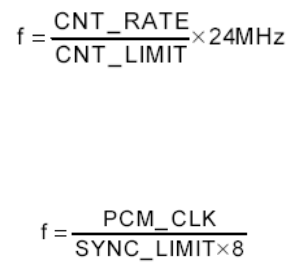
Equation 2: PCM_CLK Frequency When Being Generated Using the Internal 48MHz Clock
The frequency of PCM_SYNC relative to PCM_CLK can be set using Equation XXX:
Equation 3: PCM_SYNC Frequency Relative to PCM_CLK
CNT_RATE, CNT_LIMIT and SYNC_LIMIT are set using PSKEY_PCM_LOW_JITTER_CONFIG. As an
example, to generate PCM_CLK at 512kHz with PCM_SYNC at 8kHz, set
PSKEY_PCM_LOW_JITTER_CONFIG to 0x08080177.
9.9 PCM Configuration
The PCM configuration is set using two PS Keys, PSKEY_PCM_CONFIG32 detailed in Error! Reference
ource not found. and PSKEY_PCM_LOW_JITTER_CONFIG in Error! Reference source not found.. The
default for PSKEY_PCM_CONFIG32 is 0x00800000, i.e., first slot following sync is active, 13-bit linear voice
format, long frame sync and interface master generating 256kHz PCM_CLK from 4MHz internal clock with no
tri-state of PCM_OUT.

Silicon Laboratories Finland Oy
Page 40 of 51
Name
Bit
position
Description
-
0
Set to 0
SLAVE MODE EN
1
0 selects Master mode with internal generation of PCM_CLK and
PCM_SYNC. 1 selects Slave mode requiring externally generated
PCM_CLK and PCM_SYNC. This should be set to 1 if
48M_PCM_CLK_GEN_EN (bit 11) is set.
SHORT SYNC EN
2
0 selects long frame sync (rising edge indicates start of frame),
-
3
Set to 0
SIGN EXTENDED
EN
4
0 selects long frame sync (rising edge indicates start of frame), 1 selects
short frame sync (falling edge indicates start of frame).
LSB FIRST EN
5
0 transmits and receives voice samples MSB first, 1 uses LSB
TX TRISTATE EN
6
0 transmits and receives voice samples MSB first, 1 uses LSB
TX TRISTATE
RISING EDGE EN
7
0 tristates PCM_OUT immediately after the falling edge of PCM_CLK in
the last bit of an active slot, assuming the next slot is also not active. 1
tristates PCM_OUT after the rising edge of PCM_CLK.
SYNC SUPPRESS
EN
8
0 enables PCM_SYNC output when master, 1 suppresses PCM_SYNC
whilst keeping PCM_CLK running. Some CODECS utilize this to enter a
low power state
GCI MODE EN
9
1 enables GCI mode.
MUTE EN
10
1 forces PCM_OUT to 0.
48M PCM CLK GEN
EN
11
0 sets PCM_CLK and PCM_SYNC generation via DDS from internal 4
MHz clock. 1 sets PCM_CLK and PCM_SYNC generation via DDS from
internal 48 MHz clock.
LONG LENGTH
SYNC EN
12
0 sets PCM_SYNC length to 8 PCM_CLK cycles and 1 sets length to 16
PCM_CLK cycles. Only applies for long frame sync and with
48M_PCM_CLK_GEN_EN set to 1.
-
[20:16]
Set to 0b00000.
MASTER CLK
RATE
[22:21]
Selects 128 (0b01), 256 (0b00), 512 (0b10) kHz PCM_CLK frequency
when master and 48M_PCM_CLK_GEN_EN (bit 11) is low.
ACTIVE SLOT
[26:23]
Default is 0001. Ignored by firmaware
SAMPLE FORMAT
[28:27]
Selects between 13 (0b00), 16 (0b01), 8 (0b10) bit sample with 16 cycle
slot duration 8 (0b11) bit sample 8 cycle slot duration.
Table 14: PSKEY_PCM_CONFIG32 description

Silicon Laboratories Finland Oy
Page 41 of 51
Name
Bit position
Description
CNT LIMIT
[12:0]
Sets PCM_CLK counter limit
CNT RATE
[23:16]
Sets PCM_CLK count rate
SYNC LIMIT
[31:24]
Sets PCM_SYNC division relative to PCM_CLK
Table 15: PSKEY_PCM_LOW_JITTER_CONFIG Description
Silicon Laboratories Finland Oy
Page 42 of 51
10 I/O Parallel Ports
Six lines of programmable bidirectional input/outputs (I/O) are provided. All the PIO lines are power from VDD.
PIO lines can be configured through software to have either weak or strong pull-ups or pull-downs. All PIO lines
are configured as inputs with weak pull-downs at reset. Any of the PIO lines can be configured as interrupt
request lines or as wake-up lines from sleep modes.
WT11u has a general purpose analogue interface pin AIO[1]. This is used to access internal circuitry and control
signals. It may be configured to provide additional functionality.
Auxiliary functions available via AIO[1] include an 8-bit ADC and an 8-bit DAC. Typically the ADC is used for
battery voltage measurement. Signals selectable at this pin include the band gap reference voltage and a variety
of clock signals: 48, 24, 16, 8MHz and the XTAL clock frequency. When used with analogue signals, the voltage
range is constrained by the analogue supply voltage internally to the module (1.8V). When configured to drive
out digital level signals (e.g., clocks), the output voltage level is determined by VDD.
10.1 PIO Defaults
Silicon Labs cannot guarantee that these terminal functions remain the same. Refer to the software release
note for the implementation of these PIO lines, as they are firmware build-specific.
Silicon Laboratories Finland Oy
Page 43 of 51
11 Reset
WT11u may be reset from several sources: RESET pin, power on reset, a UART break character or via software
configured watchdog timer. The RESET pin is an active high reset and is internally filtered using the internal low
frequency clock oscillator. A reset will be performed between 1.5 and 4.0ms following RESETB being active. It
is recommended that RESET be applied for a period greater than 5ms.
The power on reset occurs when the VDD_CORE supply internally to the module falls below typically 1.5V and
is released when VDD_CORE rises above typically 1.6V. At reset the digital I/O pins are set to inputs for
bidirectional pins and outputs are tri-state.
WT11u has an internal power on reset circuit which holds the module in reset until all the supply voltages have
stabilized. The reset pin must be either floating or connected to high impedance during power on in order for
the power on reset circuit to work properly. If the reset pin is not connected to high impedance during power on,
then one must ensure that the reset is kept active until all the supply voltages have stabilized to prevent the
flash memory getting corrupted.

Silicon Laboratories Finland Oy
Page 44 of 51
11.1 Pin States on Reset
Pad name
State
PIO[7:2]
Input, weak pull-down
PCM_OUT
3-state, weak pull-down
PCM_IN
Input, weak pull-down
PCM_SYNC
Input, weak pull-down
PCM_CLK
Input, weak pull-down
UART_TX
3-state, weak pull-up
UART_RX
Input, weak pull-down
UART_RTS
3-state, weak pull-up
UART_CTS
Input, weak pull-down
USB+
Input, weak pull-down
USB-
Input, weak pull-down
SPI_CSB
Input, weak pull-down
SPI_CLK
Input, weak pull-down
SPI_MOSI
Input, weak pull-down
SPI_MISO
3-state, weak pull-down
AIO[1]
Output, driving low
Table 16: Pin States on Reset

Silicon Laboratories Finland Oy
Page 45 of 51
12 Certifications
The certifications for the WT11u are pending.
12.1 Bluetooth
The WT11u module is Bluetooth qualified and listed as a controller subsystem and it is Bluetooth compliant to
the following profiles of the core spec version 2.1/2.1+EDR.
Baseband
HCI
Link Manager
Radio
The WT11u-E radio has been tested using an external antenna with a maximum gain of 2.3 dBi and the
Bluetooth qualification is valid for any antenna with the same or less gain.
12.2 FCC
This device complies with Part 15 of the FCC Rules. Operation is subject to the following two conditions:
(1) this device may not cause harmful interference, and
(2) this device must accept any interference received, including interference that may cause undesired
operation.
Any changes or modifications not expressly approved by Bluegiga Technologies could void the user’s authority
to operate the equipment.
FCC RF Radiation Exposure Statement:
This equipment complies with FCC radiation exposure limits set forth for an uncontrolled environment. End
users must follow the specific operating instructions for satisfying RF exposure compliance. This transmitter
meets both portable and mobile limits as demonstrated in the RF Exposure Analysis. This transmitter must not
be co-located or operating in conjunction with any other antenna or transmitter except in accordance with FCC
multi-transmitter product procedures.
As long as the condition above is met, further transmitter testing will not be required. However, the OEM
integrator is still responsible for testing their end-product for any additional compliance requirements required
with this module installed (for example, digital device emissions, PC peripheral requirements, etc.).
OEM Responsibilities to comply with FCC Regulations
The WT11U Module has been certified for integration into products only by OEM integrators under the following
conditions:
The antenna(s) must be installed such that a minimum separation distance of 42 mm is maintained
between the radiator (antenna) and all persons at all times.

Silicon Laboratories Finland Oy
Page 46 of 51
The transmitter module must not be co-located or operating in conjunction with any other antenna or
transmitter except in accordance with FCC multi-transmitter product procedures.
As long as the two conditions above are met, further transmitter testing will not be required. However, the OEM
integrator is still responsible for testing their end-product for any additional compliance requirements required
with this module installed (for example, digital device emissions, PC peripheral requirements, etc.).
IMPORTANT NOTE: In the event that these conditions cannot be met (for certain configurations or co-location
with another transmitter), then the FCC authorization is no longer considered valid and the FCC ID cannot be
used on the final product. In these circumstances, the OEM integrator will be responsible for re-evaluating the
end product (including the transmitter) and obtaining a separate FCC authorization.
End Product Labeling
The WT11U module is labeled with its own FCC ID. If the FCC ID is not visible when the module is installed
inside another device, then the outside of the device into which the module is installed must also display a label
referring to the enclosed module. In that case, the final end product must be labeled in a visible area with the
following:
“Contains Transmitter Module FCC ID: QOQWT11U”
or
“Contains FCC ID: QOQWT11U
The OEM integrator has to be aware not to provide information to the end user regarding how to install or
remove this RF module or change RF related parameters in the user manual of the end product
12.3 ISEDC
This radio transmitter (IC: 5123A-WT11U) has been approved by Industry Canada to operate with the
embedded chip antenna and the antennas listed in the table 18. Other antenna types are strictly prohibited for
use with this device.
This device complies with Industry Canada’s license-exempt RSS standards. Operation is subject to the
following two conditions:
(1) This device may not cause interference; and
(2) This device must accept any interference, including interference that may cause undesired operation of the
device
RF Exposure Statement
Exception from routine SAR evaluation limits are given in RSS-102 Issue5. WT11U meets the given
requirements when the minimum separation distance to human body is less than equal to 40 mm. RF exposure
or SAR evaluation is not required when the separation distance is 40 mm or more. If the separation distance is
less than 40 mm the OEM integrator is responsible for evaluating the SAR.
OEM Responsibilities to comply with IC Regulations
The WT11U Module has been certified for integration into products only by OEM integrators under the following
conditions:
The antenna(s) must be installed such that a minimum separation distance of 40 mm is maintained
between the radiator (antenna) and all persons at all times.

Silicon Laboratories Finland Oy
Page 47 of 51
The transmitter module must not be co-located or operating in conjunction with any other antenna or
transmitter.
As long as the two conditions above are met, further transmitter testing will not be required. However, the OEM
integrator is still responsible for testing their end-product for any additional compliance requirements required
with this module installed (for example, digital device emissions, PC peripheral requirements, etc.).
IMPORTANT NOTE: In the event that these conditions cannot be met (for certain configurations or co-location
with another transmitter), then the IC authorization is no longer considered valid and the IC ID cannot be used
on the final product. In these circumstances, the OEM integrator will be responsible for re-evaluating the end
product (including the transmitter) and obtaining a separate IC authorization
End Product Labeling
The WT11U module is labeled with its own IC ID. If the IC ID is not visible when the module is installed inside
another device, then the outside of the device into which the module is installed must also display a label
referring to the enclosed module. In that case, the final end product must be labeled in a visible area with the
following:
“Contains Transmitter Module IC: 5123A-WT11U”
or
“Contains IC: 5123A-WT11U
The OEM integrator has to be aware not to provide information to the end user regarding how to install or
remove this RF module or change RF related parameters in the user manual of the end product
12.3.1 IC (français)
Cet émetteur radio (IC : 5123A-WT11U) a reçu l'approbation d'Industrie Canada pour une exploitation avec
l'antenne puce incorporée. Il est strictement interdit d'utiliser d'autres types d'antenne avec cet appareil.
Le présent appareil est conforme aux CNR d’Industrie Canada applicables aux appareils radio exempts de
licence. L’exploitation est autorisée aux deux conditions suivantes :
1) l’appareil ne doit pas produire de brouillage;
2) l’utilisateur de l’appareil doit accepter tout brouillage radioélectrique subi, même si le brouillage est
susceptible d’en compromettre le fonctionnement.
Déclaration relative à l'exposition aux radiofréquences (RF)
Les limites applicables à l’exemption de l’évaluation courante du DAS sont énoncées dans le CNR 102, 5e
édition. L'appareil WT11U répond aux exigences données quand la distance de séparation minimum par rapport
au corps humain est inférieure ou égale à 40 mm. L'évaluation de l'exposition aux RF ou du DAS n'est pas
requise quand la distance de séparation est de 40 mm ou plus. Si la distance de séparation est inférieure à
40 mm, il incombe à l'intégrateur FEO d'évaluer le DAS.
Responsabilités du FEO ayant trait à la conformité avec les règlements IC
Le module WT11U a été certifié pour une intégration dans des produits uniquement par les intégrateurs FEO
dans les conditions suivantes :
La ou les antennes doivent être installées de telle façon qu'une distance de séparation minimum de
40 mm soit maintenue entre le radiateur (antenne) et toute personne à tout moment.
Silicon Laboratories Finland Oy
Page 48 of 51
Le module émetteur ne doit pas être installé au même endroit ou fonctionner conjointement avec toute
autre antenne ou émetteur.
Dès lors que les deux conditions ci-dessus sont respectées, d'autres tests de l'émetteur ne sont pas
obligatoires. Cependant, il incombe toujours à l'intégrateur FEO de tester la conformité de son produit final vis-
à-vis de toute exigence supplémentaire avec ce module installé (par exemple, émissions de dispositifs
numériques, exigences relatives aux matériels périphériques PC, etc).
REMARQUE IMPORTANTE : S'il s'avère que ces conditions ne peuvent être respectées (pour certaines
configurations ou la colocation avec un autre émetteur), alors l'autorisation IC n'est plus considérée comme
valide et l'identifiant IC ne peut plus être employé sur le produit final. Dans ces circonstances, l'intégrateur FEO
aura la responsabilité de réévaluer le produit final (y compris l'émetteur) et d'obtenir une autorisation IC distincte.
Étiquetage du produit final
L'étiquette du module WT11U porte son propre identifiant IC. Si l'identifiant IC n'est pas visible quand le module
est installé à l'intérieur d'un autre appareil, l'extérieur de l'appareil dans lequel le module est installé doit aussi
porter une étiquette faisant référence au module qu'il contient. Dans ce cas, une étiquette comportant les
informations suivantes doit être collée sur une partie visible du produit final :
« Contient le module émetteur IC : 5123A-WT11U »
ou
« Contient IC : 5123A-WT11U »
L'intégrateur FEO doit être conscient de ne pas fournir d'informations à l'utilisateur final permettant d'installer
ou de retirer ce module RF ou de changer les paramètres liés aux RF dans le mode d'emploi du produit final.
12.4 CE
The WT11u is in conformity with the essential requirements and other relevant requirements of the R&TTE
Directive (1999/5/EC) and Radio Equiment Directive (RED) . This device is compliant with the following
standards:
Safety: EN 60950
EMC: EN 301 489
Spectrum: EN 300 328
RF Exposure: EN 62479
Formal DoC is available from www.silabs.com.
12.5 MIC Japan
TBD
12.6 KCC (Korea)
TBD
Silicon Laboratories Finland Oy
Page 49 of 51
12.7 Anatel
TBD

Silicon Laboratories Finland Oy
Page 50 of 51
12.8 Qualified Antenna Types for WT11u-E
This device has been designed to operate with a standard 2.14 dBi dipole antenna. Any antenna of a different
type or with a gain higher than 2.14 dBi is strictly prohibited for use with this device. Using an antenna of a
different type or gain more than 2.14 dBi will require additional testing for FCC, CE and IC. The required antenna
impedance is 50 Ω.
Antenna type
Maximum gain
Dipole
2.14 dBi
Table 17: Qualified Antenna Types for WT11u-E
To reduce potential radio interference to other users, the antenna type and its gain should be so chosen that
the equivalent isotropically radiated power (EIRP) is not more than that permitted for successful communication.
Any standard 2.14 dBi dipole antenna can be used without an additional application to FCC.
12.9 Moisture Sensitivity Level (MSL)
Moisture sensitivity level (MSL) of this product is 3. For the handling instructions please refer to JEDEC J-STD-
020 and JEDEC J-STD-033.
If baking is required, devices may be baked for 12 hours at 125°C +/-5°C for high temperature device containers.
Silicon Laboratories Finland Oy
Page 51 of 51