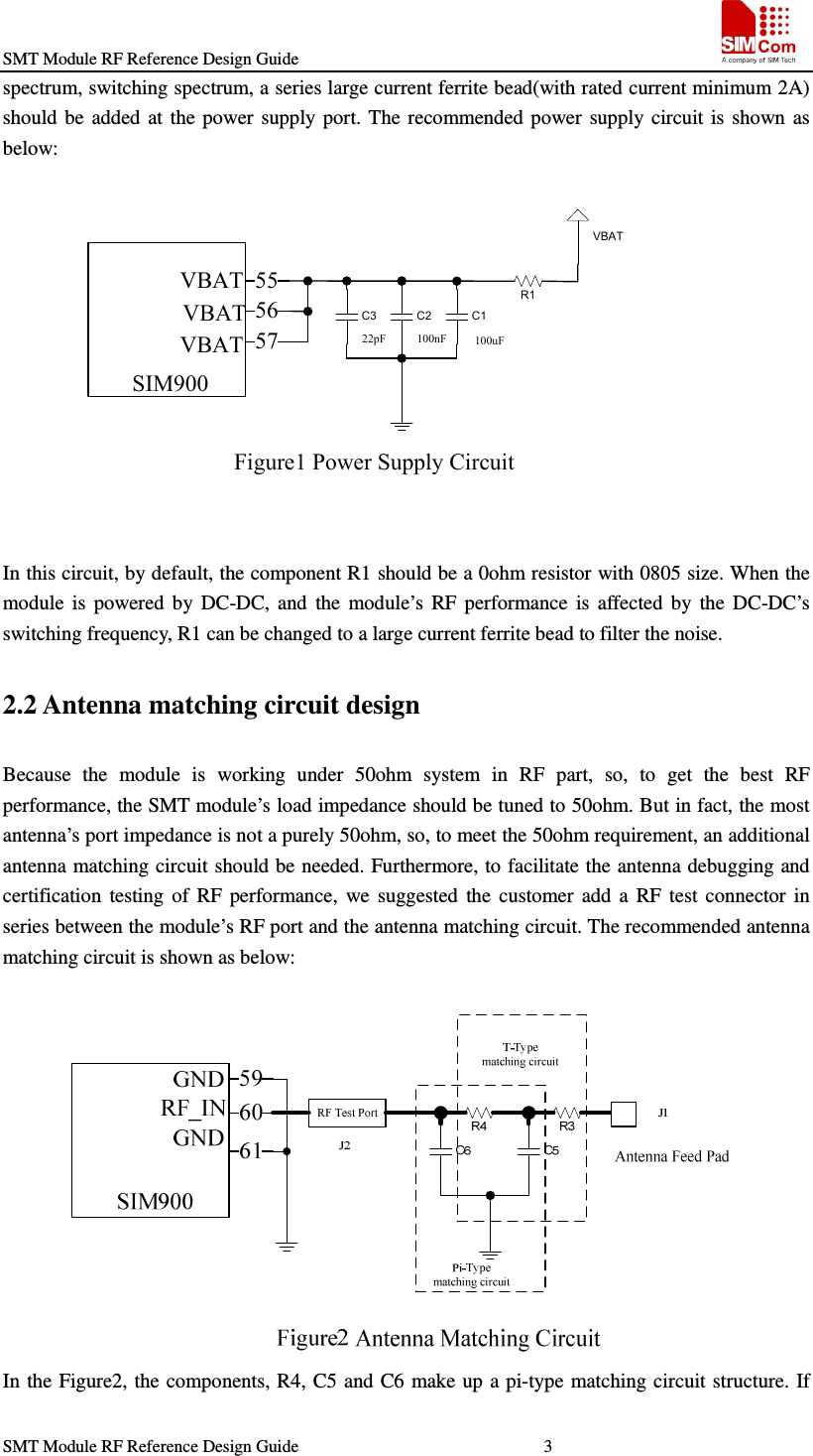
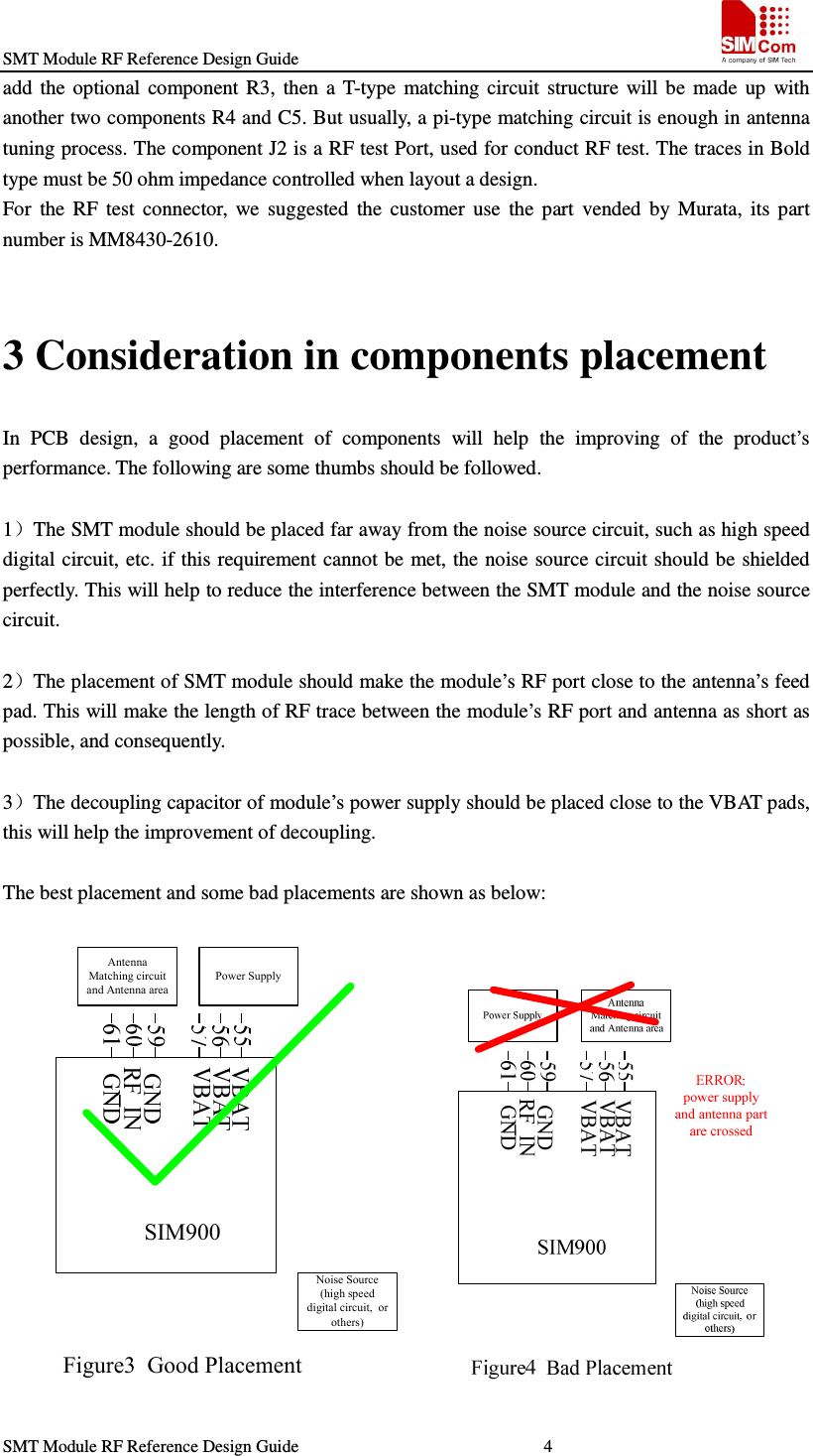
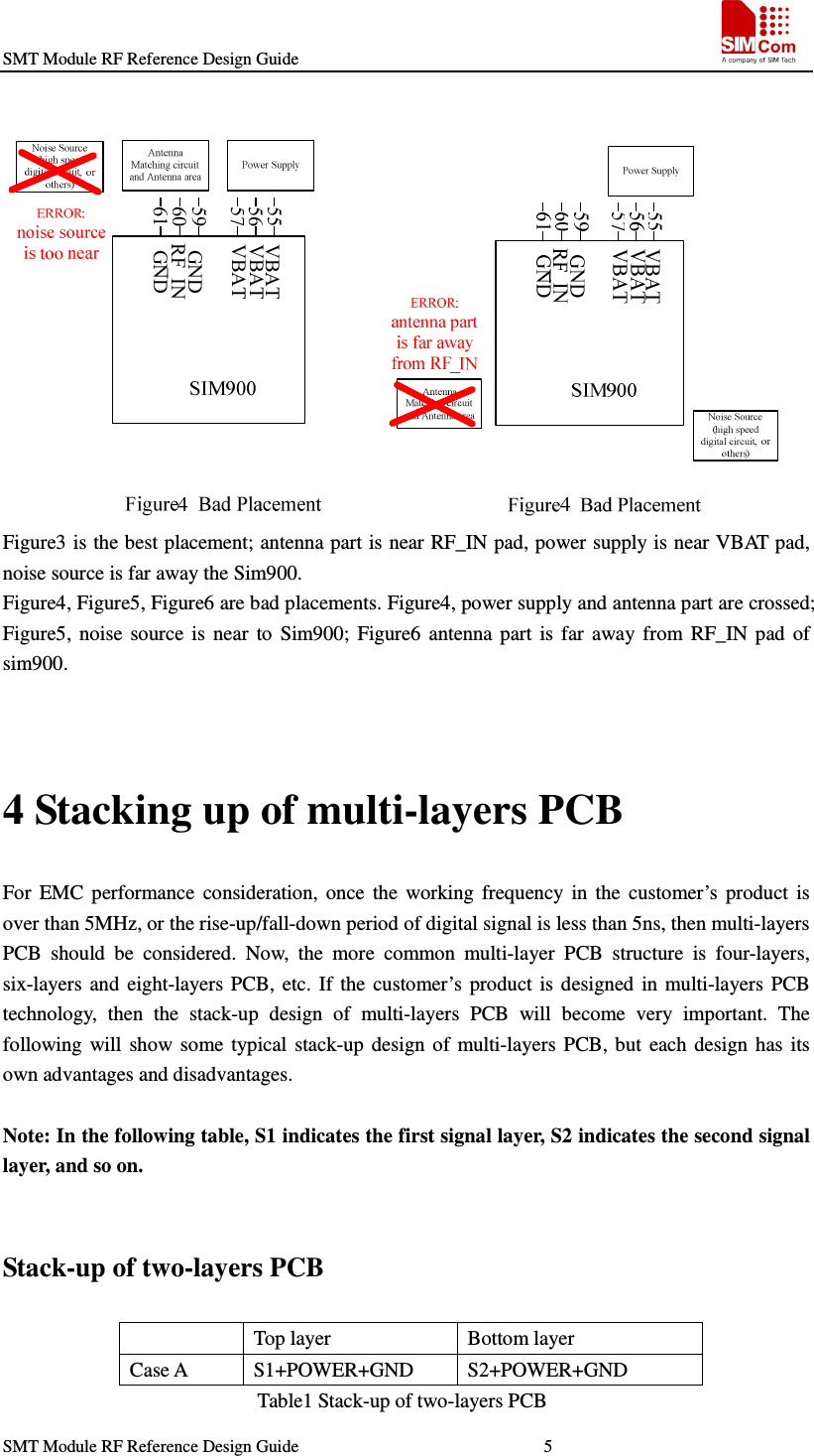
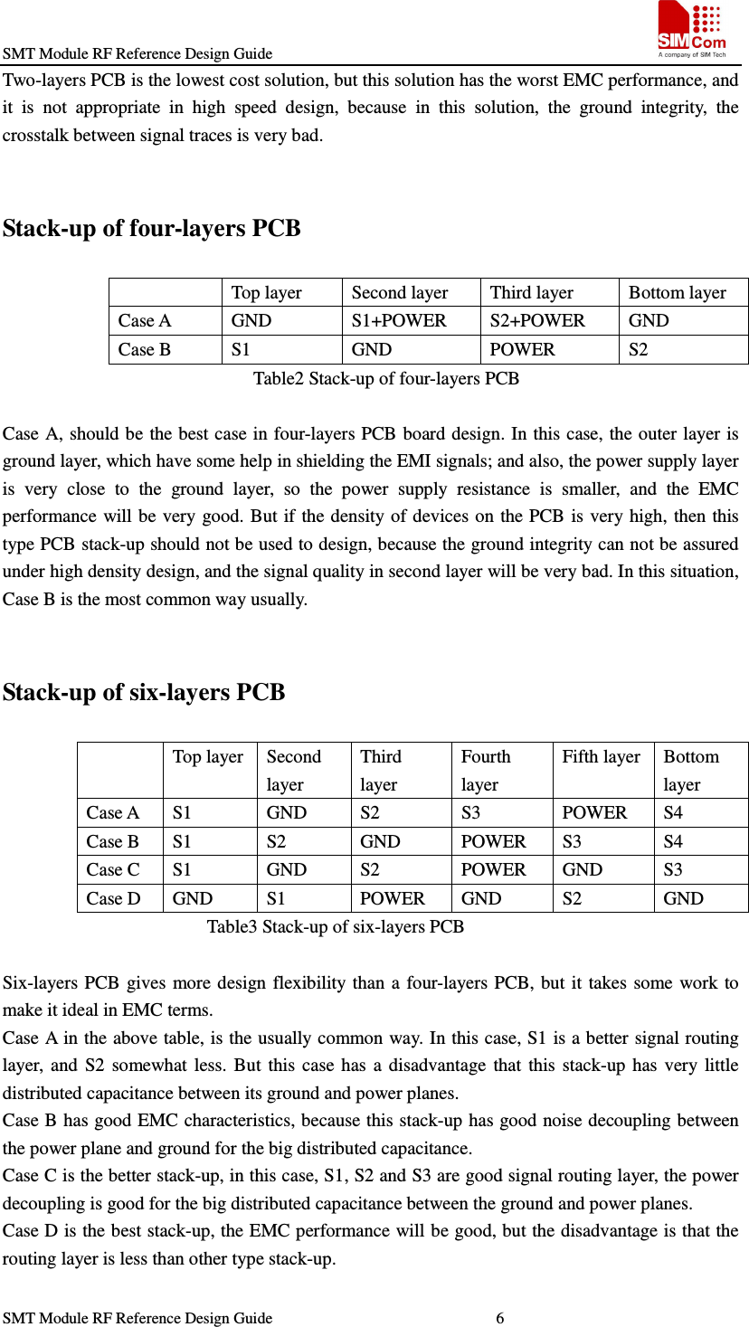
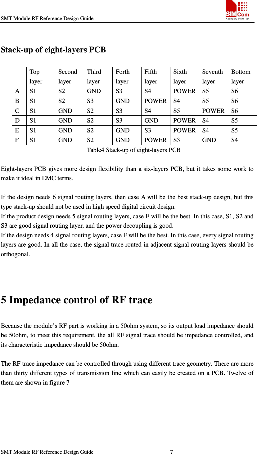
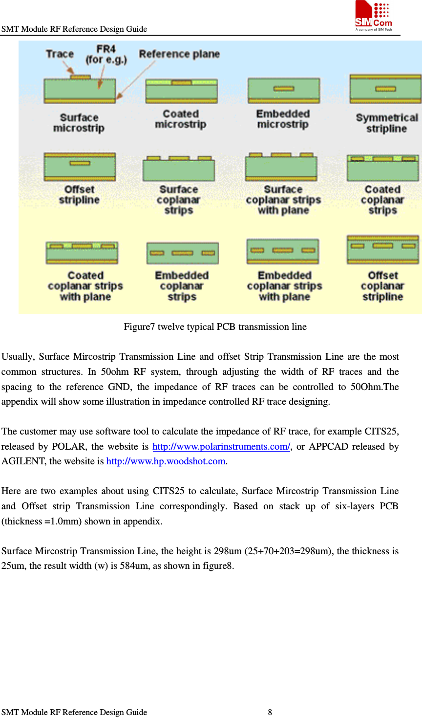
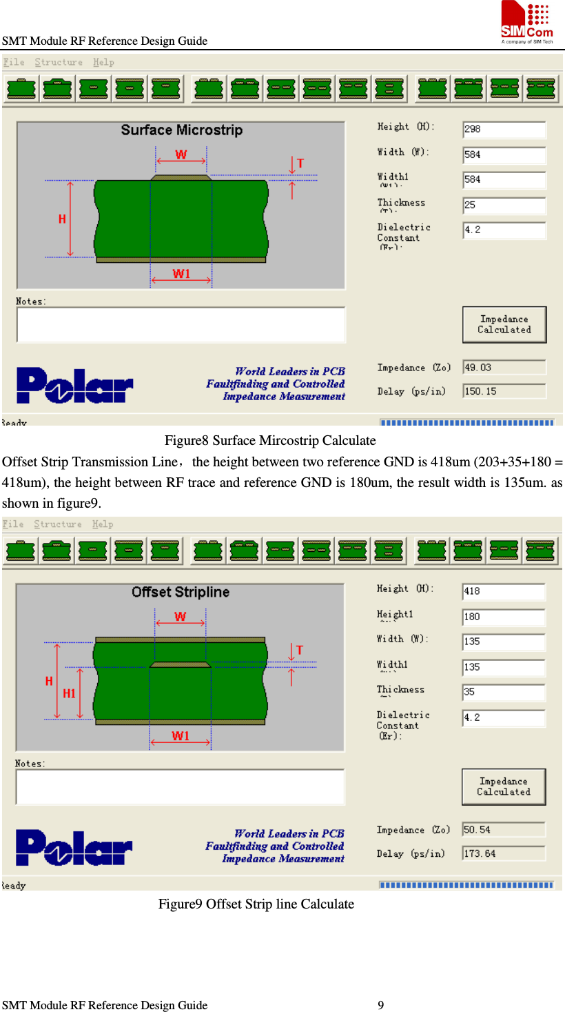
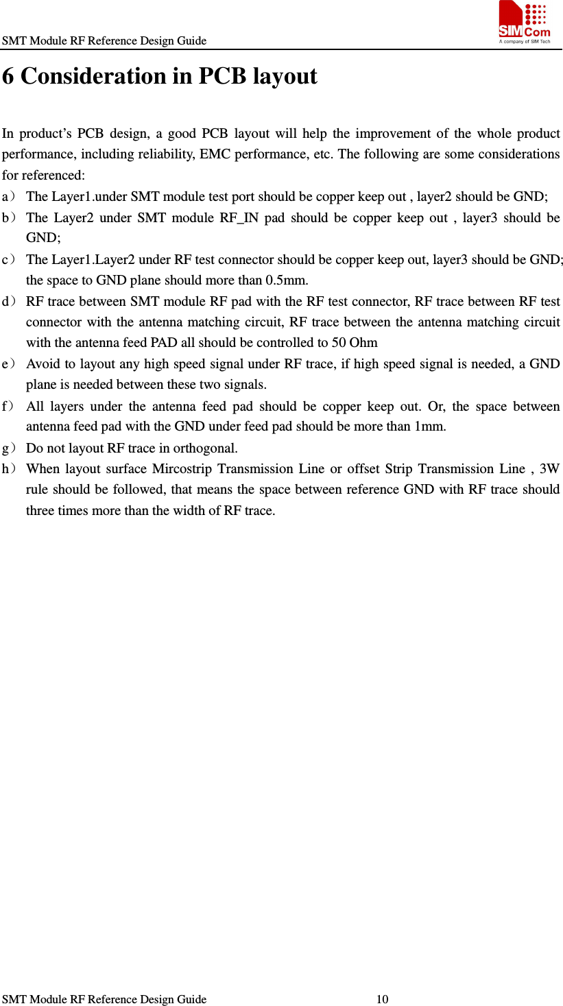
Simcom 0912142009007 Quad-band GSM/GPRS module User Manual Modular Guide

Shanghai Simcom Ltd. Quad-band GSM/GPRS module Modular Guide

Contents

Modular Guide

       SMT  Module  RF  Reference Design Guide AN_  SMT  Module  RF  Reference  Design  Guide _V1.01
 Document Title: SMT Module RF Reference Design Guide Version: 1.01 Date: 2010-1-27 Status: Release Document Control ID: AN_SMT Module RF Reference Design Guide_V1.01                    General Notes   SIMCOM offers this information as a service to its users, to support application and engineering efforts that use the products designed by SIMCOM. The information provided is based upon requirements specifically provided to SIMCOM by the users. SIMCOM has not undertaken any independent search for additional relevant information, including any information that may be in the user’s possession. Furthermore, system validation of this product designed by SIMCOM within a larger electronic system remains the responsibility of the user or the user’s system integrator. All specifications supplied herein are subject to change.      Copyright   This  document  contains  proprietary  technical  information  which  is  the  property  of  SIMCOM Limited., copying of this document and giving it to others and the using or communication of the contents thereof, are forbidden without express authority. Offenders are liable to the payment of damages. All rights reserved in the event of grant of a patent or the registration of a utility model or design. All specification supplied herein are subject to change without notice at any time.  Copyright © Shanghai SIMCOM Wireless Solutions Ltd. 2010
SMT Module RF Reference Design Guide                                                    SMT Module RF Reference Design Guide                                                        1                                                                      SMT Module RF Reference Design Guide  1 Introduction....................................................................................................................................2 2 Circuit design .................................................................................................................................2 2.1 Power supply circuit design ................................................................................................2 2.2 Antenna matching circuit design.........................................................................................3 3 Consideration in components placement........................................................................................4 4 Stacking up of multi-layers PCB....................................................................................................5 Stack-up of two-layers PCB......................................................................................................5 Stack-up of four-layers PCB .....................................................................................................6 Stack-up of six-layers PCB .......................................................................................................6 Stack-up of eight-layers PCB....................................................................................................7 5 Impedance control of RF trace.......................................................................................................7 6 Consideration in PCB layout........................................................................................................10 Appendix......................................................................................................................................... 11 Two-layers PCB ...................................................................................................................... 11 Four-layers PCB......................................................................................................................12 Six-layers PCB........................................................................................................................13 Eight-layers PCB.....................................................................................................................16             Version History Data  Version Description of change  Author 2010-1-20  01.01  Origin  Ye Haibing,   Wang Guoqiang
SMT Module RF Reference Design Guide                                                    SMT Module RF Reference Design Guide                                                        2                                                                    1 Introduction This  document  describes  the  important  points  about  RF  that  should  be  taken  into  account  in client’s application design. As SMT module can be integrated with a wide range of applications, the application notes are described in detail.    SMT  module  is  a  new  and  key  product  which  is  provided  by  SIMCom  inc.  This  type  module become very popular soon after it is released for its easy integration, good reliability. But bad RF design will lead to serious RF problems. In order to improve the RF performance, this document is formed to give the customer some design guides in RF design of SMT type module integration. Based on such considerations, at the later section, this document will describe some key issues that should be paid more attention to.  NOTE:  this  document  can apply  for  all  SMT Modules, for  example,  SIM300D,  SIM340D, SIM300W,  SIM340W,  SIM500W,  SIM540W,  SIM700D,  SIM900,  SIM900A,  SIM900D, and so on. SIM900 is selected as a demonstration in the last sections.   2 Circuit design When the customer begins to integrate the SMT type module into their product, the first thing to be  considered is  the  circuit design.  In  this  section, we will  focus  on  the  circuit design which is related to the RF  performance. This section is  divided  into  two sub-parts,  the first  is the power supply circuit design; the second is the antenna matching circuit design.  2.1 Power supply circuit design Because the SMT module is a high power consuming communication system, and the maximum working  power  will  up  to  2watt  in  worst  case,  so,  this  will  form  a  large  voltage  drop  at  the module’s power supply port. To make the SMT module have a stabilized working condition, we recommended a large tantalum capacitor (100uF or more capacity is recommended) shunted to the module’s power supply port. To get better noise decoupling performance, some additional small ceramic capacitors can be added combined with the large capacitor.    If the SMT module is powered by a DC-DC in the customer’s design, to avoid the module’s RF performance  is  affected  by  the  switching  frequency  of  the  DC-DC,  for  example,  modulation
SMT Module RF Reference Design Guide                                                    SMT Module RF Reference Design Guide                                                        3                                                                   spectrum, switching spectrum, a series large current ferrite bead(with rated current minimum 2A) should be  added  at  the  power  supply  port. The  recommended power  supply  circuit is  shown  as below:  R1C355SIM90056VBATVBAT C2 C1VBAT22pF 100nF 100uFFigure1 Power Supply CircuitVBAT 57   In this circuit, by default, the component R1 should be a 0ohm resistor with 0805 size. When the module  is  powered  by  DC-DC,  and  the  module’s  RF  performance  is  affected  by  the  DC-DC’s switching frequency, R1 can be changed to a large current ferrite bead to filter the noise. 2.2 Antenna matching circuit design   Because  the  module  is  working  under  50ohm  system  in  RF  part,  so,  to  get  the  best  RF performance, the SMT module’s load impedance should be tuned to 50ohm. But in fact, the most antenna’s port impedance is not a purely 50ohm, so, to meet the 50ohm requirement, an additional antenna matching circuit should be needed. Furthermore, to facilitate the antenna debugging and certification  testing  of  RF  performance,  we  suggested  the  customer  add  a  RF  test  connector  in series between the module’s RF port and the antenna matching circuit. The recommended antenna matching circuit is shown as below:         In the Figure2, the components, R4, C5 and C6 make up  a pi-type matching circuit structure. If
SMT Module RF Reference Design Guide                                                    SMT Module RF Reference Design Guide                                                        4                                                                   add  the  optional  component  R3,  then  a  T-type  matching  circuit  structure  will  be  made  up  with another two components R4 and C5. But usually, a pi-type matching circuit is enough in antenna tuning process. The component J2 is a RF test Port, used for conduct RF test. The traces in Bold type must be 50 ohm impedance controlled when layout a design. For  the  RF  test  connector,  we  suggested  the  customer  use  the  part  vended  by  Murata,  its  part number is MM8430-2610.  3 Consideration in components placement In  PCB  design,  a  good  placement  of  components  will  help  the  improving  of  the  product’s performance. The following are some thumbs should be followed.  1)The SMT module should be placed far away from the noise source circuit, such as high speed digital circuit, etc. if this requirement cannot be met, the noise source circuit should be shielded perfectly. This will help to reduce the interference between the SMT module and the noise source circuit.  2)The placement of SMT module should make the module’s RF port close to the antenna’s feed pad. This will make the length of RF trace between the module’s RF port and antenna as short as possible, and consequently.  3)The decoupling capacitor of module’s power supply should be placed close to the VBAT pads, this will help the improvement of decoupling.  The best placement and some bad placements are shown as below:  SIM900Figure3  Good PlacementAntenna Matching circuit and Antenna areaPower Supply Noise Source (high speed digital circuit,  or others)
SMT Module RF Reference Design Guide                                                    SMT Module RF Reference Design Guide                                                        5                                                                     VBATVBATVBAT555756RF_IN60 GNDGND6159 Figure3 is the best placement; antenna part is near RF_IN pad, power supply is near VBAT pad, noise source is far away the Sim900. Figure4, Figure5, Figure6 are bad placements. Figure4, power supply and antenna part are crossed; Figure5,  noise  source  is  near  to  Sim900;  Figure6  antenna  part  is  far  away  from  RF_IN  pad  of sim900.   4 Stacking up of multi-layers PCB For  EMC  performance  consideration,  once  the  working  frequency  in  the  customer’s  product  is over than 5MHz, or the rise-up/fall-down period of digital signal is less than 5ns, then multi-layers PCB  should  be  considered.  Now,  the  more  common  multi-layer  PCB  structure  is  four-layers, six-layers  and  eight-layers  PCB,  etc.  If  the  customer’s  product  is  designed  in  multi-layers PCB technology,  then  the  stack-up  design  of  multi-layers  PCB  will  become  very  important.  The following  will  show  some  typical  stack-up  design  of  multi-layers  PCB, but  each  design  has  its own advantages and disadvantages.    Note: In the following table, S1 indicates the first signal layer, S2 indicates the second signal layer, and so on.  Stack-up of two-layers PCB   Top layer  Bottom layer Case A  S1+POWER+GND  S2+POWER+GND                                                   Table1 Stack-up of two-layers PCB
SMT Module RF Reference Design Guide                                                    SMT Module RF Reference Design Guide                                                        6                                                                   Two-layers PCB is the lowest cost solution, but this solution has the worst EMC performance, and it  is  not  appropriate  in  high  speed  design,  because  in  this  solution,  the  ground  integrity,  the crosstalk between signal traces is very bad.                                            Stack-up of four-layers PCB   Top layer  Second layer  Third layer  Bottom layer Case A  GND  S1+POWER  S2+POWER  GND Case B  S1  GND  POWER  S2                                                       Table2 Stack-up of four-layers PCB    Case A, should be the best case in four-layers PCB board design. In this case, the outer layer is ground layer, which have some help in shielding the EMI signals; and also, the power supply layer is  very  close  to  the  ground  layer,  so  the  power  supply  resistance  is  smaller,  and  the  EMC performance will be very good. But if the density of devices on the PCB  is very high, then this type PCB stack-up should not be used to design, because the ground integrity can not be assured under high density design, and the signal quality in second layer will be very bad. In this situation, Case B is the most common way usually.    Stack-up of six-layers PCB   Top layer Second layer Third layer Fourth layer Fifth layer Bottom layer Case A  S1  GND  S2  S3  POWER  S4 Case B  S1  S2  GND  POWER  S3  S4 Case C  S1  GND  S2  POWER  GND  S3 Case D  GND  S1  POWER  GND  S2  GND                                             Table3 Stack-up of six-layers PCB  Six-layers PCB gives more design  flexibility than  a  four-layers PCB, but it  takes some  work to make it ideal in EMC terms. Case A in the above table, is the usually common way. In this case, S1 is a better signal routing layer,  and  S2  somewhat  less.  But  this  case  has  a  disadvantage  that  this  stack-up  has  very  little distributed capacitance between its ground and power planes. Case B has good EMC characteristics, because this stack-up has good noise decoupling between the power plane and ground for the big distributed capacitance. Case C is the better stack-up, in this case, S1, S2 and S3 are good signal routing layer, the power decoupling is good for the big distributed capacitance between the ground and power planes.   Case D is the best stack-up, the EMC performance will be good, but the disadvantage is that the routing layer is less than other type stack-up.
SMT Module RF Reference Design Guide                                                    SMT Module RF Reference Design Guide                                                        7                                                                    Stack-up of eight-layers PCB   Top layer Second layer Third layer Forth layer Fifth layer Sixth layer Seventh layer Bottom layer A  S1  S2  GND  S3  S4  POWER S5  S6 B  S1  S2  S3  GND  POWER S4  S5  S6 C  S1  GND  S2  S3  S4  S5  POWER S6 D  S1  GND  S2  S3  GND  POWER S4  S5 E  S1  GND  S2  GND  S3  POWER S4  S5 F  S1  GND  S2  GND  POWER S3  GND  S4                                                       Table4 Stack-up of eight-layers PCB  Eight-layers PCB gives more design flexibility than a six-layers PCB, but it takes some work to make it ideal in EMC terms.  If the design needs 6 signal routing layers, then case A will be the best stack-up design, but this type stack-up should not be used in high speed digital circuit design.   If the product design needs 5 signal routing layers, case E will be the best. In this case, S1, S2 and S3 are good signal routing layer, and the power decoupling is good. If the design needs 4 signal routing layers, case F will be the best. In this case, every signal routing layers are good. In all the case, the signal trace routed in adjacent signal routing layers should be orthogonal.   5 Impedance control of RF trace Because the module’s RF part is working in a 50ohm system, so its output load impedance should be 50ohm, to meet this requirement, the all RF signal trace should be impedance controlled, and its characteristic impedance should be 50ohm.  The RF trace impedance can be controlled through using different trace geometry. There are more than thirty different types of transmission line which can easily be created on a PCB. Twelve of them are shown in figure 7
SMT Module RF Reference Design Guide                                                    SMT Module RF Reference Design Guide                                                        8                                                                    Figure7 twelve typical PCB transmission line    Usually, Surface  Mircostrip Transmission Line  and offset Strip Transmission  Line  are  the most common  structures.  In  50ohm  RF  system,  through  adjusting  the  width  of  RF  traces  and  the spacing  to  the  reference  GND,  the  impedance  of  RF  traces  can  be  controlled  to  50Ohm.The appendix will show some illustration in impedance controlled RF trace designing.  The customer may use software tool to calculate the impedance of RF trace, for example CITS25, released by  POLAR,  the  website  is  http://www.polarinstruments.com/, or  APPCAD  released by AGILENT, the website is http://www.hp.woodshot.com.  Here  are  two  examples about  using CITS25 to  calculate, Surface Mircostrip  Transmission  Line and  Offset  strip  Transmission  Line  correspondingly.  Based  on  stack  up  of  six-layers  PCB (thickness =1.0mm) shown in appendix.  Surface Mircostrip Transmission Line, the height is 298um (25+70+203=298um), the thickness is 25um, the result width (w) is 584um, as shown in figure8.
SMT Module RF Reference Design Guide                                                    SMT Module RF Reference Design Guide                                                        9                                                                                                                  Figure8 Surface Mircostrip Calculate Offset Strip Transmission Line,the height between two reference GND is 418um (203+35+180 = 418um), the height between RF trace and reference GND is 180um, the result width is 135um. as shown in figure9.                                              Figure9 Offset Strip line Calculate
SMT Module RF Reference Design Guide                                                    SMT Module RF Reference Design Guide                                                        10                                                                   6 Consideration in PCB layout In  product’s  PCB  design,  a  good  PCB  layout  will  help  the  improvement  of  the  whole  product performance, including reliability, EMC performance, etc. The following are some considerations for referenced: a) The Layer1.under SMT module test port should be copper keep out , layer2 should be GND; b) The  Layer2  under  SMT  module  RF_IN  pad  should  be  copper  keep  out  ,  layer3  should  be GND; c) The Layer1.Layer2 under RF test connector should be copper keep out, layer3 should be GND; the space to GND plane should more than 0.5mm. d) RF trace between SMT module RF pad with the RF test connector, RF trace between RF test connector with the antenna matching circuit, RF  trace between the  antenna matching circuit with the antenna feed PAD all should be controlled to 50 Ohm e) Avoid to layout any high speed signal under RF trace, if high speed signal is needed, a GND plane is needed between these two signals. f) All  layers  under  the  antenna  feed  pad  should  be  copper  keep  out.  Or,  the  space  between antenna feed pad with the GND under feed pad should be more than 1mm. g) Do not layout RF trace in orthogonal. h) When  layout  surface  Mircostrip  Transmission  Line  or  offset  Strip  Transmission  Line  ,  3W rule should be followed, that means the space between reference GND with RF trace should three times more than the width of RF trace.
SMT Module RF Reference Design Guide                                                    SMT Module RF Reference Design Guide                                                        11                                                                   Appendix The  following  are some illustration of impedance  controlled  RF trace designing. It is should  be noted that the RF trace’s width and spacing to the reference ground is combined to specific PCB stack-up(the PCB’s thickness, clearance between every layer). Two-layers PCB
SMT Module RF Reference Design Guide                                                    SMT Module RF Reference Design Guide                                                        12                                                                   Four-layers PCB
SMT Module RF Reference Design Guide                                                    SMT Module RF Reference Design Guide                                                        13                                                                   Six-layers PCB
SMT Module RF Reference Design Guide                                                    SMT Module RF Reference Design Guide                                                        14
SMT Module RF Reference Design Guide                                                    SMT Module RF Reference Design Guide                                                        15
SMT Module RF Reference Design Guide                                                    SMT Module RF Reference Design Guide                                                        16                                                                   Eight-layers PCB
SMT Module RF Reference Design Guide                                                    SMT Module RF Reference Design Guide                                                        17
SMT Module RF Reference Design Guide                                                    SMT Module RF Reference Design Guide                                                        18                                                                           Contact us: Shanghai SIMCOM Wireless Solutions Ltd Add: SIM Technology Building, No. 633, JinZhong Road, Shanghai,PRChina 200335 Tel: +86 21 32523300 Fax: +86 21 32523200 URL:www.sim.com

Navigation menu