Simcom 1009092010008 GSM/GPRS/EDGE/WCDMA/HSDPA module User Manual SIM5216A HD V1 02 100826
Shanghai Simcom Ltd. GSM/GPRS/EDGE/WCDMA/HSDPA module SIM5216A HD V1 02 100826
UserManual.wiki
>
Simcom
>
1009092010008 User Manual
Installation instructions
Navigation menu
Upload a User Manual
Namespaces
Wiki Guide
HTML
PDF
Info
Views
User Manual
Discussion / Help
Navigation
![Document Title: SIM5216A Hardware Design Version: 1.02 Date: 2010-08-26 Status: Release Document Control ID: SIM5216A _HD_V1.02 General Notes SIMCOM offers this information as a service to its customers, to support application and engineering efforts that use the products designed by SIMCOM. The information provided is based upon requirements specifically provided to SIMCOM by the customers. SIMCOM has not undertaken any independent search for additional relevant information, including any information that may be in the customer’s possession. Furthermore, system validation of this product designed by SIMCOM within a larger electronic system remains the responsibility of the customer or the customer’s system integrator. All specifications supplied herein are subject to change. NOTICE: This device complies with Part 15 of the FCC Rules [and with RSS-210 of Industry Canada]. Operation is subject to the following two conditions: (1) this device may not cause harmful interference, and (2) this device must accept any interference received, including interference that may cause undesired operation. Changes or modifications made to this equipment not expressly approved by SIMCOM may void the FCC authorization to operate this equipment. This equipment has been tested and found to comply with the limits for a Class B digital device, pursuant to Part 15 of the FCC Rules. These limits are designed to provide reasonable protection against harmful interference in a residential installation. This equipment generates, uses and can radiate radio frequency energy and, if not installed and used in accordance with the instructions, may cause harmful interference to radio communications. However, there is no guarantee that interference will not occur in a particular installation. If this equipment does cause harmful interference to radio or television reception, which can be determined by turning the equipment off and on, the user is encouraged to try to correct the interference by one or more of the following measures: • Reorient or relocate the receiving antenna. • Increase the separation between the equipment and receiver. • Connect the equipment into an outlet on a circuit different from that to which the receiver is connected. • Consult the dealer or an experienced radio/TV technician for help.](https://usermanual.wiki/Simcom/1009092010008/User-Guide-1371471-Page-2.png)
![SIM5216A _HD_V1.02 Hardware Design SIM5216A _HD_V1.02 26.08.2010 2This Class [B] digital apparatus complies with Canadian ICES-003. Cet appareil numérique de la classe [*] est conforme à la norme NMB-003 du Canada. Radiofrequency radiation exposure Information: This equipment complies with FCC radiation exposure limits set forth for an uncontrolled environment. This equipment should be installed and operated with minimum distance of 20 cm between the radiator and your body. This transmitter must not be co-located or operating in conjunction with any other antenna or transmitter. Copyright This document contains proprietary technical information which is the property of SIMCOM Limited., copying of this document and giving it to others and the using or communication of the contents thereof, are forbidden without express authority. Offenders are liable to the payment of damages. All rights reserved in the event of grant of a patent or the registration of a utility model or design. All specification supplied herein are subject to change without notice at any time. Copyright © Shanghai SIMCOM Wireless Solutions Ltd. 2010](https://usermanual.wiki/Simcom/1009092010008/User-Guide-1371471-Page-3.png)
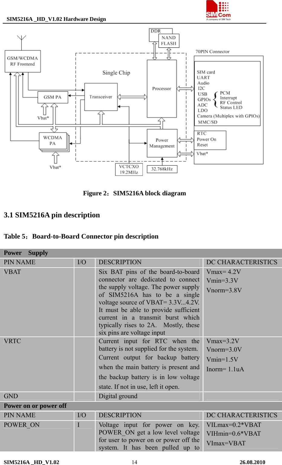
![SIM5216A _HD_V1.02 Hardware Design SIM5216A _HD_V1.02 26.08.2010 61 Introduction This document describes the hardware interface of the SIMCOM SIM5216A module that connects to the specific application and the air interface. As SIM5216A can be integrated with a wide range of applications, all functional components of SIM5216A are described in great detail. This document can help you quickly understand SIM5216A interface specifications, electrical and mechanical details. With the help of this document and other SIM5216A application notes, user guide, you can use SIM5216A module to design and set-up mobile applications quickly. 1.1 Related documents Table 1: Related documents SN Document name Remark [1] SIMCOM_SIM5216_ATC_EN_V1.03 SIMCOM_SIM5216_ATC_EN_V1.03 [2] ITU-T Draft new recommendationV.25ter: Serial asynchronous automatic dialing and control [3] GSM 07.07: Digital cellular telecommunications (Phase 2+); AT command set for GSM Mobile Equipment (ME) [4] GSM 07.10: Support GSM 07.10 multiplexing protocol [5] GSM 07.05: Digital cellular telecommunications (Phase 2+); Use of Data Terminal Equipment – Data Circuit terminating Equipment (DTE – DCE) interface for Short Message Service (SMS) and Cell Broadcast Service (CBS) [6] GSM 11.14: Digital cellular telecommunications system (Phase 2+); Specification of the SIM Application Toolkit for the Subscriber Identity Module – Mobile Equipment (SIM – ME) interface [7] GSM 11.11: Digital cellular telecommunications system (Phase 2+); Specification of the Subscriber Identity Module – Mobile Equipment (SIM – ME) interface [8] GSM 03.38: Digital cellular telecommunications system (Phase 2+); Alphabets and language-specific information [9] GSM 11.10 Digital cellular telecommunications system (Phase 2); Mobile Station (MS) conformance specification; Part 1: Conformance specification [10] 3GPP TS 51.010-1 Digital cellular telecommunications system (Release 5); Mobile Station(MS) conformance specification [11] 3GPP TS 34.124 Electromagnetic Compatibility (EMC) for mobile terminals and ancillary equipment. [12] 3GPP TS 34.121 Electromagnetic Compatibility (EMC) for mobile terminals and ancillary equipment. [13] 3GPP TS 34.123-1 Technical Specification Group Radio Access Network; Terminal conformance specification; Radio transmission and reception (FDD) [14] 3GPP TS 34.123-3 User Equipment (UE) conformance specification; Part 3: Abstract Test Suites.](https://usermanual.wiki/Simcom/1009092010008/User-Guide-1371471-Page-7.png)
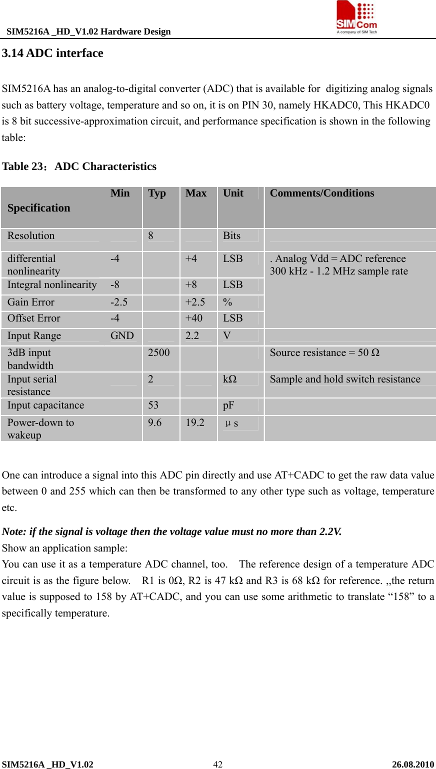
![SIM5216A _HD_V1.02 Hardware Design SIM5216A _HD_V1.02 26.08.2010 7[15] EN 301 908-02 V3.2.1 Electromagnetic compatibility and Radio spectrum Matters (ERMStations (BS) and User Equipment (UE) for IMT-2000 Third Genecellular networks; Part 2: Harmonized EN for IMT-2000, CDMA DSpread (UTRA FDD) (UE) covering essential requirements of artiof the R&TTE Directive [16] EN 301 489-24 V1.4.1 Electromagnetic compatibility and Radio Spectrum Matters (ERM); Electromagnetic Compatibility (EMC) standard for radio equipment and services; Part 24: Specific conditions for IMT-2000 CDMA Direct Spread (UTRA) for Mobile and portable (UE) radio and ancillary equipment [17] IEC/EN60950-1(2006) Safety of information technology equipment (2000) [18] 3GPP TS 51.010-1 Digital cellular telecommunications system (Release 5); Mobile Station (MS) conformance specification [19] GCF-CC V3.23.1 Global Certification Forum - Certification Criteria [20] 2002/95/EC Directive of the European Parliament and of the Council of 27 January 2003 on the restriction of the use of certain hazardous substances in electrical and electronic equipment(RoHS) [21] SIM52xx_Audio_Application_Note_V1.01 SIM52xx_Audio_Application_Note_V1.01 [22] SIM52xx_PCM_Application_Note_V1.02 SIM52xx_PCM_Application_Note_V1.02 [23] SIM52xx_Waking_up_Application_Note_V1.03 SIM52xx_Waking_up_Application_Note_V1.03 1.2 Terms and abbreviations Table 2: Terms and abbreviations Abbreviation Description ADC Analog-to-Digital Converter ARP Antenna Reference Point BER Bit Error Rate BTS Base Transceiver Station CS Coding Scheme CSD Circuit Switched Data CTS Clear to Send DAC Digital-to-Analog Converter DRX Discontinuous Reception DSP Digital Signal Processor DTE Data Terminal Equipment (typically computer, terminal, printer) DTR Data Terminal Ready DTX Discontinuous Transmission EFR Enhanced Full Rate EGSM Enhanced GSM EMC Electromagnetic Compatibility ESD Electrostatic Discharge ETS European Telecommunication Standard](https://usermanual.wiki/Simcom/1009092010008/User-Guide-1371471-Page-8.png)
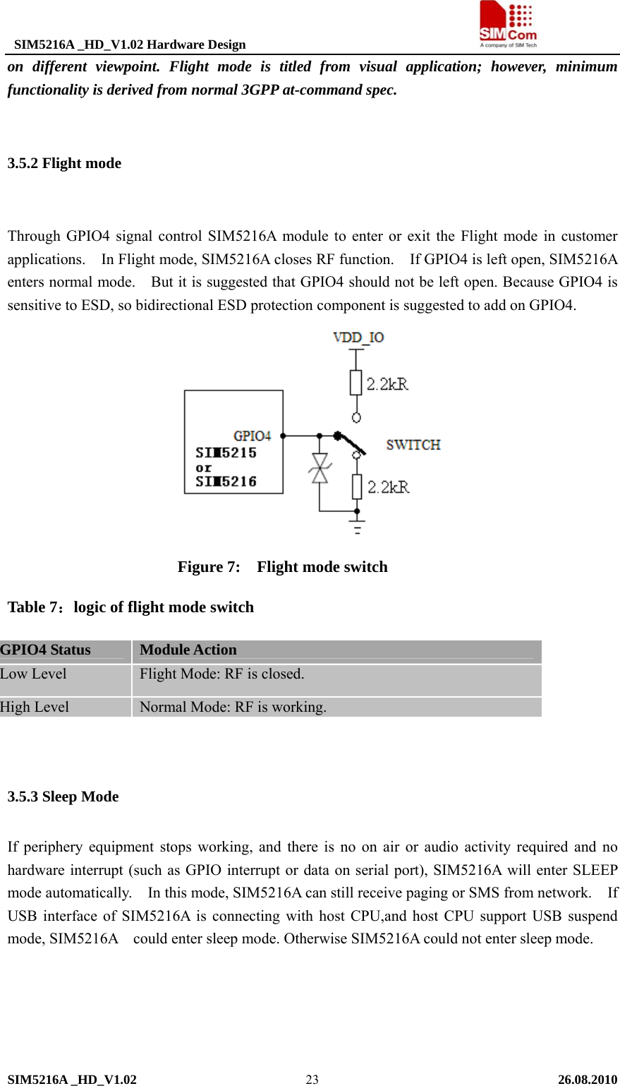
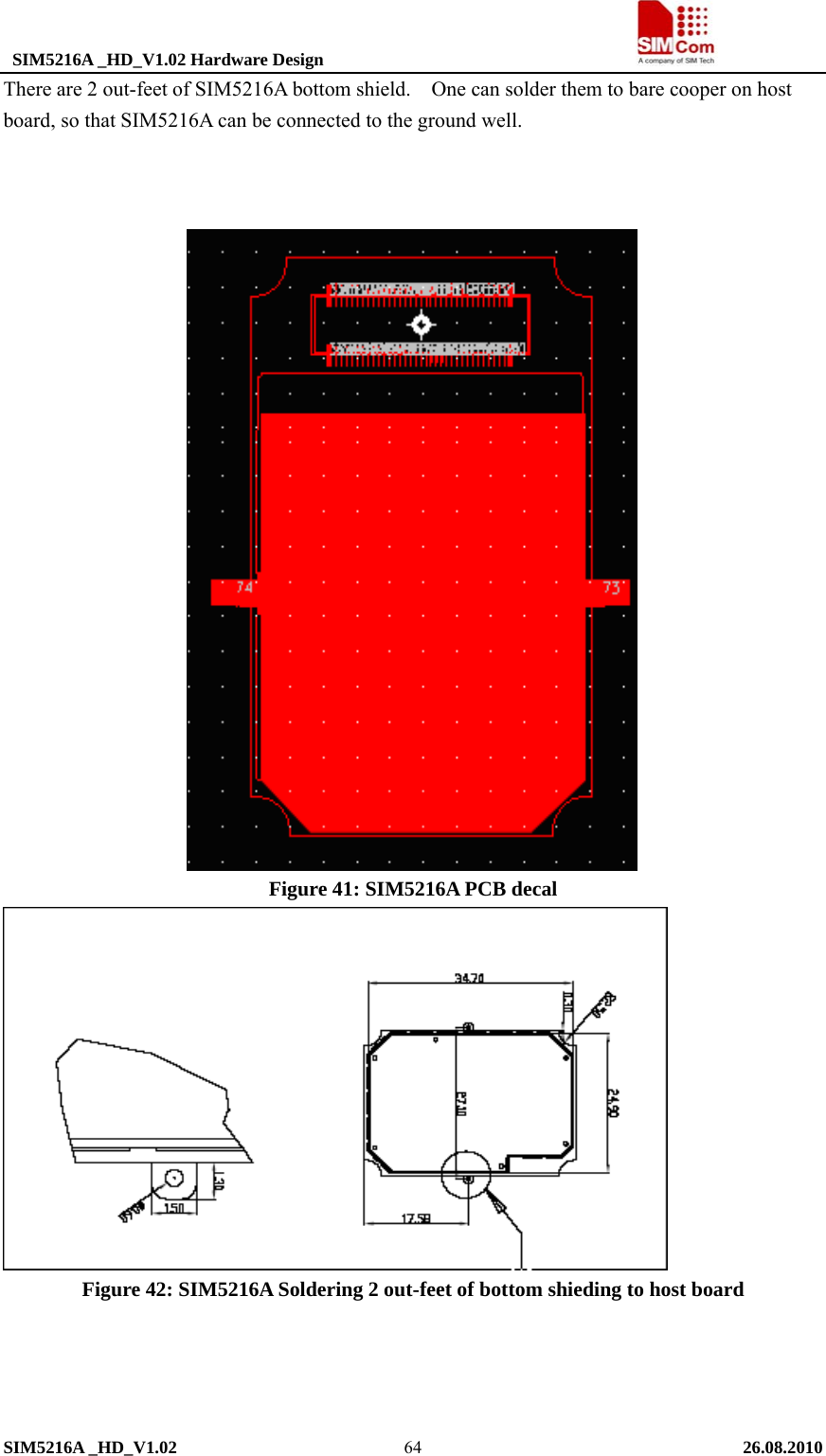
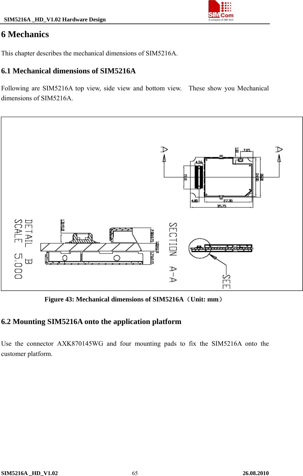
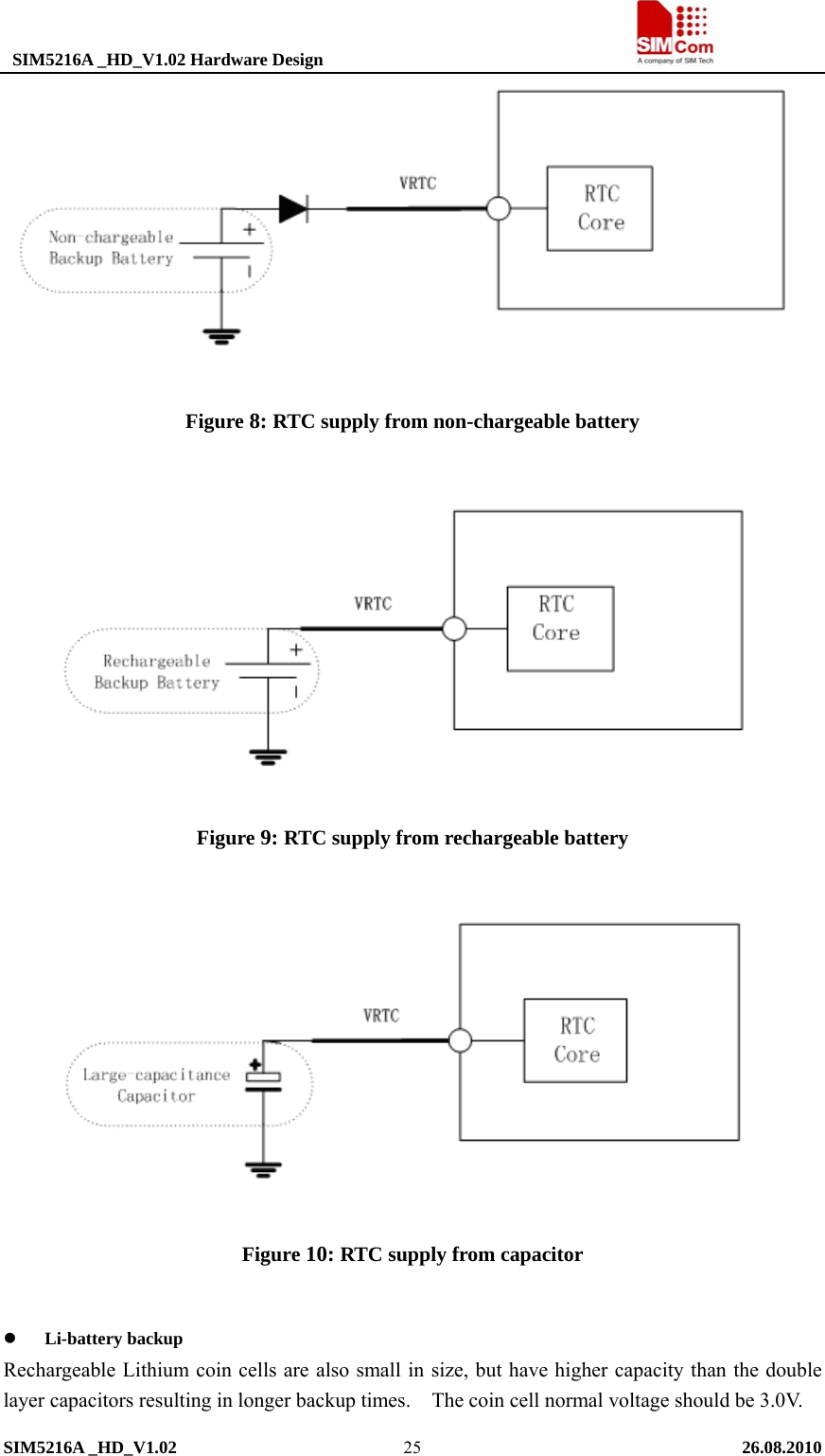
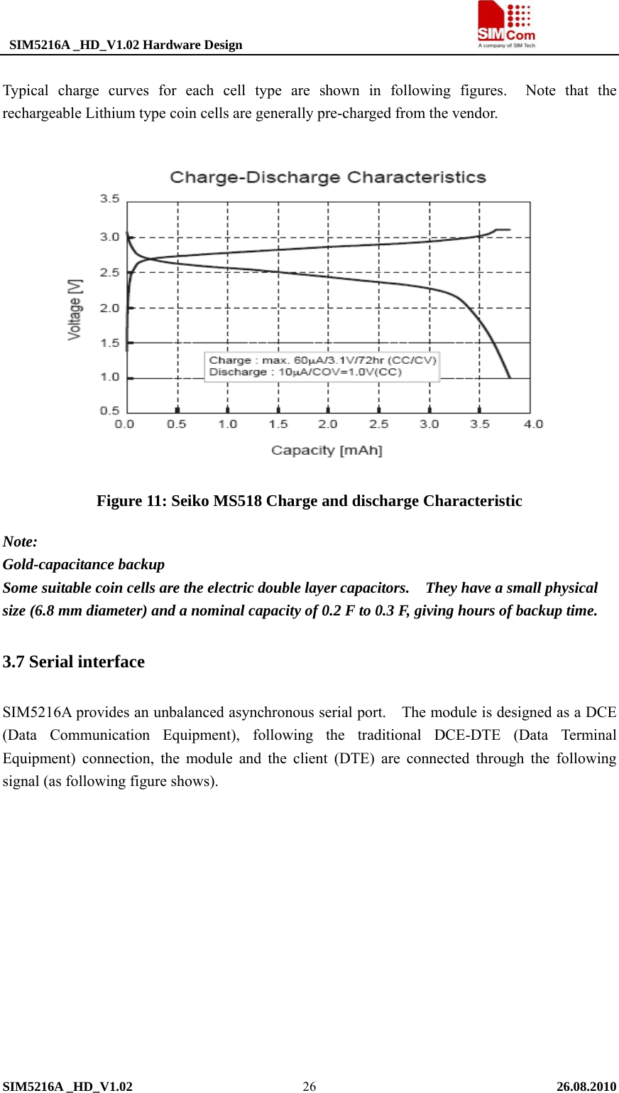
![SIM5216A _HD_V1.02 Hardware Design SIM5216A _HD_V1.02 26.08.2010 243.5.4 Wake up SIM5216A from Sleep Mode When SIM5216A is in SLEEP mode, the following method can wake up the module. z USB interface active z Receive a voice or data call from network to wake up SIM5216A. z Receive a SMS from network to wake up SIM5216A. z Receive a interrupt signal from GPIO0 z GPIO4 state change. z Receive AT command from UART. z UART DTR signal changed. Normally DTR pin will stay high but in certain condition when serial port is used in Null Modem(3-line mode). When host wants to wake up SIM5216A, it can pull down DTR for about 12ms(since SIM5216A has a debounce time of 10ms for mistaken interrupt checking). Then DTR will trigger an interrupt which will finally cause SIM5216A to be waken up from sleep mode. Note: One can enable/disable such function by AT+CDTRISRS, also One can configure the DTR’s trigger condition by AT+CDTRISRMD(only level trigger condition has debounce time). Currently the function is enabled by default and the trigger condition is low level. Please reference document [23] for detailed information of Waking_up_Application_Note. WARNING!!!: when DTR has been pulled down/up long enough to trigger the interrupt one must recover DTR to original status or the interrupt will be triggered all the time and SIM5216A may crash. 3.6 RTC backup The RTC (Real Time Clock) power supply of module can be provided by an external battery or a battery (rechargeable or non-chargeable) through the VRTC (PIN11) on the board-to-board connector. You need only a coin-cell battery or a super-cap to VRTC to backup power supply for RTC. The discharge current is smaller than 10uA. The module could update local time based on universal time and time zone from network. (This feature must be supported by the network). If this feature is used, please refer to AT command AT+CTZU and AT +CTZR. Note: The VRTC default state can be designed to a NC pin in your circuit. If you need to use the VRTC, You may connect the VRTC pin to a battery or a capacitor. The following figures show various sample circuits for RTC backup.](https://usermanual.wiki/Simcom/1009092010008/User-Guide-1371471-Page-25.png)
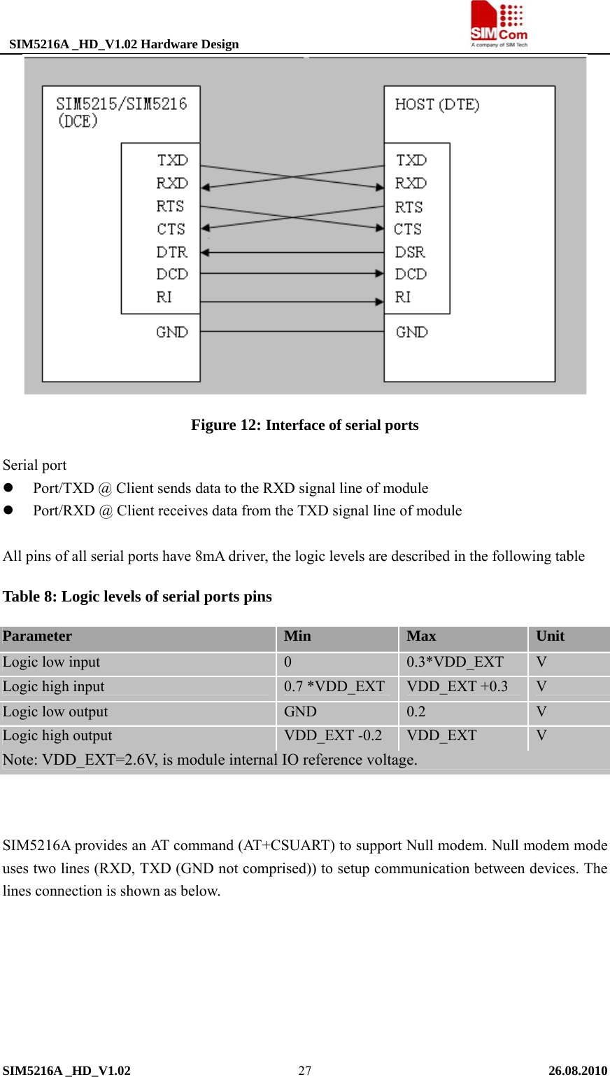
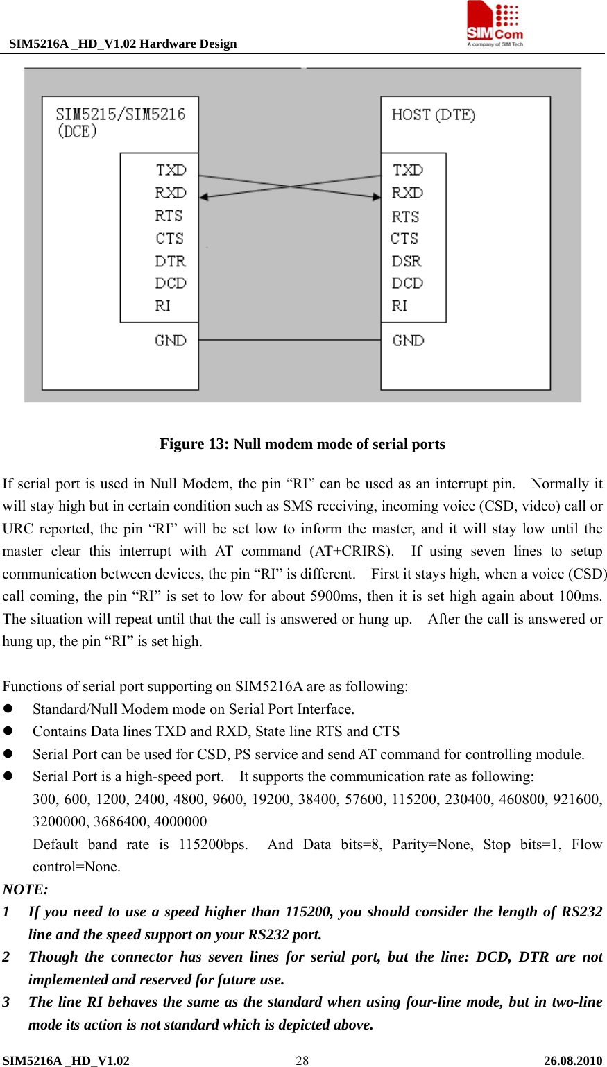
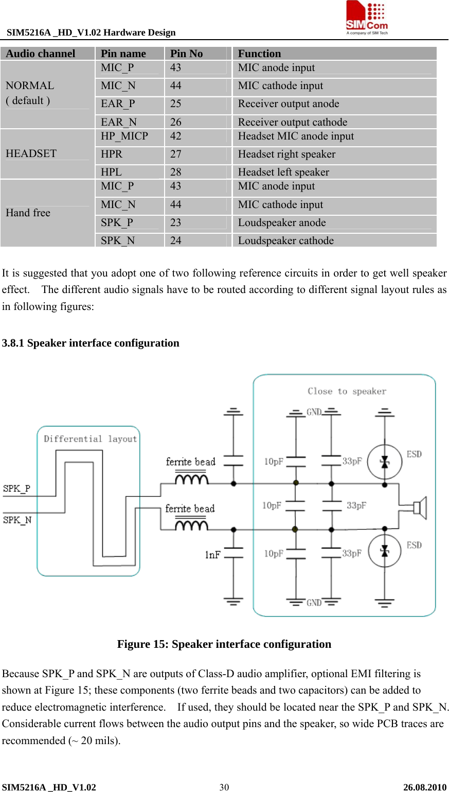
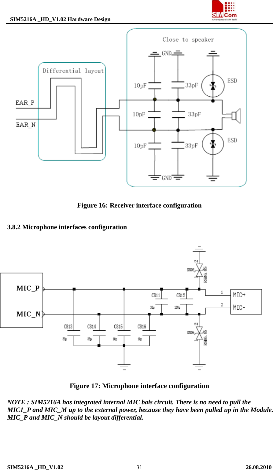
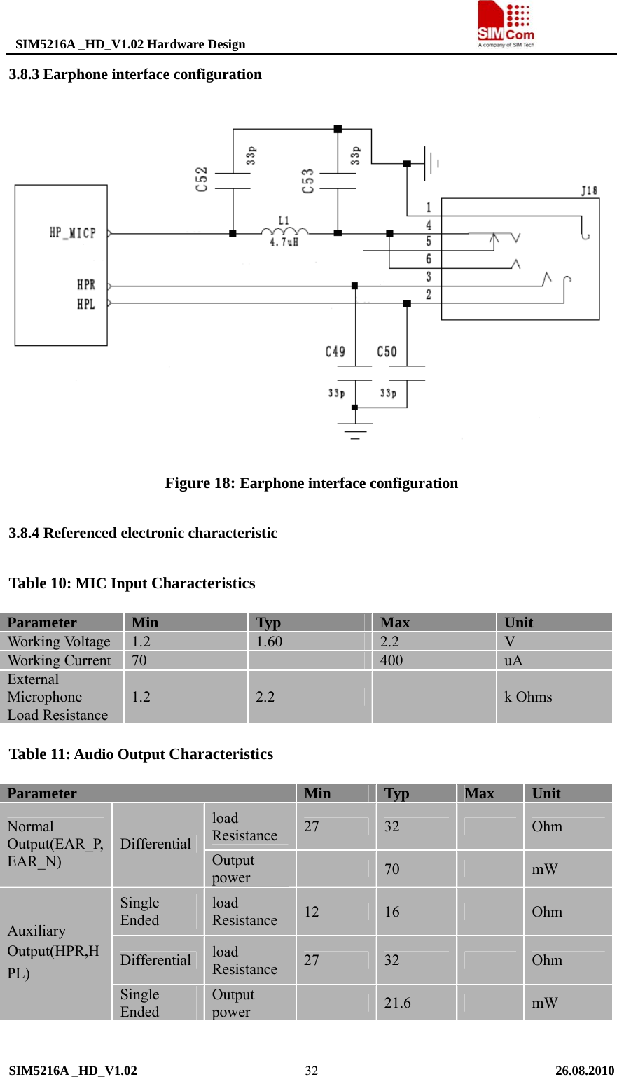
![SIM5216A _HD_V1.02 Hardware Design SIM5216A _HD_V1.02 26.08.2010 29 Default setting in HyperTerminal software is as the following figure. Figure 14: Settings of serial ports 3.8 Audio interfaces The module provides three analogy audio output channels and two analogy audio input channels. MIC_P/N and HP_MICP, are used for microphone (two analogy audio input channels), EAR_P/N, HPR/HPR and SPK_P/N are used for audio output (three analogy audio output channels). There are some AT Commands to control audio channel switch and other parameters, please refer to ATC manual. Note: Please reference document [21] for detailed information of Audio Application Note. Table 9: Audio interface signal](https://usermanual.wiki/Simcom/1009092010008/User-Guide-1371471-Page-30.png)
![SIM5216A _HD_V1.02 Hardware Design SIM5216A _HD_V1.02 26.08.2010 34parameters, 7 values calculate NOTE: if you want to better experience on audio, you should modify these parameters for your own electronic and mechanical design of audio part. The 13-tap filter parameter could be debugged and calculated by MATLAB. 3.8.5.2 Audio Programming Model The audio programming model shows how the signal path can be influenced by varying AT command parameters. Parameters <micAmp>, <txGain> , <txVol>, <txFilter>,<rxGain>, <stGain> ,<rxVol> and <rxFilter> can be adjusted with corresponding AT commands. For more information on the AT commands and parameters see Section 3.8.5.1. NOTE: Please reference document [1] for detailed information of each AT command. Figure 19: Audio programming model Note: There is no AT+CMIC in SIM5216A, because there is only one analogue hardware amplifier which is supported by AT+CMICAMP1. 3.8.5.3 Audio characteristics The electrical characteristics of the voice band part depend on the current audio mode (device number) set with the AT+CSDVC command. All values are noted for default gains. Table 14: Audio Characteristics Audio Device no. AT+CSDVC= 1 2 3 Name Handset Headset Speaker phone](https://usermanual.wiki/Simcom/1009092010008/User-Guide-1371471-Page-35.png)
![SIM5216A _HD_V1.02 Hardware Design SIM5216A _HD_V1.02 26.08.2010 35Purpose Default for DSB with Votronic handset Mono Headset handheld speaker-phoneTX-Filters Adjustable Adjustable Adjustable RX-Filters Adjustable adjusted to fit artificial ear type 3.2 low leakageAdjustable Adjustable 500 Hz HP Gain setting: Adjustable Adjustable Adjustable micAmp1 0(0 dB) 0(0 dB) 0(0 dB) txGain 23143 51811 32690 txVol 16384 16384 16384 Default MIC path Parameters txFilter [tap0~6] 0xff33, 0x05d8, 0xf488, 0x0af3, 0x24bb, 0xca42, 0x7c95 0,0,0, 0,0,0,0 0xfff3, 0x001d, 0xffb9, 0x016b, 0xfa71, 0x0c08, 0x309a rxGain 11599 6523 41155 rxVol -100 -100 0 stGain 2304 1024 0 Default Output path Parameters rxFilter [tap0~6] 0xff00, 0xfac9, 0x0571, 0xf365, 0x0bc2, 0xf2bb, 0x533a 0,0,0, 0,0,0,0 0xfd3f, 0xfc4f, 0xfb60, 0xfa27, 0xf97c, 0xf920, 0x3934 Power supply VMIC ON during call ON during call ON during call Sidetone Adjustable Adjustable Adjustable Volume control Adjustable Adjustable Adjustable Echo canceller Filter length Behaviour optimized for ON 16ms low echo ON 16ms moderate echo ON 64ms high echo Non Linear Processor with Comfort Noise Generator ON ON ON Noise Reduction -12dB -12dB -12dB MIC input signal for 0dBm0, 1 f = 1024 Hz 17.5mV 5mV 5mV EP output signal in mV rms. @ 0dBm0, 1024 Hz, no load (default gain) / @ 3.14 dBm0 508mV 2.1Vpp 407mV 1.68Vpp 1220mV 4.5Vpp Sidetone gain at default settings 25.0dB 25.3 dB -∞ dB](https://usermanual.wiki/Simcom/1009092010008/User-Guide-1371471-Page-36.png)
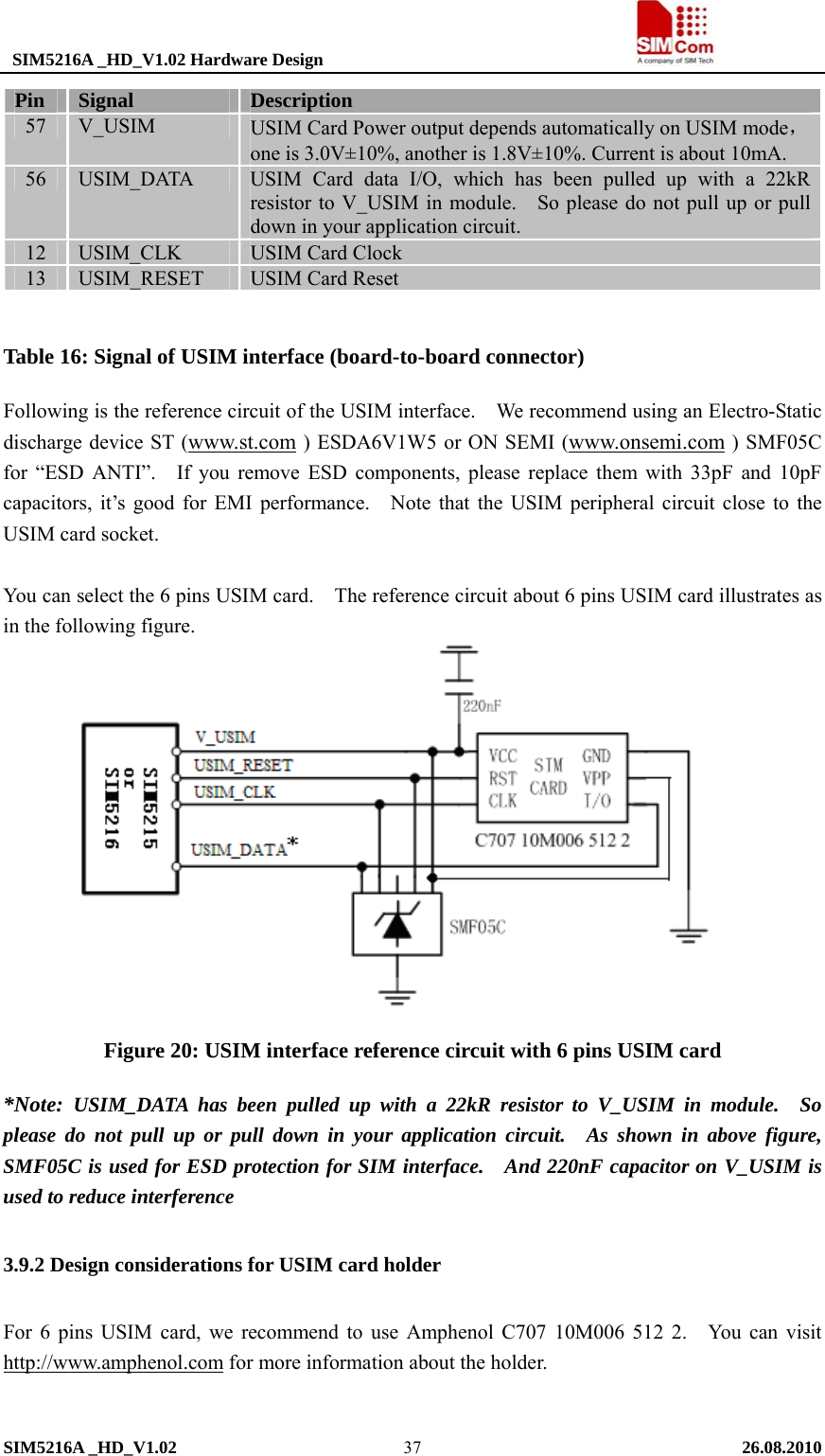
![SIM5216A _HD_V1.02 Hardware Design SIM5216A _HD_V1.02 26.08.2010 363.8.5.4 Adjust the sound level by AT+CVLVL There are two adjustable amplifiers on audio signal output path: <rxVol>, <rxGain>. Four AT commands are provided for tune them.. <rxVol>: AT+CLVL, AT+CVLVL,AT+CRXVOL <rxGain>: AT+CRXGAIN AT+CRXVOL is used for fine tuning for <rxVol>. AT+CLVL and AT+CVLVL are used for coarse tuning for <rxVol>. AT+CVLVL changes the sound level values of the command CLVL. Now we provide 5 levels for each audio channel. The level 0 is muted and it can not be changed by CVLVL. Levels 1 to 4 are supported to change the value of sound level. CVLVL command could let you change these four levels. The bigger the number presents the louder the voice. And the range of each level is -5000 to 5000. NOTE: This command influences digital volume of output signal after speech decoder. Please check the reference document [1] for detailed information of each AT command. 3.9 USIM card interface 3.9.1 USIM card application You can use AT Command to get information in USIM card. For more information, please refer to document [1]. The universal subscriber identification module (USIM) is a smart card for UMTS/GSM cellular applications. The USIM provides the required subscription information to allow the mobile equipment to attach to a GSM or UMTS network. The USIM also provides the subscriber's verification procedures as well as authentication methods for network authentication during the attach procedures. The USIM card can be inserted into any UMTS/GSM USIM equipped handset, allowing the user to receive or make calls, and receive other subscribed services from any USIM equipped handset, thus enabling more handset independence for the user. Both 1.8V and 3.0V SIM Cards are supported. The SIM interface is powered from an internal regulator in the module having nominal voltage 2.8V. All pins reset as outputs driving low. Logic levels are as described in the table below. Table 15: USIM interface](https://usermanual.wiki/Simcom/1009092010008/User-Guide-1371471-Page-37.png)
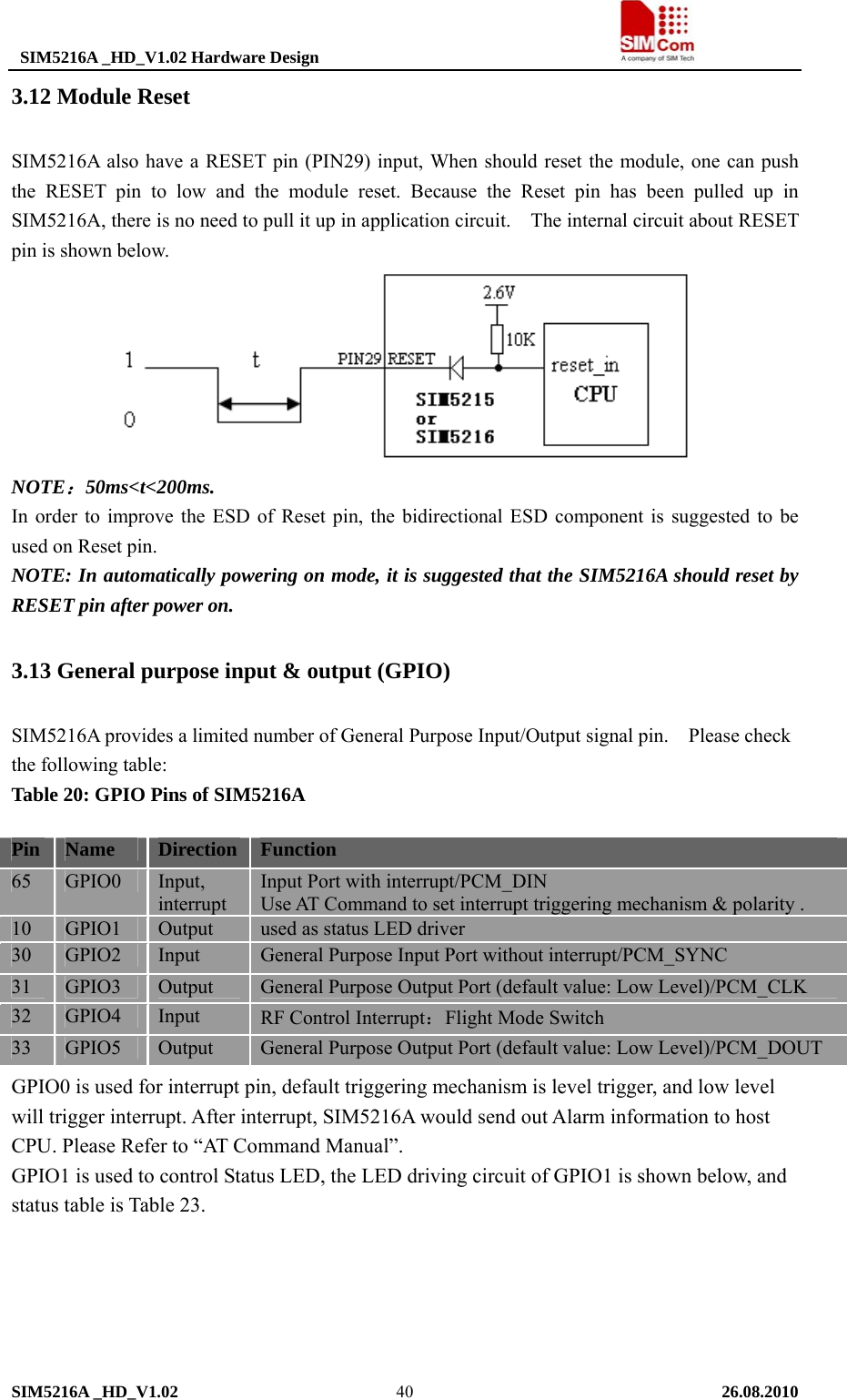
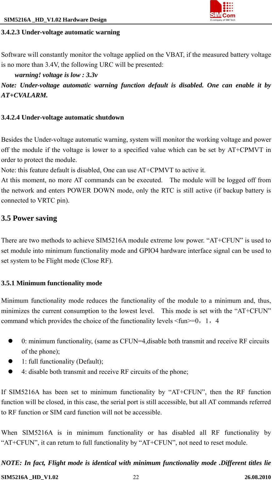
![SIM5216A _HD_V1.02 Hardware Design SIM5216A _HD_V1.02 26.08.2010 41 Figure 23: status LED circuit Notes: 300R Resistor’s value depends on LED. And status indicating table is as follow. Table 21:meanings of status LED Status Data Voice Always On Searching Network Searching Network/Call Connect 200ms ON, 200ms OFF Data Transmit 800ms ON, 800ms OFF Registered network Registered Network Off Power Off GPIO4 can be used to control RF close or on, the Flight Mode Switch logic table is shown below. You can use AT Command to read or to write GPIO2, GPIO3, GPIO5 status (High or Low level). Table 22:Logic of GPIO4 Use AT Command to read or write GPIO2, GPIO3, GPIO5 status (High or Low level). NOTE: For SIM5216A, GPIO0, GPIO2, GPIO3 and GPIO5 can be multiplex function, you can use them as PCM interface to connect extend codec. Please refer section 3.18 and document [1] for detail information. GPIO4 Status Module Action L Flight Mode: RF is closed. H Normal Mode: RF is working.](https://usermanual.wiki/Simcom/1009092010008/User-Guide-1371471-Page-42.png)
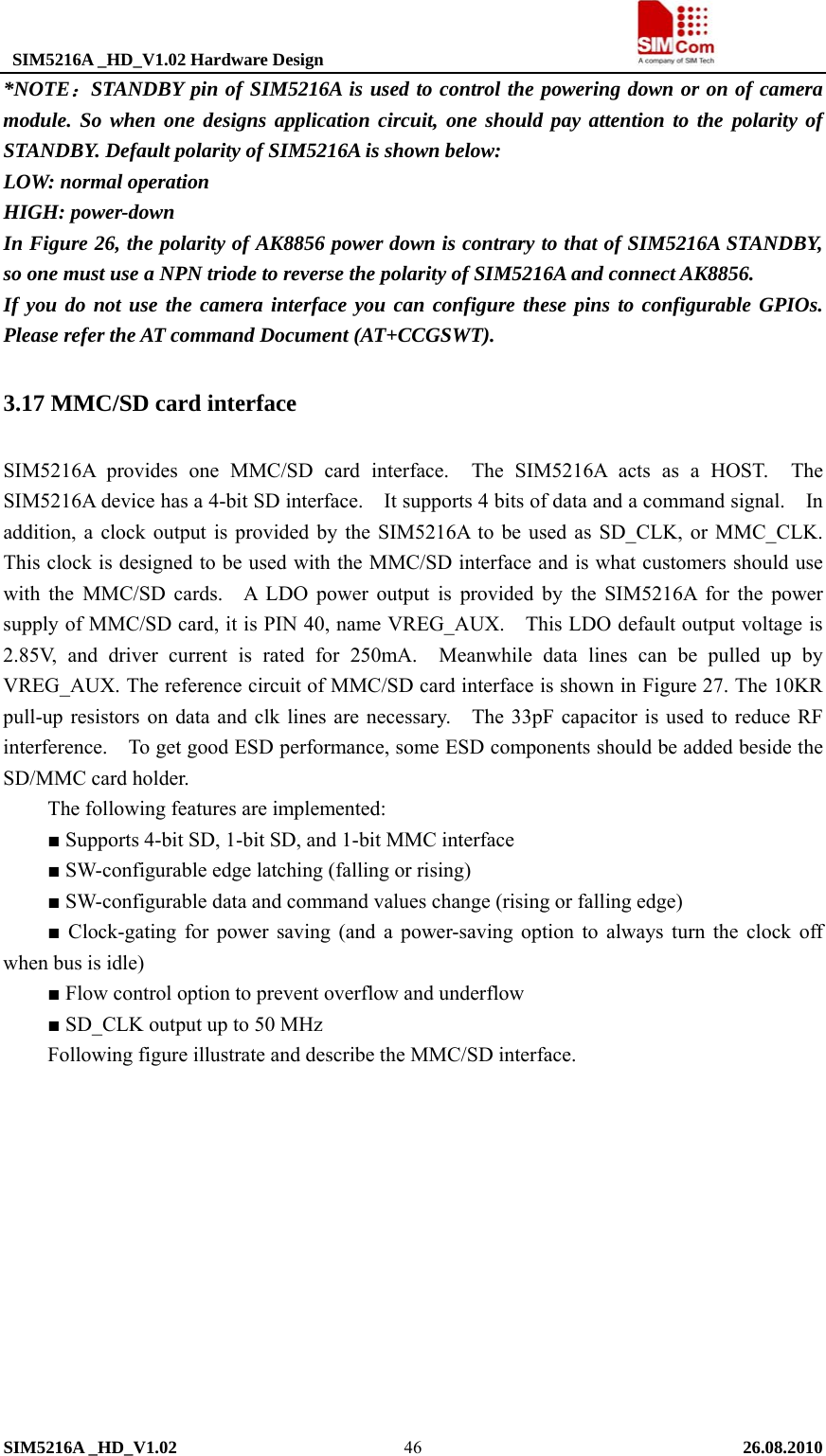
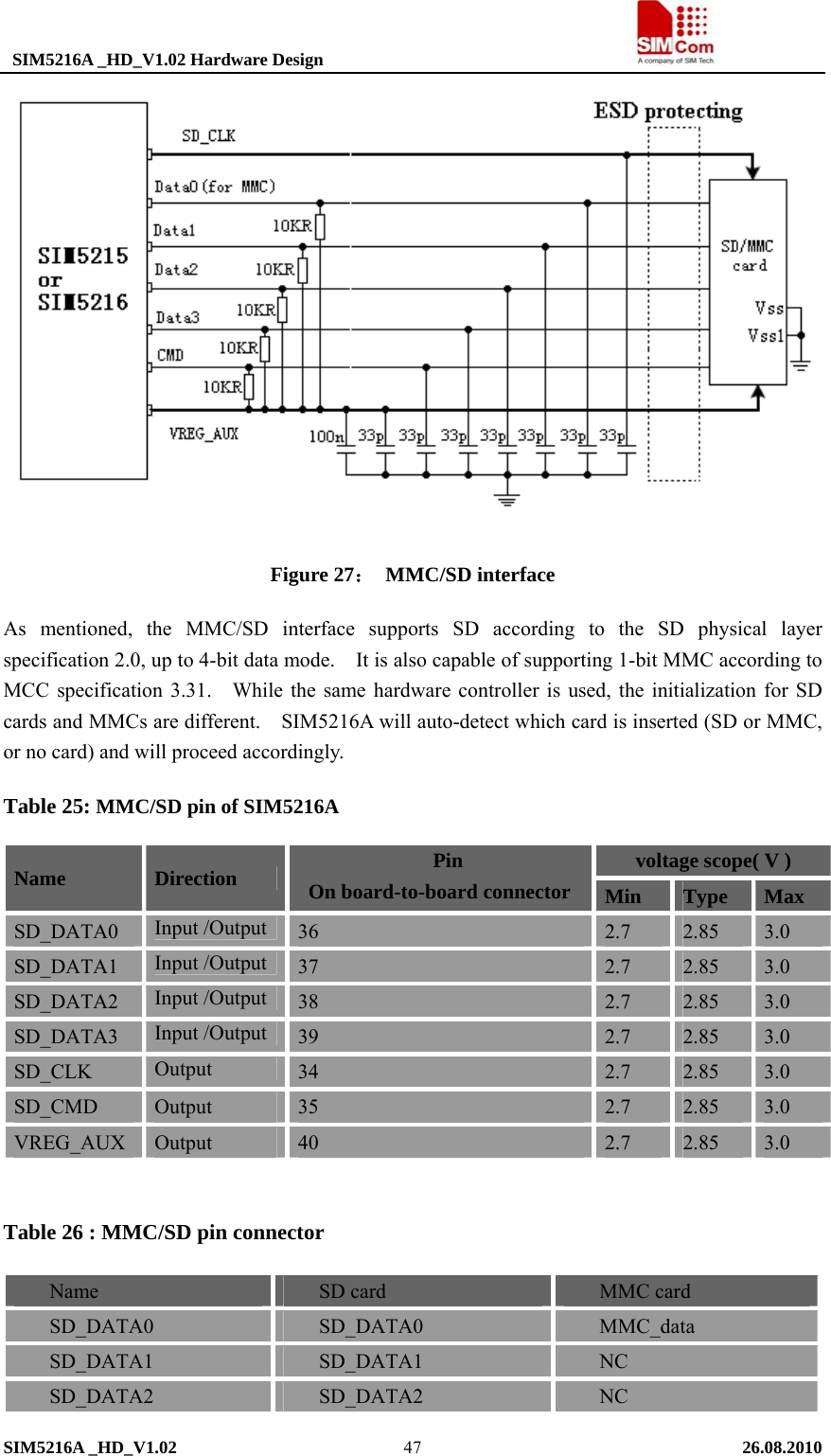
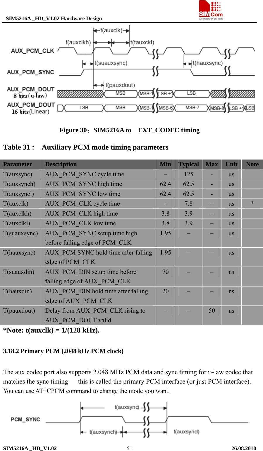
![SIM5216A _HD_V1.02 Hardware Design SIM5216A _HD_V1.02 26.08.2010 48SD_DATA3 SD_DATA3 NC SD_CLK SD_CLK MMC_CLK SD_CMD SD_CMD MMC_CMD VREG_AUX SD_VDD MMC_VDD Note: SD card interface function is supported by SIM5216A software. You can use VREG_AUX for power supply of SD card and as the pull up power for data lines. 3.18 PCM Interface SIM5216A provides hardware PCM interface for external codec. PCM interface pins are multiplex on GPIOs(default setting). Use AT+CPCM command to change pins function between PCM function and GPIOs.If enbale PCM function ,AT+CPCM command can be used to configure the PCM mode user want. Also the slot of PCM can be configured by AT+CPCMSLOT. SIM5216A PCM interface can be used in two modes: 1) the default mode is its auxiliary PCM (8 kHz long sync mode at 128kHz clk); 2) the other mode is its primary PCM (8 kHz short sync mode at 2048 kHz clk). In short-sync (primary PCM) mode, the SIM5216A can be a master or a slave. In long-sync (auxiliary PCM) mode, the SIM5216A is always a master; there is no slave support. SIM5216A support 3 PCM formats: 8 bits (υ-law or A-law) and 16 bits (linear). The PCM interface is a 4 pin, digital interface that enables PCM communication between the Module and an external codec or DSP. Both the PCM interface modes, auxiliary and primary, use the same SIM5216A pins. The PCM pin assignment is shown in the table below. Note: Please reference document [22] for detailed information of PCM Application Note. Table 27 : PCM pin assignment Pins Pin No. AUX_PCM functionality Primary_PCM functionality Description PCM_CLK/GPIO3 31 AUX_PCM_CLK PCM_CLK PCM clock for PCM communication to external codec PCM_SYNC/GPIO2 30 AUX_PCM_SYNC PCM_SYNC PCM data strobe for PCM communication to PCM mode SYNC CLK MODE Format Slot Auxiliary 8KHz 128KHz Master Only slot 0 Primary 8KHz 2.048MHz Slave/MasterA-law(8 bits)υ-law(8bits) linear(16 bits) 0~15(Changed by AT command:at+cpcmslot) Default:slot 0](https://usermanual.wiki/Simcom/1009092010008/User-Guide-1371471-Page-49.png)
![SIM5216A _HD_V1.02 Hardware Design SIM5216A _HD_V1.02 26.08.2010 49external codec PCM_DIN/GPIO0 65 AUX_PCM_DIN PCM_DIN PCM data input to the Module (Rx) PCM_DOUT/GPIO5 33 AUX_PCM_DOUT PCM_DOUT PCM data output from the Module (Tx) The default PCM interface on power up is the auxiliary PCM interface. Under PCM, the data is output on the rising edge of PCM_CLK and sampled at the falling edge of PCM_CLK. Primary PCM is disabled at power up or when RESET is asserted, but you can use AT command to enable the primary PCM mode. PCM Interface can be operated in Master and Slave mode. When the PCM interface is configured, PCM Tx data will be routed from the external codec Mic through the DSP encode path in the Module. PCM Rx data will be routed through the DSP decode path to the external codec speaker. When using the PCM Interface, the Module can be set either into Master Mode or Slave Mode. In Master Mode, the Module drives the clock and sync signals that are sent out to the external codec via the PCM Interface. When in Slave Mode, the external codec drives the clock and sync signals that are sent to the Module. Configuration Mode can be selected either primary or auxiliary. Primary configuration mode uses 2.048MHz clock and 8 kHz short sync clock, and auxiliary configuration mode uses 128KHz clock and 8 kHz long sync clock. One important consideration is that Slave mode is only available for use with Primary configuration Mode. PCM formats can also be chosen by AT command. In the default configuration, Module is the Auxiliary Master. Many parameters of external codec audio channel are not available. Only RxVolume, FIR, are still available after enabling PCM. Table 30: PCM external codec Characteristics Audio Device no. AT+CSDVC= 4 Name External Codec micAmp No available txGain No available txVol No available Default MIC path Parameters txFilter [tap0~6]0xff33, 0x05d8,0xf488, 0x0af3, 0x24bb, 0xca42,0x7c95 rxGain No available rxVol -100 stGain No available Default Output path Parameters rxFilter [tap0~6]0xff00, 0xfac9,0x0571, 0xf365, 0x0bc2, 0xf2bb,0x533a](https://usermanual.wiki/Simcom/1009092010008/User-Guide-1371471-Page-50.png)
![SIM5216A _HD_V1.02 Hardware Design SIM5216A _HD_V1.02 26.08.2010 50Default values of sound level (level 1 to 4) 0 0 0 0 NOTE: Please check the reference document [1] for detailed information of each AT command. Both PCM modes are discussed in this section, followed by additional PCM topics. 3.18.1 Auxiliary PCM (128 kHz PCM clock) The auxiliary PCM interface enables communication with an external codec to support hands-free applications. υ-law codec are supported by the auxiliary PCM interface. The auxiliary codec port operates with standard long-sync timing and a 128 kHz clock. The AUX_PCM_SYNC runs at 8 kHz with 50% duty cycle. Most υ-law codec support the 128 kHz clock. Figure 28:AUX_PCM_SYNC timing Figure 29:EXT_CODEC to SIM5216A timing](https://usermanual.wiki/Simcom/1009092010008/User-Guide-1371471-Page-51.png)
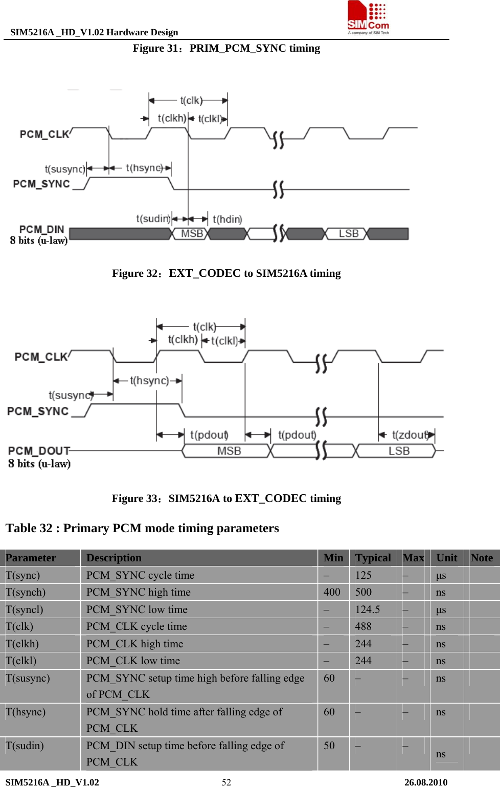
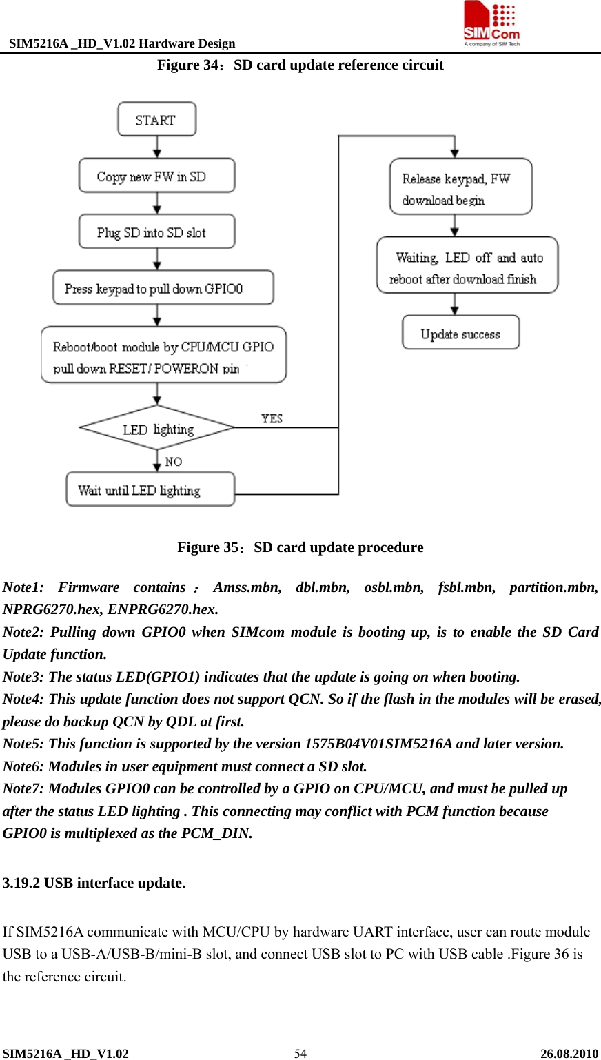
![SIM5216A _HD_V1.02 Hardware Design SIM5216A _HD_V1.02 26.08.2010 53T(hdin) PCM_DIN hold time after falling edge of PCM_CLK 10 – – ns T(pdout) Delay from PCM_CLK rising to PCM_DOUT valid – – 350 ns T(zdout) Delay from PCM_CLK falling to PCM_DOUT HIGH-Z – 160 – ns 3.18.3 Transmitting PCM data by USB Not only by hardware PCM interface, but also SIM5216A can transmit PCM data by USB. To transmit PCM data by USB, one should make sure that driver of SIM5216A has be loaded on host part. Then the NEMA port of SIM5216A can be recognized by host. One can switch it from NEMA port mode to data mode or from data mode to NEMA port mode by AT+DSWITCH. In data mode, one can control sending and receiving PCM data by AT+CPCMREG. Note: For 5213/5214/5215/5216, NEMA port is used to transmit PCM data.Please reference document [22] for detailed information of PCM Application Note. 3.19 Firmware update If SIM5216A modules are embed into user’s equipment and can’t be taken out easily, modules provide two firmware update methods that called SD card update and USB interface update. 3.19.1 SD Card update SD card update means that user can use SD card which the new firmware has been put in the SIM5216A modules to update the old Firmware .](https://usermanual.wiki/Simcom/1009092010008/User-Guide-1371471-Page-54.png)