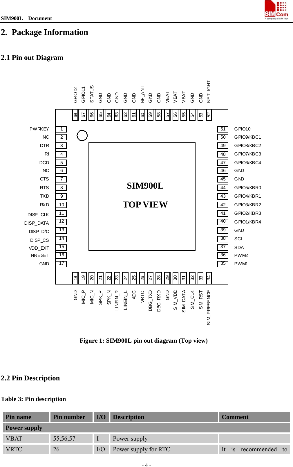
Simcom 2011091410099 GSM/GPRS Module User Manual SIM900L Rev 3

Shanghai Simcom Ltd. GSM/GPRS Module SIM900L Rev 3

Users Manual

SIM900L Document                                                                                   - 1 - SIM900L User Manual Note: This device complies with part 15 Rules. Operation is subject to the following two conditions: (1) This device may not cause harmful interference, and (2) this device must accept any interference received, including interference that may cause undesired operation. If this equipment is installed in a host, We can find the ID label when opening the host. For label requirement when transmitter module is installed in a host, the host shall have an additional permanent label referring to the enclosed module:“Contains Transmitter Module FCC ID: UDV-2011091410099” or “Contains FCC ID: UDV-2011091410099”. This equipment has a GSM antenna, and the GSM antenna peak gain is 3 dBi and modulation type is GMSK. WARNING: Changes or modifications to this unit not expressly approved by the party responsible for compliance could void the user's authority to operate the equipment. The antenna of the product, under normal use condition is at least 23.21 cm away from the body of the user,the user must keeping at least 23.21cm distance to the antenna. The device has been evaluated to meet general RF exposure requirement. The device can be used in portable exposure condition without restriction.       1. SIM900L Description 1.1 Summarize Designed for global market, SIM900L is a quad-band GSM/GPRS module that works on frequencies GSM 850MHz, EGSM 900MHz, DCS 1800MHz and PCS 1900MHz. SIM900L features GPRS multi-slot class 10/ class 8 (optional) and supports the GPRS coding schemes CS-1, CS-2, CS-3 and CS-4.  With a tiny configuration of 24*24*3mm, SIM900L can meet almost all the space requirements in user applications, such as M2M, smart phone, PDA and other mobile devices.  SIM900L has 68 SMT pads, and provides all hardware interfaces between the module and customers’ boards.  z Serial port and debug port can help user easily develop user’s applications.  z Audio channel which includes a microphone input and a receiver output.   z Programmable general purpose input and output. z The keypad and SPI display interfaces will give users the flexibility to develop customized applications.  SIM900L is designed with power saving technique so that the current consumption is as low as 1.0mA in sleep mode.   SIM900L integrates TCP/IP protocol and extended TCP/IP AT commands which are very useful for data transfer applications.
SIM900L  Document                                                                                - 2 - 1.2 SIM900L Key Features Table 1: SIM900L key features Feature  Implementation Power supply  3.4V ~ 4.5V Power saving  Typical power consumption in sleep mode is 1.0mA ( BS-PA-MFRMS=9 ) Frequency bands z SIM900L Quad-band: GSM 850, EGSM 900, DCS 1800, PCS 1900. SIM900L can search the 4 frequency bands automatically. The frequency bands also can be set by AT command “AT+CBAND”. For details, please refer to document [1]. z Compliant to GSM Phase 2/2+ Transmitting power   z Class 4 (2W) at GSM 850 and EGSM 900 z Class 1 (1W) at DCS 1800 and PCS 1900 GPRS connectivity z GPRS multi-slot class 10(default) z GPRS multi-slot class 8 (option) Temperature range   z Normal operation: -20°C ~ +60°C z Restricted operation: -40°C ~ -20°C and +60 °C ~ +85°C* z Storage temperature -45°C ~ +90°C Data GPRS z GPRS data downlink transfer: max. 85.6 kbps   z GPRS data uplink transfer: max. 42.8 kbps   z Coding scheme: CS-1, CS-2, CS-3 and CS-4 z Integrate the TCP/IP protocol. z Support Packet Broadcast Control Channel (PBCCH) CSD  z Support CSD transmission USSD  z Unstructured Supplementary Services Data (USSD) support SMS z MT, MO, CB, Text and PDU mode z SMS storage: SIM card FAX  Group 3 Class 1 SIM interface  Support SIM card: 1.8V, 3V External antenna  Antenna pad Audio features Speech codec modes: z Half Rate (ETS 06.20) z Full Rate (ETS 06.10) z Enhanced Full Rate (ETS 06.50 / 06.60 / 06.80) z Adaptive multi rate (AMR) z Echo Cancellation z Noise Suppression Serial port and   debug port Serial port: z Full modem interface with status and control lines, unbalanced, asynchronous. z 1200bps to 115200bps.
SIM900L  Document                                                                                - 3 - z Can be used for AT commands or data stream.   z Support RTS/CTS hardware handshake and software ON/OFF flow control. z Multiplex ability according to GSM 07.10 Multiplexer Protocol. z Autobauding supports baud rate from 1200 bps to 57600bps. Debug port: z Null modem interface GPS/DBG_TXD and GPS/DBG_RXD. z Can be used for debugging and upgrading firmware. Phonebook management  Support phonebook types: SM, FD, LD, RC, ON, MC. SIM application toolkit  GSM 11.14 Release 99 Real time clock  Support RTC Physical characteristics  Size: 24*24*3mm Weight: 3.4g Firmware upgrade  Firmware upgradeable by debug port. *SIM900L does work at this temperature, but some radio frequency characteristics may deviate from the GSM specification. Table 2: Coding schemes and maximum net data rates over air interface Coding scheme 1 timeslot  2 timeslot 4 timeslot CS-1  9.05kbps  18.1kbps  36.2kbps CS-2  13.4kbps  26.8kbps  53.6kbps CS-3  15.6kbps  31.2kbps  62.4kbps CS-4  21.4kbps  42.8kbps  85.6kbps
SIM900L  Document                                                                                - 4 - 2. Package Information 2.1 Pin out Diagram  GPIO12GPIO11STATUSGNDGNDGNDGNDGNDRF _A NTGNDGNDVBATVBATVBATGNDGNDNETLIGHTPWRKEY GPIO10NC GPIO9/KBC1DTR GPIO8/KBC2RI GPIO7/KBC3DCD GPIO6/KBC4NC GNDCTS GNDRTS GPIO5/KBR0TXD GPIO4/KBR1RX D GPIO3/KBR2GPIO2/KBR3GPIO1/KBR4GNDSCLSDANRESET PWM2GND PWM1GNDMIC_PMIC_NSPK_PSPK_NLINEIN_RLINEIN_LADCVRTCDBG_TXDDBG_RXDGNDSIM_VDDSIM_DATASIM_CLKSIM_RSTSIM_PRESENCEVDD_EXTDISP_CLKDISP_DATADISP_D/CDISP_CS68676665585764636261521515655545360592503494485476467459438SIM900TOP VIEW4411 4110 4212 4013 3914 3815 3716 3617 351819202122232425262728293430313233 Figure 1: SIM900L pin out diagram (Top view)  2.2 Pin Description Table 3: Pin description Pin name  Pin number  I/O  Description  Comment Power supply VBAT  55,56,57  I  Power supply   VRTC  26  I/O  Power supply for RTC  It is recommended to SIM900L TOP VIEW
SIM900L  Document                                                                                - 5 - connect with a battery or a capacitor (e.g. 4.7uF). VDD_EXT  15  O  2.8V output power supply  If it is unused, keep open.GND 17,18,29,39, 45,46,53,54, 58,59,61,62, 63,64,65  Ground   Power on/down PWRKEY  1  I PWRKEY should be pulled low at least 1 second and then released to power on/down the module.   Pulled up internally. Audio interfaces MIC_P  19 MIC_N  20 I  Differential audio input SPK_P  21 SPK_N  22 O  Differential audio output LINEIN_R  23 LINEIN_L  24 I  Line-in input If these pins are unused, keep open. Status STATUS  66  O  Power on status NETLIGHT  52  O  Network status If these pins are unused, keep open. LCD interface DISP _CLK  11  O  DISP_DATA  12  I/O  DISP _D/C  13  O DISP _CS    14  O Display interface  If these pins are unused, keep open. I2C interface SDA  37  O   I2C serial bus data SCL  38  I/O  I2C serial bus clock   If these pins are unused, keep open. Keypad interface / GPIOs GPIO5/KBR0 44  GPIO5/keypad row 0 GPIO4/KBR1  43  GPIO4/keypad row 1 GPIO3/KBR2  42  GPIO3/keypad row 2 GPIO2/KBR3  41  GPIO2/keypad row 3 GPIO1/KBR4  40  GPIO1/keypad row 4 GPIO9/KBC1 50  GPIO9/keypad column 1 GPIO8/KBC2  49  GPIO8/keypad column 2 GPIO7/KBC3  48  GPIO7/keypad column 3 GPIO6/KBC4  47  GPIO6/keypad column 4 GPIO10  51 I/O GPIO10 If these pins are unused, keep open.
SIM900L  Document                                                                                - 6 - GPIO11  67  GPIO11 GPIO12  68  GPIO12 Serial port RXD  10  I  Receive data This pin should be pulled up to VDD_EXT externally.   TXD  9  O  Transmit data RTS  8  I  Request to send CTS  7  O  Clear to send DCD  5  O  Data carrier detect   RI   4  O  Ring indicator   DTR  3  I  Data terminal ready If these pins are unused, keep open. Debug interface DBG_TXD  27  O DBG_RXD  28  I For debugging and upgrading firmware If these pins are unused, keep open. SIM interface SIM_VDD  30  O  Voltage supply for SIM card. Support 1.8V or 3V SIM card SIM_DATA  31  I/O  SIM data input/output SIM_CLK  32  O  SIM clock SIM_RST  33  O  SIM reset All signals of SIM interface should be protected against ESD with a TVS diode array. SIM_PRESENCE  34  I  SIM card detection  If it is unused, keep open.ADC ADC  25  I  Input voltage range: 0V ~ 2.8V  If it is unused, keep open.External reset NRESET  16  I  Reset input(Active low)  Recommend connecting a 100nF capacitor. Pulse width modulation( PWM ) PWM1  35  O  PWM PWM2  36  O  PWM  If these pins are unused, keep open. RF interface RF_ANT  60  I/O  Radio antenna connection  Impendence must be controlled to 50Ω. Not connect NC  2,6  -   These pins should be kept open.
SIM900L  Document                                                                                - 7 - .3 Package Dimensions TOP VIEW BOTTOM VIEW Figure 2: Dimensions of SIM900L(Unit: mm)   Figure 3: Recommended PCB footprint outline(Unit: mm)
SIM900L  Document                                                                                - 8 - 2.4 Pictures  Figure 4: the top view of SIM900L
SIM900L  Document                                                                                - 9 - 3. Detail Block Diagram  Figure 5: Block diagram of SIM900L   4. Electrical and Reliability Characteristics 4.1 Absolute Maximum Ratings The absolute maximum ratings stated in following table are stress ratings under non-operating conditions. Stresses beyond any of these limits will cause permanent damage to SIM900L.  Table 4: Absolute maximum ratings Symbol  Parameter  Min  Typ  Max  Unit VBAT  Power supply voltage  -  -  5.5  V VI* Input voltage  -0.3  -  3.1  V II* Input current  -  -  10  mA IO* Output current  -  -  10  mA *These parameters are for digital interface pins, such as keypad, GPIO, I2C, UART, LCD, PWMs and DEBUG. 26M 32K FLASHApplication Interface (68PIN,SMT TYPE) A[0:21]D[0:16]UART DBGVBACKUPGPIOSPIAUDIOVEXTKEYPADPWRKEYPAM(PA+SW ITCH)     RF7161              PNX4851 Intergrading DBB,ABB and TransceiverSAW Filter Antenna PAD
SIM900L  Document                                                                                - 10 - 4.2 Recommended Operating Conditions Table 5: Recommended operating conditions Symbol  Parameter  Min  Typ  Max  Unit VBAT  Power supply voltage  3.2  4.0  4.8  V TOPER Operating temperature  -40  +25  +85  ℃ TSTG Storage temperature  -45   +90  ℃ 4.3 Digital Interface Characteristics Table 6: Digital interface characteristics Symbol  Parameter  Min  Typ  Max  Unit IIH High-level input current  -10  -  10  uA IIL Low-level input current  -10  -  10  uA VIH High-level input voltage  2.4  -  -  V VIL Low-level input voltage  -  -  0.4  V VOH High-level output voltage  2.7  -  -  V VOL Low-level output voltage  -  -  0.1  V * These parameters are for digital interface pins, such as keypad, GPIO, I2C, UART, LCD, PWMs and DEBUG. 4.4 SIM Card Interface Characteristics Table 7: SIM card interface characteristics Symbol  Parameter  Min  Typ  Max  Unit IIH High-level input current  -10  -  10  uA IIL Low-level input current  -10  -  10  uA 1.4  -  -  V VIH High-level input voltage 2.4  -  -  V -  -  0.4  V VIL Low-level input voltage   2.4  V 1.7  -  -  V VOH High-level output voltage 2.7  -  -  V -  -  0.1  V VOL Low-level output voltage -  -  0.1  V 4.5 VDD_EXT Characteristics
SIM900L  Document                                                                                - 11 - Table 8: VDD_EXT characteristics Symbol  Parameter  Min  Typ  Max  Unit VO Output voltage  2.70  2.80  2.95  V IO Output current  -  -  10  mA 4.6 SIM_VDD Characteristics Table 9: SIM_VDD characteristics Symbol  Parameter  Min  Typ  Max  Unit 2.75  2.9  3.00 VO Output voltage 1.65  1.80  1.95 V IO Output current  -  -  10  mA 4.7 VRTC Characteristics Table 10: VRTC characteristics Symbol  Parameter  Min  Typ  Max  Unit VRTC-IN VRTC input voltage  2.00  3.00  3.15  V IRTC-IN VRTC input current  -  2  -  uA VRTC-OUT VRTC output voltage  -  3.00  -  V IRTC-OUT VRTC output current  -  10  -  uA  4.8 Current Consumption (VBAT = 3.8V, GPS engine is powered down) Table 11: GSM current consumption Symbol  Parameter  Conditions  Value  Unit IVRTC VRTC current  VBAT disconnects. Backup battery is 3 V  2  uA Power down mode  30  uA BS-PA-MFRMS=9  1.0 BS-PA-MFRMS=5  1.2 Sleep mode BS-PA-MFRMS=2  1.5 mA GSM 850 EGSM 900 DCS 1800 Idle mode PCS 1900 22  mA IVBAT VBAT current Voice call  GSM 850  PCL=5  250  mA
SIM900L  Document                                                                                - 12 - PCL=12  110 EGSM 900 PCL=19  76 PCL=0  168 PCL=7  89 DCS 1800 PCS 1900 PCL=15  76 PCL=5  240 PCL=12  110 GSM 850 EGSM 900 PCL=19  83 mA PCL=0  170 PCL=7  95 Data mode GPRS(1Rx,1Tx) DCS 1800 PCS 1900 PCL=15  80 mA PCL=5  270 PCL=12  150 GSM 850 EGSM 900 PCL=19  120 mA PCL=0  205 PCL=7  130 Data mode GPRS(4Rx,1Tx) DCS 1800 PCS 1900 PCL=15  115 mA PCL=5  440 PCL=12  185 GSM 850 EGSM 900 PCL=19  130 mA PCL=0  300 PCL=7  155 Data mode GPRS(3Rx,2Tx) DCS 1800 PCS 1900 PCL=15  122 mA IVBAT-peak Peak current    During Tx burst  2  A  4.9 Electro-Static Discharge SIM900L is an ESD sensitive component, so more attention should be paid to the procedure of handling and packaging. The ESD test results are shown in the following table. Table 12: The ESD characteristics (Temperature: 25 , Humidity: 45 %)℃ Pin  Contact discharge  Air discharge VBAT  ±5KV  ±10KV GND  ±4KV  ±10KV RXD, TXD  ±3KV  ±6KV Antenna port  ±5KV  ±10KV SPKP/ SPKN MICP/ MICN  ±2KV  ±8KV PWRKEY  ±1KV  ±8KV
SIM900L  Document                                                                                - 13 - 4.10 Radio Characteristics 4.10.1 Module RF Output Power The following table shows the module conducted output power, it is followed by the 3GPP TS 05.05 technical specification requirement. Table 13: SIM900L GSM 900 and GSM 850 conducted RF output power GSM 900 and EGSM 850 Tolerance (dB) for conditions PCL  Nominal output power (dBm)  Normal  Extreme 0-2  39  ±2  ±2.5 3  37  ±3  ±4 4  35  ±3  ±4 5  33  ±3  ±4 6  31  ±3  ±4 7  29  ±3  ±4 8  27  ±3  ±4 9  25  ±3  ±4 10  23  ±3  ±4 11  21  ±3  ±4 12  19  ±3  ±4 13  17  ±3  ±4 14  15  ±3  ±4 15  13  ±3  ±4 16  11  ±5  ±6 17  9  ±5  ±6 18  7  ±5  ±6 19-31  5  ±5  ±6 Table 14: SIM900L DCS 1800 and PCS 1900 conducted RF output power DCS 1800 and PCS 1900 Tolerance (dB) for conditions PCL  Nominal output power (dBm)  Normal  Extreme 29  36  ±2  ±2.5 30  34  ±3  ±4 31  32  ±3  ±4 0  30  ±3  ±4 1  28  ±3  ±4
SIM900L  Document                                                                                - 14 - 2  26  ±3  ±4 3  24  ±3  ±4 4  22  ±3  ±4 5  20  ±3  ±4 6  18  ±3  ±4 7  16  ±3  ±4 8  14  ±3  ±4 9  12  ±4  ±5 10  10  ±4  ±5 11  8  ±4  ±5 12  6  ±4  ±5 13  4  ±4  ±5 14  2  ±5  ±6 15-28  0  ±5  ±6  For the module’s output power, the following is should be noted:   At GSM900 and GSM850 band, the module is a class 4 device, so the module’s output power should not exceed 33dBm, and at the maximum power level, the output power tolerance should not exceed +/-2dB under normal condition and +/-2.5dB under extreme condition.  At DCS1800 and PCS1900 band, the module is a class 1 device, so the module’s output power should not exceed 30dBm, and at the maximum power level, the output power tolerance should not exceed +/-2dB under normal condition and +/-2.5dB under extreme condition. 4.10.2 Module RF Receive Sensitivity The following table shows the module’s conducted receive sensitivity, it is tested under static condition. Table 15: SIM900L conducted RF receive sensitivity Frequency   Receive sensitivity(Typical) Receive sensitivity(Max) GSM850  -109dBm  -107dBm EGSM900  -109dBm  -107dBm DCS1800  -109dBm  -107dBm PCS1900  -109dBm  -107dBm 4.10.3 Module Operating Frequencies The following table shows the module’s operating frequency range; it is followed by the 3GPP TS 05.05 technical specification requirement. Table 16: SIM900L operating frequencies
SIM900L  Document                                                                                - 15 - Frequency   Receive   Transmit  GSM850  869 ~ 894MHz  824 ~ 849 MHz EGSM900  925 ~ 960MHz  880 ~ 915MHz DCS1800  1805 ~ 1880MHz  1710 ~ 1785MHz PCS1900  1930 ~ 1990MHz  1850 ~ 1910MHz

Navigation menu