User Manual

SIM808 Document
- 1 -
1. SIM808 Description
1.1. Summarize
SIM808 designed by SIMCom is a quad band module which supports GSM/GPRS. The baseband circuit is
based on MTK and RF circuit is based on RFMD. It works at quad bands------GSM850, EGSM900, DCS1800,
and PCS1900. CPU clock is based on 26MHz crystal. The main IC includes MT6261D and RF7198. SIM808 is
in compliance with the essential requirements and other relevant provisions of Directive1999/5/EC .
1.2. Feature
● Quad-Band 850/900/1800/1900MHz
● GPRS multi-slot class 12
● GPRS mobile station class B
● Compliant to GSM phase 2/2+
– Class 4 (2 W @ 850/900 MHz)
– Class 1 (1 W @ 1800/1900MHz)
● 22 tracking/66 acquisition-channel GPS L1 receiver
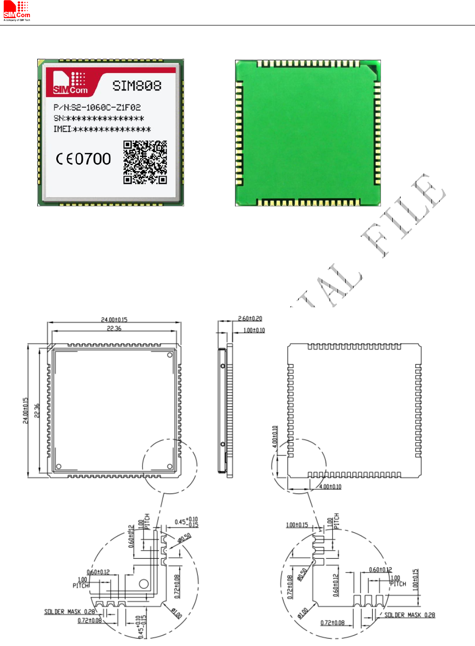
● Dimensions: 24*24*2.6 mm
● Weight: 3.3 g
● Control via AT commands (3GPP TS 27.007, 27.005 and SIMCom enhanced AT Commands)
● Supply voltage range 3.4~4.4 V
● Low power consumption
● Operation temperature:-40~85℃
● 68 SMT pads include
– Interface to external SIM 3V/1.8V
– Analog audio interface
– RTC backup
– Serial interface
– I2C interface
– USB interface
– Keypad interface
– Antenna pad
– PCM interface
– PWM
– GPIO
– ADC
– Other signal
Smart Machine Smart Decision
- 2 -
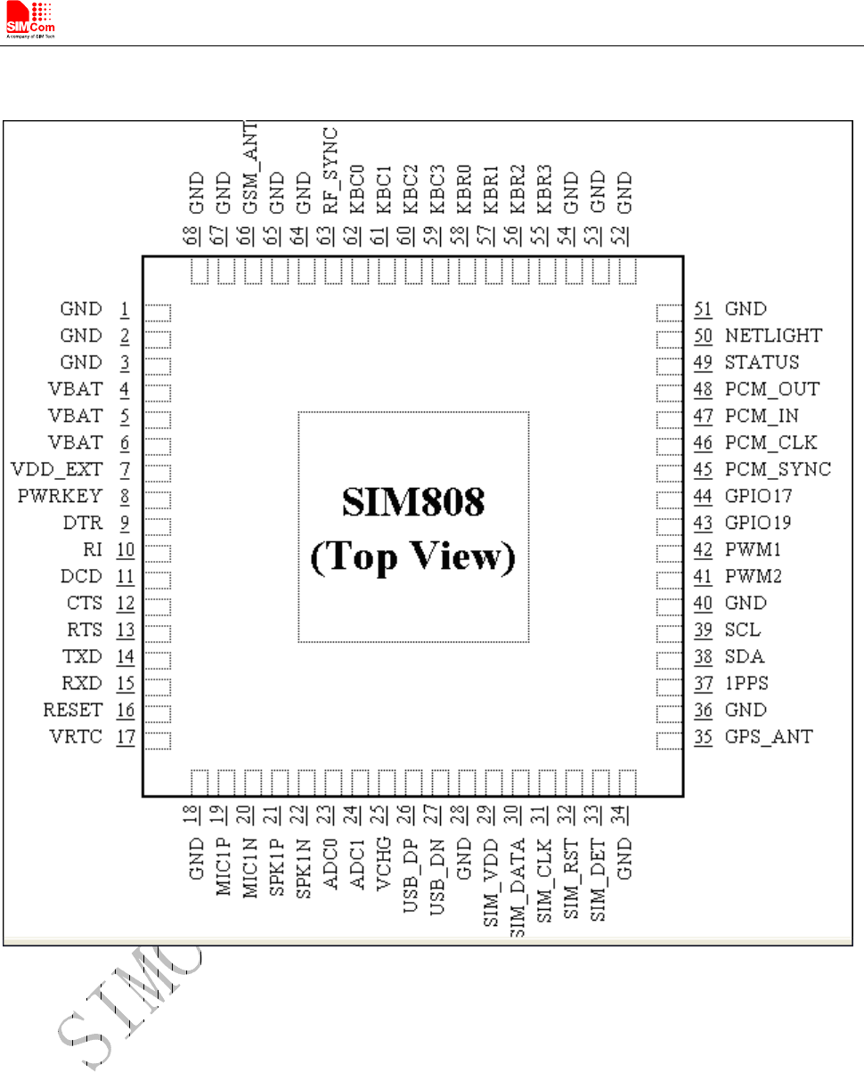
1.3. Pin
Smart Machine Smart Decision
- 3 -
1.4. Picture
Figure 1: Top and Bottom view of SIM808
1.5. Dimension
Figure 2: Dimention
Smart Machine Smart Decision
- 4 -
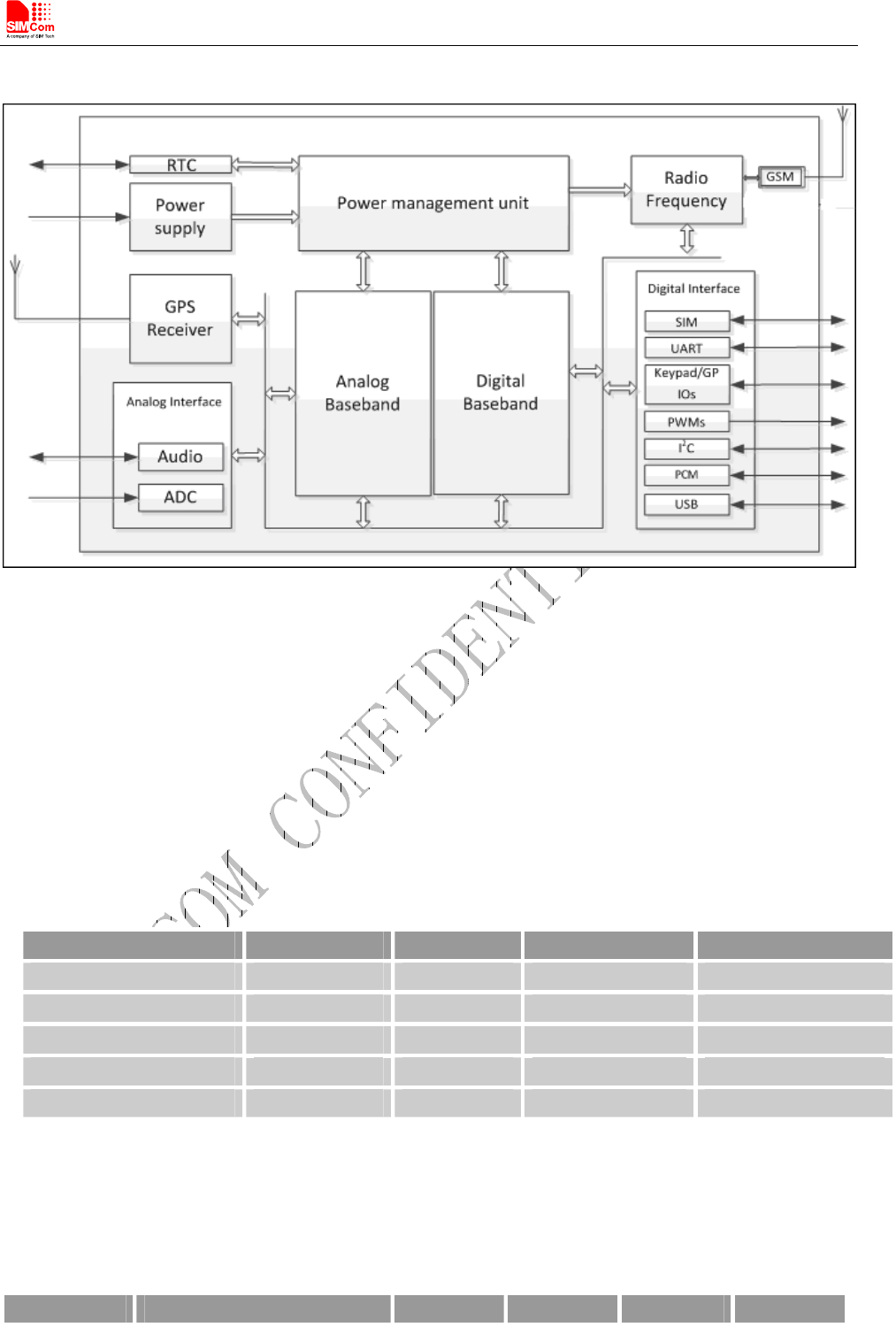
2. Detail Block Diagram
Figure 3: Block diagram of SIM808
3. Electrical and Reliability Characteristics
3.1. Absolute Maximum Ratings
The absolute maximum ratings stated in following table are stress ratings under non-operating conditions. Stresses
beyond any of these limits will cause permanent damage to SIM808.
Table 1: Absolute maximum ratings
Symbol Min Typ Max Unit
VBAT - - 4.5 V
Current 0 2.0 A
VCHG - 12 V
II
* - 4 16 mA
IO
* - 4 16 mA
*These parameters are for digital interface pins, such as keypad, GPIO, I2C, UART,PWMs and PCM.
3.2. Digital Interface Characteristics
Table 2: Digital interface characteristics
Symbol Parameter Min Typ Max Unit
Smart Machine Smart Decision
- 5 -
IIH High-level input current 2.1 - 3.1 V
IIL Low-level input current -0.3 - 0.7 V
VOH High-level input voltage 2.4 2.8 - V
VOL Low-level input voltage - - 0.4 V
* These parameters are for digital interface pins, such as keypad, GPIO, I2C, UART, PWMs and PCM.
3.3. SIM Card Interface Characteristics
Table 3: SIM card interface characteristics
Symbol Parameter Min Typ Max Unit
IIH High-level input current -1 - 1 uA
IIL Low-level input current -1 - 1 uA
1.4 - - V
VIH High-level input voltage
2.4 - - V
- - 0.27 V
VIL Low-level input voltage
0.4 V
1.62 - - V
VOH High-level output voltage
2.7 - - V
- - 0.36 V
VOL Low-level output voltage
- - 0.4 V
3.4. SIM_VDD Characteristics
Table 4: SIM_VDD characteristics
Symbol Parameter Min Typ Max Unit
3.0 V
VO Output voltage
1.8 V
IO Output current - - 10 mA
3.5. VRTC Characteristics
Table 5: VRTC characteristics
Symbol Parameter Min Typ Max Unit
VRTC-IN VRTC input voltage 1.2 2.8 3.0 V
IRTC-IN VRTC input current - 3.0 5.0- uA
VRTC-OUT VRTC output voltage - 2.8 - V
IRTC-OUT VRTC output current - 2 mA

Smart Machine Smart Decision
- 6 -
3.6. Current Consumption
Table 6: Module current consumption (VBAT = 4V, GPS engine is powered down)
Symbol
Parameter Conditions Min Typ Max Unit
Voltage 3.4 4.0 4.4 V
Voltage drop PCL=5 350 mV
VBAT
Voltage ripple PCL=5
@ f<200kHz
@ f>200kHz
50
2.0
mV
mV
Power off mode 134 150 uA
Sleep mode (AT+CFUN=1):
( BS-PA-MFRMS=9 )
( BS-PA-MFRMS=5)
( BS-PA-MFRMS=2)
1.073
1.167
1.627
mA
mA
mA
Idle mode (AT+CFUN=1):
EGSM900
16.80
mA
Voice call (PCL=5):
GSM850
EGSM900
Voice call (PCL=0):
DCS1800
PCS1900
216.6
221.7
140.3
155.0
mA
mA
mA
mA
Data mode GPRS (1Rx,4Tx):
GSM850
EGSM900
DCS1800
PCS1900
445.5
433.7
287.1
296.5
mA
mA
mA
mA
Data mode GPRS (3Rx,2Tx):
GSM850
EGSM900
DCS1800
PCS1900
332.9
333.5
222.0
229.8
mA
mA
mA
mA
IVBAT Average current
Data mode GPRS (4Rx,1Tx):
GSM850
EGSM900
DCS1800
PCS1900
222.6
224.7
158.4
165.2
mA
mA
mA
mA
IMAX Peak current During TX burst 2.0 A
Table 7: GPS current consumption
Smart Machine Smart Decision
- 7 -
Module Conditions CNo(dB/Hz) Current(mA)
Leak current when power
off Not accessible /
No Fix / 23.5
-130dBm/Tracking 38-39 21.8
-140dBm/Tracking 28-29 21.7
-150dBm/Tracking 18-19 20.6
-160dBm/Tracking 13-14 19.8
-130dBm/Cold start 41-42 24.7
-140dBm/Cold start 31-32 24.9
By
instrument
-150dBm/Cold start / 23.2
Leak current when power
off Not accessible /
No Fix / 21
Searching / 19.4
Real
networking
Fixed 35 19.7
* In above table the current consumption value is the typical one of the module tested in laboratory. In the mass
production stage, there may be differences among each individual.
3.7. Electro-Static Discharge
SIM808 is an ESD sensitive component, so more attention should be paid to the procedure of handling and
packaging. The ESD test results are shown in the following table.
Table 8: The ESD characteristics (Temperature: 25℃, Humidity: 45 %)
Pin Contact discharge Air discharge
VBAT ±5KV ±10KV
GND ±5KV ±10KV
Smart Machine Smart Decision
- 8 -
RXD, TXD ±2KV ±8KV
Antenna port ±5KV ±10KV
SPK_P/SPK_N/
MIC_P/MIC_N ±4KV ±8KV
PWRKEY ±4KV ±8KV
Note: It is suggested that customers in serials with 100ohm resistances on UART lines for ESD
consideration.
4. Radio Characteristics
4.1. Module GSM/GPRS Output Power
The following table shows the module conducted output power, it is followed by the 3GPP TS 05.05 technical
specification requirement.
Table 9: SIM808 GSM 900 and GSM 850 conducted RF output power
GSM850、EGSM900
Tolerance (dB) for conditions
PCL Nominal output power (dBm)
Normal Extreme
5 33 ±2 ±2.5
6 31 ±3 ±4
7 29 ±3 ±4
8 27 ±3 ±4
9 25 ±3 ±4
10 23 ±3 ±4
11 21 ±3 ±4
12 19 ±3 ±4
13 17 ±3 ±4
14 15 ±3 ±4
15 13 ±3 ±4
16 11 ±5 ±6
17 9 ±5 ±6
18 7 ±5 ±6
19-31 5 ±5 ±6
Table 10: SIM808 DCS 1800 and PCS 1900 conducted RF output power
DCS1800、PCS1900
PCL Nominal output power (dBm) Tolerance (dB) for conditions
Smart Machine Smart Decision
- 9 -
Normal Extreme
0 30 ±2 ±2.5
1 28 ±3 ±4
2 26 ±3 ±4
3 24 ±3 ±4
4 22 ±3 ±4
5 20 ±3 ±4
6 18 ±3 ±4
7 16 ±3 ±4
8 14 ±3 ±4
9 12 ±4 ±5
10 10 ±4 ±5
11 8 ±4 ±5
12 6 ±4 ±5
13 4 ±4 ±5
14 2 ±5 ±6
15 0 ±5 ±6
For the module’s output power, the following is should be noted:
At GSM900 and GSM850 band, the module is a class 4 device, so the module’s output power should not exceed
33dBm, and at the maximum power level, the output power tolerance should not exceed +/-2dB under normal
condition and +/-2.5dB under extreme condition.
At DCS1800 and PCS1900 band, the module is a class 1 device, so the module’s output power should not exceed
30dBm, and at the maximum power level, the output power tolerance should not exceed +/-2dB under normal
condition and +/-2.5dB under extreme condition.
The device complies with RF specifications when the device used over 20cm form your body.
4.2. Module GSM/GPRS Receive Sensitivity
The following table shows the module’s conducted receive sensitivity, it is tested under static condition.
Table 11: SIM808 conducted GSM/GPRS receive sensitivity
Frequency Receive sensitivity(Typical) Receive sensitivity(Max)
GSM850 <-108dBm <-106dBm
EGSM900 <-108dBm <-106dBm
DCS1800 <-108dBm <-106dBm
PCS1900 <-108dBm <-106dBm
Smart Machine Smart Decision
- 10 -
4.3. Module GPS Receiver Performance
The following table shows the module’s conducted TTFF(Time To First Fix) and receive sensitivity, it is tested
under static condition.
Table 12: SIM808 conducted GPS Performance
Parameter Description Performance (Type)
Autonomous acquisition(cold
start)
-148dBm
Re-acquisition -159dBm
Sensitivity
Tracking -165dBm
Hot start <1s
Warm start 28s
Time To First Fix
Clod start 30s
4.4. Module Operating Frequencies
The following table shows the module’s operating frequency range; it is followed by the 3GPP TS 05.05 technical
specification requirement.
Table 13: SIM808 operating frequencies
Frequency Receive Transmit
GSM850 869 ~ 894MHz 824 ~ 849 MHz
EGSM900 925 ~ 960MHz 880 ~ 915MHz
DCS1800 1805 ~ 1880MHz 1710 ~ 1785MHz
PCS1900 1930 ~ 1990MHz 1850 ~ 1910MHz
GPS 1575.45±2MHz N/A
5. Antenna interface
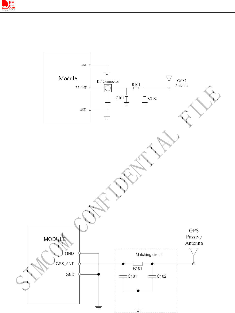
There are three antenna ports for SIM808, GSM antenna port named RF_ANT, GPS antenna port named
GPS_ANT, The RF interface of the three antenna ports has an impedance of 50Ω.The maximum gain of the
antenna gain should not exceed 3dbi considering the SAR radio.
The input impendence of the antenna should be 50Ω, and the VSWR should be less than 2.
It is recommended that the GSM antenna and the GPS antenna be placed as far as better.
The isolations of the three antenna should be bigger than 30db
5.1 GSM Antenna Interface
There is a GSM antenna pad named RF_ANT for SIM808 the connection of the antenna must be decoupled
Smart Machine Smart Decision
- 11 -
from DC voltage. This is necessary because the antenna connector is DC coupled to ground via an inductor for
ESD protection.
The external antenna must be matched properly to achieve best performance, so the matching circuit is
necessary, the connection is recommended as following:
Figure1: GSM antenna matching circuit
R101,C101,C102 are the matching circuit, the value should be defined by the antenna design. normally R101
is 0Ω, C101 和C102 are not SMD. The RF connector is used for conducted
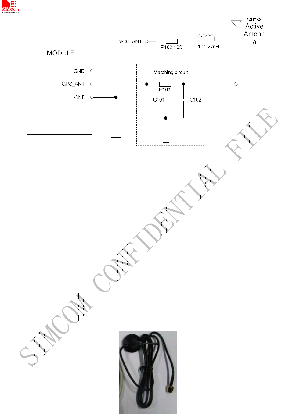
5.2 GPS antenna interface
The module provides a GPS antenna interface named GPS_ANT. There are two normal options: passive
antenna and active antenna.
The external antenna must be matched properly to achieve best performance, so the matching circuit is
necessary, the connection is recommended as following figure:
Figure 5: GPS passive antenna matching circuit
The components R101, C101 and C102 are used for antenna matching, the components’ value only can be got
after the antenna tuning. Normally R101 is 0Ω, C101 and C102 are not mounted.
Smart Machine Smart Decision
- 12 -
Figure 1: GPS active antenna matching circuit
There are some suggestions to components placing and lying for GSM and Bluetooth RF traces:
The RF connector is used for conducted test, so keep it as close as pin RF_ANT;
Antenna matching circuit should be closed to the antenna;
Keep the RF traces as 50Ω;
The RF traces should be kept far away from the high frequency signals and strong disturbing source.
5.3.1 GSM antenna
Model GSM antenna: WT-C&G-28-90
Frequency Range (MHz) 824 ~ 960 1710 ~ 1990
VSWR ≤1.5 (900MHz) ≤2 (1800MHz)
Gain (dBi): 3
Input Impedance (Ω): 50
Polarization Type: Vertical
Connector Type: SMA
Figure 7 GSM antenna
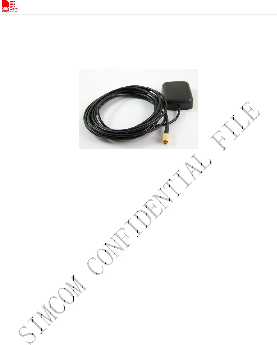
5.3.2 GPS antenna
Smart Machine Smart Decision
- 13 -
1. Frequency Range: 1575.42±3MHz
2. Impedance: 50 Ohms nominal
3. VSWR: ≦1.5
4. Gain: 3.0dBi
5. Polarization: RHCP
6. Connector Type: SMA P/S
Figure 7 GPS antenna
Federal Communication Commission Interference Statement
This device complies with Part 15 of the FCC Rules. Operation is subject to the following
two conditions: (1)This device may not cause harmful interference, and (2) this device must
accept any interference received,including interference that may cause undesired operation.
This equipment has been tested and found to comply with the limits for a Class B digital device,
pursuant toPart 15 of the FCC Rules. These limits are designed to provide reasonable protection
against harmful interference in a residential installation. This equipment generates, uses and can
radiate radio frequency energy and, if not installed and used in accordance with the instructions,
may cause harmful interference to radio communications. However, there is no guarantee that
interference will not occur in a particular installation. If this equipment does cause harmful
interference to radio or television reception, which can be determined by turning the equipment
off and on, the user is encouraged to try to correct the interference by one of the following
measures:
- Reorient or relocate the receiving antenna.
- Increase the separation between the equipment and receiver.
- Connect the equipment into an outlet on a circuit different from that
to which the receiver is connected.
- Consult the dealer or an experienced radio/TV technician for help.
FCC Caution: Any changes or modifications not expressly approved by the party responsible for
Compliancecould void the user's authority to operate this equipment.
This transmitter must not be co-located or operating in conjunction with any other antenna or
transmitter.
RF Exposure Compliance

Smart Machine Smart Decision
- 14 -
This equipment complies with FCC radiation exposure limits set forth for an uncontrolled
environment.The antenna(s) used for this transmitter must be installed to provide a separation distance of at
least20 cm from all persons and must not be co-located or operating in conjunction with any other antenna
orTransmitter.
This device is intended only for OEM integrators under the following conditions:
1) The antenna must be installed such that 20 cm is maintained between the antenna and users, and
2) The transmitter module may not be co-located with any other transmitter or antenna.
As long as 2 conditions above are met, further transmitter test will not be required. However, the OEM
integrator is stillresponsible for testing their end-product for any additional compliance requirements
required with this module installed
IMPORTANT NOTE: In the event that these conditions can not be met (for example certain laptop
configurations or co-location with another transmitter), then the FCC authorization is no longer
considered valid and the FCC ID can not be usedon the final product. In these circumstances, the OEM
integrator will be responsible for re-evaluating the end product(including the transmitter) and obtaining
a separate FCC authorization.
End Product Labeling:
This transmitter module is authorized only for use in device where the antenna may be installed such
that 20 cm may bemaintained between the antenna and users. The final end product must be labeled in a
visible area with the following: “Contains FCC ID:UDV-20160416".
Manual Information To the End User
The OEM integrator has to be aware not to provide information to the end user regarding how to install or
remove this RF module in the user’s manual of the end product which integrates this module.
The end user manual shall include all required regulatory information/warning as show in this manual.