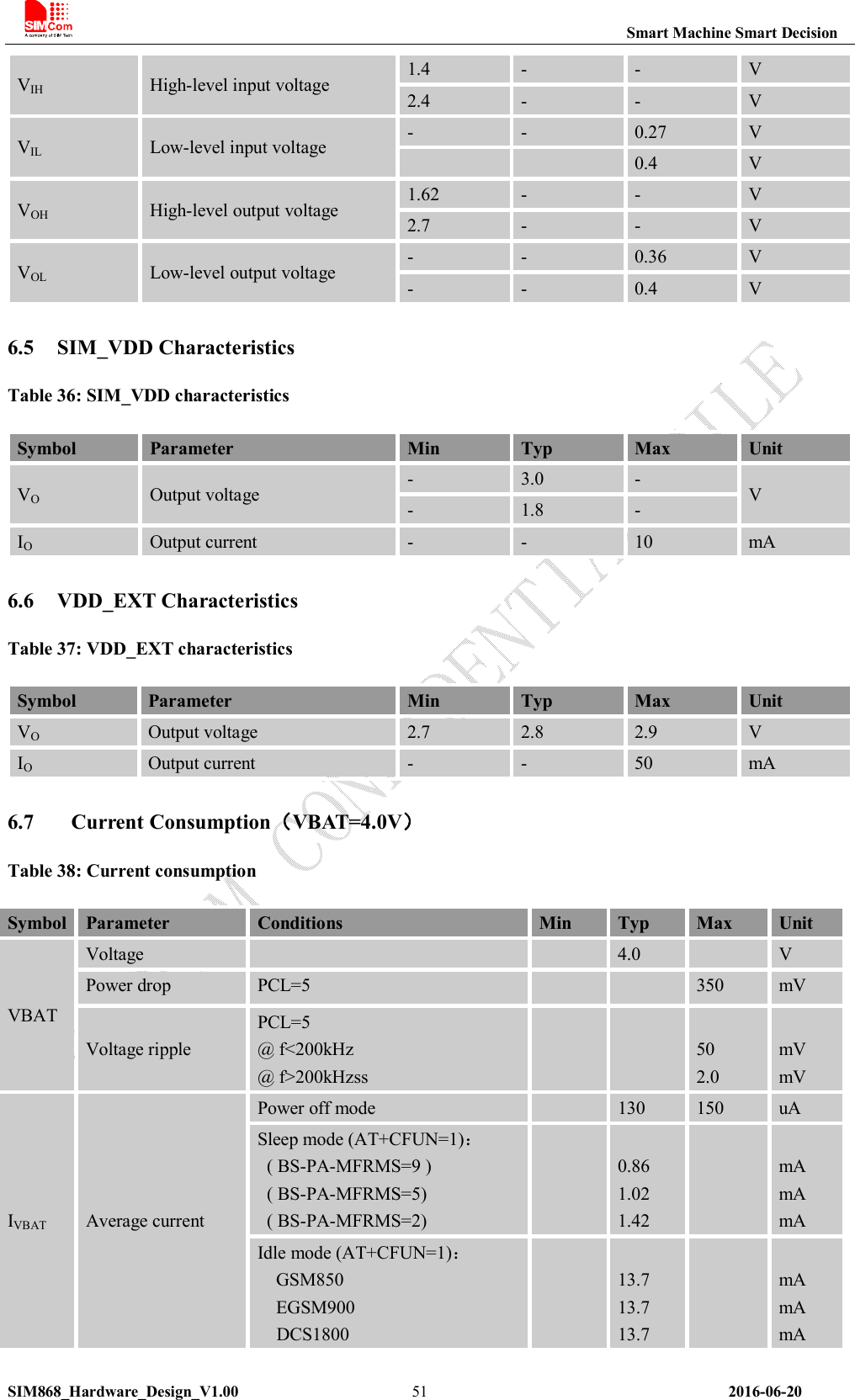
Simcom 201607 GSM/GPRS+GPS module User Manual UDV 201607 SIM868 REV2 4
Shanghai Simcom Ltd. GSM/GPRS+GPS module UDV 201607 SIM868 REV2 4
UserManual.wiki
>
Simcom
>
201607 User Manual
UDV-201607 SIM868_User Manual_REV2-4
Navigation menu
Upload a User Manual
Namespaces
Wiki Guide
HTML
PDF
Info
Views
User Manual
Discussion / Help
Navigation
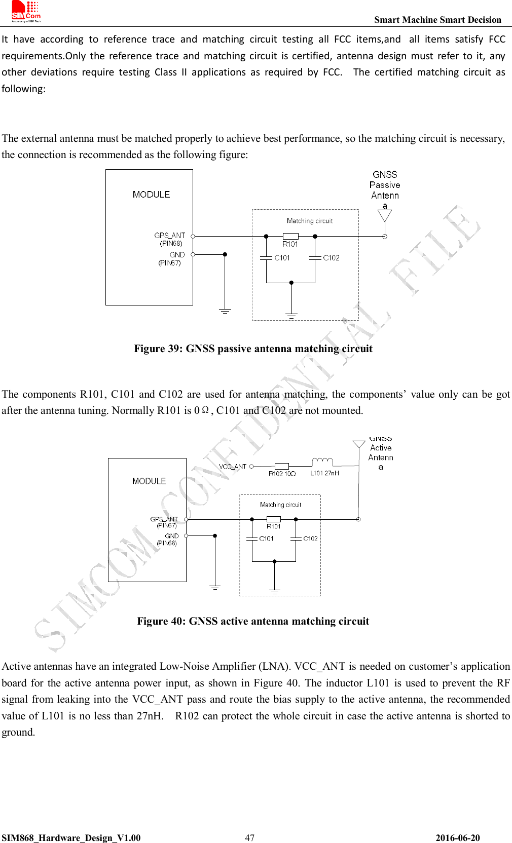
![Smart Machine Smart Decision SIM868_Hardware_Design_V1.00 10 2016-06-20 1. Introduction This document describes SIM868 hardware interface in great detail. The document can help customer to quickly understand SIM868 interface specifications, electrical and mechanical details. With the help of this document and other SIM868 application notes, customer guide, customers can use SIM868 to design various applications quickly. 2. SIM868 Overview Designed for global market, SIM868 is integrated with a high performance GSM/GPRS engine and a GNSS engine. SIM868 is a quad-band GSM/GPRS module that works on frequencies GSM 850MHz, EGSM 900MHz, DCS 1800MHz and PCS 1900MHz. SIM868 features GPRS multi-slot class 12/class 10 (optional) and supports the GPRS coding schemes CS-1, CS-2, CS-3 and CS-4. The GNSS solution offers best-in-class acquisition and tracing sensitivity, Time-To-First-Fix (TTFF) and accuracy. With a tiny configuration of 17.6*15.7*2.3mm, SIM868 can meet almost all the space requirements in customers’ applications, such as smart phone, PDA and other mobile devices. SIM868 is a SMT+LGA package with 77 pads, and provides all hardware interfaces between the module and customers’ boards. One 3 lines serial port and one full modem serial port; USB interface which can be used for debugging and upgrading firmware; Audio channels which include a microphone input and two speakers output; Programmable general purpose input and output; Two SIM cards interface; Support GNSS function; SD card interface; I2C interface; ADC interface. SIM868 is designed with power saving technique so that the current consumption is as low as 0.65 mA in sleep mode (with GNSS engine powered down). SIM868 integrates TCP/IP protocol and extended TCP/IP AT commands which are very useful for data transfer applications. For details about TCP/IP applications, please refer to document [2]. 2.1. SIM868 Table 1: Module Information Information SIM868 GSM 850,900,1800 and 1900MHz GNSS GNSS interface FLASH 32Mbit RAM 32Mbit 2.2. SIM868 Key Features Table 2: SIM868 Key Features](https://usermanual.wiki/Simcom/201607/User-Guide-3089201-Page-10.png)
![Smart Machine Smart Decision SIM868_Hardware_Design_V1.00 11 2016-06-20 Feature Implementation Power supply 3.4V ~4.2V Power saving Typical power consumption in sleep mode is 0.65 mA (AT+CFUN=0 ) Frequency bands Quad-band: GSM 850, EGSM 900, DCS 1800, PCS 1900. SIM868 can search the 4 frequency bands automatically. The frequency bands can also be set by AT command “AT+CBAND”. For details, please refer to document [1]. Compliant to GSM Phase 2/2+ Transmitting power Class 4 (2W) at GSM 850 and EGSM 900 Class 1 (1W) at DCS 1800 and PCS 1900 GPRS connectivity GPRS multi-slot class 12(default) GPRS multi-slot class 1~12 (option) Temperature range Normal operation: -40°C ~ +85°C Storage temperature -45°C ~ +90°C Data GPRS GPRS data downlink transfer: max. 85.6 kbps GPRS data uplink transfer: max. 85.6 kbps Coding scheme: CS-1, CS-2, CS-3 and CS-4 PAP protocol for PPP connect Integrate the TCP/IP protocol. Support Packet Broadcast Control Channel (PBCCH) USSD Unstructured Supplementary Services Data (USSD) support SMS MT, MO, CB, Text and PDU mode SMS storage: SIM card SIM interface Support SIM card: 1.8V, 3V External antenna Antenna pad Audio features Speech codec modes: Half Rate (ETS 06.20) Full Rate (ETS 06.10) Enhanced Full Rate (ETS 06.50 / 06.60 / 06.80) Adaptive multi rate (AMR) Echo Cancellation Noise Suppression Serial port and USB port Serial port: Default one Full modem serial port Can be used for AT commands or data stream Support RTS/CTS hardware handshake and software ON/OFF flow control Multiplex ability according to GSM 07.10 Multiplexer Protocol Autobauding supports baud rate from 1200 bps to 115200bps upgrading firmware USB port: Can be used for debugging and upgrading firmware Phonebook management Support phonebook types: SM, FD, LD, RC, ON, MC SIM application toolkit GSM 11.14 Release 99 Physical characteristics Size:17.6*15.7*2.3mm Weight:1.5g Firmware upgrade Full modern serial port or USB interface (recommend to use USB port)](https://usermanual.wiki/Simcom/201607/User-Guide-3089201-Page-11.png)
![Smart Machine Smart Decision SIM868_Hardware_Design_V1.00 22 2016-06-20 Note: Hardware power off voltage is 3.0V. 4.1.2. Monitoring Power Supply AT command “AT+CBC” can be used to monitor the VBAT voltage. For detail, please refer to document [1]. 4.2. Power on/off SIM868 4.2.1. Power on SIM868 Customer can power on SIM868 by pulling down the PWRKEY pin for at least 1 second and release. This pin is already pulled up to 3V in the module internal, so external pull up is not necessary. Reference circuits are shown as below. 4.7K47KTurn on/off impulsePWRKEY Power on/off logic100K3VModule1K Figure 10: Powered on/down module using transistor PWRKEY Power on/off logic100K3VModule1K Figure 11: Powered on/down module using button The power on timing is illustrated as in the following figure. Figure 12: Timing of power on module](https://usermanual.wiki/Simcom/201607/User-Guide-3089201-Page-22.png)
![Smart Machine Smart Decision SIM868_Hardware_Design_V1.00 23 2016-06-20 When power on procedure is completed, SIM868 will send following URC to indicate that the module is ready to operate at fixed baud rate. RDY This URC does not appear when autobauding function is active. Note: Customer can use AT command “AT+IPR=x” to set a fixed baud rate and save the configuration to non-volatile flash memory. After the configuration is saved as fixed baud rate, the Code “RDY” should be received from the serial port every time when SIM868 is powered on. For details, please refer to the chapter “AT+IPR” in document [1]. 4.2.2. Power off SIM868 SIM868 will be powered off in the following situations: Normal power off procedure: power off SIM868 by the PWRKEY pin. Normal power off procedure: power off SIM868 by AT command “AT+CPOWD=1”. Abnormal power off: over-voltage or under-voltage automatic power off. Abnormal power off: over-temperature or under-temperature automatic power off. 4.2.2.1. Power off SIM868 by the PWRKEY Pin Customer can power off SIM868 by pulling down the PWRKEY pin for at least 1 second and release. Please refer to the power on circuit. The power off timing is illustrated in the following figure. Figure 13: Timing of power off SIM868 by PWRKEY Note: 1. the module will restart after pull down the pwrkey over 33 seconds. 2. VDD_EXT will power off after STATUS change into low level and the PWRKEY release 55ms.. If 1s<T1<2s,T2>2s; If 2s≤T1<33s,T2>T1+55ms This procedure makes the module log off from the network and allows the software to enter into a secure state to save data before completely shut down. Before the completion of the power off procedure, the module will send URC: NORMAL POWER OFF At this moment, AT commands can’t be executed any more. Power off mode can also be indicated by STATUS pin, which is at low level at this time.](https://usermanual.wiki/Simcom/201607/User-Guide-3089201-Page-23.png)
![Smart Machine Smart Decision SIM868_Hardware_Design_V1.00 24 2016-06-20 4.2.2.2. Power off SIM868 by AT Command SIM868 can be powered off by AT command “AT+CPOWD=1”. This procedure makes the module log off from the network and allows the software to enter into a secure state to save data before completely shut down. Before the completion of the power off procedure, the module will send URC: NORMAL POWER OFF At this moment, AT commands can’t be executed any more. Power off mode can also be indicated by STATUS pin, which is at low level at this time. For detail about AT command “AT+CPOWD”, please refer to document [1]. 4.2.2.3. Over-Temperature or Under-Temperature Power off The module will constantly monitor the temperature of the module, If the temperature ≥ +80℃, the following URC will be reported: +CMTE: 1 If the temperature ≤ -30℃, the following URC will be reported: +CMTE:-1 If the temperature > +85℃, the following URC will be reported, and the module will be automatically powered off. +CMTE: 2 If the temperature < -40℃, the following URC will be reported, and the module will be automatically powered off. +CMTE:-2 At this moment, AT commands can’t be executed any more. Power off mode can also be indicated by STATUS pin, which is at low level at this time. Note:The default temperature detect is disable, AT command “AT+CMTE” could be used to read the temperature when the module is running.For details please refer to document [1]. 4.2.2.4. Restart SIM868 by PWRKEY Pin: When the module works normally, if the customer wants to restart the module, follow the procedure below: 1) Power off the module. 2) Wait for at least 800ms after STATUS pin changed to low level. 3) Power on the module. Figure 14: Timing of restart SIM868](https://usermanual.wiki/Simcom/201607/User-Guide-3089201-Page-24.png)
![Smart Machine Smart Decision SIM868_Hardware_Design_V1.00 25 2016-06-20 4.3. Power Saving Mode SIM868 has two power saving modes: Minimum functionality mode and sleep mode. AT command “AT+CSCLK=1”can be used to set SIM868 into sleep mode. AT command “AT+CFUN=<fun>“can be used to set SIM868 into minimum functionality. When SIM868 is in sleep mode and minimum functionality mode, the current of module is lowest. 4.3.1. Minimum Functionality Mode There are three functionality modes, which could be set by AT command “AT+CFUN=<fun>“. The command provides the choice of the functionality levels <fun>=0, 1, 4. AT+CFUN=0: Minimum functionality. AT+CFUN=1: Full functionality (default). AT+CFUN=4: Flight mode (disable RF function). Table 8: The current consumption of Function Mode <fun> BS-PA-MFRMS Current consumption(mA) 0 / 0.65 1 9 0.86 5 1.02 2 1.42 4 / 0.69 Minimum functionality mode minimizes the current consumption to the lowest level. If SIM868 is set to minimum functionality by “AT+CFUN=0”, the RF function and SIM card function will be disabled. In this case, the serial port is still accessible, but partial AT commands and correlative to RF function and SIM card function will not be accessible. For detailed information about AT command “AT+CFUN=<fun>“, please refer to document [1]. 4.3.2. Sleep Mode 1 (AT+CSCLK=1) Customer can control SIM868 module to enter or exit the sleep mode (AT+CSCLK=1) by DTR signal. When DTR is in high level and without interrupt (on air and hardware such as GPIO interrupt or data in serial port), SIM868 will enter sleep mode automatically. In this mode, SIM868 can still receive paging or SMS from network but the serial port is not accessible. 4.3.3. Wake Up SIM868 from Sleep Mode 1 When SIM868 is in sleep mode 1(AT+CSCLK=1), the following methods can wake up the module: Pull down DTR pin. The serial port will be active after DTR pin is pulled to low level for about 50ms. Receive a voice or data call from network. Receive a SMS from network. Receive external interrupt. Note: After module has received incoming call or new SMS, serial port can report URC, but the serial port can not input AT command. Only after the DTR pin is pulled to low level for 50ms, the serial port can input AT](https://usermanual.wiki/Simcom/201607/User-Guide-3089201-Page-25.png)
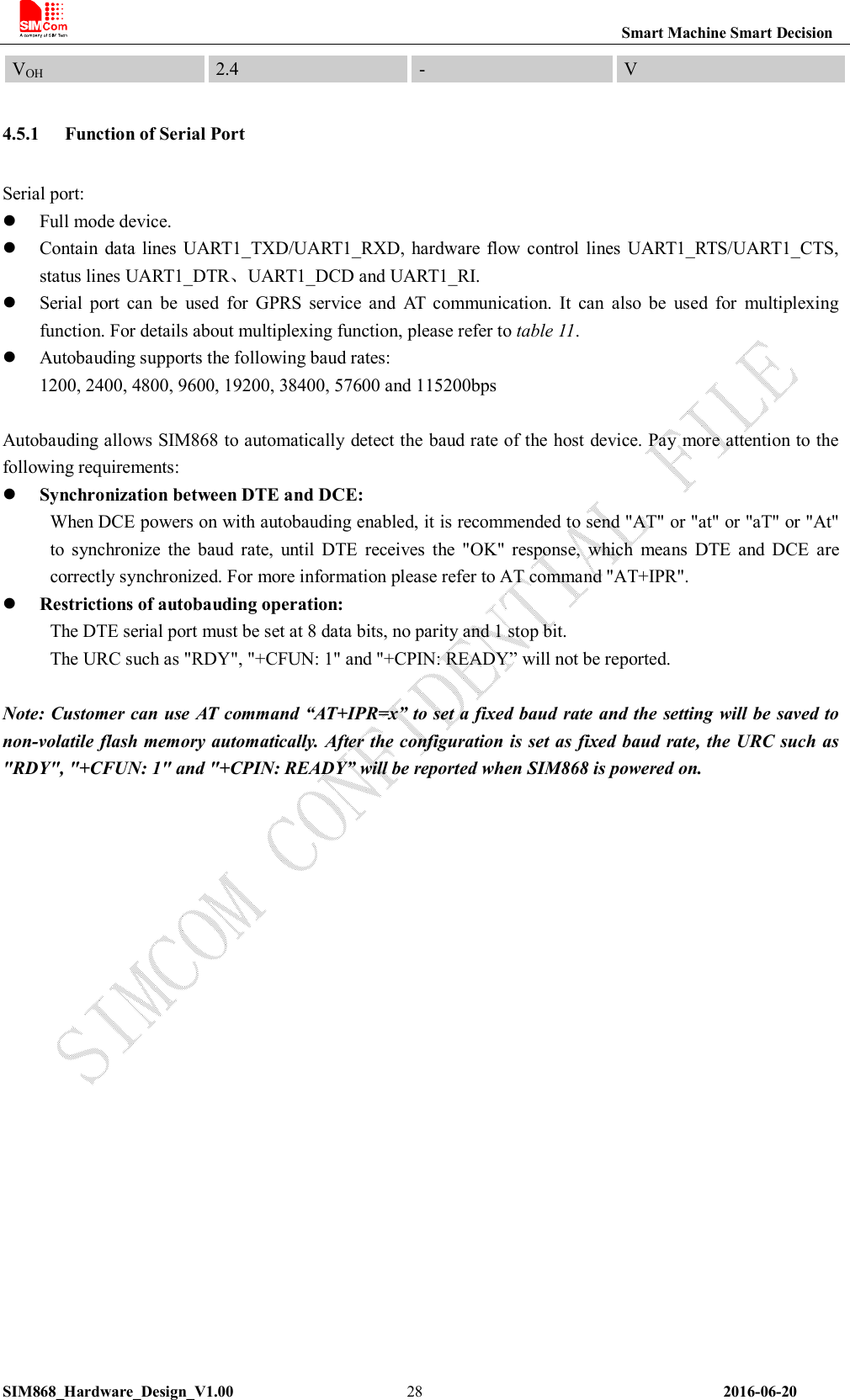
![Smart Machine Smart Decision SIM868_Hardware_Design_V1.00 27 2016-06-20 Rechargeable battery backup Figure 17: RTC supply from rechargeable battery 4.5. Serial Port and USB Interface SIM868 default provides one unbalanced asynchronous serial ports. The module is designed as a DCE (Data Communication Equipment). The following figure shows the connection between module and client (DTE). Table 9: Serial port and USB pin definition Note: Hardware flow control is disabled by default. AT command “AT+IFC=2, 2”can enable hardware flow control. AT command “AT+IFC=0,0”can disable hardware flow control. For more details please refer to document [1]. Table 10: Serial port characteristics Symbol Min Max Unit VIL -0.3 0.7 V VIH 2.1 3.1 V VOL - 0.4 V Pin name Pin number Function Serial port UART1_DTR 6 Data terminal ready UART1_RI 7 Ring indicator UART1_DCD 5 Data carrier detect UART1_CTS 4 Clear to send UART1_RTS 3 Request to send UART1_TXD 1 Transmit data UART1_RXD 2 Receive data UART2_TXD 22 Transmit data UART2_RXD 23 Receive data GPS_TXD 61 Transmit data GPS_RXD 62 Receive data Debug port USB_VBUS 24 USB power supply USB_DP 25 D+ data input/output USB_DM 26 D- data input/output](https://usermanual.wiki/Simcom/201607/User-Guide-3089201-Page-27.png)
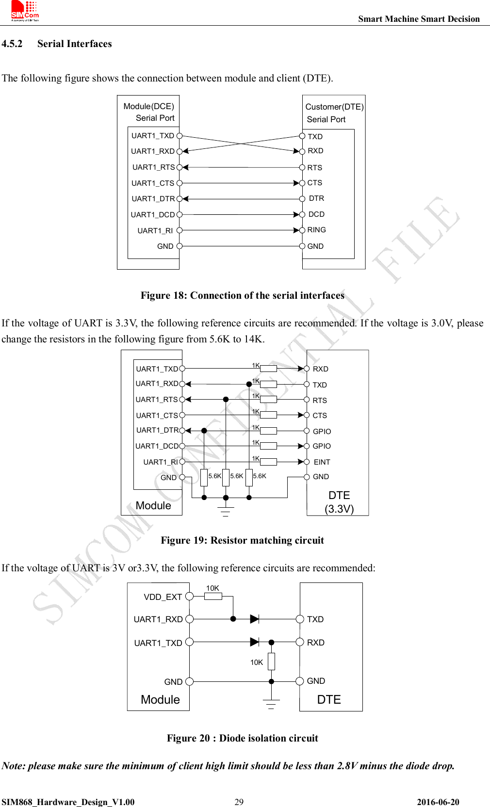
![Smart Machine Smart Decision SIM868_Hardware_Design_V1.00 31 2016-06-20 Note: please reserve the USB interface or test point for the further debugging Table 11: USB_VBUS operation voltage Pin Min Typ Max Unit USB_VBUS 4.3 5.0 7.0 V 4.5.4 Software Upgrade Customer could upgrade module’s firmware through USB or UART interface. If upgrading through USB interface, it is necessary to power on SIM868 first, and then connect USB_VBUS, USB_DP, USB_DM, and GND to PC. There is no need to operate PWRKEY pin in the whole procedure, when SIM868 detects USB_VBUS and could communicate normally with USB_DP and USB_DM, it will enter USB download mode automatically. If customer upgrades the software through UART interface, it is strongly recommended to lead the UART1_TXD, UART1_RXD, GND and PWRKEY pin to IO connector for the upgrading, and PWRKEY pin should connect to GND while upgrading. Refer to the following figure for debugging and upgrading software. UART1_TXDModule(DCE)UART1_RXDGNDPWRKEYTXDRXDGNDSerial PortPWRKEYI/O Connector Figure 24: Connection for software upgrading and debugging The UART interface supports the CMOS level. If customer connects the module to the computer, the level shifter should be added between the DCE and DTE. 4.6. UART1_RI Behaviors Table 12: RI behaviors State RI response Standby High Voice call The pin is changed to low. When any of the following events occur, the pin will be changed to high: (1)Establish the call (2)Hang up the call SMS The pin is changed to low, and kept low for 120ms when a SMS is received. Then it is changed to high. Others For more details, please refer to document [2].](https://usermanual.wiki/Simcom/201607/User-Guide-3089201-Page-31.png)
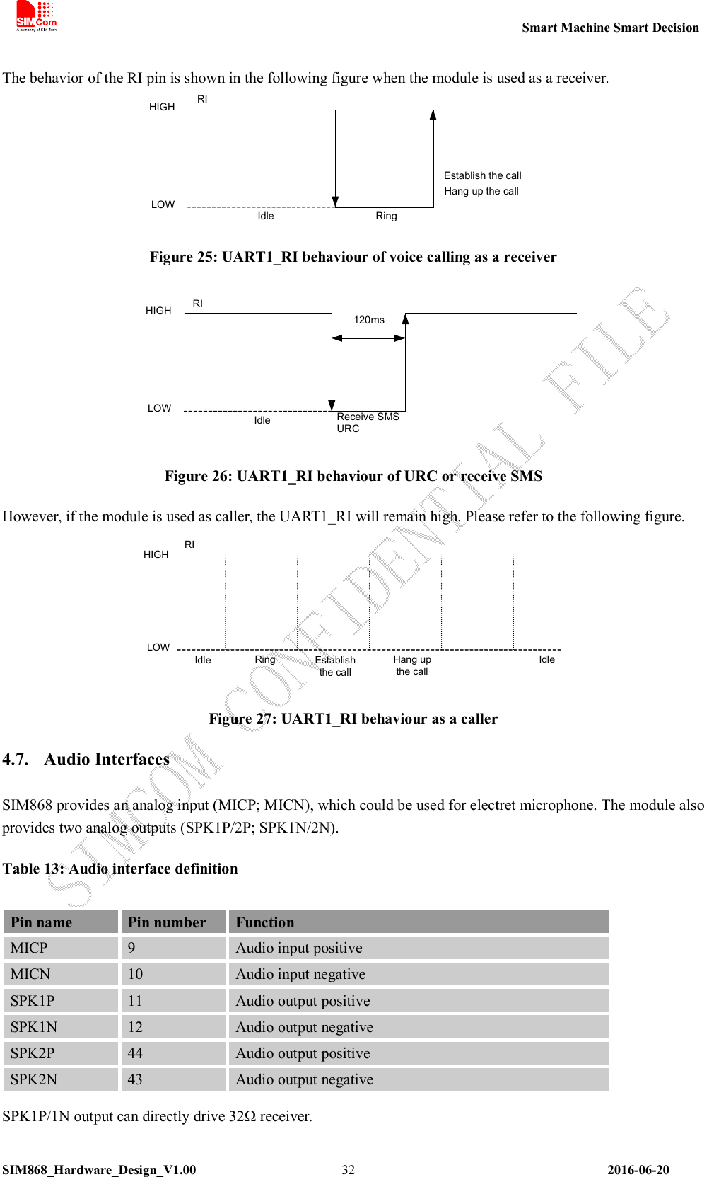
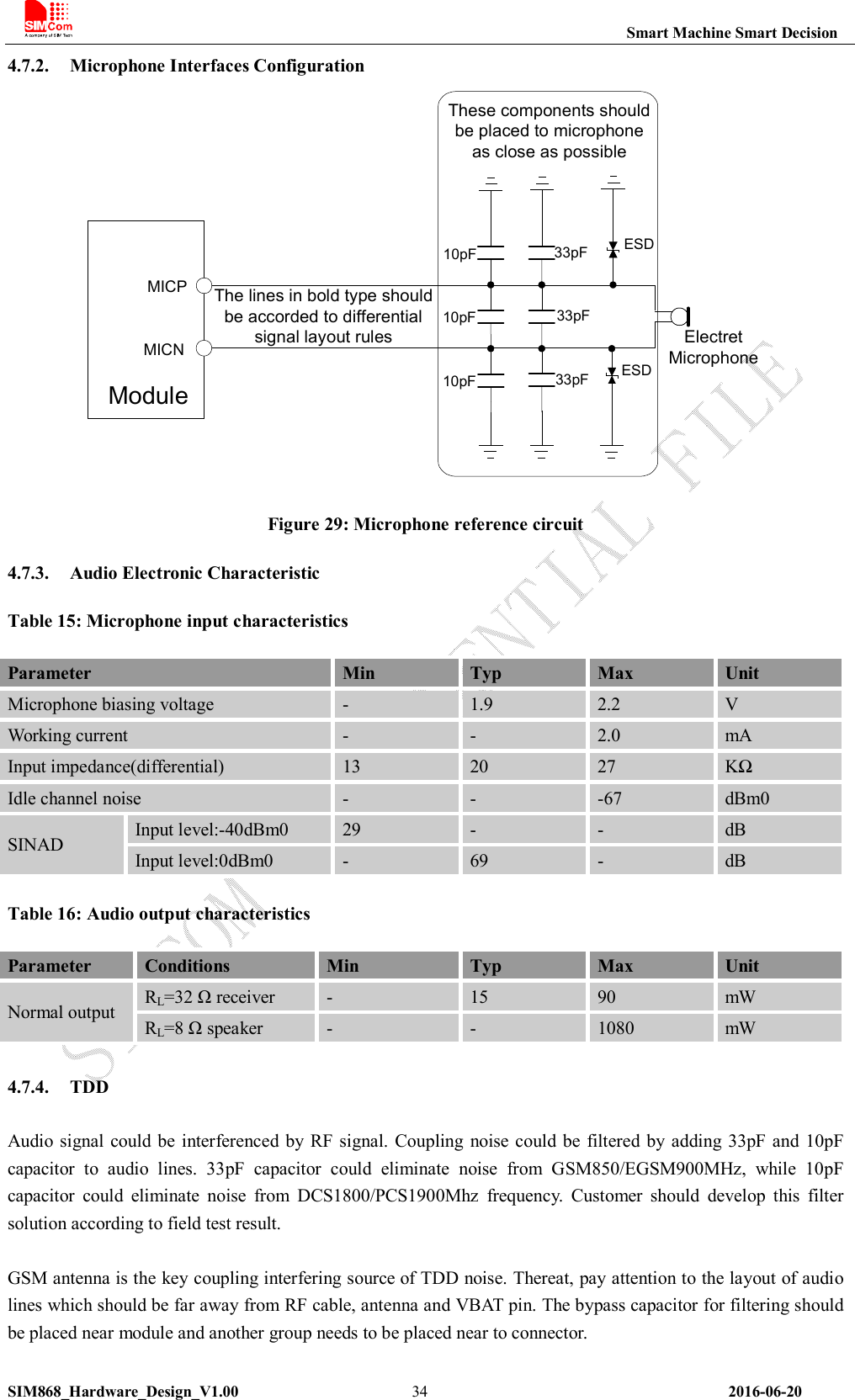
![Smart Machine Smart Decision SIM868_Hardware_Design_V1.00 33 2016-06-20 SIM868 internal has class-AB audio amplifier, the following table is class-AB performance: Table 14: Performance of audio amplifier Test Conditions Class-AB AMP 4.2V 8Ω THD+N=1% 0.87W 3.3V 8Ω THD+N=1% 0.53W 4.2V 8Ω THD+N=10% 1.08W 3.3V 8Ω THD+N=10% 0.65W SPK2P/2N output can directly drive 8Ω speaker. AT command “AT+CMIC” is used to adjust the input gain level of microphone. AT command “AT+SIDET” is used to set the side-tone level. In addition, AT command “AT+CLVL” is used to adjust the output gain level. For more details, please refer to document [1]. In order to improve audio performance, the following reference circuits are recommended. The audio signals have to be layout according to differential signal layout rules as shown in following figures. 4.7.1. Speaker Interfaces Configuration SPK1P/2PClose to speakerESDESD10pF33pF33pF33pFModuleSPK1N/2N10pF10pF10pF33pF33pF33pF10pF10pF Figure 28: Speaker reference circuit](https://usermanual.wiki/Simcom/201607/User-Guide-3089201-Page-33.png)
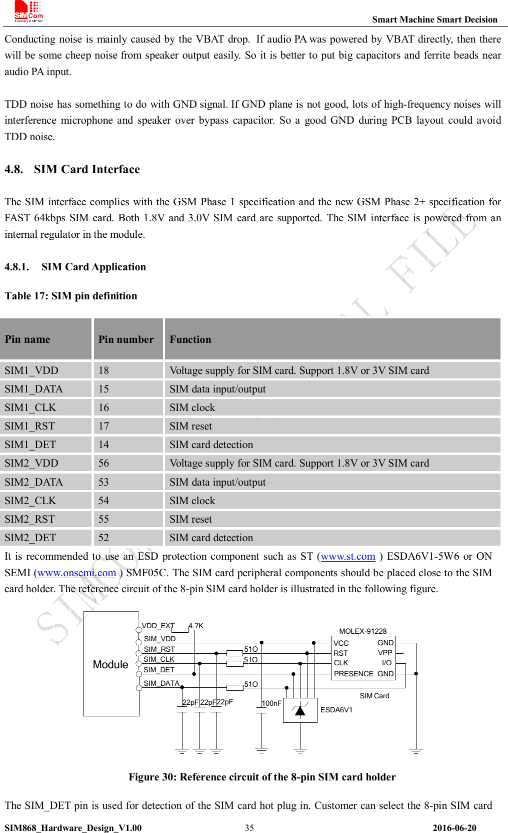
![Smart Machine Smart Decision SIM868_Hardware_Design_V1.00 36 2016-06-20 holder to implement SIM card detection function. AT command “AT+CSDT” is used to enable or disable SIM card detection function. For details of this AT command, please refer to document [1]. If the SIM card detection function is not used, customer can keep the SIM_DET pin open. The reference circuit of 6-pin SIM card holder is illustrated in the following figure. Module100nFMOLEX-91228C107 10M 006 51222pFVCC GNDRST VPPCLK I/OSIM_VDDSIM_RSTSIM_CLKSIM_DATAESDA6V1SIM_DET51O51O22pF51O22pF Figure 31: Reference circuit of the 6-pin SIM card holder 4.8.2. SIM Card Design Guide SIM card signal could be interferenced by some high frequency signal, it is strongly recommended to follow these guidelines while designing: SIM card holder should be far away from GSM antenna SIM traces should keep away from RF lines, VBAT and high-speed signal lines The traces should be as short as possible Keep SIM card holder’s GND connect to main ground directly Shielding the SIM card signal by ground well Recommended to place a 100nF capacitor on SIM_VDD line and keep close to the SIM card holder Add some TVS which parasitic capacitance should not exceed 50pF Add 51Ω resistor to (SIM_RST/SIM_CLK/SIM_DATA) signal could enhance ESD protection Add 22pf capacitors to (SIM_RST/SIM_CLK/SIM_DATA) signal to reduce RF interference](https://usermanual.wiki/Simcom/201607/User-Guide-3089201-Page-36.png)
![Smart Machine Smart Decision SIM868_Hardware_Design_V1.00 39 2016-06-20 4.9. SD Interface SD interface can be configured as PCM interface; the following table shows the detailed multiplexing function. Table 20: SD multiplexing function Pin name Pin number Mode 0(default) Mode 1 Mode 2 Mode 3 MCCA3 46 MCCA3 DAIPCMOUT(1.8V) GPIO EINT19 MCCA2 47 MCCA2 DAICLK(1.8v) GPIO EINT18 MCCA1 48 MCCA1 DAIPCMIN(1.8v) GPIO EINT17 MCCA0 49 MCCA0 DAISYNC (1.8v) GPIO MCCK 50 MCCK GPIO MCCM0 51 MCCM0 GPIO Note: Customer can use AT command set mode. For detail, please refer to document [1]. SIM868 provides a hardware SD interface: Figure 34: SD reference circuit If power supply is 2.8V for SD card, customer can use VDD_EXT; if power supply is 3.3V, please use external design LDO. 4.10. I2C Bus The SIM868 provides an I2C interface which is only used in the embedded AT application. Table 21: Pin definition of the I2C Note: 1. I2C should be pulled up to 2.8V via 4.7K externally. 2. I2C function is not supported in the standard firmware. If you need, please contact SIMCom. 4.10.1. I2C Multiplexing Function Table 22: I2C multiplexing function Pin name Pin number Description SCL 65 I2C serial bus clock(open drain output) SDA 64 I2C serial bus data(open drain output)](https://usermanual.wiki/Simcom/201607/User-Guide-3089201-Page-39.png)
![Smart Machine Smart Decision SIM868_Hardware_Design_V1.00 40 2016-06-20 Pin name Pin number Mode 0(default) Mode 1 SCL 65 SCL GPIO SDA 64 SDA GPIO Note: Customer can use AT command set mode. For detail, please refer to document t[1]. 4.11. ADC Table 23: Pin definition of the ADC SIM868 provides an auxiliary ADC, which can be used to measure the voltage. Customer can use AT command “AT+CADC” to read the voltage value. Note: Customer can use AT command set mode. For detail, please refer to document t[1]. Table 24: ADC specification Parameter Min Typ Max Unit Voltage range 0 - 2.8 V ADC Resolution - 10 - bits RIN Input resistance Unselected channel Selected channel 400 1 M M CIN Input capacitance Unselected channel Selected channel 50 4 fF pF Sampling rate - - 1.08 MHz ADC precision 10 30 mV 4.12. Network Status Indication Table 25: Pin definition of the NETLIGHT The NETLIGHT pin can be used to drive a network status indication LED. The status of this pin is listed in following table: Table 26: Status of the NETLIGHT pin Status SIM868 behavior Off Powered off 64ms On/ 800ms Off Not registered the network 64ms On/ 3000ms Off Registered to the network 64ms On/ 300ms Off GPRS communication is established Pin name Pin number Description ADC 38 Analog voltage input Pin name Pin number Description NETLIGHT 41 Network Status Indication](https://usermanual.wiki/Simcom/201607/User-Guide-3089201-Page-40.png)
![Smart Machine Smart Decision SIM868_Hardware_Design_V1.00 41 2016-06-20 Reference circuit is recommended in the following figure: ModuleNETLIGHTVBAT4.7K47KR Figure 35: Reference circuit of NETLIGHT Table 27: NETLIGHT multiplexing function Pin name Pin number Mode 0(default) Mode 1 NETLIGHT 41 NETLIGHT GPIO Note: Customer can use AT command set mode. For detail, please refer to document t[1]. 4.13. Operating Status Indication The pin42 is for operating status indication of the module. The pin output is high when module is powered on, and output is low when module is powered off. Table 28: Pin definition of the STATUS Pin name Pin number Description STATUS 42 Operating status indication Note: For timing about STATUS, please reference to the chapter “4.2 power on/down scenarios” 4.14. RF Synchronization Signal The synchronization signal serves to indicate growing power consumption during the transmit burst. Table 29: Definition of the RF_SYNC pin The timing of the synchronization signal is shown in the following figure. High level of the RF_SYNC signal indicates increased power consumption during transmission. Pin name Pin number Description RF_SYNC 29 Transmit synchronization signal](https://usermanual.wiki/Simcom/201607/User-Guide-3089201-Page-41.png)
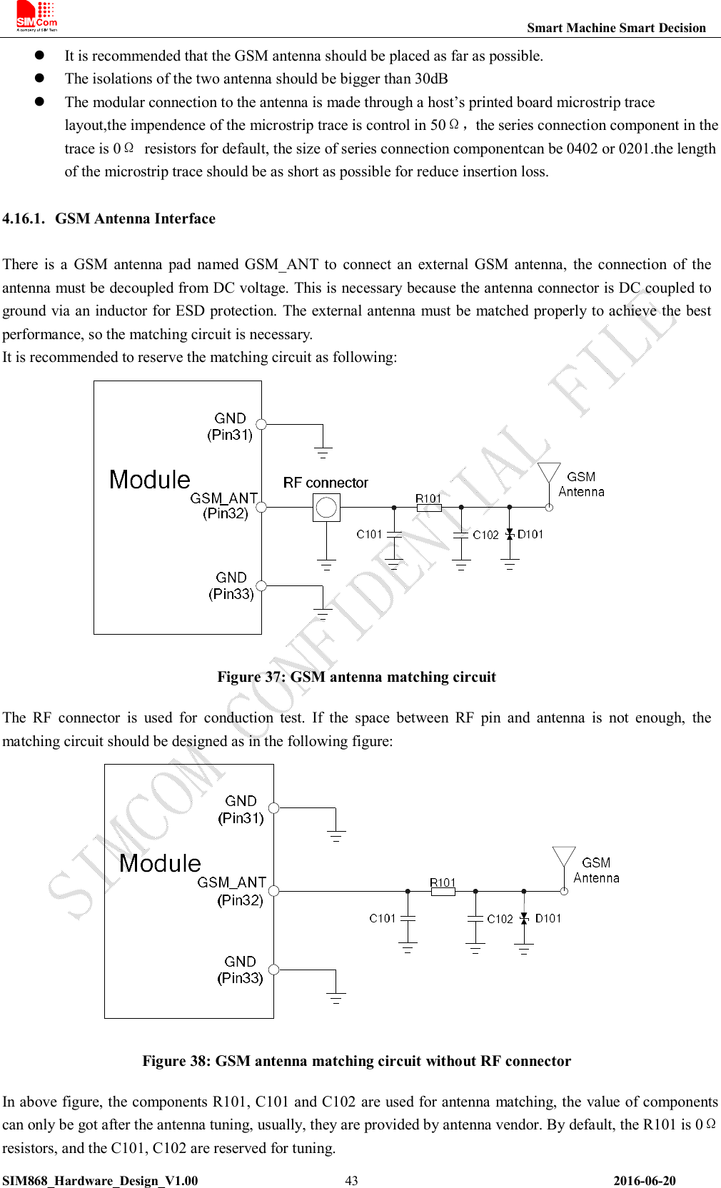
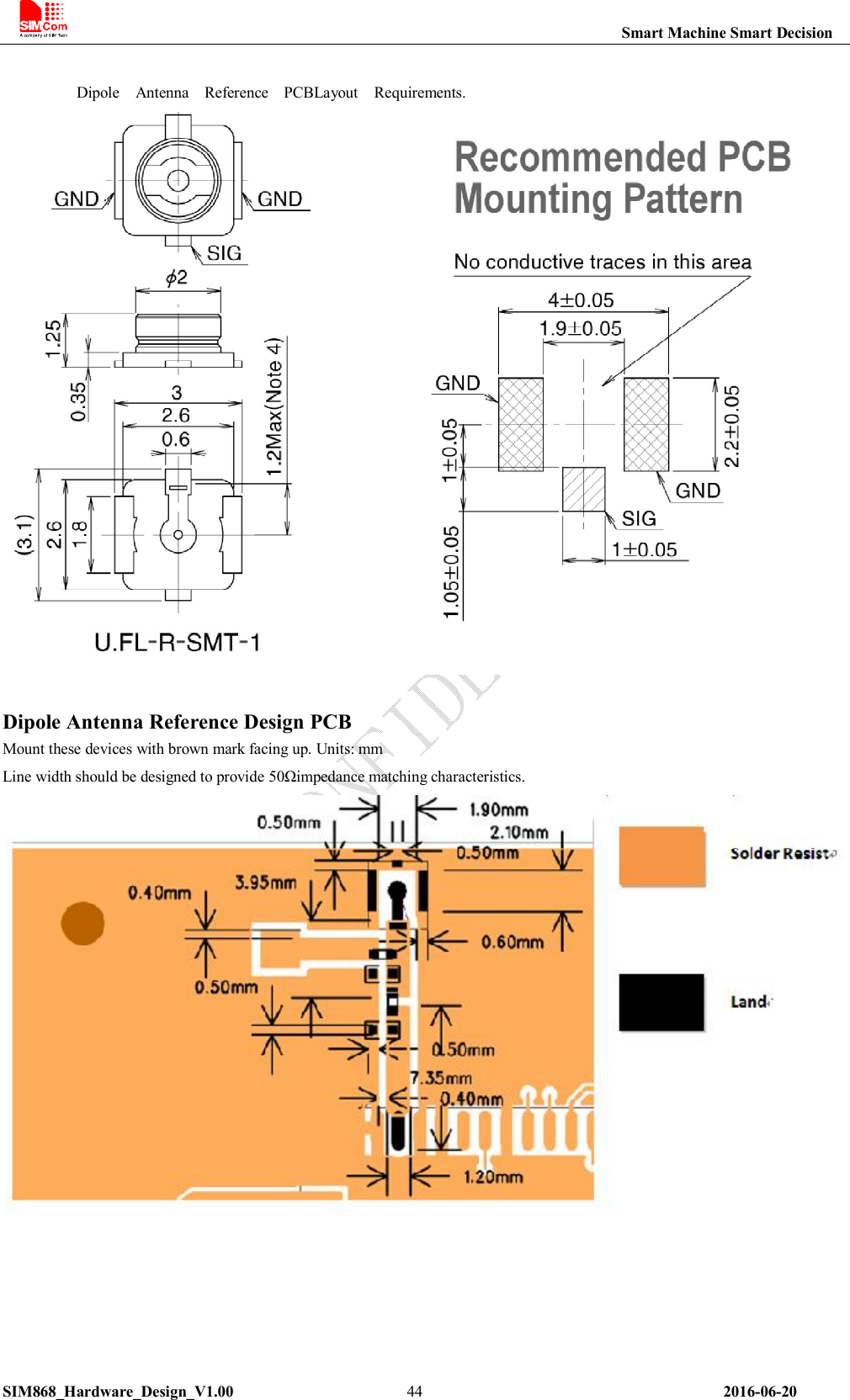
![Smart Machine Smart Decision SIM868_Hardware_Design_V1.00 42 2016-06-20 Transmit burstRF_SYNC577us220us Figure 36: RF_SYNC signal during transmit burst 4.14.1. RF_SYNC Multiplexing Function RF_SYNC can also be used as GPIO to indicate the RF Jamming. The RF_SYNC function and RF Jamming Detection function can be switched by AT+SJDR command. Table 30: RF_SYNC Multiplexing function Pin name Pin number Mode 0(default) Mode 1 RF_SYNC 29 RF Synchronization Signal JD(RF jamming detection) Note: About AT+SJDR, please refer to document [1]. 4.15. GNSS 4.15.1. GNSS Overview SIM868 provide a high-performance L1 GNSS solution for cellular handset applications. The solution offers best-in-class acquisition and tracking sensitivity, Time-To-First-Fix (TTFF) and accuracy. The GNSS engine supports both fully-autonomous operations for use in handheld consumer navigation devices and other standalone navigation systems. GNSS engine Performance, please refer to Table 3. GNSS NMEA information is output by serial port. The default baud rate is 115200bps. 4.15.2. Power on/down GNSS The GNSS engine is controlled by GNSS_EN PIN, so when it is necessary to run GNSS,the GNSS_EN must be pulled up to 2.8V. When it is necessary to power off GNSS,the GNSS_EN must be pulled down to GND. 4.15.3. 1PPS Output The 1PPS pin outputs pulse-per-second (1PPS) pulse signal for precise timing purposes. It will come out after successfully positioning .The 1PPS signal can be provided through designated output pin for many external applications. 4.16. Antenna Interface There are two antenna interfaces, GSM_ANT、GPS_ANT. The input impendence of the two antenna should be 50Ω, and the VSWR should be less than 2.](https://usermanual.wiki/Simcom/201607/User-Guide-3089201-Page-42.png)
![Smart Machine Smart Decision SIM868_Hardware_Design_V1.00 57 2016-06-20 8. Appendix I. Related Documents Table 46: Related documents SN Document name Remark [1] SIM800_Series_AT_Command_Manual [2] SIM800 Series Port Application Note_V1 02.doc [3] ITU-T Draft new recommendation V.25ter: Serial asynchronous automatic dialing and control [4] GSM 07.07: Digital cellular telecommunications (Phase 2+); AT command set for GSM Mobile Equipment (ME) [5] GSM 07.10: Support GSM 07.10 multiplexing protocol [6] GSM 07.05: Digital cellular telecommunications (Phase 2+); Use of Data Terminal Equipment – Data Circuit terminating Equipment (DTE – DCE) interface for Short Message Service (SMS) and Cell Broadcast Service (CBS) [7] GSM 11.14: Digital cellular telecommunications system (Phase 2+); Specification of the SIM Application Toolkit for the Subscriber Identity Module – Mobile Equipment (SIM – ME) interface [8] GSM 11.11: Digital cellular telecommunications system (Phase 2+); Specification of the Subscriber Identity Module – Mobile Equipment (SIM – ME) interface [9] GSM 03.38: Digital cellular telecommunications system (Phase 2+); Alphabets and language-specific information [10] GSM 11.10 Digital cellular telecommunications system (Phase 2); Mobile Station (MS) conformance specification; Part 1: Conformance specification [11] AN_Serial Port AN_Serial Port [12] SIM868_GNSS_Application Note](https://usermanual.wiki/Simcom/201607/User-Guide-3089201-Page-57.png)