Simcom SIM800C GSM/GPRS Module User Manual UDV SIM800C Rev 3
Shanghai Simcom Ltd. GSM/GPRS Module UDV SIM800C Rev 3
Simcom >
UDV-SIM800C User Manual_Rev 3
SIM800C_User Manual_
V1.00

SIM900-DS Document
- 2 -
Compliance Information
FCC Compliance Statement: This device complies with Part 15 of the FCC Rules . Operation is subject to the
following two conditions: 1. This device may not cause harmful interference, and 2. This device must accept
any interference received, including interference that may cause undesired operation. This device must accept
any interference received, including interference that may cause undesired operation. Product that is a radio
transmitter is labeled with FCC ID.
FCC Caution
(1) Exposure to Radio Frequency Radiation. This equipment must be installed and operated in accordance with
provided instructions and the antenna(s) used for this transmitter must be installed to provide a separation
distance of at least 20 cm from all persons and must not be collocated or operating in conjunction with any other
antenna or transmitter. End-users and installers must be provided with antenna installation instructions and
transmitter operating conditions for satisfying RF exposure compliance.
(2) Any changes or modifications not expressly approved by the grantee of this device could void the user's
authority to operate the equipment.
(3) This Transmitter must not be co-located or operating in conjunction with any other antenna or transmitter.
(4) Changes or modifications to this unit not expressly approved by the party responsible for compliance could
void the user authority to operate the equipment.
(5) The modules FCC ID is not visible when installed in the host, or
(6) If the host is marketed so that end users do not have straight forward commonly used methods for access to
remove the module so that the FCC ID of the module is visible; then an additional permanent label referring to
the enclosed module: Contains Transmitter Module FCC ID: UDV-SIM800C or Contains FCC ID:
UDV-SIM800C must be used.
General Notes
SIMCom offers this information as a service to its customers, to support application and engineering efforts that
use the products designed by SIMCom. The information provided is based upon requirements specifically
provided to SIMCom by the customers. SIMCom has not undertaken any independent search for additional
relevant information, including any information that may be in the customer’s possession. Furthermore, system
validation of this product designed by SIMCom within a larger electronic system remains the responsibility of
the customer or the customer’s system integrator. All specifications supplied herein are subject to change.
Copyright
This document contains proprietary technical information which is the property of Shanghai SIMCom Wireless
Solutions Ltd, copying of this document and giving it to others and the using or communication of the contents
thereof, are forbidden without express authority. Offenders are liable to the payment of damages. All rights
reserved in the event of grant of a patent or the registration of a utility model or design. All specification
supplied herein are subject to change without notice at any time.
Copyright © Shanghai SIMCom Wireless Solutions Ltd. 2014.
Smart Machine Smart Decision
- 3 -
1. SIM800C Description
1.1. Summarize
SIM800C designed by SIMCom is a quad band module which supports GSM/GPRS. The baseband circuit is
based on MTK and RF circuit is based on RFMD. It works at quad bands------GSM850, EGSM900, DCS1800,
and PCS1900. The main IC include MT6261M and RF7198.
1.2. Feature
● Quad-band 850/900/1800/1900MHz
● GPRS multi-slot class 12/10
● GPRS mobile station class B
● Compliant to GSM phase 2/2+
● –Class 4 (2 W @ 850/900MHz)
● –Class 1 (1 W @ 1800/1900MHz)
● Dimensions: 17.6*15.7*2.3mm
● Weight: 1.3g
● Control via AT commands (3GPP TS 27.007, 27.005 and SIMComenhanced AT Commands)
● Supply voltage range 3.6 ~ 4.2V
● Low power consumption
● Operation temperature:-30℃~80℃
● 42 SMT pins including
– Analog audio interface
– RTC backup
– USB interface
– Serial interface
– Interface to external SIM 3V/1.8V
– GPIO
– ADC
– GSM Antenna pad
Smart Machine Smart Decision
- 4 -
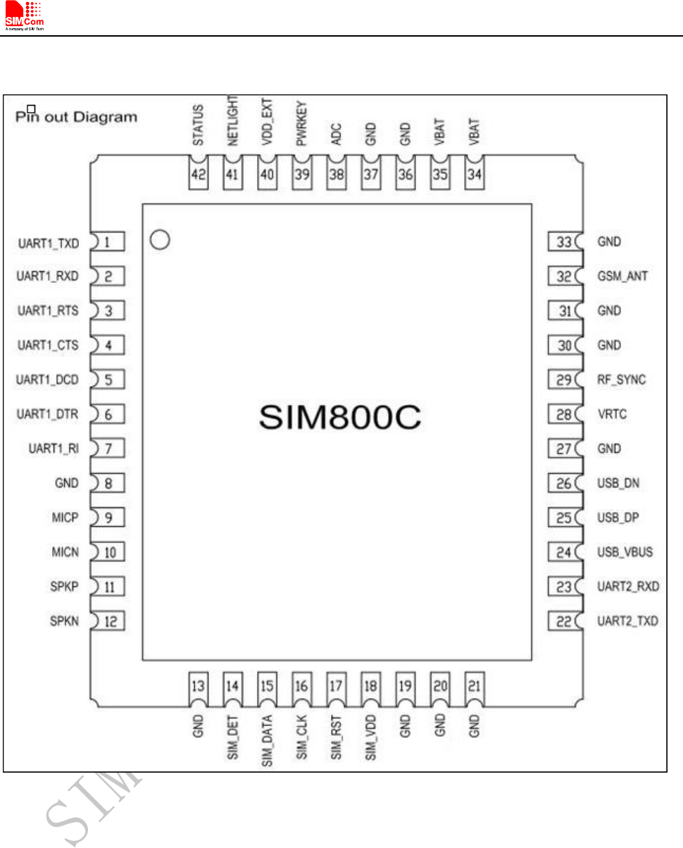
1.3. Pin
Smart Machine Smart Decision
- 5 -
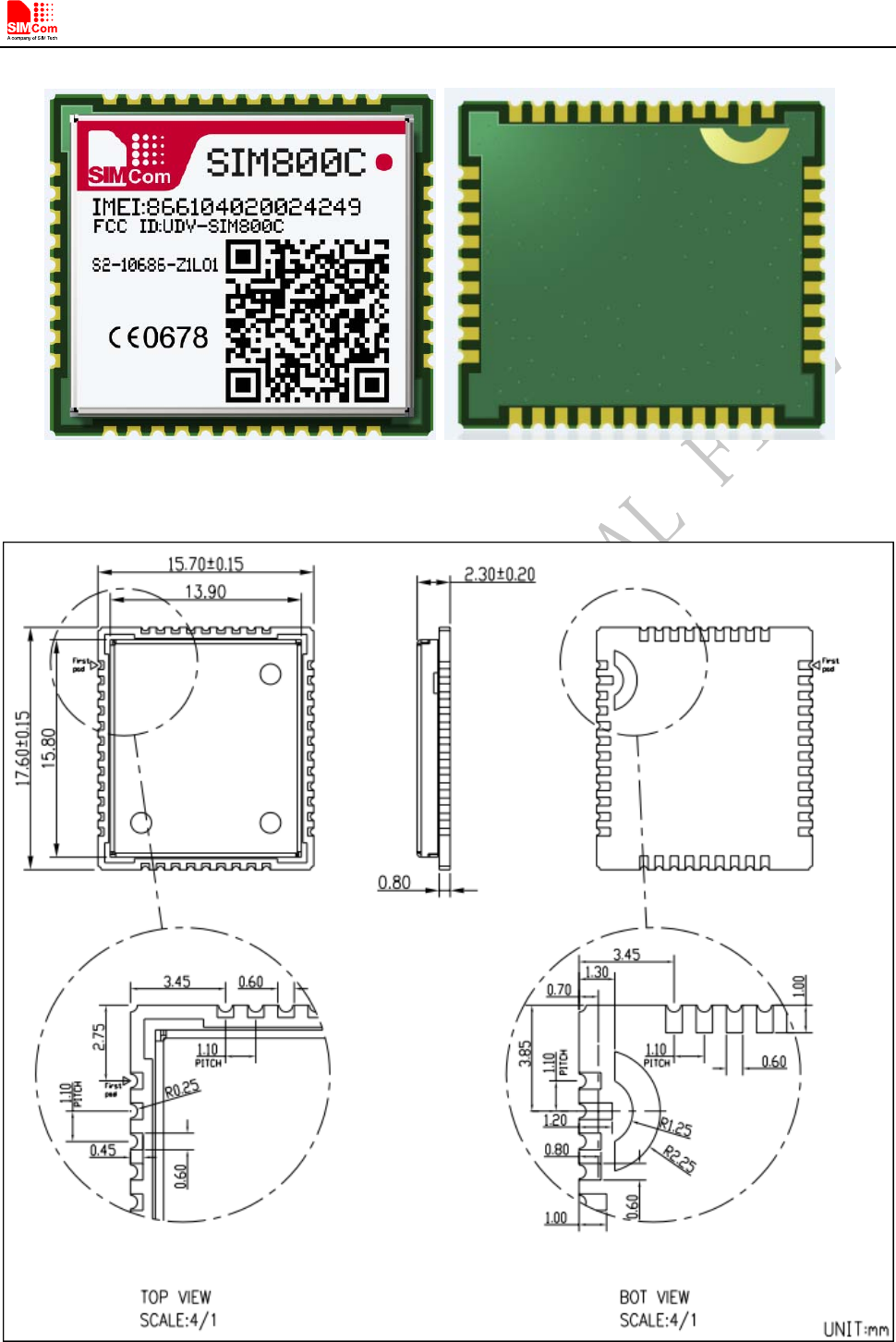
1.4. Picture
Figure 1: Top and Bottom view of SIM800C
1.5. Dimension
Figure 2: Dimention
Smart Machine Smart Decision
- 6 -
2. Detail Block Diagram
Figure 3: Block diagram of SIM800C
3. Electrical and Reliability Characteristics
3.1. Absolute Maximum Ratings
The absolute maximum ratings stated in following table are stress ratings under non-operating conditions. Stresses
beyond any of these limits will cause permanent damage to SIM800C.
Table 1: Absolute maximum ratings
Symbol Min Typ Max Unit
VBAT - - 4.5 V
Current 0 - 2.0 A
USB_VBUS - - 12 V
II* - 4 16 mA
IO* - 4 16 mA
*These parameters are for digital interface pins, GPIO, and UART.
3.2. Digital Interface Characteristics
Table 2: Digital interface characteristics
Smart Machine Smart Decision
- 7 -
Symbol Parameter Min Typ Max Unit
VIH High-level input current 2.1 - 3.1 V
VIL Low-level input current -0.3 - 0.7 V
VOH High-level output voltage 2.4 - - V
VOL Low-level output voltage - - 0.4 V
*Note: These parameters are for digital interface pins, such as keypad, GPIO and UART.
3.3. SIM Card Interface Characteristics
Table 3: SIM card interface characteristics
Symbol Parameter Min Typ Max Unit
IIH High-level input current -1.0 - 1.0 uA
IIL Low-level input current -1.0 - 1.0 uA
VIH High-level input voltage 1.4 - - V
2.4 - - V
VIL Low-level input voltage - - 0.27 V
0.4 V
VOH High-level output voltage 1.62 - - V
2.7 - - V
VOL Low-level output voltage - - 0.36 V
- - 0.4 V
3.4. SIM_VDD Characteristics
Table 4: SIM_VDD characteristics
Symbol Parameter Min Typ Max Unit
VO Output voltage - 3.0 - V
- 1.8 -
IO Output current - - 10 mA
3.5. VRTC Characteristics
Table 5: VRTC characteristics
Symbol Description Min Typ Max Unit
VRTC-IN VRTC input voltage 1.2 2.8 3.0 V
IRTC-IN VRTC input current - 3.0 5.0 uA
VRTC-OUT VRTC output voltage - 2.8 - V

Smart Machine Smart Decision
- 8 -
IRTC-OUT VRTC output current - 2.0 mA
3.6. Current Consumption (VBAT = 4.0V)
Table 6: Current consumption
Symbol Parameter Conditions Min Typ Max Unit
VBAT
Voltage 3.4 4.0 4.4 V
Power drop PCL=5 350 mV
Voltage ripple
PCL=5
@ f<200kHz
@ f>200kHz
50
2.0
mV
mV
IVBAT Average currnet
Power down mode 130 150 uA
Sleep mode (AT+CFUN=1):
( BS-PA-MFRMS=9 )
( BS-PA-MFRMS=5)
( BS-PA-MFRMS=2)
0.98
1.12
1.25
mA
mA
mA
Idle mode (AT+CFUN=1):
GSM850
EGSM900
DCS1800
PCS1900
13.8
13.8
13.8
13.8
mA
mA
mA
mA
Voice call (PCL=5):
GSM850
EGSM900
Voice call (PCL=0):
DCS1800
PCS1900
197
207
130
140
mA
mA
mA
mA
Data mode GPRS (1Rx,4Tx):
GSM850
EGSM900
DCS1800
PCS1900
394
416
271
285
mA
mA
mA
mA
Data mode GPRS (3Rx,2Tx):
GSM850
EGSM900
DCS1800
PCS1900
323
330
212
227
mA
mA
mA
mA
Data mode GPRS (4Rx,1Tx):
GSM850
EGSM900
DCS1800
PCS1900
213
210
150
162
mA
mA
mA
mA
Smart Machine Smart Decision
- 9 -
IMAX Peak current During Tx burst 2.0 A
3.7. Electro-Static Discharge
SIM800C is an ESD sensitive component, so more attention should be paid to the procedure of handling and
packaging. The ESD test results are shown in the following table.
Table 7: The ESD characteristics (Temperature: 25℃, Humidity: 45 %)
Pin name Contact discharge Air discharge
VBAT ±5KV ±12KV
GND ±6KV ±12KV
UARTX_RXD, UARTX_TXD ±2KV ±8KV
Antenna port ±6KV ±12KV
SPKP/SPKN/MICP/MICN ±3KV ±6KV
PWRKEY ±4KV ±8KV
4. Radio Characteristics
4.1. Module RF Output Power
The following table shows the module conducted output power, it is followed by the 3GPP TS 05.05 technical
specification requirement.
Table 8: SIM800C GSM 900 and GSM 850 conducted RF output power
GSM850,EGSM900
PCL Nominal output power (dBm) Tolerance (dB) for conditions
Normal Extreme
5 33 ±2 ±2.5
6 31 ±3 ±4
7 29 ±3 ±4
8 27 ±3 ±4
9 25 ±3 ±4
10 23 ±3 ±4
11 21 ±3 ±4
12 19 ±3 ±4
13 17 ±3 ±4
14 15 ±3 ±4
15 13 ±3 ±4
Smart Machine Smart Decision
- 10 -
16 11 ±5 ±6
17 9 ±5 ±6
18 7 ±5 ±6
19-31 5 ±5 ±6
Table 9: SIM800C DCS 1800 and PCS 1900 conducted RF output power
DCS1800,PCS1900
PCL Nominal output power (dBm) Tolerance (dB) for conditions
Normal Extreme
0 30 ±2 ±2.5
1 28 ±3 ±4
2 26 ±3 ±4
3 24 ±3 ±4
4 22 ±3 ±4
5 20 ±3 ±4
6 18 ±3 ±4
7 16 ±3 ±4
8 14 ±3 ±4
9 12 ±4 ±5
10 10 ±4 ±5
11 8 ±4 ±5
12 6 ±4 ±5
13 4 ±4 ±5
14 2 ±5 ±6
15 0 ±5 ±6
For the module’s output power, the following is should be noted:
At GSM900 and GSM850 band, the module is a class 4 device, so the module’s output power should not exceed
33dBm, and at the maximum power level, the output power tolerance should not exceed +/-2dB under normal
condition and +/-2.5dB under extreme condition.
At DCS1800 and PCS1900 band, the module is a class 1 device, so the module’s output power should not exceed
30dBm, and at the maximum power level, the output power tolerance should not exceed +/-2dB under normal
condition and +/-2.5dB under extreme condition.
4.2. Module RF Receive Sensitivity
The following table shows the module’s conducted receive sensitivity, it is tested under static condition.
Table 10: SIM800C conducted RF receive sensitivity
Smart Machine Smart Decision
- 11 -
Frequency Receive sensitivity(Typical) Receive sensitivity(Max)
GSM850,EGSM900 < -109dBm < -107dBm
DCS1800,PCS1900 < -109dBm < -107dBm
4.3. Module Operating Frequencies
The following table shows the module’s operating frequency range; it is followed by the 3GPP TS 05.05 technical
specification requirement.
Table 11: SIM800C operating frequencies
Frequency Receive Transmit
GSM850 869 ~ 894MHz 824 ~ 849MHz
EGSM900 925 ~ 960MHz 880 ~ 915MHz
DCS1800 1805 ~ 1880MHz 1710 ~ 1785MHz
PCS1900 1930 ~ 1990MHz 1850 ~ 1910MHz
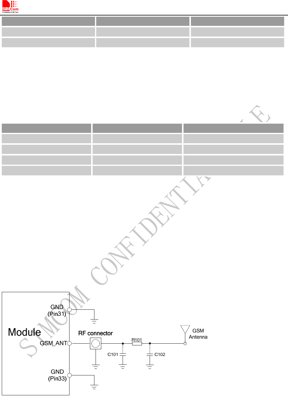
5. Antenna Interface
SIM800C provides GSM antenna named GSM_ANT, customer could use 50Ω microstrip line or stripline
antenna connect to the module.
The maximum gain of the Main antenna gain should not exceed 3dBi considering the SAR radio. No antenna
gain may be used that would exceed the 2W EIRP power limit in 1900MHz band.
It have according to reference trace and matching circuit testing all FCC items,and all items satisfy FCC
requirements.Only the reference trace and matching circuit is certified, antenna design must refer to it, any other
deviations require testing Class II applications as required by FCC.
The certified matching circuit as following:
Figure4: GSM antenna matching circuit
R101,C101,C102 are the matching circuit, the value should be defined by the antenna design. Normally R101
is 0Ω, C101 and C102 are not mounted.
Smart Machine Smart Decision
- 12 -
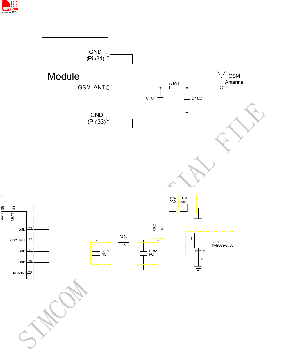
The RF connector is used for conduction test. If the space between RF pin and antenna is not enough, the
matching circuit should be designed as in the following figure:
Figure5: GSM antenna matching circuit without RF connector
Normally R101 is 0Ω, C101 and C102 are not mounted.
NC NC
0R
Smart Machine Smart Decision
- 13 -
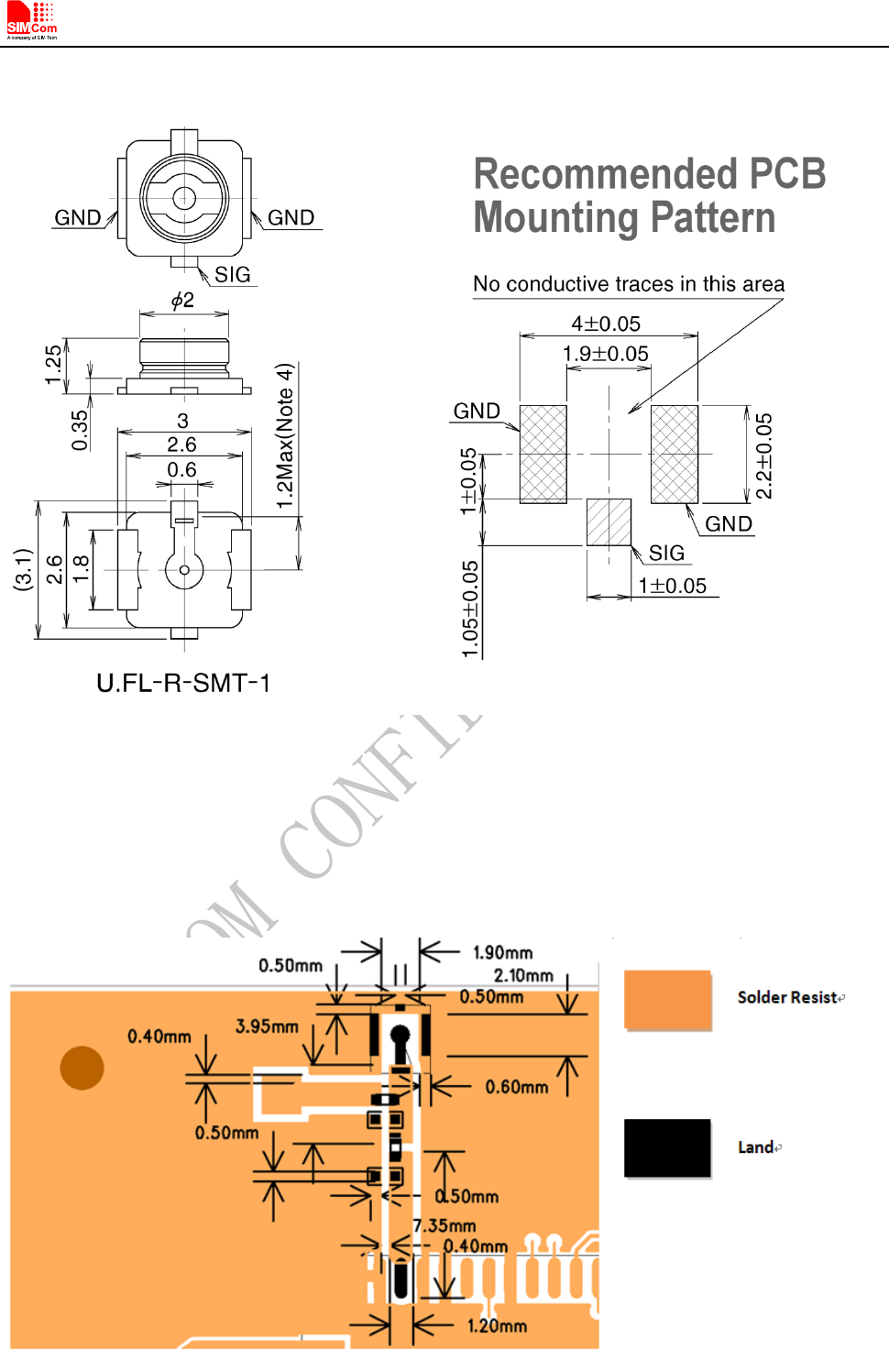
5.1. Dipole Antenna PCB Layout Requirements
5.2. Dipole Antenna Reference Design PCB
Mount these devices with brown mark facing up. Units: mm
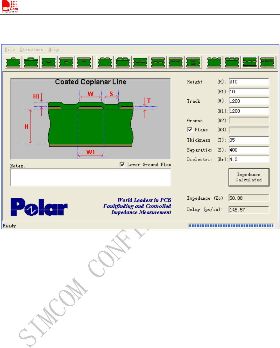
Line width should be designed to provide 50Ωimpedancematchingcharacteristics.
Smart Machine Smart Decision
- 14 -
LAYER1 - TOP
LAYER2 - BOTTOM
Smart Machine Smart Decision
- 15 -
MATERIAL BUILD-UP
Smart Machine Smart Decision
- 16 -
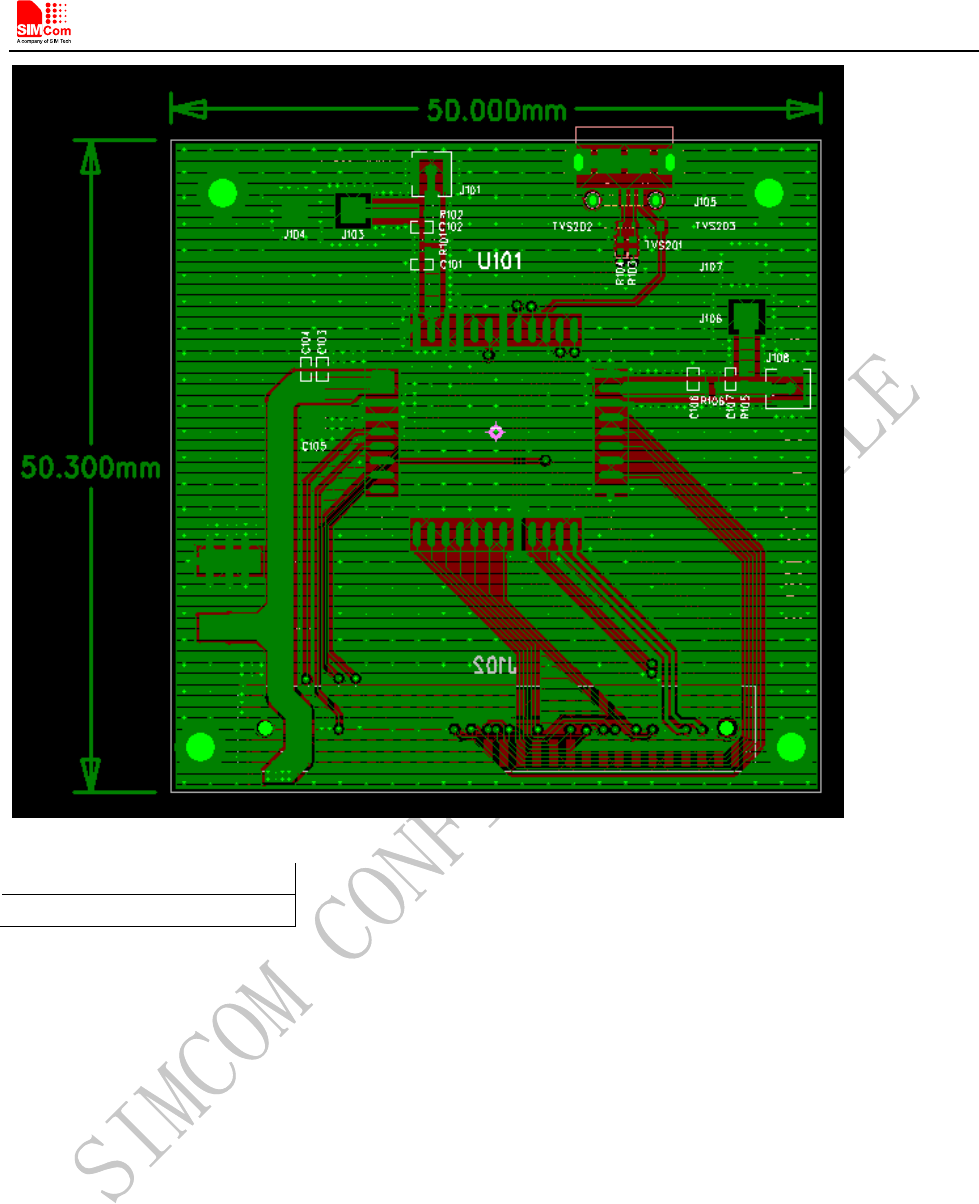
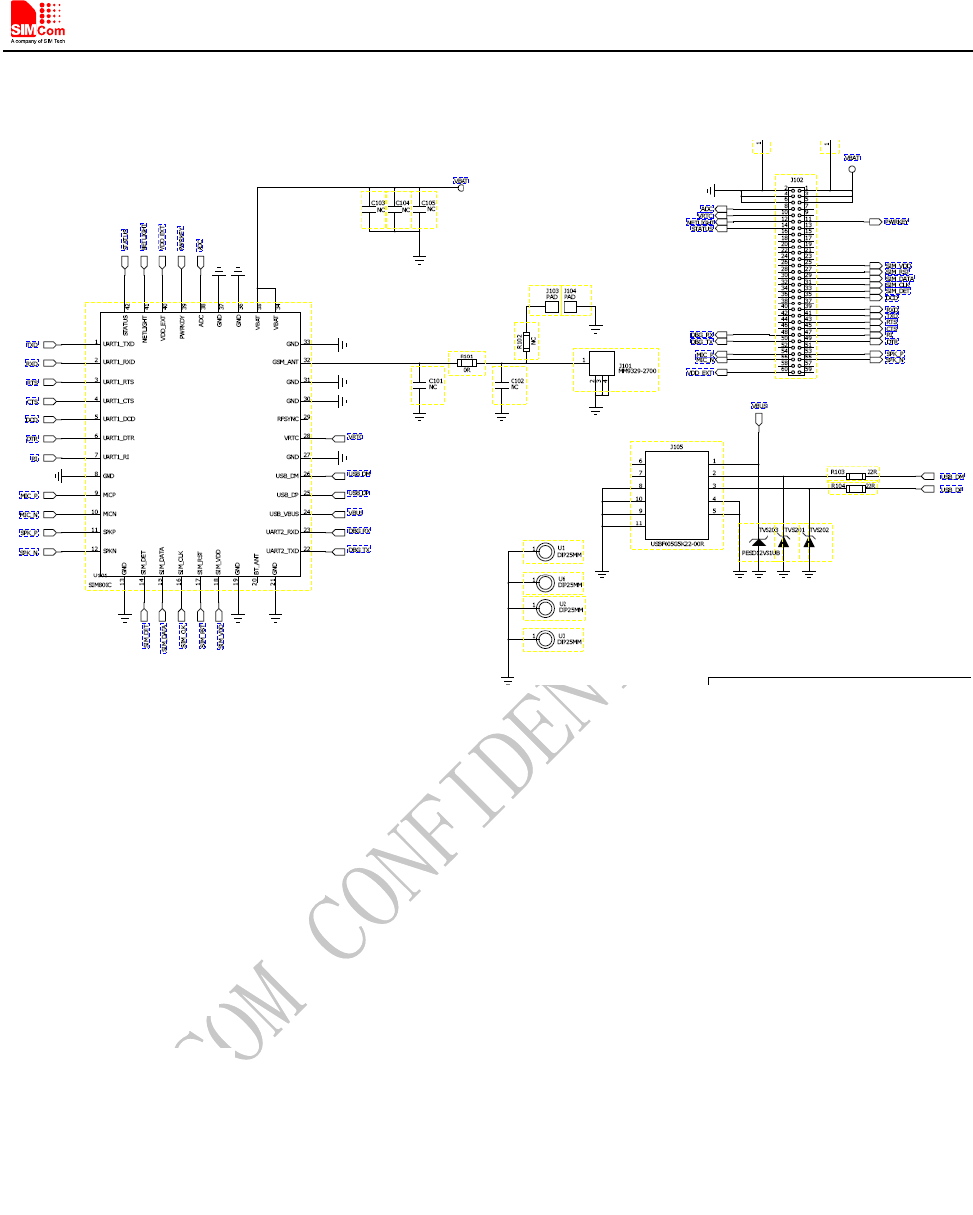
5.3. Dipole Antenna Reference Design Schematic
Smart Machine Smart Decision
- 17 -
Contact us:
Shanghai SIMCom Wireless Solutions Co.,Ltd.
Address: Building A, SIM Technology Building, No. 633, Jinzhong Road, Shanghai, P. R. China
200335
Tel: +86 21 3252 3300
Fax: +86 21 3252 2030
URL: www.sim.com/wm